US20020149392A1 - Level adjustment circuit and data output circuit thereof - Google Patents
Level adjustment circuit and data output circuit thereofDownload PDFInfo
- Publication number
- US20020149392A1 US20020149392A1US10/059,151US5915102AUS2002149392A1US 20020149392 A1US20020149392 A1US 20020149392A1US 5915102 AUS5915102 AUS 5915102AUS 2002149392 A1US2002149392 A1US 2002149392A1
- Authority
- US
- United States
- Prior art keywords
- node
- output
- level
- mos transistor
- inverter
- Prior art date
- Legal status (The legal status is an assumption and is not a legal conclusion. Google has not performed a legal analysis and makes no representation as to the accuracy of the status listed.)
- Granted
Links
Images


Classifications
- H—ELECTRICITY
- H03—ELECTRONIC CIRCUITRY
- H03K—PULSE TECHNIQUE
- H03K5/00—Manipulating of pulses not covered by one of the other main groups of this subclass
- H03K5/003—Changing the DC level
- H—ELECTRICITY
- H03—ELECTRONIC CIRCUITRY
- H03K—PULSE TECHNIQUE
- H03K3/00—Circuits for generating electric pulses; Monostable, bistable or multistable circuits
- H03K3/02—Generators characterised by the type of circuit or by the means used for producing pulses
- H03K3/353—Generators characterised by the type of circuit or by the means used for producing pulses by the use, as active elements, of field-effect transistors with internal or external positive feedback
- H03K3/356—Bistable circuits
- H03K3/356104—Bistable circuits using complementary field-effect transistors
- H03K3/356113—Bistable circuits using complementary field-effect transistors using additional transistors in the input circuit
- H—ELECTRICITY
- H03—ELECTRONIC CIRCUITRY
- H03K—PULSE TECHNIQUE
- H03K19/00—Logic circuits, i.e. having at least two inputs acting on one output; Inverting circuits
- H03K19/0008—Arrangements for reducing power consumption
- H03K19/0013—Arrangements for reducing power consumption in field effect transistor circuits
- H—ELECTRICITY
- H03—ELECTRONIC CIRCUITRY
- H03K—PULSE TECHNIQUE
- H03K19/00—Logic circuits, i.e. having at least two inputs acting on one output; Inverting circuits
- H03K19/0175—Coupling arrangements; Interface arrangements
- H03K19/0185—Coupling arrangements; Interface arrangements using field effect transistors only
- H03K19/018507—Interface arrangements
- H03K19/018521—Interface arrangements of complementary type, e.g. CMOS
Definitions
- the present inventionrelates to a semiconductor integrated circuit, and more particularly to a level adjustment circuit including a circuit operated by an inside power source voltage (VDD) and a data output circuit thereof.
- VDDinside power source voltage
- a level adjustment circuit for converting logic amplitude from an inside power source voltage (VDD) level to an outside power source voltage (VCC) levelincludes two NMOS transistors and two PMOS transistors connected to VCC and ground power source voltage. Each source electrode of the PMOS transistors is connected to VCC. Further, a gate electrode and a drain electrode are connected in a cross-coupling way with each other, and each of them is connected to the output node.
- An output level of this type of conventional level adjustment circuitis determined by the ON resistance ratio of the PMOS transistor and the NMOS transistor.
- the object of the present inventionis to provide a level adjustment circuit to shorten the time interval between the time at which a logic level of an output control signal of data changes and the time at which the logic level of an output of the level adjustment circuit changes.
- a level adjustment circuit of the present inventionincludes a MOS transistor for pulling up an output node, a first inverter for inputting output data signal and outputting a gate control signal for controlling a gate electrode of the MOS transistor, and a second inverter connected to the MOS transistor in series between first and second power sources for inputting a first node obtained based on the output data signal, and outputting the output node.
- the data output circuit of the present inventionincludes a first inverter connected to the first and second power sources for inputting output data signal and outputting to a first node, and a level adjustment circuit connected to the second power source and a third power source, electric potential of which is higher than the first power source, for outputting to a second node, in which the level adjustment circuit has a first MOS transistor for pulling up the second node, and a second inverter connected to the first MOS transistor in series between the second and third power sources; and a third inverter for inputting the data signal and outputting a gate control signal for controlling a gate electrode of the first MOS transistor.
- FIG. 1is a circuit diagram of the first and second preferred embodiments of the present invention.
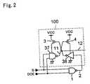
- FIG. 2is a circuit diagram of an equalizing circuit of a level adjustment circuit of the present invention
- FIG. 3is a circuit diagram of the third preferred embodiment of the present invention.
- FIG. 4is a circuit diagram of the fourth preferred embodiment of the present invention.
- FIG. 1is a diagram of a circuit of the first and second preferred embodiments of the present invention.
- a level adjustment circuit 100includes PMOS transistors 3 to 7 and NMOS transistors 8 to 10 .
- a source electrode, a gate electrode, and a drain electrode of a PMOS transistor 3are connected to VCC, an output node 12 , and a common source electrode of PMOS transistors 5 and 6 respectively.
- Drain electrodes of the PMOS transistors 5 and 6are connected to the output node 11 and each of gate electrodes thereof are connected to each of an output data signal D and an output control signal DOE respectively.
- a source electrode, a gate electrode, and a drain electrode of a PMOS transistor 4are connected to VCC, the output node 11 , and a source electrode of the PMOS transistor 7 respectively.
- a drain electrode of the PMOS transistor 7is connected to an output node 12 , and a gate electrode thereof is connected to an output 2 of NAND1, input electrodes of which are the output data signal D and the output control signal DOE.
- NAND1uses VDD and GND as power sources.
- a drain electrode, a gate electrode, and a source electrode of the NMOS transistor 8are connected to the output node 11 , the output control signal DOE, and a drain electrode of the NMOS transistor 9 respectively.
- a gate electrode of the NMOS transistor 9is connected to the output data signal D and a source electrode thereof is connected to GND.
- a drain electrode, a gate electrode, and a source electrode of the NMOS transistor 10are connected to the output node 12 , the output node 2 of NAND 1, and GND respectively.
- the PMOS transistors 5 to 7function as resistors.
- the resistance value thereofchanges to a maximum when the gate voltage of the PMOS transistors 5 to 7 is at the VDD level.
- the resistance value thereofchanges to a minimum when the gate voltage of the PMOS transistors 5 to 7 is at a ground level.
- a level adjustment circuit 101includes PMOS transistors 13 to 17 and NMOS transistors 18 to 20 .
- a source electrode, a gate electrode, and a drain electrode of PMOS transistors 13are connected to VCC, an output node 22 , and a common source bus of PMOS transistors 15 and 16 respectively.
- the drain electrodes of PMOS transistors 15 and 16are connected together with an output node 21 , and each of gate electrodes thereof is connected to either an output signal 72 of an inverter 71 to which an output data signal D is input or an output control signal ODE respectively.
- a source electrode, a gate electrode, and a drain electrode of a PMOS transistor 14are connected to VCC, the output node 21 , and a source electrode of the PMOS transistor 17 respectively.
- a drain electrode of the PMOS transistor 17is connected to the output node 22 , and a gate electrode thereof is connected to the output signal 72 of the inverter 71 and an output node 74 of NAND 73 to which the output signal 72 of the inverter 71 and the output control signal DOE are input.
- a drain electrode, a gate electrode, and a source electrode of the NMOS transistor 18are connected to the output node 21 , the output control signal DOE, and a drain electrode of the NMOS transistor 19 respectively.
- a gate electrode of the NMOS transistor 19is connected to the output signal 72 of the inverter 71 and a source electrode thereof is connected to GND.
- a drain electrode, a gate electrode, and a source electrode of the NMOS transistor 20are connected to the output node 22 , the output node 74 of the NAND 73, and GND respectively.
- the PMOS transistors 15 to 17function as the resistances in the same way as the PMOS transistors 5 to 7 . Similar to the conventional technology, NAND and the inverter use VDD and GND as the power sources. A logic amplitude of the output, the output signal D, and the output control signal DOE of NAND and the inverter, are at the VDD level.
- FIG. 2is an equivalent circuit to the level adjustment circuit of FIG. 1.
- the level adjustment circuit 100is explained as an example, and the same reference numbers in the two figures are used for the same components.
- the level adjustment circuit 100includes a NAND 37, to which the output data signal D and the output control signal DOE are input .
- the output node 11is output using VCC and GND as the power sources, and an inverter 38 for inputting the output node 2 and outputting the output node 12 .
- the PMOS transistor 3is a pull-up transistor for pulling-up the output node 12 , and the gate electrode is controlled by the output node 11 .
- NAND 1uses VDD and GND as power sources.
- the function of the level adjustment circuit of the preferred embodimentis explained using the level adjustment circuit 100 as an example.
- the output control signal DOEis at level L
- the NMOS transistor 10changes to an ON state.
- the output node 12is pulled down quickly and the PMOS transistor 3 changes to an ON state.
- the NMOS transistor 8changes to an OFF state. Since the resistance value by the PMOS transistor 6 changes to the minimum, the output node 11 is raised to the level H for about the same time as the conventional embodiment and the PMOS transistor 6 changes to the OFF state.
- the output control signal DOEchanges to the level H and the output data signal D changes from the level L to the level H.
- the output data signal Dchanges from the level L to the level H.
- the output node 2 of NAND 1changes from the level H to the level L.
- the resistance value of the PMOS transistorchanges from the maximum to the minimum, and the NMOS transistor 10 changes from the ON state to the OFF state.
- the resistance value of the PMOS transistors 5changes from the minimum to the maximum, and the NMOS transistor 9 changes from the OFF state to the ON state.
- the output node 11is quickly pulled down from the level H to the level L, and since the PMOS transistor 4 changes to the ON state, the output node 12 is rapidly pulled up from the level L to the level H.
- the output control signal DOEchanges to the level H and the output data signal D changes from the level H to the level L.
- the output data signal Dchanges from the level H to the level L
- the output node 2 of the NAND 1changes from the level L to the level H.
- the resistance value of the PMOS transistor 7changes from the minimum to the maximum
- the NMOS transistor 10changes from the OFF state to the ON state. Since the output data signal D maintains the level H, the PMOS transistor 4 remains in the ON state. Since the PMOS transistor 7 functions as the resistor, the output node 12 is pulled down rapidly from the level H to the level L, and the PMOS transistor 3 changes to the ON state.
- the resistance value of the PMOS transistor 5changes from the maximum to the minimum, and the NMOS transistor 9 changes from the ON state to the OFF state.
- the output node 11is rapidly raised to the level H from the level L, and the PMOS transistor 4 changes to the OFF state.
- the level adjustment circuit of the first preferred embodimentprovides the MOS transistor, in which the resistance value changes corresponding to an electric potential level applied to the gate electrode, for raising the output node.
- the gate electrodeis between the output node and the drain electrode of the MOS transistor. Compared with the conventional method, the time required to change the logic level of the output of the level adjustment circuit is reduced.
- the number of switching actions from the output data signal D to the output of the level adjustment circuitis lessened, the time required to output the changed logic level is reduced.
- the number of switching actions of the level adjustment circuit of the preferred embodimentis twice as few as the conventional circuits.
- the preferred embodimentrelates to the data output circuit including the level adjustment circuits 100 and 101 .
- An inverter 102uses VCC and GNO as power sources, and also includes a PMOS transistor 23 and NMOS transistors 24 and 25 . Gate electrodes of the PMOS transistor 23 and the NMOS transistor 24 are connected to the output node 12 of the level adjustment circuit 100 .
- a gate electrode of the NMOS transistor 25is connected to the output node 21 of the level adjustment circuit 101 , which has a reversed polarity to the output node 12 .
- the output node 29 of the inverter 102is connected to a gate electrode of the PMOS transistor 31 , which is the pull-up transistor for an output terminal DO.
- the inverter 103uses VCC and GND as power sources, and also includes PMOS transistors 26 and 27 and an NMOS transistor 28 . Gate electrodes of the PMOS transistor 27 and the NMOS transistor 28 are connected to the output node 21 of the level adjustment circuit 101 . A gate electrode of the PMOS transistor 26 is connected to an output node 12 of the level adjustment circuit 100 , which has a reversed polarity to the output node 21 . The output node 30 of the inverter 103 is connected to a gate electrode of an NMOS transistor 32 that is a pull-down transistor of the output terminal DO.
- the output node 29in the inverter 102 , is discharged through an ON resistance of the NMOS transistors 24 and 25 connected in series.
- the changing time of the logic level of the output node 29is delayed compared with a changing time of the logic level of the output node 30 of the inverter 103 . That is to say, the output terminal DO changes to the level H from the level L when the PMOS transistor 31 is in the ON state after the NMOS transistor 32 changes to the OFF state.
- the pull-up transistor (PMOS transistor 31 ) and the pull-down transistor (NMOS transistor 32 )change to the ON state at the same time, and excess current flowing from VCC to GND may be avoided
- FIG. 3is a circuit diagram showing the third preferred embodiment of the present invention.
- the third preferred embodimentis a modified embodiment in which the inverters 102 and 103 of the second preferred embodiment are modified.
- the inverter 104includes the PMOS transistor 33 and an NMOS transistor 34 connected in parallel between the drain electrodes of the output node 29 and the NMOS transistor 24 .
- Each gate electrode of the PMOS transistor 33 and the NMOS transistor 34is connected to each of GND and the output terminal DO singly, in the order designated.
- the inverter 105includes an NMOS transistor 35 and a PMOS transistor 36 connected in parallel between the drain electrode of the PMOS transistor 27 and the output node 30 .
- Each gate electrode of the NMOS transistor 35 and the PMOS transistor 36is connected to each of VCC and the output terminal DO.
- the output node 12changes to the level H from the level L when the output terminal DO and the output node 21 of the level adjustment circuit 101 are at the level L. Since the PMOS transistor 23 is in the ON state and the NMOS transistor 24 is in the OFF state when the output node 12 of the level adjustment circuit 100 is at the level L, the output node 29 and the PMOS transistor 31 of the inverter 104 are at the level H and OFF state respectively. When the output node 12 of the level adjustment circuit 100 changes to the level H, the PMOS transistor 23 changes to the OFF state and the NMOS transistor 24 changes to the ON state.
- the output node 29is pulled down through the PMOS transistor 33 and NMOS transistors 24 and 25 . Since the lower the electric potential level is, the higher the ON resistance value of the PMOS transistor 33 is, so the time required for change of the logic level is long. Electric discharge stops when the electric potential level approaches a threshold value of the PMOS transistor 33 . Since the PMOS transistor 31 changes to the ON state and the output terminal DO changes to the level H from the level L as the electric potential level of the output node 29 decreases, the NMOS transistor 34 changes to the ON state and the output node 29 is lowered to the level L.
- the output node 12changes to the level H from the level L when the output terminal DO and the output node 12 of the level adjustment circuit 100 are at the level L.
- the output node 12 of the level adjustment circuit 101is at the level H, since the PMOS transistor 27 is in the OFF state and the NMOS transistor 28 is in the ON state, the output node 30 of the inverter 105 is at the level L and the NMOS transistor 32 is in the OFF state.
- the output node 21 of the level adjustment circuit 101changes to the level L, the PMOS transistor 27 changes to the ON state and the NMOS transistor 28 changes to the OFF state.
- the output node 30is pulled up through the PMOS transistors 26 and 27 and the NMOS transistor 35 . Since the ON resistance value of the NMOS transistor 35 increases as the electric potential level increases, the time required for change of the logic level is long. Electric discharge stops when the electric potential level approaches a threshold value of the NMOS transistor 35 . Since the NMOS transistor 32 changes to the ON state and the output terminal DO is lowered to the level L from the level H as the electric potential level increases, the PMOS transistor 36 changes to the ON state and the output node 30 is pulled up to the level H.
- the rate of change of the current supplied by the PMOS transistor 31is rapid. Malfunction of the device and inducing power source noise based on an inductance component being parasitic on a lead frame of a package or a bonding wire connecting the output terminal DO, VCC, and the outside terminal, may be avoided. It naturally follows that the same result is obtained when the output terminal DO changes from the level H to the level L.
- FIG. 4is a circuit diagram showing the fourth preferred embodiment of the present invention.
- the fourth preferred embodimentis an embodiment in which elements of the inverters 106 and 107 of the third preferred embodiment are modified. In the following, modified portions are primarily explained.
- a source electrode of the PMOS transistor 33 of the inverter 106is connected to a substrate.
- a source electrode of the NMOS transistor 35 of the inverter 107is also connected to the substrate. Based on a substrate bias effect of both transistors of the PMOS transistor 33 and the NMOS transistor 35 , the increase in threshold value is suppressed.
- This type of componentis suitable in the case in which the data output circuit is operated using low power source voltage. To give an actual example, the power source voltage would be two to four times as high as the threshold value of the PMOS transistor 33 and the NMOS transistor 35 .
- the threshold value based on the substrate bias effect of the PMOS transistor 33 and the NMOS transistor 35does not increase, it is possible to increase the electric potential difference between the gate electrode and the source electrode of both transistors. As a result, the time required for changing the logic level of the output terminal DO may be shortened even if the data output circuit operates using the low power source voltage.
Landscapes
- Engineering & Computer Science (AREA)
- Computer Hardware Design (AREA)
- Physics & Mathematics (AREA)
- Computing Systems (AREA)
- General Engineering & Computer Science (AREA)
- Mathematical Physics (AREA)
- Nonlinear Science (AREA)
- Logic Circuits (AREA)
Abstract
Description
- 1. Field of the Invention[0001]
- The present invention relates to a semiconductor integrated circuit, and more particularly to a level adjustment circuit including a circuit operated by an inside power source voltage (VDD) and a data output circuit thereof.[0002]
- 2. Description of Related Art[0003]
- A level adjustment circuit for converting logic amplitude from an inside power source voltage (VDD) level to an outside power source voltage (VCC) level includes two NMOS transistors and two PMOS transistors connected to VCC and ground power source voltage. Each source electrode of the PMOS transistors is connected to VCC. Further, a gate electrode and a drain electrode are connected in a cross-coupling way with each other, and each of them is connected to the output node. An output level of this type of conventional level adjustment circuit is determined by the ON resistance ratio of the PMOS transistor and the NMOS transistor.[0004]
- However, according to the conventional circuit, there is a problem in which a time interval is long between time at which a logic level of data and the output control signal changes, and time at which a logic level of an output and level adjustment circuit changes, thus it is desired to improve the speed.[0005]
- The object of the present invention is to provide a level adjustment circuit to shorten the time interval between the time at which a logic level of an output control signal of data changes and the time at which the logic level of an output of the level adjustment circuit changes. A level adjustment circuit of the present invention includes a MOS transistor for pulling up an output node, a first inverter for inputting output data signal and outputting a gate control signal for controlling a gate electrode of the MOS transistor, and a second inverter connected to the MOS transistor in series between first and second power sources for inputting a first node obtained based on the output data signal, and outputting the output node. The data output circuit of the present invention includes a first inverter connected to the first and second power sources for inputting output data signal and outputting to a first node, and a level adjustment circuit connected to the second power source and a third power source, electric potential of which is higher than the first power source, for outputting to a second node, in which the level adjustment circuit has a first MOS transistor for pulling up the second node, and a second inverter connected to the first MOS transistor in series between the second and third power sources; and a third inverter for inputting the data signal and outputting a gate control signal for controlling a gate electrode of the first MOS transistor.[0006]
- While the specification concludes with claims claiming the subject matter regarded as the invention, the invention will be better understood based on the following description and the accompanying drawings related to this:[0007]
- FIG. 1 is a circuit diagram of the first and second preferred embodiments of the present invention;[0008]
- FIG. 2 is a circuit diagram of an equalizing circuit of a level adjustment circuit of the present invention;[0009]
- FIG. 3 is a circuit diagram of the third preferred embodiment of the present invention; and[0010]
- FIG. 4 is a circuit diagram of the fourth preferred embodiment of the present invention.[0011]
- The First Preferred Embodiment[0012]
- FIG. 1 is a diagram of a circuit of the first and second preferred embodiments of the present invention. A[0013]
level adjustment circuit 100 includesPMOS transistors 3 to7 andNMOS transistors 8 to10. A source electrode, a gate electrode, and a drain electrode of aPMOS transistor 3 are connected to VCC, anoutput node 12, and a common source electrode ofPMOS transistors PMOS transistors output node 11 and each of gate electrodes thereof are connected to each of an output data signal D and an output control signal DOE respectively. A source electrode, a gate electrode, and a drain electrode of aPMOS transistor 4 are connected to VCC, theoutput node 11, and a source electrode of the PMOS transistor7 respectively. A drain electrode of the PMOS transistor7 is connected to anoutput node 12, and a gate electrode thereof is connected to anoutput 2 of NAND1, input electrodes of which are the output data signal D and the output control signal DOE. NAND1 uses VDD and GND as power sources. - A drain electrode, a gate electrode, and a source electrode of the[0014]
NMOS transistor 8 are connected to theoutput node 11, the output control signal DOE, and a drain electrode of the NMOS transistor9 respectively. A gate electrode of the NMOS transistor9 is connected to the output data signal D and a source electrode thereof is connected to GND. A drain electrode, a gate electrode, and a source electrode of theNMOS transistor 10 are connected to theoutput node 12, theoutput node 2 ofNAND 1, and GND respectively. Here, when voltage difference between a VCC level and a VDD level is more than a threshold value, thePMOS transistors 5 to7 function as resistors. The resistance value thereof changes to a maximum when the gate voltage of thePMOS transistors 5 to7 is at the VDD level. On the contrary, the resistance value thereof changes to a minimum when the gate voltage of thePMOS transistors 5 to7 is at a ground level. - A[0015]
level adjustment circuit 101 includesPMOS transistors 13 to17 andNMOS transistors 18 to20. A source electrode, a gate electrode, and a drain electrode ofPMOS transistors 13 are connected to VCC, anoutput node 22, and a common source bus ofPMOS transistors PMOS transistors output node 21, and each of gate electrodes thereof is connected to either anoutput signal 72 of aninverter 71 to which an output data signal D is input or an output control signal ODE respectively. A source electrode, a gate electrode, and a drain electrode of aPMOS transistor 14 are connected to VCC, theoutput node 21, and a source electrode of thePMOS transistor 17 respectively. A drain electrode of thePMOS transistor 17 is connected to theoutput node 22, and a gate electrode thereof is connected to theoutput signal 72 of theinverter 71 and anoutput node 74 ofNAND 73 to which theoutput signal 72 of theinverter 71 and the output control signal DOE are input. - A drain electrode, a gate electrode, and a source electrode of the[0016]
NMOS transistor 18 are connected to theoutput node 21, the output control signal DOE, and a drain electrode of theNMOS transistor 19 respectively. A gate electrode of theNMOS transistor 19 is connected to theoutput signal 72 of theinverter 71 and a source electrode thereof is connected to GND. A drain electrode, a gate electrode, and a source electrode of theNMOS transistor 20 are connected to theoutput node 22, theoutput node 74 of theNAND 73, and GND respectively. Further, thePMOS transistors 15 to17 function as the resistances in the same way as thePMOS transistors 5 to7. Similar to the conventional technology, NAND and the inverter use VDD and GND as the power sources. A logic amplitude of the output, the output signal D, and the output control signal DOE of NAND and the inverter, are at the VDD level. - FIG. 2 is an equivalent circuit to the level adjustment circuit of FIG. 1. The[0017]
level adjustment circuit 100 is explained as an example, and the same reference numbers in the two figures are used for the same components. Thelevel adjustment circuit 100 includes aNAND 37, to which the output data signal D and the output control signal DOE are input . Theoutput node 11 is output using VCC and GND as the power sources, and aninverter 38 for inputting theoutput node 2 and outputting theoutput node 12. ThePMOS transistor 3 is a pull-up transistor for pulling-up theoutput node 12, and the gate electrode is controlled by theoutput node 11.NAND 1 uses VDD and GND as power sources. - The function of the level adjustment circuit of the preferred embodiment is explained using the[0018]
level adjustment circuit 100 as an example. When the output control signal DOE is at level L, since theoutput node 2 ofNAND 1 changes to level H unrelated to the output data signal D, theNMOS transistor 10 changes to an ON state. At this time, since the resistance value of the PMOS transistor changes to the maximum, theoutput node 12 is pulled down quickly and thePMOS transistor 3 changes to an ON state. On the other hand, theNMOS transistor 8 changes to an OFF state. Since the resistance value by thePMOS transistor 6 changes to the minimum, theoutput node 11 is raised to the level H for about the same time as the conventional embodiment and thePMOS transistor 6 changes to the OFF state. - It is explained, as an example, that the output control signal DOE changes to the level H and the output data signal D changes from the level L to the level H. When the output data signal D changes from the level L to the level H. the[0019]
output node 2 ofNAND 1 changes from the level H to the level L. Also at this time, the resistance value of the PMOS transistor changes from the maximum to the minimum, and theNMOS transistor 10 changes from the ON state to the OFF state. On the other hand, the resistance value of thePMOS transistors 5 changes from the minimum to the maximum, and the NMOS transistor9 changes from the OFF state to the ON state. As a result, theoutput node 11 is quickly pulled down from the level H to the level L, and since thePMOS transistor 4 changes to the ON state, theoutput node 12 is rapidly pulled up from the level L to the level H. - It is explained, as an example, that the output control signal DOE changes to the level H and the output data signal D changes from the level H to the level L. When the output data signal D changes from the level H to the level L, the[0020]
output node 2 of theNAND 1 changes from the level L to the level H. At this time, the resistance value of the PMOS transistor7 changes from the minimum to the maximum, and theNMOS transistor 10 changes from the OFF state to the ON state. Since the output data signal D maintains the level H, thePMOS transistor 4 remains in the ON state. Since the PMOS transistor7 functions as the resistor, theoutput node 12 is pulled down rapidly from the level H to the level L, and thePMOS transistor 3 changes to the ON state. On the other hand, the resistance value of thePMOS transistor 5 changes from the maximum to the minimum, and the NMOS transistor9 changes from the ON state to the OFF state. As a result, theoutput node 11 is rapidly raised to the level H from the level L, and thePMOS transistor 4 changes to the OFF state. An explanation of the functioning of thelevel adjustment circuit 101 is omitted, but it is easy to comprehend the functioning based on the operation of thelevel adjustment circuit 100. - As shown in the above, the level adjustment circuit of the first preferred embodiment provides the MOS transistor, in which the resistance value changes corresponding to an electric potential level applied to the gate electrode, for raising the output node. The gate electrode is between the output node and the drain electrode of the MOS transistor. Compared with the conventional method, the time required to change the logic level of the output of the level adjustment circuit is reduced.[0021]
- Further, since the number of switching actions from the output data signal D to the output of the level adjustment circuit is lessened, the time required to output the changed logic level is reduced. The number of switching actions of the level adjustment circuit of the preferred embodiment is twice as few as the conventional circuits.[0022]
- The Second Preferred Embodiment.[0023]
- The preferred embodiment relates to the data output circuit including the[0024]
level adjustment circuits inverter 102 uses VCC and GNO as power sources, and also includes aPMOS transistor 23 andNMOS transistors PMOS transistor 23 and theNMOS transistor 24 are connected to theoutput node 12 of thelevel adjustment circuit 100. A gate electrode of theNMOS transistor 25 is connected to theoutput node 21 of thelevel adjustment circuit 101, which has a reversed polarity to theoutput node 12. Theoutput node 29 of theinverter 102 is connected to a gate electrode of thePMOS transistor 31, which is the pull-up transistor for an output terminal DO. - The[0025]
inverter 103 uses VCC and GND as power sources, and also includesPMOS transistors NMOS transistor 28. Gate electrodes of thePMOS transistor 27 and theNMOS transistor 28 are connected to theoutput node 21 of thelevel adjustment circuit 101. A gate electrode of thePMOS transistor 26 is connected to anoutput node 12 of thelevel adjustment circuit 100, which has a reversed polarity to theoutput node 21. Theoutput node 30 of theinverter 103 is connected to a gate electrode of anNMOS transistor 32 that is a pull-down transistor of the output terminal DO. - The function of the data output circuit is explained using a case where the[0026]
output nodes inverters output node 12 of thelevel adjustment circuit 100 is the level L, thePMOS transistor 23 changes to the ON state and theNMOS transistor 24 changes to the OFF state. Therefore, anoutput node 29 changes to the level H and thePMOS transistor 31 changes to the OFF state whilst being completely unrelated to the ON or OFF state of theNMOS transistor 25. Further, when theoutput node 21 of theinverter 103 is at the level L, thePMOS transistors NMOS transistor 28 changes to the OFF state. Therefore, theoutput node 30 of theinverter 103 changes to the level H, and theNMOS transistor 32 changes to the ON state. At this time, the output terminal DO is at the level L. - When the[0027]
output node 21 of thelevel adjustment circuit 101 changes to the level H from the level L with a delay time t to the output node of thelevel adjustment circuit 100, thePMOS transistors NMOS transistor 24 changes to the ON state. Following this, thePMOS transistor 27 changes to the OFF state with the delay time t, and theNMOS transistors output nodes PMOS transistor 31 changes to the ON state from the OFF state and theNMOS transistor 32 changes to the OFF state from the ON state in that order. Theoutput node 29, in theinverter 102, is discharged through an ON resistance of theNMOS transistors output node 29 is delayed compared with a changing time of the logic level of theoutput node 30 of theinverter 103. That is to say, the output terminal DO changes to the level H from the level L when thePMOS transistor 31 is in the ON state after theNMOS transistor 32 changes to the OFF state. - Explanation of the function by which the[0028]
output nodes output node 30 in theinverter 103, is charged through the ON resistance of thePMOS transistors output node 30 is delayed compared with the logic level changing time of theoutput node 29 of theinverter 102. In other words, the output terminal DO changes to the level L from the level H when thePMOS transistor 31 changes to the ON state after thePMOS transistor 31 changes to the OFF state. - As shown above, according to the second preferred embodiment, the pull-up transistor (PMOS transistor[0029]31) and the pull-down transistor (NMOS transistor32) change to the ON state at the same time, and excess current flowing from VCC to GND may be avoided
- The Third Preferred Embodiment.[0030]
- FIG. 3 is a circuit diagram showing the third preferred embodiment of the present invention. The third preferred embodiment is a modified embodiment in which the[0031]
inverters inverter 104 includes thePMOS transistor 33 and anNMOS transistor 34 connected in parallel between the drain electrodes of theoutput node 29 and theNMOS transistor 24. Each gate electrode of thePMOS transistor 33 and theNMOS transistor 34 is connected to each of GND and the output terminal DO singly, in the order designated. Theinverter 105 includes anNMOS transistor 35 and aPMOS transistor 36 connected in parallel between the drain electrode of thePMOS transistor 27 and theoutput node 30. Each gate electrode of theNMOS transistor 35 and thePMOS transistor 36 is connected to each of VCC and the output terminal DO. - In order to explain how the data output circuit works, an example is explained where the[0032]
output node 12 changes to the level H from the level L when the output terminal DO and theoutput node 21 of thelevel adjustment circuit 101 are at the level L. Since thePMOS transistor 23 is in the ON state and theNMOS transistor 24 is in the OFF state when theoutput node 12 of thelevel adjustment circuit 100 is at the level L, theoutput node 29 and thePMOS transistor 31 of theinverter 104 are at the level H and OFF state respectively. When theoutput node 12 of thelevel adjustment circuit 100 changes to the level H, thePMOS transistor 23 changes to the OFF state and theNMOS transistor 24 changes to the ON state. Since thePMOS transistor 33 and theNMOS transistor 25 change to the ON state and theNMOS transistor 34 changes to the OFF state, theoutput node 29 is pulled down through thePMOS transistor 33 andNMOS transistors PMOS transistor 33 is, so the time required for change of the logic level is long. Electric discharge stops when the electric potential level approaches a threshold value of thePMOS transistor 33. Since thePMOS transistor 31 changes to the ON state and the output terminal DO changes to the level H from the level L as the electric potential level of theoutput node 29 decreases, theNMOS transistor 34 changes to the ON state and theoutput node 29 is lowered to the level L. - Furthermore, in this example, the[0033]
output node 12 changes to the level H from the level L when the output terminal DO and theoutput node 12 of thelevel adjustment circuit 100 are at the level L. When theoutput node 12 of thelevel adjustment circuit 101 is at the level H, since thePMOS transistor 27 is in the OFF state and theNMOS transistor 28 is in the ON state, theoutput node 30 of theinverter 105 is at the level L and theNMOS transistor 32 is in the OFF state. When theoutput node 21 of thelevel adjustment circuit 101 changes to the level L, thePMOS transistor 27 changes to the ON state and theNMOS transistor 28 changes to the OFF state. Since thePMOS transistor 26 and theNMOS transistor 35 are in the ON state and thePMOS transistor 36 is in the OFF state, theoutput node 30 is pulled up through thePMOS transistors NMOS transistor 35. Since the ON resistance value of theNMOS transistor 35 increases as the electric potential level increases, the time required for change of the logic level is long. Electric discharge stops when the electric potential level approaches a threshold value of theNMOS transistor 35. Since theNMOS transistor 32 changes to the ON state and the output terminal DO is lowered to the level L from the level H as the electric potential level increases, thePMOS transistor 36 changes to the ON state and theoutput node 30 is pulled up to the level H. - As shown in the above, according to the third embodiment, when the output terminal DO changes to the level H from the level L, since the time required for changing the logic level (at this time, changing from the level H to the level L) of the[0034]
output node 29 of theinverter 104 is long, the rate of change of the current supplied by thePMOS transistor 31 is rapid. Malfunction of the device and inducing power source noise based on an inductance component being parasitic on a lead frame of a package or a bonding wire connecting the output terminal DO, VCC, and the outside terminal, may be avoided. It naturally follows that the same result is obtained when the output terminal DO changes from the level H to the level L. - The Fourth Preferred Embodiment.[0035]
- FIG. 4 is a circuit diagram showing the fourth preferred embodiment of the present invention. The fourth preferred embodiment is an embodiment in which elements of the[0036]
inverters PMOS transistor 33 of theinverter 106 is connected to a substrate. A source electrode of theNMOS transistor 35 of theinverter 107 is also connected to the substrate. Based on a substrate bias effect of both transistors of thePMOS transistor 33 and theNMOS transistor 35, the increase in threshold value is suppressed. This type of component is suitable in the case in which the data output circuit is operated using low power source voltage. To give an actual example, the power source voltage would be two to four times as high as the threshold value of thePMOS transistor 33 and theNMOS transistor 35. - As shown in the above, according to the fourth embodiment, since the threshold value based on the substrate bias effect of the[0037]
PMOS transistor 33 and theNMOS transistor 35 does not increase, it is possible to increase the electric potential difference between the gate electrode and the source electrode of both transistors. As a result, the time required for changing the logic level of the output terminal DO may be shortened even if the data output circuit operates using the low power source voltage.
Claims (13)
1. A level adjustment circuit comprising:
a MOS transistor for pulling up an output node;
a first inverter for inputting an output data signal and outputting a gate control signal for controlling a gate electrode of said MOS transistor; and
a second inverter connected to said MOS transistor in series between first and second power sources, for inputting a first node obtained based on said output data signal, and outputting said output node.
2. A level adjustment circuit comprising:
a MOS transistor for pulling up an output node;
a logic gate for outputting a gate control signal for controlling a gate electrode of said MOS transistor by inputting an output data signal and a data output control signal; and
an inverter connected to said MOS transistor in series between first and second power sources for inputting a first node obtained based on said output data signal, and outputting said output node and said data output control signal.
3. A data output circuit comprising:
a first inverter connected to first and second power sources for inputting an output data signal and outputting a first node; and
a level adjustment circuit connected to said second power source and a third power source, electric potential of which is higher than said first power source, for outputting a second node,
wherein said level adjustment circuit has:
a first MOS transistor for pulling up said second node;
a second inverter connected to said first MOS transistor in series between the said second and third power sources; and
a third inverter for inputting said data signal and outputting a gate control signal for controlling a gate electrode of said first MOS transistor.
4. A data output circuit as claimed inclaim 3 further comprising an output driver including a fourth inverter for inputting said second node, and a second MOS transistor connected to said fourth inverter in series between said second and third power sources and controlled by a third node, a polarity of which is reverse of said second node.
5. A data output circuit as claimed inclaim 3 , further comprising:
third and fourth MOS transistors for inputting said second node;
a resistance connected to said third and fourth MOS transistors; and
a fifth MOS transistor connected to said third and fourth MOS transistors and said resistance in series and controlled by a third node, a polarity of which is reverse of said second node.
6. A data output circuit as claimed inclaim 5 , wherein said resistance is each of parallel sixth and seventh MOS transistors connected to said third and fourth MOS transistors.
7. A data output circuit as claimed inclaim 6 , wherein a source electrode of the said sixth MOS transistor is connected to a substrate.
8. A data output circuit comprising:
a first logic gate connected to first and second power sources for inputting an output data signal and a data output control signal and outputting a first node; and
a level adjustment circuit connected to said second power source and a third power source, electric potential of which is higher than said first power source, for outputting a second node, wherein said level adjustment circuit includes:
a first MOS transistor for pulling up said second node;
a first inverter connected to said first MOS transistor between said second and third power sources; and
a second logic gate for inputting said data signal and said data output control signal and outputting a gate control signal for controlling a gate electrode of said first MOS transistor.
9. A data output circuit as claimed inclaim 8 , further comprising an output driver including a second inverter for inputting said second node and a second MOS transistor connected to said second inverter in series between said second and third power sources and controlled by a third node, a polarity of which is reverse of said second node.
10. A data output circuit as claimed inclaim 8 , further comprising:
third and fourth MOS transistors for inputting said second node;
a resistance connected to said third and fourth MOS transistors; and
a fifth MOS transistor connected to said third and fourth MOS transistors and said resistance in series and controlled by said third node, a polarity of which is reverse of said second node.
11. A data output circuit as claimed inclaim 10 , wherein said resistance is each of parallel sixth and seventh MOS transistors connected to said third and fourth MOS transistors.
12. A data output circuit as claimed inclaim 11 , wherein a source electrode of said sixth MOS transistor is connected to a substrate.
13. A data output circuit comprising:
a first logic gate connected to first and second power sources for inputting an output data signal and a data output control signal and outputting a first node;
a second logic gate connected to said first and second power sources for inputting a reversed signal of said output data signal and said data output control signal and outputting a second node;
a first level adjustment circuit connected to said second power source and a third power source, electric potential of which is higher than said first power source, for outputting a third node corresponding to said first node; and
a second level adjustment circuit connected to said second power source and said third power source, electric potential of which is higher than said first power source, for outputting a fourth node corresponding to a reversed signal of said output data signal and said data output control signal,
wherein said first level adjustment circuit includes:
a first MOS transistor for pulling up said third node;
a first inverter connected to said first MOS transistor in series between said second and third power sources; and
a third logic gate for inputting said data signal and said data output control signal and outputting a first gate control signal for controlling a gate electrode of said MOS transistor; and said second level adjustment circuit includes:
a second MOS transistor for pulling up said fourth node;
a fourth logic gate connected to said MOS transistor in series between said second and third power sources; and
a second inverter for inputting said second node and outputting a second gate control signal for controlling said gate electrode of said MOS transistor.
Priority Applications (1)
| Application Number | Priority Date | Filing Date | Title |
|---|---|---|---|
| US10/059,151US6593795B2 (en) | 1999-11-18 | 2002-01-31 | Level adjustment circuit and data output circuit thereof |
Applications Claiming Priority (5)
| Application Number | Priority Date | Filing Date | Title |
|---|---|---|---|
| JP11-327834 | 1999-11-18 | ||
| JP32783499AJP2001144603A (en) | 1999-11-18 | 1999-11-18 | Level shifter circuit and data output circuit including it |
| JP327834/1999 | 1999-11-18 | ||
| US09/531,669US6459322B1 (en) | 1999-11-18 | 2000-03-20 | Level adjustment circuit and data output circuit thereof |
| US10/059,151US6593795B2 (en) | 1999-11-18 | 2002-01-31 | Level adjustment circuit and data output circuit thereof |
Related Parent Applications (1)
| Application Number | Title | Priority Date | Filing Date |
|---|---|---|---|
| US09/531,669ContinuationUS6459322B1 (en) | 1999-11-18 | 2000-03-20 | Level adjustment circuit and data output circuit thereof |
Publications (2)
| Publication Number | Publication Date |
|---|---|
| US20020149392A1true US20020149392A1 (en) | 2002-10-17 |
| US6593795B2 US6593795B2 (en) | 2003-07-15 |
Family
ID=18203513
Family Applications (2)
| Application Number | Title | Priority Date | Filing Date |
|---|---|---|---|
| US09/531,669Expired - Fee RelatedUS6459322B1 (en) | 1999-11-18 | 2000-03-20 | Level adjustment circuit and data output circuit thereof |
| US10/059,151Expired - Fee RelatedUS6593795B2 (en) | 1999-11-18 | 2002-01-31 | Level adjustment circuit and data output circuit thereof |
Family Applications Before (1)
| Application Number | Title | Priority Date | Filing Date |
|---|---|---|---|
| US09/531,669Expired - Fee RelatedUS6459322B1 (en) | 1999-11-18 | 2000-03-20 | Level adjustment circuit and data output circuit thereof |
Country Status (5)
| Country | Link |
|---|---|
| US (2) | US6459322B1 (en) |
| EP (1) | EP1102402A1 (en) |
| JP (1) | JP2001144603A (en) |
| KR (1) | KR20010049227A (en) |
| TW (1) | TW448620B (en) |
Cited By (21)
| Publication number | Priority date | Publication date | Assignee | Title |
|---|---|---|---|---|
| US20050007358A1 (en)* | 2003-05-20 | 2005-01-13 | Sung-Ho Lee | Driver circuit for driving display device, a display device having the same, and a method of driving the same |
| US20100187627A1 (en)* | 2008-03-13 | 2010-07-29 | Tela Innovations, Inc. | Channelized Gate Level Cross-Coupled Transistor Device with Overlapping PMOS Transistors and Overlapping NMOS Transistors Relative to Direction of Gate Electrodes |
| US20100277202A1 (en)* | 2006-03-09 | 2010-11-04 | Tela Innovations, Inc. | Circuitry and Layouts for XOR and XNOR Logic |
| US8471391B2 (en) | 2008-03-27 | 2013-06-25 | Tela Innovations, Inc. | Methods for multi-wire routing and apparatus implementing same |
| US8549455B2 (en) | 2007-08-02 | 2013-10-01 | Tela Innovations, Inc. | Methods for cell phasing and placement in dynamic array architecture and implementation of the same |
| US8658542B2 (en) | 2006-03-09 | 2014-02-25 | Tela Innovations, Inc. | Coarse grid design methods and structures |
| US8661392B2 (en) | 2009-10-13 | 2014-02-25 | Tela Innovations, Inc. | Methods for cell boundary encroachment and layouts implementing the Same |
| US8667443B2 (en) | 2007-03-05 | 2014-03-04 | Tela Innovations, Inc. | Integrated circuit cell library for multiple patterning |
| US8680626B2 (en) | 2007-10-26 | 2014-03-25 | Tela Innovations, Inc. | Methods, structures, and designs for self-aligning local interconnects used in integrated circuits |
| US8701071B2 (en) | 2008-01-31 | 2014-04-15 | Tela Innovations, Inc. | Enforcement of semiconductor structure regularity for localized transistors and interconnect |
| US8756551B2 (en) | 2007-08-02 | 2014-06-17 | Tela Innovations, Inc. | Methods for designing semiconductor device with dynamic array section |
| US8823062B2 (en) | 2006-03-09 | 2014-09-02 | Tela Innovations, Inc. | Integrated circuit with offset line end spacings in linear gate electrode level |
| US8839175B2 (en) | 2006-03-09 | 2014-09-16 | Tela Innovations, Inc. | Scalable meta-data objects |
| US8863063B2 (en) | 2009-05-06 | 2014-10-14 | Tela Innovations, Inc. | Finfet transistor circuit |
| US8951916B2 (en) | 2007-12-13 | 2015-02-10 | Tela Innovations, Inc. | Super-self-aligned contacts and method for making the same |
| US9035359B2 (en) | 2006-03-09 | 2015-05-19 | Tela Innovations, Inc. | Semiconductor chip including region including linear-shaped conductive structures forming gate electrodes and having electrical connection areas arranged relative to inner region between transistors of different types and associated methods |
| US9122832B2 (en) | 2008-08-01 | 2015-09-01 | Tela Innovations, Inc. | Methods for controlling microloading variation in semiconductor wafer layout and fabrication |
| US9159627B2 (en) | 2010-11-12 | 2015-10-13 | Tela Innovations, Inc. | Methods for linewidth modification and apparatus implementing the same |
| US9230910B2 (en) | 2006-03-09 | 2016-01-05 | Tela Innovations, Inc. | Oversized contacts and vias in layout defined by linearly constrained topology |
| US9563733B2 (en) | 2009-05-06 | 2017-02-07 | Tela Innovations, Inc. | Cell circuit and layout with linear finfet structures |
| US9754878B2 (en) | 2006-03-09 | 2017-09-05 | Tela Innovations, Inc. | Semiconductor chip including a chip level based on a layout that includes both regular and irregular wires |
Families Citing this family (10)
| Publication number | Priority date | Publication date | Assignee | Title |
|---|---|---|---|---|
| JP2001356741A (en)* | 2000-06-14 | 2001-12-26 | Sanyo Electric Co Ltd | Level shifter and active matrix type display device using the same |
| US6880032B1 (en)* | 2001-03-29 | 2005-04-12 | Emc Corporation | Data storage system having concurrent ESCON channels |
| JP3859483B2 (en)* | 2001-10-26 | 2006-12-20 | 沖電気工業株式会社 | Driving circuit |
| KR100518558B1 (en)* | 2003-02-18 | 2005-10-04 | 삼성전자주식회사 | Level shifter having low peak current |
| JP4576538B2 (en)* | 2004-05-12 | 2010-11-10 | 国立大学法人 岡山大学 | Integrated circuit with multidimensional switch topology |
| US7259610B1 (en)* | 2004-09-24 | 2007-08-21 | National Semiconductor Corporation | Static CMOS logic level shift circuit with a low logic input count high switching speed and low power dissipation |
| JP5158620B2 (en)* | 2007-02-20 | 2013-03-06 | セイコーエプソン株式会社 | Integrated circuit device and electronic apparatus |
| US20080297224A1 (en)* | 2007-06-01 | 2008-12-04 | Texas Instruments Incorporated | Minimizing Static Current Consumption While Providing Higher-Swing Output Signals when Components of an Integrated Circuit are Fabricated using a Lower-Voltage Process |
| US8638157B2 (en)* | 2011-05-23 | 2014-01-28 | Arm Limited | Level shifting circuitry |
| US12231121B2 (en)* | 2022-01-07 | 2025-02-18 | Mediatek Inc. | Multi-bit level shifter with shared enable signals |
Family Cites Families (21)
| Publication number | Priority date | Publication date | Assignee | Title |
|---|---|---|---|---|
| DE3855431T2 (en)* | 1987-10-14 | 1996-11-21 | Lsi Logic Corp | TWO FASHION DRIVER CIRCUIT |
| US4978870A (en)* | 1989-07-19 | 1990-12-18 | Industrial Technology Research Institute | CMOS digital level shifter circuit |
| JP2623918B2 (en)* | 1990-06-04 | 1997-06-25 | 日本電気株式会社 | Output buffer circuit |
| US5144165A (en)* | 1990-12-14 | 1992-09-01 | International Business Machines Corporation | CMOS off-chip driver circuits |
| JPH0567963A (en)* | 1991-09-06 | 1993-03-19 | Hitachi Ltd | Logic integrated circuit |
| JPH05102831A (en)* | 1991-10-09 | 1993-04-23 | Mitsubishi Electric Corp | Output circuit of semiconductor integrated circuit |
| JPH06164346A (en)* | 1992-11-25 | 1994-06-10 | Kawasaki Steel Corp | Output circuit |
| JPH06224732A (en)* | 1993-01-25 | 1994-08-12 | Nec Corp | Output buffer circuit provided with enable terminal |
| JP3311133B2 (en)* | 1994-02-16 | 2002-08-05 | 株式会社東芝 | Output circuit |
| JP3217224B2 (en)* | 1995-02-22 | 2001-10-09 | 富士通株式会社 | Level conversion circuit |
| US5644265A (en)* | 1995-05-01 | 1997-07-01 | International Business Machines Corporation | Off-chip driver for mixed voltage applications |
| JPH0983342A (en)* | 1995-09-19 | 1997-03-28 | Oki Micro Design Miyazaki:Kk | Semiconductor integrated circuit device |
| KR100189752B1 (en)* | 1996-06-01 | 1999-06-01 | 구본준 | Power pump circuit with independent well bias voltage |
| US5723987A (en)* | 1996-06-06 | 1998-03-03 | Intel Corporation | Level shifting output buffer with p channel pulldown transistors which are bypassed |
| EP0864203A4 (en)* | 1996-10-01 | 2001-02-07 | Microchip Tech Inc | High voltage level shifting cmos buffer |
| US5969554A (en)* | 1997-06-09 | 1999-10-19 | International Business Machines Corp. | Multi-function pre-driver circuit with slew rate control, tri-state operation, and level-shifting |
| JPH1155099A (en)* | 1997-07-29 | 1999-02-26 | Toshiba Microelectron Corp | Digital circuit |
| JP3796034B2 (en)* | 1997-12-26 | 2006-07-12 | 株式会社ルネサステクノロジ | Level conversion circuit and semiconductor integrated circuit device |
| JP3389856B2 (en)* | 1998-03-24 | 2003-03-24 | 日本電気株式会社 | Semiconductor device |
| JP2977556B1 (en)* | 1999-01-13 | 1999-11-15 | 沖電気工業株式会社 | Output circuit |
| US6262599B1 (en)* | 2000-04-06 | 2001-07-17 | International Business Machines Corporation | Level shifting CMOS I/O buffer |
- 1999
- 1999-11-18JPJP32783499Apatent/JP2001144603A/enactivePending
- 2000
- 2000-03-14TWTW089104566Apatent/TW448620B/ennot_activeIP Right Cessation
- 2000-03-14EPEP00105403Apatent/EP1102402A1/ennot_activeWithdrawn
- 2000-03-15KRKR1020000013132Apatent/KR20010049227A/ennot_activeCeased
- 2000-03-20USUS09/531,669patent/US6459322B1/ennot_activeExpired - Fee Related
- 2002
- 2002-01-31USUS10/059,151patent/US6593795B2/ennot_activeExpired - Fee Related
Cited By (109)
| Publication number | Priority date | Publication date | Assignee | Title |
|---|---|---|---|---|
| US20050007358A1 (en)* | 2003-05-20 | 2005-01-13 | Sung-Ho Lee | Driver circuit for driving display device, a display device having the same, and a method of driving the same |
| US7345683B2 (en)* | 2003-05-20 | 2008-03-18 | Samsung Electronics Co., Ltd. | Driver circuit for driving display device, a display device having the same, and a method of driving the same |
| US20080122818A1 (en)* | 2003-05-20 | 2008-05-29 | Samsung Electronics Co., Ltd. | Driver circuit for driving display device, a display device having the same, and a method of driving the same |
| US9336344B2 (en) | 2006-03-09 | 2016-05-10 | Tela Innovations, Inc. | Coarse grid design methods and structures |
| US9240413B2 (en) | 2006-03-09 | 2016-01-19 | Tela Innovations, Inc. | Methods, structures, and designs for self-aligning local interconnects used in integrated circuits |
| US10217763B2 (en) | 2006-03-09 | 2019-02-26 | Tela Innovations, Inc. | Semiconductor chip having region including gate electrode features of rectangular shape on gate horizontal grid and first-metal structures of rectangular shape on at least eight first-metal gridlines of first-metal vertical grid |
| US10186523B2 (en) | 2006-03-09 | 2019-01-22 | Tela Innovations, Inc. | Semiconductor chip having region including gate electrode features formed in part from rectangular layout shapes on gate horizontal grid and first-metal structures formed in part from rectangular layout shapes on at least eight first-metal gridlines of first-metal vertical grid |
| US10141334B2 (en) | 2006-03-09 | 2018-11-27 | Tela Innovations, Inc. | Semiconductor chip including region having rectangular-shaped gate structures and first-metal structures |
| US10141335B2 (en) | 2006-03-09 | 2018-11-27 | Tela Innovations, Inc. | Semiconductor CIP including region having rectangular-shaped gate structures and first metal structures |
| US8839175B2 (en) | 2006-03-09 | 2014-09-16 | Tela Innovations, Inc. | Scalable meta-data objects |
| US9917056B2 (en) | 2006-03-09 | 2018-03-13 | Tela Innovations, Inc. | Coarse grid design methods and structures |
| US9905576B2 (en) | 2006-03-09 | 2018-02-27 | Tela Innovations, Inc. | Semiconductor chip including region having rectangular-shaped gate structures and first metal structures |
| US9859277B2 (en) | 2006-03-09 | 2018-01-02 | Tela Innovations, Inc. | Methods, structures, and designs for self-aligning local interconnects used in integrated circuits |
| US10230377B2 (en) | 2006-03-09 | 2019-03-12 | Tela Innovations, Inc. | Circuitry and layouts for XOR and XNOR logic |
| US9741719B2 (en) | 2006-03-09 | 2017-08-22 | Tela Innovations, Inc. | Methods, structures, and designs for self-aligning local interconnects used in integrated circuits |
| US9711495B2 (en) | 2006-03-09 | 2017-07-18 | Tela Innovations, Inc. | Oversized contacts and vias in layout defined by linearly constrained topology |
| US9673825B2 (en) | 2006-03-09 | 2017-06-06 | Tela Innovations, Inc. | Circuitry and layouts for XOR and XNOR logic |
| US8653857B2 (en)* | 2006-03-09 | 2014-02-18 | Tela Innovations, Inc. | Circuitry and layouts for XOR and XNOR logic |
| US8658542B2 (en) | 2006-03-09 | 2014-02-25 | Tela Innovations, Inc. | Coarse grid design methods and structures |
| US20100277202A1 (en)* | 2006-03-09 | 2010-11-04 | Tela Innovations, Inc. | Circuitry and Layouts for XOR and XNOR Logic |
| US8921896B2 (en) | 2006-03-09 | 2014-12-30 | Tela Innovations, Inc. | Integrated circuit including linear gate electrode structures having different extension distances beyond contact |
| US9754878B2 (en) | 2006-03-09 | 2017-09-05 | Tela Innovations, Inc. | Semiconductor chip including a chip level based on a layout that includes both regular and irregular wires |
| US9589091B2 (en) | 2006-03-09 | 2017-03-07 | Tela Innovations, Inc. | Scalable meta-data objects |
| US9443947B2 (en) | 2006-03-09 | 2016-09-13 | Tela Innovations, Inc. | Semiconductor chip including region having integrated circuit transistor gate electrodes formed by various conductive structures of specified shape and position and method for manufacturing the same |
| US9425145B2 (en) | 2006-03-09 | 2016-08-23 | Tela Innovations, Inc. | Oversized contacts and vias in layout defined by linearly constrained topology |
| US9425272B2 (en) | 2006-03-09 | 2016-08-23 | Tela Innovations, Inc. | Semiconductor chip including integrated circuit including four transistors of first transistor type and four transistors of second transistor type with electrical connections between various transistors and methods for manufacturing the same |
| US9425273B2 (en) | 2006-03-09 | 2016-08-23 | Tela Innovations, Inc. | Semiconductor chip including integrated circuit including at least five gate level conductive structures having particular spatial and electrical relationship and method for manufacturing the same |
| US8823062B2 (en) | 2006-03-09 | 2014-09-02 | Tela Innovations, Inc. | Integrated circuit with offset line end spacings in linear gate electrode level |
| US8921897B2 (en) | 2006-03-09 | 2014-12-30 | Tela Innovations, Inc. | Integrated circuit with gate electrode conductive structures having offset ends |
| US9230910B2 (en) | 2006-03-09 | 2016-01-05 | Tela Innovations, Inc. | Oversized contacts and vias in layout defined by linearly constrained topology |
| US9035359B2 (en) | 2006-03-09 | 2015-05-19 | Tela Innovations, Inc. | Semiconductor chip including region including linear-shaped conductive structures forming gate electrodes and having electrical connection areas arranged relative to inner region between transistors of different types and associated methods |
| US9009641B2 (en) | 2006-03-09 | 2015-04-14 | Tela Innovations, Inc. | Circuits with linear finfet structures |
| US8952425B2 (en) | 2006-03-09 | 2015-02-10 | Tela Innovations, Inc. | Integrated circuit including at least four linear-shaped conductive structures having extending portions of different length |
| US8946781B2 (en) | 2006-03-09 | 2015-02-03 | Tela Innovations, Inc. | Integrated circuit including gate electrode conductive structures with different extension distances beyond contact |
| US9633987B2 (en) | 2007-03-05 | 2017-04-25 | Tela Innovations, Inc. | Integrated circuit cell library for multiple patterning |
| US8667443B2 (en) | 2007-03-05 | 2014-03-04 | Tela Innovations, Inc. | Integrated circuit cell library for multiple patterning |
| US10074640B2 (en) | 2007-03-05 | 2018-09-11 | Tela Innovations, Inc. | Integrated circuit cell library for multiple patterning |
| US9595515B2 (en) | 2007-03-07 | 2017-03-14 | Tela Innovations, Inc. | Semiconductor chip including integrated circuit defined within dynamic array section |
| US8966424B2 (en) | 2007-03-07 | 2015-02-24 | Tela Innovations, Inc. | Methods for cell phasing and placement in dynamic array architecture and implementation of the same |
| US9910950B2 (en) | 2007-03-07 | 2018-03-06 | Tela Innovations, Inc. | Methods for cell phasing and placement in dynamic array architecture and implementation of the same |
| US9424387B2 (en) | 2007-03-07 | 2016-08-23 | Tela Innovations, Inc. | Methods for cell phasing and placement in dynamic array architecture and implementation of the same |
| US8549455B2 (en) | 2007-08-02 | 2013-10-01 | Tela Innovations, Inc. | Methods for cell phasing and placement in dynamic array architecture and implementation of the same |
| US8759882B2 (en) | 2007-08-02 | 2014-06-24 | Tela Innovations, Inc. | Semiconductor device with dynamic array sections defined and placed according to manufacturing assurance halos |
| US8756551B2 (en) | 2007-08-02 | 2014-06-17 | Tela Innovations, Inc. | Methods for designing semiconductor device with dynamic array section |
| US10734383B2 (en) | 2007-10-26 | 2020-08-04 | Tela Innovations, Inc. | Methods, structures, and designs for self-aligning local interconnects used in integrated circuits |
| US8680626B2 (en) | 2007-10-26 | 2014-03-25 | Tela Innovations, Inc. | Methods, structures, and designs for self-aligning local interconnects used in integrated circuits |
| US10461081B2 (en) | 2007-12-13 | 2019-10-29 | Tel Innovations, Inc. | Super-self-aligned contacts and method for making the same |
| US9818747B2 (en) | 2007-12-13 | 2017-11-14 | Tela Innovations, Inc. | Super-self-aligned contacts and method for making the same |
| US8951916B2 (en) | 2007-12-13 | 2015-02-10 | Tela Innovations, Inc. | Super-self-aligned contacts and method for making the same |
| US9281371B2 (en) | 2007-12-13 | 2016-03-08 | Tela Innovations, Inc. | Super-self-aligned contacts and method for making the same |
| US9530734B2 (en) | 2008-01-31 | 2016-12-27 | Tela Innovations, Inc. | Enforcement of semiconductor structure regularity for localized transistors and interconnect |
| US9202779B2 (en) | 2008-01-31 | 2015-12-01 | Tela Innovations, Inc. | Enforcement of semiconductor structure regularity for localized transistors and interconnect |
| US8701071B2 (en) | 2008-01-31 | 2014-04-15 | Tela Innovations, Inc. | Enforcement of semiconductor structure regularity for localized transistors and interconnect |
| US8729606B2 (en) | 2008-03-13 | 2014-05-20 | Tela Innovations, Inc. | Integrated circuit including cross-coupled transistors having gate electrodes formed within gate level feature layout channels |
| US8669595B2 (en) | 2008-03-13 | 2014-03-11 | Tela Innovations, Inc. | Integrated circuit including cross-coupled transistors having gate electrodes formed within gate level feature layout channels with gate contact position, alignment, and offset specifications |
| US8772839B2 (en) | 2008-03-13 | 2014-07-08 | Tela Innovations, Inc. | Integrated circuit including cross-coupled transistors having gate electrodes formed within gate level feature layout channels with four inside positioned gate contacts having offset and aligned relationships and electrical connection of transistor gates through linear interconnect conductors in single interconnect layer |
| US8742463B2 (en) | 2008-03-13 | 2014-06-03 | Tela Innovations, Inc. | Integrated circuit including cross-coupled transistors having gate electrodes formed within gate level feature layout channels with outer positioned gate contacts |
| US8742462B2 (en) | 2008-03-13 | 2014-06-03 | Tela Innovations, Inc. | Integrated circuit including cross-coupled transistors having gate electrodes formed within gate level feature layout channels with gate contact position specifications |
| US9081931B2 (en) | 2008-03-13 | 2015-07-14 | Tela Innovations, Inc. | Cross-coupled transistor circuit having diffusion regions of common node on opposing sides of same gate electrode track and gate node connection through single interconnect layer |
| US9117050B2 (en) | 2008-03-13 | 2015-08-25 | Tela Innovations, Inc. | Integrated circuit including cross-coupled transistors having gate electrodes formed within gate level feature layout channels with gate contact position and offset specifications |
| US8785978B2 (en) | 2008-03-13 | 2014-07-22 | Tela Innovations, Inc. | Integrated circuit including cross-coupled transistors having gate electrodes formed within gate level feature layout channels with electrical connection of cross-coupled transistors through same interconnect layer |
| US10727252B2 (en) | 2008-03-13 | 2020-07-28 | Tela Innovations, Inc. | Semiconductor chip including integrated circuit having cross-coupled transistor configuration and method for manufacturing the same |
| US8872283B2 (en) | 2008-03-13 | 2014-10-28 | Tela Innovations, Inc. | Integrated circuit including cross-coupled transistors having gate electrodes formed within gate level feature layout channels with shared diffusion regions on opposite sides of two-transistor-forming gate level feature |
| US9208279B2 (en) | 2008-03-13 | 2015-12-08 | Tela Innovations, Inc. | Semiconductor chip including digital logic circuit including linear-shaped conductive structures having electrical connection areas located within inner region between transistors of different type and associated methods |
| US9213792B2 (en) | 2008-03-13 | 2015-12-15 | Tela Innovations, Inc. | Semiconductor chip including digital logic circuit including at least six transistors with some transistors forming cross-coupled transistor configuration and associated methods |
| US8735995B2 (en) | 2008-03-13 | 2014-05-27 | Tela Innovations, Inc. | Cross-coupled transistor circuit defined on three gate electrode tracks with diffusion regions of common node on opposing sides of same gate electrode track |
| US8735944B2 (en) | 2008-03-13 | 2014-05-27 | Tela Innovations, Inc. | Integrated circuit including cross-coupled transistors having gate electrodes formed within gate level feature layout channels with serially connected transistors |
| US9245081B2 (en) | 2008-03-13 | 2016-01-26 | Tela Innovations, Inc. | Semiconductor chip including digital logic circuit including at least nine linear-shaped conductive structures collectively forming gate electrodes of at least six transistors with some transistors forming cross-coupled transistor configuration and associated methods |
| US10658385B2 (en) | 2008-03-13 | 2020-05-19 | Tela Innovations, Inc. | Cross-coupled transistor circuit defined on four gate electrode tracks |
| US8866197B2 (en) | 2008-03-13 | 2014-10-21 | Tela Innovations, Inc. | Integrated circuit including cross-coupled transistors having gate electrodes formed within gate level feature layout channels with at least two gate electrodes electrically connected to each other through another transistor forming gate level feature |
| US8729643B2 (en) | 2008-03-13 | 2014-05-20 | Tela Innovations, Inc. | Cross-coupled transistor circuit including offset inner gate contacts |
| US10651200B2 (en) | 2008-03-13 | 2020-05-12 | Tela Innovations, Inc. | Cross-coupled transistor circuit defined on three gate electrode tracks |
| US8816402B2 (en) | 2008-03-13 | 2014-08-26 | Tela Innovations, Inc. | Integrated circuit including cross-coupled transistors having gate electrodes formed within gate level feature layout channels with gate level feature layout channel including single transistor |
| US8835989B2 (en) | 2008-03-13 | 2014-09-16 | Tela Innovations, Inc. | Integrated circuit including cross-coupled transistors having gate electrodes formed within gate level feature layout channels with gate electrode placement specifications |
| US8680583B2 (en) | 2008-03-13 | 2014-03-25 | Tela Innovations, Inc. | Integrated circuit including cross-coupled transistors having gate electrodes formed within at least nine gate level feature layout channels |
| US8853793B2 (en) | 2008-03-13 | 2014-10-07 | Tela Innovations, Inc. | Integrated circuit including gate electrode level region including cross-coupled transistors having gate contacts located over inner portion of gate electrode level region and offset gate level feature line ends |
| US8853794B2 (en) | 2008-03-13 | 2014-10-07 | Tela Innovations, Inc. | Integrated circuit within semiconductor chip including cross-coupled transistor configuration |
| US8847331B2 (en) | 2008-03-13 | 2014-09-30 | Tela Innovations, Inc. | Semiconductor chip including region having cross-coupled transistor configuration with offset electrical connection areas on gate electrode forming conductive structures and at least two different inner extension distances of gate electrode forming conductive structures |
| US20100187627A1 (en)* | 2008-03-13 | 2010-07-29 | Tela Innovations, Inc. | Channelized Gate Level Cross-Coupled Transistor Device with Overlapping PMOS Transistors and Overlapping NMOS Transistors Relative to Direction of Gate Electrodes |
| US9536899B2 (en) | 2008-03-13 | 2017-01-03 | Tela Innovations, Inc. | Semiconductor chip including integrated circuit having cross-coupled transistor configuration and method for manufacturing the same |
| US8785979B2 (en) | 2008-03-13 | 2014-07-22 | Tela Innovations, Inc. | Integrated circuit including cross-coupled transistors having gate electrodes formed within gate level feature layout channels with two inside positioned gate contacts and two outside positioned gate contacts and electrical connection of cross-coupled transistors through same interconnect layer |
| US8552509B2 (en) | 2008-03-13 | 2013-10-08 | Tela Innovations, Inc. | Integrated circuit including cross-coupled transistors having gate electrodes formed within gate level feature layout channels with other transistors positioned between cross-coupled transistors |
| US8669594B2 (en) | 2008-03-13 | 2014-03-11 | Tela Innovations, Inc. | Integrated circuit including cross-coupled transistors having gate electrodes formed within at least twelve gate level feature layout channels |
| US8552508B2 (en) | 2008-03-13 | 2013-10-08 | Tela Innovations, Inc. | Integrated circuit including cross-coupled transistors having gate electrodes formed within gate level feature layout channels with shared diffusion regions on opposite sides of two-transistor-forming gate level feature and electrical connection of transistor gates through linear interconnect conductors in single interconnect layer |
| US8592872B2 (en) | 2008-03-13 | 2013-11-26 | Tela Innovations, Inc. | Integrated circuit including cross-coupled transistors with two transistors of different type having gate electrodes formed by common gate level feature with shared diffusion regions on opposite sides of common gate level feature |
| US8558322B2 (en) | 2008-03-13 | 2013-10-15 | Tela Innovations, Inc. | Integrated circuit including cross-coupled transistors having gate electrodes formed within gate level feature layout channels with at least two gate electrodes electrically connected to each other through gate level feature |
| US8587034B2 (en) | 2008-03-13 | 2013-11-19 | Tela Innovations, Inc. | Integrated circuit including cross-coupled transistors having gate electrodes formed within gate level feature layout channels with four inside positioned gate contacts and electrical connection of transistor gates through linear interconnect conductors in single interconnect layer |
| US8581304B2 (en) | 2008-03-13 | 2013-11-12 | Tela Innovations, Inc. | Integrated circuit including cross-coupled transistors having gate electrodes formed within gate level feature layout channels with four inside positioned gate contacts having offset and aligned relationships |
| US8581303B2 (en) | 2008-03-13 | 2013-11-12 | Tela Innovations, Inc. | Integrated circuit including cross-coupled trasistors having gate electrodes formed within gate level feature layout channels with four inside positioned gate contacts having offset relationships and electrical connection of cross-coupled transistors through same interconnect layer |
| US10020321B2 (en) | 2008-03-13 | 2018-07-10 | Tela Innovations, Inc. | Cross-coupled transistor circuit defined on two gate electrode tracks |
| US8847329B2 (en) | 2008-03-13 | 2014-09-30 | Tela Innovations, Inc. | Cross-coupled transistor circuit defined having diffusion regions of common node on opposing sides of same gate electrode track with at least two non-inner positioned gate contacts |
| US8575706B2 (en) | 2008-03-13 | 2013-11-05 | Tela Innovations, Inc. | Integrated circuit including cross-coupled transistors having gate electrodes formed within gate level feature layout channels with at least two different gate level features inner extensions beyond gate electrode |
| US9871056B2 (en) | 2008-03-13 | 2018-01-16 | Tela Innovations, Inc. | Semiconductor chip including integrated circuit having cross-coupled transistor configuration and method for manufacturing the same |
| US8569841B2 (en) | 2008-03-13 | 2013-10-29 | Tela Innovations, Inc. | Integrated circuit including cross-coupled transistors having gate electrodes formed within gate level feature layout channels with at least one gate level feature extending into adjacent gate level feature layout channel |
| US8836045B2 (en) | 2008-03-13 | 2014-09-16 | Tela Innovations, Inc. | Cross-coupled transistor circuit having diffusion regions of common node on opposing sides of same gate electrode track |
| US8564071B2 (en) | 2008-03-13 | 2013-10-22 | Tela Innovations, Inc. | Integrated circuit including cross-coupled transistors having gate electrodes formed within gate level feature layout channels with at least two different gate level feature extensions beyond contact |
| US9390215B2 (en) | 2008-03-27 | 2016-07-12 | Tela Innovations, Inc. | Methods for multi-wire routing and apparatus implementing same |
| US8759985B2 (en) | 2008-03-27 | 2014-06-24 | Tela Innovations, Inc. | Methods for multi-wire routing and apparatus implementing same |
| US8471391B2 (en) | 2008-03-27 | 2013-06-25 | Tela Innovations, Inc. | Methods for multi-wire routing and apparatus implementing same |
| US9779200B2 (en) | 2008-03-27 | 2017-10-03 | Tela Innovations, Inc. | Methods for multi-wire routing and apparatus implementing same |
| US9122832B2 (en) | 2008-08-01 | 2015-09-01 | Tela Innovations, Inc. | Methods for controlling microloading variation in semiconductor wafer layout and fabrication |
| US9563733B2 (en) | 2009-05-06 | 2017-02-07 | Tela Innovations, Inc. | Cell circuit and layout with linear finfet structures |
| US10446536B2 (en) | 2009-05-06 | 2019-10-15 | Tela Innovations, Inc. | Cell circuit and layout with linear finfet structures |
| US8863063B2 (en) | 2009-05-06 | 2014-10-14 | Tela Innovations, Inc. | Finfet transistor circuit |
| US8661392B2 (en) | 2009-10-13 | 2014-02-25 | Tela Innovations, Inc. | Methods for cell boundary encroachment and layouts implementing the Same |
| US9530795B2 (en) | 2009-10-13 | 2016-12-27 | Tela Innovations, Inc. | Methods for cell boundary encroachment and semiconductor devices implementing the same |
| US9269702B2 (en) | 2009-10-13 | 2016-02-23 | Tela Innovations, Inc. | Methods for cell boundary encroachment and layouts implementing the same |
| US9704845B2 (en) | 2010-11-12 | 2017-07-11 | Tela Innovations, Inc. | Methods for linewidth modification and apparatus implementing the same |
| US9159627B2 (en) | 2010-11-12 | 2015-10-13 | Tela Innovations, Inc. | Methods for linewidth modification and apparatus implementing the same |
Also Published As
| Publication number | Publication date |
|---|---|
| EP1102402A1 (en) | 2001-05-23 |
| KR20010049227A (en) | 2001-06-15 |
| US6459322B1 (en) | 2002-10-01 |
| TW448620B (en) | 2001-08-01 |
| US6593795B2 (en) | 2003-07-15 |
| JP2001144603A (en) | 2001-05-25 |
Similar Documents
| Publication | Publication Date | Title |
|---|---|---|
| US6459322B1 (en) | Level adjustment circuit and data output circuit thereof | |
| US5568062A (en) | Low noise tri-state output buffer | |
| US5017807A (en) | Output buffer having capacitive drive shunt for reduced noise | |
| EP0493873B1 (en) | CMOS output buffer circuit with ground bounce reduction | |
| JP3038094B2 (en) | Output circuit of semiconductor integrated circuit device | |
| JPS63112893A (en) | Semiconductor integrated circuit | |
| US7656201B2 (en) | Output buffer circuit | |
| US20030001554A1 (en) | Internal power voltage generator | |
| US5801550A (en) | Output circuit device preventing overshoot and undershoot | |
| JPH05243940A (en) | Output buffer device | |
| JPH04229714A (en) | Integrated circuit having buffer | |
| US5059823A (en) | Supply bounce controlled output buffer circuit | |
| US20090289685A1 (en) | Bias voltage generation for capacitor-coupled level shifter with supply voltage tracking and compensation for input duty-cycle variation | |
| US6958626B2 (en) | Off chip driver | |
| US20030189452A1 (en) | Delay circuit and semiconductor device using the same | |
| JP2003017996A (en) | Level shift circuit | |
| US6833749B2 (en) | System and method for obtaining hysteresis through body substrate control | |
| EP1454414B1 (en) | High-speed output circuit with low voltage capability | |
| US7218145B2 (en) | Level conversion circuit | |
| JP2748865B2 (en) | Output circuit | |
| US6175598B1 (en) | Output noise control scheme for multiple I/O's | |
| US6472911B1 (en) | Output buffer circuit of semiconductor integrated circuit | |
| JP2006295322A (en) | Level shifter circuit | |
| US5319262A (en) | Low power TTL/CMOS receiver circuit | |
| JPH09214324A (en) | CMOS logic circuit |
Legal Events
| Date | Code | Title | Description |
|---|---|---|---|
| FEPP | Fee payment procedure | Free format text:PAYOR NUMBER ASSIGNED (ORIGINAL EVENT CODE: ASPN); ENTITY STATUS OF PATENT OWNER: LARGE ENTITY | |
| FPAY | Fee payment | Year of fee payment:4 | |
| AS | Assignment | Owner name:OKI SEMICONDUCTOR CO., LTD., JAPAN Free format text:CHANGE OF NAME;ASSIGNOR:OKI ELECTRIC INDUSTRY CO., LTD.;REEL/FRAME:022399/0969 Effective date:20081001 Owner name:OKI SEMICONDUCTOR CO., LTD.,JAPAN Free format text:CHANGE OF NAME;ASSIGNOR:OKI ELECTRIC INDUSTRY CO., LTD.;REEL/FRAME:022399/0969 Effective date:20081001 | |
| FPAY | Fee payment | Year of fee payment:8 | |
| AS | Assignment | Owner name:LAPIS SEMICONDUCTOR CO., LTD., JAPAN Free format text:CHANGE OF NAME;ASSIGNOR:OKI SEMICONDUCTOR CO., LTD;REEL/FRAME:032495/0483 Effective date:20111003 | |
| REMI | Maintenance fee reminder mailed | ||
| LAPS | Lapse for failure to pay maintenance fees | ||
| STCH | Information on status: patent discontinuation | Free format text:PATENT EXPIRED DUE TO NONPAYMENT OF MAINTENANCE FEES UNDER 37 CFR 1.362 | |
| FP | Lapsed due to failure to pay maintenance fee | Effective date:20150715 |