US20020148807A1 - Method of etching a deep trench in a substrate and method of fabricating on-chip devices and micro-machined structures using the same - Google Patents
Method of etching a deep trench in a substrate and method of fabricating on-chip devices and micro-machined structures using the sameDownload PDFInfo
- Publication number
- US20020148807A1 US20020148807A1US09/833,973US83397301AUS2002148807A1US 20020148807 A1US20020148807 A1US 20020148807A1US 83397301 AUS83397301 AUS 83397301AUS 2002148807 A1US2002148807 A1US 2002148807A1
- Authority
- US
- United States
- Prior art keywords
- etching
- substrate
- etch
- duration
- isotropic
- Prior art date
- Legal status (The legal status is an assumption and is not a legal conclusion. Google has not performed a legal analysis and makes no representation as to the accuracy of the status listed.)
- Granted
Links
- 238000005530etchingMethods0.000titleclaimsabstractdescription121
- 239000000758substrateSubstances0.000titleclaimsabstractdescription91
- 238000000034methodMethods0.000titleclaimsabstractdescription88
- 238000004519manufacturing processMethods0.000titleclaimsdescription13
- 230000000873masking effectEffects0.000claimsabstractdescription18
- 239000007789gasSubstances0.000claimsdescription29
- 239000003795chemical substances by applicationSubstances0.000claimsdescription26
- 239000002184metalSubstances0.000claimsdescription14
- 229910052751metalInorganic materials0.000claimsdescription14
- 229920002120photoresistant polymerPolymers0.000claimsdescription10
- 238000001020plasma etchingMethods0.000claimsdescription7
- 239000004642PolyimideSubstances0.000claimsdescription4
- 230000003287optical effectEffects0.000claimsdescription4
- 229920001721polyimidePolymers0.000claimsdescription4
- 239000003990capacitorSubstances0.000claimsdescription3
- XUIMIQQOPSSXEZ-UHFFFAOYSA-NSiliconChemical compound[Si]XUIMIQQOPSSXEZ-UHFFFAOYSA-N0.000abstractdescription25
- 229910052710siliconInorganic materials0.000abstractdescription25
- 239000010703siliconSubstances0.000abstractdescription25
- 230000008569processEffects0.000description11
- 239000000463materialSubstances0.000description10
- 238000002161passivationMethods0.000description5
- 238000012545processingMethods0.000description5
- 239000004065semiconductorSubstances0.000description4
- 230000008878couplingEffects0.000description3
- 238000010168coupling processMethods0.000description3
- 238000005859coupling reactionMethods0.000description3
- 238000002955isolationMethods0.000description3
- 230000003071parasitic effectEffects0.000description3
- KRHYYFGTRYWZRS-UHFFFAOYSA-NFluoraneChemical compoundFKRHYYFGTRYWZRS-UHFFFAOYSA-N0.000description2
- 238000013459approachMethods0.000description2
- 238000007747platingMethods0.000description2
- 229920000642polymerPolymers0.000description2
- RYGMFSIKBFXOCR-UHFFFAOYSA-NCopperChemical compound[Cu]RYGMFSIKBFXOCR-UHFFFAOYSA-N0.000description1
- 229910052581Si3N4Inorganic materials0.000description1
- VYPSYNLAJGMNEJ-UHFFFAOYSA-NSilicium dioxideChemical compoundO=[Si]=OVYPSYNLAJGMNEJ-UHFFFAOYSA-N0.000description1
- 230000000295complement effectEffects0.000description1
- 229910052802copperInorganic materials0.000description1
- 239000010949copperSubstances0.000description1
- 239000013078crystalSubstances0.000description1
- 238000000708deep reactive-ion etchingMethods0.000description1
- 238000011161developmentMethods0.000description1
- 238000010586diagramMethods0.000description1
- 229910044991metal oxideInorganic materials0.000description1
- 150000004706metal oxidesChemical class0.000description1
- 238000005459micromachiningMethods0.000description1
- 238000012986modificationMethods0.000description1
- 230000004048modificationEffects0.000description1
- 230000000149penetrating effectEffects0.000description1
- 229910021420polycrystalline siliconInorganic materials0.000description1
- 229920005591polysiliconPolymers0.000description1
- 238000011160researchMethods0.000description1
- HQVNEWCFYHHQES-UHFFFAOYSA-Nsilicon nitrideChemical compoundN12[Si]34N5[Si]62N3[Si]51N64HQVNEWCFYHHQES-UHFFFAOYSA-N0.000description1
- 229910052814silicon oxideInorganic materials0.000description1
- 239000000126substanceSubstances0.000description1
Images


Classifications
- B—PERFORMING OPERATIONS; TRANSPORTING
- B81—MICROSTRUCTURAL TECHNOLOGY
- B81C—PROCESSES OR APPARATUS SPECIALLY ADAPTED FOR THE MANUFACTURE OR TREATMENT OF MICROSTRUCTURAL DEVICES OR SYSTEMS
- B81C1/00—Manufacture or treatment of devices or systems in or on a substrate
- B81C1/00436—Shaping materials, i.e. techniques for structuring the substrate or the layers on the substrate
- B81C1/00555—Achieving a desired geometry, i.e. controlling etch rates, anisotropy or selectivity
- B81C1/00563—Avoid or control over-etching
- B81C1/00571—Avoid or control under-cutting
- H—ELECTRICITY
- H01—ELECTRIC ELEMENTS
- H01L—SEMICONDUCTOR DEVICES NOT COVERED BY CLASS H10
- H01L21/00—Processes or apparatus adapted for the manufacture or treatment of semiconductor or solid state devices or of parts thereof
- H01L21/02—Manufacture or treatment of semiconductor devices or of parts thereof
- H01L21/04—Manufacture or treatment of semiconductor devices or of parts thereof the devices having potential barriers, e.g. a PN junction, depletion layer or carrier concentration layer
- H01L21/18—Manufacture or treatment of semiconductor devices or of parts thereof the devices having potential barriers, e.g. a PN junction, depletion layer or carrier concentration layer the devices having semiconductor bodies comprising elements of Group IV of the Periodic Table or AIIIBV compounds with or without impurities, e.g. doping materials
- H01L21/30—Treatment of semiconductor bodies using processes or apparatus not provided for in groups H01L21/20 - H01L21/26
- H01L21/302—Treatment of semiconductor bodies using processes or apparatus not provided for in groups H01L21/20 - H01L21/26 to change their surface-physical characteristics or shape, e.g. etching, polishing, cutting
- H01L21/306—Chemical or electrical treatment, e.g. electrolytic etching
- H01L21/3065—Plasma etching; Reactive-ion etching
Definitions
- the present inventionrelates generally to etching trenches in substrates, and more specifically to a method of etching deep trenches in substrates that allows precise control of lateral undercut.
- the present inventionalso relates to a method of fabricating on-chip devices and micro-machined structures using the deep trench etching method.
- Trenchesare frequently etched in substrates to form micro-electromechanical devices, to form micro-machined structures such as cantilevers or optical mirrors, and to reduce electromagnetic coupling and parasitic capacitance between on-chip devices and the substrate.
- Such applications in which either an on-chip device or micro-machined structure is suspended over a trench etched in a substratepresent unique challenges for semiconductor manufacturers. This is because trench etching equipment has traditionally been used for either highly anisotropic etching or highly isotropic etching of substrates. In general, such highly anisotropic or isotropic etching cannot provide precise, controlled removal of substrate material located underneath on-chip devices and micro-machined structures.
- a micro-machined structuresuch as a cantilever
- a cantileveris formed by performing two (2) etching steps at opposing, non-normal angles to the substrate surface. The respective etching angles and depths are chosen such that the etched region completely undercuts and releases a portion of the substrate. Unetched substrate material under the released structure is then removed by exposing the reverse side of the substrate to a backside etch.
- the process steps described by Ho et al.are also complicated and can lead to higher manufacturing costs. Further, the process of Ho et al. can become increasingly difficult to use as die sizes are reduced and/or wafer sizes are increased. For example, as the thickness of a wafer increases, it generally becomes more difficult to perform a backside etch of the substrate.
- a method of etching a deep trench in a substratethat allows precise control of lateral undercut.
- the methodincludes the steps of optionally forming at least one on-chip device or micro-machined structure on a surface of a silicon substrate, and covering the surface with a masking layer such as photoresist, polyimide, metal, or oxide.
- a trench patternis then imaged in or transferred to the masking layer such that a trench subsequently etched in the substrate according to the pattern at least partially surrounds the optionally formed on-chip device or micro-machined structure.
- the device layeris etched using a standard passivation etch technique to expose at least a portion of the bulk silicon. Upper portions of the trench are then anisotropically etched in the silicon substrate using a dry plasma etch technique.
- C4F8 and SF6are employed as the active etching agents.
- the trenchis semi-anisotropically etched in the substrate with the C4F8 and SF6 active etching agents such that etching conditions are unchanged for the C4F8 anisotropic etching agent, but the etching conditions are modified for the SF6 isotropic etching agent.
- the etching conditions of the SF6 isotropic etching agentare modified to increase the pulse duration.
- the trenchis then isotropically etched in the substrate with the SF6 isotropic etching agent.
- the bias poweris reduced to a minimum during the isotropic etch.
- the remaining masking layeris stripped away.
- FIGS. 1 a - 1 bdepict sequential steps in fabricating an on-chip passive device such as an inductor
- FIGS. 2 a - 2 ddepict sequential steps in etching a trench in a substrate in accordance with the present invention.
- FIG. 3is a flow diagram depicting an exemplary method of etching a trench in a substrate in accordance with the present invention.
- a method of etching a laterally defined recess structure such as a trench or cavity in a substrateis disclosed.
- the presently disclosed etching methodallows precise control of lateral undercut, and can be employed to remove substrate material located underneath on-chip or micro-machined devices formed on the substrate.
- the disclosed etching methodis carried out using high density dry plasma etching equipment such as the ALCATEL 601 e etching system or any other suitable dry plasma etching equipment. Because the disclosed etching method employs a high density dry plasma etching technique, high etch consistency and high etch yield is achieved.
- the dry plasma etching techniqueis employed to etch a deep trench from the front side of the substrate, the need to perform a backside etch of the substrate is eliminated.
- the disclosed etching methodhas an etch rate of at least 7 ⁇ m/min, and can etch a deep trench in the silicon substrate down to a desired maximum depth with a precise, controlled lateral undercut.
- the chemicals employed with the disclosed methodinclude C4F8 and SF6.
- FIGS. 1 a - 1 bdepict sequential steps in fabricating an exemplary on-chip device.
- the presently disclosed deep trench etching methodmay be employed to etch a trench underneath the on-chip device, e.g., to reduce electromagnetic coupling and parasitic capacitance between the on-chip device and the substrate. It is understood that the disclosed etching method may be employed to etch trenches in substrates for other purposes, e.g., to provide isolation between adjacent on-chip devices, to contact a buried layer in the substrate, to form a micro-electromechanical device, and to release a micro-machined device such as a cantilever or an optical mirror.
- the disclosed methodis described herein in relation to the fabrication of exemplary on-chip devices for clarity of discussion.
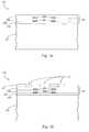
- FIG. 1 ashows a cross-sectional view of a portion 100 of a semiconductor wafer including a silicon substrate 102 and a device layer 104 .
- an on-chip devicesuch as an inductor, a capacitor, a transformer, a transistor, a micro-antenna or any other device that can be formed on a silicon substrate may be fabricated in the device layer 104 .
- CMOSComplementary Metal Oxide Semiconductor
- any suitable masking and plating techniquemay be used in fabricating the on-chip device.
- two (2) exemplary on-chip inductor devicesare fabricated in the device layer 104 using a standard double-poly double-metal CMOS process.
- the exemplary inductor devicescomprise respective first metal layer coil portions 106 a and respective second metal layer coil portions 106 b .
- the two (2) metal layers used to form the respective inductor coilsprovide low impedance and therefore reduce substrate losses.
- a first patterned dielectric layer 108 ais formed above the silicon substrate 102
- the first patterned metal layer 106 ais disposed on top of the first dielectric layer 108 a .
- a second patterned dielectric layer 108 bis formed above the first metal layer 106 a , and the second patterned metal layer 106 b is disposed on top of the second dielectric layer 108 b and over at least part of the first metal layer 106 a .
- the second dielectric layer 108 bincludes a plurality of vias (not shown) penetrating through the second dielectric layer 108 b to allow electrical connection between the respective first and second metal layer coil portions 106 a and 106 b of the two (2) inductors.
- a third patterned dielectric layer 108 cis then formed above the second metal layer 106 b.
- the surface of the device layer 104is coated with a masking layer 112 (see FIG. 1 b ) comprising, e.g., photoresist, polyimide, metal, and/or oxide.
- the masking layer 112comprises a photoresist layer that is from 6 to 10 ⁇ m thick and has an etching rate selectivity of photoresist to silicon equal to approximately 150:1.
- a trench patternis then imaged in the photoresist layer 112 such that a trench subsequently etched in the substrate according to the pattern at least partially surrounds the two (2) inductors.
- the trench patternmay define a plurality of openings 114 in the photoresist layer 112 . It is noted that any suitable number of openings 114 may be defined in the photoresist layer 112 to form the trench pattern.
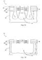
- FIGS. 2 a - 2 ddepict sequential steps in etching a deep trench in a substrate in accordance with the present invention.
- a deep trenchmay be etched underneath the two (2) on-chip inductor devices of FIGS. 1 a and 1 b to suspend the on-chip devices over the trench and reduce electromagnetic coupling and parasitic capacitance between the on-chip devices and the silicon substrate 102 .
- the device layer 104is etched using a standard passivation etch technique to form a plurality of cavities 216 (see FIG. 2 a ) that extend through the device layer 104 , thereby exposing at least a portion of the bulk silicon substrate 102 .
- the passivation etchis sufficient to allow the respective cavities 216 to extend completely through the device layer 104 and partially into the silicon substrate 102 . It is understood that the respective cavities 216 formed by the standard passivation etch technique comprise straight, vertical cavities with virtually no undercut.
- an anisotropic etchis performed on the exposed portions of the bulk silicon substrate 102 using a combination of the C4F8 and SF6 gases in a dry plasma etch technique.
- the anisotropic etchforms upper portions 220 a (see FIG. 2 b ) of a trench 220 (see FIGS. 2 c and 2 d ) in the silicon substrate 102 .
- the C4F8 and SF6 gasesare alternately pulsed.
- the C4F8 gaspreferably flows at a rate of 120 sccm with a pulse duration of 3 seconds, a source power of 2000 W, a bias power of 200 V, and a processing pressure of 3.5 Pa; and, the SF6 gas preferably flows at a rate of 240 sccm with a pulse duration of 10 seconds, a source power of 1600 W, a bias power of 200 V, and a processing pressure of 7.5 Pa.
- the anisotropic etchis a timed etch
- the depth of the anisotropic etchis proportional to the period of the anisotropic etch. In one embodiment, the anisotropic etch period is equal to 3 minutes. It is noted that the above-described anisotropic etch technique minimally undercuts the device layer 104 .
- a semi-anisotropic etchis then performed using the C4F8 anisotropic etching agent and the SF6 isotropic etching agent in the dry plasma etch technique.
- the semi-anisotropic etchforms the trench 220 (see FIG. 2 c ) in the silicon substrate 102 .
- the C4F8 and SF6 gasesare alternately pulsed.
- the C4F8 gaspreferably flows at a rate of 120 sccm with a pulse duration of 3 seconds, a source power of 2000 W, a bias power of 200 V, and a processing pressure of 3.5 Pa; and, the SF6 gas preferably flows at a rate of 240 sccm with a pulse duration of 30 seconds, a source power of 1600 W, a bias power of 150 V, and a processing pressure of 7.5 Pa. Because the pulse duration is increased and the bias level is reduced for the SF6 isotropic etching agent, the affect of the SF6 isotropic etching agent is enhanced compared to the initial anisotropic etch.
- the C4F8 gasis primarily employed for anisotropically etching the trench 220 vertically in the silicon substrate 102
- the SF6 gasis primarily employed for isotropically etching the trench 220 vertically and laterally in the silicon substrate 102 .
- the shape of the trench 220can be precisely controlled, e.g., by adjusting the flow rate, pulse duration, and/or the bias power for the SF6 isotropic etching agent. Because the semi-anisotropic etch is a timed etch, a predetermined depth 222 (see FIG.
- the semi-anisotropic etch periodis sufficient to allow the predetermined depth 222 of the trench 220 to be approximately equal to 300 ⁇ m, and the lateral undercut to be approximately zero. In one embodiment, the semi-anisotropic etch period is equal to 15 minutes. It is noted that the semi-anisotropic etch forms re-entrant shapes in respective sidewalls 224 (see FIG. 2 c ) of the trench 220 . Further, at least one wall 226 (see FIG. 2 c ) of substrate material may remain directly underneath the on-chip devices at the completion of the semi-anisotropic etch.
- an isotropic etchis performed using the SF6 gas and the dry plasma etch technique.
- the SF6 gasflows at a rate of 500 sccm with a source power of 2000 W, a bias power of 60 V, and a processing pressure of 22 Pa.
- the preferred isotropic etch conditionsare sufficient to remove the walls 226 (see FIG. 2 c ) of substrate material directly below the two (2) on-chip inductor devices.
- the trench 220extends laterally in the silicon substrate 102 with very small spikes of substrate material underneath the respective devices. It is noted that the isotropic etch is a timed etch.
- the isotropic etch periodis sufficient to allow the complete removal of the walls 226 of substrate material from the trench 220 , and to allow a predetermined depth 228 of the trench 220 to be approximately equal to 400 ⁇ m. In one embodiment, the isotropic etch period is equal to 15 minutes. It is further noted that the isotropic etch causes a relatively small amount of undercut in the respective sidewalls 224 of the trench 220 . Finally, the remaining photoresist layer 112 is stripped from the surface of the device layer 104 using any suitable technique.
- step 30at least one on-chip device is optionally formed in a device layer of a silicon substrate using any suitable silicon process.
- the surface of the device layeris coated, as depicted in step 32 , with a suitable masking layer, and a trench pattern is imaged in or transferred to the masking layer.
- the device layeris then etched, as depicted in step 34 , using a standard passivation etch technique to expose at least a portion of the bulk silicon substrate.
- an anisotropic etchis performed, as depicted in step 36 , to form upper portions of a trench having a first predetermined depth in the substrate; and, a semi-anisotropic etch is performed, as depicted in step 37 , to form the trench to a second predetermined depth with approximately zero lateral undercut. It is noted that a re-entrant shape is formed in the trench.
- An isotropic etchis then performed, as depicted in step 38 , to remove any walls of substrate material that may remain directly underneath the on-chip device and achieve a final predetermined depth of the trench.
- any remaining masking layeris stripped, as depicted in step 39 , from the surface of the device layer.
- the isotropic etchcauses a relatively small amount of undercut to occur in the regions of the trench sidewalls 224 (see FIG. 2 c ).
- Such undercutmay be further controlled by covering the sidewalls 224 and bottom surface (not numbered) of the trench 220 with a suitable polymer at least once before or during the performance of the anisotropic etch and/or the semi-anisotropic etch.
- a suitable polymerat least once before or during the performance of the anisotropic etch and/or the semi-anisotropic etch.
- etching agentsmay be used in carrying out the presently disclosed etching method instead of the C4F8 and SF6 gases. It is understood, however, that in order to derive the benefits of the disclosed method, the alternative etching agents should be used in conjunction with suitable etching conditions to produce at least an anisotropic etch followed by a semi-anisotropic etch to achieve deep trench etching with precise control of lateral undercut.
Landscapes
- Engineering & Computer Science (AREA)
- Physics & Mathematics (AREA)
- Microelectronics & Electronic Packaging (AREA)
- Manufacturing & Machinery (AREA)
- Condensed Matter Physics & Semiconductors (AREA)
- Plasma & Fusion (AREA)
- Geometry (AREA)
- General Physics & Mathematics (AREA)
- Computer Hardware Design (AREA)
- Power Engineering (AREA)
- Drying Of Semiconductors (AREA)
- Micromachines (AREA)
- Element Separation (AREA)
Abstract
Description
- N/A[0001]
- N/A[0002]
- The present invention relates generally to etching trenches in substrates, and more specifically to a method of etching deep trenches in substrates that allows precise control of lateral undercut. The present invention also relates to a method of fabricating on-chip devices and micro-machined structures using the deep trench etching method.[0003]
- Trenches are frequently etched in substrates to form micro-electromechanical devices, to form micro-machined structures such as cantilevers or optical mirrors, and to reduce electromagnetic coupling and parasitic capacitance between on-chip devices and the substrate. Such applications in which either an on-chip device or micro-machined structure is suspended over a trench etched in a substrate present unique challenges for semiconductor manufacturers. This is because trench etching equipment has traditionally been used for either highly anisotropic etching or highly isotropic etching of substrates. In general, such highly anisotropic or isotropic etching cannot provide precise, controlled removal of substrate material located underneath on-chip devices and micro-machined structures.[0004]
- One approach to fabricating on-chip devices is described in a publication entitled[0005]A Universal MEMS Fabrication Process for High-Performance On-Chip RF Passive Components and Circuits, Jiang et al., Solid-State Sensor and Actuator Workshop, June 2000. According to that fabrication process, silicon nitride is deposited and patterned on the substrate surface as an isolation layer, a trench is etched in the substrate by deep reactive ion etching, and a sacrificial silicon-oxide block is formed in the trench and on the isolation layer. Next, an on-chip device suspended over the trench is built by polysilicon surface micro-machining and released in hydrofluoric acid, and copper plating is performed. However, one drawback of the process of Jiang et al. is that it includes many complicated steps that can significantly increase costs of manufacture.
- One approach to fabricating a micro-machined structure such as a cantilever is described in U.S. Pat. No. 6,086,774 issued to Ho et al. According to that fabrication process, a cantilever is formed by performing two (2) etching steps at opposing, non-normal angles to the substrate surface. The respective etching angles and depths are chosen such that the etched region completely undercuts and releases a portion of the substrate. Unetched substrate material under the released structure is then removed by exposing the reverse side of the substrate to a backside etch. However, the process steps described by Ho et al. are also complicated and can lead to higher manufacturing costs. Further, the process of Ho et al. can become increasingly difficult to use as die sizes are reduced and/or wafer sizes are increased. For example, as the thickness of a wafer increases, it generally becomes more difficult to perform a backside etch of the substrate.[0006]
- Still another fabrication process is described in U.S. Pat. No. 4,600,934 issued to Aine et al. According to that fabrication process, an etch resistant layer is deposited on the substrate surface, angled notches are formed in the etch resistant layer, and anisotropic undercut etching is performed in the region of the notches. The rate of undercut etching is determined by the angle of the notches relative to the crystal planes of the substrate. However, the process steps described by Aine et al. are also complicated and can lead to increased manufacturing costs.[0007]
- It would therefore be desirable to have a method of etching a trench in a substrate that can be employed to remove substrate material located underneath on-chip devices and micro-machined structures. Such a method would allow precise control of lateral undercut, provide increased yields, and reduce manufacturing costs.[0008]
- In accordance with the present invention, a method of etching a deep trench in a substrate is provided that allows precise control of lateral undercut. The method includes the steps of optionally forming at least one on-chip device or micro-machined structure on a surface of a silicon substrate, and covering the surface with a masking layer such as photoresist, polyimide, metal, or oxide. A trench pattern is then imaged in or transferred to the masking layer such that a trench subsequently etched in the substrate according to the pattern at least partially surrounds the optionally formed on-chip device or micro-machined structure. In the event an on-chip device is formed in a device layer of the silicon substrate, the device layer is etched using a standard passivation etch technique to expose at least a portion of the bulk silicon. Upper portions of the trench are then anisotropically etched in the silicon substrate using a dry plasma etch technique. In a preferred embodiment, C4F8 and SF6 are employed as the active etching agents. Next, the trench is semi-anisotropically etched in the substrate with the C4F8 and SF6 active etching agents such that etching conditions are unchanged for the C4F8 anisotropic etching agent, but the etching conditions are modified for the SF6 isotropic etching agent. In a preferred embodiment, the etching conditions of the SF6 isotropic etching agent are modified to increase the pulse duration. The trench is then isotropically etched in the substrate with the SF6 isotropic etching agent. In a preferred embodiment, the bias power is reduced to a minimum during the isotropic etch. Finally, the remaining masking layer is stripped away. By modifying isotropic etching time, a precise, controlled lateral undercut can be achieved as the trench is etched vertically in the silicon substrate. Such a precise, controlled lateral undercut can be used to remove substrate material located underneath the on-chip device or micro-machined structure.[0009]
- Other features, functions, and aspects of the invention will be evident from the Detailed Description of the Invention that follows.[0010]
- The invention will be more fully understood with reference to the following Detailed Description of the Invention in conjunction with the drawings of which:[0011]
- FIGS. 1[0012]a-1bdepict sequential steps in fabricating an on-chip passive device such as an inductor;
- FIGS. 2[0013]a-2ddepict sequential steps in etching a trench in a substrate in accordance with the present invention; and
- FIG. 3 is a flow diagram depicting an exemplary method of etching a trench in a substrate in accordance with the present invention.[0014]
- A method of etching a laterally defined recess structure such as a trench or cavity in a substrate is disclosed. The presently disclosed etching method allows precise control of lateral undercut, and can be employed to remove substrate material located underneath on-chip or micro-machined devices formed on the substrate. The disclosed etching method is carried out using high density dry plasma etching equipment such as the ALCATEL 601[0015]eetching system or any other suitable dry plasma etching equipment. Because the disclosed etching method employs a high density dry plasma etching technique, high etch consistency and high etch yield is achieved. Further, because the dry plasma etching technique is employed to etch a deep trench from the front side of the substrate, the need to perform a backside etch of the substrate is eliminated. This makes the disclosed etching method highly scalable. In bulk silicon, the disclosed etching method has an etch rate of at least 7 μm/min, and can etch a deep trench in the silicon substrate down to a desired maximum depth with a precise, controlled lateral undercut. In a preferred embodiment, the chemicals employed with the disclosed method include C4F8 and SF6.
- FIGS. 1[0016]a-1bdepict sequential steps in fabricating an exemplary on-chip device. The presently disclosed deep trench etching method may be employed to etch a trench underneath the on-chip device, e.g., to reduce electromagnetic coupling and parasitic capacitance between the on-chip device and the substrate. It is understood that the disclosed etching method may be employed to etch trenches in substrates for other purposes, e.g., to provide isolation between adjacent on-chip devices, to contact a buried layer in the substrate, to form a micro-electromechanical device, and to release a micro-machined device such as a cantilever or an optical mirror. The disclosed method is described herein in relation to the fabrication of exemplary on-chip devices for clarity of discussion.
- FIG. 1[0017]ashows a cross-sectional view of a
portion 100 of a semiconductor wafer including asilicon substrate 102 and adevice layer 104. For example, an on-chip device such as an inductor, a capacitor, a transformer, a transistor, a micro-antenna or any other device that can be formed on a silicon substrate may be fabricated in thedevice layer 104. It is understood that a standard Complementary Metal Oxide Semiconductor (CMOS) process or any other suitable semiconductor process, and any suitable masking and plating technique may be used in fabricating the on-chip device. - In the illustrated embodiment, two (2) exemplary on-chip inductor devices are fabricated in the[0018]
device layer 104 using a standard double-poly double-metal CMOS process. The exemplary inductor devices comprise respective first metallayer coil portions 106aand respective second metallayer coil portions 106b. It is noted that the two (2) metal layers used to form the respective inductor coils provide low impedance and therefore reduce substrate losses. Specifically, a firstpatterned dielectric layer 108ais formed above thesilicon substrate 102, and the firstpatterned metal layer 106ais disposed on top of thefirst dielectric layer 108a. Next, a secondpatterned dielectric layer 108bis formed above thefirst metal layer 106a, and the secondpatterned metal layer 106bis disposed on top of thesecond dielectric layer 108band over at least part of thefirst metal layer 106a. Thesecond dielectric layer 108bincludes a plurality of vias (not shown) penetrating through thesecond dielectric layer 108bto allow electrical connection between the respective first and second metallayer coil portions patterned dielectric layer 108cis then formed above thesecond metal layer 106b. - Next, the surface of the[0019]
device layer 104 is coated with a masking layer112 (see FIG. 1b) comprising, e.g., photoresist, polyimide, metal, and/or oxide. In a preferred embodiment, themasking layer 112 comprises a photoresist layer that is from 6 to 10 μm thick and has an etching rate selectivity of photoresist to silicon equal to approximately 150:1. A trench pattern is then imaged in thephotoresist layer 112 such that a trench subsequently etched in the substrate according to the pattern at least partially surrounds the two (2) inductors. For example, the trench pattern may define a plurality ofopenings 114 in thephotoresist layer 112. It is noted that any suitable number ofopenings 114 may be defined in thephotoresist layer 112 to form the trench pattern. - FIGS. 2[0020]a-2ddepict sequential steps in etching a deep trench in a substrate in accordance with the present invention. For example, a deep trench may be etched underneath the two (2) on-chip inductor devices of FIGS. 1aand1bto suspend the on-chip devices over the trench and reduce electromagnetic coupling and parasitic capacitance between the on-chip devices and the
silicon substrate 102. First, thedevice layer 104 is etched using a standard passivation etch technique to form a plurality of cavities216 (see FIG. 2a) that extend through thedevice layer 104, thereby exposing at least a portion of thebulk silicon substrate 102. In a preferred embodiment, the passivation etch is sufficient to allow therespective cavities 216 to extend completely through thedevice layer 104 and partially into thesilicon substrate 102. It is understood that therespective cavities 216 formed by the standard passivation etch technique comprise straight, vertical cavities with virtually no undercut. - Next, an anisotropic etch is performed on the exposed portions of the[0021]
bulk silicon substrate 102 using a combination of the C4F8 and SF6 gases in a dry plasma etch technique. The anisotropic etch formsupper portions 220a(see FIG. 2b) of a trench220 (see FIGS. 2cand2d) in thesilicon substrate 102. In a preferred embodiment, the C4F8 and SF6 gases are alternately pulsed. The C4F8 gas preferably flows at a rate of 120 sccm with a pulse duration of 3 seconds, a source power of 2000 W, a bias power of 200 V, and a processing pressure of 3.5 Pa; and, the SF6 gas preferably flows at a rate of 240 sccm with a pulse duration of 10 seconds, a source power of 1600 W, a bias power of 200 V, and a processing pressure of 7.5 Pa. Because the anisotropic etch is a timed etch, the depth of the anisotropic etch is proportional to the period of the anisotropic etch. In one embodiment, the anisotropic etch period is equal to 3 minutes. It is noted that the above-described anisotropic etch technique minimally undercuts thedevice layer 104. - A semi-anisotropic etch is then performed using the C4F8 anisotropic etching agent and the SF6 isotropic etching agent in the dry plasma etch technique. The semi-anisotropic etch forms the trench[0022]220 (see FIG. 2c) in the
silicon substrate 102. Again, in the preferred embodiment, the C4F8 and SF6 gases are alternately pulsed. The C4F8 gas preferably flows at a rate of 120 sccm with a pulse duration of 3 seconds, a source power of 2000 W, a bias power of 200 V, and a processing pressure of 3.5 Pa; and, the SF6 gas preferably flows at a rate of 240 sccm with a pulse duration of 30 seconds, a source power of 1600 W, a bias power of 150 V, and a processing pressure of 7.5 Pa. Because the pulse duration is increased and the bias level is reduced for the SF6 isotropic etching agent, the affect of the SF6 isotropic etching agent is enhanced compared to the initial anisotropic etch. As a result, as the C4F8 and SF6 gases are alternately pulsed, the C4F8 gas is primarily employed for anisotropically etching thetrench 220 vertically in thesilicon substrate 102, and the SF6 gas is primarily employed for isotropically etching thetrench 220 vertically and laterally in thesilicon substrate 102. The shape of thetrench 220 can be precisely controlled, e.g., by adjusting the flow rate, pulse duration, and/or the bias power for the SF6 isotropic etching agent. Because the semi-anisotropic etch is a timed etch, a predetermined depth222 (see FIG. 2c) of thetrench 220 is proportional to the period of the semi-anisotropic etch. In the illustrated embodiment, the semi-anisotropic etch period is sufficient to allow thepredetermined depth 222 of thetrench 220 to be approximately equal to 300 μm, and the lateral undercut to be approximately zero. In one embodiment, the semi-anisotropic etch period is equal to 15 minutes. It is noted that the semi-anisotropic etch forms re-entrant shapes in respective sidewalls224 (see FIG. 2c) of thetrench 220. Further, at least one wall226 (see FIG. 2c) of substrate material may remain directly underneath the on-chip devices at the completion of the semi-anisotropic etch. - Next, an isotropic etch is performed using the SF6 gas and the dry plasma etch technique. In a preferred embodiment, the SF6 gas flows at a rate of 500 sccm with a source power of 2000 W, a bias power of 60 V, and a processing pressure of 22 Pa. The preferred isotropic etch conditions are sufficient to remove the walls[0023]226 (see FIG. 2c) of substrate material directly below the two (2) on-chip inductor devices. As shown in FIG. 2d, after the final isotropic etch, the
trench 220 extends laterally in thesilicon substrate 102 with very small spikes of substrate material underneath the respective devices. It is noted that the isotropic etch is a timed etch. In a preferred embodiment, the isotropic etch period is sufficient to allow the complete removal of thewalls 226 of substrate material from thetrench 220, and to allow apredetermined depth 228 of thetrench 220 to be approximately equal to 400 μm. In one embodiment, the isotropic etch period is equal to 15 minutes. It is further noted that the isotropic etch causes a relatively small amount of undercut in therespective sidewalls 224 of thetrench 220. Finally, the remainingphotoresist layer 112 is stripped from the surface of thedevice layer 104 using any suitable technique. - The presently disclosed method of dry plasma etching a trench in a substrate is illustrated by reference to FIG. 3. As depicted in[0024]
step 30, at least one on-chip device is optionally formed in a device layer of a silicon substrate using any suitable silicon process. Next, the surface of the device layer is coated, as depicted instep 32, with a suitable masking layer, and a trench pattern is imaged in or transferred to the masking layer. The device layer is then etched, as depicted instep 34, using a standard passivation etch technique to expose at least a portion of the bulk silicon substrate. Next, an anisotropic etch is performed, as depicted instep 36, to form upper portions of a trench having a first predetermined depth in the substrate; and, a semi-anisotropic etch is performed, as depicted instep 37, to form the trench to a second predetermined depth with approximately zero lateral undercut. It is noted that a re-entrant shape is formed in the trench. An isotropic etch is then performed, as depicted in step38, to remove any walls of substrate material that may remain directly underneath the on-chip device and achieve a final predetermined depth of the trench. Next, any remaining masking layer is stripped, as depicted instep 39, from the surface of the device layer. - As described above, the isotropic etch causes a relatively small amount of undercut to occur in the regions of the trench sidewalls[0025]224 (see FIG. 2c). Such undercut may be further controlled by covering the
sidewalls 224 and bottom surface (not numbered) of thetrench 220 with a suitable polymer at least once before or during the performance of the anisotropic etch and/or the semi-anisotropic etch. Those of ordinary skill in this art should appreciate that such polymers act as an etching stop on surfaces of silicon substrates. - It is noted that other known etching agents may be used in carrying out the presently disclosed etching method instead of the C4F8 and SF6 gases. It is understood, however, that in order to derive the benefits of the disclosed method, the alternative etching agents should be used in conjunction with suitable etching conditions to produce at least an anisotropic etch followed by a semi-anisotropic etch to achieve deep trench etching with precise control of lateral undercut.[0026]
- It will be further appreciated by those of ordinary skill in this art that modifications to and variations of the above-described methods may be made without departing from the inventive concepts disclosed herein. Accordingly, the invention should not be viewed as limited except as by the scope and spirit of the appended claims.[0027]
Claims (36)
Priority Applications (4)
| Application Number | Priority Date | Filing Date | Title |
|---|---|---|---|
| US09/833,973US6712983B2 (en) | 2001-04-12 | 2001-04-12 | Method of etching a deep trench in a substrate and method of fabricating on-chip devices and micro-machined structures using the same |
| AU2002257107AAU2002257107A1 (en) | 2001-04-12 | 2002-04-03 | Method of etching shaped cavities and associated on-chip devices and micro-machined structures |
| PCT/US2002/010230WO2002084707A2 (en) | 2001-04-12 | 2002-04-03 | Method of etching shaped cavities and associated on-chip devices and micro-machined structures |
| JP2002581559AJP4188089B2 (en) | 2001-04-12 | 2002-04-03 | Deep groove trench etching method into substrate, on-chip device using the same etching method, and manufacturing method of micromachined structure |
Applications Claiming Priority (1)
| Application Number | Priority Date | Filing Date | Title |
|---|---|---|---|
| US09/833,973US6712983B2 (en) | 2001-04-12 | 2001-04-12 | Method of etching a deep trench in a substrate and method of fabricating on-chip devices and micro-machined structures using the same |
Publications (2)
| Publication Number | Publication Date |
|---|---|
| US20020148807A1true US20020148807A1 (en) | 2002-10-17 |
| US6712983B2 US6712983B2 (en) | 2004-03-30 |
Family
ID=25265775
Family Applications (1)
| Application Number | Title | Priority Date | Filing Date |
|---|---|---|---|
| US09/833,973Expired - LifetimeUS6712983B2 (en) | 2001-04-12 | 2001-04-12 | Method of etching a deep trench in a substrate and method of fabricating on-chip devices and micro-machined structures using the same |
Country Status (4)
| Country | Link |
|---|---|
| US (1) | US6712983B2 (en) |
| JP (1) | JP4188089B2 (en) |
| AU (1) | AU2002257107A1 (en) |
| WO (1) | WO2002084707A2 (en) |
Cited By (31)
| Publication number | Priority date | Publication date | Assignee | Title |
|---|---|---|---|---|
| DE10247913A1 (en)* | 2002-10-14 | 2004-04-22 | Robert Bosch Gmbh | Process for the anisotropic etching of structures in a substrate arranged in an etching chamber used in semiconductor manufacture comprises using an etching gas and a passivating gas which is fed to the chamber in defined periods |
| US6767821B1 (en)* | 2003-04-07 | 2004-07-27 | Chan-Syun David Yang | Method for fabricating an interconnect line |
| US20050225420A1 (en)* | 2004-04-08 | 2005-10-13 | Taiwan Semiconductor Manufacturing Co. | Deep submicron CMOS compatible suspending inductor |
| US6979652B2 (en)* | 2002-04-08 | 2005-12-27 | Applied Materials, Inc. | Etching multi-shaped openings in silicon |
| US20060046468A1 (en)* | 2004-08-31 | 2006-03-02 | Salman Akram | Through-substrate interconnect fabrication methods and resulting structures and assemblies |
| US20060223291A1 (en)* | 2005-04-05 | 2006-10-05 | Analog Devices, Inc. | Method and apparatus for producing a MEMS device |
| US20070032061A1 (en)* | 2005-08-05 | 2007-02-08 | Farnworth Warren M | Methods of forming through-wafer interconnects and structures resulting therefrom |
| US20070048994A1 (en)* | 2005-09-01 | 2007-03-01 | Tuttle Mark E | Methods for forming through-wafer interconnects and structures resulting therefrom |
| US20070075445A1 (en)* | 2005-09-30 | 2007-04-05 | Gogoi Bishnu P | Microelectronic assembly and method for forming the same |
| WO2007082950A1 (en)* | 2006-01-20 | 2007-07-26 | X-Fab Semiconductor Foundries Ag | Evaluation of an undercut of deep trench structures in soi wafers |
| EP1830402A3 (en)* | 2003-08-22 | 2007-10-17 | Agere Systems, Inc. | A spiral inductor formed in a semiconductor substrate and a method for forming the inductor |
| US20080050919A1 (en)* | 2006-08-25 | 2008-02-28 | Interuniversitair Microelektronica Centrum (Imec) | High aspect ratio via etch |
| US20090057817A1 (en)* | 2007-08-27 | 2009-03-05 | Yeh Li-Ken | Microelectromechanical System and Process of Making the Same |
| US20100213373A1 (en)* | 2009-02-26 | 2010-08-26 | Texas Instruments Incorporated | Infrared sensor structure and method |
| US20100327393A1 (en)* | 2009-06-24 | 2010-12-30 | Texas Instruments Incorporated | Method and structures for etching cavity in silicon under dielectric membrane |
| US20110198713A1 (en)* | 2008-07-22 | 2011-08-18 | Jochen Reinmuth | Micromechanical component having a rear volume |
| CN102815662A (en)* | 2011-06-08 | 2012-12-12 | 无锡华润上华半导体有限公司 | Method for preparing cavity in semiconductor substrate |
| US20120322233A1 (en)* | 2011-06-15 | 2012-12-20 | Applied Materials, Inc. | Water soluble mask for substrate dicing by laser and plasma etch |
| CN102887476A (en)* | 2011-07-21 | 2013-01-23 | 联华电子股份有限公司 | Suspension beam structure and circuit chip |
| US20130270658A1 (en)* | 2012-04-17 | 2013-10-17 | Infineon Technologies Ag | Methods for producing a cavity within a semiconductor substrate |
| US8772902B2 (en) | 2012-04-19 | 2014-07-08 | International Business Machines Corporation | Fabrication of a localized thick box with planar oxide/SOI interface on bulk silicon substrate for silicon photonics integration |
| US20140241682A1 (en)* | 2013-02-26 | 2014-08-28 | Micron Technology, Inc. | Photonic device structure and method of manufacture |
| US8932947B1 (en)* | 2013-07-23 | 2015-01-13 | Applied Materials, Inc. | Methods for forming a round bottom silicon trench recess for semiconductor applications |
| CN104445050A (en)* | 2013-09-19 | 2015-03-25 | 英飞凌技术德累斯顿有限责任公司 | Method and structure for creating cavities with extreme aspect ratios |
| US9145292B2 (en) | 2011-02-22 | 2015-09-29 | Infineon Technologies Ag | Cavity structures for MEMS devices |
| US20160233102A1 (en)* | 2007-12-21 | 2016-08-11 | Lam Research Corporation | Fabrication of a silicon structure and deep silicon etch with profile control |
| RU2691162C1 (en)* | 2018-11-19 | 2019-06-11 | Федеральное государственное автономное образовательное учреждение высшего образования "Национальный исследовательский университет "Московский институт электронной техники" | Method of forming deeply profiled silicon structures |
| US20200020570A1 (en)* | 2018-07-16 | 2020-01-16 | Varian Semiconductor Equipment Associates, Inc. | Increased isolation of diffusion breaks in finfet devices using an angled etch |
| CN111081541A (en)* | 2019-10-18 | 2020-04-28 | 桂林电子科技大学 | A kind of flexible silicon wafer based on deep silicon etching and preparation method thereof |
| KR20210075308A (en)* | 2019-12-13 | 2021-06-23 | 주식회사 원익아이피에스 | Substrate processing method |
| CN114156172A (en)* | 2021-10-29 | 2022-03-08 | 北京时代民芯科技有限公司 | High photoresist selectivity silicon isolation deep groove etching method and system |
Families Citing this family (21)
| Publication number | Priority date | Publication date | Assignee | Title |
|---|---|---|---|---|
| US6743731B1 (en)* | 2000-11-17 | 2004-06-01 | Agere Systems Inc. | Method for making a radio frequency component and component produced thereby |
| US7045466B2 (en)* | 2002-06-27 | 2006-05-16 | Cornell Research Foundation, Inc. | Three dimensional high aspect ratio micromachining |
| JP4071069B2 (en)* | 2002-08-28 | 2008-04-02 | 東京エレクトロン株式会社 | Insulating film etching method |
| US20040097077A1 (en)* | 2002-11-15 | 2004-05-20 | Applied Materials, Inc. | Method and apparatus for etching a deep trench |
| US7253522B2 (en)* | 2004-06-02 | 2007-08-07 | Avx Israel, Ltd. | Integrated capacitor for RF applications with Ta adhesion layer |
| US7202178B2 (en)* | 2004-12-01 | 2007-04-10 | Lexmark International, Inc. | Micro-fluid ejection head containing reentrant fluid feed slots |
| US7439093B2 (en) | 2005-09-16 | 2008-10-21 | Dalsa Semiconductor Inc. | Method of making a MEMS device containing a cavity with isotropic etch followed by anisotropic etch |
| US7605339B1 (en) | 2006-11-21 | 2009-10-20 | Moberg Clifford A | Methods of forming an annular undercut |
| TWI398887B (en)* | 2007-10-23 | 2013-06-11 | Pixart Imaging Inc | Method for manufacturing variable parallel capacitor plate |
| CN101434375B (en)* | 2007-11-16 | 2011-06-01 | 微智半导体股份有限公司 | Method for manufacturing semiconductor micro-electromechanical structure |
| WO2009079460A1 (en)* | 2007-12-14 | 2009-06-25 | University Of Florida Research Foundation, Inc. | Electrothermal microactuator for large vertical displacement without tilt or lateral shift |
| TWI360516B (en)* | 2008-05-09 | 2012-03-21 | Pixart Imaging Inc | In-plane sensor and method for making same |
| US8117919B2 (en)* | 2008-11-13 | 2012-02-21 | PixArt Imaging Incorporation, R.O.C. | Micro-electro-mechanical system device |
| US8183076B2 (en)* | 2008-11-13 | 2012-05-22 | Pixart Imaging Incorporation | Micro-electro-mechanical system device, out-of-plane sensor and method for making micro-electro-mechanical system device |
| TWI392641B (en)* | 2010-01-21 | 2013-04-11 | Richwave Technology Corp | Microelectromechanical system (mems) device and methods for fabricating the same |
| US8093085B2 (en)* | 2010-06-15 | 2012-01-10 | Memsor Corporation | Method of forming suspension object on monolithic substrate |
| US8642370B2 (en)* | 2011-03-04 | 2014-02-04 | Texas Instruments Incorporated | Cavity open process to improve undercut |
| US9099790B2 (en) | 2012-12-27 | 2015-08-04 | Htc Corporation | Mobile device and antenna structure therein |
| US20180306770A1 (en)* | 2016-11-16 | 2018-10-25 | Purdue Research Foundation | Biological sensing system having micro-electrode array |
| CN107265394B (en)* | 2017-07-10 | 2020-12-04 | 中国计量大学 | A frontal release technology of suspended microstructures |
| RU2730104C1 (en)* | 2019-12-20 | 2020-08-17 | Акционерное общество "Научно-исследовательский институт физических измерений" | Method of profiled silicon structures manufacturing |
Citations (10)
| Publication number | Priority date | Publication date | Assignee | Title |
|---|---|---|---|---|
| US4985114A (en)* | 1988-10-14 | 1991-01-15 | Hitachi, Ltd. | Dry etching by alternately etching and depositing |
| US5318667A (en)* | 1991-04-04 | 1994-06-07 | Hitachi, Ltd. | Method and apparatus for dry etching |
| US5501893A (en)* | 1992-12-05 | 1996-03-26 | Robert Bosch Gmbh | Method of anisotropically etching silicon |
| US5719071A (en)* | 1995-12-22 | 1998-02-17 | Sgs-Thomson Microelectronics, Inc. | Method of forming a landing pad sturcture in an integrated circuit |
| US5747839A (en)* | 1996-09-30 | 1998-05-05 | Motorola, Inc. | Chemical sensing trench field effect transistor |
| US5751315A (en)* | 1996-04-16 | 1998-05-12 | Xerox Corporation | Thermal ink-jet printhead with a thermally isolated heating element in each ejector |
| US6071821A (en)* | 1997-08-04 | 2000-06-06 | Kabushiki Kaisha Toshiba | Dry etching method of thin film |
| US6093330A (en)* | 1997-06-02 | 2000-07-25 | Cornell Research Foundation, Inc. | Microfabrication process for enclosed microstructures |
| US6171510B1 (en)* | 1997-10-30 | 2001-01-09 | Applied Materials Inc. | Method for making ink-jet printer nozzles |
| US6187685B1 (en)* | 1997-08-01 | 2001-02-13 | Surface Technology Systems Limited | Method and apparatus for etching a substrate |
Family Cites Families (1)
| Publication number | Priority date | Publication date | Assignee | Title |
|---|---|---|---|---|
| CA2154357C (en)* | 1993-02-04 | 2004-03-02 | Kevin A. Shaw | Microstructures and single-mask, single-crystal process for fabrication thereof |
- 2001
- 2001-04-12USUS09/833,973patent/US6712983B2/ennot_activeExpired - Lifetime
- 2002
- 2002-04-03WOPCT/US2002/010230patent/WO2002084707A2/enactiveApplication Filing
- 2002-04-03AUAU2002257107Apatent/AU2002257107A1/ennot_activeAbandoned
- 2002-04-03JPJP2002581559Apatent/JP4188089B2/ennot_activeExpired - Lifetime
Patent Citations (10)
| Publication number | Priority date | Publication date | Assignee | Title |
|---|---|---|---|---|
| US4985114A (en)* | 1988-10-14 | 1991-01-15 | Hitachi, Ltd. | Dry etching by alternately etching and depositing |
| US5318667A (en)* | 1991-04-04 | 1994-06-07 | Hitachi, Ltd. | Method and apparatus for dry etching |
| US5501893A (en)* | 1992-12-05 | 1996-03-26 | Robert Bosch Gmbh | Method of anisotropically etching silicon |
| US5719071A (en)* | 1995-12-22 | 1998-02-17 | Sgs-Thomson Microelectronics, Inc. | Method of forming a landing pad sturcture in an integrated circuit |
| US5751315A (en)* | 1996-04-16 | 1998-05-12 | Xerox Corporation | Thermal ink-jet printhead with a thermally isolated heating element in each ejector |
| US5747839A (en)* | 1996-09-30 | 1998-05-05 | Motorola, Inc. | Chemical sensing trench field effect transistor |
| US6093330A (en)* | 1997-06-02 | 2000-07-25 | Cornell Research Foundation, Inc. | Microfabrication process for enclosed microstructures |
| US6187685B1 (en)* | 1997-08-01 | 2001-02-13 | Surface Technology Systems Limited | Method and apparatus for etching a substrate |
| US6071821A (en)* | 1997-08-04 | 2000-06-06 | Kabushiki Kaisha Toshiba | Dry etching method of thin film |
| US6171510B1 (en)* | 1997-10-30 | 2001-01-09 | Applied Materials Inc. | Method for making ink-jet printer nozzles |
Cited By (65)
| Publication number | Priority date | Publication date | Assignee | Title |
|---|---|---|---|---|
| US6979652B2 (en)* | 2002-04-08 | 2005-12-27 | Applied Materials, Inc. | Etching multi-shaped openings in silicon |
| DE10247913A1 (en)* | 2002-10-14 | 2004-04-22 | Robert Bosch Gmbh | Process for the anisotropic etching of structures in a substrate arranged in an etching chamber used in semiconductor manufacture comprises using an etching gas and a passivating gas which is fed to the chamber in defined periods |
| US20060141794A1 (en)* | 2002-10-14 | 2006-06-29 | Franz Laermer | Plasma system and method for anisotropically etching structures into a substrate |
| US7855150B2 (en) | 2002-10-14 | 2010-12-21 | Robert Bosch Gmbh | Plasma system and method for anisotropically etching structures into a substrate |
| US6767821B1 (en)* | 2003-04-07 | 2004-07-27 | Chan-Syun David Yang | Method for fabricating an interconnect line |
| EP1830402A3 (en)* | 2003-08-22 | 2007-10-17 | Agere Systems, Inc. | A spiral inductor formed in a semiconductor substrate and a method for forming the inductor |
| US20050225420A1 (en)* | 2004-04-08 | 2005-10-13 | Taiwan Semiconductor Manufacturing Co. | Deep submicron CMOS compatible suspending inductor |
| US7255801B2 (en)* | 2004-04-08 | 2007-08-14 | Taiwan Semiconductor Manufacturing Company, Ltd. | Deep submicron CMOS compatible suspending inductor |
| US20060046468A1 (en)* | 2004-08-31 | 2006-03-02 | Salman Akram | Through-substrate interconnect fabrication methods and resulting structures and assemblies |
| US7109068B2 (en)* | 2004-08-31 | 2006-09-19 | Micron Technology, Inc. | Through-substrate interconnect fabrication methods |
| US20060223291A1 (en)* | 2005-04-05 | 2006-10-05 | Analog Devices, Inc. | Method and apparatus for producing a MEMS device |
| US7718457B2 (en)* | 2005-04-05 | 2010-05-18 | Analog Devices, Inc. | Method for producing a MEMS device |
| US20070032061A1 (en)* | 2005-08-05 | 2007-02-08 | Farnworth Warren M | Methods of forming through-wafer interconnects and structures resulting therefrom |
| US7429529B2 (en) | 2005-08-05 | 2008-09-30 | Farnworth Warren M | Methods of forming through-wafer interconnects and structures resulting therefrom |
| US20070048994A1 (en)* | 2005-09-01 | 2007-03-01 | Tuttle Mark E | Methods for forming through-wafer interconnects and structures resulting therefrom |
| US7517798B2 (en) | 2005-09-01 | 2009-04-14 | Micron Technology, Inc. | Methods for forming through-wafer interconnects and structures resulting therefrom |
| US8405191B2 (en) | 2005-09-01 | 2013-03-26 | Micron Technology, Inc. | Semiconductor device structures |
| US7264986B2 (en)* | 2005-09-30 | 2007-09-04 | Freescale Semiconductor, Inc. | Microelectronic assembly and method for forming the same |
| US20070075445A1 (en)* | 2005-09-30 | 2007-04-05 | Gogoi Bishnu P | Microelectronic assembly and method for forming the same |
| TWI408797B (en)* | 2005-09-30 | 2013-09-11 | Freescale Semiconductor Inc | Microelectronic assembly and method of forming same |
| WO2007041237A3 (en)* | 2005-09-30 | 2009-04-30 | Freescale Semiconductor Inc | Microelectronic assembly and method for forming the same |
| WO2007082950A1 (en)* | 2006-01-20 | 2007-07-26 | X-Fab Semiconductor Foundries Ag | Evaluation of an undercut of deep trench structures in soi wafers |
| US20110012236A1 (en)* | 2006-01-20 | 2011-01-20 | Karlheinz Freywald | Evaluation of an undercut of deep trench structures in soi wafers |
| US20080050919A1 (en)* | 2006-08-25 | 2008-02-28 | Interuniversitair Microelektronica Centrum (Imec) | High aspect ratio via etch |
| US7807583B2 (en)* | 2006-08-25 | 2010-10-05 | Imec | High aspect ratio via etch |
| US20090057817A1 (en)* | 2007-08-27 | 2009-03-05 | Yeh Li-Ken | Microelectromechanical System and Process of Making the Same |
| US7935556B2 (en)* | 2007-08-27 | 2011-05-03 | Memsmart Semiconductor Corp. | Microelectromechanical system and process of making the same |
| US20100109121A1 (en)* | 2007-08-27 | 2010-05-06 | Memsmart Semiconductor Corp. | Microelectromechanical system |
| US20160233102A1 (en)* | 2007-12-21 | 2016-08-11 | Lam Research Corporation | Fabrication of a silicon structure and deep silicon etch with profile control |
| US9865472B2 (en)* | 2007-12-21 | 2018-01-09 | Lam Research Corporation | Fabrication of a silicon structure and deep silicon etch with profile control |
| US20110198713A1 (en)* | 2008-07-22 | 2011-08-18 | Jochen Reinmuth | Micromechanical component having a rear volume |
| US8692339B2 (en)* | 2008-07-22 | 2014-04-08 | Robert Bosch Gmbh | Micromechanical component having a rear volume |
| US20100213373A1 (en)* | 2009-02-26 | 2010-08-26 | Texas Instruments Incorporated | Infrared sensor structure and method |
| US9417133B2 (en) | 2009-02-26 | 2016-08-16 | Texas Instruments Incorporated | Infrared sensor structure and method |
| US8604435B2 (en) | 2009-02-26 | 2013-12-10 | Texas Instruments Incorporated | Infrared sensor structure and method |
| US9157807B2 (en)* | 2009-06-24 | 2015-10-13 | Texas Instruments Incorporated | Etching cavity structures in silicon under dielectric membrane |
| US20100327393A1 (en)* | 2009-06-24 | 2010-12-30 | Texas Instruments Incorporated | Method and structures for etching cavity in silicon under dielectric membrane |
| US9598277B2 (en) | 2011-02-22 | 2017-03-21 | Infineon Technologies Ag | Cavity structures for MEMS devices |
| US9145292B2 (en) | 2011-02-22 | 2015-09-29 | Infineon Technologies Ag | Cavity structures for MEMS devices |
| CN102815662A (en)* | 2011-06-08 | 2012-12-12 | 无锡华润上华半导体有限公司 | Method for preparing cavity in semiconductor substrate |
| US8703581B2 (en)* | 2011-06-15 | 2014-04-22 | Applied Materials, Inc. | Water soluble mask for substrate dicing by laser and plasma etch |
| US20120322233A1 (en)* | 2011-06-15 | 2012-12-20 | Applied Materials, Inc. | Water soluble mask for substrate dicing by laser and plasma etch |
| TWI478229B (en)* | 2011-06-15 | 2015-03-21 | Applied Materials Inc | Water soluble mask for substrate dicing by laser and plasma etch |
| US9263308B2 (en) | 2011-06-15 | 2016-02-16 | Applied Materials, Inc. | Water soluble mask for substrate dicing by laser and plasma etch |
| CN102887476A (en)* | 2011-07-21 | 2013-01-23 | 联华电子股份有限公司 | Suspension beam structure and circuit chip |
| US20130270658A1 (en)* | 2012-04-17 | 2013-10-17 | Infineon Technologies Ag | Methods for producing a cavity within a semiconductor substrate |
| US9708182B2 (en) | 2012-04-17 | 2017-07-18 | Infineon Technologies Ag | Methods for producing a cavity within a semiconductor substrate |
| US9139427B2 (en)* | 2012-04-17 | 2015-09-22 | Infineon Technologies Ag | Methods for producing a cavity within a semiconductor substrate |
| US8772902B2 (en) | 2012-04-19 | 2014-07-08 | International Business Machines Corporation | Fabrication of a localized thick box with planar oxide/SOI interface on bulk silicon substrate for silicon photonics integration |
| TWI499817B (en)* | 2013-02-26 | 2015-09-11 | Micron Technology Inc | Photonic device structure and method of manufacture |
| US9005458B2 (en)* | 2013-02-26 | 2015-04-14 | Micron Technology, Inc. | Photonic device structure and method of manufacture |
| US9568674B2 (en) | 2013-02-26 | 2017-02-14 | Micron Technology, Inc. | Photonic device structure and method of manufacture |
| US20140241682A1 (en)* | 2013-02-26 | 2014-08-28 | Micron Technology, Inc. | Photonic device structure and method of manufacture |
| US20150031187A1 (en)* | 2013-07-23 | 2015-01-29 | Applied Materials, Inc. | Methods for forming a round bottom silicon trench recess for semiconductor applications |
| US8932947B1 (en)* | 2013-07-23 | 2015-01-13 | Applied Materials, Inc. | Methods for forming a round bottom silicon trench recess for semiconductor applications |
| CN104445050A (en)* | 2013-09-19 | 2015-03-25 | 英飞凌技术德累斯顿有限责任公司 | Method and structure for creating cavities with extreme aspect ratios |
| US9663355B2 (en) | 2013-09-19 | 2017-05-30 | Infineon Technologies Dresden Gmbh | Method and structure for creating cavities with extreme aspect ratios |
| US9136136B2 (en) | 2013-09-19 | 2015-09-15 | Infineon Technologies Dresden Gmbh | Method and structure for creating cavities with extreme aspect ratios |
| US20200020570A1 (en)* | 2018-07-16 | 2020-01-16 | Varian Semiconductor Equipment Associates, Inc. | Increased isolation of diffusion breaks in finfet devices using an angled etch |
| US10811304B2 (en)* | 2018-07-16 | 2020-10-20 | Varian Semiconductor Equipment Associates, Inc. | Increased isolation of diffusion breaks in FinFET devices using an angled etch |
| RU2691162C1 (en)* | 2018-11-19 | 2019-06-11 | Федеральное государственное автономное образовательное учреждение высшего образования "Национальный исследовательский университет "Московский институт электронной техники" | Method of forming deeply profiled silicon structures |
| CN111081541A (en)* | 2019-10-18 | 2020-04-28 | 桂林电子科技大学 | A kind of flexible silicon wafer based on deep silicon etching and preparation method thereof |
| KR20210075308A (en)* | 2019-12-13 | 2021-06-23 | 주식회사 원익아이피에스 | Substrate processing method |
| KR102757387B1 (en)* | 2019-12-13 | 2025-01-20 | 주식회사 원익아이피에스 | Substrate processing method |
| CN114156172A (en)* | 2021-10-29 | 2022-03-08 | 北京时代民芯科技有限公司 | High photoresist selectivity silicon isolation deep groove etching method and system |
Also Published As
| Publication number | Publication date |
|---|---|
| JP4188089B2 (en) | 2008-11-26 |
| WO2002084707A3 (en) | 2003-05-08 |
| WO2002084707A2 (en) | 2002-10-24 |
| US6712983B2 (en) | 2004-03-30 |
| AU2002257107A1 (en) | 2002-10-28 |
| JP2004525520A (en) | 2004-08-19 |
Similar Documents
| Publication | Publication Date | Title |
|---|---|---|
| US6712983B2 (en) | Method of etching a deep trench in a substrate and method of fabricating on-chip devices and micro-machined structures using the same | |
| EP1062684B1 (en) | Trench isolation for micromechanical devices | |
| JP4518453B2 (en) | Silicon processing method using etching process | |
| US5719073A (en) | Microstructures and single mask, single-crystal process for fabrication thereof | |
| US5426070A (en) | Microstructures and high temperature isolation process for fabrication thereof | |
| US7662710B2 (en) | Formation of through-wafer electrical interconnections and other structures using a thin dielectric membrane | |
| US6458615B1 (en) | Method of fabricating micromachined structures and devices formed therefrom | |
| WO2001049362A1 (en) | Method of forming vertical, hollow needles within a semiconductor substrate | |
| US5930595A (en) | Isolation process for surface micromachined sensors and actuators | |
| EP3012857A1 (en) | Method of producing an opening with smooth vertical sidewall in a semiconductor substrate | |
| TW201813918A (en) | Method for manufacturing a micromechanical pressure sensor | |
| US7524767B2 (en) | Method for manufacturing a micro-electro-mechanical structure | |
| US7728339B1 (en) | Boundary isolation for microelectromechanical devices | |
| JPH05283407A (en) | Manufacture of semiconductor device | |
| JP2008264951A (en) | Inclined shape machining method | |
| JP2006224219A (en) | Manufacturing method of MEMS element | |
| TW202508959A (en) | Double notch etch to reduce under cut of micro-electromechanical systems (mems) devices | |
| JPH01206645A (en) | Manufacturing method of semiconductor device | |
| HK1137565B (en) | Formation of through-wafer electrical interconnections using an etch stop layer |
Legal Events
| Date | Code | Title | Description |
|---|---|---|---|
| AS | Assignment | Owner name:MEMSIC, INC., MASSACHUSETTS Free format text:ASSIGNMENT OF ASSIGNORS INTEREST;ASSIGNORS:ZHAO, YANG;HUA, YAPING;REEL/FRAME:011713/0352;SIGNING DATES FROM 20010405 TO 20010409 | |
| STCF | Information on status: patent grant | Free format text:PATENTED CASE | |
| FEPP | Fee payment procedure | Free format text:PAT HOLDER CLAIMS SMALL ENTITY STATUS, ENTITY STATUS SET TO SMALL (ORIGINAL EVENT CODE: LTOS); ENTITY STATUS OF PATENT OWNER: LARGE ENTITY | |
| REFU | Refund | Free format text:REFUND - PAYMENT OF MAINTENANCE FEE, 4TH YEAR, LARGE ENTITY (ORIGINAL EVENT CODE: R1551); ENTITY STATUS OF PATENT OWNER: LARGE ENTITY | |
| FPAY | Fee payment | Year of fee payment:4 | |
| FPAY | Fee payment | Year of fee payment:8 | |
| FEPP | Fee payment procedure | Free format text:PAT HOLDER NO LONGER CLAIMS SMALL ENTITY STATUS, ENTITY STATUS SET TO UNDISCOUNTED (ORIGINAL EVENT CODE: STOL); ENTITY STATUS OF PATENT OWNER: LARGE ENTITY | |
| FPAY | Fee payment | Year of fee payment:12 | |
| AS | Assignment | Owner name:MEMSIC, INC., MASSACHUSETTS Free format text:CORRECTIVE ASSIGNMENT TO CORRECT THE ASSIGNEE STATE OF INCORPORATION INSIDE THE ASSIGNMENT PREVIOUSLY RECORDED AT REEL: 011713 FRAME: 0352. ASSIGNOR(S) HEREBY CONFIRMS THE ASSIGNMENT;ASSIGNORS:ZHAO, YANG;HUA, YAPING;SIGNING DATES FROM 20010405 TO 20010409;REEL/FRAME:041845/0820 |