US20020146725A1 - Chip for large-scale use of industrial genomics in health and agriculture and method of making same - Google Patents
Chip for large-scale use of industrial genomics in health and agriculture and method of making sameDownload PDFInfo
- Publication number
- US20020146725A1 US20020146725A1US10/008,185US818501AUS2002146725A1US 20020146725 A1US20020146725 A1US 20020146725A1US 818501 AUS818501 AUS 818501AUS 2002146725 A1US2002146725 A1US 2002146725A1
- Authority
- US
- United States
- Prior art keywords
- coating
- oxide layer
- chip
- forming
- holding
- Prior art date
- Legal status (The legal status is an assumption and is not a legal conclusion. Google has not performed a legal analysis and makes no representation as to the accuracy of the status listed.)
- Abandoned
Links
- 238000004519manufacturing processMethods0.000titleabstractdescription4
- 239000011248coating agentSubstances0.000claimsabstractdescription15
- 238000000576coating methodMethods0.000claimsabstractdescription15
- 230000002209hydrophobic effectEffects0.000claimsabstractdescription11
- 229920000642polymerPolymers0.000claimsabstractdescription8
- XUIMIQQOPSSXEZ-UHFFFAOYSA-NSiliconChemical compound[Si]XUIMIQQOPSSXEZ-UHFFFAOYSA-N0.000claimsabstractdescription6
- 229910052710siliconInorganic materials0.000claimsabstractdescription6
- 239000010703siliconSubstances0.000claimsabstractdescription6
- 239000000758substrateSubstances0.000claimsabstract5
- 238000000034methodMethods0.000claimsdescription18
- NIHNNTQXNPWCJQ-UHFFFAOYSA-NfluoreneChemical compoundC1=CC=C2CC3=CC=CC=C3C2=C1NIHNNTQXNPWCJQ-UHFFFAOYSA-N0.000claimsdescription8
- 238000005530etchingMethods0.000claimsdescription4
- 229920002120photoresistant polymerPolymers0.000claimsdescription2
- YCKRFDGAMUMZLT-UHFFFAOYSA-NFluorine atomChemical compound[F]YCKRFDGAMUMZLT-UHFFFAOYSA-N0.000abstract1
- 229910052731fluorineInorganic materials0.000abstract1
- 239000011737fluorineSubstances0.000abstract1
- 235000012431wafersNutrition0.000description13
- 238000000151depositionMethods0.000description3
- 239000011159matrix materialSubstances0.000description2
- 238000006884silylation reactionMethods0.000description2
- 239000012491analyteSubstances0.000description1
- 239000008367deionised waterSubstances0.000description1
- 229910021641deionized waterInorganic materials0.000description1
- 230000008021depositionEffects0.000description1
- 238000009792diffusion processMethods0.000description1
- 230000001747exhibiting effectEffects0.000description1
- 230000000873masking effectEffects0.000description1
- 239000000463materialSubstances0.000description1
- XLYOFNOQVPJJNP-UHFFFAOYSA-NwaterChemical compoundOXLYOFNOQVPJJNP-UHFFFAOYSA-N0.000description1
Images


Classifications
- B—PERFORMING OPERATIONS; TRANSPORTING
- B01—PHYSICAL OR CHEMICAL PROCESSES OR APPARATUS IN GENERAL
- B01L—CHEMICAL OR PHYSICAL LABORATORY APPARATUS FOR GENERAL USE
- B01L3/00—Containers or dishes for laboratory use, e.g. laboratory glassware; Droppers
- B01L3/50—Containers for the purpose of retaining a material to be analysed, e.g. test tubes
- B01L3/508—Containers for the purpose of retaining a material to be analysed, e.g. test tubes rigid containers not provided for above
- B01L3/5088—Containers for the purpose of retaining a material to be analysed, e.g. test tubes rigid containers not provided for above confining liquids at a location by surface tension, e.g. virtual wells on plates, wires
- B—PERFORMING OPERATIONS; TRANSPORTING
- B01—PHYSICAL OR CHEMICAL PROCESSES OR APPARATUS IN GENERAL
- B01J—CHEMICAL OR PHYSICAL PROCESSES, e.g. CATALYSIS OR COLLOID CHEMISTRY; THEIR RELEVANT APPARATUS
- B01J19/00—Chemical, physical or physico-chemical processes in general; Their relevant apparatus
- B01J19/0046—Sequential or parallel reactions, e.g. for the synthesis of polypeptides or polynucleotides; Apparatus and devices for combinatorial chemistry or for making molecular arrays
- B—PERFORMING OPERATIONS; TRANSPORTING
- B01—PHYSICAL OR CHEMICAL PROCESSES OR APPARATUS IN GENERAL
- B01L—CHEMICAL OR PHYSICAL LABORATORY APPARATUS FOR GENERAL USE
- B01L3/00—Containers or dishes for laboratory use, e.g. laboratory glassware; Droppers
- B01L3/50—Containers for the purpose of retaining a material to be analysed, e.g. test tubes
- B01L3/508—Containers for the purpose of retaining a material to be analysed, e.g. test tubes rigid containers not provided for above
- B01L3/5085—Containers for the purpose of retaining a material to be analysed, e.g. test tubes rigid containers not provided for above for multiple samples, e.g. microtitration plates
- B—PERFORMING OPERATIONS; TRANSPORTING
- B01—PHYSICAL OR CHEMICAL PROCESSES OR APPARATUS IN GENERAL
- B01J—CHEMICAL OR PHYSICAL PROCESSES, e.g. CATALYSIS OR COLLOID CHEMISTRY; THEIR RELEVANT APPARATUS
- B01J2219/00—Chemical, physical or physico-chemical processes in general; Their relevant apparatus
- B01J2219/00274—Sequential or parallel reactions; Apparatus and devices for combinatorial chemistry or for making arrays; Chemical library technology
- B01J2219/00277—Apparatus
- B01J2219/00279—Features relating to reactor vessels
- B01J2219/00306—Reactor vessels in a multiple arrangement
- B01J2219/00313—Reactor vessels in a multiple arrangement the reactor vessels being formed by arrays of wells in blocks
- B01J2219/00315—Microtiter plates
- B01J2219/00317—Microwell devices, i.e. having large numbers of wells
- B—PERFORMING OPERATIONS; TRANSPORTING
- B01—PHYSICAL OR CHEMICAL PROCESSES OR APPARATUS IN GENERAL
- B01J—CHEMICAL OR PHYSICAL PROCESSES, e.g. CATALYSIS OR COLLOID CHEMISTRY; THEIR RELEVANT APPARATUS
- B01J2219/00—Chemical, physical or physico-chemical processes in general; Their relevant apparatus
- B01J2219/00274—Sequential or parallel reactions; Apparatus and devices for combinatorial chemistry or for making arrays; Chemical library technology
- B01J2219/00277—Apparatus
- B01J2219/00497—Features relating to the solid phase supports
- B01J2219/00527—Sheets
- B—PERFORMING OPERATIONS; TRANSPORTING
- B01—PHYSICAL OR CHEMICAL PROCESSES OR APPARATUS IN GENERAL
- B01J—CHEMICAL OR PHYSICAL PROCESSES, e.g. CATALYSIS OR COLLOID CHEMISTRY; THEIR RELEVANT APPARATUS
- B01J2219/00—Chemical, physical or physico-chemical processes in general; Their relevant apparatus
- B01J2219/00274—Sequential or parallel reactions; Apparatus and devices for combinatorial chemistry or for making arrays; Chemical library technology
- B01J2219/00718—Type of compounds synthesised
- B01J2219/0072—Organic compounds
- B01J2219/00722—Nucleotides
- B—PERFORMING OPERATIONS; TRANSPORTING
- B01—PHYSICAL OR CHEMICAL PROCESSES OR APPARATUS IN GENERAL
- B01L—CHEMICAL OR PHYSICAL LABORATORY APPARATUS FOR GENERAL USE
- B01L2200/00—Solutions for specific problems relating to chemical or physical laboratory apparatus
- B01L2200/12—Specific details about manufacturing devices
- B—PERFORMING OPERATIONS; TRANSPORTING
- B01—PHYSICAL OR CHEMICAL PROCESSES OR APPARATUS IN GENERAL
- B01L—CHEMICAL OR PHYSICAL LABORATORY APPARATUS FOR GENERAL USE
- B01L2300/00—Additional constructional details
- B01L2300/08—Geometry, shape and general structure
- B01L2300/0809—Geometry, shape and general structure rectangular shaped
- B01L2300/0819—Microarrays; Biochips
- C—CHEMISTRY; METALLURGY
- C40—COMBINATORIAL TECHNOLOGY
- C40B—COMBINATORIAL CHEMISTRY; LIBRARIES, e.g. CHEMICAL LIBRARIES
- C40B40/00—Libraries per se, e.g. arrays, mixtures
- C40B40/04—Libraries containing only organic compounds
- C40B40/06—Libraries containing nucleotides or polynucleotides, or derivatives thereof
- C—CHEMISTRY; METALLURGY
- C40—COMBINATORIAL TECHNOLOGY
- C40B—COMBINATORIAL CHEMISTRY; LIBRARIES, e.g. CHEMICAL LIBRARIES
- C40B60/00—Apparatus specially adapted for use in combinatorial chemistry or with libraries
- C40B60/14—Apparatus specially adapted for use in combinatorial chemistry or with libraries for creating libraries
Definitions
- the present inventionis directed to a product in the form of a chip for functional genomics for DNA testing and which holds or carries DNA samples and the method of making same.
- a preferred chipwould have a hydrophobic field and hydrophilic pads within the field to hold the DNA.
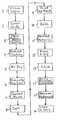
- FIG. 1is a flow chart showing the steps of one process of making a chip of the present invention.
- FIG. 2shows the parameters of the hydrophobic coat process.
- FIG. 3shows the parameters of etching the pad areas to the oxide wafer.
- FIG. 4shows a cross section of a chip made in accordance with the process of FIG. 1 and with the pad area etched to the oxide.
- the preferred embodiment of the process of the present inventionstarts with an 8-inch silicon wafer, polished on one side with the thickness of 725 ⁇ 25 ⁇ m in step 1 of FIG. 1.
- step 2the wafers are placed in a high temperature diffusion furnace such as a THERMCO and oxidized to produce a thermal oxide of 1000 ⁇ to 20,000 ⁇ .
- a thermal oxide of 3060 ⁇ 60 ⁇is produced at a temperature of 1,000° C. and a gas ratio H 2 O 2 1.8:1 with a specific preferred blue color.
- a hydrophobic fluorene polymer coatingis applied in step 3 .
- the preferred coatingis Cytonix made by Cytonix Corp. of Beltsville, Md.
- the Cytonix coatingis applied such as by using a SVG 90 track (Ser. #5209 CAB-08).
- the target thicknessmay be 300 ⁇ (post-bake) but preferably is reduced in step 4 to about 100 ⁇ and air-dried in step 5 before the bake cycle.
- the next Cytonix bake/cure stepis accomplished such as using SVG90 track (5209 CAB-08) at 200° C.
- the waferis positioned in proximity such as 10 millimeters from and not in contact with the baking plate as step 6 , and incrementally lowered to full contact followed by total bake time of 15 minutes in step 7 .
- the proximity placement and incremental loweringavoids wafer film anomalies and produces a more esthetic appearance.
- the parameters of the coating step 3 and baking step 4are shown in FIG. 2 where the exhaust is measured in liters/hour.
- a disposable “one-time use chip”is produced. This portion of the process and the product are illustrated in FIGS. 3 - 4 . This process and the product produced thereby increases the hydrophobicity delta between the analysis pad and the field area over the prior art.
- step 9the photo-resist is printed such as on an UltraTech 2150 XLS Stepper using the positive resist process and positive develop process shown in FIG. 3 by post exposure bake using MTI FlexFab (62-E1-2453) and development such as using a Shipley MF-701 developer followed by a rinse and dry in step 12 .
- the etch step designated 13removes just the hydrophobic Cytonix coating from the “open” analysis pad area, such as by using a barrel or single wafer etch chamber with CF4/02 gas. This results in a one time use chip with the hydrophobic field area exhibiting contacting angles of greater than 110° and the hydrophilic analysis pad verified to measure less than 50° (after removal of the photoresist).
- FIG. 4shows a cross-sectional view of the disk produced by the process including the silicon wafer 31 , oxide layer 32 and the hydrophobic field 33 and with the pads 34 extending down to the oxide layer 32 .
- step 14The hydrophobicity of the Cytonix coated (oxidized) wafer is verified in step 14 by depositing several droplets of deionized water onto the wafer surface.
- the repellant (contact) angleshould measure greater than 110 degrees.
- step 15the photo-resist is removed in step 15 and the wafer sliced and diced in step 16 .
Landscapes
- Chemical & Material Sciences (AREA)
- Health & Medical Sciences (AREA)
- Chemical Kinetics & Catalysis (AREA)
- Organic Chemistry (AREA)
- Analytical Chemistry (AREA)
- General Health & Medical Sciences (AREA)
- Hematology (AREA)
- Clinical Laboratory Science (AREA)
- Testing Or Measuring Of Semiconductors Or The Like (AREA)
- Sampling And Sample Adjustment (AREA)
Abstract
Description
- This application is based on and claims priority from provisional application Serial No. 60/247,325 filed Nov. 10, 2001.[0001]
- The present invention is directed to a product in the form of a chip for functional genomics for DNA testing and which holds or carries DNA samples and the method of making same. A preferred chip would have a hydrophobic field and hydrophilic pads within the field to hold the DNA.[0002]
- Attempts to manufacture a chip of this type for functional genomics by plasma dispositions and not requiring silation of the fields could produce the hydrophobic field but proved to be unstable, non-repeatable and resulted in a low yielding and poor quality of product.[0003]
- With the present invention, it has been possible to produce a hydrophobic fluorene polymer coated wafer with exceptional characteristics. The process of the present invention eradicates the instability and variability of organic pads, eliminates the need to alter the surface of previously produced chips via vapor silation methodology prior to depositing matrix and analyte and increases the hydrophobicity delta between field areas and silicon pad analysis areas.[0004]
- FIG. 1 is a flow chart showing the steps of one process of making a chip of the present invention.[0005]
- FIG. 2 shows the parameters of the hydrophobic coat process.[0006]
- FIG. 3 shows the parameters of etching the pad areas to the oxide wafer.[0007]
- FIG. 4 shows a cross section of a chip made in accordance with the process of FIG. 1 and with the pad area etched to the oxide.[0008]
- Referring now to FIG. 1, the preferred embodiment of the process of the present invention starts with an 8-inch silicon wafer, polished on one side with the thickness of 725±25 μm in[0009]
step 1 of FIG. 1. - In[0010]
step 2, the wafers are placed in a high temperature diffusion furnace such as a THERMCO and oxidized to produce a thermal oxide of 1000 Å to 20,000 Å. In the preferred embodiment of the invention a thermal oxide of 3060 ű60 Å is produced at a temperature of 1,000° C. and a gas ratio H2O21.8:1 with a specific preferred blue color. - If it is desired to place a legend, identifier or logo on the chip it can be performed in a fairly typical series of steps.[0011]
- Next a hydrophobic fluorene polymer coating is applied in[0012]
step 3. The preferred coating is Cytonix made by Cytonix Corp. of Beltsville, Md. The Cytonix coating is applied such as by using a SVG 90 track (Ser. #5209 CAB-08). The target thickness may be 300 Å (post-bake) but preferably is reduced instep 4 to about 100 Å and air-dried instep 5 before the bake cycle. - The next Cytonix bake/cure step is accomplished such as using SVG90 track (5209 CAB-08) at 200° C. Preferably, the wafer is positioned in proximity such as 10 millimeters from and not in contact with the baking plate as[0013]
step 6, and incrementally lowered to full contact followed by total bake time of 15 minutes instep 7. The proximity placement and incremental lowering avoids wafer film anomalies and produces a more esthetic appearance. The parameters of thecoating step 3 andbaking step 4 are shown in FIG. 2 where the exhaust is measured in liters/hour. - In accordance with the preferred embodiment of the present invention, a disposable “one-time use chip” is produced. This portion of the process and the product are illustrated in FIGS.[0014]3-4. This process and the product produced thereby increases the hydrophobicity delta between the analysis pad and the field area over the prior art.
- For masking and producing the desired number of pads, the wafers are coated and baked in steps[0015]8-11 and as shown in FIG. 3, such as on a MTI FlexFab (62-E1-2453) preferably using positive photo-resist with thick viscosity. The bulk thickness of positive photo-resist is reduced to less than 1.0 μm if the resist pads are used for matrix deposition by placing wafers in a developer solution that incrementally removes photo-resist material.
- In[0016]
step 9 the photo-resist is printed such as on an UltraTech 2150 XLS Stepper using the positive resist process and positive develop process shown in FIG. 3 by post exposure bake using MTI FlexFab (62-E1-2453) and development such as using a Shipley MF-701 developer followed by a rinse and dry instep 12. - In this process, the etch step designated[0017]13 removes just the hydrophobic Cytonix coating from the “open” analysis pad area, such as by using a barrel or single wafer etch chamber with CF4/02 gas. This results in a one time use chip with the hydrophobic field area exhibiting contacting angles of greater than 110° and the hydrophilic analysis pad verified to measure less than 50° (after removal of the photoresist).
- FIG. 4 shows a cross-sectional view of the disk produced by the process including the[0018]
silicon wafer 31,oxide layer 32 and thehydrophobic field 33 and with thepads 34 extending down to theoxide layer 32. - The hydrophobicity of the Cytonix coated (oxidized) wafer is verified in[0019]
step 14 by depositing several droplets of deionized water onto the wafer surface. The repellant (contact) angle should measure greater than 110 degrees. Finally the photo-resist is removed instep 15 and the wafer sliced and diced instep 16.
Claims (7)
1. A chip for functional genomics for DNA testing and which holds DNA samples comprising, in combination:
a silicon base,
an oxide layer on the base, and
a hydrophobic fluorene polymer coating on said oxide layer,
said coating having openings therethrough down to said oxide layer for holding DNA samples.
2. The chips ofclaim 1 wherein said coating is substantially 100 Å.
3. The chip ofclaim 1 wherein said openings in said coating have been formed using a positive photoresist.
4. The method of forming a chip from a silicon substrate for holding DNA samples comprising the steps of:
forming an oxide layer on the substrate,
forming a hydrophobic fluorene polymer coating on said substrate, and
etching away said coating down to said oxide layer in spaced apart positions to hold separate samples.
5. The method ofclaim 4 wherein said step of forming said coating includes the steps of applying a coating of said polymer on said oxide layer and positioning said polymer coated surface of said substrate close to but not in contact with a baking plate, incrementally moving said coated surface and baking plate into full contact and holding the contact to bake the polymer coating on said oxide layer.
6. The method ofclaim 4 wherein said etching step includes a positive resist process.
7. The method ofclaim 5 wherein said etching step includes a positive resist process.
Priority Applications (1)
| Application Number | Priority Date | Filing Date | Title |
|---|---|---|---|
| US10/008,185US20020146725A1 (en) | 2000-11-10 | 2001-11-09 | Chip for large-scale use of industrial genomics in health and agriculture and method of making same |
Applications Claiming Priority (2)
| Application Number | Priority Date | Filing Date | Title |
|---|---|---|---|
| US24732500P | 2000-11-10 | 2000-11-10 | |
| US10/008,185US20020146725A1 (en) | 2000-11-10 | 2001-11-09 | Chip for large-scale use of industrial genomics in health and agriculture and method of making same |
Publications (1)
| Publication Number | Publication Date |
|---|---|
| US20020146725A1true US20020146725A1 (en) | 2002-10-10 |
Family
ID=26677903
Family Applications (1)
| Application Number | Title | Priority Date | Filing Date |
|---|---|---|---|
| US10/008,185AbandonedUS20020146725A1 (en) | 2000-11-10 | 2001-11-09 | Chip for large-scale use of industrial genomics in health and agriculture and method of making same |
Country Status (1)
| Country | Link |
|---|---|
| US (1) | US20020146725A1 (en) |
Cited By (9)
| Publication number | Priority date | Publication date | Assignee | Title |
|---|---|---|---|---|
| US20040261703A1 (en)* | 2003-06-27 | 2004-12-30 | Jeffrey D. Chinn | Apparatus and method for controlled application of reactive vapors to produce thin films and coatings |
| US20050271809A1 (en)* | 2004-06-04 | 2005-12-08 | Boris Kobrin | Controlled deposition of silicon-containing coatings adhered by an oxide layer |
| US20050271900A1 (en)* | 2004-06-04 | 2005-12-08 | Boris Kobrin | Controlled vapor deposition of multilayered coatings adhered by an oxide layer |
| US20050271810A1 (en)* | 2004-06-04 | 2005-12-08 | Boris Kobrin | High aspect ratio performance coatings for biological microfluidics |
| US20060088666A1 (en)* | 2004-06-04 | 2006-04-27 | Applied Microstructures, Inc. | Controlled vapor deposition of biocompatible coatings over surface-treated substrates |
| US20060213441A1 (en)* | 2003-06-27 | 2006-09-28 | Applied Microstructures, Inc. | Apparatus and method for controlled application of reactive vapors to produce thin films and coatings |
| US20070020392A1 (en)* | 2004-06-04 | 2007-01-25 | Applied Microstructures, Inc. | Functional organic based vapor deposited coatings adhered by an oxide layer |
| GB2465906A (en)* | 2005-08-17 | 2010-06-09 | Waters Investments Ltd | Device for performing ionization desorption |
| US8987029B2 (en) | 2006-06-05 | 2015-03-24 | Applied Microstructures, Inc. | Protective thin films for use during fabrication of semiconductors, MEMS, and microstructures |
- 2001
- 2001-11-09USUS10/008,185patent/US20020146725A1/ennot_activeAbandoned
Cited By (20)
| Publication number | Priority date | Publication date | Assignee | Title |
|---|---|---|---|---|
| US20060213441A1 (en)* | 2003-06-27 | 2006-09-28 | Applied Microstructures, Inc. | Apparatus and method for controlled application of reactive vapors to produce thin films and coatings |
| US20050109277A1 (en)* | 2003-06-27 | 2005-05-26 | Boris Kobrin | Method for controlled application of reactive vapors to produce thin films and coatings |
| US10900123B2 (en)* | 2003-06-27 | 2021-01-26 | Spts Technologies Limited | Apparatus and method for controlled application of reactive vapors to produce thin films and coatings |
| US20170335455A1 (en)* | 2003-06-27 | 2017-11-23 | Spts Technologies Ltd. | Apparatus and method for controlled application of reactive vapors to produce thin films and coatings |
| US9725805B2 (en) | 2003-06-27 | 2017-08-08 | Spts Technologies Limited | Apparatus and method for controlled application of reactive vapors to produce thin films and coatings |
| US20040261703A1 (en)* | 2003-06-27 | 2004-12-30 | Jeffrey D. Chinn | Apparatus and method for controlled application of reactive vapors to produce thin films and coatings |
| US7413774B2 (en) | 2003-06-27 | 2008-08-19 | Applied Microstructures, Inc. | Method for controlled application of reactive vapors to produce thin films and coatings |
| US20050271893A1 (en)* | 2004-06-04 | 2005-12-08 | Applied Microstructures, Inc. | Controlled vapor deposition of multilayered coatings adhered by an oxide layer |
| US20070020392A1 (en)* | 2004-06-04 | 2007-01-25 | Applied Microstructures, Inc. | Functional organic based vapor deposited coatings adhered by an oxide layer |
| US20080026146A1 (en)* | 2004-06-04 | 2008-01-31 | Applied Microstrctures, Inc. | Method of depositing a multilayer coating with a variety of oxide adhesion layers and organic layers |
| US20060088666A1 (en)* | 2004-06-04 | 2006-04-27 | Applied Microstructures, Inc. | Controlled vapor deposition of biocompatible coatings over surface-treated substrates |
| US7638167B2 (en) | 2004-06-04 | 2009-12-29 | Applied Microstructures, Inc. | Controlled deposition of silicon-containing coatings adhered by an oxide layer |
| US7695775B2 (en) | 2004-06-04 | 2010-04-13 | Applied Microstructures, Inc. | Controlled vapor deposition of biocompatible coatings over surface-treated substrates |
| US7776396B2 (en) | 2004-06-04 | 2010-08-17 | Applied Microstructures, Inc. | Controlled vapor deposition of multilayered coatings adhered by an oxide layer |
| US7879396B2 (en) | 2004-06-04 | 2011-02-01 | Applied Microstructures, Inc. | High aspect ratio performance coatings for biological microfluidics |
| US20050271810A1 (en)* | 2004-06-04 | 2005-12-08 | Boris Kobrin | High aspect ratio performance coatings for biological microfluidics |
| US20050271900A1 (en)* | 2004-06-04 | 2005-12-08 | Boris Kobrin | Controlled vapor deposition of multilayered coatings adhered by an oxide layer |
| US20050271809A1 (en)* | 2004-06-04 | 2005-12-08 | Boris Kobrin | Controlled deposition of silicon-containing coatings adhered by an oxide layer |
| GB2465906A (en)* | 2005-08-17 | 2010-06-09 | Waters Investments Ltd | Device for performing ionization desorption |
| US8987029B2 (en) | 2006-06-05 | 2015-03-24 | Applied Microstructures, Inc. | Protective thin films for use during fabrication of semiconductors, MEMS, and microstructures |
Similar Documents
| Publication | Publication Date | Title |
|---|---|---|
| US6787339B1 (en) | Microfluidic devices having embedded metal conductors and methods of fabricating said devices | |
| US20020146725A1 (en) | Chip for large-scale use of industrial genomics in health and agriculture and method of making same | |
| CA2449193A1 (en) | Method of manufacturing a microfluidic structure, in particular a biochip, and structure obtained by said method | |
| CN112645276A (en) | Indium column and preparation method thereof | |
| JPH02266517A (en) | Manufacture of semiconductor device | |
| JPH02267967A (en) | Manufacture of semiconductor element | |
| JP2002110654A (en) | Method of manufacturing semiconductor device | |
| JP2003139920A (en) | Method of manufacturing microlens | |
| JPS63133629A (en) | Manufacture of integrated circuit device | |
| JPH06295877A (en) | Formation of contact hole in semiconductor device | |
| JPS5893270A (en) | Manufacture of semiconductor device | |
| JP2000221161A (en) | Production of integrated sensor array | |
| JPH1180974A (en) | Method for measuring etching rate | |
| JPS6236827A (en) | Method for selective etching | |
| JPH0876352A (en) | Formation of pattern | |
| JPH04364726A (en) | Pattern formation method | |
| JP3815413B2 (en) | Manufacturing method of semiconductor device | |
| KR0151294B1 (en) | Method of manufacturing field effect transistor | |
| KR100734664B1 (en) | Fine pattern formation method using the orientation principle of the Langmuir blowjet film | |
| JP2912002B2 (en) | Method for manufacturing semiconductor device | |
| JPS59171124A (en) | Method for burying photoresist film | |
| JPS6153726A (en) | Pattern formation | |
| JP3149601B2 (en) | Method for forming contact hole in semiconductor device | |
| KR930006133B1 (en) | Contact hole formation method of MOS device | |
| JPH07161721A (en) | Method of flattening thick film resist |
Legal Events
| Date | Code | Title | Description |
|---|---|---|---|
| AS | Assignment | Owner name:TACTICAL FABS, INC., CALIFORNIA Free format text:ASSIGNMENT OF ASSIGNORS INTEREST;ASSIGNORS:MULLEN, BETTE M.;MAY, JEFFREY L.;REEL/FRAME:012961/0821 Effective date:20020514 | |
| STCB | Information on status: application discontinuation | Free format text:ABANDONED -- FAILURE TO RESPOND TO AN OFFICE ACTION |