US20020142531A1 - Dual damascene copper gate and interconnect therefore - Google Patents
Dual damascene copper gate and interconnect thereforeDownload PDFInfo
- Publication number
- US20020142531A1 US20020142531A1US09/821,210US82121001AUS2002142531A1US 20020142531 A1US20020142531 A1US 20020142531A1US 82121001 AUS82121001 AUS 82121001AUS 2002142531 A1US2002142531 A1US 2002142531A1
- Authority
- US
- United States
- Prior art keywords
- layer
- gate
- depositing
- barrier metal
- metal layer
- Prior art date
- Legal status (The legal status is an assumption and is not a legal conclusion. Google has not performed a legal analysis and makes no representation as to the accuracy of the status listed.)
- Abandoned
Links
- RYGMFSIKBFXOCR-UHFFFAOYSA-NCopperChemical compound[Cu]RYGMFSIKBFXOCR-UHFFFAOYSA-N0.000titleclaimsabstractdescription16
- 229910052802copperInorganic materials0.000titleclaimsabstractdescription16
- 239000010949copperSubstances0.000titleclaimsabstractdescription16
- 230000009977dual effectEffects0.000titleclaimsabstractdescription15
- 229910052751metalInorganic materials0.000claimsabstractdescription71
- 239000002184metalSubstances0.000claimsabstractdescription71
- 230000004888barrier functionEffects0.000claimsabstractdescription45
- 238000000034methodMethods0.000claimsabstractdescription41
- 238000000151depositionMethods0.000claimsabstractdescription37
- 238000005530etchingMethods0.000claimsabstractdescription14
- XUIMIQQOPSSXEZ-UHFFFAOYSA-NSiliconChemical compound[Si]XUIMIQQOPSSXEZ-UHFFFAOYSA-N0.000claimsabstractdescription7
- 229910052710siliconInorganic materials0.000claimsabstractdescription7
- 239000010703siliconSubstances0.000claimsabstractdescription7
- 239000000758substrateSubstances0.000claimsabstractdescription6
- 239000004065semiconductorSubstances0.000claimsabstractdescription5
- 229910052581Si3N4Inorganic materials0.000claimsdescription12
- ATJFFYVFTNAWJD-UHFFFAOYSA-NTinChemical compound[Sn]ATJFFYVFTNAWJD-UHFFFAOYSA-N0.000claimsdescription8
- 150000002739metalsChemical class0.000claimsdescription7
- 229910004200TaSiNInorganic materials0.000claimsdescription5
- RTAQQCXQSZGOHL-UHFFFAOYSA-NTitaniumChemical compound[Ti]RTAQQCXQSZGOHL-UHFFFAOYSA-N0.000claimsdescription5
- MCMNRKCIXSYSNV-UHFFFAOYSA-NZirconium dioxideChemical compoundO=[Zr]=OMCMNRKCIXSYSNV-UHFFFAOYSA-N0.000claimsdescription4
- 229910021420polycrystalline siliconInorganic materials0.000claimsdescription4
- 229920005591polysiliconPolymers0.000claimsdescription4
- CJNBYAVZURUTKZ-UHFFFAOYSA-Nhafnium(IV) oxideInorganic materialsO=[Hf]=OCJNBYAVZURUTKZ-UHFFFAOYSA-N0.000claimsdescription2
- HQVNEWCFYHHQES-UHFFFAOYSA-Nsilicon nitrideChemical compoundN12[Si]34N5[Si]62N3[Si]51N64HQVNEWCFYHHQES-UHFFFAOYSA-N0.000claims11
- 239000000463materialSubstances0.000claims6
- 150000004767nitridesChemical class0.000description12
- 230000008569processEffects0.000description10
- 238000004519manufacturing processMethods0.000description7
- 230000015572biosynthetic processEffects0.000description5
- 238000005755formation reactionMethods0.000description5
- -1boron ionsChemical class0.000description3
- 238000005516engineering processMethods0.000description3
- XKRFYHLGVUSROY-UHFFFAOYSA-NArgonChemical compound[Ar]XKRFYHLGVUSROY-UHFFFAOYSA-N0.000description2
- 229910052785arsenicInorganic materials0.000description2
- 229910052796boronInorganic materials0.000description2
- 238000005468ion implantationMethods0.000description2
- 229920002120photoresistant polymerPolymers0.000description2
- 238000004544sputter depositionMethods0.000description2
- 229910052724xenonInorganic materials0.000description2
- FHNFHKCVQCLJFQ-UHFFFAOYSA-Nxenon atomChemical compound[Xe]FHNFHKCVQCLJFQ-UHFFFAOYSA-N0.000description2
- ZOXJGFHDIHLPTG-UHFFFAOYSA-NBoronChemical compound[B]ZOXJGFHDIHLPTG-UHFFFAOYSA-N0.000description1
- 241000536399TinaSpecies0.000description1
- 229910052786argonInorganic materials0.000description1
- 230000008021depositionEffects0.000description1
- 239000003989dielectric materialSubstances0.000description1
- 238000002513implantationMethods0.000description1
- 230000006872improvementEffects0.000description1
- 239000012212insulatorSubstances0.000description1
- 150000002500ionsChemical class0.000description1
- 238000002955isolationMethods0.000description1
- 230000000873masking effectEffects0.000description1
- 238000001465metallisationMethods0.000description1
- 230000004048modificationEffects0.000description1
- 238000012986modificationMethods0.000description1
- 230000003647oxidationEffects0.000description1
- 238000007254oxidation reactionMethods0.000description1
- 230000035515penetrationEffects0.000description1
- 238000002294plasma sputter depositionMethods0.000description1
- 238000005498polishingMethods0.000description1
- GUVRBAGPIYLISA-UHFFFAOYSA-Ntantalum atomChemical compound[Ta]GUVRBAGPIYLISA-UHFFFAOYSA-N0.000description1
- 238000001039wet etchingMethods0.000description1
Images


Classifications
- H—ELECTRICITY
- H01—ELECTRIC ELEMENTS
- H01L—SEMICONDUCTOR DEVICES NOT COVERED BY CLASS H10
- H01L21/00—Processes or apparatus adapted for the manufacture or treatment of semiconductor or solid state devices or of parts thereof
- H01L21/02—Manufacture or treatment of semiconductor devices or of parts thereof
- H01L21/04—Manufacture or treatment of semiconductor devices or of parts thereof the devices having potential barriers, e.g. a PN junction, depletion layer or carrier concentration layer
- H01L21/18—Manufacture or treatment of semiconductor devices or of parts thereof the devices having potential barriers, e.g. a PN junction, depletion layer or carrier concentration layer the devices having semiconductor bodies comprising elements of Group IV of the Periodic Table or AIIIBV compounds with or without impurities, e.g. doping materials
- H—ELECTRICITY
- H10—SEMICONDUCTOR DEVICES; ELECTRIC SOLID-STATE DEVICES NOT OTHERWISE PROVIDED FOR
- H10D—INORGANIC ELECTRIC SEMICONDUCTOR DEVICES
- H10D64/00—Electrodes of devices having potential barriers
- H10D64/01—Manufacture or treatment
- H10D64/017—Manufacture or treatment using dummy gates in processes wherein at least parts of the final gates are self-aligned to the dummy gates, i.e. replacement gate processes
- H—ELECTRICITY
- H01—ELECTRIC ELEMENTS
- H01L—SEMICONDUCTOR DEVICES NOT COVERED BY CLASS H10
- H01L21/00—Processes or apparatus adapted for the manufacture or treatment of semiconductor or solid state devices or of parts thereof
- H01L21/70—Manufacture or treatment of devices consisting of a plurality of solid state components formed in or on a common substrate or of parts thereof; Manufacture of integrated circuit devices or of parts thereof
- H01L21/71—Manufacture of specific parts of devices defined in group H01L21/70
- H01L21/768—Applying interconnections to be used for carrying current between separate components within a device comprising conductors and dielectrics
Definitions
- This inventionrelates to CMOS Integrated circuits, and specifically to the formation, in a single process step, of a metal gate and a metal interconnect therefore.
- a metal gate structuresuch as polysilicon replacement gate, nitride replacement gate, or use of a TiN, W, or Mo gate.
- a metal gatehas the advantages of providing high-speed switching, and does not allow boron penetration into the underlying silicon substrate.
- the known metal gate formations techniquesare complex processes, which require additional masking, etching and deposition, resulting in a very high fabrication cost when used in the manufacturing process.
- a method of forming a semiconductor device having a simultaneously formed gate and interconnecttherefore, includes preparing a silicon substrate, including isolating active areas thereon; forming an insulating layer in a gate region of an active area; depositing a first barrier metal layer; depositing a gate place-holder layer on the first barrier metal layer; etching the gate place-holder layer and the first barrier metal layer to form a gate stack; building an oxide sidewall about the gate stack; forming a source region and a drain region in the active area; depositing an oxide layer over the structure and etching the oxide layer to form a dual damascene trench to the level of the gate place-holder and to form vias for the source region and drain region; removing the gate place-holder; depositing a second barrier metal layer; depositing copper into the dual damascene trench and the vias; and removing excess copper and all portions of the second barrier metal layer to the level of the last deposited oxide layer.
- An object of the inventionis to provide a low cost metal gate fabrication technology.
- Another object of the inventionis to provide a method of fabricating a metal gate and a first level interconnect in a single process step.
- FIGS. 1 - 5depict successive steps in forming a dual damascene copper gate and metal interconnect according to the method of the invention.
- the method of the inventionprovides a technique for the fabrication of a metal gate and an interconnect therefore in a single process step.
- the method of the inventionalso provides for simultaneous fabrication of metal interconnects for a source and drain at the same time as forming the gate interconnect.
- a replacement gate processmay complete the front-end process.
- a nitride replacementis used as an example. This is a low cost process, whose utility will be apparent to those of ordinary skill in the art.
- a bulk silicon wafer 10is segmented to provide device isolation by oxide regions 12 and to form device areas, one of which is shown generally at 14 .
- a p-well 16is formed implantation of boron ions, at a dose of about 5 ⁇ 10 13 cm ⁇ 2 to 5 ⁇ 10 14 cm ⁇ 2 , and at an energy level of 20 keV to 100 keV.
- the threshold voltageis adjusted.
- An insulating layerwhich in the preferred embodiment is a gate oxide layer 18 , is formed by thermal oxidation.
- the gate oxidemay be replaced with any high-k gate dielectric material, such as HfO 2 or ZrO 2 .
- a first, or lower, barrier metal layer 20is deposited to a thickness of between about 5 nm to 20 nm.
- the barrier metalis the component which determines the flat band voltage, and therefore, controls the threshold voltage of the device.
- the first barrier metalmay not be required if the wet nitride will not degrade the gate insulator reliability.
- the first barrier metalmay be any of TiN, TaN, WN, TiTaN, and TaSiN, as well as other suitable barrier metals.
- a nitride layer(Si 3 N 4 ) is deposited by CVD. Photoresist is applied and the nitride etched to form a nitride sacrificial gate 22 , also referred to herein as a gate place-holder, having a thickness of between about 100 nm and 300 nm. Barrier metal layer 20 is also etched in this step to form a nitride/barrier metal gate stack.
- LDD ion implantatione.g., LDD of arsenic ions, at a dose of 5 ⁇ 10 13 cm ⁇ 2 to 5 ⁇ 10 14 cm ⁇ 2 , and at an energy level of 10 keV to 30 keV, resulting in the structure of FIG. 1.
- An oxide layeris deposited by CVD. This oxide layer is plasma etched to form an oxide side wall 28 about nitride gate 22 .
- An N+ source and drainare formed by ion implantation, for example of arsenic ions at a dose of about 1 ⁇ 10 15 cm ⁇ 2 to 5 ⁇ 10 15 cm ⁇ 2 , and at an energy level of 30 keV to 60 keV, resulting in the structure of FIG. 2.
- the source and drain, for a PMOS,may also be formed using P+ ions. The forgoing process steps are similar to those disclosed in the above-identified related application.
- Additional oxide 34is deposited by CVD and planarize by CMP to smooth the upper surface of the structure.
- the thickness of remaining oxideis about the same as the combined height of sacrificial nitride gate 22 and the thickness of first metal layer 20 .
- Photoresistis applied prior to etching to form of a dual damascene trench 36 and vias.
- Complete Dual Damascenesincluding the trenches to the first metal layer and the vias, are formed for a source 38 and drain 40 contacts.
- One trench 36is provided to the gate interconnect. Forming the gate interconnect trench exposes the upper surface of nitride gate 22 , resulting in the structure of FIG. 3.
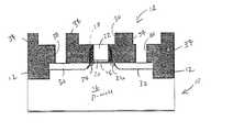
- Nitride gate 22is removed by wet etching, and a second, or upper, barrier metal layer 42 is deposited for copper interconnects, as shown in FIG. 4.
- the second barrier metal layermay be formed of any of the metals identified for the first barrier metal layer, however, it is preferred that the same metal be used for both the first and second barrier metal layers.
- Copperis deposited and polished by CMP to delineate a gate copper interconnect 44 , 46 , 48 , to connect source 30 and drain 32 , respectively, and to remove that portion of second barrier metal layer 42 from the top surface of oxide 34 , as is shown in FIG. 5.
- the metal gateis formed at the same time as the source/drain interconnect, and saves one metal deposition and one CMP step from the conventional metal gate process.
- the method of the inventionmay easily be adapted to the formation of a single Damascene process, wherein the gate electrode and the source and drain via contacts are formed without the requirement of depositing the first interconnect metal.
Landscapes
- Engineering & Computer Science (AREA)
- Physics & Mathematics (AREA)
- Condensed Matter Physics & Semiconductors (AREA)
- General Physics & Mathematics (AREA)
- Manufacturing & Machinery (AREA)
- Computer Hardware Design (AREA)
- Microelectronics & Electronic Packaging (AREA)
- Power Engineering (AREA)
- Insulated Gate Type Field-Effect Transistor (AREA)
- Internal Circuitry In Semiconductor Integrated Circuit Devices (AREA)
- Electrodes Of Semiconductors (AREA)
Abstract
Description
- This application is related to U.S. Pat. No. 6,133,106, granted Oct. 17, 2000, to Evans et al., for[0001]Fabrication of a planar MOSFET with raised source/drain by chemical mechanical polishing and nitride replacement.
- This invention relates to CMOS Integrated circuits, and specifically to the formation, in a single process step, of a metal gate and a metal interconnect therefore.[0002]
- There are many techniques known in the art for forming a metal gate structure, such as polysilicon replacement gate, nitride replacement gate, or use of a TiN, W, or Mo gate. A metal gate has the advantages of providing high-speed switching, and does not allow boron penetration into the underlying silicon substrate. The known metal gate formations techniques, however, are complex processes, which require additional masking, etching and deposition, resulting in a very high fabrication cost when used in the manufacturing process.[0003]
- H. Yang et al,[0004]A comparison of TiN processes for CVD W/TiNgate electrode on3nm gate oxide,IEDM-97, pp459-462, 1997, describes use of TiN as a gate electrode and various techniques for forming such a gate electrode.
- A. Chatterjee et al.,[0005]Sub-100nm gate length metal gate NMOS transistors fabricated by a replacement gate process,IEDM-97, pp821-824, 1997, describes use of a polysilicon gate place-holder, and subsequent replacement of such place-holder by a metal.
- J. C. Hu et al,[0006]Feasability of using W/TiNas metal gate for conventional0.13μm CMOS technology and beyond,IEDM-97, pp825-828, 1997, describes techniques for using W/TiN as a metal gate.
- T. Ushiki et al.,[0007]Improvement of gate oxide reliability for tantalum-gate MOS devices using xenon plasma sputtering technology,IEEE Transactions on Electronic Devices, Vol. 45, No. 11, pp2349-2354, November 1998, describes advantages of xenon sputtering over argon sputtering.
- A method of forming a semiconductor device having a simultaneously formed gate and interconnect therefore, includes preparing a silicon substrate, including isolating active areas thereon; forming an insulating layer in a gate region of an active area; depositing a first barrier metal layer; depositing a gate place-holder layer on the first barrier metal layer; etching the gate place-holder layer and the first barrier metal layer to form a gate stack; building an oxide sidewall about the gate stack; forming a source region and a drain region in the active area; depositing an oxide layer over the structure and etching the oxide layer to form a dual damascene trench to the level of the gate place-holder and to form vias for the source region and drain region; removing the gate place-holder; depositing a second barrier metal layer; depositing copper into the dual damascene trench and the vias; and removing excess copper and all portions of the second barrier metal layer to the level of the last deposited oxide layer.[0008]
- An object of the invention is to provide a low cost metal gate fabrication technology.[0009]
- Another object of the invention is to provide a method of fabricating a metal gate and a first level interconnect in a single process step.[0010]
- This summary and objectives of the invention are provided to enable quick comprehension of the nature of the invention. A more thorough understanding of the invention may be obtained by reference to the following detailed description of the preferred embodiment of the invention in connection with the drawings.[0011]
- FIGS.[0012]1-5 depict successive steps in forming a dual damascene copper gate and metal interconnect according to the method of the invention.
- The method of the invention provides a technique for the fabrication of a metal gate and an interconnect therefore in a single process step. The method of the invention also provides for simultaneous fabrication of metal interconnects for a source and drain at the same time as forming the gate interconnect. A replacement gate process may complete the front-end process. A nitride replacement is used as an example. This is a low cost process, whose utility will be apparent to those of ordinary skill in the art.[0013]
- State of the art process are followed for well formation, threshold voltage adjustment, and STI formation. By way of example, and now referring to FIG. 1, a[0014]
bulk silicon wafer 10 is segmented to provide device isolation byoxide regions 12 and to form device areas, one of which is shown generally at14. A p-well 16 is formed implantation of boron ions, at a dose of about 5·1013cm−2to 5·1014cm−2, and at an energy level of 20 keV to 100 keV. The threshold voltage is adjusted. An insulating layer, which in the preferred embodiment is agate oxide layer 18, is formed by thermal oxidation. The gate oxide may be replaced with any high-k gate dielectric material, such as HfO2or ZrO2. - A first, or lower,[0015]
barrier metal layer 20 is deposited to a thickness of between about 5 nm to 20 nm. The barrier metal is the component which determines the flat band voltage, and therefore, controls the threshold voltage of the device. The first barrier metal may not be required if the wet nitride will not degrade the gate insulator reliability. The first barrier metal may be any of TiN, TaN, WN, TiTaN, and TaSiN, as well as other suitable barrier metals. - A nitride layer (Si[0016]3N4) is deposited by CVD. Photoresist is applied and the nitride etched to form a nitride
sacrificial gate 22, also referred to herein as a gate place-holder, having a thickness of between about 100 nm and 300 nm.Barrier metal layer 20 is also etched in this step to form a nitride/barrier metal gate stack. LDD ion implantation, e.g., LDD of arsenic ions, at a dose of 5·1013cm−2to 5·1014cm−2, and at an energy level of 10 keV to 30 keV, resulting in the structure of FIG. 1. - An oxide layer is deposited by CVD. This oxide layer is plasma etched to form an[0017]
oxide side wall 28 aboutnitride gate 22. An N+ source and drain are formed by ion implantation, for example of arsenic ions at a dose of about 1·1015cm−2to 5·1015cm−2, and at an energy level of 30 keV to 60 keV, resulting in the structure of FIG. 2. The source and drain, for a PMOS, may also be formed using P+ ions. The forgoing process steps are similar to those disclosed in the above-identified related application. - [0018]
Additional oxide 34 is deposited by CVD and planarize by CMP to smooth the upper surface of the structure. The thickness of remaining oxide is about the same as the combined height ofsacrificial nitride gate 22 and the thickness offirst metal layer 20. - Photoresist is applied prior to etching to form of a dual[0019]
damascene trench 36 and vias. Complete Dual Damascenes, including the trenches to the first metal layer and the vias, are formed for a source38 and drain40 contacts. Onetrench 36 is provided to the gate interconnect. Forming the gate interconnect trench exposes the upper surface ofnitride gate 22, resulting in the structure of FIG. 3. - Nitride[0020]
gate 22 is removed by wet etching, and a second, or upper,barrier metal layer 42 is deposited for copper interconnects, as shown in FIG. 4. The second barrier metal layer may be formed of any of the metals identified for the first barrier metal layer, however, it is preferred that the same metal be used for both the first and second barrier metal layers. - Copper is deposited and polished by CMP to delineate a[0021]
gate copper interconnect source 30 anddrain 32, respectively, and to remove that portion of secondbarrier metal layer 42 from the top surface ofoxide 34, as is shown in FIG. 5. - As the above process demonstrates, the metal gate is formed at the same time as the source/drain interconnect, and saves one metal deposition and one CMP step from the conventional metal gate process. The method of the invention may easily be adapted to the formation of a single Damascene process, wherein the gate electrode and the source and drain via contacts are formed without the requirement of depositing the first interconnect metal.[0022]
- Thus, a method for forming a dual damascene copper gate and metal interconnect has been disclosed. It will be appreciated that further variations and modifications thereof may be made within the scope of the invention as defined in the appended claims.[0023]
Claims (15)
1. A method of forming a semiconductor device having a simultaneously formed gate and interconnect therefore, comprising:
preparing a silicon substrate, including isolating active areas thereon;
forming an insulating layer in a gate region of an active area;
depositing a first barrier metal layer;
depositing a gate place-holder layer on the first barrier metal layer;
etching the gate place-holder layer and the first barrier metal layer to form a gate stack;
building an oxide sidewall about the gate stack;
forming a source region and a drain region in the active area;
depositing an oxide layer over the structure and etching the oxide layer to form a dual damascene trench to the level of the gate place-holder and to form vias for the source region and drain region;
removing the gate place-holder;
depositing a second barrier metal layer;
depositing copper into the dual damascene trench and the vias; and
removing excess copper and all portions of the second barrier metal layer to the level of the last deposited oxide layer.
2. The method ofclaim 1 wherein said depositing a gate place-holder includes depositing a thin layer of material taken from the group of materials consisting of silicon nitride and polysilicon.
3. The method ofclaim 2 wherein said depositing a silicon nitride layer includes depositing the silicon nitride layer to a thickness of between about 100 nm to 300 nm.
4. The method ofclaim 1 wherein the first and second barrier metals are taken from the group of metals consisting of TiN, TaN, WN, TiTaN, and TaSiN.
5. The method ofclaim 4 wherein the first barrier metal layer is deposited to a thickness of between about 5 nm and 20 nm.
6. The method ofclaim 1 wherein said forming an insulating layer includes forming a gate oxide layer.
7. The method ofclaim 1 wherein said forming an insulating layer includes forming a layer of high-k material taken from the group of materials consisting of HfO2and ZrO2.
8. A method of forming a semiconductor device having a simultaneously formed gate and interconnect therefore, comprising:
preparing a silicon substrate, including isolating active areas thereon;
forming an insulating layer of a gate oxide in a gate region of an active area;
depositing a first barrier metal layer;
depositing a silicon nitride layer on the first barrier metal layer;
etching the silicon nitride layer and the first barrier metal layer to form a gate stack;
building an oxide sidewall about the gate stack;
forming a source region and a drain region in the active area;
depositing an oxide layer over the structure and etching the oxide layer to form a dual damascene trench to the level of the silicon nitride and to form vias for the source region and the drain region;
removing the silicon nitride;
depositing a second barrier metal layer, wherein the first barrier metal and the second barrier metal are taken from the group of metals consisting of TiN, TaN, WN, TiTaN, and TaSiN;
depositing copper into the dual damascene trench and the vias; and
removing excess copper and all portions of the second barrier metal layer to the level of the last deposited oxide layer.
9. The method ofclaim 8 wherein said depositing a silicon nitride layer includes depositing the silicon nitride layer to a thickness of between about 100 nm to 300 nm.
10. The method ofclaim 8 wherein the first barrier metal layer is deposited to a thickness of between about 5 nm and 20 nm.
11. A method of forming a semiconductor device having a simultaneously formed gate and interconnect therefore, comprising:
preparing a silicon substrate, including isolating active areas thereon;
forming an insulating layer of a gate oxide in a gate region of an active area;
depositing a gate place-holder layer on the first barrier metal layer, including depositing a thin layer of material taken from the group of materials consisting of silicon nitride and polysilicon;
etching the gate place-holder;
building an oxide sidewall about the gate place-holder;
forming a source region and a drain region in the active area;
depositing an oxide layer over the structure and etching the oxide layer to form a dual damascene trench to the level of the gate place-holder and to form vias for the source region and drain region;
removing the gate place-holder;
depositing an upper barrier metal layer;
depositing copper into the dual damascene trench and the vias; and
removing excess copper and all portions of the upper barrier metal layer to the level of the last deposited oxide layer.
12. The method ofclaim 11 wherein said depositing a gate place-holder layer includes depositing a silicon nitride layer to a thickness of between about 100 nm to 300 nm.
13. The method ofclaim 1 1 wherein the upper barrier metal is taken from the group of metals consisting of TiN, TaN, WN, TiTaN, and TaSiN.
14. The method ofclaim 11 which includes, prior to depositing said gate place-holder layer, depositing a lower barrier metal layer on the gate oxide, and wherein the first barrier metal layer is deposited to a thickness of between about 5 nm and 20 nm, and wherein said etching includes etching the gate place-holder layer and the lower barrier metal layer to form a gate stack..
15. The method ofclaim 14 wherein the lower barrier metal is taken from the group of metals consisting of TiN, TaN, WN, TiTaN, and TaSiN.
Priority Applications (4)
| Application Number | Priority Date | Filing Date | Title |
|---|---|---|---|
| US09/821,210US20020142531A1 (en) | 2001-03-29 | 2001-03-29 | Dual damascene copper gate and interconnect therefore |
| JP2002079751AJP2002329866A (en) | 2001-03-29 | 2002-03-20 | Copper gate by dual damascene method and its interconnect |
| TW091105998ATWI305008B (en) | 2001-03-29 | 2002-03-27 | Dual damascene copper gate and interconnect therefore |
| KR10-2002-0016829AKR100407385B1 (en) | 2001-03-29 | 2002-03-27 | Dual damascene copper gate and interconnet therefore |
Applications Claiming Priority (1)
| Application Number | Priority Date | Filing Date | Title |
|---|---|---|---|
| US09/821,210US20020142531A1 (en) | 2001-03-29 | 2001-03-29 | Dual damascene copper gate and interconnect therefore |
Publications (1)
| Publication Number | Publication Date |
|---|---|
| US20020142531A1true US20020142531A1 (en) | 2002-10-03 |
Family
ID=25232808
Family Applications (1)
| Application Number | Title | Priority Date | Filing Date |
|---|---|---|---|
| US09/821,210AbandonedUS20020142531A1 (en) | 2001-03-29 | 2001-03-29 | Dual damascene copper gate and interconnect therefore |
Country Status (4)
| Country | Link |
|---|---|
| US (1) | US20020142531A1 (en) |
| JP (1) | JP2002329866A (en) |
| KR (1) | KR100407385B1 (en) |
| TW (1) | TWI305008B (en) |
Cited By (29)
| Publication number | Priority date | Publication date | Assignee | Title |
|---|---|---|---|---|
| US20040164362A1 (en)* | 2003-01-15 | 2004-08-26 | Conley John F. | Reactive gate electrode conductive barrier |
| US20050051854A1 (en)* | 2003-09-09 | 2005-03-10 | International Business Machines Corporation | Structure and method for metal replacement gate of high performance |
| US20050287748A1 (en)* | 2004-06-24 | 2005-12-29 | Jack Kavalieros | Reducing reactions between polysilicon gate electrodes and high dielectric constant gate dielectrics |
| CN102214576A (en)* | 2010-04-09 | 2011-10-12 | 中国科学院微电子研究所 | Semiconductor device and method for manufacturing the same |
| CN102468174A (en)* | 2010-11-18 | 2012-05-23 | 中国科学院微电子研究所 | Semiconductor device and forming method thereof |
| US20120261829A1 (en)* | 2011-04-15 | 2012-10-18 | International Business Machines Corporation | Middle of line structures and methods for fabrication |
| US20120282765A1 (en)* | 2011-05-04 | 2012-11-08 | Globalfoundries Inc. | Method of Forming Metal Gates and Metal Contacts in a Common Fill Process |
| CN102779751A (en)* | 2011-05-11 | 2012-11-14 | 中国科学院微电子研究所 | Method for manufacturing semiconductor device |
| US20120289015A1 (en)* | 2011-05-13 | 2012-11-15 | United Microelectronics Corp. | Method for fabricating semiconductor device with enhanced channel stress |
| CN102983098A (en)* | 2011-09-07 | 2013-03-20 | 中国科学院微电子研究所 | Method for manufacturing electrode and connecting line in gate-last process |
| CN103296026A (en)* | 2012-02-22 | 2013-09-11 | 权义弼 | Nonvolatile memory device and method of fabricating the same |
| DE102013105608B3 (en)* | 2013-02-27 | 2014-02-13 | Taiwan Semiconductor Manufacturing Company, Ltd. | Integrated circuit (IC) structure for use in e.g. microprocessor, has continuous metallic portion that is formed between gate contact and metal |
| CN103855095A (en)* | 2012-12-04 | 2014-06-11 | 中芯国际集成电路制造(上海)有限公司 | Method for manufacturing semiconductor device |
| US8900988B2 (en) | 2011-04-15 | 2014-12-02 | International Business Machines Corporation | Method for forming self-aligned airgap interconnect structures |
| CN104241107A (en)* | 2013-06-06 | 2014-12-24 | 中国科学院微电子研究所 | Semiconductor structure and manufacturing method thereof |
| CN104269378A (en)* | 2014-09-24 | 2015-01-07 | 上海华力微电子有限公司 | Forming method of source electrode interconnection structure |
| US9054160B2 (en) | 2011-04-15 | 2015-06-09 | International Business Machines Corporation | Interconnect structure and method for fabricating on-chip interconnect structures by image reversal |
| CN104701150A (en)* | 2013-12-05 | 2015-06-10 | 中芯国际集成电路制造(上海)有限公司 | Transistor forming method |
| CN104867928A (en)* | 2015-04-30 | 2015-08-26 | 上海集成电路研发中心有限公司 | Preparation method of gate metals and contact hole metals in CMOS device |
| US9236298B2 (en) | 2011-09-08 | 2016-01-12 | Globalfoundries Inc. | Methods for fabrication interconnect structures with functional components and electrical conductive contact structures on a same level |
| US9299847B2 (en) | 2012-05-10 | 2016-03-29 | Globalfoundries Inc. | Printed transistor and fabrication method |
| US9530856B2 (en) | 2013-12-26 | 2016-12-27 | Semiconductor Energy Laboratory Co., Ltd. | Semiconductor device and method for manufacturing the same |
| US20170162711A1 (en)* | 2015-12-02 | 2017-06-08 | International Business Machines Corporation | Structure and process for overturned thin film device with self-aligned gate and s/d contacts |
| US9847355B2 (en) | 2002-05-17 | 2017-12-19 | Semiconductor Energy Laboratory Co., Ltd. | Silicon nitride film, and semiconductor device |
| WO2018039349A1 (en)* | 2016-08-24 | 2018-03-01 | Euipil Kwon | Nonvolatile memory device and method of fabricating the same |
| US10096550B2 (en) | 2017-02-21 | 2018-10-09 | Raytheon Company | Nitride structure having gold-free contact and methods for forming such structures |
| US10224285B2 (en) | 2017-02-21 | 2019-03-05 | Raytheon Company | Nitride structure having gold-free contact and methods for forming such structures |
| US11043454B2 (en) | 2019-01-17 | 2021-06-22 | Samsung Electronics Co., Ltd. | Low resistivity interconnects with doped barrier layer for integrated circuits |
| US11901426B2 (en)* | 2017-11-22 | 2024-02-13 | Taiwan Semiconductor Manufacturing Co., Ltd. | Forming metal contacts on metal gates |
Families Citing this family (3)
| Publication number | Priority date | Publication date | Assignee | Title |
|---|---|---|---|---|
| JP4647311B2 (en)* | 2002-12-09 | 2011-03-09 | アイメック | Method for forming dielectric stack |
| JP2005244186A (en)* | 2004-02-23 | 2005-09-08 | Sharp Corp | Reactive gate electrode conductive barrier |
| US7091106B2 (en)* | 2004-03-04 | 2006-08-15 | Advanced Micro Devices, Inc. | Method of reducing STI divot formation during semiconductor device fabrication |
- 2001
- 2001-03-29USUS09/821,210patent/US20020142531A1/ennot_activeAbandoned
- 2002
- 2002-03-20JPJP2002079751Apatent/JP2002329866A/enactivePending
- 2002-03-27TWTW091105998Apatent/TWI305008B/ennot_activeIP Right Cessation
- 2002-03-27KRKR10-2002-0016829Apatent/KR100407385B1/ennot_activeExpired - Fee Related
Cited By (44)
| Publication number | Priority date | Publication date | Assignee | Title |
|---|---|---|---|---|
| US9847355B2 (en) | 2002-05-17 | 2017-12-19 | Semiconductor Energy Laboratory Co., Ltd. | Silicon nitride film, and semiconductor device |
| US20040164362A1 (en)* | 2003-01-15 | 2004-08-26 | Conley John F. | Reactive gate electrode conductive barrier |
| US7473640B2 (en)* | 2003-01-15 | 2009-01-06 | Sharp Laboratories Of America, Inc. | Reactive gate electrode conductive barrier |
| US20050051854A1 (en)* | 2003-09-09 | 2005-03-10 | International Business Machines Corporation | Structure and method for metal replacement gate of high performance |
| US6921711B2 (en)* | 2003-09-09 | 2005-07-26 | International Business Machines Corporation | Method for forming metal replacement gate of high performance |
| US20050287748A1 (en)* | 2004-06-24 | 2005-12-29 | Jack Kavalieros | Reducing reactions between polysilicon gate electrodes and high dielectric constant gate dielectrics |
| US7425490B2 (en)* | 2004-06-24 | 2008-09-16 | Intel Corporation | Reducing reactions between polysilicon gate electrodes and high dielectric constant gate dielectrics |
| US8440558B2 (en) | 2010-04-09 | 2013-05-14 | Institute of Microelectronics, Chinese Academy of Scineces | Semiconductor device and method of fabricating the same |
| CN102214576A (en)* | 2010-04-09 | 2011-10-12 | 中国科学院微电子研究所 | Semiconductor device and method for manufacturing the same |
| GB2490982A (en)* | 2010-04-09 | 2012-11-21 | Inst Of Microelectronics Cas | Semiconductor device and manufacturing method thereof |
| WO2011124001A1 (en)* | 2010-04-09 | 2011-10-13 | 中国科学院微电子研究所 | Semiconductor device and manufacturing method thereof |
| CN102468174A (en)* | 2010-11-18 | 2012-05-23 | 中国科学院微电子研究所 | Semiconductor device and forming method thereof |
| US9490202B2 (en) | 2011-04-15 | 2016-11-08 | GlobalFoundries, Inc. | Self-aligned airgap interconnect structures |
| US20120261829A1 (en)* | 2011-04-15 | 2012-10-18 | International Business Machines Corporation | Middle of line structures and methods for fabrication |
| US8890318B2 (en)* | 2011-04-15 | 2014-11-18 | International Business Machines Corporation | Middle of line structures |
| US9343354B2 (en) | 2011-04-15 | 2016-05-17 | Globalfoundries Inc. | Middle of line structures and methods for fabrication |
| US9245791B2 (en) | 2011-04-15 | 2016-01-26 | Globalfoundries Inc. | Method for fabricating a contact |
| US9054160B2 (en) | 2011-04-15 | 2015-06-09 | International Business Machines Corporation | Interconnect structure and method for fabricating on-chip interconnect structures by image reversal |
| US8900988B2 (en) | 2011-04-15 | 2014-12-02 | International Business Machines Corporation | Method for forming self-aligned airgap interconnect structures |
| US20120282765A1 (en)* | 2011-05-04 | 2012-11-08 | Globalfoundries Inc. | Method of Forming Metal Gates and Metal Contacts in a Common Fill Process |
| US8685807B2 (en)* | 2011-05-04 | 2014-04-01 | Globalfoundries Inc. | Method of forming metal gates and metal contacts in a common fill process |
| CN102779751A (en)* | 2011-05-11 | 2012-11-14 | 中国科学院微电子研究所 | Method for manufacturing semiconductor device |
| US20120289015A1 (en)* | 2011-05-13 | 2012-11-15 | United Microelectronics Corp. | Method for fabricating semiconductor device with enhanced channel stress |
| CN102983098A (en)* | 2011-09-07 | 2013-03-20 | 中国科学院微电子研究所 | Method for manufacturing electrode and connecting line in gate-last process |
| US9236298B2 (en) | 2011-09-08 | 2016-01-12 | Globalfoundries Inc. | Methods for fabrication interconnect structures with functional components and electrical conductive contact structures on a same level |
| CN103296026A (en)* | 2012-02-22 | 2013-09-11 | 权义弼 | Nonvolatile memory device and method of fabricating the same |
| US20130249017A1 (en)* | 2012-02-22 | 2013-09-26 | Euipil Kwon | Nonvolatile memory device and method of fabricating the same |
| US9691756B2 (en)* | 2012-02-22 | 2017-06-27 | Rangduru Inc. | Nonvolatile memory device and method of fabricating the same |
| US9299847B2 (en) | 2012-05-10 | 2016-03-29 | Globalfoundries Inc. | Printed transistor and fabrication method |
| CN103855095A (en)* | 2012-12-04 | 2014-06-11 | 中芯国际集成电路制造(上海)有限公司 | Method for manufacturing semiconductor device |
| DE102013105608B3 (en)* | 2013-02-27 | 2014-02-13 | Taiwan Semiconductor Manufacturing Company, Ltd. | Integrated circuit (IC) structure for use in e.g. microprocessor, has continuous metallic portion that is formed between gate contact and metal |
| CN104241107A (en)* | 2013-06-06 | 2014-12-24 | 中国科学院微电子研究所 | Semiconductor structure and manufacturing method thereof |
| CN104701150A (en)* | 2013-12-05 | 2015-06-10 | 中芯国际集成电路制造(上海)有限公司 | Transistor forming method |
| US9530856B2 (en) | 2013-12-26 | 2016-12-27 | Semiconductor Energy Laboratory Co., Ltd. | Semiconductor device and method for manufacturing the same |
| CN104269378A (en)* | 2014-09-24 | 2015-01-07 | 上海华力微电子有限公司 | Forming method of source electrode interconnection structure |
| CN104867928A (en)* | 2015-04-30 | 2015-08-26 | 上海集成电路研发中心有限公司 | Preparation method of gate metals and contact hole metals in CMOS device |
| US20170162711A1 (en)* | 2015-12-02 | 2017-06-08 | International Business Machines Corporation | Structure and process for overturned thin film device with self-aligned gate and s/d contacts |
| US10026849B2 (en)* | 2015-12-02 | 2018-07-17 | International Business Machines Corporation | Structure and process for overturned thin film device with self-aligned gate and S/D contacts |
| WO2018039349A1 (en)* | 2016-08-24 | 2018-03-01 | Euipil Kwon | Nonvolatile memory device and method of fabricating the same |
| US10096550B2 (en) | 2017-02-21 | 2018-10-09 | Raytheon Company | Nitride structure having gold-free contact and methods for forming such structures |
| US10224285B2 (en) | 2017-02-21 | 2019-03-05 | Raytheon Company | Nitride structure having gold-free contact and methods for forming such structures |
| US11901426B2 (en)* | 2017-11-22 | 2024-02-13 | Taiwan Semiconductor Manufacturing Co., Ltd. | Forming metal contacts on metal gates |
| US12342598B2 (en) | 2017-11-22 | 2025-06-24 | Taiwan Semiconductor Manufacturing Co., Ltd. | Forming metal contacts on metal gates |
| US11043454B2 (en) | 2019-01-17 | 2021-06-22 | Samsung Electronics Co., Ltd. | Low resistivity interconnects with doped barrier layer for integrated circuits |
Also Published As
| Publication number | Publication date |
|---|---|
| TWI305008B (en) | 2009-01-01 |
| KR20020077160A (en) | 2002-10-11 |
| JP2002329866A (en) | 2002-11-15 |
| KR100407385B1 (en) | 2003-11-28 |
Similar Documents
| Publication | Publication Date | Title |
|---|---|---|
| US20020142531A1 (en) | Dual damascene copper gate and interconnect therefore | |
| US6300177B1 (en) | Method to form transistors with multiple threshold voltages (VT) using a combination of different work function gate materials | |
| US6872627B2 (en) | Selective formation of metal gate for dual gate oxide application | |
| US7271450B2 (en) | Dual-gate structure and method of fabricating integrated circuits having dual-gate structures | |
| US7041538B2 (en) | Method of manufacturing a disposable reversed spacer process for high performance recessed channel CMOS | |
| US6200866B1 (en) | Use of silicon germanium and other alloys as the replacement gate for the fabrication of MOSFET | |
| US6552377B1 (en) | Mos transistor with dual metal gate structure | |
| US7042033B2 (en) | ULSI MOS with high dielectric constant gate insulator | |
| US6512266B1 (en) | Method of fabricating SiO2 spacers and annealing caps | |
| US6881631B2 (en) | Method of manufacturing semiconductor device | |
| US20020028555A1 (en) | Mosfet with high dielectric constant gate insulator and minimum overlap capacitance | |
| US20050253173A1 (en) | Dual work-function metal gates | |
| US6975014B1 (en) | Method for making an ultra thin FDSOI device with improved short-channel performance | |
| US6841441B2 (en) | Method to produce dual gates (one metal and one poly or metal silicide) for CMOS devices using sputtered metal deposition, metallic ion implantation, or silicon implantation, and laser annealing | |
| US7163853B2 (en) | Method of manufacturing a capacitor and a metal gate on a semiconductor device | |
| JP4150661B2 (en) | Three-layer hard mask for gate pattern formation for fabricating CMOS transistors | |
| US20070228473A1 (en) | ULTRA-THIN Si MOSFET DEVICE STRUCTURE AND METHOD OF MANUFACTURE | |
| US20030219953A1 (en) | Method for fabricating semiconductor devices | |
| JPH11224949A (en) | Submicron metal gate MOS transistor and method for forming the same | |
| KR100738135B1 (en) | Locos isolation for fully-depleted soi devices | |
| WO2007126488A2 (en) | Method for fabricating a semiconductor component including a high capacitance per unit area capacitor | |
| US6184114B1 (en) | MOS transistor formation | |
| US6613623B1 (en) | High fMAX deep submicron MOSFET | |
| US7056804B1 (en) | Shallow trench isolation polish stop layer for reduced topography | |
| US12408373B1 (en) | Device with three dimensional channel |
Legal Events
| Date | Code | Title | Description |
|---|---|---|---|
| AS | Assignment | Owner name:SHARP LABORATORIES OF AMERICA, INC., WASHINGTON Free format text:ASSIGNMENT OF ASSIGNORS INTEREST;ASSIGNORS:HSU, SHENG TENG;EVANS, DAVID R.;REEL/FRAME:011703/0398 Effective date:20010329 | |
| STCB | Information on status: application discontinuation | Free format text:ABANDONED -- FAILURE TO RESPOND TO AN OFFICE ACTION |