US20020141254A1 - Memory device having programmable column segmentation to increase flexibility in bit repair - Google Patents
Memory device having programmable column segmentation to increase flexibility in bit repairDownload PDFInfo
- Publication number
- US20020141254A1 US20020141254A1US09/818,617US81861701AUS2002141254A1US 20020141254 A1US20020141254 A1US 20020141254A1US 81861701 AUS81861701 AUS 81861701AUS 2002141254 A1US2002141254 A1US 2002141254A1
- Authority
- US
- United States
- Prior art keywords
- circuit
- column
- segmentation
- address
- memory device
- Prior art date
- Legal status (The legal status is an assumption and is not a legal conclusion. Google has not performed a legal analysis and makes no representation as to the accuracy of the status listed.)
- Granted
Links
Images


Classifications
- G—PHYSICS
- G11—INFORMATION STORAGE
- G11C—STATIC STORES
- G11C29/00—Checking stores for correct operation ; Subsequent repair; Testing stores during standby or offline operation
- G11C29/70—Masking faults in memories by using spares or by reconfiguring
- G11C29/78—Masking faults in memories by using spares or by reconfiguring using programmable devices
- G11C29/80—Masking faults in memories by using spares or by reconfiguring using programmable devices with improved layout
- G11C29/808—Masking faults in memories by using spares or by reconfiguring using programmable devices with improved layout using a flexible replacement scheme
Definitions
- the present inventionrelates to a method and apparatus for implementing memory repair using column segmentation.
- DRAMdynamic random access memory
- Typical dynamic random access memory (“DRAM”) devicesinclude one or more arrays of memory cells arranged in columns and rows. Each array of memory cells includes rows (word lines) that select memory cells along a selected row, and columns (bit lines or pairs of lines) that select memory cells along a column to read data from, or write data to, the selected memory cells in an memory array.
- predetermined datais typically written to selected column and row addresses that correspond to certain memory cells, and then the data is read from those memory cells to determine if the read data matches the data written to those addresses. If the read data does not match the written data, then the memory cells at the selected addresses likely contain defects and the semiconductor device fails the test.
- Many semiconductor memory devicesinclude redundant columns of memory cells that can be employed to compensate for certain columns containing defective cells. As a result, by enabling such redundant circuitry, a tested memory device need not be discarded even if it fails a particular pretest. Thus, if a memory cell in a column of the primary memory array is defective, then an entire column of redundant memory cells can be substituted for the column of memory cells containing the defective cell.
- column segmentationinvolves partitioning each column of the primary and redundant memory arrays. Therefore, if a portion of a primary column is found to be defective, only that portion of the primary column need be replaced and by only a portion of a redundant column. This preserves redundant column space, as only a limited number of redundant columns need to be fabricated on a memory device. Therefore, a memory device with more defective primary columns than redundant columns need not be scrapped as long as the defective segments of the primary columns can be substituted by an available segment of a redundant column.
- the present inventionprovides a method and apparatus which provides more efficient and flexible column segmentation in a memory device utilizing redundant columns.
- the present inventionprovides for a programmable column segmentation arrangement in which the particular rows associated with a column segment can be changed permitting more flexibility in primary column repair.
- a column segmentation arrangementcan be selected to best suit the cell failures of the memory device.
- FIG. 1shows a representative row address table for a memory device
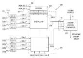
- FIG. 2illustrates a conventional column segmentation circuit for a memory device
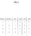
- FIG. 3is a table illustrating the input and output states of a decoder of the FIG. 2 circuit
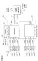
- FIG. 4is an exemplary multiplexer used in the FIG. 2 circuit
- FIG. 5is a chart illustrating column segmentation of a memory array based upon the conventional segmentation circuit of FIG. 2;
- FIG. 6illustrates a programmable column segmentation circuit in accordance with an exemplary embodiment of the present invention
- FIG. 7is table illustrating the input and output states of the segmentation decoder depicted in the FIG. 6 circuit
- FIG. 8is a chart illustrating one of the column segmentation arrangements which can be obtained by the FIG. 6 circuit
- FIG. 9illustrates a processor system employing a memory device containing the programmable column segmentation circuit of the invention.
- FIG. 1illustrates a simplified row address table for a memory device. Only sixteen rows (word lines) are shown here for simplicity of explanation. In practice, an actual DRAM would have many more rows and the address table would be correspondingly larger. Each of the rows ( 0 . . . 15 ) has four address bits identified as RowAdd 0 , RowAdd 1 , RowAdd 2 and RowAdd 3 which uniquely identify a row.
- the column segmentation device 200includes two input lines 250 , 252 connected as inputs to a segmentation decoder 204 . These input lines 250 , 252 respectively receive RowAdd 2 and RowAdd 3 bits from a presented row address signal.
- the RowAdd 2 and RowAdd 3 logic levelscan be used to identify four separate groups of rows, that is, four column segments.
- rows 15 - 12are identified as column segment 3 by the bit pattern “11”
- rows 11 - 8are identified as column segment 2 by the bit pattern “10”
- rows 7 - 4are identified as column segment 1 by the bit pattern “01”
- rows 3 - 0are identified as the column segment 0 by the bit pattern “00.”
- Each of the above segmentscontains four adjacent rows.
- Decoder 204provides a decoded output on lines 260 a, 260 b, 260 c, and 260 d in response to the RowAdd 2 and Row Add 3 bits, which corresponds to one of the four segments (row groups) in a column.
- Decoder 204is a very simple circuit containing signal inverters. It receives the RowAdd 2 and RowAdd 1 bits and respectively provides as an output signal on lines 260 a, 260 b, 260 c and 260 d the bits RowAdd 3 , ⁇ overscore (RowAdd 3 ) ⁇ , RowAdd 2 , and ⁇ overscore (RowAdd 2 ) ⁇ .
- FIG. 3is a table which shows the four possible combinations of inputs signals RowAdd 2 and RowAdd 3 and the corresponding decoded output on lines 260 a, 260 b, 260 c, and 260 d. Each unique combination of RowAdd 2 and RowAdd 3 logic bits (“11,” “10,” “01,” “00”) yields a unique decoded output.
- Each unique decoded outputindicates one of four column segments to a switching circuit 205 formed by a plurality of multiplexer circuits 206 a . . . 206 p .
- Each multiplexer 206receives the segment selection signals at the output of decoder 204 as control signals to select one of the inputs on lines 208 a′. . . a ′′′′ . . . 208 p ′ . . .
- each of the four latches for each multiplexer 206contains a programmed column bit value for a respective one of the column segments 3 , 2 , 1 , 0 .
- a defective bit in a column segment of a primary arrayis indicated by identifying the column address associated with the segment containing a defective bit.
- the indication of defective bitsis programmed by the fuses or antifuses 201 , and the programmed state of each fuse or antifuse is set into a corresponding latch 220 .
- a particular column segment3 , 2 , 1 , 0
- a latch corresponding to that segmentis selected by each multiplexer 206 for each of the sixteen bits of a column address to thereby indicate a defective column address.
- the collective sixteen bit output of the multiplexers 206 on respective output lines 256are applied to a column address comparator 217 , and when a column address is presented for a memory operation which matches the address for the defective column from the multiplexers 206 , a redundant column is selected in place of the primary column corresponding to the indicated defective column address.
- FIG. 4provides a detailed illustration of an exemplary multiplexer 206 .
- the column multiplexer 206is presented with the decoded output RowAdd 3 , ⁇ overscore (RowAdd) ⁇ 3 , ⁇ overscore (RowAdd) ⁇ 2 , RowAdd 2 on lines 260 a, 260 b, 260 c, and 260 d, only one of the four banks of transistors 280 , 282 , 284 , 286 are placed in a conductive state, thus allowing the defective primary column from the selected segment to pass through the multiplexers 206 .
- the exemplary column multiplexer 206may be any type of switching logic which yields the same results based upon the decoded output received from the decoder 204 .
- row 15is selected for a memory operation, and further assume column 3 of row 15 contains a defective cell and the column address for this defective cell is programmed in the latches 220 .
- the column 15 row address represented by “1 1 1 1”is presented to a memory device.
- the input line 252receives a high signal, “1” , (RowAdd 3 ) and input line 250 receives a high signal, “1” (RowAdd 2 ), and a column segment 3 containing row 15 is identified.
- the decoder 204decodes these inputs to produce a 4-bit signal (“1 0 1 0”) on lines 260 a, 260 b, 260 c, 260 d (see FIG. 2) which controls the multiplexers 206 a . . . 206 p to pass a defective column address bit pattern for column 3 precisely set into the latches 220 for segment 3 .
- the sixteen-bit address for column 3is presented to comparator 217 , it matches the address for defective column 3 passed by the multiplexers 206 and a redundant column is selected.
- the memory devicemay not have a sufficient number of available cells in the redundant column segments assigned to the primary columns to repair out all defective cells in columns of the primary memory array.
- the present inventionprovides for programmable selection of a segmentation arrangement for columns of the primary memory array based upon the row address of the defective cell.
- FIG. 6illustrates an exemplary embodiment of the invention. It differs from FIG. 2 in that the decoder 204 receives the RowAdd 2 bit on input line 250 , as in FIG. 2, but now decoder 204 receives either the RowAdd 3 bit, as in the FIG. 2 arrangement on line 442 , or a RowAdd 1 bit on line 440 on input line 252 , depending on the programmed condition of a switch 402 , e.g., a multiplexer, controlled by programmable line 444 which is connected to a programmable element 470 which may be either a fuse or antifuse.
- a switch 402e.g., a multiplexer
- programmable line 444which is connected to a programmable element 470 which may be either a fuse or antifuse.
- decoder 204receives the RowAdd 2 and RowAdd 3 input signals, as in FIG. 2, and operates as described above with reference to FIG. 2, while in the other state of programming of element 444 , the decoder
- FIG. 7indicates the output of decoder 204 for each of the possible states of the RowAdd 2 and RowAdd signals, which is the same truth table associated with decoder 204 of the FIG. 2 circuit; however, FIG. 8 shows how the column segments are now realigned.
- the RowAdd 2 and RowAdd 3 signalsare used, the four-column segments are arranged such that rows 12 through 15 are in column segment 3 , rows 8 through 11 are in column segment 2 , rows 4 through 7 are in column segment 1 and rows 3 through 0 are in column segment 0 , as shown in FIG. 5.
- RowAdd 2 and RowAdd 1 signalsare used as inputs to decoder 204 , the column segmentation is changed to the pattern shown in FIG. 8 where rows 6 , 7 , 14 , 15 are in column segment 3 , rows 4 , 5 , 12 , 13 are in column segment 2 , rows 2 , 3 , 10 , 11 are in column segment 1 and rows 0 , 1 , 8 , 9 are in column segment 0 .
- FIG. 6 circuitagain uses the decoder 204 output to select the appropriate one of the latches 220 for each multiplexer 206 to provide at the collective outputs 256 of the multiplexers 206 a programmed address of a defective column associated with each of the column segments. This address is sent to comparator 217 where it is compared to a presented column address and, if a match is found, a redundant column is selected.
- the column segmentation selection input line 444can be programmed by a programmable element 470 .
- Vcci.e., a high signal
- a low signalis passed to the column segmentation selection input line 444 if the antifuse is not blown. This is often referred to as “programming” the antifuse into one of two states.
- a fusemay also be used which is programmed into one of two logic states.
- programming of the circuit 400may be performed after the primary columns have been analyzed for cell failures and after various column segmentation arrangements have been tested for the optimum efficiency and for the segmentation arrangement which best fits the pattern of the cell defects. The more suitable segmentation arrangement is then selected by the programming of element 470 .
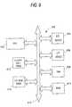
- FIG. 9illustrates a simplified processor system 600 which may use memory devices employing the invention as described and illustrated with reference to FIG. 4 and 5 .
- Processor system 600includes central processing unit (CPU) 612 , RAM and ROM memory devices 608 , 610 , input/output (I/O) devices 604 , 606 , floppy disk drive 614 and CD ROM drive 616 . All of the above components communicate with each other over one or more buses and/or bridges 618 .
- the RAM memory device 608may be formed as one or more memory modules, each of which contains one or more memory devices which may use the invention as described and illustrated with reference to FIG. 6, to provide for more efficient repair of defective primary columns of memory cells.
Landscapes
- For Increasing The Reliability Of Semiconductor Memories (AREA)
Abstract
Description
- I. Field of the Invention[0001]
- The present invention relates to a method and apparatus for implementing memory repair using column segmentation.[0002]
- II. Description of the Related Art[0003]
- In order to ensure proper operation, semiconductor devices are typically tested before being packaged into a chip. A series of probes at a test station electrically contact pads on each die to access portions of the individual semiconductor devices on the die. For example, in a semiconductor memory device, the probes contact address pads and data input/output pads to access selected memory cells in the memory device. Typical dynamic random access memory (“DRAM”) devices include one or more arrays of memory cells arranged in columns and rows. Each array of memory cells includes rows (word lines) that select memory cells along a selected row, and columns (bit lines or pairs of lines) that select memory cells along a column to read data from, or write data to, the selected memory cells in an memory array.[0004]
- During a pretest, predetermined data is typically written to selected column and row addresses that correspond to certain memory cells, and then the data is read from those memory cells to determine if the read data matches the data written to those addresses. If the read data does not match the written data, then the memory cells at the selected addresses likely contain defects and the semiconductor device fails the test.[0005]
- Many semiconductor memory devices include redundant columns of memory cells that can be employed to compensate for certain columns containing defective cells. As a result, by enabling such redundant circuitry, a tested memory device need not be discarded even if it fails a particular pretest. Thus, if a memory cell in a column of the primary memory array is defective, then an entire column of redundant memory cells can be substituted for the column of memory cells containing the defective cell.[0006]
- For memory devices employing redundant columns, column segmentation is often used. Column segmentation involves partitioning each column of the primary and redundant memory arrays. Therefore, if a portion of a primary column is found to be defective, only that portion of the primary column need be replaced and by only a portion of a redundant column. This preserves redundant column space, as only a limited number of redundant columns need to be fabricated on a memory device. Therefore, a memory device with more defective primary columns than redundant columns need not be scrapped as long as the defective segments of the primary columns can be substituted by an available segment of a redundant column.[0007]
- Traditional column segmentation is set uniformly across all primary and redundant columns. Thus, traditionally column segmentation provides several segments, where all of the rows of each particular column segment are arranged adjacent to one another and remain fixed in that arrangement. The arrangement is common across all primary and redundant columns. With this traditional fixed segmentation scheme it is possible, depending on the location of defective cells, to have fewer available redundant segments for repair than primary segments which need repair. In this case, the memory device would be unrepairable because some defective segments of the primary array do not have a substitute redundant segment available for repair. A more flexible and efficient column segmentation arrangement would be desirable.[0008]
- The present invention provides a method and apparatus which provides more efficient and flexible column segmentation in a memory device utilizing redundant columns. The present invention provides for a programmable column segmentation arrangement in which the particular rows associated with a column segment can be changed permitting more flexibility in primary column repair.[0009]
- Thus, after the primary columns have been analyzed for cell failures and after various column segmentation arrangements have been tested for optimum efficiency, a column segmentation arrangement can be selected to best suit the cell failures of the memory device.[0010]
- The foregoing and other advantages and features of the invention will become more apparent from the detailed description of exemplary embodiments provided below with reference to the accompanying drawings in which:[0011]
- FIG. 1 shows a representative row address table for a memory device;[0012]
- FIG. 2 illustrates a conventional column segmentation circuit for a memory device;[0013]
- FIG. 3 is a table illustrating the input and output states of a decoder of the FIG. 2 circuit;[0014]
- FIG. 4 is an exemplary multiplexer used in the FIG. 2 circuit;[0015]
- FIG. 5 is a chart illustrating column segmentation of a memory array based upon the conventional segmentation circuit of FIG. 2;[0016]
- FIG. 6 illustrates a programmable column segmentation circuit in accordance with an exemplary embodiment of the present invention;[0017]
- FIG. 7 is table illustrating the input and output states of the segmentation decoder depicted in the FIG. 6 circuit;[0018]
- FIG. 8 is a chart illustrating one of the column segmentation arrangements which can be obtained by the FIG. 6 circuit;[0019]
- FIG. 9 illustrates a processor system employing a memory device containing the programmable column segmentation circuit of the invention.[0020]
- Before describing the invention, a conventional[0021]
column segmentation device 200 which is used in memory devices and depicted in FIG. 2, will be described in connection with the row address table shown in the FIG. 1. - FIG. 1 illustrates a simplified row address table for a memory device. Only sixteen rows (word lines) are shown here for simplicity of explanation. In practice, an actual DRAM would have many more rows and the address table would be correspondingly larger. Each of the rows ([0022]0 . . .15) has four address bits identified as RowAdd0, RowAdd1, RowAdd2 and RowAdd3 which uniquely identify a row.
- Referring to FIG. 2, the[0023]
column segmentation device 200 includes twoinput lines segmentation decoder 204. Theseinput lines RowAdd 2 andRowAdd 3 bits from a presented row address signal. - As shown in FIG. 5, the RowAdd[0024]2 and RowAdd3 logic levels can be used to identify four separate groups of rows, that is, four column segments. For example, as shown in FIG. 5, rows15-12 are identified as
column segment 3 by the bit pattern “11,” rows11-8 are identified ascolumn segment 2 by the bit pattern “10,” rows7-4 are identified ascolumn segment 1 by the bit pattern “01,” and rows3-0 are identified as thecolumn segment 0 by the bit pattern “00.” Each of the above segments contains four adjacent rows.Decoder 204 provides a decoded output on lines260a,260b,260c,and260din response to the RowAdd2 and Row Add3 bits, which corresponds to one of the four segments (row groups) in a column. - [0025]
Decoder 204 is a very simple circuit containing signal inverters. It receives theRowAdd 2 and RowAdd1 bits and respectively provides as an output signal on lines260a,260b,260cand260dthe bits RowAdd3, {overscore (RowAdd3)}, RowAdd2, and {overscore (RowAdd2)}. FIG.3 is a table which shows the four possible combinations of inputs signals RowAdd2 and RowAdd3 and the corresponding decoded output on lines260a,260b,260c,and260d.Each unique combination of RowAdd2 and RowAdd3 logic bits (“11,” “10,” “01,” “00”) yields a unique decoded output. Each unique decoded output indicates one of four column segments to aswitching circuit 205 formed by a plurality of multiplexer circuits206a. . .206p. In the illustrated circuit there is one multiplexer circuit206a. . .206pfor each bit position of a column address of a memory device. Assuming use of a sixteen-bit column address, there will be sixteen multiplexers206a. . .206p. Eachmultiplexer 206 receives the segment selection signals at the output ofdecoder 204 as control signals to select one of the inputs on lines208a′. . . a″″ . . .208p′ . . .208p″″ and pass it to arespective output line 256. The input lines208a′ . . .208a″″ . . .208p′ . . . p″″ are respectively coupled to latchcircuits 220a′ . . . a″″ . . .220p′ . . . p″″ respectively associated with aprogrammable element 201 such as a fuse or antifuse, only one of which is shown in FIG. 2. The fuses/antifuses 201 are used to program into thelatches 220 the addresses of the defective columns for each of the four column segments. Thus, as shown in FIG. 2, each of the four latches for each multiplexer206 contains a programmed column bit value for a respective one of thecolumn segments - A defective bit in a column segment of a primary array is indicated by identifying the column address associated with the segment containing a defective bit. The indication of defective bits is programmed by the fuses or[0026]
antifuses 201, and the programmed state of each fuse or antifuse is set into acorresponding latch 220. Thus, if a particular column segment (3,2,1,0) contains a defective bit, when the segment, e.g.,3, is indicated by the output of thedecoder 204, a latch corresponding to that segment is selected by eachmultiplexer 206 for each of the sixteen bits of a column address to thereby indicate a defective column address. - The collective sixteen bit output of the[0027]
multiplexers 206 onrespective output lines 256 are applied to acolumn address comparator 217, and when a column address is presented for a memory operation which matches the address for the defective column from themultiplexers 206, a redundant column is selected in place of the primary column corresponding to the indicated defective column address. - FIG. 4 provides a detailed illustration of an[0028]
exemplary multiplexer 206. As can be seen, when thecolumn multiplexer 206 is presented with the decodedoutput RowAdd 3, {overscore (RowAdd)}3, {overscore (RowAdd)}2,RowAdd 2 on lines260a,260b,260c,and260d,only one of the four banks oftransistors multiplexers 206. Theexemplary column multiplexer 206 may be any type of switching logic which yields the same results based upon the decoded output received from thedecoder 204. - As an example of the operation of the FIG. 2 circuit, assume[0029]
row 15 is selected for a memory operation, and further assumecolumn 3 ofrow 15 contains a defective cell and the column address for this defective cell is programmed in thelatches 220. Thecolumn 15 row address represented by “1 1 1 1” is presented to a memory device. In this case, theinput line 252 receives a high signal, “1” , (RowAdd3) andinput line 250 receives a high signal, “1” (RowAdd2), and acolumn segment 3 containingrow 15 is identified. Thedecoder 204 decodes these inputs to produce a 4-bit signal (“1 0 1 0”) on lines260a,260b,260c,260d(see FIG. 2) which controls the multiplexers206a. . .206pto pass a defective column address bit pattern forcolumn 3 precisely set into thelatches 220 forsegment 3. When the sixteen-bit address forcolumn 3 is presented tocomparator 217, it matches the address fordefective column 3 passed by themultiplexers 206 and a redundant column is selected. - Depending on where defective cells are located in the primary array, the memory device may not have a sufficient number of available cells in the redundant column segments assigned to the primary columns to repair out all defective cells in columns of the primary memory array.[0030]
- In order to reduce the number of unrepairable memory devices, the present invention provides for programmable selection of a segmentation arrangement for columns of the primary memory array based upon the row address of the defective cell.[0031]
- FIG. 6 illustrates an exemplary embodiment of the invention. It differs from FIG. 2 in that the[0032]
decoder 204 receives the RowAdd2 bit oninput line 250, as in FIG. 2, but now decoder204 receives either theRowAdd 3 bit, as in the FIG. 2 arrangement online 442, or a RowAdd1 bit online 440 oninput line 252, depending on the programmed condition of a switch402, e.g., a multiplexer, controlled byprogrammable line 444 which is connected to aprogrammable element 470 which may be either a fuse or antifuse. Thus, in one state of programming ofelement 470,decoder 204 receives the RowAdd2 and RowAdd3 input signals, as in FIG. 2, and operates as described above with reference to FIG. 2, while in the other state of programming ofelement 444, thedecoder 204 receives the RowAdd2 and RowAdd1 bits as input signals, and the FIG. 6 circuit operates differently from the FIG. 2 circuit. - When the RowAdd[0033]2 and RowAdd1 bits are used as inputs to
decoder 204, the column segmentation is different from that of the FIG. 2 circuit. FIG. 7 indicates the output ofdecoder 204 for each of the possible states of the RowAdd2 and RowAdd signals, which is the same truth table associated withdecoder 204 of the FIG. 2 circuit; however, FIG. 8 shows how the column segments are now realigned. Referring back to FIG. 5, when the RowAdd2 and RowAdd3 signals are used, the four-column segments are arranged such thatrows 12 through15 are incolumn segment 3,rows 8 through11 are incolumn segment 2,rows 4 through7 are incolumn segment 1 androws 3 through0 are incolumn segment 0, as shown in FIG. 5. However, when the RowAdd2 and RowAdd1 signals are used as inputs todecoder 204, the column segmentation is changed to the pattern shown in FIG. 8 whererows column segment 3,rows column segment 2,rows column segment 1 androws column segment 0. - The FIG. 6 circuit again uses the[0034]
decoder 204 output to select the appropriate one of thelatches 220 for each multiplexer206 to provide at thecollective outputs 256 of the multiplexers206 a programmed address of a defective column associated with each of the column segments. This address is sent tocomparator 217 where it is compared to a presented column address and, if a match is found, a redundant column is selected. - Thus, after a memory test is performed and defective cells are identified, two different column segmentation patterns are available which can be used to map redundant column segments to primary column segments. This provides a greater degree of flexibility in repairing out defective column segments.[0035]
- As noted, in order to maximize flexibility of repair out of defective cells, the column segmentation[0036]
selection input line 444 can be programmed by aprogrammable element 470. In the case of an antifuse asprogrammable element 470, Vcc (i.e., a high signal) is passed to the columnsegmentation selection input 444 if the antifuse is blown. A low signal is passed to the column segmentationselection input line 444 if the antifuse is not blown. This is often referred to as “programming” the antifuse into one of two states. (Alternatively, a fuse may also be used which is programmed into one of two logic states.) In this way programming of thecircuit 400 may be performed after the primary columns have been analyzed for cell failures and after various column segmentation arrangements have been tested for the optimum efficiency and for the segmentation arrangement which best fits the pattern of the cell defects. The more suitable segmentation arrangement is then selected by the programming ofelement 470. - It should be noted that the invention could also be used to segment word lines of a memory instead of column lines if repairs are based on the use of redundant rows instead of redundant columns.[0037]
- FIG. 9 illustrates a simplified processor system[0038]600 which may use memory devices employing the invention as described and illustrated with reference to FIG. 4 and5. Processor system600 includes central processing unit (CPU)612, RAM and
ROM memory devices devices floppy disk drive 614 andCD ROM drive 616. All of the above components communicate with each other over one or more buses and/or bridges618. TheRAM memory device 608 may be formed as one or more memory modules, each of which contains one or more memory devices which may use the invention as described and illustrated with reference to FIG. 6, to provide for more efficient repair of defective primary columns of memory cells. - While an exemplary embodiment of invention have been described and illustrated, it is to be understood that the above description is intended to be illustrative and not restrictive. Many variations to the above-described circuit and method will be readily apparent to those having ordinary skill in the art.[0039]
- Accordingly, the present invention is not to be considered as limited by the specifics of the particular circuit and method which have been described and illustrated, but is only limited by the scope of the appended claims.[0040]
Claims (37)
Priority Applications (2)
| Application Number | Priority Date | Filing Date | Title |
|---|---|---|---|
| US09/818,617US6552937B2 (en) | 2001-03-28 | 2001-03-28 | Memory device having programmable column segmentation to increase flexibility in bit repair |
| US10/367,933US6788597B2 (en) | 2001-03-28 | 2003-02-19 | Memory device having programmable column segmentation to increase flexibility in bit repair |
Applications Claiming Priority (1)
| Application Number | Priority Date | Filing Date | Title |
|---|---|---|---|
| US09/818,617US6552937B2 (en) | 2001-03-28 | 2001-03-28 | Memory device having programmable column segmentation to increase flexibility in bit repair |
Related Child Applications (1)
| Application Number | Title | Priority Date | Filing Date |
|---|---|---|---|
| US10/367,933DivisionUS6788597B2 (en) | 2001-03-28 | 2003-02-19 | Memory device having programmable column segmentation to increase flexibility in bit repair |
Publications (2)
| Publication Number | Publication Date |
|---|---|
| US20020141254A1true US20020141254A1 (en) | 2002-10-03 |
| US6552937B2 US6552937B2 (en) | 2003-04-22 |
Family
ID=25225965
Family Applications (2)
| Application Number | Title | Priority Date | Filing Date |
|---|---|---|---|
| US09/818,617Expired - LifetimeUS6552937B2 (en) | 2001-03-28 | 2001-03-28 | Memory device having programmable column segmentation to increase flexibility in bit repair |
| US10/367,933Expired - LifetimeUS6788597B2 (en) | 2001-03-28 | 2003-02-19 | Memory device having programmable column segmentation to increase flexibility in bit repair |
Family Applications After (1)
| Application Number | Title | Priority Date | Filing Date |
|---|---|---|---|
| US10/367,933Expired - LifetimeUS6788597B2 (en) | 2001-03-28 | 2003-02-19 | Memory device having programmable column segmentation to increase flexibility in bit repair |
Country Status (1)
| Country | Link |
|---|---|
| US (2) | US6552937B2 (en) |
Cited By (2)
| Publication number | Priority date | Publication date | Assignee | Title |
|---|---|---|---|---|
| US20040153725A1 (en)* | 2003-02-04 | 2004-08-05 | Micron Technology, Inc. | ROM redundancy in ROM embedded DRAM |
| US20140219023A1 (en)* | 2009-07-06 | 2014-08-07 | Sandisk Technologies Inc. | Bad Column Management with Bit Information in Non-Volatile Memory Systems |
Families Citing this family (12)
| Publication number | Priority date | Publication date | Assignee | Title |
|---|---|---|---|---|
| US6552937B2 (en)* | 2001-03-28 | 2003-04-22 | Micron Technology, Inc. | Memory device having programmable column segmentation to increase flexibility in bit repair |
| US7003643B1 (en) | 2001-04-16 | 2006-02-21 | Micron Technology, Inc. | Burst counter controller and method in a memory device operable in a 2-bit prefetch mode |
| US7003653B2 (en)* | 2002-10-21 | 2006-02-21 | Sun Microsystems, Inc. | Method for rapid interpretation of results returned by a parallel compare instruction |
| US6831868B2 (en)* | 2002-12-05 | 2004-12-14 | Intel Corporation | Byte aligned redundancy for memory array |
| US6807114B2 (en)* | 2003-01-17 | 2004-10-19 | Micron Technology, Inc. | Method and system for selecting redundant rows and columns of memory cells |
| US7509543B2 (en)* | 2003-06-17 | 2009-03-24 | Micron Technology, Inc. | Circuit and method for error test, recordation, and repair |
| US6868019B2 (en)* | 2003-07-02 | 2005-03-15 | Micron Technology, Inc. | Reduced power redundancy address decoder and comparison circuit |
| KR100551485B1 (en)* | 2003-12-04 | 2006-02-13 | 삼성전자주식회사 | Timing Control Method of Memory Device |
| JP4102338B2 (en)* | 2004-07-20 | 2008-06-18 | 株式会社東芝 | Semiconductor memory device |
| US6944075B1 (en) | 2005-01-05 | 2005-09-13 | International Business Machines Corporation | Variable column redundancy region boundaries in SRAM |
| US7379360B1 (en)* | 2006-10-31 | 2008-05-27 | Hynix Semiconductor Inc. | Repair fuse circuit for storing I/O repair information therein |
| US11037653B2 (en) | 2018-10-05 | 2021-06-15 | Samsung Electronics Co., Ltd. | Memory devices performing repair operations and repair operation methods thereof |
Family Cites Families (13)
| Publication number | Priority date | Publication date | Assignee | Title |
|---|---|---|---|---|
| US5309446A (en)* | 1990-07-31 | 1994-05-03 | Texas Instruments Incorporated | Test validation method for a semiconductor memory device |
| ATE200939T1 (en)* | 1993-02-19 | 2001-05-15 | Infineon Technologies Ag | COLUMN REDUNDANCY CIRCUIT ARRANGEMENT FOR A MEMORY |
| US5822256A (en)* | 1994-09-06 | 1998-10-13 | Intel Corporation | Method and circuitry for usage of partially functional nonvolatile memory |
| US5901105A (en)* | 1995-04-05 | 1999-05-04 | Ong; Adrian E | Dynamic random access memory having decoding circuitry for partial memory blocks |
| US5619460A (en)* | 1995-06-07 | 1997-04-08 | International Business Machines Corporation | Method of testing a random access memory |
| US5912812A (en)* | 1996-12-19 | 1999-06-15 | Lucent Technologies Inc. | Boost power converter for powering a load from an AC source |
| US5923129A (en)* | 1997-03-14 | 1999-07-13 | Linfinity Microelectronics | Apparatus and method for starting a fluorescent lamp |
| US5930121A (en)* | 1997-03-14 | 1999-07-27 | Linfinity Microelectronics | Direct drive backlight system |
| US6198234B1 (en)* | 1999-06-09 | 2001-03-06 | Linfinity Microelectronics | Dimmable backlight system |
| US6163489A (en)* | 1999-07-16 | 2000-12-19 | Micron Technology Inc. | Semiconductor memory having multiple redundant columns with offset segmentation boundaries |
| US6418068B1 (en)* | 2001-01-19 | 2002-07-09 | Hewlett-Packard Co. | Self-healing memory |
| US6373758B1 (en)* | 2001-02-23 | 2002-04-16 | Hewlett-Packard Company | System and method of operating a programmable column fail counter for redundancy allocation |
| US6552937B2 (en)* | 2001-03-28 | 2003-04-22 | Micron Technology, Inc. | Memory device having programmable column segmentation to increase flexibility in bit repair |
- 2001
- 2001-03-28USUS09/818,617patent/US6552937B2/ennot_activeExpired - Lifetime
- 2003
- 2003-02-19USUS10/367,933patent/US6788597B2/ennot_activeExpired - Lifetime
Cited By (6)
| Publication number | Priority date | Publication date | Assignee | Title |
|---|---|---|---|---|
| US20040153725A1 (en)* | 2003-02-04 | 2004-08-05 | Micron Technology, Inc. | ROM redundancy in ROM embedded DRAM |
| US7174477B2 (en)* | 2003-02-04 | 2007-02-06 | Micron Technology, Inc. | ROM redundancy in ROM embedded DRAM |
| US20070168783A1 (en)* | 2003-02-04 | 2007-07-19 | Micron Technology, Inc. | ROM redundancy in ROM embedded DRAM |
| US7366946B2 (en)* | 2003-02-04 | 2008-04-29 | Micron Technology, Inc. | ROM redundancy in ROM embedded DRAM |
| US20140219023A1 (en)* | 2009-07-06 | 2014-08-07 | Sandisk Technologies Inc. | Bad Column Management with Bit Information in Non-Volatile Memory Systems |
| US9748001B2 (en)* | 2009-07-06 | 2017-08-29 | Sandisk Technologies Llc | Bad column management with bit information in non-volatile memory systems |
Also Published As
| Publication number | Publication date |
|---|---|
| US6552937B2 (en) | 2003-04-22 |
| US6788597B2 (en) | 2004-09-07 |
| US20030147292A1 (en) | 2003-08-07 |
Similar Documents
| Publication | Publication Date | Title |
|---|---|---|
| US6940765B2 (en) | Repair apparatus and method for semiconductor memory device to be selectively programmed for wafer-level test or post package test | |
| US6128756A (en) | System for optimizing the testing and repair time of a defective integrated circuit | |
| US5153880A (en) | Field-programmable redundancy apparatus for memory arrays | |
| US5961653A (en) | Processor based BIST for an embedded memory | |
| KR102117633B1 (en) | Self repair device | |
| US5161157A (en) | Field-programmable redundancy apparatus for memory arrays | |
| US6968482B2 (en) | Memory redundancy with programmable non-volatile control | |
| US6434067B1 (en) | Semiconductor memory having multiple redundant columns with offset segmentation boundaries | |
| EP0049629A2 (en) | Redundancy scheme for a dynamic RAM | |
| US20060203580A1 (en) | Programmable element latch circuit | |
| JP2588692B2 (en) | Redundant register programming method and column redundant integrated circuit | |
| US6552937B2 (en) | Memory device having programmable column segmentation to increase flexibility in bit repair | |
| GB2129585A (en) | Memory system including a faulty rom array | |
| US6208570B1 (en) | Redundancy test method for a semiconductor memory | |
| US20060197178A1 (en) | Electrical fuses with redundancy | |
| US5561636A (en) | Random access memory with a simple test arrangement | |
| EP0070823A1 (en) | Semiconductor memory redundant element identification circuit | |
| US6535436B2 (en) | Redundant circuit and method for replacing defective memory cells in a memory device | |
| US5708601A (en) | Integrated circuitry for checking the utilization rate of redundancy memory elements in a semiconductor memory device | |
| US7055075B2 (en) | Apparatus for random access memory array self-test | |
| US7218561B2 (en) | Apparatus and method for semiconductor device repair with reduced number of programmable elements | |
| US6243305B1 (en) | Memory redundancy device and method | |
| JPH06203594A (en) | Semiconductor memory device | |
| JP2001312897A (en) | Memory test device and test method | |
| US6345013B1 (en) | Latched row or column select enable driver |
Legal Events
| Date | Code | Title | Description |
|---|---|---|---|
| AS | Assignment | Owner name:MICRON TECHNOLOGY, INC., IDAHO Free format text:ASSIGNMENT OF ASSIGNORS INTEREST;ASSIGNORS:LADNER, BRIAN J.;PENNEY, DANIEL B.;REEL/FRAME:011646/0540 Effective date:20010326 | |
| STCF | Information on status: patent grant | Free format text:PATENTED CASE | |
| FPAY | Fee payment | Year of fee payment:4 | |
| FEPP | Fee payment procedure | Free format text:PAYER NUMBER DE-ASSIGNED (ORIGINAL EVENT CODE: RMPN); ENTITY STATUS OF PATENT OWNER: LARGE ENTITY Free format text:PAYOR NUMBER ASSIGNED (ORIGINAL EVENT CODE: ASPN); ENTITY STATUS OF PATENT OWNER: LARGE ENTITY | |
| FPAY | Fee payment | Year of fee payment:8 | |
| FPAY | Fee payment | Year of fee payment:12 | |
| AS | Assignment | Owner name:U.S. BANK NATIONAL ASSOCIATION, AS COLLATERAL AGENT, CALIFORNIA Free format text:SECURITY INTEREST;ASSIGNOR:MICRON TECHNOLOGY, INC.;REEL/FRAME:038669/0001 Effective date:20160426 Owner name:U.S. BANK NATIONAL ASSOCIATION, AS COLLATERAL AGEN Free format text:SECURITY INTEREST;ASSIGNOR:MICRON TECHNOLOGY, INC.;REEL/FRAME:038669/0001 Effective date:20160426 | |
| AS | Assignment | Owner name:MORGAN STANLEY SENIOR FUNDING, INC., AS COLLATERAL AGENT, MARYLAND Free format text:PATENT SECURITY AGREEMENT;ASSIGNOR:MICRON TECHNOLOGY, INC.;REEL/FRAME:038954/0001 Effective date:20160426 Owner name:MORGAN STANLEY SENIOR FUNDING, INC., AS COLLATERAL Free format text:PATENT SECURITY AGREEMENT;ASSIGNOR:MICRON TECHNOLOGY, INC.;REEL/FRAME:038954/0001 Effective date:20160426 | |
| AS | Assignment | Owner name:U.S. BANK NATIONAL ASSOCIATION, AS COLLATERAL AGENT, CALIFORNIA Free format text:CORRECTIVE ASSIGNMENT TO CORRECT THE REPLACE ERRONEOUSLY FILED PATENT #7358718 WITH THE CORRECT PATENT #7358178 PREVIOUSLY RECORDED ON REEL 038669 FRAME 0001. ASSIGNOR(S) HEREBY CONFIRMS THE SECURITY INTEREST;ASSIGNOR:MICRON TECHNOLOGY, INC.;REEL/FRAME:043079/0001 Effective date:20160426 Owner name:U.S. BANK NATIONAL ASSOCIATION, AS COLLATERAL AGEN Free format text:CORRECTIVE ASSIGNMENT TO CORRECT THE REPLACE ERRONEOUSLY FILED PATENT #7358718 WITH THE CORRECT PATENT #7358178 PREVIOUSLY RECORDED ON REEL 038669 FRAME 0001. ASSIGNOR(S) HEREBY CONFIRMS THE SECURITY INTEREST;ASSIGNOR:MICRON TECHNOLOGY, INC.;REEL/FRAME:043079/0001 Effective date:20160426 | |
| AS | Assignment | Owner name:JPMORGAN CHASE BANK, N.A., AS COLLATERAL AGENT, ILLINOIS Free format text:SECURITY INTEREST;ASSIGNORS:MICRON TECHNOLOGY, INC.;MICRON SEMICONDUCTOR PRODUCTS, INC.;REEL/FRAME:047540/0001 Effective date:20180703 Owner name:JPMORGAN CHASE BANK, N.A., AS COLLATERAL AGENT, IL Free format text:SECURITY INTEREST;ASSIGNORS:MICRON TECHNOLOGY, INC.;MICRON SEMICONDUCTOR PRODUCTS, INC.;REEL/FRAME:047540/0001 Effective date:20180703 | |
| AS | Assignment | Owner name:MICRON TECHNOLOGY, INC., IDAHO Free format text:RELEASE BY SECURED PARTY;ASSIGNOR:U.S. BANK NATIONAL ASSOCIATION, AS COLLATERAL AGENT;REEL/FRAME:047243/0001 Effective date:20180629 | |
| AS | Assignment | Owner name:MICRON TECHNOLOGY, INC., IDAHO Free format text:RELEASE BY SECURED PARTY;ASSIGNOR:MORGAN STANLEY SENIOR FUNDING, INC., AS COLLATERAL AGENT;REEL/FRAME:050937/0001 Effective date:20190731 | |
| AS | Assignment | Owner name:MICRON TECHNOLOGY, INC., IDAHO Free format text:RELEASE BY SECURED PARTY;ASSIGNOR:JPMORGAN CHASE BANK, N.A., AS COLLATERAL AGENT;REEL/FRAME:051028/0001 Effective date:20190731 Owner name:MICRON SEMICONDUCTOR PRODUCTS, INC., IDAHO Free format text:RELEASE BY SECURED PARTY;ASSIGNOR:JPMORGAN CHASE BANK, N.A., AS COLLATERAL AGENT;REEL/FRAME:051028/0001 Effective date:20190731 |