US20020140646A1 - Display module - Google Patents
Display moduleDownload PDFInfo
- Publication number
- US20020140646A1 US20020140646A1US10/105,308US10530802AUS2002140646A1US 20020140646 A1US20020140646 A1US 20020140646A1US 10530802 AUS10530802 AUS 10530802AUS 2002140646 A1US2002140646 A1US 2002140646A1
- Authority
- US
- United States
- Prior art keywords
- electrode layer
- current supply
- terminal pad
- display module
- substrate
- Prior art date
- Legal status (The legal status is an assumption and is not a legal conclusion. Google has not performed a legal analysis and makes no representation as to the accuracy of the status listed.)
- Granted
Links
Images


Classifications
- G—PHYSICS
- G09—EDUCATION; CRYPTOGRAPHY; DISPLAY; ADVERTISING; SEALS
- G09F—DISPLAYING; ADVERTISING; SIGNS; LABELS OR NAME-PLATES; SEALS
- G09F9/00—Indicating arrangements for variable information in which the information is built-up on a support by selection or combination of individual elements
- G09F9/30—Indicating arrangements for variable information in which the information is built-up on a support by selection or combination of individual elements in which the desired character or characters are formed by combining individual elements
- G—PHYSICS
- G09—EDUCATION; CRYPTOGRAPHY; DISPLAY; ADVERTISING; SEALS
- G09G—ARRANGEMENTS OR CIRCUITS FOR CONTROL OF INDICATING DEVICES USING STATIC MEANS TO PRESENT VARIABLE INFORMATION
- G09G3/00—Control arrangements or circuits, of interest only in connection with visual indicators other than cathode-ray tubes
- G09G3/20—Control arrangements or circuits, of interest only in connection with visual indicators other than cathode-ray tubes for presentation of an assembly of a number of characters, e.g. a page, by composing the assembly by combination of individual elements arranged in a matrix no fixed position being assigned to or needed to be assigned to the individual characters or partial characters
- G09G3/22—Control arrangements or circuits, of interest only in connection with visual indicators other than cathode-ray tubes for presentation of an assembly of a number of characters, e.g. a page, by composing the assembly by combination of individual elements arranged in a matrix no fixed position being assigned to or needed to be assigned to the individual characters or partial characters using controlled light sources
- G09G3/30—Control arrangements or circuits, of interest only in connection with visual indicators other than cathode-ray tubes for presentation of an assembly of a number of characters, e.g. a page, by composing the assembly by combination of individual elements arranged in a matrix no fixed position being assigned to or needed to be assigned to the individual characters or partial characters using controlled light sources using electroluminescent panels
- G09G3/32—Control arrangements or circuits, of interest only in connection with visual indicators other than cathode-ray tubes for presentation of an assembly of a number of characters, e.g. a page, by composing the assembly by combination of individual elements arranged in a matrix no fixed position being assigned to or needed to be assigned to the individual characters or partial characters using controlled light sources using electroluminescent panels semiconductive, e.g. using light-emitting diodes [LED]
- G09G3/3208—Control arrangements or circuits, of interest only in connection with visual indicators other than cathode-ray tubes for presentation of an assembly of a number of characters, e.g. a page, by composing the assembly by combination of individual elements arranged in a matrix no fixed position being assigned to or needed to be assigned to the individual characters or partial characters using controlled light sources using electroluminescent panels semiconductive, e.g. using light-emitting diodes [LED] organic, e.g. using organic light-emitting diodes [OLED]
- G09G3/3225—Control arrangements or circuits, of interest only in connection with visual indicators other than cathode-ray tubes for presentation of an assembly of a number of characters, e.g. a page, by composing the assembly by combination of individual elements arranged in a matrix no fixed position being assigned to or needed to be assigned to the individual characters or partial characters using controlled light sources using electroluminescent panels semiconductive, e.g. using light-emitting diodes [LED] organic, e.g. using organic light-emitting diodes [OLED] using an active matrix
- G09G3/3233—Control arrangements or circuits, of interest only in connection with visual indicators other than cathode-ray tubes for presentation of an assembly of a number of characters, e.g. a page, by composing the assembly by combination of individual elements arranged in a matrix no fixed position being assigned to or needed to be assigned to the individual characters or partial characters using controlled light sources using electroluminescent panels semiconductive, e.g. using light-emitting diodes [LED] organic, e.g. using organic light-emitting diodes [OLED] using an active matrix with pixel circuitry controlling the current through the light-emitting element
- G—PHYSICS
- G09—EDUCATION; CRYPTOGRAPHY; DISPLAY; ADVERTISING; SEALS
- G09G—ARRANGEMENTS OR CIRCUITS FOR CONTROL OF INDICATING DEVICES USING STATIC MEANS TO PRESENT VARIABLE INFORMATION
- G09G3/00—Control arrangements or circuits, of interest only in connection with visual indicators other than cathode-ray tubes
- G09G3/20—Control arrangements or circuits, of interest only in connection with visual indicators other than cathode-ray tubes for presentation of an assembly of a number of characters, e.g. a page, by composing the assembly by combination of individual elements arranged in a matrix no fixed position being assigned to or needed to be assigned to the individual characters or partial characters
- G09G3/22—Control arrangements or circuits, of interest only in connection with visual indicators other than cathode-ray tubes for presentation of an assembly of a number of characters, e.g. a page, by composing the assembly by combination of individual elements arranged in a matrix no fixed position being assigned to or needed to be assigned to the individual characters or partial characters using controlled light sources
- G09G3/30—Control arrangements or circuits, of interest only in connection with visual indicators other than cathode-ray tubes for presentation of an assembly of a number of characters, e.g. a page, by composing the assembly by combination of individual elements arranged in a matrix no fixed position being assigned to or needed to be assigned to the individual characters or partial characters using controlled light sources using electroluminescent panels
- G09G3/32—Control arrangements or circuits, of interest only in connection with visual indicators other than cathode-ray tubes for presentation of an assembly of a number of characters, e.g. a page, by composing the assembly by combination of individual elements arranged in a matrix no fixed position being assigned to or needed to be assigned to the individual characters or partial characters using controlled light sources using electroluminescent panels semiconductive, e.g. using light-emitting diodes [LED]
- G09G3/3208—Control arrangements or circuits, of interest only in connection with visual indicators other than cathode-ray tubes for presentation of an assembly of a number of characters, e.g. a page, by composing the assembly by combination of individual elements arranged in a matrix no fixed position being assigned to or needed to be assigned to the individual characters or partial characters using controlled light sources using electroluminescent panels semiconductive, e.g. using light-emitting diodes [LED] organic, e.g. using organic light-emitting diodes [OLED]
- G09G3/3225—Control arrangements or circuits, of interest only in connection with visual indicators other than cathode-ray tubes for presentation of an assembly of a number of characters, e.g. a page, by composing the assembly by combination of individual elements arranged in a matrix no fixed position being assigned to or needed to be assigned to the individual characters or partial characters using controlled light sources using electroluminescent panels semiconductive, e.g. using light-emitting diodes [LED] organic, e.g. using organic light-emitting diodes [OLED] using an active matrix
- G—PHYSICS
- G09—EDUCATION; CRYPTOGRAPHY; DISPLAY; ADVERTISING; SEALS
- G09G—ARRANGEMENTS OR CIRCUITS FOR CONTROL OF INDICATING DEVICES USING STATIC MEANS TO PRESENT VARIABLE INFORMATION
- G09G3/00—Control arrangements or circuits, of interest only in connection with visual indicators other than cathode-ray tubes
- G09G3/20—Control arrangements or circuits, of interest only in connection with visual indicators other than cathode-ray tubes for presentation of an assembly of a number of characters, e.g. a page, by composing the assembly by combination of individual elements arranged in a matrix no fixed position being assigned to or needed to be assigned to the individual characters or partial characters
- G09G3/22—Control arrangements or circuits, of interest only in connection with visual indicators other than cathode-ray tubes for presentation of an assembly of a number of characters, e.g. a page, by composing the assembly by combination of individual elements arranged in a matrix no fixed position being assigned to or needed to be assigned to the individual characters or partial characters using controlled light sources
- G09G3/30—Control arrangements or circuits, of interest only in connection with visual indicators other than cathode-ray tubes for presentation of an assembly of a number of characters, e.g. a page, by composing the assembly by combination of individual elements arranged in a matrix no fixed position being assigned to or needed to be assigned to the individual characters or partial characters using controlled light sources using electroluminescent panels
- G09G3/32—Control arrangements or circuits, of interest only in connection with visual indicators other than cathode-ray tubes for presentation of an assembly of a number of characters, e.g. a page, by composing the assembly by combination of individual elements arranged in a matrix no fixed position being assigned to or needed to be assigned to the individual characters or partial characters using controlled light sources using electroluminescent panels semiconductive, e.g. using light-emitting diodes [LED]
- G09G3/3208—Control arrangements or circuits, of interest only in connection with visual indicators other than cathode-ray tubes for presentation of an assembly of a number of characters, e.g. a page, by composing the assembly by combination of individual elements arranged in a matrix no fixed position being assigned to or needed to be assigned to the individual characters or partial characters using controlled light sources using electroluminescent panels semiconductive, e.g. using light-emitting diodes [LED] organic, e.g. using organic light-emitting diodes [OLED]
- G09G3/3266—Details of drivers for scan electrodes
- G—PHYSICS
- G09—EDUCATION; CRYPTOGRAPHY; DISPLAY; ADVERTISING; SEALS
- G09G—ARRANGEMENTS OR CIRCUITS FOR CONTROL OF INDICATING DEVICES USING STATIC MEANS TO PRESENT VARIABLE INFORMATION
- G09G3/00—Control arrangements or circuits, of interest only in connection with visual indicators other than cathode-ray tubes
- G09G3/20—Control arrangements or circuits, of interest only in connection with visual indicators other than cathode-ray tubes for presentation of an assembly of a number of characters, e.g. a page, by composing the assembly by combination of individual elements arranged in a matrix no fixed position being assigned to or needed to be assigned to the individual characters or partial characters
- G09G3/22—Control arrangements or circuits, of interest only in connection with visual indicators other than cathode-ray tubes for presentation of an assembly of a number of characters, e.g. a page, by composing the assembly by combination of individual elements arranged in a matrix no fixed position being assigned to or needed to be assigned to the individual characters or partial characters using controlled light sources
- G09G3/30—Control arrangements or circuits, of interest only in connection with visual indicators other than cathode-ray tubes for presentation of an assembly of a number of characters, e.g. a page, by composing the assembly by combination of individual elements arranged in a matrix no fixed position being assigned to or needed to be assigned to the individual characters or partial characters using controlled light sources using electroluminescent panels
- G09G3/32—Control arrangements or circuits, of interest only in connection with visual indicators other than cathode-ray tubes for presentation of an assembly of a number of characters, e.g. a page, by composing the assembly by combination of individual elements arranged in a matrix no fixed position being assigned to or needed to be assigned to the individual characters or partial characters using controlled light sources using electroluminescent panels semiconductive, e.g. using light-emitting diodes [LED]
- G09G3/3208—Control arrangements or circuits, of interest only in connection with visual indicators other than cathode-ray tubes for presentation of an assembly of a number of characters, e.g. a page, by composing the assembly by combination of individual elements arranged in a matrix no fixed position being assigned to or needed to be assigned to the individual characters or partial characters using controlled light sources using electroluminescent panels semiconductive, e.g. using light-emitting diodes [LED] organic, e.g. using organic light-emitting diodes [OLED]
- G09G3/3275—Details of drivers for data electrodes
- H—ELECTRICITY
- H10—SEMICONDUCTOR DEVICES; ELECTRIC SOLID-STATE DEVICES NOT OTHERWISE PROVIDED FOR
- H10K—ORGANIC ELECTRIC SOLID-STATE DEVICES
- H10K50/00—Organic light-emitting devices
- H10K50/80—Constructional details
- H10K50/805—Electrodes
- H10K50/82—Cathodes
- H10K50/824—Cathodes combined with auxiliary electrodes
- H—ELECTRICITY
- H10—SEMICONDUCTOR DEVICES; ELECTRIC SOLID-STATE DEVICES NOT OTHERWISE PROVIDED FOR
- H10K—ORGANIC ELECTRIC SOLID-STATE DEVICES
- H10K50/00—Organic light-emitting devices
- H10K50/80—Constructional details
- H10K50/84—Passivation; Containers; Encapsulations
- H10K50/841—Self-supporting sealing arrangements
- H—ELECTRICITY
- H10—SEMICONDUCTOR DEVICES; ELECTRIC SOLID-STATE DEVICES NOT OTHERWISE PROVIDED FOR
- H10K—ORGANIC ELECTRIC SOLID-STATE DEVICES
- H10K50/00—Organic light-emitting devices
- H10K50/80—Constructional details
- H10K50/84—Passivation; Containers; Encapsulations
- H10K50/842—Containers
- H10K50/8426—Peripheral sealing arrangements, e.g. adhesives, sealants
- H—ELECTRICITY
- H10—SEMICONDUCTOR DEVICES; ELECTRIC SOLID-STATE DEVICES NOT OTHERWISE PROVIDED FOR
- H10K—ORGANIC ELECTRIC SOLID-STATE DEVICES
- H10K59/00—Integrated devices, or assemblies of multiple devices, comprising at least one organic light-emitting element covered by group H10K50/00
- H10K59/10—OLED displays
- H10K59/12—Active-matrix OLED [AMOLED] displays
- H10K59/121—Active-matrix OLED [AMOLED] displays characterised by the geometry or disposition of pixel elements
- H10K59/1213—Active-matrix OLED [AMOLED] displays characterised by the geometry or disposition of pixel elements the pixel elements being TFTs
- H—ELECTRICITY
- H10—SEMICONDUCTOR DEVICES; ELECTRIC SOLID-STATE DEVICES NOT OTHERWISE PROVIDED FOR
- H10K—ORGANIC ELECTRIC SOLID-STATE DEVICES
- H10K59/00—Integrated devices, or assemblies of multiple devices, comprising at least one organic light-emitting element covered by group H10K50/00
- H10K59/10—OLED displays
- H10K59/12—Active-matrix OLED [AMOLED] displays
- H10K59/121—Active-matrix OLED [AMOLED] displays characterised by the geometry or disposition of pixel elements
- H10K59/1216—Active-matrix OLED [AMOLED] displays characterised by the geometry or disposition of pixel elements the pixel elements being capacitors
- H—ELECTRICITY
- H10—SEMICONDUCTOR DEVICES; ELECTRIC SOLID-STATE DEVICES NOT OTHERWISE PROVIDED FOR
- H10K—ORGANIC ELECTRIC SOLID-STATE DEVICES
- H10K59/00—Integrated devices, or assemblies of multiple devices, comprising at least one organic light-emitting element covered by group H10K50/00
- H10K59/10—OLED displays
- H10K59/12—Active-matrix OLED [AMOLED] displays
- H10K59/123—Connection of the pixel electrodes to the thin film transistors [TFT]
- H—ELECTRICITY
- H10—SEMICONDUCTOR DEVICES; ELECTRIC SOLID-STATE DEVICES NOT OTHERWISE PROVIDED FOR
- H10K—ORGANIC ELECTRIC SOLID-STATE DEVICES
- H10K59/00—Integrated devices, or assemblies of multiple devices, comprising at least one organic light-emitting element covered by group H10K50/00
- H10K59/10—OLED displays
- H10K59/12—Active-matrix OLED [AMOLED] displays
- H10K59/131—Interconnections, e.g. wiring lines or terminals
- G—PHYSICS
- G09—EDUCATION; CRYPTOGRAPHY; DISPLAY; ADVERTISING; SEALS
- G09G—ARRANGEMENTS OR CIRCUITS FOR CONTROL OF INDICATING DEVICES USING STATIC MEANS TO PRESENT VARIABLE INFORMATION
- G09G2300/00—Aspects of the constitution of display devices
- G09G2300/04—Structural and physical details of display devices
- G09G2300/0421—Structural details of the set of electrodes
- G09G2300/0426—Layout of electrodes and connections
- G—PHYSICS
- G09—EDUCATION; CRYPTOGRAPHY; DISPLAY; ADVERTISING; SEALS
- G09G—ARRANGEMENTS OR CIRCUITS FOR CONTROL OF INDICATING DEVICES USING STATIC MEANS TO PRESENT VARIABLE INFORMATION
- G09G2300/00—Aspects of the constitution of display devices
- G09G2300/08—Active matrix structure, i.e. with use of active elements, inclusive of non-linear two terminal elements, in the pixels together with light emitting or modulating elements
- G09G2300/0809—Several active elements per pixel in active matrix panels
- G09G2300/0842—Several active elements per pixel in active matrix panels forming a memory circuit, e.g. a dynamic memory with one capacitor
- G—PHYSICS
- G09—EDUCATION; CRYPTOGRAPHY; DISPLAY; ADVERTISING; SEALS
- G09G—ARRANGEMENTS OR CIRCUITS FOR CONTROL OF INDICATING DEVICES USING STATIC MEANS TO PRESENT VARIABLE INFORMATION
- G09G2310/00—Command of the display device
- G09G2310/02—Addressing, scanning or driving the display screen or processing steps related thereto
- G09G2310/0262—The addressing of the pixel, in a display other than an active matrix LCD, involving the control of two or more scan electrodes or two or more data electrodes, e.g. pixel voltage dependent on signals of two data electrodes
- G—PHYSICS
- G09—EDUCATION; CRYPTOGRAPHY; DISPLAY; ADVERTISING; SEALS
- G09G—ARRANGEMENTS OR CIRCUITS FOR CONTROL OF INDICATING DEVICES USING STATIC MEANS TO PRESENT VARIABLE INFORMATION
- G09G2310/00—Command of the display device
- G09G2310/02—Addressing, scanning or driving the display screen or processing steps related thereto
- G09G2310/0264—Details of driving circuits
- G09G2310/0272—Details of drivers for data electrodes, the drivers communicating data to the pixels by means of a current
- G—PHYSICS
- G09—EDUCATION; CRYPTOGRAPHY; DISPLAY; ADVERTISING; SEALS
- G09G—ARRANGEMENTS OR CIRCUITS FOR CONTROL OF INDICATING DEVICES USING STATIC MEANS TO PRESENT VARIABLE INFORMATION
- G09G2310/00—Command of the display device
- G09G2310/02—Addressing, scanning or driving the display screen or processing steps related thereto
- G09G2310/0264—Details of driving circuits
- G09G2310/0275—Details of drivers for data electrodes, other than drivers for liquid crystal, plasma or OLED displays, not related to handling digital grey scale data or to communication of data to the pixels by means of a current
- G—PHYSICS
- G09—EDUCATION; CRYPTOGRAPHY; DISPLAY; ADVERTISING; SEALS
- G09G—ARRANGEMENTS OR CIRCUITS FOR CONTROL OF INDICATING DEVICES USING STATIC MEANS TO PRESENT VARIABLE INFORMATION
- G09G2310/00—Command of the display device
- G09G2310/02—Addressing, scanning or driving the display screen or processing steps related thereto
- G09G2310/0264—Details of driving circuits
- G09G2310/0286—Details of a shift registers arranged for use in a driving circuit
- G—PHYSICS
- G09—EDUCATION; CRYPTOGRAPHY; DISPLAY; ADVERTISING; SEALS
- G09G—ARRANGEMENTS OR CIRCUITS FOR CONTROL OF INDICATING DEVICES USING STATIC MEANS TO PRESENT VARIABLE INFORMATION
- G09G2310/00—Command of the display device
- G09G2310/02—Addressing, scanning or driving the display screen or processing steps related thereto
- G09G2310/0264—Details of driving circuits
- G09G2310/0289—Details of voltage level shifters arranged for use in a driving circuit
- G—PHYSICS
- G09—EDUCATION; CRYPTOGRAPHY; DISPLAY; ADVERTISING; SEALS
- G09G—ARRANGEMENTS OR CIRCUITS FOR CONTROL OF INDICATING DEVICES USING STATIC MEANS TO PRESENT VARIABLE INFORMATION
- G09G2330/00—Aspects of power supply; Aspects of display protection and defect management
- G09G2330/04—Display protection
- G—PHYSICS
- G09—EDUCATION; CRYPTOGRAPHY; DISPLAY; ADVERTISING; SEALS
- G09G—ARRANGEMENTS OR CIRCUITS FOR CONTROL OF INDICATING DEVICES USING STATIC MEANS TO PRESENT VARIABLE INFORMATION
- G09G3/00—Control arrangements or circuits, of interest only in connection with visual indicators other than cathode-ray tubes
- G09G3/20—Control arrangements or circuits, of interest only in connection with visual indicators other than cathode-ray tubes for presentation of an assembly of a number of characters, e.g. a page, by composing the assembly by combination of individual elements arranged in a matrix no fixed position being assigned to or needed to be assigned to the individual characters or partial characters
- G09G3/2003—Display of colours
- H—ELECTRICITY
- H10—SEMICONDUCTOR DEVICES; ELECTRIC SOLID-STATE DEVICES NOT OTHERWISE PROVIDED FOR
- H10D—INORGANIC ELECTRIC SEMICONDUCTOR DEVICES
- H10D86/00—Integrated devices formed in or on insulating or conducting substrates, e.g. formed in silicon-on-insulator [SOI] substrates or on stainless steel or glass substrates
- H10D86/40—Integrated devices formed in or on insulating or conducting substrates, e.g. formed in silicon-on-insulator [SOI] substrates or on stainless steel or glass substrates characterised by multiple TFTs
- H10D86/441—Interconnections, e.g. scanning lines
- H—ELECTRICITY
- H10—SEMICONDUCTOR DEVICES; ELECTRIC SOLID-STATE DEVICES NOT OTHERWISE PROVIDED FOR
- H10D—INORGANIC ELECTRIC SEMICONDUCTOR DEVICES
- H10D86/00—Integrated devices formed in or on insulating or conducting substrates, e.g. formed in silicon-on-insulator [SOI] substrates or on stainless steel or glass substrates
- H10D86/40—Integrated devices formed in or on insulating or conducting substrates, e.g. formed in silicon-on-insulator [SOI] substrates or on stainless steel or glass substrates characterised by multiple TFTs
- H10D86/481—Integrated devices formed in or on insulating or conducting substrates, e.g. formed in silicon-on-insulator [SOI] substrates or on stainless steel or glass substrates characterised by multiple TFTs integrated with passive devices, e.g. auxiliary capacitors
- H—ELECTRICITY
- H10—SEMICONDUCTOR DEVICES; ELECTRIC SOLID-STATE DEVICES NOT OTHERWISE PROVIDED FOR
- H10D—INORGANIC ELECTRIC SEMICONDUCTOR DEVICES
- H10D86/00—Integrated devices formed in or on insulating or conducting substrates, e.g. formed in silicon-on-insulator [SOI] substrates or on stainless steel or glass substrates
- H10D86/40—Integrated devices formed in or on insulating or conducting substrates, e.g. formed in silicon-on-insulator [SOI] substrates or on stainless steel or glass substrates characterised by multiple TFTs
- H10D86/60—Integrated devices formed in or on insulating or conducting substrates, e.g. formed in silicon-on-insulator [SOI] substrates or on stainless steel or glass substrates characterised by multiple TFTs wherein the TFTs are in active matrices
- H—ELECTRICITY
- H10—SEMICONDUCTOR DEVICES; ELECTRIC SOLID-STATE DEVICES NOT OTHERWISE PROVIDED FOR
- H10K—ORGANIC ELECTRIC SOLID-STATE DEVICES
- H10K59/00—Integrated devices, or assemblies of multiple devices, comprising at least one organic light-emitting element covered by group H10K50/00
- H10K59/80—Constructional details
- H10K59/805—Electrodes
- H10K59/8052—Cathodes
- H10K59/80522—Cathodes combined with auxiliary electrodes
Definitions
- the present inventionrelates to an active matrix display module, especially, pertaining to such display module as being provided with pixels comprising such emitting devices as an EL (electro luminescence) device or a LED (light emitting diode) wherein light is emitted by conducting electric current through such an emitting layer as an organic semiconductor thin film and with pixels circuits to control the emitting operation of those pixels.
- ELelectro luminescence
- LEDlight emitting diode
- the latter display moduleis characterized in being good at visibility, possessed with wide viewing angle and being suitable for motion display due to its high response, which module is said to especially opt for image display.
- a display incorporating an organic EL devicealso referred to as an organic LED device; hereinafter, referred to as OLED in abbreviation, where appropriate
- OLEDorganic LED device
- the OLED displayis of diode structure in which an organic emitting layer is interposed between two pieces of electrodes.
- the active matrix driving method in which thin film transistors (hereinafter, referred to as TFT where appropriate) serve as the switching devices of pixelsis effective for enhancing the power efficiency of such OLED display as mentioned above.
- TFTthin film transistors
- the operation of the OLED display by the active matrix driving method in the prior artsis disclosed in the Japanese Patent Application Laid-open Nos. HEI 4-328791 and 8-241048 or the U.S. Pat. No. 5,550,066, for instances, the driving voltage of which display is disclosed in the International Publication No. WO98/36407 and so forth.
- the typical pixel structure of the OLED displaycomprises two thin film transistors or TFTs equivalent to a first and a second active devices, the first of which is a switching transistor while the second of which is a driver transistors and a pixel driving circuit (hereinafter, referred to as a pixel circuit where appropriate) comprising one capacitor for a data signal storage device, which pixel circuit controls the emitting luminance of the OLED display.
- the pixelsare disposed at the respective intersections of a matrix in which the data lines having M in number to which data signals (or image signals) are supplied and the scanning lines (hereinafter, referred to as gate lines where appropriate) having N in number are aligned in the arrangement of N lines ⁇ M rows.
- the scanning signalsare subsequently supplied to the gate lines having N in number so as to put the switching transistors into on-state condition, and one time of the vertical scanning operation is over within one frame period of Tf so as to freshly supply the on-state voltage to the first gate line.
- the time required for supplying the on-state voltage to one gate lineis defined as Tf/N or below.
- the value of the one frame period of Tfis in the order of ⁇ fraction (1/60) ⁇ second in practical use. It should be noted that where one frame period is represented with two fields, one field period becomes equivalent to one half of the one frame period.
- the voltage value of the storage capacitanceregulates the gate voltage of the driver transistor.
- the value of the current flowing through the driver transistoris controlled so as to put the light emission of the OLED under control.
- the response time for the OLED to begin emitting light upon the application of voltage theretonormally takes one is or below so that it manages to follow the motion image of quick tempo.
- a current supply lineis provided in order to supply the driver transistor with current, from which line the current for display in response to the data signal as stored in the storage capacitance is supplied.
- the active matrix driving methodrealizes high efficient operation by performing light emission over the one frame period.
- the difference with the passive matrix driving method, in which the respective electrodes of the OLED diode are directly connected to the scanning line and the data line without the provision of any TFTs,is clear as follows.
- the currentflows through the OLED only during the short period when the scanning line is selected, so that emitting luminance corresponding to practically several times as many as the number of the scanning lines is required for obtaining the same luminance as that of the one frame period of the active matrix driving method with the light emission performed during such short period as mentioned above.
- the driving voltage and current in useenlarge, which causes large loss of power consumption such as heating so as to deteriorate power efficiency.
- the active matrix driving methodis superior to the passive one in light of the reduction of power consumption.
- the passive matrix driving display module as described aboveis provided with terminal pads that are intended for leading the scanning lines and data lines as a whole as crosswise disposed in a display region on the substrate out of the same region so as to be connected to a driving circuit, which circuit is connected to an external circuit.
- terminal arrangementis hard to apply to an active matrix driving display module.
- the active matrix driving OLED display moduleis arranged such that current supply to capacitors to keep display over one frame period is carried out by connecting one electrode thereof to an output terminal of the switching transistors while connecting the other electrode thereof to either a common voltage line for the capacitors or a current supply line that supplies current to an OLED.
- FIG. 9is a block diagram to show one example of the prior OLED display module while FIG. 10 is an explanatory view to show the pixel arrangement of the module as shown in FIG. 9.
- This display module(image display module) is arranged on a substrate SUB made from such insulating material as glass such that a data driving circuit DDR, a gate driving circuit GDR and a current supply circuit CSS are disposed in the surrounding of a display section AR as surrounded by the dotted line in the drawing, in which section the plurality of data lines DL and the plurality of gate lines GL are aligned in a matrix.
- the data driving circuit DDRincludes a complementary circuit of an NP-channels thin film transistor TFT or a shift register circuit, a level shifter circuit and an analog switch circuit comprising a single (N or P) channel thin film transistor TFT.
- the current supply circuit CSSmay be modified into just a bus line while the current may be supplied from an external power source.
- FIG. 9shows a system in which a common voltage line COML for the capacitors is provided in the display section AR, to which common voltage line COML the other electrodes of the capacitors are connected.
- the common voltage line COMLis led out to an external common voltage source from a terminal COMT of a common voltage supply bus line COMB.
- another systemis also known, in which system the capacitors are connected to a current supply line without the provision of the common voltage line.
- a pixel PXcomprises a first thin film transistor TFT 1 or a switching transistor, a second thin film transistor TFT 2 or a driver transistor, a capacitor CPR and an organic light emitting diode OLED, which are disposed in the region surrounded by the data line DL and the gate line GL.
- the gate of the TFT 1is connected to the gate line GL while the drain thereof is connected to the data line DL.
- the gate of the TFT 2is connected to a source of the TFT 1 , to which source one electrode (positive pole) of the capacitor CPR is connected.
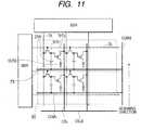
- FIG. 11is a block diagram to further explain the arrangement of the display module as shown in FIG. 9, which module is provided with the pixel arrangement as shown in FIG. 10.
- the drain of the TFT 2is connected to a current supply line CSL while the source thereof is connected to a first electrode (positive electrode herein) AD of the organic light emitting diode OLED.
- the other electrode (negative pole) of the capacitor CPRis connected to the common voltage line COML ramified from the common voltage supply bus line COMB.
- the data line DLis driven by the data driving circuit DDR while the scanning line (or gate line) GL is driven by the gate driving circuit GDR.
- a current supply line CSLis connected to an external power source via a current supply bus line CSLB and by way of either a current supply circuit CSS as shown in FIG. 9 or a terminal.
- the operation level of the capacitor CPRis regulated by the electric potential of the common voltage line COML, which controls the light emitting behavior of the pixel.
- the current issued out of the OLEDflows from the cathode CD thereof to a current drain line that is not shown in the drawings.
- the above systemrequires the provision of the common voltage line that gets through a portion of the pixel region, which causes the deterioration of a so-called aperture ratio and constraints the displaying brightness of the module on the whole from improving.
- FIG. 12is a block diagram to show another example of the prior OLED display module in the similar arrangement to that as shown in FIG. 11.
- the basic alignment of the TFT 1 and TFT 2 and the capacitor CPR comprising the respective pixelsis the same as shown in FIG. 9, the difference with which lies in the fact that the other end of the capacitor CPR is connected to the current supply line CSL.
- the source electrode of the TFT 2 equivalent to the first electrode (anode, for example, which is also referred to as the first electrode layer hereinafter) AD of the OLEDis formed of a conductive thin film made from such as ITO (Indium Tin Oxide) and the first electrodes AD of the respective pixels PX are individually separated from one another.
- ITOIndium Tin Oxide
- the second electrode thereof CDcomprising an emitting device (cathode, for instance, which is also referred to as the second electrode layer hereinafter) locates at the uppermost position of the diode so as to be exposed to the air, which might cause corrosion thereon.
- the second electrode layersare made of a film uniformly formed over the whole pixels, which requires electrical connection with an external circuit.
- a terminal that is intended for supplying electric current to this second electrode layer CDis extensively led out to the terminal section (terminal pad) of the substrate from the same layer, the vicinity of that terminal section is prone to corrosion owing to exposure to the air.
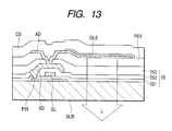
- FIG. 13is a sectional view of the structure of the vicinity of one pixel of the OLED display module.
- This display moduleis arranged by stacking up on the glass substrate SUB a polysilicone or preferably low temperature polysilicone semiconductor layer PSI, a first insulating layer IS 1 , a scanning or gate line (gate electrode) GL, a second insulating layer IS 2 , a source electrode SD formed of aluminum wiring, a third insulating layer IS 3 , a passivation film PSV, a first electrode layer AD, an organic emitting layer OLE and a second electrode layer CD one over another in this order.
- a polysilicone or preferably low temperature polysilicone semiconductor layer PSIa first insulating layer IS 1 , a scanning or gate line (gate electrode) GL, a second insulating layer IS 2 , a source electrode SD formed of aluminum wiring, a third insulating layer IS 3 , a passivation film PSV, a first electrode layer AD, an organic emitting
- the organic emitting devicecomprising the first electrode AD in connection with the source electrode SD, the organic emitting layer OLE and the second electrode layer CD emits light, which light L is emitted out of the substrate SUB.
- the currentis insufficiently supplied thereto or detours the said pixel so as to cause insufficient or null light emission, which results in such display faults as a so-called dot or region defect.
- the present inventionis to provide a display module that allows image to be displayed with high quality by improving a power supply mechanism to the second electrode layers comprising the pixels so as to prevent the same layers from being corroded.
- the present inventionis arranged such that an electrode layer in connection with the second layer is provided on the substrate wherein the electrode layer is connected to the second electrode layer through a contact hole and the outgoing line of the second electrode layer is an underlying wiring coated with a passivation film on the substrate.
- This arrangementprovides a display module of high credibility that prevents cathode from being corroded and allows image to be displayed with high quality.
- the characteristic features of the display module according to the present inventionlie in that:
- a pixelis provided in the respective intersections between a plurality of scanning lines and a plurality of data lines, which lines are aligned in a matrix within a display region on a substrate and a current supply line is provided to supply said pixel with current for display, wherein said pixel is provided with an active device that is selected by the scanning line, a data storage device that stores a data signal supplied from said data line when the active device is put into on-state condition and an emitting device that emits light by current supplied from the current supply line according to the data signal stored in the data storage device, wherein said emitting device comprises a first electrode layer, an organic emitting layer coated over the first electrode layer and a second electrode layer formed on the organic emitting layer, wherein an electrode layer is provided on the substrate, which layer is lower than the second electrode layer and coated with an insulating or passivation film and to which layer the second electrode layer is connected through a contact hole.
- the arrangement (1)further includes a first terminal pad that supplies the data signal to a data driving circuit from an external circuit, a second terminal pad that supplies a gate signal to a gate driving circuit and a third terminal pad that supplies current to a current supply bus line and a fourth terminal pad that connects the electrode layer in connection with the second electrode layer, which pads are provided in an outside of the display region of the substrate.
- the arrangement (2)further includes a current supply wiring that connects the current supply bus line commonly connecting the current supply lines to the third terminal pad and a wiring that connects the electrode layer in connection with the second electrode layer to the fourth terminal pad.
- Either the arrangement (1) or (2)is characterized in that the first to fourth terminal pads are provided in one side of the substrate.
- the arrangement (4)is further characterized in that the current supply wiring and the wiring that connects the electrode layer in connection with the second electrode layer to the fourth terminal pad are provided in a side adjacent to the said one side of the substrate.
- the arrangement (4)is further characterized in that the current supply wiring and the wiring that connects the electrode layer in connection with the second electrode layer to the fourth terminal pad are provided in respective sides adjacent to the said one side of the substrate.
- Either the arrangement (1) or (2)is further characterized in that the third and fourth terminal pads are provided in a first side of the substrate opposed to a second side thereof in which the first and second terminal pads are provided.
- any one of the arrangements (2) to (7)is characterized in that the electrode layer in connection with the second electrode layer is provided outer than the current supply bus line commonly connecting the current supply lines on the substrate.
- any one of the arrangements (2) to (7)is characterized in that the electrode layer in connection with the second electrode layer is provided outer than the current supply wiring connected to the current supply bus line on the substrate.
- FIG. 1is a block diagram to show the arrangement of a first embodiment of the display module according to the present invention.
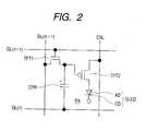
- FIG. 2is a view to show the arrangement of the pixel circuit corresponding to one pixel of the display module as shown in FIG. 1.
- FIG. 3is a view to show the vicinity of one pixel for explaining the light emitting mechanism of the display module according to the present invention.
- FIG. 4is a view to show the state where the second electrode layer and the electrode layer in connection therewith are connected.
- FIG. 5is a block diagram to show the arrangement of a second embodiment of the display module according to the present invention.
- FIG. 6is a block diagram to show the arrangement of a third embodiment of the display module according to the present invention.
- FIG. 7is a block diagram to show the arrangement of a fourth embodiment of the display module according to the present invention.
- FIG. 8is a block diagram to show the arrangement of a fifth embodiment of the display module according to the present invention.
- FIG. 9is a block diagram to show the arrangement of one example of the prior OLED display module.
- FIG. 10is a view to show the arrangement of the pixel of the display module as shown in FIG. 9.
- FIG. 11is a block diagram to show the arrangement of the display module as shown in FIG. 9 and provided with the pixel arrangement as shown in FIG. 10 in more details.
- FIG. 12is a block diagram like FIG. 11 to show the arrangement of another example of the prior OLED display module.
- FIG. 13is a sectional view to show the arrangement of the vicinity of one pixel of an OLED display module.
- the organic emitting layer of the respective pixels as described belowis divided into one type that emits light with luminance in proportion to the value of the current and with a color (including white) inherent in an organic material in use so as to display monochrome or color image and the other type that incorporates a red, green, blue or other color filter into the organic layer to emit white light so as to display color image.
- FIG. 1is a block diagram to show the arrangement of the first embodiment of the display module according to the present invention.
- the display module of this embodimentis provided with a gate driving circuit GDR and a data driving circuit DDR on the glass substrate SUB thereof.
- one pixelis formed within the region surrounded by scanning lines GL that are driven or scanned by the gate driving circuit GDR and a data line DL that is driven by the data driving circuit DDR, which lines are aligned in a matrix, and a current supply line CSL.
- terminal pads PAD 1 and PAD 2are provided to supply signals and voltage to the gate driving circuit GDR and the data driving circuit DDR from an external circuit.
- FIG. 2is a view to show the arrangement of the pixel circuit corresponding to one pixel of the display module as shown in FIG. 1.
- one pixelis formed within the region surrounded by a data line DL (m+1), scanning lines GL (n+1) and GL (n) as well as the current supply line CSL. It is supposed herein that the scanning line that is being scanned or selected is the GL (n+1).
- the first thin film transistor TFT 1is a switching transistor while the second thin film transistor TFT 2 is a driver transistor, which transistors are active devices.
- the gate of the TFT 1is connected to the scanning line GL (n+1) while the drain thereof is connected to the data line DL (m+1) and the source thereof is connected to the gate of the TFT 2 .
- the drain of the TFT 2is connected to the current supply line CSL, to which line the current is supplied from a current supply bus line CSB as shown in FIG. 1 while the source thereof is connected to a first electrode layer AD of an organic light emitting diode OLED.
- One terminal of a capacitor CPR serving as a data signal storage deviceis connected to a point where the source of the TFT 1 and the gate of the TFT 2 connect while the other terminal thereof is connected to the scanning line GL (n) right in front of the same.
- one terminal of the capacitor CPR that is connected to a point where the source of the TFT 1 and the gate of the TFT 2 connectis of positive pole while the other terminal thereof that is connected to the scanning line GL (n) is of negative pole.
- the organic light emitting diode OLEDis arranged by interposing an organic emitting layer, which is not shown in the drawings, between the first electrode layer AD and a second electrode layer CD wherein the first electrode layer AD is connected to the source of the TFT 2 while the second electrode layer CD, which layer is uniformly formed over the whole pixels, is connected to an electrode layer in connection with the second electrode layer CNTB as shown in FIG. 1.
- the electrode layer CNTBis a so-called current drain line (electrode), which layer is formed in a lower layer of the substrate or in the same layer as the terminal pads PAD 1 and PAD 2 and is connected to the second electrode layer CD through a contact hole CNT as well as to the terminal pad PAD 4 formed in the same layer as the terminal pads PAD 1 and PAD 2 through a wiring CNTL.
- electrodecurrent drain line
- the current supply line CSL that is a wiring of the first electrode layeris connected through a current supply bus line CSB and a current supply wiring CSLL to the terminal pad PAD 3 formed in the same layer as the terminal pads PAD 1 and PAD 2 .
- the electrode layer in contact with the second electrode layer CNTBis disposed on the substrate outer than the current supply bus line CSB and within a sealing area SL thereof as shown with the dotted line in the drawing.
- the electrode layer CNTB in contact with the second electrode layer CD through the contact hole CNTis disposed on the substrate outer than the current supply bus line CSB and within the sealing area thereof facilitates the layout design on a substrate especially when the internal circuits on a flexible print substrate are connected to the external circuit at one side thereof.
- the data signalwhich is written into the capacitor CPR and stored therein as charge amount when the TFT 1 is put into on-state condition, flows electric current supplied from the current supply line CSL as the quantity of current controlled by the charge amount (indicating the gray scale of the data signal) as stored in the capacitor CPR to the organic light emitting diode OLED when the TFT 2 turns into on-stage condition while the TFT 1 is put into off-state condition.
- the organic light emitting diode OLEDemits light with luminance in proportion to the quantity of current as supplied and with a color inherent in the organic emitting layer material in use.
- the organic emitting layer materialchanges for the respective pixels of red, green and blue or the color filters of the respective colors are incorporated into the organic emitting layer material to emit white light.
- the data signalmay be supplied in analog quantity or in time sharing digital quantity.
- the gray scale controlmay incorporate an area gray scale system wherein the pixel areas of red, green and blue respectively are divided.
- the present embodimentis arranged such that the current flowing out of the current supply bus line CSB and the second electrode layer CD after the light emitting operation of the respective pixel circuits is discharged from the electrode layer CNTB or the current drain line, which layer or line is formed in a lower layer of the substrate and over the whole pixels, to the external circuit through the wiring CNTL and the terminal pad PAD 4 .
- the second electrode layer CD common in the whole pixels that is uniformly formed in an upper layer of the substrateis connected through he contact hole CNT to the electrode layer CNTB.
- the wiring CNTLis formed in the same layer as the electrode layer CNTB.
- the display module of this kindadopts a sealing structure by means of a can, for instance, in order to secure its function credibility.
- the sealing areais provided for attaching such sealing can thereon, within which area the electrode layer CNTB and the wiring CNTL are disposed.
- The, at least the electrode layer CNTBis disposed outer than the current supply bus line CSB.
- the electrode layer CNTB and so forth as mentioned aboveare formed in a lower layer of the substrate, on which an insulating or passivation film is laminated so that there is no case where the second electrode, the electrode layer in contact therewith preferably including the wiring CNTL have no contact with the air, which prevents them from being corroded and improves credibility, with the result that a display module with high quality display can be provided.
- the contact hole as mentioned abovemay well be only one, but the plurality of the contact holes are provided herein for the purpose of stably supplying as much current as possible.
- FIG. 3is a view to show the vicinity of one pixel for the purpose of explaining the light emitting mechanism of the display module according to the present invention.
- FIG. 4is a view to show the contact portion between the second electrode layer and the electrode layer in contact therewith.
- the same references of FIG. 1correspond to the same elements.
- the arrow as indicated with the reference I in the drawingstracks the course of the current that contributes to the light emitting behavior.
- the TFT 2is a driver transistor. Upon the selection of this TFT 2 by the gate line GL, the current I having a value of the gray scale corresponding to the data signal as stored in the capacitor CPR is supplied from the current supply line ramified from the current supply bus line to the first electrode layer AD of the organic light emitting diode OLED through the TFT 2 .
- the organic light emitting diode OLEDemits light L having a spectrum corresponding to the emitting layer material OLE such that the electrons from the second electrode layer CD and the holes of the first electrode layer AD are rejoined inside the emitting layer OLE.
- the first electrode layers AD of the respective pixelsare independent from each other while the second electrode layer CD is uniformly formed over the whole pixels.
- the current I conducted through the OLED from the TFT 2flows out to the terminal pad PAD 4 via the wiring CNTL as shown in FIG. 1 by way of the second electrode layer CD and the electrode layer CNTB in contact therewith.
- a number of pixels as arranged aboveare aligned in a matrix so as to provide a two-dimensional display module.
- FIG. 5is a block diagram to show the arrangement of the second embodiment of the display module according to the present invention.
- This embodimentis arranged such that the two terminal pads PAD 3 and PAD 3 ′ of the current supply bus line CSB connecting the current supply lines CSL as well as the terminal pad PAD 4 of the electrode layer in contact with the second electrode layer CNTB are provided in a side of the substrate as opposed to that where the terminal pad PAD 1 of the data driving circuit and the terminal pad PAD 2 of the gate driving circuit GDR are provided.
- the electrode layer CNTB in contact with the second electrode layer CD through the contact hole CNTis disposed on the substrate SUB outer than the current supply bus line CSB and within the sealing area thereof facilitates the layout design on the substrate.
- the current supply wiring CSLL between the current supply bus line CSB and the terminal pads PAD 3 and PAD 3 ′ thereofbecomes short in length on the substrate, which allows the current to be more uniformly supplied and drained. This makes the light emitting distribution within the display region uniform, which allows image to be displayed with high quality.
- two sets of the current supply wiring CSLLare exemplified in this embodiment, but it may be any one of them. In the event where the current supply wiring CSLL is led out of the respective ends of the current supply bus line CSB, it brings a good effect on symmetry.
- the electrode layer CNTB in contact with the second electrode layer CD through the contact hole CNTis disposed on the substrate outer than the current supply bus line CSB and within the sealing region thereof facilitates the layout design on a substrate especially when the internal circuits are connected to the external circuit at the opposed two sides of the flexible print substrate.
- the arrangement of the present embodimentallows the wiring pattern in the vicinity of the sealing region to reduce, which gets rid of obstacles to block UV rays upon the solidification of a sealing material so as to cause the sealing material to be effectively hardened. This secures the sealing of the module, which leads to the improved credibility thereof.
- FIG. 6is a block diagram to show the arrangement of the third embodiment of the display module according to the present invention.
- the same references of FIG. 1correspond to the same elements.
- the present embodimentis arranged such that the terminal pad PAD 3 of the current supply bus line CSB connecting the current supply lines CSL and the terminal pad PAD 4 of the electrode layer CNTB in contact with the second electrode layer are separately provided in the respective ends of one side of the substrate where the terminal pad PAD 1 of the data driving circuit and the terminal pad PAD 2 of the gate driving circuit GDR are disposed.
- the electrode layer CNTB in contact with the second electrode layer CD through the contact hole CNTis disposed on the substrate outer than the current supply bus line CSB and within the sealing region thereof.
- the other arrangements hereofare the same as those of the first one as shown in FIG. 1, the explanation of which is omitted to avoid redundancy.
- the electrode layer CNTB in contact with the second electrode layer CD through the contact hole CNTis disposed on the substrate outer than the current supply bus line CSB and within the sealing region thereof facilitates the layout design especially when the internal circuits are connected to the external circuit at one side of the flexible print substrate.
- FIG. 7is a block diagram to shown the arrangement of the fourth embodiment of the display module according to the present invention.
- the same references of FIG. 1correspond to the same elements.
- the present embodimentis arranged such that the terminal pad PAD 3 of the current supply bus line CSB connecting the current supply lines CSL and the terminal pad PAD 4 of the electrode layer CNTB in contact with the second electrode layer are provided in a side of the substrate as opposed to one side thereof where the terminal pad PAD 1 of the data driving circuit and the terminal pad PAD 2 of the gate driving circuit GDR are disposed.
- the electrode layer CNTB in contact with the second electrode layer CD through the contact hole CNTis disposed on the substrate outer than the current supply bus line CSB and within the sealing region thereof.
- the arrangement hereof that the electrode layer CNTB in contact with the second electrode layer CD through the contact hole CNTis disposed on the substrate outer than the current supply bus line CSB and within the sealing region thereof facilitates the layout on a substrate especially when the internal circuits are connected to the external circuit at the opposed two sides of the flexible print substrate.
- the other arrangements hereofare the same as the third embodiment as shown in FIG. 6 , the explanation of which is omitted for redundancy.
- the current supply wiring CSLL between the current supply bus line CSB and the terminal pad PAD 3 thereof and the wiring CNTL between the electrode layer CNT in contact with the second electrode layer CD and the terminal pad PAD 4 thereofbecome short in length, which allows the current to be uniformly supplied and be drained. This makes the light emitting distribution within the display region uniform, which allows image to be displayed with high quality.
- the arrangement hereofallows the wiring pattern in the vicinity of the sealing area to reduce so as to get rid of obstacles to block UV rays upon the solidification of a sealing material, with the result that the sealing material can be effectively hardened. This makes the sealing of the module so as to further improve the credibility of the same.
- the current supply wiring CSLL and the wiring CNTL that amount to the course of the currentoccupy a wide area on the substrate with sufficient dimension in thickness, which makes the said secure and stable. Further, especially in the second and fourth embodiments wherein the distance with the terminal pads is short in length, it secures more stable course of the current.
- FIG. 8is a block diagram to show the arrangement of the fifth embodiment of the display module according to the present invention
- the same references of FIG. 1correspond to the same elements.
- the present embodimentis arranged such that the electrode layer CNTB in contact with the second electrode layer is disposed in a side of the substrate, which side is adjacent to the side thereof where the terminal pads PAD 1 to PAD 4 are disposed and is as opposed to the side thereof where the gate driving circuit GDR is disposed, and outer than the current supply wiring CSLL.
- the wiring CNTL between the electrode layer CNTB and the terminal pad PAD 4 thereofbecomes short in length so as to allow the current to be uniformly supplied and drained. This makes the light emitting distribution within the display region uniform, which allows image to be displayed with high quality.
- the first and second electrode layersrespectively correspond to the cathode layer and the anode layer which can also correspond to vice versus in the present invention.
- the present inventionis not limited to the OLED display module as mentioned above, but it is also applicable to other display modules that perform the same emitting operation as the OLED counterpart.
- the electrode layers comprising the pixels of the display module and the vicinity of the terminal pads thereofare prevented from corrosion so as to dispense with display faults. Further, the current is stably and sufficiently supplied through the current supply line, so that the display module that allows image to be displayed with high quality is provided.
Landscapes
- Engineering & Computer Science (AREA)
- Physics & Mathematics (AREA)
- General Physics & Mathematics (AREA)
- Theoretical Computer Science (AREA)
- Computer Hardware Design (AREA)
- Microelectronics & Electronic Packaging (AREA)
- Optics & Photonics (AREA)
- Geometry (AREA)
- Electroluminescent Light Sources (AREA)
- Devices For Indicating Variable Information By Combining Individual Elements (AREA)
Abstract
Description
- The present invention relates to an active matrix display module, especially, pertaining to such display module as being provided with pixels comprising such emitting devices as an EL (electro luminescence) device or a LED (light emitting diode) wherein light is emitted by conducting electric current through such an emitting layer as an organic semiconductor thin film and with pixels circuits to control the emitting operation of those pixels.[0001]
- Recently, the advent of advanced information network system in our modern life increases the demand for personal computers, car navigation systems, portable remote terminals and communication network equipment or the combined products thereof. For such products as mentioned above, such a display device as being thin in thickness, light in weight and of lower power consumption is suitable so that a liquid crystal display or a display module incorporating such electrooptic devices as a self-luminous EL device or LED therein are in practical use.[0002]
- The latter display module is characterized in being good at visibility, possessed with wide viewing angle and being suitable for motion display due to its high response, which module is said to especially opt for image display. In particular, a display incorporating an organic EL device (also referred to as an organic LED device; hereinafter, referred to as OLED in abbreviation, where appropriate), the emitting layer of which device is made from organic matter, is highly expectable in accordance with the greater improvement of the luminous efficiency thereof and the progress of the network technology that enhances the feasibility of image communication. The OLED display is of diode structure in which an organic emitting layer is interposed between two pieces of electrodes.[0003]
- As described below, the active matrix driving method in which thin film transistors (hereinafter, referred to as TFT where appropriate) serve as the switching devices of pixels is effective for enhancing the power efficiency of such OLED display as mentioned above. The operation of the OLED display by the active matrix driving method in the prior arts is disclosed in the Japanese Patent Application Laid-open Nos. HEI 4-328791 and 8-241048 or the U.S. Pat. No. 5,550,066, for instances, the driving voltage of which display is disclosed in the International Publication No. WO98/36407 and so forth.[0004]
- The typical pixel structure of the OLED display comprises two thin film transistors or TFTs equivalent to a first and a second active devices, the first of which is a switching transistor while the second of which is a driver transistors and a pixel driving circuit (hereinafter, referred to as a pixel circuit where appropriate) comprising one capacitor for a data signal storage device, which pixel circuit controls the emitting luminance of the OLED display. The pixels are disposed at the respective intersections of a matrix in which the data lines having M in number to which data signals (or image signals) are supplied and the scanning lines (hereinafter, referred to as gate lines where appropriate) having N in number are aligned in the arrangement of N lines×M rows.[0005]
- To drive the pixels, the scanning signals (gate signals) are subsequently supplied to the gate lines having N in number so as to put the switching transistors into on-state condition, and one time of the vertical scanning operation is over within one frame period of Tf so as to freshly supply the on-state voltage to the first gate line.[0006]
- In the above driving method, the time required for supplying the on-state voltage to one gate line is defined as Tf/N or below. Generally, the value of the one frame period of Tf is in the order of {fraction (1/60)} second in practical use. It should be noted that where one frame period is represented with two fields, one field period becomes equivalent to one half of the one frame period.[0007]
- During the on-state voltage is supplied to a certain gate line, all the switching transistors that are connected to the corresponding data line are put into on-state condition, in synchronization with which the data voltage (image voltage) is simultaneously or subsequently supplied to the data lines having M rows in number, which arrangement is general in the active matrix liquid crystal display.[0008]
- The data voltage, during the on-state voltage (hereinafter, referred to as “on” while the off-state is referred to as “off” where appropriate) is supplied to the gate line, is stored in storage capacitance (capacitor) so as to be maintained substantially as it is during the one frame period (or one field period). The voltage value of the storage capacitance regulates the gate voltage of the driver transistor.[0009]
- Accordingly, the value of the current flowing through the driver transistor is controlled so as to put the light emission of the OLED under control. The response time for the OLED to begin emitting light upon the application of voltage thereto normally takes one is or below so that it manages to follow the motion image of quick tempo. A current supply line is provided in order to supply the driver transistor with current, from which line the current for display in response to the data signal as stored in the storage capacitance is supplied.[0010]
- The active matrix driving method realizes high efficient operation by performing light emission over the one frame period. The difference with the passive matrix driving method, in which the respective electrodes of the OLED diode are directly connected to the scanning line and the data line without the provision of any TFTs, is clear as follows.[0011]
- In the passive matrix driving method, the current flows through the OLED only during the short period when the scanning line is selected, so that emitting luminance corresponding to practically several times as many as the number of the scanning lines is required for obtaining the same luminance as that of the one frame period of the active matrix driving method with the light emission performed during such short period as mentioned above. Thus, it is unavoidable that the driving voltage and current in use enlarge, which causes large loss of power consumption such as heating so as to deteriorate power efficiency.[0012]
- In view of the foregoing, it is found that the active matrix driving method is superior to the passive one in light of the reduction of power consumption.[0013]
- The passive matrix driving display module as described above is provided with terminal pads that are intended for leading the scanning lines and data lines as a whole as crosswise disposed in a display region on the substrate out of the same region so as to be connected to a driving circuit, which circuit is connected to an external circuit. However, such terminal arrangement is hard to apply to an active matrix driving display module.[0014]
- That is, the active matrix driving OLED display module is arranged such that current supply to capacitors to keep display over one frame period is carried out by connecting one electrode thereof to an output terminal of the switching transistors while connecting the other electrode thereof to either a common voltage line for the capacitors or a current supply line that supplies current to an OLED.[0015]
- FIG. 9 is a block diagram to show one example of the prior OLED display module while FIG. 10 is an explanatory view to show the pixel arrangement of the module as shown in FIG. 9. This display module (image display module) is arranged on a substrate SUB made from such insulating material as glass such that a data driving circuit DDR, a gate driving circuit GDR and a current supply circuit CSS are disposed in the surrounding of a display section AR as surrounded by the dotted line in the drawing, in which section the plurality of data lines DL and the plurality of gate lines GL are aligned in a matrix.[0016]
- The data driving circuit DDR includes a complementary circuit of an NP-channels thin film transistor TFT or a shift register circuit, a level shifter circuit and an analog switch circuit comprising a single (N or P) channel thin film transistor TFT. To note, the current supply circuit CSS may be modified into just a bus line while the current may be supplied from an external power source.[0017]
- FIG. 9 shows a system in which a common voltage line COML for the capacitors is provided in the display section AR, to which common voltage line COML the other electrodes of the capacitors are connected. The common voltage line COML is led out to an external common voltage source from a terminal COMT of a common voltage supply bus line COMB. To note, another system is also known, in which system the capacitors are connected to a current supply line without the provision of the common voltage line.[0018]
- As shown in FIG. 10, a pixel PX comprises a first thin film transistor TFT[0019]1 or a switching transistor, a second thin film transistor TFT2 or a driver transistor, a capacitor CPR and an organic light emitting diode OLED, which are disposed in the region surrounded by the data line DL and the gate line GL. The gate of the TFT1 is connected to the gate line GL while the drain thereof is connected to the data line DL. The gate of the TFT2 is connected to a source of the TFT1, to which source one electrode (positive pole) of the capacitor CPR is connected.
- FIG. 11 is a block diagram to further explain the arrangement of the display module as shown in FIG. 9, which module is provided with the pixel arrangement as shown in FIG. 10. The drain of the TFT[0020]2 is connected to a current supply line CSL while the source thereof is connected to a first electrode (positive electrode herein) AD of the organic light emitting diode OLED. The other electrode (negative pole) of the capacitor CPR is connected to the common voltage line COML ramified from the common voltage supply bus line COMB. The data line DL is driven by the data driving circuit DDR while the scanning line (or gate line) GL is driven by the gate driving circuit GDR. A current supply line CSL is connected to an external power source via a current supply bus line CSLB and by way of either a current supply circuit CSS as shown in FIG. 9 or a terminal.
- In FIGS. 10 and 11, when the TFT[0021]1 is put into on-state condition upon the selection of one pixel PX by the gate line GL, a video signal supplied from the data line DL is stored in the capacitor CPR. Then, when the TFT1 is put into off-state condition, the TFT2 turns into on-state condition so that the current flows from the CSL to the OLED, which current keeps intact practically over one frame period. The current in conduction at this time is regulated by a signal charge stored in the capacitor.
- The operation level of the capacitor CPR is regulated by the electric potential of the common voltage line COML, which controls the light emitting behavior of the pixel. The current issued out of the OLED flows from the cathode CD thereof to a current drain line that is not shown in the drawings.[0022]
- The above system requires the provision of the common voltage line that gets through a portion of the pixel region, which causes the deterioration of a so-called aperture ratio and constraints the displaying brightness of the module on the whole from improving.[0023]
- FIG. 12 is a block diagram to show another example of the prior OLED display module in the similar arrangement to that as shown in FIG. 11. The basic alignment of the TFT[0024]1 and TFT2 and the capacitor CPR comprising the respective pixels is the same as shown in FIG. 9, the difference with which lies in the fact that the other end of the capacitor CPR is connected to the current supply line CSL.
- That is, when the TFT[0025]1 is put into on-state condition upon the selection of one pixel by the gate line GL, a video signal supplied from the data line DL is stored in the capacitor CPR, and when the TFT2 turns into on-state condition while the TFT1 is put into off-state condition, the current flows from the CSL to the OLED, which current keeps intact practically over one frame period (or one field period) in the same way as the example shown in FIG. 10. The current in conduction at this time is regulated by a signal charge stored in the capacitor CPR. The operation level of the capacitor is regulated by the electric potential of the current supply line CSL, which controls the light emitting behavior of the pixel.
- In the prior display modules as described above with reference to FIGS. 9 through 12, the source electrode of the TFT[0026]2 equivalent to the first electrode (anode, for example, which is also referred to as the first electrode layer hereinafter) AD of the OLED is formed of a conductive thin film made from such as ITO (Indium Tin Oxide) and the first electrodes AD of the respective pixels PX are individually separated from one another.
- The second electrode thereof CD comprising an emitting device (cathode, for instance, which is also referred to as the second electrode layer hereinafter) locates at the uppermost position of the diode so as to be exposed to the air, which might cause corrosion thereon. Normally, the second electrode layers are made of a film uniformly formed over the whole pixels, which requires electrical connection with an external circuit. In the event where a terminal that is intended for supplying electric current to this second electrode layer CD is extensively led out to the terminal section (terminal pad) of the substrate from the same layer, the vicinity of that terminal section is prone to corrosion owing to exposure to the air.[0027]
- FIG. 13 is a sectional view of the structure of the vicinity of one pixel of the OLED display module. This display module is arranged by stacking up on the glass substrate SUB a polysilicone or preferably low temperature polysilicone semiconductor layer PSI, a first insulating layer IS[0028]1, a scanning or gate line (gate electrode) GL, a second insulating layer IS2, a source electrode SD formed of aluminum wiring, a third insulating layer IS3, a passivation film PSV, a first electrode layer AD, an organic emitting layer OLE and a second electrode layer CD one over another in this order.
- Upon the selection of the thin film transistor (or driver transistor) comprising the polysilicone semiconductor layer PSI, the gate line GL and the source electrode SD, the organic emitting device comprising the first electrode AD in connection with the source electrode SD, the organic emitting layer OLE and the second electrode layer CD emits light, which light L is emitted out of the substrate SUB.[0029]
- In this case, provided that there is corrosion or degradation partially found on the second electrode layer CD of the said pixel, the current is insufficiently supplied thereto or detours the said pixel so as to cause insufficient or null light emission, which results in such display faults as a so-called dot or region defect.[0030]
- The present invention is to provide a display module that allows image to be displayed with high quality by improving a power supply mechanism to the second electrode layers comprising the pixels so as to prevent the same layers from being corroded.[0031]
- To achieve this purpose, the present invention is arranged such that an electrode layer in connection with the second layer is provided on the substrate wherein the electrode layer is connected to the second electrode layer through a contact hole and the outgoing line of the second electrode layer is an underlying wiring coated with a passivation film on the substrate.[0032]
- This arrangement provides a display module of high credibility that prevents cathode from being corroded and allows image to be displayed with high quality. The characteristic features of the display module according to the present invention lie in that:[0033]
- (1) A pixel is provided in the respective intersections between a plurality of scanning lines and a plurality of data lines, which lines are aligned in a matrix within a display region on a substrate and a current supply line is provided to supply said pixel with current for display, wherein said pixel is provided with an active device that is selected by the scanning line, a data storage device that stores a data signal supplied from said data line when the active device is put into on-state condition and an emitting device that emits light by current supplied from the current supply line according to the data signal stored in the data storage device, wherein said emitting device comprises a first electrode layer, an organic emitting layer coated over the first electrode layer and a second electrode layer formed on the organic emitting layer, wherein an electrode layer is provided on the substrate, which layer is lower than the second electrode layer and coated with an insulating or passivation film and to which layer the second electrode layer is connected through a contact hole.[0034]
- (2) The arrangement (1) further includes a first terminal pad that supplies the data signal to a data driving circuit from an external circuit, a second terminal pad that supplies a gate signal to a gate driving circuit and a third terminal pad that supplies current to a current supply bus line and a fourth terminal pad that connects the electrode layer in connection with the second electrode layer, which pads are provided in an outside of the display region of the substrate.[0035]
- (3) The arrangement (2) further includes a current supply wiring that connects the current supply bus line commonly connecting the current supply lines to the third terminal pad and a wiring that connects the electrode layer in connection with the second electrode layer to the fourth terminal pad.[0036]
- (4) Either the arrangement (1) or (2) is characterized in that the first to fourth terminal pads are provided in one side of the substrate.[0037]
- (5) The arrangement (4) is further characterized in that the current supply wiring and the wiring that connects the electrode layer in connection with the second electrode layer to the fourth terminal pad are provided in a side adjacent to the said one side of the substrate.[0038]
- (6) The arrangement (4) is further characterized in that the current supply wiring and the wiring that connects the electrode layer in connection with the second electrode layer to the fourth terminal pad are provided in respective sides adjacent to the said one side of the substrate.[0039]
- (7) Either the arrangement (1) or (2) is further characterized in that the third and fourth terminal pads are provided in a first side of the substrate opposed to a second side thereof in which the first and second terminal pads are provided.[0040]
- (8) Any one of the arrangements (2) to (7) is characterized in that the electrode layer in connection with the second electrode layer is provided outer than the current supply bus line commonly connecting the current supply lines on the substrate.[0041]
- (9) Any one of the arrangements (2) to (7) is characterized in that the electrode layer in connection with the second electrode layer is provided outer than the current supply wiring connected to the current supply bus line on the substrate.[0042]
- It should be appreciated that the present invention is not limited to the above arrangements and the embodiments as described below, but it can be modified into various manners within the scope of the accompanying patent claims. The other objects and arrangements of the present invention are clarified from the following description.[0043]
- FIG. 1 is a block diagram to show the arrangement of a first embodiment of the display module according to the present invention.[0044]
- FIG. 2 is a view to show the arrangement of the pixel circuit corresponding to one pixel of the display module as shown in FIG. 1.[0045]
- FIG. 3 is a view to show the vicinity of one pixel for explaining the light emitting mechanism of the display module according to the present invention.[0046]
- FIG. 4 is a view to show the state where the second electrode layer and the electrode layer in connection therewith are connected.[0047]
- FIG. 5 is a block diagram to show the arrangement of a second embodiment of the display module according to the present invention.[0048]
- FIG. 6 is a block diagram to show the arrangement of a third embodiment of the display module according to the present invention.[0049]
- FIG. 7 is a block diagram to show the arrangement of a fourth embodiment of the display module according to the present invention.[0050]
- FIG. 8 is a block diagram to show the arrangement of a fifth embodiment of the display module according to the present invention.[0051]
- FIG. 9 is a block diagram to show the arrangement of one example of the prior OLED display module.[0052]
- FIG. 10 is a view to show the arrangement of the pixel of the display module as shown in FIG. 9.[0053]
- FIG. 11 is a block diagram to show the arrangement of the display module as shown in FIG. 9 and provided with the pixel arrangement as shown in FIG. 10 in more details.[0054]
- FIG. 12 is a block diagram like FIG. 11 to show the arrangement of another example of the prior OLED display module.[0055]
- FIG. 13 is a sectional view to show the arrangement of the vicinity of one pixel of an OLED display module.[0056]
- Hereinafter, the preferred embodiments of the present invention are described in details with reference to the accompanying drawings. The organic emitting layer of the respective pixels as described below is divided into one type that emits light with luminance in proportion to the value of the current and with a color (including white) inherent in an organic material in use so as to display monochrome or color image and the other type that incorporates a red, green, blue or other color filter into the organic layer to emit white light so as to display color image.[0057]
- FIG. 1 is a block diagram to show the arrangement of the first embodiment of the display module according to the present invention. The display module of this embodiment is provided with a gate driving circuit GDR and a data driving circuit DDR on the glass substrate SUB thereof.[0058]
- Then, one pixel is formed within the region surrounded by scanning lines GL that are driven or scanned by the gate driving circuit GDR and a data line DL that is driven by the data driving circuit DDR, which lines are aligned in a matrix, and a current supply line CSL. In one side of the substrate SUB, terminal pads PAD[0059]1 and PAD2 are provided to supply signals and voltage to the gate driving circuit GDR and the data driving circuit DDR from an external circuit.
- FIG. 2 is a view to show the arrangement of the pixel circuit corresponding to one pixel of the display module as shown in FIG. 1. In the present embodiment, one pixel is formed within the region surrounded by a data line DL (m+1), scanning lines GL (n+1) and GL (n) as well as the current supply line CSL. It is supposed herein that the scanning line that is being scanned or selected is the GL (n+1).[0060]
- Attention is paid to one pixel PX among the plurality of pixels as selected by the scanning line GL (n+1). The first thin film transistor TFT[0061]1 is a switching transistor while the second thin film transistor TFT2 is a driver transistor, which transistors are active devices. The gate of the TFT1 is connected to the scanning line GL (n+1) while the drain thereof is connected to the data line DL (m+1) and the source thereof is connected to the gate of the TFT2.
- The drain of the TFT[0062]2 is connected to the current supply line CSL, to which line the current is supplied from a current supply bus line CSB as shown in FIG. 1 while the source thereof is connected to a first electrode layer AD of an organic light emitting diode OLED. One terminal of a capacitor CPR serving as a data signal storage device is connected to a point where the source of the TFT1 and the gate of the TFT2 connect while the other terminal thereof is connected to the scanning line GL (n) right in front of the same.
- In the arrangement of one pixel circuit as shown in FIG. 2, one terminal of the capacitor CPR that is connected to a point where the source of the TFT[0063]1 and the gate of the TFT2 connect is of positive pole while the other terminal thereof that is connected to the scanning line GL (n) is of negative pole.
- The organic light emitting diode OLED is arranged by interposing an organic emitting layer, which is not shown in the drawings, between the first electrode layer AD and a second electrode layer CD wherein the first electrode layer AD is connected to the source of the TFT[0064]2 while the second electrode layer CD, which layer is uniformly formed over the whole pixels, is connected to an electrode layer in connection with the second electrode layer CNTB as shown in FIG. 1.
- The electrode layer CNTB is a so-called current drain line (electrode), which layer is formed in a lower layer of the substrate or in the same layer as the terminal pads PAD[0065]1 and PAD2 and is connected to the second electrode layer CD through a contact hole CNT as well as to the terminal pad PAD4 formed in the same layer as the terminal pads PAD1 and PAD2 through a wiring CNTL.
- The current supply line CSL that is a wiring of the first electrode layer is connected through a current supply bus line CSB and a current supply wiring CSLL to the terminal pad PAD[0066]3 formed in the same layer as the terminal pads PAD1 and PAD2. The electrode layer in contact with the second electrode layer CNTB is disposed on the substrate outer than the current supply bus line CSB and within a sealing area SL thereof as shown with the dotted line in the drawing.
- The arrangement hereof as mentioned above that the electrode layer CNTB in contact with the second electrode layer CD through the contact hole CNT is disposed on the substrate outer than the current supply bus line CSB and within the sealing area thereof facilitates the layout design on a substrate especially when the internal circuits on a flexible print substrate are connected to the external circuit at one side thereof.[0067]
- The data signal, which is written into the capacitor CPR and stored therein as charge amount when the TFT[0068]1 is put into on-state condition, flows electric current supplied from the current supply line CSL as the quantity of current controlled by the charge amount (indicating the gray scale of the data signal) as stored in the capacitor CPR to the organic light emitting diode OLED when the TFT2 turns into on-stage condition while the TFT1 is put into off-state condition.
- The organic light emitting diode OLED emits light with luminance in proportion to the quantity of current as supplied and with a color inherent in the organic emitting layer material in use. In order to display color image, normally, the organic emitting layer material changes for the respective pixels of red, green and blue or the color filters of the respective colors are incorporated into the organic emitting layer material to emit white light.[0069]
- To note, the data signal may be supplied in analog quantity or in time sharing digital quantity. The gray scale control may incorporate an area gray scale system wherein the pixel areas of red, green and blue respectively are divided.[0070]
- The present embodiment is arranged such that the current flowing out of the current supply bus line CSB and the second electrode layer CD after the light emitting operation of the respective pixel circuits is discharged from the electrode layer CNTB or the current drain line, which layer or line is formed in a lower layer of the substrate and over the whole pixels, to the external circuit through the wiring CNTL and the terminal pad PAD[0071]4.
- Thus, in this embodiment, the second electrode layer CD common in the whole pixels that is uniformly formed in an upper layer of the substrate is connected through he contact hole CNT to the electrode layer CNTB. The wiring CNTL is formed in the same layer as the electrode layer CNTB.[0072]
- It is normal that the display module of this kind adopts a sealing structure by means of a can, for instance, in order to secure its function credibility. On the substrate SUB, the sealing area is provided for attaching such sealing can thereon, within which area the electrode layer CNTB and the wiring CNTL are disposed. The, at least the electrode layer CNTB is disposed outer than the current supply bus line CSB.[0073]
- The electrode layer CNTB and so forth as mentioned above are formed in a lower layer of the substrate, on which an insulating or passivation film is laminated so that there is no case where the second electrode, the electrode layer in contact therewith preferably including the wiring CNTL have no contact with the air, which prevents them from being corroded and improves credibility, with the result that a display module with high quality display can be provided. It should be noted that the contact hole as mentioned above may well be only one, but the plurality of the contact holes are provided herein for the purpose of stably supplying as much current as possible.[0074]
- FIG. 3 is a view to show the vicinity of one pixel for the purpose of explaining the light emitting mechanism of the display module according to the present invention. FIG. 4 is a view to show the contact portion between the second electrode layer and the electrode layer in contact therewith. The same references of FIG. 1 correspond to the same elements. The arrow as indicated with the reference I in the drawings tracks the course of the current that contributes to the light emitting behavior.[0075]
- The TFT[0076]2 is a driver transistor. Upon the selection of this TFT2 by the gate line GL, the current I having a value of the gray scale corresponding to the data signal as stored in the capacitor CPR is supplied from the current supply line ramified from the current supply bus line to the first electrode layer AD of the organic light emitting diode OLED through the TFT2.
- The organic light emitting diode OLED emits light L having a spectrum corresponding to the emitting layer material OLE such that the electrons from the second electrode layer CD and the holes of the first electrode layer AD are rejoined inside the emitting layer OLE. The first electrode layers AD of the respective pixels are independent from each other while the second electrode layer CD is uniformly formed over the whole pixels. The current I conducted through the OLED from the TFT[0077]2 flows out to the terminal pad PAD4 via the wiring CNTL as shown in FIG. 1 by way of the second electrode layer CD and the electrode layer CNTB in contact therewith. A number of pixels as arranged above are aligned in a matrix so as to provide a two-dimensional display module.
- FIG. 5 is a block diagram to show the arrangement of the second embodiment of the display module according to the present invention. The same references of FIG. 1 correspond to the same elements. This embodiment is arranged such that the two terminal pads PAD[0078]3 and PAD3′ of the current supply bus line CSB connecting the current supply lines CSL as well as the terminal pad PAD4 of the electrode layer in contact with the second electrode layer CNTB are provided in a side of the substrate as opposed to that where the terminal pad PAD1 of the data driving circuit and the terminal pad PAD2 of the gate driving circuit GDR are provided.
- The arrangement hereof that the electrode layer CNTB in contact with the second electrode layer CD through the contact hole CNT is disposed on the substrate SUB outer than the current supply bus line CSB and within the sealing area thereof facilitates the layout design on the substrate.[0079]
- According the present embodiment, the current supply wiring CSLL between the current supply bus line CSB and the terminal pads PAD[0080]3 and PAD3′ thereof becomes short in length on the substrate, which allows the current to be more uniformly supplied and drained. This makes the light emitting distribution within the display region uniform, which allows image to be displayed with high quality. To note, two sets of the current supply wiring CSLL are exemplified in this embodiment, but it may be any one of them. In the event where the current supply wiring CSLL is led out of the respective ends of the current supply bus line CSB, it brings a good effect on symmetry.
- The arrangement hereof that the electrode layer CNTB in contact with the second electrode layer CD through the contact hole CNT is disposed on the substrate outer than the current supply bus line CSB and within the sealing region thereof facilitates the layout design on a substrate especially when the internal circuits are connected to the external circuit at the opposed two sides of the flexible print substrate.[0081]
- The arrangement of the present embodiment allows the wiring pattern in the vicinity of the sealing region to reduce, which gets rid of obstacles to block UV rays upon the solidification of a sealing material so as to cause the sealing material to be effectively hardened. This secures the sealing of the module, which leads to the improved credibility thereof.[0082]
- FIG. 6 is a block diagram to show the arrangement of the third embodiment of the display module according to the present invention. The same references of FIG. 1 correspond to the same elements. The present embodiment is arranged such that the terminal pad PAD[0083]3 of the current supply bus line CSB connecting the current supply lines CSL and the terminal pad PAD4 of the electrode layer CNTB in contact with the second electrode layer are separately provided in the respective ends of one side of the substrate where the terminal pad PAD1 of the data driving circuit and the terminal pad PAD2 of the gate driving circuit GDR are disposed.
- In the same way as the first and second embodiments, the electrode layer CNTB in contact with the second electrode layer CD through the contact hole CNT is disposed on the substrate outer than the current supply bus line CSB and within the sealing region thereof. The other arrangements hereof are the same as those of the first one as shown in FIG. 1, the explanation of which is omitted to avoid redundancy.[0084]
- The arrangement hereof that the electrode layer CNTB in contact with the second electrode layer CD through the contact hole CNT is disposed on the substrate outer than the current supply bus line CSB and within the sealing region thereof facilitates the layout design especially when the internal circuits are connected to the external circuit at one side of the flexible print substrate.[0085]
- FIG. 7 is a block diagram to shown the arrangement of the fourth embodiment of the display module according to the present invention. The same references of FIG. 1 correspond to the same elements. The present embodiment is arranged such that the terminal pad PAD[0086]3 of the current supply bus line CSB connecting the current supply lines CSL and the terminal pad PAD4 of the electrode layer CNTB in contact with the second electrode layer are provided in a side of the substrate as opposed to one side thereof where the terminal pad PAD1 of the data driving circuit and the terminal pad PAD2 of the gate driving circuit GDR are disposed.
- In the same way as the first to third embodiments, the electrode layer CNTB in contact with the second electrode layer CD through the contact hole CNT is disposed on the substrate outer than the current supply bus line CSB and within the sealing region thereof.[0087]
- The arrangement hereof that the electrode layer CNTB in contact with the second electrode layer CD through the contact hole CNT is disposed on the substrate outer than the current supply bus line CSB and within the sealing region thereof facilitates the layout on a substrate especially when the internal circuits are connected to the external circuit at the opposed two sides of the flexible print substrate. The other arrangements hereof are the same as the third embodiment as shown in FIG.[0088]6, the explanation of which is omitted for redundancy.
- According to the present embodiment, the current supply wiring CSLL between the current supply bus line CSB and the terminal pad PAD[0089]3 thereof and the wiring CNTL between the electrode layer CNT in contact with the second electrode layer CD and the terminal pad PAD4 thereof become short in length, which allows the current to be uniformly supplied and be drained. This makes the light emitting distribution within the display region uniform, which allows image to be displayed with high quality.
- Then, the arrangement hereof allows the wiring pattern in the vicinity of the sealing area to reduce so as to get rid of obstacles to block UV rays upon the solidification of a sealing material, with the result that the sealing material can be effectively hardened. This makes the sealing of the module so as to further improve the credibility of the same.[0090]
- In the second to fourth embodiments as described above, the current supply wiring CSLL and the wiring CNTL that amount to the course of the current occupy a wide area on the substrate with sufficient dimension in thickness, which makes the said secure and stable. Further, especially in the second and fourth embodiments wherein the distance with the terminal pads is short in length, it secures more stable course of the current.[0091]
- FIG. 8 is a block diagram to show the arrangement of the fifth embodiment of the display module according to the present invention The same references of FIG. 1 correspond to the same elements. The present embodiment is arranged such that the electrode layer CNTB in contact with the second electrode layer is disposed in a side of the substrate, which side is adjacent to the side thereof where the terminal pads PAD[0092]1 to PAD4 are disposed and is as opposed to the side thereof where the gate driving circuit GDR is disposed, and outer than the current supply wiring CSLL.
- The arrangement hereof that the electrode layer CNTB in contact with the second electrode layer CD through the contact hole CNT is disposed on the substrate outer than the current supply wiring CSLL to lead the current supply bus line CSB to the terminal pad PAD[0093]3 and within the sealing area thereof makes the symmetrical layout with the gate driving circuit GDR, which makes the whole layout of the substrate well balanced. The other arrangements hereof are the same as the first embodiment as shown in FIG. 1, the explanation of which is avoided for redundancy.
- Further, according to the present embodiment, the wiring CNTL between the electrode layer CNTB and the terminal pad PAD[0094]4 thereof becomes short in length so as to allow the current to be uniformly supplied and drained. This makes the light emitting distribution within the display region uniform, which allows image to be displayed with high quality.
- To note, in the respective embodiments as described above, the first and second electrode layers respectively correspond to the cathode layer and the anode layer which can also correspond to vice versus in the present invention. Further, the present invention is not limited to the OLED display module as mentioned above, but it is also applicable to other display modules that perform the same emitting operation as the OLED counterpart.[0095]
- As described above, according to the present invention, the electrode layers comprising the pixels of the display module and the vicinity of the terminal pads thereof are prevented from corrosion so as to dispense with display faults. Further, the current is stably and sufficiently supplied through the current supply line, so that the display module that allows image to be displayed with high quality is provided.[0096]
Claims (11)
Priority Applications (15)
| Application Number | Priority Date | Filing Date | Title |
|---|---|---|---|
| US11/264,050US7525525B2 (en) | 2001-03-28 | 2005-11-02 | Display module |
| US12/426,368US8018448B2 (en) | 2001-03-28 | 2009-04-20 | Display module |
| US13/225,980US8169427B2 (en) | 2001-03-28 | 2011-09-06 | Display module |
| US13/450,523US8432383B2 (en) | 2001-03-28 | 2012-04-19 | Display module |
| US13/874,135US8803870B2 (en) | 2001-03-28 | 2013-04-30 | Display module |
| US14/446,489US9076379B2 (en) | 2001-03-28 | 2014-07-30 | Display module |
| US14/730,160US9472136B2 (en) | 2001-03-28 | 2015-06-03 | Display module |
| US15/268,753US9685115B2 (en) | 2001-03-28 | 2016-09-19 | Display module |
| US15/343,633US9875689B2 (en) | 2001-03-28 | 2016-11-04 | Display device |
| US15/343,598US9934724B2 (en) | 2001-03-28 | 2016-11-04 | Display device |
| US15/710,068US10074311B2 (en) | 2001-03-28 | 2017-09-20 | Display device |
| US16/127,172US10242621B2 (en) | 2001-03-28 | 2018-09-10 | Display device |
| US16/364,026US10621915B2 (en) | 2001-03-28 | 2019-03-25 | Display device |
| US16/806,775US10984715B2 (en) | 2001-03-28 | 2020-03-02 | Display device |
| US17/230,318US20210233473A1 (en) | 2001-03-28 | 2021-04-14 | Display device |
Applications Claiming Priority (2)
| Application Number | Priority Date | Filing Date | Title |
|---|---|---|---|
| JP2001-092836 | 2001-03-28 | ||
| JP2001092836AJP3608614B2 (en) | 2001-03-28 | 2001-03-28 | Display device |
Related Child Applications (1)
| Application Number | Title | Priority Date | Filing Date |
|---|---|---|---|
| US11/264,050ContinuationUS7525525B2 (en) | 2001-03-28 | 2005-11-02 | Display module |
Publications (2)
| Publication Number | Publication Date |
|---|---|
| US20020140646A1true US20020140646A1 (en) | 2002-10-03 |
| US6965363B2 US6965363B2 (en) | 2005-11-15 |
Family
ID=18947238
Family Applications (16)
| Application Number | Title | Priority Date | Filing Date |
|---|---|---|---|
| US10/105,308Expired - LifetimeUS6965363B2 (en) | 2001-03-28 | 2002-03-26 | Display module |
| US11/264,050Expired - LifetimeUS7525525B2 (en) | 2001-03-28 | 2005-11-02 | Display module |
| US12/426,368Expired - Fee RelatedUS8018448B2 (en) | 2001-03-28 | 2009-04-20 | Display module |
| US13/225,980Expired - Fee RelatedUS8169427B2 (en) | 2001-03-28 | 2011-09-06 | Display module |
| US13/450,523Expired - Fee RelatedUS8432383B2 (en) | 2001-03-28 | 2012-04-19 | Display module |
| US13/874,135Expired - LifetimeUS8803870B2 (en) | 2001-03-28 | 2013-04-30 | Display module |
| US14/446,489Expired - Fee RelatedUS9076379B2 (en) | 2001-03-28 | 2014-07-30 | Display module |
| US14/730,160Expired - Fee RelatedUS9472136B2 (en) | 2001-03-28 | 2015-06-03 | Display module |
| US15/268,753Expired - Fee RelatedUS9685115B2 (en) | 2001-03-28 | 2016-09-19 | Display module |
| US15/343,598Expired - LifetimeUS9934724B2 (en) | 2001-03-28 | 2016-11-04 | Display device |
| US15/343,633Expired - LifetimeUS9875689B2 (en) | 2001-03-28 | 2016-11-04 | Display device |
| US15/710,068Expired - LifetimeUS10074311B2 (en) | 2001-03-28 | 2017-09-20 | Display device |
| US16/127,172Expired - Fee RelatedUS10242621B2 (en) | 2001-03-28 | 2018-09-10 | Display device |
| US16/364,026Expired - Fee RelatedUS10621915B2 (en) | 2001-03-28 | 2019-03-25 | Display device |
| US16/806,775Expired - Fee RelatedUS10984715B2 (en) | 2001-03-28 | 2020-03-02 | Display device |
| US17/230,318AbandonedUS20210233473A1 (en) | 2001-03-28 | 2021-04-14 | Display device |
Family Applications After (15)
| Application Number | Title | Priority Date | Filing Date |
|---|---|---|---|
| US11/264,050Expired - LifetimeUS7525525B2 (en) | 2001-03-28 | 2005-11-02 | Display module |
| US12/426,368Expired - Fee RelatedUS8018448B2 (en) | 2001-03-28 | 2009-04-20 | Display module |
| US13/225,980Expired - Fee RelatedUS8169427B2 (en) | 2001-03-28 | 2011-09-06 | Display module |
| US13/450,523Expired - Fee RelatedUS8432383B2 (en) | 2001-03-28 | 2012-04-19 | Display module |
| US13/874,135Expired - LifetimeUS8803870B2 (en) | 2001-03-28 | 2013-04-30 | Display module |
| US14/446,489Expired - Fee RelatedUS9076379B2 (en) | 2001-03-28 | 2014-07-30 | Display module |
| US14/730,160Expired - Fee RelatedUS9472136B2 (en) | 2001-03-28 | 2015-06-03 | Display module |
| US15/268,753Expired - Fee RelatedUS9685115B2 (en) | 2001-03-28 | 2016-09-19 | Display module |
| US15/343,598Expired - LifetimeUS9934724B2 (en) | 2001-03-28 | 2016-11-04 | Display device |
| US15/343,633Expired - LifetimeUS9875689B2 (en) | 2001-03-28 | 2016-11-04 | Display device |
| US15/710,068Expired - LifetimeUS10074311B2 (en) | 2001-03-28 | 2017-09-20 | Display device |
| US16/127,172Expired - Fee RelatedUS10242621B2 (en) | 2001-03-28 | 2018-09-10 | Display device |
| US16/364,026Expired - Fee RelatedUS10621915B2 (en) | 2001-03-28 | 2019-03-25 | Display device |
| US16/806,775Expired - Fee RelatedUS10984715B2 (en) | 2001-03-28 | 2020-03-02 | Display device |
| US17/230,318AbandonedUS20210233473A1 (en) | 2001-03-28 | 2021-04-14 | Display device |
Country Status (4)
| Country | Link |
|---|---|
| US (16) | US6965363B2 (en) |
| JP (1) | JP3608614B2 (en) |
| KR (1) | KR100493204B1 (en) |
| TW (1) | TW567454B (en) |
Cited By (23)
| Publication number | Priority date | Publication date | Assignee | Title |
|---|---|---|---|---|
| US20030107534A1 (en)* | 2000-10-27 | 2003-06-12 | Semiconductor Energy Laboratory Co., Ltd. | Display device and method of driving the same |
| US20040124421A1 (en)* | 2002-09-20 | 2004-07-01 | Semiconductor Energy Laboratory Co., Ltd. | Light-emitting device and manufacturing method thereof |
| US20040196222A1 (en)* | 2003-04-07 | 2004-10-07 | Li-Wei Shih | Method for driving organic light emitting diodes and related circuit |
| US20040256623A1 (en)* | 2000-09-29 | 2004-12-23 | Semiconductor Energy Laboratory Co., Ltd., A Japan Corporation | Semiconductor device and its manufacturing method |
| EP1560193A1 (en)* | 2004-01-05 | 2005-08-03 | Samsung SDI Co., Ltd. | Organic electroluminescent display device |
| US20050269945A1 (en)* | 2004-06-03 | 2005-12-08 | Au Optronics Corp. | Organic light-emmitting display panel and method of manufacturing the same |
| EP1513196A3 (en)* | 2003-09-08 | 2006-06-07 | LG Electronics Inc. | Active matrix electroluminescence device and method for fabricating the same |
| US20080231576A1 (en)* | 2007-03-19 | 2008-09-25 | Sony Corporation | Pixel circuit and display apparatus as well as fabrication method for display apparatus |
| US20090167645A1 (en)* | 2006-07-05 | 2009-07-02 | Sharp Kabushiki Kaisha | EL Display Device |
| US20110006972A1 (en)* | 2009-07-07 | 2011-01-13 | Hitachi Displays, Ltd. | Organic el display device |
| US20110127556A1 (en)* | 2009-11-27 | 2011-06-02 | Samsung Mobile Display Co., Ltd. | Organic light emitting diode lighting apparatus |
| US9117784B2 (en) | 2013-10-10 | 2015-08-25 | Seiko Epson Corporation | Light-emitting device and electronic apparatus |
| US20160321993A1 (en)* | 2015-04-29 | 2016-11-03 | Samsung Display Co., Ltd. | Organic light-emitting diode display |
| US20170358717A1 (en)* | 2016-04-05 | 2017-12-14 | X-Celeprint Limited | Color-filter device |
| US10153257B2 (en) | 2016-03-03 | 2018-12-11 | X-Celeprint Limited | Micro-printed display |
| US10224460B2 (en) | 2014-06-18 | 2019-03-05 | X-Celeprint Limited | Micro assembled LED displays and lighting elements |
| US10380930B2 (en) | 2015-08-24 | 2019-08-13 | X-Celeprint Limited | Heterogeneous light emitter display system |
| US10636784B2 (en)* | 2017-11-30 | 2020-04-28 | Japan Display Inc. | Display device and method for manufacturing display device |
| US10692844B2 (en) | 2016-04-05 | 2020-06-23 | X Display Company Technology Limited | Micro-transfer printed LED and color filter structures |
| CN111725258A (en)* | 2019-03-19 | 2020-09-29 | 三星显示有限公司 | Organic Light Emitting Diode Display Device and Emissive Display Device |
| US11137641B2 (en) | 2016-06-10 | 2021-10-05 | X Display Company Technology Limited | LED structure with polarized light emission |
| US11289652B2 (en) | 2015-09-29 | 2022-03-29 | X Display Company Technology Limited | OLEDs for micro transfer printing |
| US20220190094A1 (en)* | 2020-12-15 | 2022-06-16 | Samsung Display Co., Ltd. | Display device |
Families Citing this family (67)
| Publication number | Priority date | Publication date | Assignee | Title |
|---|---|---|---|---|
| JP3608614B2 (en)* | 2001-03-28 | 2005-01-12 | 株式会社日立製作所 | Display device |
| US6845016B2 (en)* | 2001-09-13 | 2005-01-18 | Seiko Epson Corporation | Electronic device and method of manufacturing the same, and electronic instrument |
| JP4720069B2 (en) | 2002-04-18 | 2011-07-13 | セイコーエプソン株式会社 | Electro-optical device and electronic apparatus |
| JP4530083B2 (en)* | 2002-06-07 | 2010-08-25 | セイコーエプソン株式会社 | Electro-optical device and electronic apparatus |
| JP3700714B2 (en) | 2002-06-21 | 2005-09-28 | セイコーエプソン株式会社 | Electro-optical device and electronic apparatus |
| JP4000515B2 (en) | 2002-10-07 | 2007-10-31 | セイコーエプソン株式会社 | Electro-optical device, matrix substrate, and electronic apparatus |
| JP2004191752A (en)* | 2002-12-12 | 2004-07-08 | Seiko Epson Corp | Electro-optical device, electro-optical device driving method, and electronic apparatus |
| US20040121312A1 (en)* | 2002-12-18 | 2004-06-24 | Ecker David J. | Methods for rapid detection and identification of the absence of bioagents |
| JP4475379B2 (en)* | 2003-02-20 | 2010-06-09 | セイコーエプソン株式会社 | Electro-optical device and electronic apparatus |
| JP4586997B2 (en)* | 2003-02-20 | 2010-11-24 | セイコーエプソン株式会社 | Electro-optic device |
| JP3912313B2 (en)* | 2003-03-31 | 2007-05-09 | セイコーエプソン株式会社 | Pixel circuit, electro-optical device, and electronic apparatus |
| KR100497246B1 (en)* | 2003-04-01 | 2005-06-23 | 삼성에스디아이 주식회사 | Light emitting display device and display panel and driving method thereof |
| KR100497247B1 (en)* | 2003-04-01 | 2005-06-23 | 삼성에스디아이 주식회사 | Light emitting display device and display panel and driving method thereof |
| JP2004361443A (en)* | 2003-06-02 | 2004-12-24 | Advanced Display Inc | Display device and method for manufacturing the display device |
| KR100544123B1 (en) | 2003-07-29 | 2006-01-23 | 삼성에스디아이 주식회사 | Flat Panel Display |
| JP4209744B2 (en)* | 2003-08-11 | 2009-01-14 | 株式会社 日立ディスプレイズ | Organic EL display device |
| KR100552963B1 (en)* | 2003-08-28 | 2006-02-15 | 삼성에스디아이 주식회사 | Flat panel display with improved luminance unevenness |
| KR100552972B1 (en)* | 2003-10-09 | 2006-02-15 | 삼성에스디아이 주식회사 | Flat panel display and manufacturing method |
| JP2005128040A (en)* | 2003-10-21 | 2005-05-19 | Hitachi Displays Ltd | Display device |
| JP4177309B2 (en)* | 2003-11-22 | 2008-11-05 | 三星エスディアイ株式会社 | Organic electroluminescence display |
| KR100611147B1 (en)* | 2003-11-25 | 2006-08-09 | 삼성에스디아이 주식회사 | Organic light emitting display device |
| KR100669316B1 (en)* | 2003-11-28 | 2007-01-15 | 삼성에스디아이 주식회사 | Organic electroluminescent display |
| JP4396272B2 (en)* | 2003-12-26 | 2010-01-13 | ソニー株式会社 | Display device |
| KR20050093606A (en)* | 2004-03-20 | 2005-09-23 | 삼성에스디아이 주식회사 | Electro-luminescence display device and method for producing the same |
| KR100560452B1 (en)* | 2004-04-29 | 2006-03-13 | 삼성에스디아이 주식회사 | Light emitting display panel and light emitting display device |
| US7528810B2 (en)* | 2004-05-25 | 2009-05-05 | Victor Company Of Japan, Limited | Display with multiple emission layers |
| KR100573149B1 (en)* | 2004-05-29 | 2006-04-24 | 삼성에스디아이 주식회사 | Electroluminescent display device and manufacturing method thereof |
| KR100683676B1 (en) | 2004-06-30 | 2007-02-20 | 삼성에스디아이 주식회사 | Organic light emitting display device with improved via hole structure |
| JP4620534B2 (en)* | 2004-07-22 | 2011-01-26 | 三星電子株式会社 | Organic electroluminescent display |
| JP2006054111A (en) | 2004-08-12 | 2006-02-23 | Sony Corp | Display device |
| JP4306623B2 (en)* | 2005-02-25 | 2009-08-05 | セイコーエプソン株式会社 | Display panel, display device, and mobile display module |
| JP4916439B2 (en)* | 2005-05-25 | 2012-04-11 | シャープ株式会社 | Light emitting circuit board and light emitting display device |
| JP4880923B2 (en)* | 2005-06-28 | 2012-02-22 | 日本放送協会 | Display device |
| TW200703216A (en) | 2005-07-12 | 2007-01-16 | Sanyo Electric Co | Electroluminescense display device |
| KR100807277B1 (en) | 2006-08-10 | 2008-02-28 | 삼성전자주식회사 | Display device and manufacturing method |
| KR100830318B1 (en)* | 2007-04-12 | 2008-05-16 | 삼성에스디아이 주식회사 | Light emitting display device and manufacturing method thereof |
| TWI360683B (en)* | 2007-09-14 | 2012-03-21 | Chimei Innolux Corp | Display module |
| JP5194892B2 (en)* | 2008-03-06 | 2013-05-08 | セイコーエプソン株式会社 | Electro-optical device and electronic apparatus |
| JP4606480B2 (en)* | 2008-04-28 | 2011-01-05 | 株式会社 日立ディスプレイズ | Organic EL display device |
| RU2458491C1 (en)* | 2008-08-11 | 2012-08-10 | Шарп Кабусики Кайся | Flexible substrate and structure of electric circuit |
| JP5223538B2 (en)* | 2008-08-21 | 2013-06-26 | セイコーエプソン株式会社 | Electro-optical device and electronic apparatus |
| KR101490485B1 (en)* | 2008-10-30 | 2015-02-05 | 삼성디스플레이 주식회사 | Liquid crystal display and method of manufacturing the same |
| TWI393946B (en)* | 2009-05-21 | 2013-04-21 | Au Optronics Corp | Display device |
| KR20110019498A (en)* | 2009-08-20 | 2011-02-28 | 삼성모바일디스플레이주식회사 | Organic light emitting display |
| KR101811341B1 (en)* | 2010-12-09 | 2017-12-26 | 삼성디스플레이 주식회사 | Organic light emitting diode display |
| US9793444B2 (en)* | 2012-04-06 | 2017-10-17 | Semiconductor Energy Laboratory Co., Ltd. | Display device and electronic device |
| TWI477848B (en)* | 2012-04-10 | 2015-03-21 | E Ink Holdings Inc | Electric apparatus |
| JP5686122B2 (en)* | 2012-08-24 | 2015-03-18 | セイコーエプソン株式会社 | Electro-optical device and electronic apparatus |
| CN103633100A (en)* | 2013-11-12 | 2014-03-12 | 华映视讯(吴江)有限公司 | Pixel array substrates and organic light emitting diode displays |
| WO2015075844A1 (en)* | 2013-11-20 | 2015-05-28 | パナソニック液晶ディスプレイ株式会社 | Display device |
| JP6160499B2 (en)* | 2014-02-06 | 2017-07-12 | ソニー株式会社 | Display device, display device manufacturing method, and electronic apparatus |
| CN107507551B (en) | 2017-09-04 | 2019-09-24 | 京东方科技集团股份有限公司 | A display panel, its driving method and display device |
| CN107622749B (en)* | 2017-09-08 | 2019-10-01 | 上海天马有机发光显示技术有限公司 | A kind of display panel, electroluminescence display panel and display device |
| EP3699970B1 (en) | 2017-10-20 | 2025-08-20 | Pioneer Corporation | Light-emitting device and light-emitting module |
| CN117153057A (en)* | 2018-01-30 | 2023-12-01 | 株式会社半导体能源研究所 | Display panel, display device, input/output device, and data processing device |
| CN108335639B (en)* | 2018-02-14 | 2020-12-25 | 厦门凌阳华芯科技有限公司 | LED display device |
| US10896928B2 (en) | 2018-02-14 | 2021-01-19 | Xiamen Xm-Plus Technology Ltd | Light emitting diode display device |
| CN108597425B (en)* | 2018-03-20 | 2021-07-23 | 武汉华星光电半导体显示技术有限公司 | Testing device and testing method for OLED display panel |
| KR102497286B1 (en)* | 2018-07-09 | 2023-02-08 | 삼성디스플레이 주식회사 | Display apparatus |
| KR102583403B1 (en)* | 2018-10-11 | 2023-09-26 | 엘지디스플레이 주식회사 | Display device and display panel |
| CN109147654A (en)* | 2018-10-30 | 2019-01-04 | 京东方科技集团股份有限公司 | Display base plate and display device |
| TWI706393B (en)* | 2019-08-21 | 2020-10-01 | 友達光電股份有限公司 | Array substrate |
| TWI706307B (en)* | 2019-10-22 | 2020-10-01 | 友達光電股份有限公司 | Touch display apparatus |
| EP4302110A1 (en) | 2021-03-02 | 2024-01-10 | Koninklijke Philips N.V. | Shielded gradient assembly |
| US12232399B2 (en) | 2021-04-28 | 2025-02-18 | Boe Technology Group Co., Ltd. | Display substrate, display panel, and method of manufacturing display substrate having scan driving circuit in non-light-emitting region of pixel units |
| CN115881047B (en)* | 2021-09-26 | 2025-05-02 | 京东方科技集团股份有限公司 | Array substrate and display device |
| KR20240153484A (en)* | 2023-04-14 | 2024-10-23 | 삼성디스플레이 주식회사 | Light emitting display device and manufacturing method thereof |
Citations (4)
| Publication number | Priority date | Publication date | Assignee | Title |
|---|---|---|---|---|
| US5952789A (en)* | 1997-04-14 | 1999-09-14 | Sarnoff Corporation | Active matrix organic light emitting diode (amoled) display pixel structure and data load/illuminate circuit therefor |
| US6424326B2 (en)* | 2000-01-11 | 2002-07-23 | Semiconductor Energy Laboratory Co., Ltd. | Semiconductor display device having a display portion and a sensor portion |
| US6501226B2 (en)* | 2001-01-19 | 2002-12-31 | Solomon Systech Limited | Driving system and method for electroluminescence display |
| US6690110B1 (en)* | 1999-10-01 | 2004-02-10 | Sanyo Electric Co., Ltd. | Line structure in electroluminescence display device |
Family Cites Families (47)
| Publication number | Priority date | Publication date | Assignee | Title |
|---|---|---|---|---|
| US5331182A (en)* | 1990-08-08 | 1994-07-19 | Matsushita Electric Industrial Co., Ltd. | Organic light emitting device and preparation and use thereof |
| JP3242941B2 (en) | 1991-04-30 | 2001-12-25 | 富士ゼロックス株式会社 | Active EL matrix and driving method thereof |
| US5592199A (en)* | 1993-01-27 | 1997-01-07 | Sharp Kabushiki Kaisha | Assembly structure of a flat type device including a panel having electrode terminals disposed on a peripheral portion thereof and method for assembling the same |
| US5893621A (en)* | 1994-07-14 | 1999-04-13 | Citizen Watch Co., Ltd. | Liquid crystal display and method of manufacturing the same |
| DE69535970D1 (en) | 1994-12-14 | 2009-08-06 | Eastman Kodak Co | Electroluminescent device with an organic electroluminescent layer |
| US5550066A (en) | 1994-12-14 | 1996-08-27 | Eastman Kodak Company | Method of fabricating a TFT-EL pixel |
| JPH08201854A (en)* | 1995-01-20 | 1996-08-09 | Sharp Corp | Reflective display |
| US6091194A (en)* | 1995-11-22 | 2000-07-18 | Motorola, Inc. | Active matrix display |
| JPH10172762A (en)* | 1996-12-11 | 1998-06-26 | Sanyo Electric Co Ltd | Method of manufacturing display device using electroluminescence element and display device |
| CN100341042C (en) | 1997-02-17 | 2007-10-03 | 精工爱普生株式会社 | Display device |
| US5929474A (en)* | 1997-03-10 | 1999-07-27 | Motorola, Inc. | Active matrix OED array |
| TW531684B (en)* | 1997-03-31 | 2003-05-11 | Seiko Epson Corporatoin | Display device and method for manufacturing the same |
| JP3520396B2 (en)* | 1997-07-02 | 2004-04-19 | セイコーエプソン株式会社 | Active matrix substrate and display device |
| JPH1173158A (en)* | 1997-08-28 | 1999-03-16 | Seiko Epson Corp | Display element |
| JP3830238B2 (en)* | 1997-08-29 | 2006-10-04 | セイコーエプソン株式会社 | Active matrix type device |
| JP3806497B2 (en)* | 1997-10-03 | 2006-08-09 | 三洋電機株式会社 | Display device |
| JP3394433B2 (en)* | 1997-10-16 | 2003-04-07 | 株式会社日立製作所 | Active matrix liquid crystal display |
| EP2189839A1 (en)* | 1997-10-31 | 2010-05-26 | Seiko Epson Corporation | Electrooptical apparatus and electronic device |
| JP3536639B2 (en) | 1998-01-09 | 2004-06-14 | セイコーエプソン株式会社 | Electro-optical devices and electronic equipment |
| US5994836A (en)* | 1998-02-02 | 1999-11-30 | Ois Optical Imaging Systems, Inc. | Organic light emitting diode (OLED) structure and method of making same |
| JP3791225B2 (en)* | 1998-02-09 | 2006-06-28 | セイコーエプソン株式会社 | Electro-optical panel and electronic equipment |
| JP3543170B2 (en)* | 1998-02-24 | 2004-07-14 | カシオ計算機株式会社 | Electroluminescent device and method of manufacturing the same |
| JP2000173766A (en) | 1998-09-30 | 2000-06-23 | Sanyo Electric Co Ltd | Display device |
| US6489952B1 (en)* | 1998-11-17 | 2002-12-03 | Semiconductor Energy Laboratory Co., Ltd. | Active matrix type semiconductor display device |
| JP3991567B2 (en)* | 1998-12-28 | 2007-10-17 | セイコーエプソン株式会社 | Electro-optical device and electronic apparatus |
| US6366025B1 (en)* | 1999-02-26 | 2002-04-02 | Sanyo Electric Co., Ltd. | Electroluminescence display apparatus |
| JP4075028B2 (en)* | 1999-06-14 | 2008-04-16 | セイコーエプソン株式会社 | Circuit board, display device, and electronic device |
| JP4877675B2 (en) | 1999-06-28 | 2012-02-15 | 株式会社半導体エネルギー研究所 | Method for manufacturing electro-optical device |
| TW556357B (en) | 1999-06-28 | 2003-10-01 | Semiconductor Energy Lab | Method of manufacturing an electro-optical device |
| JP2001043791A (en) | 1999-07-30 | 2001-02-16 | Ise Electronics Corp | Electrode fixing method, electrode connecting method, electric field radiation cold cathode, and display device |
| JP4172105B2 (en) | 1999-07-30 | 2008-10-29 | セイコーエプソン株式会社 | Display panel |
| KR100675622B1 (en)* | 1999-08-16 | 2007-02-01 | 엘지.필립스 엘시디 주식회사 | EL display |
| JP3863325B2 (en)* | 1999-09-10 | 2006-12-27 | 株式会社日立製作所 | Image display device |
| JP2001092413A (en)* | 1999-09-24 | 2001-04-06 | Semiconductor Energy Lab Co Ltd | EL display device and electronic device |
| US6833668B1 (en) | 1999-09-29 | 2004-12-21 | Sanyo Electric Co., Ltd. | Electroluminescence display device having a desiccant |
| JP2001102169A (en)* | 1999-10-01 | 2001-04-13 | Sanyo Electric Co Ltd | El display |
| JP2001109399A (en)* | 1999-10-04 | 2001-04-20 | Sanyo Electric Co Ltd | Color display |
| JP2001109398A (en)* | 1999-10-04 | 2001-04-20 | Sanyo Electric Co Ltd | Display device |
| JP2001147446A (en)* | 1999-11-19 | 2001-05-29 | Hitachi Ltd | Liquid crystal display device and manufacturing method thereof |
| US6738034B2 (en)* | 2000-06-27 | 2004-05-18 | Hitachi, Ltd. | Picture image display device and method of driving the same |
| JP3608614B2 (en)* | 2001-03-28 | 2005-01-12 | 株式会社日立製作所 | Display device |
| US6548961B2 (en)* | 2001-06-22 | 2003-04-15 | International Business Machines Corporation | Organic light emitting devices |
| US6656611B2 (en)* | 2001-07-20 | 2003-12-02 | Osram Opto Semiconductors Gmbh | Structure-defining material for OLEDs |
| JP4305811B2 (en)* | 2001-10-15 | 2009-07-29 | 株式会社日立製作所 | Liquid crystal display device, image display device and manufacturing method thereof |
| KR100537611B1 (en)* | 2002-04-10 | 2005-12-19 | 삼성에스디아이 주식회사 | Organic light emitting diode and method for producing thereof |
| KR100675625B1 (en)* | 2002-08-08 | 2007-02-01 | 엘지.필립스 엘시디 주식회사 | Organic electroluminescent device and manufacturing method thereof |
| JP4328791B2 (en) | 2006-09-20 | 2009-09-09 | エルピーダメモリ株式会社 | Method for measuring characteristic of device under test and characteristic management system for semiconductor device |
- 2001
- 2001-03-28JPJP2001092836Apatent/JP3608614B2/ennot_activeExpired - Lifetime
- 2002
- 2002-03-14TWTW091104766Apatent/TW567454B/ennot_activeIP Right Cessation
- 2002-03-26USUS10/105,308patent/US6965363B2/ennot_activeExpired - Lifetime
- 2002-03-27KRKR10-2002-0016700Apatent/KR100493204B1/ennot_activeExpired - Lifetime
- 2005
- 2005-11-02USUS11/264,050patent/US7525525B2/ennot_activeExpired - Lifetime
- 2009
- 2009-04-20USUS12/426,368patent/US8018448B2/ennot_activeExpired - Fee Related
- 2011
- 2011-09-06USUS13/225,980patent/US8169427B2/ennot_activeExpired - Fee Related
- 2012
- 2012-04-19USUS13/450,523patent/US8432383B2/ennot_activeExpired - Fee Related
- 2013
- 2013-04-30USUS13/874,135patent/US8803870B2/ennot_activeExpired - Lifetime
- 2014
- 2014-07-30USUS14/446,489patent/US9076379B2/ennot_activeExpired - Fee Related
- 2015
- 2015-06-03USUS14/730,160patent/US9472136B2/ennot_activeExpired - Fee Related
- 2016
- 2016-09-19USUS15/268,753patent/US9685115B2/ennot_activeExpired - Fee Related
- 2016-11-04USUS15/343,598patent/US9934724B2/ennot_activeExpired - Lifetime
- 2016-11-04USUS15/343,633patent/US9875689B2/ennot_activeExpired - Lifetime
- 2017
- 2017-09-20USUS15/710,068patent/US10074311B2/ennot_activeExpired - Lifetime
- 2018
- 2018-09-10USUS16/127,172patent/US10242621B2/ennot_activeExpired - Fee Related
- 2019
- 2019-03-25USUS16/364,026patent/US10621915B2/ennot_activeExpired - Fee Related
- 2020
- 2020-03-02USUS16/806,775patent/US10984715B2/ennot_activeExpired - Fee Related
- 2021
- 2021-04-14USUS17/230,318patent/US20210233473A1/ennot_activeAbandoned
Patent Citations (4)
| Publication number | Priority date | Publication date | Assignee | Title |
|---|---|---|---|---|
| US5952789A (en)* | 1997-04-14 | 1999-09-14 | Sarnoff Corporation | Active matrix organic light emitting diode (amoled) display pixel structure and data load/illuminate circuit therefor |
| US6690110B1 (en)* | 1999-10-01 | 2004-02-10 | Sanyo Electric Co., Ltd. | Line structure in electroluminescence display device |
| US6424326B2 (en)* | 2000-01-11 | 2002-07-23 | Semiconductor Energy Laboratory Co., Ltd. | Semiconductor display device having a display portion and a sensor portion |
| US6501226B2 (en)* | 2001-01-19 | 2002-12-31 | Solomon Systech Limited | Driving system and method for electroluminescence display |
Cited By (47)
| Publication number | Priority date | Publication date | Assignee | Title |
|---|---|---|---|---|
| US20040256623A1 (en)* | 2000-09-29 | 2004-12-23 | Semiconductor Energy Laboratory Co., Ltd., A Japan Corporation | Semiconductor device and its manufacturing method |
| US8551796B2 (en) | 2000-09-29 | 2013-10-08 | Semiconductor Energy Laboratory Co., Ltd. | Semiconductor device and its manufacturing method |
| US8138555B2 (en) | 2000-09-29 | 2012-03-20 | Semiconductor Energy Laboratory Co., Ltd. | Semiconductor device and its manufacturing method |
| US7319238B2 (en)* | 2000-09-29 | 2008-01-15 | Semiconductor Energy Laboratory Co., Ltd. | Semiconductor device and its manufacturing method |
| US20070278932A1 (en)* | 2000-10-27 | 2007-12-06 | Semiconductor Energy Laboratory Co., Ltd. | Display Device and Method of Driving the Same |
| US6697057B2 (en)* | 2000-10-27 | 2004-02-24 | Semiconductor Energy Laboratory Co., Ltd. | Display device and method of driving the same |
| US8395608B2 (en) | 2000-10-27 | 2013-03-12 | Semiconductor Energy Laboratory Co., Ltd. | Display device and method of driving the same |
| US8063895B2 (en) | 2000-10-27 | 2011-11-22 | Semiconductor Energy Laboratory Co., Ltd. | Display device and method of driving the same |
| US20040164949A1 (en)* | 2000-10-27 | 2004-08-26 | Semiconductor Energy Laboratory Co., Ltd. | Display device and method of driving the same |
| US20030107534A1 (en)* | 2000-10-27 | 2003-06-12 | Semiconductor Energy Laboratory Co., Ltd. | Display device and method of driving the same |
| US7262749B2 (en) | 2000-10-27 | 2007-08-28 | Semiconductor Energy Laboratory Co., Ltd. | Display device and method of driving the same |
| US20040124421A1 (en)* | 2002-09-20 | 2004-07-01 | Semiconductor Energy Laboratory Co., Ltd. | Light-emitting device and manufacturing method thereof |
| US20040196222A1 (en)* | 2003-04-07 | 2004-10-07 | Li-Wei Shih | Method for driving organic light emitting diodes and related circuit |
| US6949884B2 (en)* | 2003-04-07 | 2005-09-27 | Au Optronics Corp. | Method for driving organic light emitting diodes and related circuit |
| EP2161753A3 (en)* | 2003-09-08 | 2010-07-14 | Lg Electronics Inc. | Active matrix electroluminescence device and method for fabricating the same |
| US8310151B2 (en) | 2003-09-08 | 2012-11-13 | Lg Electronics Inc. | Active matrix electroluminescence device and method for fabricating the same |
| EP1513196A3 (en)* | 2003-09-08 | 2006-06-07 | LG Electronics Inc. | Active matrix electroluminescence device and method for fabricating the same |
| US7518308B2 (en) | 2003-09-08 | 2009-04-14 | Lg Electronics Inc. | Active matrix electroluminescence device and method for fabricating the same |
| US7453203B2 (en) | 2004-01-05 | 2008-11-18 | Samsung Sdi Co., Ltd. | Organic electro luminescence display including an insulating layer having contact holes in a region where a power line overlaps an electrode |
| EP1560193A1 (en)* | 2004-01-05 | 2005-08-03 | Samsung SDI Co., Ltd. | Organic electroluminescent display device |
| CN100454571C (en)* | 2004-01-05 | 2009-01-21 | 三星Sdi株式会社 | Organic Electroluminescent Display |
| US20050269945A1 (en)* | 2004-06-03 | 2005-12-08 | Au Optronics Corp. | Organic light-emmitting display panel and method of manufacturing the same |
| US20090167645A1 (en)* | 2006-07-05 | 2009-07-02 | Sharp Kabushiki Kaisha | EL Display Device |
| US8149188B2 (en) | 2006-07-05 | 2012-04-03 | Sharp Kabushiki Kaisha | EL display device |
| US20080231576A1 (en)* | 2007-03-19 | 2008-09-25 | Sony Corporation | Pixel circuit and display apparatus as well as fabrication method for display apparatus |
| US20110006972A1 (en)* | 2009-07-07 | 2011-01-13 | Hitachi Displays, Ltd. | Organic el display device |
| US8513689B2 (en)* | 2009-11-27 | 2013-08-20 | Samsung Display Co., Ltd. | Organic light emitting diode lighting apparatus |
| US20110127556A1 (en)* | 2009-11-27 | 2011-06-02 | Samsung Mobile Display Co., Ltd. | Organic light emitting diode lighting apparatus |
| US9117784B2 (en) | 2013-10-10 | 2015-08-25 | Seiko Epson Corporation | Light-emitting device and electronic apparatus |
| US10985143B2 (en) | 2014-06-18 | 2021-04-20 | X Display Company Technology Limited | Micro assembled LED displays and lighting elements |
| US12080690B2 (en) | 2014-06-18 | 2024-09-03 | X Display Company Technology Limited | Micro assembled LED displays and lighting elements |
| US10224460B2 (en) | 2014-06-18 | 2019-03-05 | X-Celeprint Limited | Micro assembled LED displays and lighting elements |
| US10446719B2 (en) | 2014-06-18 | 2019-10-15 | X-Celeprint Limited | Micro assembled LED displays and lighting elements |
| US20160321993A1 (en)* | 2015-04-29 | 2016-11-03 | Samsung Display Co., Ltd. | Organic light-emitting diode display |
| US9953576B2 (en)* | 2015-04-29 | 2018-04-24 | Samsung Display Co., Ltd. | Organic light-emitting diode display |
| US10380930B2 (en) | 2015-08-24 | 2019-08-13 | X-Celeprint Limited | Heterogeneous light emitter display system |
| US11289652B2 (en) | 2015-09-29 | 2022-03-29 | X Display Company Technology Limited | OLEDs for micro transfer printing |
| US10153257B2 (en) | 2016-03-03 | 2018-12-11 | X-Celeprint Limited | Micro-printed display |
| US10522719B2 (en) | 2016-04-05 | 2019-12-31 | X-Celeprint Limited | Color-filter device |
| US10692844B2 (en) | 2016-04-05 | 2020-06-23 | X Display Company Technology Limited | Micro-transfer printed LED and color filter structures |
| US10199546B2 (en)* | 2016-04-05 | 2019-02-05 | X-Celeprint Limited | Color-filter device |
| US20170358717A1 (en)* | 2016-04-05 | 2017-12-14 | X-Celeprint Limited | Color-filter device |
| US11137641B2 (en) | 2016-06-10 | 2021-10-05 | X Display Company Technology Limited | LED structure with polarized light emission |
| US10636784B2 (en)* | 2017-11-30 | 2020-04-28 | Japan Display Inc. | Display device and method for manufacturing display device |
| CN111725258A (en)* | 2019-03-19 | 2020-09-29 | 三星显示有限公司 | Organic Light Emitting Diode Display Device and Emissive Display Device |
| US20220190094A1 (en)* | 2020-12-15 | 2022-06-16 | Samsung Display Co., Ltd. | Display device |
| US12356812B2 (en)* | 2020-12-15 | 2025-07-08 | Samsung Display Co., Ltd. | Display device |
Also Published As
Similar Documents
| Publication | Publication Date | Title |
|---|---|---|
| US10984715B2 (en) | Display device | |
| US11133368B2 (en) | Display module | |
| US8232934B2 (en) | Display module | |
| JP2012104497A (en) | Display device | |
| JP2004355014A (en) | Display device | |
| JP5179806B2 (en) | Display device |
Legal Events
| Date | Code | Title | Description |
|---|---|---|---|
| AS | Assignment | Owner name:HITACHI, LTD., JAPAN Free format text:ASSIGNMENT OF ASSIGNORS INTEREST;ASSIGNORS:SATO, TOSHIHIRO;KANEKO, YOSHIYUKI;REEL/FRAME:012733/0528 Effective date:20020125 | |
| STCF | Information on status: patent grant | Free format text:PATENTED CASE | |
| FEPP | Fee payment procedure | Free format text:PAYOR NUMBER ASSIGNED (ORIGINAL EVENT CODE: ASPN); ENTITY STATUS OF PATENT OWNER: LARGE ENTITY | |
| FPAY | Fee payment | Year of fee payment:4 | |
| AS | Assignment | Owner name:HITACHI DISPLAYS, LTD., JAPAN Free format text:COMPANY SPLIT PLAN TRANSFERRING ONE HUNDRED (100) PERCENT SHARE OF PATENT AND PATENT APPLICATIONS;ASSIGNOR:HITACHI, LTD.;REEL/FRAME:027362/0612 Effective date:20021001 Owner name:IPS ALPHA SUPPORT CO., LTD., JAPAN Free format text:COMPANY SPLIT PLAN TRANSFERRING FIFTY (50) PERCENT SHARE OF PATENTS AND PATENT APPLICATIONS;ASSIGNOR:HITACHI DISPLAYS, LTD.;REEL/FRAME:027362/0466 Effective date:20100630 Owner name:PANASONIC LIQUID CRYSTAL DISPLAY CO., LTD., JAPAN Free format text:MERGER/CHANGE OF NAME;ASSIGNOR:IPS ALPHA SUPPORT CO., LTD.;REEL/FRAME:027363/0315 Effective date:20101001 | |
| FPAY | Fee payment | Year of fee payment:8 | |
| FPAY | Fee payment | Year of fee payment:12 | |
| AS | Assignment | Owner name:SAMSUNG DISPLAY CO., LTD., KOREA, REPUBLIC OF Free format text:ASSIGNMENT OF ASSIGNORS INTEREST;ASSIGNORS:PANASONIC LIQUID CRYSTAL DISPLAY CO., LTD.;JAPAN DISPLAY INC.;SIGNING DATES FROM 20180731 TO 20180802;REEL/FRAME:046988/0801 |