US20020135266A1 - Method for topographical patterning of a device - Google Patents
Method for topographical patterning of a deviceDownload PDFInfo
- Publication number
- US20020135266A1 US20020135266A1US09/905,037US90503701AUS2002135266A1US 20020135266 A1US20020135266 A1US 20020135266A1US 90503701 AUS90503701 AUS 90503701AUS 2002135266 A1US2002135266 A1US 2002135266A1
- Authority
- US
- United States
- Prior art keywords
- pattern
- mems device
- mems
- etching step
- sidewall
- Prior art date
- Legal status (The legal status is an assumption and is not a legal conclusion. Google has not performed a legal analysis and makes no representation as to the accuracy of the status listed.)
- Granted
Links
Images


Classifications
- B—PERFORMING OPERATIONS; TRANSPORTING
- B81—MICROSTRUCTURAL TECHNOLOGY
- B81C—PROCESSES OR APPARATUS SPECIALLY ADAPTED FOR THE MANUFACTURE OR TREATMENT OF MICROSTRUCTURAL DEVICES OR SYSTEMS
- B81C1/00—Manufacture or treatment of devices or systems in or on a substrate
- B81C1/00015—Manufacture or treatment of devices or systems in or on a substrate for manufacturing microsystems
- B81C1/00023—Manufacture or treatment of devices or systems in or on a substrate for manufacturing microsystems without movable or flexible elements
- B81C1/00103—Structures having a predefined profile, e.g. sloped or rounded grooves
- H—ELECTRICITY
- H01—ELECTRIC ELEMENTS
- H01L—SEMICONDUCTOR DEVICES NOT COVERED BY CLASS H10
- H01L21/00—Processes or apparatus adapted for the manufacture or treatment of semiconductor or solid state devices or of parts thereof
- H01L21/02—Manufacture or treatment of semiconductor devices or of parts thereof
- H01L21/027—Making masks on semiconductor bodies for further photolithographic processing not provided for in group H01L21/18 or H01L21/34
- B—PERFORMING OPERATIONS; TRANSPORTING
- B81—MICROSTRUCTURAL TECHNOLOGY
- B81C—PROCESSES OR APPARATUS SPECIALLY ADAPTED FOR THE MANUFACTURE OR TREATMENT OF MICROSTRUCTURAL DEVICES OR SYSTEMS
- B81C1/00—Manufacture or treatment of devices or systems in or on a substrate
- B81C1/00388—Etch mask forming
- B81C1/00404—Mask characterised by its size, orientation or shape
- B—PERFORMING OPERATIONS; TRANSPORTING
- B81—MICROSTRUCTURAL TECHNOLOGY
- B81C—PROCESSES OR APPARATUS SPECIALLY ADAPTED FOR THE MANUFACTURE OR TREATMENT OF MICROSTRUCTURAL DEVICES OR SYSTEMS
- B81C1/00—Manufacture or treatment of devices or systems in or on a substrate
- B81C1/00436—Shaping materials, i.e. techniques for structuring the substrate or the layers on the substrate
- B81C1/00523—Etching material
- B81C1/00547—Etching processes not provided for in groups B81C1/00531 - B81C1/00539
- B—PERFORMING OPERATIONS; TRANSPORTING
- B81—MICROSTRUCTURAL TECHNOLOGY
- B81C—PROCESSES OR APPARATUS SPECIALLY ADAPTED FOR THE MANUFACTURE OR TREATMENT OF MICROSTRUCTURAL DEVICES OR SYSTEMS
- B81C1/00—Manufacture or treatment of devices or systems in or on a substrate
- B81C1/00436—Shaping materials, i.e. techniques for structuring the substrate or the layers on the substrate
- B81C1/00555—Achieving a desired geometry, i.e. controlling etch rates, anisotropy or selectivity
- B81C1/00626—Processes for achieving a desired geometry not provided for in groups B81C1/00563 - B81C1/00619
- C—CHEMISTRY; METALLURGY
- C04—CEMENTS; CONCRETE; ARTIFICIAL STONE; CERAMICS; REFRACTORIES
- C04B—LIME, MAGNESIA; SLAG; CEMENTS; COMPOSITIONS THEREOF, e.g. MORTARS, CONCRETE OR LIKE BUILDING MATERIALS; ARTIFICIAL STONE; CERAMICS; REFRACTORIES; TREATMENT OF NATURAL STONE
- C04B41/00—After-treatment of mortars, concrete, artificial stone or ceramics; Treatment of natural stone
- C04B41/009—After-treatment of mortars, concrete, artificial stone or ceramics; Treatment of natural stone characterised by the material treated
- C—CHEMISTRY; METALLURGY
- C04—CEMENTS; CONCRETE; ARTIFICIAL STONE; CERAMICS; REFRACTORIES
- C04B—LIME, MAGNESIA; SLAG; CEMENTS; COMPOSITIONS THEREOF, e.g. MORTARS, CONCRETE OR LIKE BUILDING MATERIALS; ARTIFICIAL STONE; CERAMICS; REFRACTORIES; TREATMENT OF NATURAL STONE
- C04B41/00—After-treatment of mortars, concrete, artificial stone or ceramics; Treatment of natural stone
- C04B41/53—After-treatment of mortars, concrete, artificial stone or ceramics; Treatment of natural stone involving the removal of at least part of the materials of the treated article, e.g. etching, drying of hardened concrete
- C04B41/5338—Etching
- C04B41/5346—Dry etching
- C—CHEMISTRY; METALLURGY
- C04—CEMENTS; CONCRETE; ARTIFICIAL STONE; CERAMICS; REFRACTORIES
- C04B—LIME, MAGNESIA; SLAG; CEMENTS; COMPOSITIONS THEREOF, e.g. MORTARS, CONCRETE OR LIKE BUILDING MATERIALS; ARTIFICIAL STONE; CERAMICS; REFRACTORIES; TREATMENT OF NATURAL STONE
- C04B41/00—After-treatment of mortars, concrete, artificial stone or ceramics; Treatment of natural stone
- C04B41/80—After-treatment of mortars, concrete, artificial stone or ceramics; Treatment of natural stone of only ceramics
- C04B41/91—After-treatment of mortars, concrete, artificial stone or ceramics; Treatment of natural stone of only ceramics involving the removal of part of the materials of the treated articles, e.g. etching
- G—PHYSICS
- G11—INFORMATION STORAGE
- G11B—INFORMATION STORAGE BASED ON RELATIVE MOVEMENT BETWEEN RECORD CARRIER AND TRANSDUCER
- G11B5/00—Recording by magnetisation or demagnetisation of a record carrier; Reproducing by magnetic means; Record carriers therefor
- G11B5/48—Disposition or mounting of heads or head supports relative to record carriers ; arrangements of heads, e.g. for scanning the record carrier to increase the relative speed
- G11B5/4806—Disposition or mounting of heads or head supports relative to record carriers ; arrangements of heads, e.g. for scanning the record carrier to increase the relative speed specially adapted for disk drive assemblies, e.g. assembly prior to operation, hard or flexible disk drives
- G11B5/4813—Mounting or aligning of arm assemblies, e.g. actuator arm supported by bearings, multiple arm assemblies, arm stacks or multiple heads on single arm
- B—PERFORMING OPERATIONS; TRANSPORTING
- B81—MICROSTRUCTURAL TECHNOLOGY
- B81B—MICROSTRUCTURAL DEVICES OR SYSTEMS, e.g. MICROMECHANICAL DEVICES
- B81B2203/00—Basic microelectromechanical structures
- B81B2203/03—Static structures
- B81B2203/0323—Grooves
- B81B2203/0346—Grooves not provided for in B81B2203/033 - B81B2203/0338
- B—PERFORMING OPERATIONS; TRANSPORTING
- B81—MICROSTRUCTURAL TECHNOLOGY
- B81B—MICROSTRUCTURAL DEVICES OR SYSTEMS, e.g. MICROMECHANICAL DEVICES
- B81B2203/00—Basic microelectromechanical structures
- B81B2203/03—Static structures
- B81B2203/0361—Tips, pillars
- B—PERFORMING OPERATIONS; TRANSPORTING
- B81—MICROSTRUCTURAL TECHNOLOGY
- B81B—MICROSTRUCTURAL DEVICES OR SYSTEMS, e.g. MICROMECHANICAL DEVICES
- B81B2203/00—Basic microelectromechanical structures
- B81B2203/03—Static structures
- B81B2203/0369—Static structures characterized by their profile
- B81B2203/0376—Static structures characterized by their profile rounded profile
- B—PERFORMING OPERATIONS; TRANSPORTING
- B81—MICROSTRUCTURAL TECHNOLOGY
- B81C—PROCESSES OR APPARATUS SPECIALLY ADAPTED FOR THE MANUFACTURE OR TREATMENT OF MICROSTRUCTURAL DEVICES OR SYSTEMS
- B81C2201/00—Manufacture or treatment of microstructural devices or systems
- B81C2201/01—Manufacture or treatment of microstructural devices or systems in or on a substrate
- B81C2201/0101—Shaping material; Structuring the bulk substrate or layers on the substrate; Film patterning
- B81C2201/0128—Processes for removing material
- B81C2201/013—Etching
- B81C2201/0133—Wet etching
Definitions
- the present inventionrelates to the field of semiconductor devices and similar devices fabricated using masking and photolithography techniques. More particularly, this invention relates to fabricating a device that reduces internal stresses and prevents chipping or cracking when other elements are inserted therein or when handled.
- MEMSmicro electromechanical systems
- MEMS devicesare a class of systems that are physically small. These systems have both electrical and mechanical components. MEMS originally used modified integrated circuit (computer chip) fabrication techniques and materials to create these very small mechanical devices. Today there are many more fabrication techniques and materials available.
- One such fabrication techniqueincludes sacrificial polysilicon surface micromachining which is a technology that enables the mass production of complex MEMS by themselves or MEMS integrated with microelectronic systems. This technology has already been successfully commercialized as acceleration sensors for automobile airbag deployment.
- MEMS devicesThere are many wide ranging application for MEMS devices. Two main categories of MEMS devices are sensors and actuators. Micro sensors are useful because their small physical size allows them to be much less invasive. Micro actuators are useful because the amount of work they perform is very precise.
- a polysilicon resonator transduceris an example of a MEMS sensor which uses stress controlled thin film polysilicon process to form a mechanically free beam of polysilicon having resonant frequency can be measured electronically. Environmental changes can be converted to a changes in resonant frequency of the micro beam. The environmental changes can be sensed.
- MEMS devicesinclude magnetic micro motors fabricated by a deep x-ray lithography and electrode position process.
- the rotoris magnetically salient to allow a magnetic field applied to each of the two poles to cause the rotor to turn.
- External loading gearscan be added.
- Gearsare fabricated that are 100 microns tall.
- Techniques for forming MEMS devicescan be used to create parts of systems where high tolerances are necessary which can bridge the gap between MEMS and traditionally machined precise components.
- MEMSare used to clean and treat semiconductor devices, low-voltage switches for radio frequency applications, micro-relay modules, spray nozzles for ink jet printers, and actuators for optical scanners, just to name a few. MEMS devices are becoming widely used in various industries.
- MEMS pressure sensorsmeasure engine oil pressure, vacuum pressure, fuel injection pressure, transmission fluid pressure, various line pressures, tire pressure, and stored air bag pressures.
- MEMS temperature sensorscan be used to monitor oil, antifreeze, and air temperatures.
- Other industriesare also finding uses for MEMS devices.
- MEMS devicesare being contemplated to use as microactuators to very precisely position magnetic transducers over very closely packed tracks containing data.
- MEMS devicesare typically fabricated by overlaying a semiconductor wafer made from silicon with layers of oxides, metals and other materials necessary for circuit construction. Patterns are formed on and within these layers in order to make a circuit plan of the device. The patterns usually include elements for two-dimensional and three-dimensional interactions of the MEMS device circuit plan.
- the patternsare formed in the MEMS device by a combination of masking and etching.
- Maskingincludes fabricating a mask that is in the form of a pattern and then positioning the mask on, or near, the surface of the MEMS device. The mask establishes how the MEMS device is to be etched. It is etching the MEMS device that permanently places the pattern into the MEMS device. Etching is typically done by removing the top layer(s) from the MEMS device in those areas that are either covered or uncovered by the mask depending on the type of etching that is used to remove the layer(s). Etching processes are either wet or dry, and the goal of any etching process is to transfer the desired pattern to the MEMS device.
- Semiconductorsare another class of devices that are formed using photolithography, masking and etching. It is contemplated that other devices will also be formed using these techniques.
- One known masking methodis photolithography which involves forming a pattern onto a photomask and then transferring the pattern to a radiation sensitive layer that has been placed on a semiconductor substrate.
- the radiation sensitive layeris typically called a photoresist layer.
- the patternis transferred to the photoresist layer by exposing the photoresist to some form of light. The light extends through the mask to cross-link the photoresist in the form of the pattern.
- One of the exposed or unexposed portions of the photoresistis then subsequently removed from the substrate. The device is then etched, or not etched, in those areas of the substrate that are covered by the photoresist.
- FIG. 2illustrates a portion of a wafer 52 that is used in fabricating MEMS device 50 .
- FIGS. 3 - 4illustrate a similar wafer 13 in a prior art MEMS device 11 after the wafer 13 has been has been masked and then etched to form a pattern in the wafer 13 .
- the square hole 12i.e., pattern
- the etched patternforms one or more “square” edges 14 between the surface 16 of the wafer 13 and the sidewalls 18 of the square opening 12 .
- the square edges 14When a mating element, such as an actuator in a disc drive, is inserted into the square opening 12 , the square edges 14 have a tendency to chip and crack. This chipping and cracking of the edges 14 generates debris that can negatively effect the operation of the MEMS device and other devices where the MEMS device is used.
- FIGS. 5 - 6illustrate another typical wafer 19 that has been masked and etched to form a square island 20 on the wafer 19 .
- the square island 20includes sidewalls 28 that extend upward from an exposed surface 25 of the wafer 19 .
- the island 20includes similar square edges 22 between the original surface 21 of the wafer 19 and the sidewalls 28 of the island 20 . These square edges 22 are similarly vulnerable to chipping and cracking when a mating element is engaged with the island 20 . These square edges 22 are also susceptible to damage when the island 20 is grasped by a tweezers or some other handling device to maneuver the wafer 19 .
- a MEMS devicethat is configured to permit mating elements, such as actuators used in disc drives, to be inserted into the MEMS device without damaging the MEMS device.
- a method of fabricating a MEMS devicethat permits objects to be inserted into or on the MEMS device with minimal chipping and cracking of the MEMS device.
- the present inventionrelates to a method of fabricating a MEMS device.
- the methodcomprises positioning a mask that is in the form of a pattern relative to the MEMS device, and then etching the pattern into a surface on the MEMS device to form at least one sidewall and an arcuate edge such that the arcuate edge extends between the surface of the MEMS device and one of the sidewalls.
- the present inventioncan also be used on a slider of a disc drive to form arcuate or rounded edges.
- the present inventionalso relates to a MEMS device.
- the MEMS devicecomprises a body having a surface, and a pattern etched into the surface of the body.
- the patterncomprises at least one sidewall and an arcuate edge that extends between the surface of the body and one of the sidewalls.
- the MEMS device describedis configured to facilitate engaging objects, such as actuators that are used in disc drives, with the pattern on the MEMS device.
- the arcuate edges between the sidewalls in the pattern and the surface of the MEMS deviceminimize some of the fracturing of the MEMS device that typically occurs when a mating element is inserted on or into the MEMS device.
- the pattern on the MEMS deviceforms an island on the MEMS device to facilitate handling the MEMS device by the island, the arcuate edges reduce the amount of chipping and cracking fracturing that may be caused by handling the island with any type of handling device.
- MEMS devices, and surrounding devicesmay be highly vulnerable to the contamination that results from the chipping and cracking generated when a mating element engages a MEMS device. Therefore, reducing the amount of chipping and cracking associated with engaging mating elements with MEM devices will produce MEMS devices with increased reliability and life expectancy. Forming such a device will also provide for increased reliability and life expectancy of devices in which these MEMs devices are used.
- the inventionincludes semiconductor structures, devices, and methods to form such structures and devices, of varying scope.
- semiconductor structures, devices, and methods to form such structures and devicesof varying scope.
- FIG. 1is an exploded view of a disc drive with a multiple disc stack.
- FIG. 2is a section view illustrating a portion of a typical wafer in a MEMS device.
- FIG. 3is a section view similar to FIG. 2 illustrating a wafer in a prior art MEMS device after wafer has been etched to include a square opening.
- FIG. 4is a perspective view of the wafer shown in FIG. 3.
- FIG. 5is a section view similar to FIG. 2 illustrating a wafer in a prior art MEMS device after the wafer has been etched to include a square island.
- FIG. 6is a perspective view of the wafer shown in FIG. 5.
- FIG. 7is a section view illustrating a MEMS device of the present invention.
- FIG. 8is a perspective view of the MEMS device shown in FIG. 7 with the MEMS device etched to include a square opening.
- FIG. 9is a perspective view of the MEMS device shown in FIG. 7 with the MEMS device etched to include a round opening.
- FIG. 10is a section view illustrating another embodiment of the MEMS device of the present invention.
- FIG. 11is a perspective view of the MEMS device shown in FIG. 10 with the MEMS device etched to include a round island.
- FIG. 12is a perspective view of the MEMS device shown in FIG. 10 with the MEMS device etched to include a square island.
- FIG. 13is a section view illustrating a two-layered MEMS device of the present invention.
- FIG. 14is a perspective view of the MEMS device shown in FIG. 13 with the upper layer of the MEMS device etched to include a rectangular opening.
- FIG. 15is a section view illustrating another embodiment of a two-layered MEMS device of the present invention.
- FIG. 16is a perspective view of the MEMS device shown in FIG. 15 with the upper layer of the MEMS device etched to include an oval-shaped island.
- FIG. 17is a section view illustrating a three-layered MEMS device of the present invention.
- FIG. 18is a plan view illustrating one form of a mask that could be used to fabricate the MEMS device shown in FIG. 9.
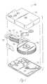
- FIG. 1is an exploded view of one type of a disc drive 100 having a rotary actuator with a micro actuator 180 .
- the disc drive 100includes a housing or base 112 , and a cover 114 .
- the base 112 and cover 114form a disc enclosure.
- Rotatably attached to the base 112 on an actuator shaft 118is an actuator assembly 120 .
- the actuator assembly 120includes a plurality of arms 123 . Attached to the separate arms 123 are load beams or load springs 124 .
- a microactuator 180is attached to the end of the separate arms and load beams 124 .
- a slider 126which carries a magnetic transducer 150 is attached at the end of microactuator 180 .
- a microactuator 180is one device that can be a MEMS device.
- FIG. 1illustrates a number of discs 134 within the disc drive, however the invention described herein is equally applicable to disc drives which have a plurality of discs as well as disc drives that have a single disc.
- the inventionis also useful in all types of disc drives including hard disc drives, zip drives, floppy disc drives and any other type of drive that utilizes MEMS devices. Any MEMS device may use the invention described herein.
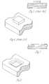
- FIG. 2is a section view illustrating a portion of a wafer 52 that may be used to fabricate a MEMS device 50 .
- FIG. 7is a section view similar to FIG. 2 illustrating the wafer 52 after it has been masked and then etched for use in a MEMS device 50 of the present invention.
- a surface 54 on the wafer 52is etched to form a pattern in the wafer 52 .
- the patterncomprises sidewalls 56 and an arcuate edge 60 .
- FIG. 8illustrates an embodiment of the MEMS device 50 where the pattern is in the form of a square opening that comprises four sidewalls 56 and an arcuate edge 60 .
- the arcuate edge 60 and the sidewalls 56are etched into the surface 54 of the wafer 52 such that the arcuate edge 56 is positioned between the each of the sidewalls 56 and the surface 54 of the wafer 52 .
- the arcuate edge 60extends around some, one or only a portion of the various sidewalls 56 without departing from the scope of the present invention.
- the arcuate edge formed as shownis a curved edge and so can be circular or elliptical or made of a portion of a circle or ellipse. It should also be noted that arcuate means other than straight or nearly straight and may include steps or slopes and still be within the scope of this invention.
- the patternis in the form of a round opening that comprises a single sidewall 61 and an arcuate edge 62 .
- the arcuate edge 62is etched between the entire sidewall 61 of the round opening and the surface 54 of the wafer 52 , although it should be noted that arcuate edge 62 may extend around only a portion of the sidewall 61 .
- FIG. 10illustrates the wafer 52 after it has been masked and then etched for use in another embodiment of the MEMS device 50 .
- the surface 54 on the wafer 52is etched to form a pattern that leaves an island 66 on a newly exposed surface 68 of the wafer 52 .
- the island 66comprises one or more side outer walls 70 having an arcuate edge 72 .
- the arcuate edge 72is an outside arcuate edge on the outside wall.
- the patternmay form a round island 66 on the exposed surface 68 of the wafer 52 .
- the round island 66comprises a single sidewall 70 and an arcuate edge 72 .
- the arcuate edge 72is etched between the entire sidewall 70 of the round opening and the original surface 54 of the wafer 52 , although it should be noted that arcuate edge 72 may extend around only a portion of the sidewall 70 .
- the patternmay also form a square island 76 on the wafer 52 .
- the square island 76comprises four sidewalls 78 and an arcuate edge 80 .
- the arcuate edge 80 and the sidewalls 78are etched into the surface 54 of the wafer 52 such that the arcuate edge 80 is positioned between the each of the sidewalls 78 and the original surface 54 of the wafer 52 .
- the arcuate edge 80extends around some, one or only a portion of the various sidewalls 78 .
- FIGS. 13 and 14illustrate another embodiment of the MEMS device 50 of the present invention.
- the MEMS device 50includes two layers.
- the two-layered MEMS device 50is formed by overlaying the wafer 52 with a layer 82 that is made from a different material.
- the surface 83 of the layer 82is etched to form a pattern in the layer 82 .
- the patternis etched downward from the surface 83 of the layer 82 until the surface 54 of the wafer 52 is exposed.
- the pattern illustrated in FIGS. 13 and 14is in the form of a rectangular opening that comprises four sidewalls 84 and an arcuate edge 85 .
- the arcuate edge 85 and the sidewalls 84are etched into the surface 83 of the wafer 82 such that the arcuate edge 85 is positioned between the each of the sidewalls 84 and the surface 83 of the layer 82 .
- FIGS. 15 and 16illustrate another embodiment of the MEMS device 50 that includes two layers.
- the surface 83 of the layer 82is etched with a pattern that forms an oval-shaped island 88 on the exposed surface 54 of the wafer 52 .
- the patterncomprises a single sidewall 89 and an arcuate edge 90 .
- the arcuate edge 90is etched between the entire sidewall 89 of the oval-shaped island 88 and the original surface 83 of the layer 82 .
- the MEMS device 50may include any number of layers without departing from the scope of the present invention.
- a MEMS device 50 having three layersis shown in FIG. 17.
- the wafer 52is covered with a first layer 82 (e.g. a conducting layer) and then a second layer 92 (e.g., an insulating layer).
- a surface 93 of the second layer 92is etched to form a pattern in the second layer 93 .
- the patterncomprises a sidewall 95 and an arcuate edge 96 .
- the patternis etched downward from the surface 93 of the second layer 92 until the surface 83 of the first layer 82 is exposed.
- the first layer 82may be further etched to expose the original surface 54 of the wafer 52 depending on the circuit design of the MEMS device 50 .
- the MEMs device 50 of the present inventioncould be masked using any method of masking that is now known or yet to be discovered.
- One form of a mask 200 that may be used to fabricate the arcuate edges in a MEMS device 50 of the present inventionis shown in FIG. 18.
- the mask 200is used to fabricate a pattern in a MEMS device 50 that is similar to the rectangular opening in the layer 82 of the MEMS device shown in FIG. 14.
- the mask 200includes a large center opening 204 . Passing light, or some other medium, through the center opening 204 in the mask 200 contributes to forming the sidewalls 84 in the pattern.
- the center opening 204is bordered by additional concentric openings 208 , 212 , 216 , 220 .
- the space between the openings 208 , 212 , 216 , 220increases as the openings 208 , 212 , 216 , 220 move outward toward an outside edge 224 of the photomask 200 . Therefore, more light passes through the photomask 200 near the center opening 204 than at the outside edge 224 . Passing this graduated dispersion of the light between the openings 208 , 212 , 216 , 220 contributes to similarly graduated etching that forms the arcuate edges 85 between the sidewalls 84 in the pattern and the surface 83 of the layer 82 on the MEMS device 50 .
- the size of the openings 208 , 212 , 216 , 220 in the mask 200may also be varied to facilitate etching the arcuate edges 85 in the pattern.
- Each opening 208 , 212 , 216 , 220would become increasingly smaller as the distance of each opening 208 , 212 , 216 , 220 from the center opening 204 increases.
- the MEMS device 50 of the present inventionmay also be etched using any etching method that is known or yet to be discovered.
- the etchingmay be wet or dry depending on the circuit design of the MEMS device 50 .
- the potential types of etchinginclude, but are not limited to; (i) immersing or spraying a liquid at the surface of the MEMS device 50 ; (ii) exposing the surface of the MEMS device 50 to a vapor or plasma; and/or (iii) directing an electron stream, x-rays or ions (reactive and non-reactive) at the surface of the MEMS device 50 .
- the MEMS device 50 describedis configured to facilitate engaging mating elements, such as actuators that are used in disc drives, with a pattern on the MEMS device 50 .
- the arcuate edges in all of disclosed embodiments of the MEMS devices 50minimize the fracturing of the MEMS devices 50 that typically occurs when a mating element is inserted on or into a MEMS device 50 .
- the etched patternforms an island (FIGS. 11, 12, 15 and 16 ) on the MEMS device 50 to facilitate handling the MEMS device 50 by the island
- the arcuate edgesreduce the amount of chipping and cracking that may be caused by handling the island with tweezers or any other type of handling device.
- the inventiondescribes the forming of a pattern on a MEMS device, it should be noted that the technique can be used to form such a pattern on any device including a slider for a disc drive or other device.
- the techniques and apparatus described hereinare not limited to only MEMS devices but can be used to form all devices.
- a method for topographically patterning a MEMS devicecomprises the steps of positioning a mask that is in the form of a pattern relative to the MEMS device and etching the pattern into a surface on the MEMS device 50 to form at least one sidewall and an arcuate edge between the surface and one of the sidewalls.
- the etching stepmay form an opening in the surface of MEMS device 50 or form an island on a newly exposed surface.
- the methodmay further comprise engaging a mating element with the pattern on the MEMS device 50 such that the arcuate edge formed during the etching step permits the mating element to be engaged with the pattern with little or no fracturing of the MEMS device 50 .
- the etching stepmay also comprise (i) immersing the MEMS device 50 ; (ii) spraying a liquid against the surface of the MEMS device 50 ; (iii) exposing the surface of the MEMS device 50 to a vapor or plasma; and (iv) directing an ion beam, stream of electrons and/or x-rays at the surface of the MEMS device 50 .
- the MEMS device 50may also comprise more than one layer such that the etching is done into one or more of the layers that make up the MEMS device 50 .
- a MEMS device 50that comprises a body having a surface, and a pattern etched into the body.
- the etched patterncomprises at least one sidewall and an arcuate edge that is positioned between the surface of the body and one of the sidewalls.
- the arcuate edgefacilitates engaging a mating element, such as an actuator, with the pattern.
- the bodymay also comprise two or more layers that are made from different materials with the pattern being etched into one or more of the layers.
- the inventiongenerally relates to a MEMS device that comprises a body having one or more layers.
- the bodycomprises means for engaging a mating element with one of the layers in the body.
- the means for engaging a mating element with one of the layers in the bodyminimizes any fracturing within the body that might occur when the mating element is engaged with the body.
Landscapes
- Engineering & Computer Science (AREA)
- Chemical & Material Sciences (AREA)
- Ceramic Engineering (AREA)
- Manufacturing & Machinery (AREA)
- Microelectronics & Electronic Packaging (AREA)
- Organic Chemistry (AREA)
- Materials Engineering (AREA)
- Structural Engineering (AREA)
- Physics & Mathematics (AREA)
- Geometry (AREA)
- Analytical Chemistry (AREA)
- General Physics & Mathematics (AREA)
- Condensed Matter Physics & Semiconductors (AREA)
- Computer Hardware Design (AREA)
- Power Engineering (AREA)
- Micromachines (AREA)
- Moving Of Heads (AREA)
- Supporting Of Heads In Record-Carrier Devices (AREA)
- Exposure And Positioning Against Photoresist Photosensitive Materials (AREA)
Abstract
Description
- This application claims the benefit of U.S. Provisional Application Serial No. 60/218,263, filed Jul. 13, 2000 under 35 U.S.C. 119(e).[0001]
- The present invention relates to the field of semiconductor devices and similar devices fabricated using masking and photolithography techniques. More particularly, this invention relates to fabricating a device that reduces internal stresses and prevents chipping or cracking when other elements are inserted therein or when handled.[0002]
- There are many classes of devices. One such class are MEMS (“micro electromechanical systems”) devices. MEMS devices are a class of systems that are physically small. These systems have both electrical and mechanical components. MEMS originally used modified integrated circuit (computer chip) fabrication techniques and materials to create these very small mechanical devices. Today there are many more fabrication techniques and materials available. One such fabrication technique includes sacrificial polysilicon surface micromachining which is a technology that enables the mass production of complex MEMS by themselves or MEMS integrated with microelectronic systems. This technology has already been successfully commercialized as acceleration sensors for automobile airbag deployment.[0003]
- There are many wide ranging application for MEMS devices. Two main categories of MEMS devices are sensors and actuators. Micro sensors are useful because their small physical size allows them to be much less invasive. Micro actuators are useful because the amount of work they perform is very precise. A polysilicon resonator transducer is an example of a MEMS sensor which uses stress controlled thin film polysilicon process to form a mechanically free beam of polysilicon having resonant frequency can be measured electronically. Environmental changes can be converted to a changes in resonant frequency of the micro beam. The environmental changes can be sensed.[0004]
- Other MEMS devices include magnetic micro motors fabricated by a deep x-ray lithography and electrode position process. The rotor is magnetically salient to allow a magnetic field applied to each of the two poles to cause the rotor to turn. External loading gears can be added. Gears are fabricated that are 100 microns tall. Techniques for forming MEMS devices can be used to create parts of systems where high tolerances are necessary which can bridge the gap between MEMS and traditionally machined precise components. MEMS are used to clean and treat semiconductor devices, low-voltage switches for radio frequency applications, micro-relay modules, spray nozzles for ink jet printers, and actuators for optical scanners, just to name a few. MEMS devices are becoming widely used in various industries. For example, in the automotive industry MEMS pressure sensors measure engine oil pressure, vacuum pressure, fuel injection pressure, transmission fluid pressure, various line pressures, tire pressure, and stored air bag pressures. MEMS temperature sensors can be used to monitor oil, antifreeze, and air temperatures. Other industries are also finding uses for MEMS devices. For example, in the disc drive industry MEMS devices are being contemplated to use as microactuators to very precisely position magnetic transducers over very closely packed tracks containing data.[0005]
- MEMS devices are typically fabricated by overlaying a semiconductor wafer made from silicon with layers of oxides, metals and other materials necessary for circuit construction. Patterns are formed on and within these layers in order to make a circuit plan of the device. The patterns usually include elements for two-dimensional and three-dimensional interactions of the MEMS device circuit plan.[0006]
- The patterns are formed in the MEMS device by a combination of masking and etching. Masking includes fabricating a mask that is in the form of a pattern and then positioning the mask on, or near, the surface of the MEMS device. The mask establishes how the MEMS device is to be etched. It is etching the MEMS device that permanently places the pattern into the MEMS device. Etching is typically done by removing the top layer(s) from the MEMS device in those areas that are either covered or uncovered by the mask depending on the type of etching that is used to remove the layer(s). Etching processes are either wet or dry, and the goal of any etching process is to transfer the desired pattern to the MEMS device.[0007]
- Semiconductors are another class of devices that are formed using photolithography, masking and etching. It is contemplated that other devices will also be formed using these techniques.[0008]
- One known masking method is photolithography which involves forming a pattern onto a photomask and then transferring the pattern to a radiation sensitive layer that has been placed on a semiconductor substrate. The radiation sensitive layer is typically called a photoresist layer. The pattern is transferred to the photoresist layer by exposing the photoresist to some form of light. The light extends through the mask to cross-link the photoresist in the form of the pattern. One of the exposed or unexposed portions of the photoresist is then subsequently removed from the substrate. The device is then etched, or not etched, in those areas of the substrate that are covered by the photoresist.[0009]
- FIG. 2 illustrates a portion of a wafer[0010]52 that is used in fabricating MEMS device50. FIGS.3-4 illustrate a similar wafer13 in a prior art MEMS device11 after the wafer13 has been has been masked and then etched to form a pattern in the wafer13. The square hole12 (i.e., pattern) extends downward into the surface16 of the wafer13 such the pattern is partially defined by sidewalls18. The etched pattern forms one or more “square” edges14 between the surface16 of the wafer13 and the sidewalls18 of the square opening12. When a mating element, such as an actuator in a disc drive, is inserted into the square opening12, the square edges14 have a tendency to chip and crack. This chipping and cracking of the edges14 generates debris that can negatively effect the operation of the MEMS device and other devices where the MEMS device is used.
- FIGS.[0011]5-6 illustrate another typical wafer19 that has been masked and etched to form a square island20 on the wafer19. The square island20 includes sidewalls28 that extend upward from an exposed surface25 of the wafer19. The island20 includes similar square edges22 between the original surface21 of the wafer19 and the sidewalls28 of the island20. These square edges22 are similarly vulnerable to chipping and cracking when a mating element is engaged with the island20. These square edges22 are also susceptible to damage when the island20 is grasped by a tweezers or some other handling device to maneuver the wafer19.
- Therefore, what is needed is a MEMS device that is configured to permit mating elements, such as actuators used in disc drives, to be inserted into the MEMS device without damaging the MEMS device. What is also needed is a method of fabricating a MEMS device that permits objects to be inserted into or on the MEMS device with minimal chipping and cracking of the MEMS device.[0012]
- The present invention relates to a method of fabricating a MEMS device. The method comprises positioning a mask that is in the form of a pattern relative to the MEMS device, and then etching the pattern into a surface on the MEMS device to form at least one sidewall and an arcuate edge such that the arcuate edge extends between the surface of the MEMS device and one of the sidewalls. The present invention can also be used on a slider of a disc drive to form arcuate or rounded edges.[0013]
- The present invention also relates to a MEMS device. The MEMS device comprises a body having a surface, and a pattern etched into the surface of the body. The pattern comprises at least one sidewall and an arcuate edge that extends between the surface of the body and one of the sidewalls.[0014]
- The MEMS device described is configured to facilitate engaging objects, such as actuators that are used in disc drives, with the pattern on the MEMS device. The arcuate edges between the sidewalls in the pattern and the surface of the MEMS device minimize some of the fracturing of the MEMS device that typically occurs when a mating element is inserted on or into the MEMS device. In addition, when the pattern on the MEMS device forms an island on the MEMS device to facilitate handling the MEMS device by the island, the arcuate edges reduce the amount of chipping and cracking fracturing that may be caused by handling the island with any type of handling device.[0015]
- The functioning of MEMS devices, and surrounding devices may be highly vulnerable to the contamination that results from the chipping and cracking generated when a mating element engages a MEMS device. Therefore, reducing the amount of chipping and cracking associated with engaging mating elements with MEM devices will produce MEMS devices with increased reliability and life expectancy. Forming such a device will also provide for increased reliability and life expectancy of devices in which these MEMs devices are used.[0016]
- The invention includes semiconductor structures, devices, and methods to form such structures and devices, of varying scope. In addition to the aspects and advantages of the present invention described in this summary, further aspects and advantages of the invention will become apparent by reference to the drawings and by reading the detailed description that follows.[0017]
- FIG. 1 is an exploded view of a disc drive with a multiple disc stack.[0018]
- FIG. 2 is a section view illustrating a portion of a typical wafer in a MEMS device.[0019]
- FIG. 3 is a section view similar to FIG. 2 illustrating a wafer in a prior art MEMS device after wafer has been etched to include a square opening.[0020]
- FIG. 4 is a perspective view of the wafer shown in FIG. 3.[0021]
- FIG. 5 is a section view similar to FIG. 2 illustrating a wafer in a prior art MEMS device after the wafer has been etched to include a square island.[0022]
- FIG. 6 is a perspective view of the wafer shown in FIG. 5.[0023]
- FIG. 7 is a section view illustrating a MEMS device of the present invention.[0024]
- FIG. 8 is a perspective view of the MEMS device shown in FIG. 7 with the MEMS device etched to include a square opening.[0025]
- FIG. 9 is a perspective view of the MEMS device shown in FIG. 7 with the MEMS device etched to include a round opening.[0026]
- FIG. 10 is a section view illustrating another embodiment of the MEMS device of the present invention.[0027]
- FIG. 11 is a perspective view of the MEMS device shown in FIG. 10 with the MEMS device etched to include a round island.[0028]
- FIG. 12 is a perspective view of the MEMS device shown in FIG. 10 with the MEMS device etched to include a square island.[0029]
- FIG. 13 is a section view illustrating a two-layered MEMS device of the present invention.[0030]
- FIG. 14 is a perspective view of the MEMS device shown in FIG. 13 with the upper layer of the MEMS device etched to include a rectangular opening.[0031]
- FIG. 15 is a section view illustrating another embodiment of a two-layered MEMS device of the present invention.[0032]
- FIG. 16 is a perspective view of the MEMS device shown in FIG. 15 with the upper layer of the MEMS device etched to include an oval-shaped island.[0033]
- FIG. 17 is a section view illustrating a three-layered MEMS device of the present invention.[0034]
- FIG. 18 is a plan view illustrating one form of a mask that could be used to fabricate the MEMS device shown in FIG. 9.[0035]
- In the following detailed description of the preferred embodiments, reference is made to the accompanying drawings which form a part hereof, and in which are shown by way of illustration specific embodiments in which the invention may be practiced. It is to be understood that other embodiments may be utilized and structural changes may be made without departing from the scope of the present invention.[0036]
- FIG. 1 is an exploded view of one type of a[0037]
disc drive 100 having a rotary actuator with amicro actuator 180. Thedisc drive 100 includes a housing orbase 112, and acover 114. Thebase 112 and cover114 form a disc enclosure. Rotatably attached to the base112 on anactuator shaft 118 is anactuator assembly 120. Theactuator assembly 120 includes a plurality ofarms 123. Attached to theseparate arms 123 are load beams or load springs124. Amicroactuator 180 is attached to the end of the separate arms and load beams124. Aslider 126 which carries amagnetic transducer 150 is attached at the end ofmicroactuator 180. Amicroactuator 180 is one device that can be a MEMS device. FIG. 1 illustrates a number ofdiscs 134 within the disc drive, however the invention described herein is equally applicable to disc drives which have a plurality of discs as well as disc drives that have a single disc. In addition, the invention is also useful in all types of disc drives including hard disc drives, zip drives, floppy disc drives and any other type of drive that utilizes MEMS devices. Any MEMS device may use the invention described herein. - FIG. 2 is a section view illustrating a portion of a wafer[0038]52 that may be used to fabricate a MEMS device50. FIG. 7 is a section view similar to FIG. 2 illustrating the wafer52 after it has been masked and then etched for use in a MEMS device50 of the present invention. A surface54 on the wafer52 is etched to form a pattern in the wafer52. The pattern comprises sidewalls56 and an arcuate edge60.
- FIG. 8 illustrates an embodiment of the MEMS device[0039]50 where the pattern is in the form of a square opening that comprises four sidewalls56 and an arcuate edge60. The arcuate edge60 and the sidewalls56 are etched into the surface54 of the wafer52 such that the arcuate edge56 is positioned between the each of the sidewalls56 and the surface54 of the wafer52. In an alternative form, the arcuate edge60 extends around some, one or only a portion of the various sidewalls56 without departing from the scope of the present invention. The arcuate edge formed as shown is a curved edge and so can be circular or elliptical or made of a portion of a circle or ellipse. It should also be noted that arcuate means other than straight or nearly straight and may include steps or slopes and still be within the scope of this invention.
- A similar embodiment is shown in FIG. 9. In this embodiment, the pattern is in the form of a round opening that comprises a single sidewall[0040]61 and an arcuate edge62. The arcuate edge62 is etched between the entire sidewall61 of the round opening and the surface54 of the wafer52, although it should be noted that arcuate edge62 may extend around only a portion of the sidewall61.
- FIG. 10 illustrates the wafer[0041]52 after it has been masked and then etched for use in another embodiment of the MEMS device50. The surface54 on the wafer52 is etched to form a pattern that leaves an island66 on a newly exposed surface68 of the wafer52. The island66 comprises one or more side outer walls70 having an arcuate edge72. The arcuate edge72 is an outside arcuate edge on the outside wall.
- Referring to FIG. 11, the pattern may form a round island[0042]66 on the exposed surface68 of the wafer52. The round island66 comprises a single sidewall70 and an arcuate edge72. The arcuate edge72 is etched between the entire sidewall70 of the round opening and the original surface54 of the wafer52, although it should be noted that arcuate edge72 may extend around only a portion of the sidewall70.
- As shown in FIG. 12, the pattern may also form a square island[0043]76 on the wafer52. The square island76 comprises four sidewalls78 and an arcuate edge80. The arcuate edge80 and the sidewalls78 are etched into the surface54 of the wafer52 such that the arcuate edge80 is positioned between the each of the sidewalls78 and the original surface54 of the wafer52. In an alternative form, the arcuate edge80 extends around some, one or only a portion of the various sidewalls78.
- FIGS. 13 and 14 illustrate another embodiment of the MEMS device[0044]50 of the present invention. In this embodiment, the MEMS device50 includes two layers. The two-layered MEMS device50 is formed by overlaying the wafer52 with a layer82 that is made from a different material. There are numerous layering techniques and types of layering materials that are well known to those skilled in the art. Any number of these techniques or materials may be used to form the layer82 on the wafer52 without departing from the scope of the present invention. The surface83 of the layer82 is etched to form a pattern in the layer82. The pattern is etched downward from the surface83 of the layer82 until the surface54 of the wafer52 is exposed. Although any other pattern could be etched into layer82, the pattern illustrated in FIGS. 13 and 14 is in the form of a rectangular opening that comprises four sidewalls84 and an arcuate edge85. The arcuate edge85 and the sidewalls84 are etched into the surface83 of the wafer82 such that the arcuate edge85 is positioned between the each of the sidewalls84 and the surface83 of the layer82.
- FIGS. 15 and 16 illustrate another embodiment of the MEMS device[0045]50 that includes two layers. In this embodiment, the surface83 of the layer82 is etched with a pattern that forms an oval-shaped island88 on the exposed surface54 of the wafer52. The pattern comprises a single sidewall89 and an arcuate edge90. The arcuate edge90 is etched between the entire sidewall89 of the oval-shaped island88 and the original surface83 of the layer82.
- The MEMS device[0046]50 may include any number of layers without departing from the scope of the present invention. A MEMS device50 having three layers is shown in FIG. 17. The wafer52 is covered with a first layer82 (e.g. a conducting layer) and then a second layer92 (e.g., an insulating layer). A surface93 of the second layer92 is etched to form a pattern in the second layer93. The pattern comprises a sidewall95 and an arcuate edge96. The pattern is etched downward from the surface93 of the second layer92 until the surface83 of the first layer82 is exposed. The first layer82 may be further etched to expose the original surface54 of the wafer52 depending on the circuit design of the MEMS device50.
- The MEMs device[0047]50 of the present invention could be masked using any method of masking that is now known or yet to be discovered. One form of a mask200 that may be used to fabricate the arcuate edges in a MEMS device50 of the present invention is shown in FIG. 18. The mask200 is used to fabricate a pattern in a MEMS device50 that is similar to the rectangular opening in the layer82 of the MEMS device shown in FIG. 14. The mask200 includes a large center opening204. Passing light, or some other medium, through the center opening204 in the mask200 contributes to forming the sidewalls84 in the pattern. The center opening204 is bordered by additional concentric openings208,212,216,220. The space between the openings208,212,216,220 increases as the openings208,212,216,220 move outward toward an outside edge224 of the photomask200. Therefore, more light passes through the photomask200 near the center opening204 than at the outside edge224. Passing this graduated dispersion of the light between the openings208,212,216,220 contributes to similarly graduated etching that forms the arcuate edges85 between the sidewalls84 in the pattern and the surface83 of the layer82 on the MEMS device50.
- The size of the openings[0048]208,212,216,220 in the mask200 may also be varied to facilitate etching the arcuate edges85 in the pattern. Each opening208,212,216,220 would become increasingly smaller as the distance of each opening208,212,216,220 from the center opening204 increases.
- The MEMS device[0049]50 of the present invention may also be etched using any etching method that is known or yet to be discovered. The etching may be wet or dry depending on the circuit design of the MEMS device50. The potential types of etching include, but are not limited to; (i) immersing or spraying a liquid at the surface of the MEMS device50; (ii) exposing the surface of the MEMS device50 to a vapor or plasma; and/or (iii) directing an electron stream, x-rays or ions (reactive and non-reactive) at the surface of the MEMS device50.
- The MEMS device[0050]50 described is configured to facilitate engaging mating elements, such as actuators that are used in disc drives, with a pattern on the MEMS device50. The arcuate edges in all of disclosed embodiments of the MEMS devices50 minimize the fracturing of the MEMS devices50 that typically occurs when a mating element is inserted on or into a MEMS device50. In addition, when the etched pattern forms an island (FIGS. 11, 12,15 and16) on the MEMS device50 to facilitate handling the MEMS device50 by the island, the arcuate edges reduce the amount of chipping and cracking that may be caused by handling the island with tweezers or any other type of handling device.
- Although the invention describes the forming of a pattern on a MEMS device, it should be noted that the technique can be used to form such a pattern on any device including a slider for a disc drive or other device. The techniques and apparatus described herein are not limited to only MEMS devices but can be used to form all devices.[0051]
- In conclusion, a method for topographically patterning a MEMS device is disclosed. The method comprises the steps of positioning a mask that is in the form of a pattern relative to the MEMS device and etching the pattern into a surface on the MEMS device[0052]50 to form at least one sidewall and an arcuate edge between the surface and one of the sidewalls. It should be noted that the etching step may form an opening in the surface of MEMS device50 or form an island on a newly exposed surface. The method may further comprise engaging a mating element with the pattern on the MEMS device50 such that the arcuate edge formed during the etching step permits the mating element to be engaged with the pattern with little or no fracturing of the MEMS device50. In addition, the arcuate edge may extend along all, some or a portion of any sidewall in the pattern. The etching step may also comprise (i) immersing the MEMS device50; (ii) spraying a liquid against the surface of the MEMS device50; (iii) exposing the surface of the MEMS device50 to a vapor or plasma; and (iv) directing an ion beam, stream of electrons and/or x-rays at the surface of the MEMS device50. The MEMS device50 may also comprise more than one layer such that the etching is done into one or more of the layers that make up the MEMS device50.
- Also disclosed is a MEMS device[0053]50 that comprises a body having a surface, and a pattern etched into the body. The etched pattern comprises at least one sidewall and an arcuate edge that is positioned between the surface of the body and one of the sidewalls. The arcuate edge facilitates engaging a mating element, such as an actuator, with the pattern. The body may also comprise two or more layers that are made from different materials with the pattern being etched into one or more of the layers.
- The invention generally relates to a MEMS device that comprises a body having one or more layers. The body comprises means for engaging a mating element with one of the layers in the body. The means for engaging a mating element with one of the layers in the body minimizes any fracturing within the body that might occur when the mating element is engaged with the body.[0054]
- It is to be understood that the above description is intended to be illustrative, and not restrictive. Many other embodiments will be apparent to those of skill in the art upon reviewing the above description. The scope of the invention should be determined with reference to the appended claims along with the full scope of equivalents to which such claims are entitled.[0055]
Claims (30)
Priority Applications (1)
| Application Number | Priority Date | Filing Date | Title |
|---|---|---|---|
| US09/905,037US7129179B2 (en) | 2000-07-13 | 2001-07-13 | Method for topographical patterning of a device |
Applications Claiming Priority (2)
| Application Number | Priority Date | Filing Date | Title |
|---|---|---|---|
| US21826300P | 2000-07-13 | 2000-07-13 | |
| US09/905,037US7129179B2 (en) | 2000-07-13 | 2001-07-13 | Method for topographical patterning of a device |
Publications (2)
| Publication Number | Publication Date |
|---|---|
| US20020135266A1true US20020135266A1 (en) | 2002-09-26 |
| US7129179B2 US7129179B2 (en) | 2006-10-31 |
Family
ID=22814411
Family Applications (1)
| Application Number | Title | Priority Date | Filing Date |
|---|---|---|---|
| US09/905,037Expired - Fee RelatedUS7129179B2 (en) | 2000-07-13 | 2001-07-13 | Method for topographical patterning of a device |
Country Status (6)
| Country | Link |
|---|---|
| US (1) | US7129179B2 (en) |
| JP (1) | JP2004508946A (en) |
| KR (1) | KR100532796B1 (en) |
| AU (1) | AU2002222920A1 (en) |
| GB (1) | GB2381383A (en) |
| WO (1) | WO2002006061A1 (en) |
Cited By (13)
| Publication number | Priority date | Publication date | Assignee | Title |
|---|---|---|---|---|
| US20030058418A1 (en)* | 1997-07-15 | 2003-03-27 | Kia Silverbrook | Photographic prints having magnetically recordable media |
| US20080284365A1 (en)* | 2003-04-11 | 2008-11-20 | International Business Machines Corporation | Servo system for a two-dimensional micro-electromechanical system (mems)-based scanner and method therefor |
| US8096642B2 (en) | 1997-08-11 | 2012-01-17 | Silverbrook Research Pty Ltd | Inkjet nozzle with paddle layer arranged between first and second wafers |
| US8102568B2 (en) | 1997-07-15 | 2012-01-24 | Silverbrook Research Pty Ltd | System for creating garments using camera and encoded card |
| US8274665B2 (en) | 1997-07-15 | 2012-09-25 | Silverbrook Research Pty Ltd | Image sensing and printing device |
| US8421869B2 (en) | 1997-07-15 | 2013-04-16 | Google Inc. | Camera system for with velocity sensor and de-blurring processor |
| US8789939B2 (en) | 1998-11-09 | 2014-07-29 | Google Inc. | Print media cartridge with ink supply manifold |
| US8823823B2 (en) | 1997-07-15 | 2014-09-02 | Google Inc. | Portable imaging device with multi-core processor and orientation sensor |
| US8866923B2 (en) | 1999-05-25 | 2014-10-21 | Google Inc. | Modular camera and printer |
| US8896724B2 (en) | 1997-07-15 | 2014-11-25 | Google Inc. | Camera system to facilitate a cascade of imaging effects |
| US8902333B2 (en) | 1997-07-15 | 2014-12-02 | Google Inc. | Image processing method using sensed eye position |
| US8908075B2 (en) | 1997-07-15 | 2014-12-09 | Google Inc. | Image capture and processing integrated circuit for a camera |
| US8936196B2 (en) | 1997-07-15 | 2015-01-20 | Google Inc. | Camera unit incorporating program script scanner |
Citations (25)
| Publication number | Priority date | Publication date | Assignee | Title |
|---|---|---|---|---|
| US4035062A (en)* | 1975-12-30 | 1977-07-12 | Nasa | Method and apparatus for producing an image from a transparent object |
| US4567104A (en)* | 1983-06-24 | 1986-01-28 | Canyon Materials Research & Engineering | High energy beam colored glasses exhibiting insensitivity to actinic radiation |
| US4670336A (en)* | 1984-08-11 | 1987-06-02 | Bayer Aktiengesellschaft | Laundry-stable, antimicrobially-active fibers and filaments and the production thereof |
| US4894303A (en)* | 1983-06-24 | 1990-01-16 | Canyon Materials Research & Engineering | High energy beam-sensitive glasses |
| US5078771A (en)* | 1989-02-07 | 1992-01-07 | Canyon Materials, Inc. | Method of making high energy beam sensitive glasses |
| US5079130A (en)* | 1990-05-25 | 1992-01-07 | At&T Bell Laboratories | Partially or fully recessed microlens fabrication |
| US5114813A (en)* | 1989-06-23 | 1992-05-19 | Schott Glass Technologies, Inc. | Method of forming stable images in electron beam writable glass compositions |
| US5126006A (en)* | 1990-10-30 | 1992-06-30 | International Business Machines Corp. | Plural level chip masking |
| US5145757A (en)* | 1989-06-23 | 1992-09-08 | Schott Glass Technologies, Inc. | Method of forming stable images in electron beam writable glass compositions |
| US5192699A (en)* | 1990-12-17 | 1993-03-09 | Gte Laboratories Incorporated | Method of fabricating field effect transistors |
| US5213916A (en)* | 1990-10-30 | 1993-05-25 | International Business Machines Corporation | Method of making a gray level mask |
| US5242707A (en)* | 1990-12-21 | 1993-09-07 | Regents Of The University Of California | System and method for producing electro-optic components integrable with silicon-on-sapphire circuits |
| US5285517A (en)* | 1983-06-24 | 1994-02-08 | Canyon Materials, Inc. | High energy beam sensitive glasses |
| US5285438A (en)* | 1991-10-31 | 1994-02-08 | Regents Of The University Of California | Motionless parallel readout head for an optical disk recorded with arrayed one-dimensional holograms |
| US5310623A (en)* | 1992-11-27 | 1994-05-10 | Lockheed Missiles & Space Company, Inc. | Method for fabricating microlenses |
| US5316640A (en)* | 1991-06-19 | 1994-05-31 | Matsushita Electric Industrial Co., Ltd. | Fabricating method of micro lens |
| US5456798A (en)* | 1993-04-16 | 1995-10-10 | Nippondenso Co., Ltd. | Methods and apparatus for processing curved surface |
| US5508803A (en)* | 1994-12-20 | 1996-04-16 | International Business Machines Corporation | Method and apparatus for monitoring lithographic exposure |
| US5521781A (en)* | 1992-10-30 | 1996-05-28 | Shin-Etsu Chemical Co., Ltd. | Substrate for magnetic recording medium |
| US5538817A (en)* | 1994-06-17 | 1996-07-23 | Litel Instruments | Gray level imaging masks and methods for encoding same |
| US5804084A (en)* | 1996-10-11 | 1998-09-08 | Sandia Corporation | Use of chemical mechanical polishing in micromachining |
| US5853959A (en)* | 1996-08-09 | 1998-12-29 | Seagate Technology, Inc. | Method of fabricating a contoured slider surface feature with a single mask |
| US6107000A (en)* | 1996-12-17 | 2000-08-22 | Board Of Regents - University Of California - San Diego | Method for producing micro-optic elements with gray scale mask |
| US6335224B1 (en)* | 2000-05-16 | 2002-01-01 | Sandia Corporation | Protection of microelectronic devices during packaging |
| US6344383B1 (en)* | 1998-10-15 | 2002-02-05 | International Business Machines Corporation | Structure and method for dual gate oxidation for CMOS technology |
Family Cites Families (3)
| Publication number | Priority date | Publication date | Assignee | Title |
|---|---|---|---|---|
| US4670366A (en) | 1983-06-24 | 1987-06-02 | Canyon Materials Research & Engineering | High energy beam sensitive glasses |
| US4719498A (en)* | 1984-05-18 | 1988-01-12 | Fujitsu Limited | Optoelectronic integrated circuit |
| US4581814A (en)* | 1984-12-13 | 1986-04-15 | At&T Bell Laboratories | Process for fabricating dielectrically isolated devices utilizing heating of the polycrystalline support layer to prevent substrate deformation |
- 2001
- 2001-07-13GBGB0301024Apatent/GB2381383A/ennot_activeWithdrawn
- 2001-07-13AUAU2002222920Apatent/AU2002222920A1/ennot_activeAbandoned
- 2001-07-13USUS09/905,037patent/US7129179B2/ennot_activeExpired - Fee Related
- 2001-07-13WOPCT/US2001/022037patent/WO2002006061A1/enactiveIP Right Grant
- 2001-07-13JPJP2002511978Apatent/JP2004508946A/enactivePending
- 2001-07-13KRKR10-2003-7000506Apatent/KR100532796B1/ennot_activeExpired - Fee Related
Patent Citations (27)
| Publication number | Priority date | Publication date | Assignee | Title |
|---|---|---|---|---|
| US4035062A (en)* | 1975-12-30 | 1977-07-12 | Nasa | Method and apparatus for producing an image from a transparent object |
| US4567104A (en)* | 1983-06-24 | 1986-01-28 | Canyon Materials Research & Engineering | High energy beam colored glasses exhibiting insensitivity to actinic radiation |
| US4894303A (en)* | 1983-06-24 | 1990-01-16 | Canyon Materials Research & Engineering | High energy beam-sensitive glasses |
| US5285517A (en)* | 1983-06-24 | 1994-02-08 | Canyon Materials, Inc. | High energy beam sensitive glasses |
| US4670336A (en)* | 1984-08-11 | 1987-06-02 | Bayer Aktiengesellschaft | Laundry-stable, antimicrobially-active fibers and filaments and the production thereof |
| US5078771A (en)* | 1989-02-07 | 1992-01-07 | Canyon Materials, Inc. | Method of making high energy beam sensitive glasses |
| US5114813A (en)* | 1989-06-23 | 1992-05-19 | Schott Glass Technologies, Inc. | Method of forming stable images in electron beam writable glass compositions |
| US5145757A (en)* | 1989-06-23 | 1992-09-08 | Schott Glass Technologies, Inc. | Method of forming stable images in electron beam writable glass compositions |
| US5079130A (en)* | 1990-05-25 | 1992-01-07 | At&T Bell Laboratories | Partially or fully recessed microlens fabrication |
| US5213916A (en)* | 1990-10-30 | 1993-05-25 | International Business Machines Corporation | Method of making a gray level mask |
| US5334467A (en)* | 1990-10-30 | 1994-08-02 | International Business Machines Corporation | Gray level mask |
| US5126006A (en)* | 1990-10-30 | 1992-06-30 | International Business Machines Corp. | Plural level chip masking |
| US5192699A (en)* | 1990-12-17 | 1993-03-09 | Gte Laboratories Incorporated | Method of fabricating field effect transistors |
| US5242707A (en)* | 1990-12-21 | 1993-09-07 | Regents Of The University Of California | System and method for producing electro-optic components integrable with silicon-on-sapphire circuits |
| US5316640A (en)* | 1991-06-19 | 1994-05-31 | Matsushita Electric Industrial Co., Ltd. | Fabricating method of micro lens |
| US5285438A (en)* | 1991-10-31 | 1994-02-08 | Regents Of The University Of California | Motionless parallel readout head for an optical disk recorded with arrayed one-dimensional holograms |
| US5521781A (en)* | 1992-10-30 | 1996-05-28 | Shin-Etsu Chemical Co., Ltd. | Substrate for magnetic recording medium |
| US5310623A (en)* | 1992-11-27 | 1994-05-10 | Lockheed Missiles & Space Company, Inc. | Method for fabricating microlenses |
| US5480764A (en)* | 1992-11-27 | 1996-01-02 | Lockheed Missiles And Space Comapny, Inc. | Gray scale microfabrication for integrated optical devices |
| US5456798A (en)* | 1993-04-16 | 1995-10-10 | Nippondenso Co., Ltd. | Methods and apparatus for processing curved surface |
| US5538817A (en)* | 1994-06-17 | 1996-07-23 | Litel Instruments | Gray level imaging masks and methods for encoding same |
| US5508803A (en)* | 1994-12-20 | 1996-04-16 | International Business Machines Corporation | Method and apparatus for monitoring lithographic exposure |
| US5853959A (en)* | 1996-08-09 | 1998-12-29 | Seagate Technology, Inc. | Method of fabricating a contoured slider surface feature with a single mask |
| US5804084A (en)* | 1996-10-11 | 1998-09-08 | Sandia Corporation | Use of chemical mechanical polishing in micromachining |
| US6107000A (en)* | 1996-12-17 | 2000-08-22 | Board Of Regents - University Of California - San Diego | Method for producing micro-optic elements with gray scale mask |
| US6344383B1 (en)* | 1998-10-15 | 2002-02-05 | International Business Machines Corporation | Structure and method for dual gate oxidation for CMOS technology |
| US6335224B1 (en)* | 2000-05-16 | 2002-01-01 | Sandia Corporation | Protection of microelectronic devices during packaging |
Cited By (69)
| Publication number | Priority date | Publication date | Assignee | Title |
|---|---|---|---|---|
| US8902340B2 (en) | 1997-07-12 | 2014-12-02 | Google Inc. | Multi-core image processor for portable device |
| US9544451B2 (en) | 1997-07-12 | 2017-01-10 | Google Inc. | Multi-core image processor for portable device |
| US9338312B2 (en) | 1997-07-12 | 2016-05-10 | Google Inc. | Portable handheld device with multi-core image processor |
| US8947592B2 (en) | 1997-07-12 | 2015-02-03 | Google Inc. | Handheld imaging device with image processor provided with multiple parallel processing units |
| US8922791B2 (en) | 1997-07-15 | 2014-12-30 | Google Inc. | Camera system with color display and processor for Reed-Solomon decoding |
| US8934027B2 (en) | 1997-07-15 | 2015-01-13 | Google Inc. | Portable device with image sensors and multi-core processor |
| US7590347B2 (en) | 1997-07-15 | 2009-09-15 | Silverbrook Research Pty Ltd | Photographic prints having magnetically recordable media |
| US20090304376A1 (en)* | 1997-07-15 | 2009-12-10 | Silverbrook Research Pty Ltd | Digital Camera Having Printhead And Magnetic Recorder |
| US7742696B2 (en) | 1997-07-15 | 2010-06-22 | Silverbrook Research Pty Ltd | Digital camera having printhead and magnetic recorder |
| US20100254694A1 (en)* | 1997-07-15 | 2010-10-07 | Silverbrook Research Pty Ltd | Digital camera system for simultaneous printing and magnetic recording |
| US7970275B2 (en) | 1997-07-15 | 2011-06-28 | Silverbrook Research Pty Ltd | Digital camera system for simultaneous printing and magnetic recording |
| US9584681B2 (en) | 1997-07-15 | 2017-02-28 | Google Inc. | Handheld imaging device incorporating multi-core image processor |
| US8102568B2 (en) | 1997-07-15 | 2012-01-24 | Silverbrook Research Pty Ltd | System for creating garments using camera and encoded card |
| US8274665B2 (en) | 1997-07-15 | 2012-09-25 | Silverbrook Research Pty Ltd | Image sensing and printing device |
| US8285137B2 (en) | 1997-07-15 | 2012-10-09 | Silverbrook Research Pty Ltd | Digital camera system for simultaneous printing and magnetic recording |
| US8421869B2 (en) | 1997-07-15 | 2013-04-16 | Google Inc. | Camera system for with velocity sensor and de-blurring processor |
| US9560221B2 (en) | 1997-07-15 | 2017-01-31 | Google Inc. | Handheld imaging device with VLIW image processor |
| US8823823B2 (en) | 1997-07-15 | 2014-09-02 | Google Inc. | Portable imaging device with multi-core processor and orientation sensor |
| US8836809B2 (en) | 1997-07-15 | 2014-09-16 | Google Inc. | Quad-core image processor for facial detection |
| US6985207B2 (en)* | 1997-07-15 | 2006-01-10 | Silverbrook Research Pty Ltd | Photographic prints having magnetically recordable media |
| US8866926B2 (en) | 1997-07-15 | 2014-10-21 | Google Inc. | Multi-core processor for hand-held, image capture device |
| US8896720B2 (en) | 1997-07-15 | 2014-11-25 | Google Inc. | Hand held image capture device with multi-core processor for facial detection |
| US8896724B2 (en) | 1997-07-15 | 2014-11-25 | Google Inc. | Camera system to facilitate a cascade of imaging effects |
| US8902333B2 (en) | 1997-07-15 | 2014-12-02 | Google Inc. | Image processing method using sensed eye position |
| US8902357B2 (en) | 1997-07-15 | 2014-12-02 | Google Inc. | Quad-core image processor |
| US7558476B2 (en) | 1997-07-15 | 2009-07-07 | Silverbrook Research Pty Ltd | Digital camera with ancillary data capture |
| US8902324B2 (en) | 1997-07-15 | 2014-12-02 | Google Inc. | Quad-core image processor for device with image display |
| US8908069B2 (en) | 1997-07-15 | 2014-12-09 | Google Inc. | Handheld imaging device with quad-core image processor integrating image sensor interface |
| US8908075B2 (en) | 1997-07-15 | 2014-12-09 | Google Inc. | Image capture and processing integrated circuit for a camera |
| US8908051B2 (en) | 1997-07-15 | 2014-12-09 | Google Inc. | Handheld imaging device with system-on-chip microcontroller incorporating on shared wafer image processor and image sensor |
| US8913151B2 (en) | 1997-07-15 | 2014-12-16 | Google Inc. | Digital camera with quad core processor |
| US8913137B2 (en) | 1997-07-15 | 2014-12-16 | Google Inc. | Handheld imaging device with multi-core image processor integrating image sensor interface |
| US8913182B2 (en) | 1997-07-15 | 2014-12-16 | Google Inc. | Portable hand-held device having networked quad core processor |
| US8922670B2 (en) | 1997-07-15 | 2014-12-30 | Google Inc. | Portable hand-held device having stereoscopic image camera |
| US20030058418A1 (en)* | 1997-07-15 | 2003-03-27 | Kia Silverbrook | Photographic prints having magnetically recordable media |
| US8928897B2 (en) | 1997-07-15 | 2015-01-06 | Google Inc. | Portable handheld device with multi-core image processor |
| US9432529B2 (en) | 1997-07-15 | 2016-08-30 | Google Inc. | Portable handheld device with multi-core microcoded image processor |
| US8934053B2 (en) | 1997-07-15 | 2015-01-13 | Google Inc. | Hand-held quad core processing apparatus |
| US8936196B2 (en) | 1997-07-15 | 2015-01-20 | Google Inc. | Camera unit incorporating program script scanner |
| US8937727B2 (en) | 1997-07-15 | 2015-01-20 | Google Inc. | Portable handheld device with multi-core image processor |
| US20080075443A1 (en)* | 1997-07-15 | 2008-03-27 | Silverbrook Research Pty Ltd | Photographic Prints Having Magnetically Recordable Media |
| US8947679B2 (en) | 1997-07-15 | 2015-02-03 | Google Inc. | Portable handheld device with multi-core microcoded image processor |
| US8953060B2 (en) | 1997-07-15 | 2015-02-10 | Google Inc. | Hand held image capture device with multi-core processor and wireless interface to input device |
| US8953061B2 (en) | 1997-07-15 | 2015-02-10 | Google Inc. | Image capture device with linked multi-core processor and orientation sensor |
| US8953178B2 (en) | 1997-07-15 | 2015-02-10 | Google Inc. | Camera system with color display and processor for reed-solomon decoding |
| US9055221B2 (en) | 1997-07-15 | 2015-06-09 | Google Inc. | Portable hand-held device for deblurring sensed images |
| US9060128B2 (en) | 1997-07-15 | 2015-06-16 | Google Inc. | Portable hand-held device for manipulating images |
| US9124736B2 (en) | 1997-07-15 | 2015-09-01 | Google Inc. | Portable hand-held device for displaying oriented images |
| US9124737B2 (en) | 1997-07-15 | 2015-09-01 | Google Inc. | Portable device with image sensor and quad-core processor for multi-point focus image capture |
| US9131083B2 (en) | 1997-07-15 | 2015-09-08 | Google Inc. | Portable imaging device with multi-core processor |
| US9137398B2 (en) | 1997-07-15 | 2015-09-15 | Google Inc. | Multi-core processor for portable device with dual image sensors |
| US9137397B2 (en) | 1997-07-15 | 2015-09-15 | Google Inc. | Image sensing and printing device |
| US9143635B2 (en) | 1997-07-15 | 2015-09-22 | Google Inc. | Camera with linked parallel processor cores |
| US9143636B2 (en) | 1997-07-15 | 2015-09-22 | Google Inc. | Portable device with dual image sensors and quad-core processor |
| US9148530B2 (en) | 1997-07-15 | 2015-09-29 | Google Inc. | Handheld imaging device with multi-core image processor integrating common bus interface and dedicated image sensor interface |
| US9168761B2 (en) | 1997-07-15 | 2015-10-27 | Google Inc. | Disposable digital camera with printing assembly |
| US9179020B2 (en) | 1997-07-15 | 2015-11-03 | Google Inc. | Handheld imaging device with integrated chip incorporating on shared wafer image processor and central processor |
| US9185247B2 (en) | 1997-07-15 | 2015-11-10 | Google Inc. | Central processor with multiple programmable processor units |
| US9185246B2 (en) | 1997-07-15 | 2015-11-10 | Google Inc. | Camera system comprising color display and processor for decoding data blocks in printed coding pattern |
| US9191530B2 (en) | 1997-07-15 | 2015-11-17 | Google Inc. | Portable hand-held device having quad core image processor |
| US9191529B2 (en) | 1997-07-15 | 2015-11-17 | Google Inc | Quad-core camera processor |
| US9197767B2 (en) | 1997-07-15 | 2015-11-24 | Google Inc. | Digital camera having image processor and printer |
| US9219832B2 (en) | 1997-07-15 | 2015-12-22 | Google Inc. | Portable handheld device with multi-core image processor |
| US9237244B2 (en) | 1997-07-15 | 2016-01-12 | Google Inc. | Handheld digital camera device with orientation sensing and decoding capabilities |
| US8096642B2 (en) | 1997-08-11 | 2012-01-17 | Silverbrook Research Pty Ltd | Inkjet nozzle with paddle layer arranged between first and second wafers |
| US8789939B2 (en) | 1998-11-09 | 2014-07-29 | Google Inc. | Print media cartridge with ink supply manifold |
| US8866923B2 (en) | 1999-05-25 | 2014-10-21 | Google Inc. | Modular camera and printer |
| US20080284365A1 (en)* | 2003-04-11 | 2008-11-20 | International Business Machines Corporation | Servo system for a two-dimensional micro-electromechanical system (mems)-based scanner and method therefor |
| US7583044B2 (en)* | 2003-04-11 | 2009-09-01 | International Business Machines Corporation | Servo system for a two-dimensional micro-electromechanical system (MEMS)-based scanner and method therefor |
Also Published As
| Publication number | Publication date |
|---|---|
| GB0301024D0 (en) | 2003-02-19 |
| KR100532796B1 (en) | 2005-12-02 |
| GB2381383A (en) | 2003-04-30 |
| AU2002222920A1 (en) | 2002-01-30 |
| US7129179B2 (en) | 2006-10-31 |
| JP2004508946A (en) | 2004-03-25 |
| WO2002006061A1 (en) | 2002-01-24 |
| KR20030019573A (en) | 2003-03-06 |
Similar Documents
| Publication | Publication Date | Title |
|---|---|---|
| US7129179B2 (en) | Method for topographical patterning of a device | |
| US7145213B1 (en) | MEMS RF switch integrated process | |
| US7381583B1 (en) | MEMS RF switch integrated process | |
| US6878638B2 (en) | Multi-level integrated circuit for wide-gap substrate bonding | |
| KR100421217B1 (en) | Method for fabricating stiction-resistant micromachined structures | |
| US5364497A (en) | Method for fabricating microstructures using temporary bridges | |
| US6872319B2 (en) | Process for high yield fabrication of MEMS devices | |
| US11952266B2 (en) | Micro-device structures with etch holes | |
| JP4544880B2 (en) | Method for sealing micro electromechanical device | |
| EP0435237A1 (en) | Electrostatic miniature valve and method for its fabrication | |
| EP1101730A2 (en) | Encapsulation process for microelectromechanical structures | |
| US20030038327A1 (en) | Hermetically sealed silicon micro-machined electromechanical system (MEMS) device having diffused conductors | |
| JPH07505743A (en) | How to make microstructures | |
| US20070181979A1 (en) | Microelectromechanical semiconductor component with cavity structure and method for producing the same | |
| EP0683921A1 (en) | Microstructures and single mask, single-crystal process for fabrication thereof | |
| JP2006147995A (en) | Variable capacitance element and manufacturing method thereof | |
| TWI614816B (en) | Method of etching and singulating a cap wafer | |
| US12006205B2 (en) | Micro-device structures with etch holes | |
| US20110012214A1 (en) | Microelectromechanical semiconductor component with cavity structure and method for producing the same | |
| US6242363B1 (en) | Method of etching a wafer layer using a sacrificial wall to form vertical sidewall | |
| KR100691046B1 (en) | Electrode patterning for differential PPT activators | |
| US6544863B1 (en) | Method of fabricating semiconductor wafers having multiple height subsurface layers | |
| US6953704B2 (en) | Systems with high density packing of micromachines | |
| US7234237B2 (en) | Method for producing a protective cover for a device | |
| US11130671B2 (en) | MEMS device and fabrication method thereof |
Legal Events
| Date | Code | Title | Description |
|---|---|---|---|
| AS | Assignment | Owner name:SEAGATE TECHNOLOGY LLC, CALIFORNIA Free format text:ASSIGNMENT OF ASSIGNORS INTEREST;ASSIGNOR:BOUTAGHOU, ZINE EDDINE;REEL/FRAME:012588/0680 Effective date:20010918 | |
| AS | Assignment | Owner name:JPMORGAN CHASE BANK, AS COLLATERAL AGENT, NEW YORK Free format text:SECURITY AGREEMENT;ASSIGNOR:SEAGATE TECHNOLOGY LLC;REEL/FRAME:013177/0001 Effective date:20020513 Owner name:JPMORGAN CHASE BANK, AS COLLATERAL AGENT,NEW YORK Free format text:SECURITY AGREEMENT;ASSIGNOR:SEAGATE TECHNOLOGY LLC;REEL/FRAME:013177/0001 Effective date:20020513 | |
| AS | Assignment | Owner name:SEAGATE TECHNOLOGY LLC,CALIFORNIA Free format text:RELEASE OF SECURITY INTERESTS IN PATENT RIGHTS;ASSIGNOR:JPMORGAN CHASE BANK, N.A., AS ADMINISTRATIVE AGENT (FORMERLY KNOWN AS THE CHASE MANHATTAN BANK AND JPMORGAN CHASE BANK);REEL/FRAME:016926/0342 Effective date:20051130 Owner name:SEAGATE TECHNOLOGY LLC, CALIFORNIA Free format text:RELEASE OF SECURITY INTERESTS IN PATENT RIGHTS;ASSIGNOR:JPMORGAN CHASE BANK, N.A., AS ADMINISTRATIVE AGENT (FORMERLY KNOWN AS THE CHASE MANHATTAN BANK AND JPMORGAN CHASE BANK);REEL/FRAME:016926/0342 Effective date:20051130 | |
| AS | Assignment | Owner name:WELLS FARGO BANK, NATIONAL ASSOCIATION, AS COLLATERAL AGENT AND SECOND PRIORITY REPRESENTATIVE, CALIFORNIA Free format text:SECURITY AGREEMENT;ASSIGNORS:MAXTOR CORPORATION;SEAGATE TECHNOLOGY LLC;SEAGATE TECHNOLOGY INTERNATIONAL;REEL/FRAME:022757/0017 Effective date:20090507 Owner name:JPMORGAN CHASE BANK, N.A., AS ADMINISTRATIVE AGENT AND FIRST PRIORITY REPRESENTATIVE, NEW YORK Free format text:SECURITY AGREEMENT;ASSIGNORS:MAXTOR CORPORATION;SEAGATE TECHNOLOGY LLC;SEAGATE TECHNOLOGY INTERNATIONAL;REEL/FRAME:022757/0017 Effective date:20090507 Owner name:JPMORGAN CHASE BANK, N.A., AS ADMINISTRATIVE AGENT Free format text:SECURITY AGREEMENT;ASSIGNORS:MAXTOR CORPORATION;SEAGATE TECHNOLOGY LLC;SEAGATE TECHNOLOGY INTERNATIONAL;REEL/FRAME:022757/0017 Effective date:20090507 Owner name:WELLS FARGO BANK, NATIONAL ASSOCIATION, AS COLLATE Free format text:SECURITY AGREEMENT;ASSIGNORS:MAXTOR CORPORATION;SEAGATE TECHNOLOGY LLC;SEAGATE TECHNOLOGY INTERNATIONAL;REEL/FRAME:022757/0017 Effective date:20090507 | |
| REMI | Maintenance fee reminder mailed | ||
| LAPS | Lapse for failure to pay maintenance fees | ||
| STCH | Information on status: patent discontinuation | Free format text:PATENT EXPIRED DUE TO NONPAYMENT OF MAINTENANCE FEES UNDER 37 CFR 1.362 | |
| FP | Lapsed due to failure to pay maintenance fee | Effective date:20101031 | |
| AS | Assignment | Owner name:SEAGATE TECHNOLOGY INTERNATIONAL, CALIFORNIA Free format text:RELEASE;ASSIGNOR:JPMORGAN CHASE BANK, N.A., AS ADMINISTRATIVE AGENT;REEL/FRAME:025662/0001 Effective date:20110114 Owner name:SEAGATE TECHNOLOGY HDD HOLDINGS, CALIFORNIA Free format text:RELEASE;ASSIGNOR:JPMORGAN CHASE BANK, N.A., AS ADMINISTRATIVE AGENT;REEL/FRAME:025662/0001 Effective date:20110114 Owner name:SEAGATE TECHNOLOGY LLC, CALIFORNIA Free format text:RELEASE;ASSIGNOR:JPMORGAN CHASE BANK, N.A., AS ADMINISTRATIVE AGENT;REEL/FRAME:025662/0001 Effective date:20110114 Owner name:MAXTOR CORPORATION, CALIFORNIA Free format text:RELEASE;ASSIGNOR:JPMORGAN CHASE BANK, N.A., AS ADMINISTRATIVE AGENT;REEL/FRAME:025662/0001 Effective date:20110114 | |
| AS | Assignment | Owner name:SEAGATE TECHNOLOGY INTERNATIONAL, CAYMAN ISLANDS Free format text:TERMINATION AND RELEASE OF SECURITY INTEREST IN PATENT RIGHTS;ASSIGNOR:WELLS FARGO BANK, NATIONAL ASSOCIATION, AS COLLATERAL AGENT AND SECOND PRIORITY REPRESENTATIVE;REEL/FRAME:030833/0001 Effective date:20130312 Owner name:EVAULT INC. (F/K/A I365 INC.), CALIFORNIA Free format text:TERMINATION AND RELEASE OF SECURITY INTEREST IN PATENT RIGHTS;ASSIGNOR:WELLS FARGO BANK, NATIONAL ASSOCIATION, AS COLLATERAL AGENT AND SECOND PRIORITY REPRESENTATIVE;REEL/FRAME:030833/0001 Effective date:20130312 Owner name:SEAGATE TECHNOLOGY LLC, CALIFORNIA Free format text:TERMINATION AND RELEASE OF SECURITY INTEREST IN PATENT RIGHTS;ASSIGNOR:WELLS FARGO BANK, NATIONAL ASSOCIATION, AS COLLATERAL AGENT AND SECOND PRIORITY REPRESENTATIVE;REEL/FRAME:030833/0001 Effective date:20130312 Owner name:SEAGATE TECHNOLOGY US HOLDINGS, INC., CALIFORNIA Free format text:TERMINATION AND RELEASE OF SECURITY INTEREST IN PATENT RIGHTS;ASSIGNOR:WELLS FARGO BANK, NATIONAL ASSOCIATION, AS COLLATERAL AGENT AND SECOND PRIORITY REPRESENTATIVE;REEL/FRAME:030833/0001 Effective date:20130312 |