US20020134582A1 - Integrated circuit package and method - Google Patents
Integrated circuit package and methodDownload PDFInfo
- Publication number
- US20020134582A1 US20020134582A1US09/817,330US81733001AUS2002134582A1US 20020134582 A1US20020134582 A1US 20020134582A1US 81733001 AUS81733001 AUS 81733001AUS 2002134582 A1US2002134582 A1US 2002134582A1
- Authority
- US
- United States
- Prior art keywords
- integrated circuit
- conductive material
- lead
- substrate
- semiconductor die
- Prior art date
- Legal status (The legal status is an assumption and is not a legal conclusion. Google has not performed a legal analysis and makes no representation as to the accuracy of the status listed.)
- Granted
Links
- 238000000034methodMethods0.000titleclaimsdescription28
- 239000000758substrateSubstances0.000claimsabstractdescription36
- 239000004020conductorSubstances0.000claimsabstractdescription34
- 239000004065semiconductorSubstances0.000claimsabstractdescription29
- 238000007747platingMethods0.000claimsabstractdescription22
- 230000008878couplingEffects0.000claimsabstractdescription9
- 238000010168coupling processMethods0.000claimsabstractdescription9
- 238000005859coupling reactionMethods0.000claimsabstractdescription9
- RYGMFSIKBFXOCR-UHFFFAOYSA-NCopperChemical compound[Cu]RYGMFSIKBFXOCR-UHFFFAOYSA-N0.000claimsdescription25
- 229910000679solderInorganic materials0.000claimsdescription25
- 229910052802copperInorganic materials0.000claimsdescription19
- 239000010949copperSubstances0.000claimsdescription19
- 229920002120photoresistant polymerPolymers0.000claimsdescription11
- 239000000463materialSubstances0.000claimsdescription9
- 238000004519manufacturing processMethods0.000claimsdescription8
- 239000003989dielectric materialSubstances0.000claimsdescription4
- 239000011347resinSubstances0.000claimsdescription2
- 229920005989resinPolymers0.000claimsdescription2
- 238000000059patterningMethods0.000claims2
- 239000012212insulatorSubstances0.000claims1
- 239000011889copper foilSubstances0.000description6
- 239000004593EpoxySubstances0.000description3
- 230000007613environmental effectEffects0.000description3
- 230000000873masking effectEffects0.000description3
- 239000011888foilSubstances0.000description2
- 239000011521glassSubstances0.000description2
- GCTFTMWXZFLTRR-GFCCVEGCSA-N(2r)-2-amino-n-[3-(difluoromethoxy)-4-(1,3-oxazol-5-yl)phenyl]-4-methylpentanamideChemical compoundFC(F)OC1=CC(NC(=O)[C@H](N)CC(C)C)=CC=C1C1=CN=CO1GCTFTMWXZFLTRR-GFCCVEGCSA-N0.000description1
- 239000011248coating agentSubstances0.000description1
- 238000000576coating methodMethods0.000description1
- 229940125900compound 59Drugs0.000description1
- 238000007772electroless platingMethods0.000description1
- 231100000206health hazardToxicity0.000description1
- -1i.e.Substances0.000description1
- 239000007788liquidSubstances0.000description1
- 230000007257malfunctionEffects0.000description1
- 238000010137moulding (plastic)Methods0.000description1
Images

Classifications
- H—ELECTRICITY
- H05—ELECTRIC TECHNIQUES NOT OTHERWISE PROVIDED FOR
- H05K—PRINTED CIRCUITS; CASINGS OR CONSTRUCTIONAL DETAILS OF ELECTRIC APPARATUS; MANUFACTURE OF ASSEMBLAGES OF ELECTRICAL COMPONENTS
- H05K3/00—Apparatus or processes for manufacturing printed circuits
- H05K3/22—Secondary treatment of printed circuits
- H05K3/24—Reinforcing the conductive pattern
- H05K3/243—Reinforcing the conductive pattern characterised by selective plating, e.g. for finish plating of pads
- H—ELECTRICITY
- H01—ELECTRIC ELEMENTS
- H01L—SEMICONDUCTOR DEVICES NOT COVERED BY CLASS H10
- H01L23/00—Details of semiconductor or other solid state devices
- H01L23/48—Arrangements for conducting electric current to or from the solid state body in operation, e.g. leads, terminal arrangements ; Selection of materials therefor
- H01L23/488—Arrangements for conducting electric current to or from the solid state body in operation, e.g. leads, terminal arrangements ; Selection of materials therefor consisting of soldered or bonded constructions
- H01L23/498—Leads, i.e. metallisations or lead-frames on insulating substrates, e.g. chip carriers
- H01L23/49811—Additional leads joined to the metallisation on the insulating substrate, e.g. pins, bumps, wires, flat leads
- H—ELECTRICITY
- H01—ELECTRIC ELEMENTS
- H01L—SEMICONDUCTOR DEVICES NOT COVERED BY CLASS H10
- H01L23/00—Details of semiconductor or other solid state devices
- H01L23/48—Arrangements for conducting electric current to or from the solid state body in operation, e.g. leads, terminal arrangements ; Selection of materials therefor
- H01L23/488—Arrangements for conducting electric current to or from the solid state body in operation, e.g. leads, terminal arrangements ; Selection of materials therefor consisting of soldered or bonded constructions
- H01L23/498—Leads, i.e. metallisations or lead-frames on insulating substrates, e.g. chip carriers
- H01L23/49827—Via connections through the substrates, e.g. pins going through the substrate, coaxial cables
- H—ELECTRICITY
- H05—ELECTRIC TECHNIQUES NOT OTHERWISE PROVIDED FOR
- H05K—PRINTED CIRCUITS; CASINGS OR CONSTRUCTIONAL DETAILS OF ELECTRIC APPARATUS; MANUFACTURE OF ASSEMBLAGES OF ELECTRICAL COMPONENTS
- H05K3/00—Apparatus or processes for manufacturing printed circuits
- H05K3/30—Assembling printed circuits with electric components, e.g. with resistor
- H05K3/32—Assembling printed circuits with electric components, e.g. with resistor electrically connecting electric components or wires to printed circuits
- H05K3/34—Assembling printed circuits with electric components, e.g. with resistor electrically connecting electric components or wires to printed circuits by soldering
- H05K3/341—Surface mounted components
- H05K3/3431—Leadless components
- H05K3/3436—Leadless components having an array of bottom contacts, e.g. pad grid array or ball grid array components
- H—ELECTRICITY
- H01—ELECTRIC ELEMENTS
- H01L—SEMICONDUCTOR DEVICES NOT COVERED BY CLASS H10
- H01L2224/00—Indexing scheme for arrangements for connecting or disconnecting semiconductor or solid-state bodies and methods related thereto as covered by H01L24/00
- H01L2224/01—Means for bonding being attached to, or being formed on, the surface to be connected, e.g. chip-to-package, die-attach, "first-level" interconnects; Manufacturing methods related thereto
- H01L2224/02—Bonding areas; Manufacturing methods related thereto
- H01L2224/04—Structure, shape, material or disposition of the bonding areas prior to the connecting process
- H01L2224/05—Structure, shape, material or disposition of the bonding areas prior to the connecting process of an individual bonding area
- H01L2224/0554—External layer
- H01L2224/0555—Shape
- H01L2224/05552—Shape in top view
- H01L2224/05554—Shape in top view being square
- H—ELECTRICITY
- H01—ELECTRIC ELEMENTS
- H01L—SEMICONDUCTOR DEVICES NOT COVERED BY CLASS H10
- H01L2224/00—Indexing scheme for arrangements for connecting or disconnecting semiconductor or solid-state bodies and methods related thereto as covered by H01L24/00
- H01L2224/01—Means for bonding being attached to, or being formed on, the surface to be connected, e.g. chip-to-package, die-attach, "first-level" interconnects; Manufacturing methods related thereto
- H01L2224/02—Bonding areas; Manufacturing methods related thereto
- H01L2224/04—Structure, shape, material or disposition of the bonding areas prior to the connecting process
- H01L2224/05—Structure, shape, material or disposition of the bonding areas prior to the connecting process of an individual bonding area
- H01L2224/0554—External layer
- H01L2224/05599—Material
- H—ELECTRICITY
- H01—ELECTRIC ELEMENTS
- H01L—SEMICONDUCTOR DEVICES NOT COVERED BY CLASS H10
- H01L2224/00—Indexing scheme for arrangements for connecting or disconnecting semiconductor or solid-state bodies and methods related thereto as covered by H01L24/00
- H01L2224/01—Means for bonding being attached to, or being formed on, the surface to be connected, e.g. chip-to-package, die-attach, "first-level" interconnects; Manufacturing methods related thereto
- H01L2224/42—Wire connectors; Manufacturing methods related thereto
- H01L2224/44—Structure, shape, material or disposition of the wire connectors prior to the connecting process
- H01L2224/45—Structure, shape, material or disposition of the wire connectors prior to the connecting process of an individual wire connector
- H01L2224/45001—Core members of the connector
- H01L2224/45099—Material
- H—ELECTRICITY
- H01—ELECTRIC ELEMENTS
- H01L—SEMICONDUCTOR DEVICES NOT COVERED BY CLASS H10
- H01L2224/00—Indexing scheme for arrangements for connecting or disconnecting semiconductor or solid-state bodies and methods related thereto as covered by H01L24/00
- H01L2224/01—Means for bonding being attached to, or being formed on, the surface to be connected, e.g. chip-to-package, die-attach, "first-level" interconnects; Manufacturing methods related thereto
- H01L2224/42—Wire connectors; Manufacturing methods related thereto
- H01L2224/47—Structure, shape, material or disposition of the wire connectors after the connecting process
- H01L2224/48—Structure, shape, material or disposition of the wire connectors after the connecting process of an individual wire connector
- H01L2224/4805—Shape
- H01L2224/4809—Loop shape
- H01L2224/48091—Arched
- H—ELECTRICITY
- H01—ELECTRIC ELEMENTS
- H01L—SEMICONDUCTOR DEVICES NOT COVERED BY CLASS H10
- H01L2224/00—Indexing scheme for arrangements for connecting or disconnecting semiconductor or solid-state bodies and methods related thereto as covered by H01L24/00
- H01L2224/01—Means for bonding being attached to, or being formed on, the surface to be connected, e.g. chip-to-package, die-attach, "first-level" interconnects; Manufacturing methods related thereto
- H01L2224/42—Wire connectors; Manufacturing methods related thereto
- H01L2224/47—Structure, shape, material or disposition of the wire connectors after the connecting process
- H01L2224/48—Structure, shape, material or disposition of the wire connectors after the connecting process of an individual wire connector
- H01L2224/481—Disposition
- H01L2224/48151—Connecting between a semiconductor or solid-state body and an item not being a semiconductor or solid-state body, e.g. chip-to-substrate, chip-to-passive
- H01L2224/48221—Connecting between a semiconductor or solid-state body and an item not being a semiconductor or solid-state body, e.g. chip-to-substrate, chip-to-passive the body and the item being stacked
- H01L2224/48225—Connecting between a semiconductor or solid-state body and an item not being a semiconductor or solid-state body, e.g. chip-to-substrate, chip-to-passive the body and the item being stacked the item being non-metallic, e.g. insulating substrate with or without metallisation
- H01L2224/48227—Connecting between a semiconductor or solid-state body and an item not being a semiconductor or solid-state body, e.g. chip-to-substrate, chip-to-passive the body and the item being stacked the item being non-metallic, e.g. insulating substrate with or without metallisation connecting the wire to a bond pad of the item
- H—ELECTRICITY
- H01—ELECTRIC ELEMENTS
- H01L—SEMICONDUCTOR DEVICES NOT COVERED BY CLASS H10
- H01L2224/00—Indexing scheme for arrangements for connecting or disconnecting semiconductor or solid-state bodies and methods related thereto as covered by H01L24/00
- H01L2224/80—Methods for connecting semiconductor or other solid state bodies using means for bonding being attached to, or being formed on, the surface to be connected
- H01L2224/85—Methods for connecting semiconductor or other solid state bodies using means for bonding being attached to, or being formed on, the surface to be connected using a wire connector
- H01L2224/8538—Bonding interfaces outside the semiconductor or solid-state body
- H01L2224/85399—Material
- H01L2224/854—Material with a principal constituent of the material being a metal or a metalloid, e.g. boron (B), silicon (Si), germanium (Ge), arsenic (As), antimony (Sb), tellurium (Te) and polonium (Po), and alloys thereof
- H01L2224/85463—Material with a principal constituent of the material being a metal or a metalloid, e.g. boron (B), silicon (Si), germanium (Ge), arsenic (As), antimony (Sb), tellurium (Te) and polonium (Po), and alloys thereof the principal constituent melting at a temperature of greater than 1550°C
- H01L2224/8547—Zirconium (Zr) as principal constituent
- H—ELECTRICITY
- H01—ELECTRIC ELEMENTS
- H01L—SEMICONDUCTOR DEVICES NOT COVERED BY CLASS H10
- H01L23/00—Details of semiconductor or other solid state devices
- H01L23/12—Mountings, e.g. non-detachable insulating substrates
- H01L23/14—Mountings, e.g. non-detachable insulating substrates characterised by the material or its electrical properties
- H01L23/145—Organic substrates, e.g. plastic
- H—ELECTRICITY
- H01—ELECTRIC ELEMENTS
- H01L—SEMICONDUCTOR DEVICES NOT COVERED BY CLASS H10
- H01L24/00—Arrangements for connecting or disconnecting semiconductor or solid-state bodies; Methods or apparatus related thereto
- H01L24/01—Means for bonding being attached to, or being formed on, the surface to be connected, e.g. chip-to-package, die-attach, "first-level" interconnects; Manufacturing methods related thereto
- H01L24/42—Wire connectors; Manufacturing methods related thereto
- H01L24/47—Structure, shape, material or disposition of the wire connectors after the connecting process
- H01L24/48—Structure, shape, material or disposition of the wire connectors after the connecting process of an individual wire connector
- H—ELECTRICITY
- H01—ELECTRIC ELEMENTS
- H01L—SEMICONDUCTOR DEVICES NOT COVERED BY CLASS H10
- H01L2924/00—Indexing scheme for arrangements or methods for connecting or disconnecting semiconductor or solid-state bodies as covered by H01L24/00
- H01L2924/0001—Technical content checked by a classifier
- H01L2924/00014—Technical content checked by a classifier the subject-matter covered by the group, the symbol of which is combined with the symbol of this group, being disclosed without further technical details
- H—ELECTRICITY
- H01—ELECTRIC ELEMENTS
- H01L—SEMICONDUCTOR DEVICES NOT COVERED BY CLASS H10
- H01L2924/00—Indexing scheme for arrangements or methods for connecting or disconnecting semiconductor or solid-state bodies as covered by H01L24/00
- H01L2924/01—Chemical elements
- H01L2924/01078—Platinum [Pt]
- H—ELECTRICITY
- H01—ELECTRIC ELEMENTS
- H01L—SEMICONDUCTOR DEVICES NOT COVERED BY CLASS H10
- H01L2924/00—Indexing scheme for arrangements or methods for connecting or disconnecting semiconductor or solid-state bodies as covered by H01L24/00
- H01L2924/10—Details of semiconductor or other solid state devices to be connected
- H01L2924/11—Device type
- H01L2924/14—Integrated circuits
- H—ELECTRICITY
- H01—ELECTRIC ELEMENTS
- H01L—SEMICONDUCTOR DEVICES NOT COVERED BY CLASS H10
- H01L2924/00—Indexing scheme for arrangements or methods for connecting or disconnecting semiconductor or solid-state bodies as covered by H01L24/00
- H01L2924/15—Details of package parts other than the semiconductor or other solid state devices to be connected
- H01L2924/151—Die mounting substrate
- H01L2924/1517—Multilayer substrate
- H01L2924/15172—Fan-out arrangement of the internal vias
- H01L2924/15173—Fan-out arrangement of the internal vias in a single layer of the multilayer substrate
- H—ELECTRICITY
- H01—ELECTRIC ELEMENTS
- H01L—SEMICONDUCTOR DEVICES NOT COVERED BY CLASS H10
- H01L2924/00—Indexing scheme for arrangements or methods for connecting or disconnecting semiconductor or solid-state bodies as covered by H01L24/00
- H01L2924/15—Details of package parts other than the semiconductor or other solid state devices to be connected
- H01L2924/151—Die mounting substrate
- H01L2924/1517—Multilayer substrate
- H01L2924/15182—Fan-in arrangement of the internal vias
- H01L2924/15183—Fan-in arrangement of the internal vias in a single layer of the multilayer substrate
- H—ELECTRICITY
- H01—ELECTRIC ELEMENTS
- H01L—SEMICONDUCTOR DEVICES NOT COVERED BY CLASS H10
- H01L2924/00—Indexing scheme for arrangements or methods for connecting or disconnecting semiconductor or solid-state bodies as covered by H01L24/00
- H01L2924/15—Details of package parts other than the semiconductor or other solid state devices to be connected
- H01L2924/151—Die mounting substrate
- H01L2924/153—Connection portion
- H01L2924/1531—Connection portion the connection portion being formed only on the surface of the substrate opposite to the die mounting surface
- H01L2924/15312—Connection portion the connection portion being formed only on the surface of the substrate opposite to the die mounting surface being a pin array, e.g. PGA
- H—ELECTRICITY
- H01—ELECTRIC ELEMENTS
- H01L—SEMICONDUCTOR DEVICES NOT COVERED BY CLASS H10
- H01L2924/00—Indexing scheme for arrangements or methods for connecting or disconnecting semiconductor or solid-state bodies as covered by H01L24/00
- H01L2924/15—Details of package parts other than the semiconductor or other solid state devices to be connected
- H01L2924/181—Encapsulation
- H—ELECTRICITY
- H05—ELECTRIC TECHNIQUES NOT OTHERWISE PROVIDED FOR
- H05K—PRINTED CIRCUITS; CASINGS OR CONSTRUCTIONAL DETAILS OF ELECTRIC APPARATUS; MANUFACTURE OF ASSEMBLAGES OF ELECTRICAL COMPONENTS
- H05K2201/00—Indexing scheme relating to printed circuits covered by H05K1/00
- H05K2201/03—Conductive materials
- H05K2201/0332—Structure of the conductor
- H05K2201/0364—Conductor shape
- H05K2201/0367—Metallic bump or raised conductor not used as solder bump
- H—ELECTRICITY
- H05—ELECTRIC TECHNIQUES NOT OTHERWISE PROVIDED FOR
- H05K—PRINTED CIRCUITS; CASINGS OR CONSTRUCTIONAL DETAILS OF ELECTRIC APPARATUS; MANUFACTURE OF ASSEMBLAGES OF ELECTRICAL COMPONENTS
- H05K2203/00—Indexing scheme relating to apparatus or processes for manufacturing printed circuits covered by H05K3/00
- H05K2203/05—Patterning and lithography; Masks; Details of resist
- H05K2203/0562—Details of resist
- H05K2203/0574—Stacked resist layers used for different processes
- H—ELECTRICITY
- H05—ELECTRIC TECHNIQUES NOT OTHERWISE PROVIDED FOR
- H05K—PRINTED CIRCUITS; CASINGS OR CONSTRUCTIONAL DETAILS OF ELECTRIC APPARATUS; MANUFACTURE OF ASSEMBLAGES OF ELECTRICAL COMPONENTS
- H05K3/00—Apparatus or processes for manufacturing printed circuits
- H05K3/30—Assembling printed circuits with electric components, e.g. with resistor
- H05K3/32—Assembling printed circuits with electric components, e.g. with resistor electrically connecting electric components or wires to printed circuits
- H05K3/34—Assembling printed circuits with electric components, e.g. with resistor electrically connecting electric components or wires to printed circuits by soldering
- H05K3/3452—Solder masks
- Y—GENERAL TAGGING OF NEW TECHNOLOGICAL DEVELOPMENTS; GENERAL TAGGING OF CROSS-SECTIONAL TECHNOLOGIES SPANNING OVER SEVERAL SECTIONS OF THE IPC; TECHNICAL SUBJECTS COVERED BY FORMER USPC CROSS-REFERENCE ART COLLECTIONS [XRACs] AND DIGESTS
- Y02—TECHNOLOGIES OR APPLICATIONS FOR MITIGATION OR ADAPTATION AGAINST CLIMATE CHANGE
- Y02P—CLIMATE CHANGE MITIGATION TECHNOLOGIES IN THE PRODUCTION OR PROCESSING OF GOODS
- Y02P70/00—Climate change mitigation technologies in the production process for final industrial or consumer products
- Y02P70/50—Manufacturing or production processes characterised by the final manufactured product
- Y—GENERAL TAGGING OF NEW TECHNOLOGICAL DEVELOPMENTS; GENERAL TAGGING OF CROSS-SECTIONAL TECHNOLOGIES SPANNING OVER SEVERAL SECTIONS OF THE IPC; TECHNICAL SUBJECTS COVERED BY FORMER USPC CROSS-REFERENCE ART COLLECTIONS [XRACs] AND DIGESTS
- Y10—TECHNICAL SUBJECTS COVERED BY FORMER USPC
- Y10T—TECHNICAL SUBJECTS COVERED BY FORMER US CLASSIFICATION
- Y10T29/00—Metal working
- Y10T29/49—Method of mechanical manufacture
- Y10T29/49002—Electrical device making
- Y10T29/49117—Conductor or circuit manufacturing
- Y10T29/49124—On flat or curved insulated base, e.g., printed circuit, etc.
- Y10T29/4913—Assembling to base an electrical component, e.g., capacitor, etc.
- Y10T29/49139—Assembling to base an electrical component, e.g., capacitor, etc. by inserting component lead or terminal into base aperture
- Y—GENERAL TAGGING OF NEW TECHNOLOGICAL DEVELOPMENTS; GENERAL TAGGING OF CROSS-SECTIONAL TECHNOLOGIES SPANNING OVER SEVERAL SECTIONS OF THE IPC; TECHNICAL SUBJECTS COVERED BY FORMER USPC CROSS-REFERENCE ART COLLECTIONS [XRACs] AND DIGESTS
- Y10—TECHNICAL SUBJECTS COVERED BY FORMER USPC
- Y10T—TECHNICAL SUBJECTS COVERED BY FORMER US CLASSIFICATION
- Y10T29/00—Metal working
- Y10T29/49—Method of mechanical manufacture
- Y10T29/49002—Electrical device making
- Y10T29/49117—Conductor or circuit manufacturing
- Y10T29/49124—On flat or curved insulated base, e.g., printed circuit, etc.
- Y10T29/4913—Assembling to base an electrical component, e.g., capacitor, etc.
- Y10T29/49144—Assembling to base an electrical component, e.g., capacitor, etc. by metal fusion
- Y—GENERAL TAGGING OF NEW TECHNOLOGICAL DEVELOPMENTS; GENERAL TAGGING OF CROSS-SECTIONAL TECHNOLOGIES SPANNING OVER SEVERAL SECTIONS OF THE IPC; TECHNICAL SUBJECTS COVERED BY FORMER USPC CROSS-REFERENCE ART COLLECTIONS [XRACs] AND DIGESTS
- Y10—TECHNICAL SUBJECTS COVERED BY FORMER USPC
- Y10T—TECHNICAL SUBJECTS COVERED BY FORMER US CLASSIFICATION
- Y10T29/00—Metal working
- Y10T29/49—Method of mechanical manufacture
- Y10T29/49002—Electrical device making
- Y10T29/49117—Conductor or circuit manufacturing
- Y10T29/49124—On flat or curved insulated base, e.g., printed circuit, etc.
- Y10T29/49155—Manufacturing circuit on or in base
- Y10T29/49165—Manufacturing circuit on or in base by forming conductive walled aperture in base
- Y—GENERAL TAGGING OF NEW TECHNOLOGICAL DEVELOPMENTS; GENERAL TAGGING OF CROSS-SECTIONAL TECHNOLOGIES SPANNING OVER SEVERAL SECTIONS OF THE IPC; TECHNICAL SUBJECTS COVERED BY FORMER USPC CROSS-REFERENCE ART COLLECTIONS [XRACs] AND DIGESTS
- Y10—TECHNICAL SUBJECTS COVERED BY FORMER USPC
- Y10T—TECHNICAL SUBJECTS COVERED BY FORMER US CLASSIFICATION
- Y10T29/00—Metal working
- Y10T29/49—Method of mechanical manufacture
- Y10T29/49002—Electrical device making
- Y10T29/49117—Conductor or circuit manufacturing
- Y10T29/49169—Assembling electrical component directly to terminal or elongated conductor
- Y10T29/49171—Assembling electrical component directly to terminal or elongated conductor with encapsulating
- Y10T29/49172—Assembling electrical component directly to terminal or elongated conductor with encapsulating by molding of insulating material
- Y—GENERAL TAGGING OF NEW TECHNOLOGICAL DEVELOPMENTS; GENERAL TAGGING OF CROSS-SECTIONAL TECHNOLOGIES SPANNING OVER SEVERAL SECTIONS OF THE IPC; TECHNICAL SUBJECTS COVERED BY FORMER USPC CROSS-REFERENCE ART COLLECTIONS [XRACs] AND DIGESTS
- Y10—TECHNICAL SUBJECTS COVERED BY FORMER USPC
- Y10T—TECHNICAL SUBJECTS COVERED BY FORMER US CLASSIFICATION
- Y10T29/00—Metal working
- Y10T29/53—Means to assemble or disassemble
- Y10T29/5313—Means to assemble electrical device
- Y10T29/532—Conductor
- Y10T29/53204—Electrode
Definitions
- the present inventionrelates in general to semiconductor devices and, more particularly, to integrated circuits that include a grid array package for housing a semiconductor die.
- Integrated circuits that have high pin or lead countsoften are housed in grid array packages to achieve a small size.
- ball grid array (BGA) packagesare used to provide chip scale or nearly chip scale integrated circuits that have between eighty and three hundred leads.
- a BGA packageincludes an interposer or substrate whose top surface has a region for mounting a semiconductor die. Wire bonds electrically connect nodes of the semiconductor die to bonding pads formed on the top surface. Throughholes or vias through the substrate are used for connecting the bonding pads to access pads formed on the bottom surface of the substrate. The access pads typically are arranged in a grid to minimize the area occupied by the integrated circuit's leads.
- a solder maskis patterned with openings over each access pad to accommodate small solder balls which are reflowed to function leads of the BGA package.
- FIG. 1is a cross-sectional view of an electrical system
- FIG. 2is a top view of a first portion of an integrated circuit
- FIG. 3is a bottom view of a second portion of the integrated circuit
- FIG. 4is a cross-sectional view of a portion of an integrated circuit package after a first processing step
- FIG. 5is a cross-sectional view of the portion of the integrated circuit package after a second processing step.
- FIG. 6is a cross-sectional view of the portion of the integrated circuit package after a third processing step.
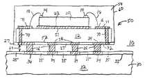
- FIG. 1is a cross-sectional view of an electrical system 10 , including an integrated circuit 50 mounted to a motherboard 30 .
- Integrated circuit 50includes a semiconductor die 20 housed in an integrated circuit package 60 .
- Motherboard 30comprises a standard printed circuit board consisting of a base 32 formed with glass epoxy or other dielectric material. Copper foil is laminated on a surface 33 of motherboard 30 and patterned to provide attachment pads 34 for securing leads 26 of package 60 . Electrical and mechanical attachment of leads 26 is preferably accomplished with a lead-free solder which is reflowed after integrated circuit 50 is positioned on motherboard 30 . Alternatively, a conductive material may be selectively plated on motherboard 30 to attach leads 26 . A standard solder masking material is applied to surface 33 and patterned to form a solder mask 35 between attachment pads 34 to prevent a system malfunction due to solder bridging.
- Package 60comprises an interposer or substrate 12 formed with a dielectric material such as glass epoxy and/or bismaleimide-triazine (BT) resin.
- a copper foil formed to a typical thickness of about twenty-five micrometersis laminated on a first surface 51 of substrate 12 and patterned to form a die attach flag 22 as well as a plurality of bonding pads 16 and circuit interconnect traces 71 .
- Die attach flag 22is used for mounting semiconductor die 20 to substrate 12 with a thermally and/or electrically conductive epoxy or similar material.
- Bonding pads 16are used for coupling electrical signals to die pads 14 of semiconductor die 20 with wire bonds 18 .
- semiconductor die 12may be mounted to substrate 12 in a flip-chip fashion.
- the foil laminated on surface 51is described as comprising copper, but a suitable alternative conductive material may be used when appropriate.
- Package 60includes a plastic molding compound 59 formed as shown to protect semiconductor die 20 from being damaged.
- a copper foil formed to a thickness of about twenty-five micrometersis laminated on a surface 52 of substrate 12 and patterned to form a plurality of interconnect traces 72 and access pads 24 .
- Integrated circuit 50typically has between eighty and three hundred access pads 24 which are arrayed in a grid over surface 52 to minimize the area of package 60 .
- Copperis plated on access pads 24 to project from surface 52 a typical distance of between fifty and one-hundred twenty five micrometers to form leads 26 .
- the foil and leads 26are described as comprising copper, another conductive material may be used in the alternative.
- Openingsare drilled in substrate 12 and copper plated to form vias 70 for coupling electrical signals between surface 51 and surface 52 .
- a standard solder masking materialis applied to surface 52 and patterned to form an insulating solder mask 27 as shown to provide damage protection and to prevent solder bridging when integrated circuit 50 is attached to motherboard 30 .
- leads 26are mounted to motherboard 30 so as to maintain a spacing 29 between surface 33 of motherboard 30 and surface 52 of substrate 12 . Spacing 29 allows leads 26 to flex to absorb differences in the thermal expansion characteristics between motherboard 30 and integrated circuit 50 . Such flexing improves the reliability of integrated circuit 50 by reducing the stress on semiconductor die 20 . Flexing has an additional advantage of reducing shear stress where leads 26 and attachment pads 34 come into contact, thereby avoiding a circuit failure due to a detached lead. Similarly, flexing reduces the shear stress between leads 26 and access pads 24 to further improve reliability. As the length of leads 26 increases, the stress is reduced and reliability improves. Typically, leads 26 project from surface 52 a distance of between fifty and one hundred twenty-five micrometers to ensure that integrated circuit 50 has a low cost while meeting specified reliability levels.
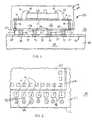
- FIG. 2is a top view of a first portion of integrated circuit 50 , showing surface 51 of substrate 12 and semiconductor die 20 mounted on die attach flag 22 .
- Die pads 14typically are formed around the perimeter of semiconductor die 20 and coupled to bonding pads 16 with wire bonds 18 as shown.
- Substrate 12is drilled to form throughholes or vias 70 whose sidewalls are copper plated to a thickness of about ten micrometers to provide electrical connections between surface 51 and surface 52 of substrate 12 .
- bonding pads 16are formed to have a typical center-to-center spacing of about two hundred micrometers to facilitate wire bonding to die pads 14 , which are formed with a typical center-to-center spacing of about one hundred fifty micrometers.
- the copper foil on surface 51is further patterned to form traces 71 to extend bonding pads 16 to vias 70 .
- FIG. 3is a bottom view of a second portion of integrated circuit 50 , showing features formed on surface 52 in further detail.
- Vias 70are extended through substrate 12 from surface 51 .
- the copper foil laminated on surface 52is patterned to form traces 72 which extend to provide signal paths from vias 70 to access pads 24 as shown.
- Leads 26are formed by plating copper onto access pads 24 as described below.
- FIG. 4is a cross-sectional view of a portion of integrated circuit package 60 after a first processing step of the fabrication of leads 26 .
- Substrate 12 , access pads 24 , traces 72 and solder mask 27are formed as described above.
- a photoresist layer 81is applied to cover surface 52 of substrate 12 and patterned to form openings 82 to expose access pads 24 .
- Photoresist layer 81is formed to a thickness determined by the desired height of leads 26 . In one embodiment, photoresist layer 81 is formed to a thickness of about seventy five micrometers.
- FIG. 5is a cross-sectional view of the portion of integrated circuit package 60 after a second processing step of the fabrication of leads 26 .
- Package 60is placed in a plating apparatus (not shown) to plate copper onto access pads 24 to fill openings 82 with plated copper. Copper is plated outwardly from surface 52 in a direction indicated by arrow 85 .
- the plating steptypically is a timed process whose duration is determined by the thickness of photoresist layer 81 .
- copperis electroplated in openings 82 .
- electroless platingis used to deposit copper in openings 82 .
- a suitable alternate conductive materialmay be plated onto access pads 24 .
- FIG. 6is a cross-sectional view of the portion of integrated circuit package 60 after a third processing step of the fabrication of leads 26 .
- Photoresist layer 81is removed using a standard removal process to leave leads 26 projecting outwardly from surface 52 as shown.
- leads 26 and access pads 24are formed with the same conductive material, i.e., copper, so a secure mechanical interface as well as a low resistance connection between leads 26 and access pads 24 is obtained.
- platingproduces a grain structure in leads 26 which results in a higher flexibility than would result from a more crystalline structure. The higher flexibility effectively provides a greater strain relief when motherboard 30 and package 60 expand at different rates as the temperature varies, which improves reliability.
- platingprovides a high degree of control over the height of leads 26 , which results in a more uniform spacing between motherboard 30 and integrated circuit 50 than is achieved by using solder balls to form package leads. This uniformity improves reliability by ensuring that stress relief is more evenly distributed among leads 26 than is provided using solder ball leads.
- access pads 24are formed with copper foil while leads 26 are formed with plated copper, they have different structural characteristics.
- Plated copperis formed with grains which typically have a columnar structure whose grain boundaries run parallel to the direction of plating.
- solder mask 27is shown as being formed before photoresist layer 81 is deposited and patterned, solder mask 27 may alternatively be formed after leads 26 are plated 35 and photoresist layer 81 is removed. In this embodiment, leads 26 are protected with a screen template to avoid coating and a standard liquid solder masking material is flowed on surface 52 between leads 26 . Such a process has an advantage of avoiding the need to use photoresist process to form solder mask 27 , thereby reducing the manufacturing cost of integrated circuit 50 .
- a substratehas a first surface for mounting a semiconductor die and a second surface defining a first via.
- a leadis formed with a conductive material to project outwardly from the second surface, where the conductive material extends from the lead through the first via for coupling to the semiconductor die.
- the leadsare formed with a plating process to improve their flexibility and better control their height, which results in a high reliability.
- the use of copper leadshas a further advantage of a lower thermal resistance than packages using solder ball leads, which lowers the die temperature to further improve reliability.
- the inventioneliminates the need for lead-based or other types of solder balls to form the leads, thereby reducing the cost of the package and the risk of health or environmental damage.
Landscapes
- Engineering & Computer Science (AREA)
- Microelectronics & Electronic Packaging (AREA)
- Manufacturing & Machinery (AREA)
- Physics & Mathematics (AREA)
- Condensed Matter Physics & Semiconductors (AREA)
- General Physics & Mathematics (AREA)
- Computer Hardware Design (AREA)
- Power Engineering (AREA)
- Structures For Mounting Electric Components On Printed Circuit Boards (AREA)
- Lead Frames For Integrated Circuits (AREA)
Abstract
Description
- The present invention relates in general to semiconductor devices and, more particularly, to integrated circuits that include a grid array package for housing a semiconductor die.[0001]
- Integrated circuits that have high pin or lead counts often are housed in grid array packages to achieve a small size. For example, ball grid array (BGA) packages are used to provide chip scale or nearly chip scale integrated circuits that have between eighty and three hundred leads. A BGA package includes an interposer or substrate whose top surface has a region for mounting a semiconductor die. Wire bonds electrically connect nodes of the semiconductor die to bonding pads formed on the top surface. Throughholes or vias through the substrate are used for connecting the bonding pads to access pads formed on the bottom surface of the substrate. The access pads typically are arranged in a grid to minimize the area occupied by the integrated circuit's leads. A solder mask is patterned with openings over each access pad to accommodate small solder balls which are reflowed to function leads of the BGA package.[0002]
- Current BGA packages suffer from a high cost due to the complex equipment needed to pick up the small solder balls, place them on the access pads and then to reflow the solder without disturbing the solder ball positions. This equipment is expensive and occupies a large area of a manufacturing facility. The cost is further increased because the access pads must be made large enough to ensure that the solder mask openings do not overlap the boundaries of the access pads, thereby reducing the number of routing channels between access pads and increasing the size of the substrate. A further problem is the presence of lead in the solder balls, which is considered to be an environmental and health hazard.[0003]
- Hence, there is a need for an integrated circuit grid array package and method which reduces the size and manufacturing cost of the package as well as the risk of environmental and health damage.[0004]
- FIG. 1 is a cross-sectional view of an electrical system;[0005]
- FIG. 2 is a top view of a first portion of an integrated circuit;[0006]
- FIG. 3 is a bottom view of a second portion of the integrated circuit;[0007]
- FIG. 4 is a cross-sectional view of a portion of an integrated circuit package after a first processing step;[0008]
- FIG. 5 is a cross-sectional view of the portion of the integrated circuit package after a second processing step; and[0009]
- FIG. 6 is a cross-sectional view of the portion of the integrated circuit package after a third processing step.[0010]
- In the figures, elements having the same reference numbers have similar functionality.[0011]
- FIG. 1 is a cross-sectional view of an[0012]
electrical system 10, including an integratedcircuit 50 mounted to amotherboard 30.Integrated circuit 50 includes a semiconductor die20 housed in anintegrated circuit package 60. - Motherboard[0013]30 comprises a standard printed circuit board consisting of a
base 32 formed with glass epoxy or other dielectric material. Copper foil is laminated on asurface 33 ofmotherboard 30 and patterned to provideattachment pads 34 for securingleads 26 ofpackage 60. Electrical and mechanical attachment ofleads 26 is preferably accomplished with a lead-free solder which is reflowed after integratedcircuit 50 is positioned onmotherboard 30. Alternatively, a conductive material may be selectively plated onmotherboard 30 toattach leads 26. A standard solder masking material is applied tosurface 33 and patterned to form asolder mask 35 betweenattachment pads 34 to prevent a system malfunction due to solder bridging. - [0014]
Package 60 comprises an interposer orsubstrate 12 formed with a dielectric material such as glass epoxy and/or bismaleimide-triazine (BT) resin. A copper foil formed to a typical thickness of about twenty-five micrometers is laminated on afirst surface 51 ofsubstrate 12 and patterned to form adie attach flag 22 as well as a plurality ofbonding pads 16 andcircuit interconnect traces 71. Dieattach flag 22 is used for mounting semiconductor die20 tosubstrate 12 with a thermally and/or electrically conductive epoxy or similar material.Bonding pads 16 are used for coupling electrical signals to diepads 14 of semiconductor die20 withwire bonds 18. In an alternate embodiment, semiconductor die12 may be mounted tosubstrate 12 in a flip-chip fashion. The foil laminated onsurface 51 is described as comprising copper, but a suitable alternative conductive material may be used when appropriate.Package 60 includes aplastic molding compound 59 formed as shown to protectsemiconductor die 20 from being damaged. - A copper foil formed to a thickness of about twenty-five micrometers is laminated on a[0015]
surface 52 ofsubstrate 12 and patterned to form a plurality ofinterconnect traces 72 andaccess pads 24.Integrated circuit 50 typically has between eighty and three hundredaccess pads 24 which are arrayed in a grid oversurface 52 to minimize the area ofpackage 60. Copper is plated onaccess pads 24 to project from surface52 a typical distance of between fifty and one-hundred twenty five micrometers toform leads 26. Although the foil andleads 26 are described as comprising copper, another conductive material may be used in the alternative. - Openings are drilled in[0016]
substrate 12 and copper plated to formvias 70 for coupling electrical signals betweensurface 51 andsurface 52. A standard solder masking material is applied tosurface 52 and patterned to form aninsulating solder mask 27 as shown to provide damage protection and to prevent solder bridging when integratedcircuit 50 is attached tomotherboard 30. - Note that[0017]
leads 26 are mounted tomotherboard 30 so as to maintain aspacing 29 betweensurface 33 ofmotherboard 30 andsurface 52 ofsubstrate 12. Spacing29 allows leads26 to flex to absorb differences in the thermal expansion characteristics betweenmotherboard 30 and integratedcircuit 50. Such flexing improves the reliability of integratedcircuit 50 by reducing the stress onsemiconductor die 20. Flexing has an additional advantage of reducing shear stress where leads26 andattachment pads 34 come into contact, thereby avoiding a circuit failure due to a detached lead. Similarly, flexing reduces the shear stress betweenleads 26 andaccess pads 24 to further improve reliability. As the length ofleads 26 increases, the stress is reduced and reliability improves. Typically, leads26 project from surface52 a distance of between fifty and one hundred twenty-five micrometers to ensure that integratedcircuit 50 has a low cost while meeting specified reliability levels. - FIG. 2 is a top view of a first portion of integrated[0018]
circuit 50, showingsurface 51 ofsubstrate 12 and semiconductor die20 mounted on dieattach flag 22. Diepads 14 typically are formed around the perimeter of semiconductor die20 and coupled to bondingpads 16 withwire bonds 18 as shown.Substrate 12 is drilled to form throughholes orvias 70 whose sidewalls are copper plated to a thickness of about ten micrometers to provide electrical connections betweensurface 51 andsurface 52 ofsubstrate 12. Note thatbonding pads 16 are formed to have a typical center-to-center spacing of about two hundred micrometers to facilitate wire bonding todie pads 14, which are formed with a typical center-to-center spacing of about one hundred fifty micrometers. The copper foil onsurface 51 is further patterned to formtraces 71 to extendbonding pads 16 tovias 70. - FIG. 3 is a bottom view of a second portion of integrated[0019]
circuit 50, showing features formed onsurface 52 in further detail.Vias 70 are extended throughsubstrate 12 fromsurface 51. The copper foil laminated onsurface 52 is patterned to formtraces 72 which extend to provide signal paths fromvias 70 to accesspads 24 as shown.Leads 26 are formed by plating copper ontoaccess pads 24 as described below. - FIG. 4 is a cross-sectional view of a portion of[0020]
integrated circuit package 60 after a first processing step of the fabrication ofleads 26.Substrate 12,access pads 24, traces72 andsolder mask 27 are formed as described above. Aphotoresist layer 81 is applied tocover surface 52 ofsubstrate 12 and patterned to form openings82 to exposeaccess pads 24.Photoresist layer 81 is formed to a thickness determined by the desired height ofleads 26. In one embodiment,photoresist layer 81 is formed to a thickness of about seventy five micrometers. - FIG. 5 is a cross-sectional view of the portion of[0021]
integrated circuit package 60 after a second processing step of the fabrication ofleads 26.Package 60 is placed in a plating apparatus (not shown) to plate copper ontoaccess pads 24 to fill openings82 with plated copper. Copper is plated outwardly fromsurface 52 in a direction indicated byarrow 85. The plating step typically is a timed process whose duration is determined by the thickness ofphotoresist layer 81. In one embodiment, copper is electroplated in openings82. In an alternative embodiment, electroless plating is used to deposit copper in openings82. Although described as copper plating, a suitable alternate conductive material may be plated ontoaccess pads 24. - FIG. 6 is a cross-sectional view of the portion of[0022]
integrated circuit package 60 after a third processing step of the fabrication of leads26.Photoresist layer 81 is removed using a standard removal process to leaveleads 26 projecting outwardly fromsurface 52 as shown. In the described embodiment, leads26 andaccess pads 24 are formed with the same conductive material, i.e., copper, so a secure mechanical interface as well as a low resistance connection between leads26 andaccess pads 24 is obtained. In addition, plating produces a grain structure in leads26 which results in a higher flexibility than would result from a more crystalline structure. The higher flexibility effectively provides a greater strain relief whenmotherboard 30 andpackage 60 expand at different rates as the temperature varies, which improves reliability. Moreover, plating provides a high degree of control over the height ofleads 26, which results in a more uniform spacing betweenmotherboard 30 and integratedcircuit 50 than is achieved by using solder balls to form package leads. This uniformity improves reliability by ensuring that stress relief is more evenly distributed amongleads 26 than is provided using solder ball leads. - Although[0023]
access pads 24 are formed with copper foil while leads26 are formed with plated copper, they have different structural characteristics. Plated copper is formed with grains which typically have a columnar structure whose grain boundaries run parallel to the direction of plating. - That is the columnar grains of leads[0024]25 run outwardly from
surface 52 and parallel to the plating direction indicated byarrow 85 of FIG. 5. Such a structure produces a high shear strength in leads26. Moreover, a signal current ISIGNALflowing through one of theleads 26 in the plating direction encounters fewer grain boundaries than a current flowing perpendicular to the plating direction. Therefore, ISIGNALflows through a lower electrical resistance. - Although[0025]
solder mask 27 is shown as being formed beforephotoresist layer 81 is deposited and patterned,solder mask 27 may alternatively be formed afterleads 26 are plated35 andphotoresist layer 81 is removed. In this embodiment, leads26 are protected with a screen template to avoid coating and a standard liquid solder masking material is flowed onsurface 52 between leads26. Such a process has an advantage of avoiding the need to use photoresist process to formsolder mask 27, thereby reducing the manufacturing cost ofintegrated circuit 50. - In summary, the above described integrated circuit, package and method provide a higher reliability and lower cost than is achieved with previous grid array packages and methods. A substrate has a first surface for mounting a semiconductor die and a second surface defining a first via. A lead is formed with a conductive material to project outwardly from the second surface, where the conductive material extends from the lead through the first via for coupling to the semiconductor die. The leads are formed with a plating process to improve their flexibility and better control their height, which results in a high reliability. In addition, the use of copper leads has a further advantage of a lower thermal resistance than packages using solder ball leads, which lowers the die temperature to further improve reliability. Moreover, the invention eliminates the need for lead-based or other types of solder balls to form the leads, thereby reducing the cost of the package and the risk of health or environmental damage.[0026]
Claims (37)
Priority Applications (2)
| Application Number | Priority Date | Filing Date | Title |
|---|---|---|---|
| US09/817,330US6889429B2 (en) | 2001-03-26 | 2001-03-26 | Method of making a lead-free integrated circuit package |
| US11/040,334US7180170B2 (en) | 2001-03-26 | 2005-01-24 | Lead-free integrated circuit package structure |
Applications Claiming Priority (1)
| Application Number | Priority Date | Filing Date | Title |
|---|---|---|---|
| US09/817,330US6889429B2 (en) | 2001-03-26 | 2001-03-26 | Method of making a lead-free integrated circuit package |
Related Child Applications (1)
| Application Number | Title | Priority Date | Filing Date |
|---|---|---|---|
| US11/040,334DivisionUS7180170B2 (en) | 2001-03-26 | 2005-01-24 | Lead-free integrated circuit package structure |
Publications (2)
| Publication Number | Publication Date |
|---|---|
| US20020134582A1true US20020134582A1 (en) | 2002-09-26 |
| US6889429B2 US6889429B2 (en) | 2005-05-10 |
Family
ID=25222837
Family Applications (2)
| Application Number | Title | Priority Date | Filing Date |
|---|---|---|---|
| US09/817,330Expired - LifetimeUS6889429B2 (en) | 2001-03-26 | 2001-03-26 | Method of making a lead-free integrated circuit package |
| US11/040,334Expired - LifetimeUS7180170B2 (en) | 2001-03-26 | 2005-01-24 | Lead-free integrated circuit package structure |
Family Applications After (1)
| Application Number | Title | Priority Date | Filing Date |
|---|---|---|---|
| US11/040,334Expired - LifetimeUS7180170B2 (en) | 2001-03-26 | 2005-01-24 | Lead-free integrated circuit package structure |
Country Status (1)
| Country | Link |
|---|---|
| US (2) | US6889429B2 (en) |
Cited By (12)
| Publication number | Priority date | Publication date | Assignee | Title |
|---|---|---|---|---|
| US6717253B2 (en)* | 2002-01-31 | 2004-04-06 | Advanced Semiconductor Engineering, Inc. | Assembly package with stacked dies and signal transmission plate |
| US20040178492A1 (en)* | 2001-09-28 | 2004-09-16 | Toppan Printing Co., Ltd. | Multi-layer wiring board, IC package, and method of manufacturing multi-layer wiring board |
| US20050067712A1 (en)* | 2003-09-29 | 2005-03-31 | Toshikazu Imaoka | Semiconductor apparatus and method of fabricating the same |
| US20070178750A1 (en)* | 2006-01-27 | 2007-08-02 | Au Optronics Corp. | Flexible printed circuit having inter-lead ribs in a welding area |
| US20080106880A1 (en)* | 2003-04-09 | 2008-05-08 | Dai Nippon Printing Co., Ltd. | Wiring board and method of manufacturing the same |
| US20110157808A1 (en)* | 2009-12-30 | 2011-06-30 | Intel Corporation | Patch on interposer through PGA interconnect structures |
| US20130154119A1 (en)* | 2011-12-15 | 2013-06-20 | Byung Tai Do | Integrated circuit packaging system with terminals and method of manufacture thereof |
| US8623711B2 (en) | 2011-12-15 | 2014-01-07 | Stats Chippac Ltd. | Integrated circuit packaging system with package-on-package and method of manufacture thereof |
| US8629567B2 (en) | 2011-12-15 | 2014-01-14 | Stats Chippac Ltd. | Integrated circuit packaging system with contacts and method of manufacture thereof |
| US20150214171A1 (en)* | 2014-01-24 | 2015-07-30 | Zhuhai Advanced Chip Carriers & Electronic Substrate Solutions Technologies Co., Ltd. | Substrates with Protruding Copper Termination Posts |
| US20170170099A1 (en)* | 2015-12-11 | 2017-06-15 | I-Shou University | Interposer structure and manufacturing method thereof |
| US20180063960A1 (en)* | 2016-08-31 | 2018-03-01 | Fujitsu Limited | Semiconductor device, electronic device, method of manufacturing semiconductor device, and method of manufacturing electronic device |
Families Citing this family (19)
| Publication number | Priority date | Publication date | Assignee | Title |
|---|---|---|---|---|
| US6889429B2 (en)* | 2001-03-26 | 2005-05-10 | Semiconductor Components Industries, L.L.C. | Method of making a lead-free integrated circuit package |
| JP2004311784A (en)* | 2003-04-08 | 2004-11-04 | Fuji Xerox Co Ltd | Photodetector and mounting method thereof |
| US7042098B2 (en)* | 2003-07-07 | 2006-05-09 | Freescale Semiconductor,Inc | Bonding pad for a packaged integrated circuit |
| US7098528B2 (en)* | 2003-12-22 | 2006-08-29 | Lsi Logic Corporation | Embedded redistribution interposer for footprint compatible chip package conversion |
| KR100575086B1 (en)* | 2004-11-11 | 2006-05-03 | 삼성전자주식회사 | Semiconductor package with conductive molding compound and manufacturing method |
| US7508261B2 (en)* | 2005-01-19 | 2009-03-24 | Micro-Mobio, Inc. | Systems of miniaturized compatible radio frequency wireless devices |
| US7332799B2 (en)* | 2005-12-28 | 2008-02-19 | Tessera, Inc. | Packaged chip having features for improved signal transmission on the package |
| TWI339881B (en)* | 2007-02-15 | 2011-04-01 | Via Tech Inc | Chip package |
| JP5207659B2 (en)* | 2007-05-22 | 2013-06-12 | キヤノン株式会社 | Semiconductor device |
| US8786063B2 (en)* | 2009-05-15 | 2014-07-22 | Stats Chippac Ltd. | Integrated circuit packaging system with leads and transposer and method of manufacture thereof |
| KR101758852B1 (en)* | 2009-07-15 | 2017-07-17 | 퀄컴 인코포레이티드 | Semiconductor-on-insulator with backside heat dissipation |
| US9496227B2 (en) | 2009-07-15 | 2016-11-15 | Qualcomm Incorporated | Semiconductor-on-insulator with back side support layer |
| KR101818556B1 (en) | 2009-07-15 | 2018-01-15 | 퀄컴 인코포레이티드 | Semiconductor-on-insulator with back side body connection |
| US9034732B2 (en)* | 2009-07-15 | 2015-05-19 | Silanna Semiconductor U.S.A., Inc. | Semiconductor-on-insulator with back side support layer |
| US8921168B2 (en)* | 2009-07-15 | 2014-12-30 | Silanna Semiconductor U.S.A., Inc. | Thin integrated circuit chip-on-board assembly and method of making |
| US9466719B2 (en) | 2009-07-15 | 2016-10-11 | Qualcomm Incorporated | Semiconductor-on-insulator with back side strain topology |
| US9390974B2 (en) | 2012-12-21 | 2016-07-12 | Qualcomm Incorporated | Back-to-back stacked integrated circuit assembly and method of making |
| US7927919B1 (en)* | 2009-12-03 | 2011-04-19 | Powertech Technology Inc. | Semiconductor packaging method to save interposer |
| US9515181B2 (en) | 2014-08-06 | 2016-12-06 | Qualcomm Incorporated | Semiconductor device with self-aligned back side features |
Citations (3)
| Publication number | Priority date | Publication date | Assignee | Title |
|---|---|---|---|---|
| US5808873A (en)* | 1997-05-30 | 1998-09-15 | Motorola, Inc. | Electronic component assembly having an encapsulation material and method of forming the same |
| US5895229A (en)* | 1997-05-19 | 1999-04-20 | Motorola, Inc. | Microelectronic package including a polymer encapsulated die, and method for forming same |
| US6046499A (en)* | 1996-03-27 | 2000-04-04 | Kabushiki Kaisha Toshiba | Heat transfer configuration for a semiconductor device |
Family Cites Families (27)
| Publication number | Priority date | Publication date | Assignee | Title |
|---|---|---|---|---|
| US6097089A (en)* | 1998-01-28 | 2000-08-01 | Mitsubishi Gas Chemical Company, Inc. | Semiconductor plastic package, metal plate for said package, and method of producing copper-clad board for said package |
| US4821151A (en)* | 1985-12-20 | 1989-04-11 | Olin Corporation | Hermetically sealed package |
| US5098864A (en)* | 1989-11-29 | 1992-03-24 | Olin Corporation | Process for manufacturing a metal pin grid array package |
| US6262477B1 (en)* | 1993-03-19 | 2001-07-17 | Advanced Interconnect Technologies | Ball grid array electronic package |
| US5539153A (en)* | 1994-08-08 | 1996-07-23 | Hewlett-Packard Company | Method of bumping substrates by contained paste deposition |
| KR100239406B1 (en)* | 1996-12-27 | 2000-01-15 | 김영환 | Surface mounted semiconductor package and method of manufacturing the same |
| KR100244965B1 (en)* | 1997-08-12 | 2000-02-15 | 윤종용 | Method for manufacturing printed circuit board(PCB) and ball grid array(BGA) package |
| US6249053B1 (en)* | 1998-02-16 | 2001-06-19 | Sumitomo Metal (Smi) Electronics Devices Inc. | Chip package and method for manufacturing the same |
| US6153518A (en)* | 1998-05-13 | 2000-11-28 | Texas Instruments Incorporated | Method of making chip size package substrate |
| JP2001264667A (en)* | 2000-03-15 | 2001-09-26 | Sony Corp | Optical scanning device |
| US6462421B1 (en)* | 2000-04-10 | 2002-10-08 | Advanced Semicondcutor Engineering, Inc. | Multichip module |
| KR100398716B1 (en)* | 2000-06-12 | 2003-09-19 | 가부시키가이샤 히타치세이사쿠쇼 | Semiconductor module and circuit substrate |
| JP2002043352A (en)* | 2000-07-27 | 2002-02-08 | Nec Corp | Semiconductor element, manufacturing method therefor and semiconductor device |
| US6433425B1 (en)* | 2000-09-12 | 2002-08-13 | International Business Machines Corporation | Electronic package interconnect structure comprising lead-free solders |
| TW462121B (en)* | 2000-09-19 | 2001-11-01 | Siliconware Precision Industries Co Ltd | Heat sink type ball grid array package |
| TW490820B (en)* | 2000-10-04 | 2002-06-11 | Advanced Semiconductor Eng | Heat dissipation enhanced ball grid array package |
| US6734540B2 (en)* | 2000-10-11 | 2004-05-11 | Altera Corporation | Semiconductor package with stress inhibiting intermediate mounting substrate |
| US6486415B2 (en)* | 2001-01-16 | 2002-11-26 | International Business Machines Corporation | Compliant layer for encapsulated columns |
| US20020163818A1 (en)* | 2001-03-05 | 2002-11-07 | Green Mark D. | Magnetic device and method of manufacture therefor |
| US6889429B2 (en)* | 2001-03-26 | 2005-05-10 | Semiconductor Components Industries, L.L.C. | Method of making a lead-free integrated circuit package |
| JP4923336B2 (en)* | 2001-04-10 | 2012-04-25 | 日本電気株式会社 | Circuit board and electronic device using the circuit board |
| US6617680B2 (en)* | 2001-08-22 | 2003-09-09 | Siliconware Precision Industries Co., Ltd. | Chip carrier, semiconductor package and fabricating method thereof |
| JP3891838B2 (en)* | 2001-12-26 | 2007-03-14 | 株式会社ルネサステクノロジ | Semiconductor device and manufacturing method thereof |
| US6854636B2 (en)* | 2002-12-06 | 2005-02-15 | International Business Machines Corporation | Structure and method for lead free solder electronic package interconnections |
| TWI251313B (en)* | 2003-09-26 | 2006-03-11 | Seiko Epson Corp | Intermediate chip module, semiconductor device, circuit board, and electronic device |
| TWI245389B (en)* | 2003-10-02 | 2005-12-11 | Siliconware Precision Industries Co Ltd | Conductive trace structure and semiconductor package having the conductive trace structure |
| JP4601365B2 (en)* | 2004-09-21 | 2010-12-22 | ルネサスエレクトロニクス株式会社 | Semiconductor device |
- 2001
- 2001-03-26USUS09/817,330patent/US6889429B2/ennot_activeExpired - Lifetime
- 2005
- 2005-01-24USUS11/040,334patent/US7180170B2/ennot_activeExpired - Lifetime
Patent Citations (3)
| Publication number | Priority date | Publication date | Assignee | Title |
|---|---|---|---|---|
| US6046499A (en)* | 1996-03-27 | 2000-04-04 | Kabushiki Kaisha Toshiba | Heat transfer configuration for a semiconductor device |
| US5895229A (en)* | 1997-05-19 | 1999-04-20 | Motorola, Inc. | Microelectronic package including a polymer encapsulated die, and method for forming same |
| US5808873A (en)* | 1997-05-30 | 1998-09-15 | Motorola, Inc. | Electronic component assembly having an encapsulation material and method of forming the same |
Cited By (19)
| Publication number | Priority date | Publication date | Assignee | Title |
|---|---|---|---|---|
| US20040178492A1 (en)* | 2001-09-28 | 2004-09-16 | Toppan Printing Co., Ltd. | Multi-layer wiring board, IC package, and method of manufacturing multi-layer wiring board |
| US20070175025A1 (en)* | 2001-09-28 | 2007-08-02 | Toppan Printing Co., Ltd. | Method of manufacturing multi-layer wiring board |
| US7584535B2 (en) | 2001-09-28 | 2009-09-08 | Toppan Printing Co., Ltd. | Method of manufacturing multi-layer wiring board |
| US6717253B2 (en)* | 2002-01-31 | 2004-04-06 | Advanced Semiconductor Engineering, Inc. | Assembly package with stacked dies and signal transmission plate |
| US20080106880A1 (en)* | 2003-04-09 | 2008-05-08 | Dai Nippon Printing Co., Ltd. | Wiring board and method of manufacturing the same |
| US7480151B2 (en)* | 2003-04-09 | 2009-01-20 | Dai Nippon Printing Co., Ltd. | Wiring board and method of manufacturing the same |
| US20050067712A1 (en)* | 2003-09-29 | 2005-03-31 | Toshikazu Imaoka | Semiconductor apparatus and method of fabricating the same |
| US20070178750A1 (en)* | 2006-01-27 | 2007-08-02 | Au Optronics Corp. | Flexible printed circuit having inter-lead ribs in a welding area |
| US20110157808A1 (en)* | 2009-12-30 | 2011-06-30 | Intel Corporation | Patch on interposer through PGA interconnect structures |
| US8381393B2 (en)* | 2009-12-30 | 2013-02-26 | Intel Corporation | Patch on interposer through PGA interconnect structures |
| US20130154119A1 (en)* | 2011-12-15 | 2013-06-20 | Byung Tai Do | Integrated circuit packaging system with terminals and method of manufacture thereof |
| US8623711B2 (en) | 2011-12-15 | 2014-01-07 | Stats Chippac Ltd. | Integrated circuit packaging system with package-on-package and method of manufacture thereof |
| US8629567B2 (en) | 2011-12-15 | 2014-01-14 | Stats Chippac Ltd. | Integrated circuit packaging system with contacts and method of manufacture thereof |
| US9219029B2 (en)* | 2011-12-15 | 2015-12-22 | Stats Chippac Ltd. | Integrated circuit packaging system with terminals and method of manufacture thereof |
| US20150214171A1 (en)* | 2014-01-24 | 2015-07-30 | Zhuhai Advanced Chip Carriers & Electronic Substrate Solutions Technologies Co., Ltd. | Substrates with Protruding Copper Termination Posts |
| US9642261B2 (en)* | 2014-01-24 | 2017-05-02 | Zhuhai Advanced Chip Carriers & Electronic Substrate Solutions Technologies Co. Ltd. | Composite electronic structure with partially exposed and protruding copper termination posts |
| US20170170099A1 (en)* | 2015-12-11 | 2017-06-15 | I-Shou University | Interposer structure and manufacturing method thereof |
| US20180063960A1 (en)* | 2016-08-31 | 2018-03-01 | Fujitsu Limited | Semiconductor device, electronic device, method of manufacturing semiconductor device, and method of manufacturing electronic device |
| US10595412B2 (en)* | 2016-08-31 | 2020-03-17 | Fujitsu Limited | Semiconductor device, electronic device, method of manufacturing semiconductor device, and method of manufacturing electronic device |
Also Published As
| Publication number | Publication date |
|---|---|
| US6889429B2 (en) | 2005-05-10 |
| US20050121767A1 (en) | 2005-06-09 |
| US7180170B2 (en) | 2007-02-20 |
Similar Documents
| Publication | Publication Date | Title |
|---|---|---|
| US6889429B2 (en) | Method of making a lead-free integrated circuit package | |
| US5796589A (en) | Ball grid array integrated circuit package that has vias located within the solder pads of a package | |
| US7183658B2 (en) | Low cost microelectronic circuit package | |
| US5972734A (en) | Interposer for ball grid array (BGA) package | |
| KR100692441B1 (en) | Semiconductor device and manufacturing method of semiconductor device | |
| US6297141B1 (en) | Mounting assembly of integrated circuit device and method for production thereof | |
| US6738263B2 (en) | Stackable ball grid array package | |
| JP3898891B2 (en) | Via plug adapter | |
| US6084295A (en) | Semiconductor device and circuit board used therein | |
| EP2798675B1 (en) | Method for a substrate core layer | |
| US7795710B2 (en) | Lead frame routed chip pads for semiconductor packages | |
| US20070137029A1 (en) | Method for fabricating semiconductor component with adjustment circuit for adjusting physical or electrical characteristics of substrate conductors | |
| US6717264B2 (en) | High density integrated circuit package | |
| KR20010099684A (en) | Tape ball grid array with interconnected ground plane | |
| US6441486B1 (en) | BGA substrate via structure | |
| US5951804A (en) | Method for simultaneously manufacturing chip-scale package using lead frame strip with a plurality of lead frames | |
| EP1171915B1 (en) | Electrical conductor system of a semiconductor device and manufacturing method thereof | |
| EP1487017A2 (en) | Thermally Enhanced Substrate for a BGA | |
| US6543676B2 (en) | Pin attachment by a surface mounting method for fabricating organic pin grid array packages | |
| US6400575B1 (en) | Integrated circuits packaging system and method | |
| US6207354B1 (en) | Method of making an organic chip carrier package | |
| KR100339491B1 (en) | Manufacturing method of chip size package | |
| JPH06318666A (en) | Ceramic package | |
| KR19980034131A (en) | How to Form Flip Chip Structure |
Legal Events
| Date | Code | Title | Description |
|---|---|---|---|
| AS | Assignment | Owner name:SEMICONDUCTOR COMPONENTS INDUSTRIES, LLC, ARIZONA Free format text:ASSIGNMENT OF ASSIGNORS INTEREST;ASSIGNORS:CELAYA, PHILLIP C.;DONLEY, JAMES S.;ST. GERMAIN, STEPHEN C.;REEL/FRAME:011703/0355 Effective date:20010322 | |
| AS | Assignment | Owner name:JPMORGAN CHASE BANK, AS COLLATERAL AGENT, NEW YORK Free format text:SUPPLEMENT TO SECURITY AGREEMENT;ASSIGNORS:SEMICONDUCTOR COMPONENTS INDUSTRIES, LLC;SEMICONDUCTOR COMPONENTS OF RHODE ISLAND, INC.;REEL/FRAME:012991/0180 Effective date:20020505 | |
| AS | Assignment | Owner name:WELLS FARGO BANK MINNESOTA, NATIONAL ASSOCIATION, Free format text:SECURITY AGREEMENT;ASSIGNORS:SEMICONDUCTOR COMPONENTS INDUSTRIES, LLC;SEMICONDUCTOR COMPONENTS INDUSTRIES OF RHODE ISLAND, INC.;REEL/FRAME:012958/0638 Effective date:20020506 | |
| AS | Assignment | Owner name:JPMORGAN CHASE BANK, NEW YORK Free format text:SECURITY INTEREST;ASSIGNOR:SEMICONDUCTOR COMPONENTS INDUSTRIES, LLC;REEL/FRAME:014007/0239 Effective date:20030303 | |
| STCF | Information on status: patent grant | Free format text:PATENTED CASE | |
| CC | Certificate of correction | ||
| FPAY | Fee payment | Year of fee payment:4 | |
| FPAY | Fee payment | Year of fee payment:8 | |
| AS | Assignment | Owner name:DEUTSCHE BANK AG NEW YORK BRANCH, NEW YORK Free format text:SECURITY INTEREST;ASSIGNOR:SEMICONDUCTOR COMPONENTS INDUSTRIES, LLC;REEL/FRAME:038620/0087 Effective date:20160415 | |
| AS | Assignment | Owner name:SEMICONDUCTOR COMPONENTS INDUSTRIES, LLC, ARIZONA Free format text:RELEASE BY SECURED PARTY;ASSIGNOR:WELLS FARGO BANK MINNESOTA, NATIONAL ASSOCIATION, AS COLLATERAL AGENT;REEL/FRAME:038543/0039 Effective date:20050217 | |
| AS | Assignment | Owner name:SEMICONDUCTOR COMPONENTS INDUSTRIES, LLC, ARIZONA Free format text:RELEASE BY SECURED PARTY;ASSIGNOR:JPMORGAN CHASE BANK, N.A., AS ADMINISTRATIVE AGENT AND COLLATERAL AGENT;REEL/FRAME:038631/0345 Effective date:20100511 Owner name:SEMICONDUCTOR COMPONENTS INDUSTRIES, LLC, ARIZONA Free format text:RELEASE BY SECURED PARTY;ASSIGNOR:JPMORGAN CHASE BANK, N.A. (ON ITS BEHALF AND ON BEHALF OF ITS PREDECESSOR IN INTEREST, CHASE MANHATTAN BANK);REEL/FRAME:038632/0074 Effective date:20160415 | |
| AS | Assignment | Owner name:DEUTSCHE BANK AG NEW YORK BRANCH, AS COLLATERAL AG Free format text:CORRECTIVE ASSIGNMENT TO CORRECT THE INCORRECT PATENT NUMBER 5859768 AND TO RECITE COLLATERAL AGENT ROLE OF RECEIVING PARTY IN THE SECURITY INTEREST PREVIOUSLY RECORDED ON REEL 038620 FRAME 0087. ASSIGNOR(S) HEREBY CONFIRMS THE SECURITY INTEREST;ASSIGNOR:SEMICONDUCTOR COMPONENTS INDUSTRIES, LLC;REEL/FRAME:039853/0001 Effective date:20160415 Owner name:DEUTSCHE BANK AG NEW YORK BRANCH, AS COLLATERAL AGENT, NEW YORK Free format text:CORRECTIVE ASSIGNMENT TO CORRECT THE INCORRECT PATENT NUMBER 5859768 AND TO RECITE COLLATERAL AGENT ROLE OF RECEIVING PARTY IN THE SECURITY INTEREST PREVIOUSLY RECORDED ON REEL 038620 FRAME 0087. ASSIGNOR(S) HEREBY CONFIRMS THE SECURITY INTEREST;ASSIGNOR:SEMICONDUCTOR COMPONENTS INDUSTRIES, LLC;REEL/FRAME:039853/0001 Effective date:20160415 | |
| FPAY | Fee payment | Year of fee payment:12 | |
| AS | Assignment | Owner name:FAIRCHILD SEMICONDUCTOR CORPORATION, ARIZONA Free format text:RELEASE OF SECURITY INTEREST IN PATENTS RECORDED AT REEL 038620, FRAME 0087;ASSIGNOR:DEUTSCHE BANK AG NEW YORK BRANCH, AS COLLATERAL AGENT;REEL/FRAME:064070/0001 Effective date:20230622 Owner name:SEMICONDUCTOR COMPONENTS INDUSTRIES, LLC, ARIZONA Free format text:RELEASE OF SECURITY INTEREST IN PATENTS RECORDED AT REEL 038620, FRAME 0087;ASSIGNOR:DEUTSCHE BANK AG NEW YORK BRANCH, AS COLLATERAL AGENT;REEL/FRAME:064070/0001 Effective date:20230622 |