US20020130395A1 - Integrated circuit contact - Google Patents
Integrated circuit contactDownload PDFInfo
- Publication number
- US20020130395A1 US20020130395A1US10/136,544US13654402AUS2002130395A1US 20020130395 A1US20020130395 A1US 20020130395A1US 13654402 AUS13654402 AUS 13654402AUS 2002130395 A1US2002130395 A1US 2002130395A1
- Authority
- US
- United States
- Prior art keywords
- etch
- mask
- providing
- etching
- layer
- Prior art date
- Legal status (The legal status is an assumption and is not a legal conclusion. Google has not performed a legal analysis and makes no representation as to the accuracy of the status listed.)
- Granted
Links
Images

Classifications
- H—ELECTRICITY
- H01—ELECTRIC ELEMENTS
- H01L—SEMICONDUCTOR DEVICES NOT COVERED BY CLASS H10
- H01L21/00—Processes or apparatus adapted for the manufacture or treatment of semiconductor or solid state devices or of parts thereof
- H01L21/02—Manufacture or treatment of semiconductor devices or of parts thereof
- H01L21/04—Manufacture or treatment of semiconductor devices or of parts thereof the devices having potential barriers, e.g. a PN junction, depletion layer or carrier concentration layer
- H01L21/18—Manufacture or treatment of semiconductor devices or of parts thereof the devices having potential barriers, e.g. a PN junction, depletion layer or carrier concentration layer the devices having semiconductor bodies comprising elements of Group IV of the Periodic Table or AIIIBV compounds with or without impurities, e.g. doping materials
- H01L21/30—Treatment of semiconductor bodies using processes or apparatus not provided for in groups H01L21/20 - H01L21/26
- H01L21/31—Treatment of semiconductor bodies using processes or apparatus not provided for in groups H01L21/20 - H01L21/26 to form insulating layers thereon, e.g. for masking or by using photolithographic techniques; After treatment of these layers; Selection of materials for these layers
- H01L21/3105—After-treatment
- H01L21/311—Etching the insulating layers by chemical or physical means
- H01L21/31144—Etching the insulating layers by chemical or physical means using masks
- H—ELECTRICITY
- H01—ELECTRIC ELEMENTS
- H01L—SEMICONDUCTOR DEVICES NOT COVERED BY CLASS H10
- H01L21/00—Processes or apparatus adapted for the manufacture or treatment of semiconductor or solid state devices or of parts thereof
- H01L21/70—Manufacture or treatment of devices consisting of a plurality of solid state components formed in or on a common substrate or of parts thereof; Manufacture of integrated circuit devices or of parts thereof
- H01L21/71—Manufacture of specific parts of devices defined in group H01L21/70
- H01L21/768—Applying interconnections to be used for carrying current between separate components within a device comprising conductors and dielectrics
- H01L21/76801—Applying interconnections to be used for carrying current between separate components within a device comprising conductors and dielectrics characterised by the formation and the after-treatment of the dielectrics, e.g. smoothing
- H01L21/76802—Applying interconnections to be used for carrying current between separate components within a device comprising conductors and dielectrics characterised by the formation and the after-treatment of the dielectrics, e.g. smoothing by forming openings in dielectrics
- H01L21/76807—Applying interconnections to be used for carrying current between separate components within a device comprising conductors and dielectrics characterised by the formation and the after-treatment of the dielectrics, e.g. smoothing by forming openings in dielectrics for dual damascene structures
- H01L21/76808—Applying interconnections to be used for carrying current between separate components within a device comprising conductors and dielectrics characterised by the formation and the after-treatment of the dielectrics, e.g. smoothing by forming openings in dielectrics for dual damascene structures involving intermediate temporary filling with material
- H—ELECTRICITY
- H01—ELECTRIC ELEMENTS
- H01L—SEMICONDUCTOR DEVICES NOT COVERED BY CLASS H10
- H01L21/00—Processes or apparatus adapted for the manufacture or treatment of semiconductor or solid state devices or of parts thereof
- H01L21/70—Manufacture or treatment of devices consisting of a plurality of solid state components formed in or on a common substrate or of parts thereof; Manufacture of integrated circuit devices or of parts thereof
- H01L21/71—Manufacture of specific parts of devices defined in group H01L21/70
- H01L21/768—Applying interconnections to be used for carrying current between separate components within a device comprising conductors and dielectrics
- H01L21/76801—Applying interconnections to be used for carrying current between separate components within a device comprising conductors and dielectrics characterised by the formation and the after-treatment of the dielectrics, e.g. smoothing
- H01L21/76829—Applying interconnections to be used for carrying current between separate components within a device comprising conductors and dielectrics characterised by the formation and the after-treatment of the dielectrics, e.g. smoothing characterised by the formation of thin functional dielectric layers, e.g. dielectric etch-stop, barrier, capping or liner layers
- Y—GENERAL TAGGING OF NEW TECHNOLOGICAL DEVELOPMENTS; GENERAL TAGGING OF CROSS-SECTIONAL TECHNOLOGIES SPANNING OVER SEVERAL SECTIONS OF THE IPC; TECHNICAL SUBJECTS COVERED BY FORMER USPC CROSS-REFERENCE ART COLLECTIONS [XRACs] AND DIGESTS
- Y10—TECHNICAL SUBJECTS COVERED BY FORMER USPC
- Y10S—TECHNICAL SUBJECTS COVERED BY FORMER USPC CROSS-REFERENCE ART COLLECTIONS [XRACs] AND DIGESTS
- Y10S438/00—Semiconductor device manufacturing: process
- Y10S438/942—Masking
- Y10S438/948—Radiation resist
- Y10S438/95—Multilayer mask including nonradiation sensitive layer
- Y—GENERAL TAGGING OF NEW TECHNOLOGICAL DEVELOPMENTS; GENERAL TAGGING OF CROSS-SECTIONAL TECHNOLOGIES SPANNING OVER SEVERAL SECTIONS OF THE IPC; TECHNICAL SUBJECTS COVERED BY FORMER USPC CROSS-REFERENCE ART COLLECTIONS [XRACs] AND DIGESTS
- Y10—TECHNICAL SUBJECTS COVERED BY FORMER USPC
- Y10S—TECHNICAL SUBJECTS COVERED BY FORMER USPC CROSS-REFERENCE ART COLLECTIONS [XRACs] AND DIGESTS
- Y10S438/00—Semiconductor device manufacturing: process
- Y10S438/97—Specified etch stop material
Definitions
- This inventionrelates generally to processes for manufacturing ultra large scale integrated circuits (ULSICs) and more particularly to a self-aligned process for simultaneously enhancing the achievable device packing density, device reliability and yields during such manufacture.
- ULSICsultra large scale integrated circuits
- This Dual Damascene processing for etching troughs through insulating layers formed on silicon substratesutilizes, among other things, first and second successive etching steps in order to arrive at an ultimate trough and contact hole geometry within surrounding insulating layers formed on the surface of a silicon wafer.
- the first etch stepforms the trough down to a controlled depth within the surface insulating layers.
- the second etch stepextends the depth of the trough down to the active devices within the silicon substrate to form the contact hole.
- One disadvantage of using the above described Dual Damascene approachis that the photoresist etch mask required for the second etch step must be precisely aligned with respect to the trough opening formed by the first etch step.
- etch stop layeron the surface of the insulating layer.
- the width dimension of an opening in the etch stop layeris made coextensive with the width dimension of the desired trough opening to be formed within the insulating layer.
- the etch stop layeris used in combination with an etchant to define the trough opening within the insulating layer.
- a photoresist etch maskis formed on the surface of the etch stop layer and has an opening therein defined by predetermined width and length dimensions dependent upon the desired trough geometry.
- the photoresist maskis formed above the etch stop layer, the alignment of its width dimension is not now critical inasmuch as the etching action for increasing the depth of a portion of the trough to complete formation of the stud or contact hole is confined, or self-aligned, by the opening in the etch stop layer.
- this second etching step of the insulating layercontinues on to the silicon substrate surface, its width dimension remains constant.
- the interconnect troughis completely formed in the first etch, the trough can be and is masked during the second etch that forms the stud or contact hole. The etch that forms the contact hole can, therefore, be controlled independent of the etch that forms the trough.
- the photoresist maskis removed and the completed trough and contact hole is filled with a selected metal such as tungsten.
- the etch stop layercan be either retained in place or removed and the tungsten layer is chemically and mechanically polished using known CMP processes back to a depth substantially coplanar with the surface of the etch stop layer when the etch stop layer is retained in place.
- surface contact padsmay be formed on top of the completed metal pattern.
- the etch stop layer removal stepcan be carried out prior to the tungsten deposition step, and blanket etching of metal can be used instead of CMP processes.
- Another object of this inventionis to provide a new and improved process of the type described which represents a novel alternative with respect to the above described Dual Damascene process.
- Another object of this inventionis to provide a new and improved process of the type described which operates to increase maximum achievable device packing density in the manufacture of integrated circuits.
- Another object of this inventionis to provide a new and improved electrical contract forming process of the type described which enhances device reliability and device yields.
- Another object of this inventionis to provide a new and improved process of the type described which may be repeated through a plurality of stacked dielectric layers such as SiO 2 to thereby form a multi-level metal integrated circuit.
- the present process of forming electrical contacts in the manufacture of integrated circuitsincludes the steps of: forming an insulating layer on the surface of a silicon substrate; forming an etch stop layer on the surface of the insulating layer; forming an opening in the etch stop layer; etching through the opening to a first trough depth into the insulating layer exposed by the opening in the etch stop layer; forming a photoresist etch mask on the surface of the etch stop layer and in a portion of the trough; continuing to etch the exposed portion of the insulating layer until reaching the surface of the silicon substrate to thereby form the contact or stud hole; removing the photoresist mask; and filling the trough and hole thus formed with a selected metal such as tungsten.
- chemical-mechanical polishing processesare used to remove a portion of the selected metal back to a depth coplanar with the surface of the etch stop
- FIGS. 1 through 10are a series of schematic cross section diagrams illustrating the sequence of process steps used in a preferred process embodiment of the invention.
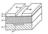
- a silicon substrate 10in which one or more active device regions 12 have been formed using conventional diffusion or ion implantation doping techniques together with conventional photolithographic masking and etching procedures.
- a relatively insulating layer 14preferably made of silicon dioxide, will be formed on the surface of the silicon substrate 10 using low temperature chemical vapor deposition processes and preferably a known tetraethylorthosilicate (TEOS) process.
- TEOStetraethylorthosilicate
- a thin etch stop layer 16is formed to a thickness of about 500-1000 angstroms on the surface of the insulating layer 14 .
- Etch stop layer 16may be made of any suitable material such as silicon nitride, Si 3 N 4 , or titanium oxide, TiO, or aluminum oxide, Al 2 O 3 .
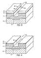
- An openingis then formed in etch stop layer 16 to expose portions of insulating layer 14 at locations of desired trough patterns.
- a first photoresist mask 18is formed on the surface of the etch stop layer 16 , and an opening 20 is formed in the photoresist mask 18 using conventional photolithographic masking and etching procedures in order to expose a given area 22 of the etch stop layer 16 .
- an openingis first etched as indicated at 24 in the etch stop layer 16 using an etchant such as CHF 3 and CF 4 , and the first photoresist mask 18 in FIG.
- etch stop layer 16of either silicon nitride, titanium oxide, aluminum oxide or other equivalent dense inorganic insulating material will be quite suitable to serve as an etch mask during the etching of the insulating layer 14 in the geometry shown in FIGS. 3 and 4.
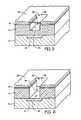
- a second photoresist mask 28 having an opening 30 thereinis formed on the surface of the etch stop layer 16 .
- This second photoresist mask 28will serve to mask against etching carried out using state of the art reactive ion etching (RIE) techniques.
- Opening 30 in second photoresist mask 28has a width dimension, W, and need not be precisely aligned with the corresponding width dimension of the trough 26 opening because, during this etching process, etch stop layer 16 will serve to mask against the vertical ion bombardment except in the region of the trough 26 .
- Such ion bombardment and etchingwill continue etching through the SiO 2 insulating layer 14 until reaching the active device region 12 to thereby produce the contact hole 33 indicated in FIG. 6.
- the length dimension of the contact hole 33extends to a back wall 34 of the insulating layer 14 , and this back wall 34 is aligned with the back wall 36 of the second photoresist mask 28 .
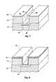
- the second photoresist mask 28 in FIG. 6has been removed to show the completed trough and hole geometry consisting of a first depth at the top wall 38 which extends into the device structure of FIG. 7 along the length of the top wall 38 and the second greater depth at exposed surface 32 .
- the alignment of the contact hole 33 length dimension as defined by the back wall 36 of the photoresist mask 28 in FIG. 6still remains critical to defining the precisely desired device geometries for the integrated circuits being manufactured.
- adhesion layer 40the exposed surface 32 and top wall 38 in FIG. 7 and the top surfaces of the etch stop layer 16 are covered with adhesion layer 40 , and then as shown in FIG. 9, a metal layer 42 is deposited on the outer surface of the adhesion layer 40 .
- This metal layer 42will preferably be either tungsten, copper or silver which is laid down using conventional metal deposition processes.
- Adhesion layer 40preferably made of titanium nitride, is sputter deposited on insulating layer 14 and etch stop layer 16 to improve bonding with metal layer 42 . Frequently, it will be desired to then polish or etch back metal layer 42 so that the ultimate top surface of the selected metal layer 42 is coplanar with the top surface of the etch stop layer 16 as shown in FIG. 10.
- the etch stop layer 16can be used as a mask during etching of the metal layer 42 so that the metal layer 42 can be etched through opening 24 in etch stop layer 16 down to and coplanar with the top surface of insulating layer 14 . Etch stop layer 16 would then be removed. The etch stop layer 16 may also be removed prior to forming the adhesion and metal layers 40 and 42 , respectively. Also optionally, surface contact pads or interconnects (not shown) may be made on top of or leading into the planarized metallization-filled troughs described above.
- the present inventionis in no way limited by the particular materials or layer thicknesses described above which are only exemplary of certain typical materials and layer thicknesses used in existing ULSIC semiconductor fabrication processes.
- the etch stop layermay be either removed or retained in place after the vertical trough forming process has been completed.
- the present inventionis not limited to the electrical interconnection through a single layer of dielectric material, e.g. SiO 2 , as shown in FIG. 10 and may instead be used in various types of multi-level metallization processes such as those shown, for example, in co-pending application Ser. No. 07/775,744, U.S. Pat. No.
Landscapes
- Engineering & Computer Science (AREA)
- Physics & Mathematics (AREA)
- Condensed Matter Physics & Semiconductors (AREA)
- General Physics & Mathematics (AREA)
- Manufacturing & Machinery (AREA)
- Computer Hardware Design (AREA)
- Microelectronics & Electronic Packaging (AREA)
- Power Engineering (AREA)
- Internal Circuitry In Semiconductor Integrated Circuit Devices (AREA)
Abstract
Description
- This application is a continuation of application Ser. No. 09/569,578, filed May 10, 2000, pending, which is a divisional of application Ser. No. 09/099,047, filed Jun. 17, 1998, now U.S. Pat. No. 6,221,779, which is a continuation of application Ser. No. 08/786,482, filed Jan. 21, 1997, now U.S. Pat. No. 5,858,877, which is a continuation of application Ser. No. 08/626,651, filed Apr. 1, 1996, now U.S. Pat. No. 5,651,855, which is a continuation of application Ser. No. 08/259,187, filed Jun. 13, 1994, abandoned, which is a continuation-in-part of application Ser. No. 07/921,320 filed Jul. 28, 1992, abandoned.[0001]
- Field of the Invention: This invention, relates generally to processes for manufacturing ultra large scale integrated circuits (ULSICs) and more particularly to a self-aligned process for simultaneously enhancing the achievable device packing density, device reliability and yields during such manufacture.[0002]
- In the manufacture of ultra large scale integrated circuits, such as 4 megabit and up dynamic random access memories (DRAMs), it has been one prior art approach to use an inlaid, fully integrated wiring technology which is known in the integrated circuit manufacturing arts as “Dual Damascene” technology. This approach to ULSIC electrical contact development is described in some detail in Cronin, et al., U.S. Pat. Ser. No. 5,126,006 and in an article by Carter W. Kaanta, et al. entitled “Dual Damascene: A ULSIC Wiring Technology,” IBM General Technology Division, Essex Junction, Vt., VMIC Conference, Jun. 11-12, 1991, at pp. 144-152.[0003]
- This Dual Damascene processing for etching troughs through insulating layers formed on silicon substrates utilizes, among other things, first and second successive etching steps in order to arrive at an ultimate trough and contact hole geometry within surrounding insulating layers formed on the surface of a silicon wafer. The first etch step forms the trough down to a controlled depth within the surface insulating layers. The second etch step extends the depth of the trough down to the active devices within the silicon substrate to form the contact hole. One disadvantage of using the above described Dual Damascene approach is that the photoresist etch mask required for the second etch step must be precisely aligned with respect to the trough opening formed by the first etch step. The requirement for precise alignment of the second etch mask imposes an upper threshold on the maximum achievable packing density, reliability and yields that can be reached using the above Dual Damascene process. In addition, present techniques do not allow the etch of the interconnect trough to be controlled independent of the etch of the stud or contact hole.[0004]
- It is the solution to these problems to which the present invention is directed.[0005]
- In accordance with the present invention, it has been discovered that the above problem of precise second etch mask alignment with respect to the first formed trough opening can be significantly reduced by the employment of an etch stop layer on the surface of the insulating layer. The width dimension of an opening in the etch stop layer is made coextensive with the width dimension of the desired trough opening to be formed within the insulating layer. Then, the etch stop layer is used in combination with an etchant to define the trough opening within the insulating layer. Next, a photoresist etch mask is formed on the surface of the etch stop layer and has an opening therein defined by predetermined width and length dimensions dependent upon the desired trough geometry. However, since the photoresist mask is formed above the etch stop layer, the alignment of its width dimension is not now critical inasmuch as the etching action for increasing the depth of a portion of the trough to complete formation of the stud or contact hole is confined, or self-aligned, by the opening in the etch stop layer. Thus, as this second etching step of the insulating layer continues on to the silicon substrate surface, its width dimension remains constant. Also, because the interconnect trough is completely formed in the first etch, the trough can be and is masked during the second etch that forms the stud or contact hole. The etch that forms the contact hole can, therefore, be controlled independent of the etch that forms the trough.[0006]
- Next, the photoresist mask is removed and the completed trough and contact hole is filled with a selected metal such as tungsten. Finally, and optionally, the etch stop layer can be either retained in place or removed and the tungsten layer is chemically and mechanically polished using known CMP processes back to a depth substantially coplanar with the surface of the etch stop layer when the etch stop layer is retained in place. Optionally, surface contact pads may be formed on top of the completed metal pattern. Also optionally, the etch stop layer removal step can be carried out prior to the tungsten deposition step, and blanket etching of metal can be used instead of CMP processes.[0007]
- Accordingly, it is an object of the present invention to provide a new and improved self-aligning process for making electrical contacts in the manufacture of high density integrated circuits.[0008]
- Another object of this invention is to provide a new and improved process of the type described which represents a novel alternative with respect to the above described Dual Damascene process.[0009]
- Another object of this invention is to provide a new and improved process of the type described which operates to increase maximum achievable device packing density in the manufacture of integrated circuits.[0010]
- Another object of this invention is to provide a new and improved electrical contract forming process of the type described which enhances device reliability and device yields.[0011]
- Another object of this invention is to provide a new and improved process of the type described which may be repeated through a plurality of stacked dielectric layers such as SiO[0012]2to thereby form a multi-level metal integrated circuit.
- Briefly summarized, and commensurate in scope with the broad claims filed herein, the present process of forming electrical contacts in the manufacture of integrated circuits includes the steps of: forming an insulating layer on the surface of a silicon substrate; forming an etch stop layer on the surface of the insulating layer; forming an opening in the etch stop layer; etching through the opening to a first trough depth into the insulating layer exposed by the opening in the etch stop layer; forming a photoresist etch mask on the surface of the etch stop layer and in a portion of the trough; continuing to etch the exposed portion of the insulating layer until reaching the surface of the silicon substrate to thereby form the contact or stud hole; removing the photoresist mask; and filling the trough and hole thus formed with a selected metal such as tungsten. In a preferred embodiment of the invention, chemical-mechanical polishing processes are used to remove a portion of the selected metal back to a depth coplanar with the surface of the etch stop layer or surface of the insulating layer.[0013]
- The above brief summary of the invention, together with its attendant objects, advantages and novel features will become better understood with reference to the following description of the accompanying drawings.[0014]
- FIGS. 1 through 10 are a series of schematic cross section diagrams illustrating the sequence of process steps used in a preferred process embodiment of the invention.[0015]
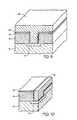
- Referring now to FIG. 1, there is shown a[0016]
silicon substrate 10 in which one or moreactive device regions 12 have been formed using conventional diffusion or ion implantation doping techniques together with conventional photolithographic masking and etching procedures. Typically, a relativelyinsulating layer 14, preferably made of silicon dioxide, will be formed on the surface of thesilicon substrate 10 using low temperature chemical vapor deposition processes and preferably a known tetraethylorthosilicate (TEOS) process. Next, a thinetch stop layer 16 is formed to a thickness of about 500-1000 angstroms on the surface of the insulatinglayer 14.Etch stop layer 16 may be made of any suitable material such as silicon nitride, Si3N4, or titanium oxide, TiO, or aluminum oxide, Al2O3. - An opening is then formed in[0017]
etch stop layer 16 to expose portions ofinsulating layer 14 at locations of desired trough patterns. In the preferred embodiment, and referring now to FIG. 2, a firstphotoresist mask 18 is formed on the surface of theetch stop layer 16, and anopening 20 is formed in thephotoresist mask 18 using conventional photolithographic masking and etching procedures in order to expose a givenarea 22 of theetch stop layer 16. Then, as shown in FIG. 3, an opening is first etched as indicated at24 in theetch stop layer 16 using an etchant such as CHF3and CF4, and thefirst photoresist mask 18 in FIG. 3 may be left in place during etching down to a first desired depth to formtrough 26 within theinsulating layer 14. Once thetrough 26 depth has been reached, then thefirst photoresist mask 18 in FIG. 3 is removed as shown in FIG. 4. Theetch stop layer 16 of either silicon nitride, titanium oxide, aluminum oxide or other equivalent dense inorganic insulating material will be quite suitable to serve as an etch mask during the etching of theinsulating layer 14 in the geometry shown in FIGS. 3 and 4. - Referring now to FIG. 5, a[0018]
second photoresist mask 28 having anopening 30 therein is formed on the surface of theetch stop layer 16. This secondphotoresist mask 28 will serve to mask against etching carried out using state of the art reactive ion etching (RIE) techniques. Opening30 in secondphotoresist mask 28 has a width dimension, W, and need not be precisely aligned with the corresponding width dimension of thetrough 26 opening because, during this etching process,etch stop layer 16 will serve to mask against the vertical ion bombardment except in the region of thetrough 26. Such ion bombardment and etching will continue etching through the SiO2insulating layer14 until reaching theactive device region 12 to thereby produce thecontact hole 33 indicated in FIG. 6. As seen in FIG. 6, the length dimension of thecontact hole 33 extends to aback wall 34 of theinsulating layer 14, and thisback wall 34 is aligned with theback wall 36 of the secondphotoresist mask 28. - Referring now to FIG. 7, the second[0019]
photoresist mask 28 in FIG. 6 has been removed to show the completed trough and hole geometry consisting of a first depth at thetop wall 38 which extends into the device structure of FIG. 7 along the length of thetop wall 38 and the second greater depth at exposed surface32. There is no criticality of mask alignment of the width dimension W of thephotoresist mask 28 with the width dimension of the vertical trough being etched. However, the alignment of thecontact hole 33 length dimension as defined by theback wall 36 of thephotoresist mask 28 in FIG. 6 still remains critical to defining the precisely desired device geometries for the integrated circuits being manufactured. - Referring now to FIG. 8, the exposed surface[0020]32 and
top wall 38 in FIG. 7 and the top surfaces of theetch stop layer 16 are covered withadhesion layer 40, and then as shown in FIG. 9, ametal layer 42 is deposited on the outer surface of theadhesion layer 40. Thismetal layer 42 will preferably be either tungsten, copper or silver which is laid down using conventional metal deposition processes.Adhesion layer 40, preferably made of titanium nitride, is sputter deposited on insulatinglayer 14 andetch stop layer 16 to improve bonding withmetal layer 42. Frequently, it will be desired to then polish or etch backmetal layer 42 so that the ultimate top surface of the selectedmetal layer 42 is coplanar with the top surface of theetch stop layer 16 as shown in FIG. 10. - Optionally, the[0021]
etch stop layer 16 can be used as a mask during etching of themetal layer 42 so that themetal layer 42 can be etched throughopening 24 inetch stop layer 16 down to and coplanar with the top surface of insulatinglayer 14.Etch stop layer 16 would then be removed. Theetch stop layer 16 may also be removed prior to forming the adhesion andmetal layers - Various modifications may be made in and to the above described embodiment without departing from the spirit and scope of this invention. For example, the present invention is in no way limited by the particular materials or layer thicknesses described above which are only exemplary of certain typical materials and layer thicknesses used in existing ULSIC semiconductor fabrication processes. In addition, the etch stop layer may be either removed or retained in place after the vertical trough forming process has been completed. Furthermore, the present invention is not limited to the electrical interconnection through a single layer of dielectric material, e.g. SiO[0022]2, as shown in FIG. 10 and may instead be used in various types of multi-level metallization processes such as those shown, for example, in co-pending application Ser. No. 07/775,744, U.S. Pat. No. 5,204,286 of Trung T. Doan entitled “Method of Making Self-Aligned Contacts and Vertical Interconnects to Integrated Circuits and Devices Made Thereby,” filed Oct. 15, 1991, assigned to the present assignee and incorporated herein by reference. Accordingly, these and other process and device modifications are clearly within the scope of the following appended claims.
Claims (26)
1. A processing method for a support material for a semiconductor device, comprising:
providing a plurality of serially deposited etch masks made of a plurality of etch mask materials; and
etching an opening into said support material for a semiconductor device, wherein said etching is determined by said plurality of etch masks.
2. The method inclaim 1 , wherein said providing a plurality of serially deposited etch masks comprises:
providing a first etch mask made of a first etch mask material over said support material; and
providing a second etch mask made of a second etch mask material over said first etch mask and over said support material.
3. The method inclaim 2 , wherein said providing a second etch mask comprises providing a second etch mask made of resist; and wherein said providing a first etch mask comprises providing a first etch mask made of a non-resist material.
4. The method inclaim 3 , wherein said providing a first etch mask comprises providing a first etch mask made from a selection consisting of silicon nitride, titanium oxide and aluminum oxide.
5. The method inclaim 3 , wherein said etching an opening into said support material comprises etching a second opening into said support material; and wherein said method further comprises:
providing a temporary mask;
etching a first opening using said temporary mask; and
removing said temporary mask before said etching a second opening.
6. The method inclaim 5 , wherein said providing a temporary mask occurs after said step of providing a first etch mask; and wherein said removing said temporary mask occurs before said step of providing a second etch mask.
7. A shaping method for an oxide layer in an electronic circuit comprising:
etching said oxide layer through openings in a first plurality of etch guide layers over said oxide layer; and
etching said oxide layer through openings in a second plurality of etch guide layers over said oxide layer.
8. The method inclaim 7 , further comprising providing a common etch guide layer for said first plurality of etch guide layers and said second plurality of etch guide layers.
9. A control method for an etching process, comprising:
using a first resist mask to pattern an etch stop during said etching process;
using said first resist mask to pattern an insulation layer during said etching process; and
using said etch stop and a second resist mask to further pattern said insulation layer during said etching process.
10. The method inclaim 9 , wherein:
said using a first resist mask to pattern an etch stop comprises using a first resist mask during a first etch step;
said using said first resist mask to pattern an insulation layer comprises using said first resist mask during a second etch step; and
said using said etch stop and a second resist mask comprises using said etch stop and a second resist mask during a third etch step.
11. The method inclaim 10 , wherein said using said etch stop and a second resist mask during a third etch step comprises using said etch stop and a second resist mask during a reactive ion etch.
12. A method of forming an opening in a layer of a semiconductor device in a process, comprising:
providing a first set of etching parameters with a first resist mask over said layer of said semiconductor device;
etching said layer according to said first set of etching parameters;
removing said first resist mask;
providing a second set of etching parameters with a second resist mask, wherein said providing a second set of etching parameters occurs after said removing said first resist mask; and
etching said layer according to said first and second sets of etching parameters.
13. The method inclaim 12 , further comprising retaining said first set of etching parameters after said removing said first resist mask.
14. The method inclaim 13 , wherein said retaining said first set of etching parameters comprises:
providing an etch stop material between said first resist mask and said layer;
etching said etch stop according to said first set of etching parameters; and
retaining said etch stop during said step of etching said layer according to said first and second sets of etching parameters.
15. A processing method for a semiconductor circuit portion including an insulator, comprising:
providing an etch stop as part of said semiconductor circuit portion, said etch stop overlying said insulator;
patterning said etch stop using a first resist mask;
patterning said insulator using said first resist mask; and
patterning said insulator with said etch stop and a second resist mask.
16. The method inclaim 15 , wherein said providing an etch stop as part of said semiconductor circuit portion comprises providing an etch stop as a permanent part of said semiconductor circuit portion.
17. A construction method for a portion of a circuit device, comprising:
providing a layer as part of said circuit device;
forming a trough in said layer using an etch controlled by a first photoresist mask; and
forming a contact hole under said trough using an etch controlled by a second photoresist mask and an etch stop.
18. The method inclaim 17 , wherein said forming a contact hole comprises forming a contact hole under said trough without directly using said first photoresist mask.
19. The method inclaim 17 , further comprising a defining a trough-shaped opening in said etch stop using an etch controlled by said first photoresist mask.
20. The method inclaim 19 , wherein said forming a contact hole comprises forming a contact hole in said layer.
21. A fabrication method for a semiconductor circuit, comprising:
using at least one patterned mask to form a trough within an oxide during an etch;
using at least two differently patterned masks to form a stud hole under said trough during an etch; and
retaining at least one of said at least two differently patterned masks in a completed version of said semiconductor circuit.
22. A method for forming a portion of a circuit device, comprising:
providing a layer as part of said circuit device;
forming a trough in said layer using an etch controlled by a first photoresist mask; and
forming a contact hole under said trough using an etch controlled by a second photoresist mask and an etch stop.
23. The method inclaim 22 , wherein said forming a contact hole comprises forming a contact hole under said trough without directly using said first photoresist mask.
24. The method inclaim 22 , further comprising a defining a trough-shaped opening in said etch stop using an etch controlled by said first photoresist mask.
25. The method inclaim 24 , wherein said forming a contact hole comprises forming a contact hole in said layer.
26. A fabrication method for at least a portion of a semiconductor circuit, comprising: using at least one patterned mask to form a trough within an oxide during an etch; using at least two differently patterned masks to form a stud hole under said trough during an etch; and retaining at least one of said at least two differently patterned masks in a completed version of said semiconductor circuit.
Priority Applications (6)
| Application Number | Priority Date | Filing Date | Title |
|---|---|---|---|
| US10/136,544US7282440B2 (en) | 1992-07-28 | 2002-05-01 | Integrated circuit contact |
| US10/923,587US7569485B2 (en) | 1992-07-28 | 2004-08-19 | Method for an integrated circuit contact |
| US10/923,060US7282447B2 (en) | 1992-07-28 | 2004-08-19 | Method for an integrated circuit contact |
| US10/923,242US7276448B2 (en) | 1992-07-28 | 2004-08-19 | Method for an integrated circuit contact |
| US11/841,906US7871934B2 (en) | 1992-07-28 | 2007-08-20 | Method for an integrated circuit contact |
| US12/565,280US8097514B2 (en) | 1992-07-28 | 2009-09-23 | Method for an integrated circuit contact |
Applications Claiming Priority (7)
| Application Number | Priority Date | Filing Date | Title |
|---|---|---|---|
| US92132092A | 1992-07-28 | 1992-07-28 | |
| US25918794A | 1994-06-13 | 1994-06-13 | |
| US08/626,651US5651855A (en) | 1992-07-28 | 1996-04-01 | Method of making self aligned contacts to silicon substrates during the manufacture of integrated circuits |
| US08/786,482US5858877A (en) | 1992-07-28 | 1997-01-21 | Self-aligned process for making contacts to silicon substrates during the manufacture of integrated circuits therein |
| US09/099,047US6221779B1 (en) | 1992-07-28 | 1998-06-17 | Self-aligned process for making contacts to silicon substrates during the manufacture of integrated circuits therein |
| US09/569,578US6414392B1 (en) | 1992-07-28 | 2000-05-10 | Integrated circuit contact |
| US10/136,544US7282440B2 (en) | 1992-07-28 | 2002-05-01 | Integrated circuit contact |
Related Parent Applications (1)
| Application Number | Title | Priority Date | Filing Date |
|---|---|---|---|
| US09/569,578ContinuationUS6414392B1 (en) | 1992-07-28 | 2000-05-10 | Integrated circuit contact |
Related Child Applications (3)
| Application Number | Title | Priority Date | Filing Date |
|---|---|---|---|
| US10/923,242DivisionUS7276448B2 (en) | 1992-07-28 | 2004-08-19 | Method for an integrated circuit contact |
| US10/923,060DivisionUS7282447B2 (en) | 1992-07-28 | 2004-08-19 | Method for an integrated circuit contact |
| US10/923,587DivisionUS7569485B2 (en) | 1992-07-28 | 2004-08-19 | Method for an integrated circuit contact |
Publications (2)
| Publication Number | Publication Date |
|---|---|
| US20020130395A1true US20020130395A1 (en) | 2002-09-19 |
| US7282440B2 US7282440B2 (en) | 2007-10-16 |
Family
ID=26947142
Family Applications (12)
| Application Number | Title | Priority Date | Filing Date |
|---|---|---|---|
| US08/626,651Expired - LifetimeUS5651855A (en) | 1992-07-28 | 1996-04-01 | Method of making self aligned contacts to silicon substrates during the manufacture of integrated circuits |
| US08/786,482Expired - LifetimeUS5858877A (en) | 1992-07-28 | 1997-01-21 | Self-aligned process for making contacts to silicon substrates during the manufacture of integrated circuits therein |
| US09/099,047Expired - LifetimeUS6221779B1 (en) | 1992-07-28 | 1998-06-17 | Self-aligned process for making contacts to silicon substrates during the manufacture of integrated circuits therein |
| US09/569,578Expired - LifetimeUS6414392B1 (en) | 1992-07-28 | 2000-05-10 | Integrated circuit contact |
| US10/136,544Expired - Fee RelatedUS7282440B2 (en) | 1992-07-28 | 2002-05-01 | Integrated circuit contact |
| US10/136,126Expired - Fee RelatedUS6573601B2 (en) | 1992-07-28 | 2002-05-01 | Integrated circuit contact |
| US10/443,471Expired - Fee RelatedUS7315082B2 (en) | 1992-07-28 | 2003-05-22 | Semiconductor device having integrated circuit contact |
| US10/923,587Expired - Fee RelatedUS7569485B2 (en) | 1992-07-28 | 2004-08-19 | Method for an integrated circuit contact |
| US10/923,060Expired - Fee RelatedUS7282447B2 (en) | 1992-07-28 | 2004-08-19 | Method for an integrated circuit contact |
| US10/923,242Expired - Fee RelatedUS7276448B2 (en) | 1992-07-28 | 2004-08-19 | Method for an integrated circuit contact |
| US11/841,906Expired - Fee RelatedUS7871934B2 (en) | 1992-07-28 | 2007-08-20 | Method for an integrated circuit contact |
| US12/565,280Expired - Fee RelatedUS8097514B2 (en) | 1992-07-28 | 2009-09-23 | Method for an integrated circuit contact |
Family Applications Before (4)
| Application Number | Title | Priority Date | Filing Date |
|---|---|---|---|
| US08/626,651Expired - LifetimeUS5651855A (en) | 1992-07-28 | 1996-04-01 | Method of making self aligned contacts to silicon substrates during the manufacture of integrated circuits |
| US08/786,482Expired - LifetimeUS5858877A (en) | 1992-07-28 | 1997-01-21 | Self-aligned process for making contacts to silicon substrates during the manufacture of integrated circuits therein |
| US09/099,047Expired - LifetimeUS6221779B1 (en) | 1992-07-28 | 1998-06-17 | Self-aligned process for making contacts to silicon substrates during the manufacture of integrated circuits therein |
| US09/569,578Expired - LifetimeUS6414392B1 (en) | 1992-07-28 | 2000-05-10 | Integrated circuit contact |
Family Applications After (7)
| Application Number | Title | Priority Date | Filing Date |
|---|---|---|---|
| US10/136,126Expired - Fee RelatedUS6573601B2 (en) | 1992-07-28 | 2002-05-01 | Integrated circuit contact |
| US10/443,471Expired - Fee RelatedUS7315082B2 (en) | 1992-07-28 | 2003-05-22 | Semiconductor device having integrated circuit contact |
| US10/923,587Expired - Fee RelatedUS7569485B2 (en) | 1992-07-28 | 2004-08-19 | Method for an integrated circuit contact |
| US10/923,060Expired - Fee RelatedUS7282447B2 (en) | 1992-07-28 | 2004-08-19 | Method for an integrated circuit contact |
| US10/923,242Expired - Fee RelatedUS7276448B2 (en) | 1992-07-28 | 2004-08-19 | Method for an integrated circuit contact |
| US11/841,906Expired - Fee RelatedUS7871934B2 (en) | 1992-07-28 | 2007-08-20 | Method for an integrated circuit contact |
| US12/565,280Expired - Fee RelatedUS8097514B2 (en) | 1992-07-28 | 2009-09-23 | Method for an integrated circuit contact |
Country Status (1)
| Country | Link |
|---|---|
| US (12) | US5651855A (en) |
Families Citing this family (74)
| Publication number | Priority date | Publication date | Assignee | Title |
|---|---|---|---|---|
| US5651855A (en)* | 1992-07-28 | 1997-07-29 | Micron Technology, Inc. | Method of making self aligned contacts to silicon substrates during the manufacture of integrated circuits |
| US5662770A (en) | 1993-04-16 | 1997-09-02 | Micron Technology, Inc. | Method and apparatus for improving etch uniformity in remote source plasma reactors with powered wafer chucks |
| JPH09306988A (en)* | 1996-03-13 | 1997-11-28 | Sony Corp | Method of forming multilayer wiring |
| US5840624A (en)* | 1996-03-15 | 1998-11-24 | Taiwan Semiconductor Manufacturing Company, Ltd | Reduction of via over etching for borderless contacts |
| US6429120B1 (en)* | 2000-01-18 | 2002-08-06 | Micron Technology, Inc. | Methods and apparatus for making integrated-circuit wiring from copper, silver, gold, and other metals |
| US6309971B1 (en) | 1996-08-01 | 2001-10-30 | Cypress Semiconductor Corporation | Hot metallization process |
| US5922622A (en)* | 1996-09-03 | 1999-07-13 | Vanguard International Semiconductor Corporation | Pattern formation of silicon nitride |
| US5847462A (en)* | 1996-11-14 | 1998-12-08 | Advanced Micro Devices, Inc. | Integrated circuit having conductors of enhanced cross-sectional area with etch stop barrier layer |
| KR100219508B1 (en)* | 1996-12-30 | 1999-09-01 | 윤종용 | Forming method for matal wiring layer of semiconductor device |
| US6051497A (en)* | 1997-06-30 | 2000-04-18 | Siemens Aktiengesellschaft | Formation of sub-groundrule features |
| US6294455B1 (en) | 1997-08-20 | 2001-09-25 | Micron Technology, Inc. | Conductive lines, coaxial lines, integrated circuitry, and methods of forming conductive lines, coaxial lines, and integrated circuitry |
| US6080655A (en) | 1997-08-21 | 2000-06-27 | Micron Technology, Inc. | Method for fabricating conductive components in microelectronic devices and substrate structures thereof |
| US6143616A (en) | 1997-08-22 | 2000-11-07 | Micron Technology, Inc. | Methods of forming coaxial integrated circuitry interconnect lines |
| US6187677B1 (en) | 1997-08-22 | 2001-02-13 | Micron Technology, Inc. | Integrated circuitry and methods of forming integrated circuitry |
| US6054768A (en)* | 1997-10-02 | 2000-04-25 | Micron Technology, Inc. | Metal fill by treatment of mobility layers |
| US6198168B1 (en)* | 1998-01-20 | 2001-03-06 | Micron Technologies, Inc. | Integrated circuits using high aspect ratio vias through a semiconductor wafer and method for forming same |
| US6090636A (en)* | 1998-02-26 | 2000-07-18 | Micron Technology, Inc. | Integrated circuits using optical waveguide interconnects formed through a semiconductor wafer and methods for forming same |
| US6150188A (en) | 1998-02-26 | 2000-11-21 | Micron Technology Inc. | Integrated circuits using optical fiber interconnects formed through a semiconductor wafer and methods for forming same |
| US6846739B1 (en)* | 1998-02-27 | 2005-01-25 | Micron Technology, Inc. | MOCVD process using ozone as a reactant to deposit a metal oxide barrier layer |
| US6197696B1 (en)* | 1998-03-26 | 2001-03-06 | Matsushita Electric Industrial Co., Ltd. | Method for forming interconnection structure |
| US6221711B1 (en) | 1998-05-11 | 2001-04-24 | Micron Technology, Inc. | Methods of electrically contacting to conductive plugs, methods of forming contact openings, and methods of forming dynamic random access memory circuitry |
| US6248636B1 (en)* | 1998-05-28 | 2001-06-19 | Samsung Electronics Co., Ltd. | Method for forming contact holes of semiconductor memory device |
| US6165863A (en)* | 1998-06-22 | 2000-12-26 | Micron Technology, Inc. | Aluminum-filled self-aligned trench for stacked capacitor structure and methods |
| US6127263A (en)* | 1998-07-10 | 2000-10-03 | Applied Materials, Inc. | Misalignment tolerant techniques for dual damascene fabrication |
| TW430946B (en)* | 1998-07-22 | 2001-04-21 | United Microelectronics Corp | Dual damascene process |
| US6391771B1 (en) | 1998-07-23 | 2002-05-21 | Applied Materials, Inc. | Integrated circuit interconnect lines having sidewall layers |
| TW437040B (en) | 1998-08-12 | 2001-05-28 | Applied Materials Inc | Interconnect line formed by dual damascene using dielectric layers having dissimilar etching characteristics |
| US5985753A (en)* | 1998-08-19 | 1999-11-16 | Advanced Micro Devices, Inc. | Method to manufacture dual damascene using a phantom implant mask |
| US6204166B1 (en) | 1998-08-21 | 2001-03-20 | Micron Technology, Inc. | Method for forming dual damascene structures |
| US6326300B1 (en) | 1998-09-21 | 2001-12-04 | Taiwan Semiconductor Manufacturing Company | Dual damascene patterned conductor layer formation method |
| US6225207B1 (en)* | 1998-10-01 | 2001-05-01 | Applied Materials, Inc. | Techniques for triple and quadruple damascene fabrication |
| US6180516B1 (en)* | 1998-11-05 | 2001-01-30 | United Microelectronics Corp, | Method of fabricating a dual damascene structure |
| US6303272B1 (en)* | 1998-11-13 | 2001-10-16 | International Business Machines Corporation | Process for self-alignment of sub-critical contacts to wiring |
| US6287961B1 (en) | 1999-01-04 | 2001-09-11 | Taiwan Semiconductor Manufacturing Company | Dual damascene patterned conductor layer formation method without etch stop layer |
| US6010962A (en)* | 1999-02-12 | 2000-01-04 | Taiwan Semiconductor Manufacturing Company | Copper chemical-mechanical-polishing (CMP) dishing |
| US6223432B1 (en) | 1999-03-17 | 2001-05-01 | Micron Technology, Inc. | Method of forming dual conductive plugs |
| US6509259B1 (en)* | 1999-06-09 | 2003-01-21 | Alliedsignal Inc. | Process of using siloxane dielectric films in the integration of organic dielectric films in electronic devices |
| KR100578222B1 (en)* | 1999-06-28 | 2006-05-12 | 주식회사 하이닉스반도체 | Improved Dual Machine Process in Semiconductor Devices |
| US6410453B1 (en) | 1999-09-02 | 2002-06-25 | Micron Technology, Inc. | Method of processing a substrate |
| US6329281B1 (en)* | 1999-12-03 | 2001-12-11 | Agere Systems Guardian Corp. | Methods for fabricating a multilevel interconnection for an integrated circuit device utilizing a selective overlayer |
| US7211512B1 (en)* | 2000-01-18 | 2007-05-01 | Micron Technology, Inc. | Selective electroless-plated copper metallization |
| US6376370B1 (en) | 2000-01-18 | 2002-04-23 | Micron Technology, Inc. | Process for providing seed layers for using aluminum, copper, gold and silver metallurgy process for providing seed layers for using aluminum, copper, gold and silver metallurgy |
| US7262130B1 (en)* | 2000-01-18 | 2007-08-28 | Micron Technology, Inc. | Methods for making integrated-circuit wiring from copper, silver, gold, and other metals |
| US6420262B1 (en)* | 2000-01-18 | 2002-07-16 | Micron Technology, Inc. | Structures and methods to enhance copper metallization |
| US6476775B1 (en)* | 2000-03-13 | 2002-11-05 | Rcd Technology Corporation | Method for forming radio frequency antenna |
| US6423629B1 (en)* | 2000-05-31 | 2002-07-23 | Kie Y. Ahn | Multilevel copper interconnects with low-k dielectrics and air gaps |
| US6674167B1 (en)* | 2000-05-31 | 2004-01-06 | Micron Technology, Inc. | Multilevel copper interconnect with double passivation |
| US6461963B1 (en) | 2000-08-30 | 2002-10-08 | Micron Technology, Inc. | Utilization of disappearing silicon hard mask for fabrication of semiconductor structures |
| US6803314B2 (en)* | 2001-04-30 | 2004-10-12 | Chartered Semiconductor Manufacturing Ltd. | Double-layered low dielectric constant dielectric dual damascene method |
| US20030008243A1 (en)* | 2001-07-09 | 2003-01-09 | Micron Technology, Inc. | Copper electroless deposition technology for ULSI metalization |
| JP2003109943A (en)* | 2001-09-28 | 2003-04-11 | Mitsubishi Electric Corp | Pattern formation method |
| US7294567B2 (en)* | 2002-03-11 | 2007-11-13 | Micron Technology, Inc. | Semiconductor contact device and method |
| US7297122B2 (en)* | 2002-04-19 | 2007-11-20 | Pelikan Technologies, Inc. | Method and apparatus for penetrating tissue |
| US6838372B2 (en) | 2002-09-25 | 2005-01-04 | Cookson Electronics, Inc. | Via interconnect forming process and electronic component product thereof |
| US7074717B2 (en)* | 2003-03-04 | 2006-07-11 | Micron Technology, Inc. | Damascene processes for forming conductive structures |
| US20050023631A1 (en)* | 2003-07-31 | 2005-02-03 | Varghese Ronnie P. | Controlled dry etch of a film |
| US7220665B2 (en) | 2003-08-05 | 2007-05-22 | Micron Technology, Inc. | H2 plasma treatment |
| EP1682444A2 (en)* | 2003-10-31 | 2006-07-26 | Koninklijke Philips Electronics N.V. | A method of manufacturing an electronic device and electronic device |
| US20050196632A1 (en)* | 2003-12-18 | 2005-09-08 | Afg Industries, Inc. | Protective layer for optical coatings with enhanced corrosion and scratch resistance |
| TWI255502B (en)* | 2005-01-19 | 2006-05-21 | Promos Technologies Inc | Method for preparing structure with high aspect ratio |
| US7833893B2 (en)* | 2007-07-10 | 2010-11-16 | International Business Machines Corporation | Method for forming conductive structures |
| DE202009019091U1 (en) | 2009-12-21 | 2016-05-23 | Agilent Technologies, Inc. - A Delaware Corporation - | Fitting element with front insert |
| KR20120025315A (en)* | 2010-09-07 | 2012-03-15 | 삼성전자주식회사 | Semiconductor deivces and methods of fabricating the same |
| FR2977885A1 (en) | 2011-07-12 | 2013-01-18 | Commissariat Energie Atomique | METHOD FOR PRODUCING A DIRECT-REPORT BURNED ELECTRODE STRUCTURE AND STRUCTURE THUS OBTAINED |
| WO2013101028A1 (en)* | 2011-12-29 | 2013-07-04 | Intel Corporation | Avd hardmask for damascene patterning |
| US9123690B1 (en) | 2012-10-18 | 2015-09-01 | University Of South Florida | Systems and methods for forming contact definitions |
| CN103839874B (en)* | 2012-11-21 | 2016-04-20 | 中芯国际集成电路制造(上海)有限公司 | Metal interconnect structure and preparation method thereof |
| US9059095B2 (en) | 2013-04-22 | 2015-06-16 | International Business Machines Corporation | Self-aligned borderless contacts using a photo-patternable dielectric material as a replacement contact |
| CN105575766B (en)* | 2014-10-17 | 2018-04-13 | 中芯国际集成电路制造(上海)有限公司 | A kind of semiconductor devices and its manufacture method, electronic device |
| US9666546B1 (en) | 2016-04-28 | 2017-05-30 | Infineon Technologies Ag | Multi-layer metal pads |
| JP6942701B2 (en) | 2016-06-06 | 2021-09-29 | 浜松ホトニクス株式会社 | Light modulator, light observation device and light irradiation device |
| CN109313363B (en)* | 2016-06-06 | 2021-12-28 | 浜松光子学株式会社 | Reflection type spatial light modulator, optical observation device, and light irradiation device |
| WO2017213101A1 (en) | 2016-06-06 | 2017-12-14 | 浜松ホトニクス株式会社 | Optical element and optical device |
| US12080643B2 (en)* | 2019-09-26 | 2024-09-03 | Intel Corporation | Integrated circuit structures having differentiated interconnect lines in a same dielectric layer |
Citations (60)
| Publication number | Priority date | Publication date | Assignee | Title |
|---|---|---|---|---|
| US3653898A (en)* | 1969-12-16 | 1972-04-04 | Texas Instruments Inc | Formation of small dimensioned apertures |
| US3660735A (en)* | 1969-09-10 | 1972-05-02 | Sprague Electric Co | Complementary metal insulator silicon transistor pairs |
| US3728167A (en)* | 1970-11-16 | 1973-04-17 | Gte Sylvania Inc | Masking method of making semiconductor device |
| US3904454A (en)* | 1973-12-26 | 1975-09-09 | Ibm | Method for fabricating minute openings in insulating layers during the formation of integrated circuits |
| US3961414A (en)* | 1972-06-09 | 1976-06-08 | International Business Machines Corporation | Semiconductor structure having metallization inlaid in insulating layers and method for making same |
| US3964414A (en)* | 1974-06-11 | 1976-06-22 | Kaiser Aluminum & Chemical Corporation | Easy open end method and apparatus |
| US4030967A (en)* | 1976-08-16 | 1977-06-21 | Northern Telecom Limited | Gaseous plasma etching of aluminum and aluminum oxide |
| US4135954A (en)* | 1977-07-12 | 1979-01-23 | International Business Machines Corporation | Method for fabricating self-aligned semiconductor devices utilizing selectively etchable masking layers |
| US4243435A (en)* | 1979-06-22 | 1981-01-06 | International Business Machines Corporation | Bipolar transistor fabrication process with an ion implanted emitter |
| US4377438A (en)* | 1980-09-22 | 1983-03-22 | Tokyo Shibaura Denki Kabushiki Kaisha | Method for producing semiconductor device |
| US4671849A (en)* | 1985-05-06 | 1987-06-09 | International Business Machines Corporation | Method for control of etch profile |
| US4696097A (en)* | 1985-10-08 | 1987-09-29 | Motorola, Inc. | Poly-sidewall contact semiconductor device method |
| US4832789A (en)* | 1988-04-08 | 1989-05-23 | American Telephone And Telegrph Company, At&T Bell Laboratories | Semiconductor devices having multi-level metal interconnects |
| US4837176A (en)* | 1987-01-30 | 1989-06-06 | Motorola Inc. | Integrated circuit structures having polycrystalline electrode contacts and process |
| US4883767A (en)* | 1986-12-05 | 1989-11-28 | General Electric Company | Method of fabricating self aligned semiconductor devices |
| US4962058A (en)* | 1989-04-14 | 1990-10-09 | International Business Machines Corporation | Process for fabricating multi-level integrated circuit wiring structure from a single metal deposit |
| US4997789A (en)* | 1988-10-31 | 1991-03-05 | Texas Instruments Incorporated | Aluminum contact etch mask and etchstop for tungsten etchback |
| US5055426A (en)* | 1990-09-10 | 1991-10-08 | Micron Technology, Inc. | Method for forming a multilevel interconnect structure on a semiconductor wafer |
| US5055423A (en)* | 1987-12-28 | 1991-10-08 | Texas Instruments Incorporated | Planarized selective tungsten metallization system |
| US5091339A (en)* | 1990-07-23 | 1992-02-25 | Microelectronics And Computer Technology Corporation | Trenching techniques for forming vias and channels in multilayer electrical interconnects |
| US5093279A (en)* | 1991-02-01 | 1992-03-03 | International Business Machines Corporation | Laser ablation damascene process |
| US5106780A (en)* | 1988-08-05 | 1992-04-21 | Kabushiki Kaisha Toshiba | Semiconductor device and method of manufacturing the same |
| US5126006A (en)* | 1990-10-30 | 1992-06-30 | International Business Machines Corp. | Plural level chip masking |
| US5136124A (en)* | 1988-12-14 | 1992-08-04 | International Business Machines Corporation | Method of forming conductors within an insulating substrate |
| US5169802A (en)* | 1991-06-17 | 1992-12-08 | Hewlett-Packard Company | Internal bridging contact |
| US5173442A (en)* | 1990-07-23 | 1992-12-22 | Microelectronics And Computer Technology Corporation | Methods of forming channels and vias in insulating layers |
| US5189506A (en)* | 1990-06-29 | 1993-02-23 | International Business Machines Corporation | Triple self-aligned metallurgy for semiconductor devices |
| US5204286A (en)* | 1991-10-15 | 1993-04-20 | Micron Technology, Inc. | Method of making self-aligned contacts and vertical interconnects to integrated circuits |
| US5206187A (en)* | 1991-08-30 | 1993-04-27 | Micron Technology, Inc. | Method of processing semiconductor wafers using a contact etch stop |
| US5219787A (en)* | 1990-07-23 | 1993-06-15 | Microelectronics And Computer Technology Corporation | Trenching techniques for forming channels, vias and components in substrates |
| US5258328A (en)* | 1992-03-16 | 1993-11-02 | Kabushiki Kaisha Toshiba | Method of forming multilayered wiring structure of semiconductor device |
| US5294561A (en)* | 1992-08-25 | 1994-03-15 | Nec Corporation | Method for manufacturing highly-integrated stacked capacitor |
| US5312777A (en)* | 1992-09-25 | 1994-05-17 | International Business Machines Corporation | Fabrication methods for bidirectional field emission devices and storage structures |
| US5312518A (en)* | 1991-05-31 | 1994-05-17 | Sony Corporation | Dry etching method |
| US5330934A (en)* | 1990-03-23 | 1994-07-19 | Kabushiki Kaisha Toshiba | Method of fabricating a semiconductor device having miniaturized contact electrode and wiring structure |
| US5354711A (en)* | 1990-06-26 | 1994-10-11 | Commissariat A L'energie Atomique | Process for etching and depositing integrated circuit interconnections and contacts |
| US5423945A (en)* | 1992-09-08 | 1995-06-13 | Applied Materials, Inc. | Selectivity for etching an oxide over a nitride |
| US5612254A (en)* | 1992-06-29 | 1997-03-18 | Intel Corporation | Methods of forming an interconnect on a semiconductor substrate |
| US5651855A (en)* | 1992-07-28 | 1997-07-29 | Micron Technology, Inc. | Method of making self aligned contacts to silicon substrates during the manufacture of integrated circuits |
| US5682044A (en)* | 1995-01-31 | 1997-10-28 | Takashige Tamamushi | Reverse conducting thyristor with a planar-gate, buried-gate, or recessed-gate structure |
| US5880037A (en)* | 1992-09-08 | 1999-03-09 | Applied Materials, Inc. | Oxide etch process using a mixture of a fluorine-substituted hydrocarbon and acetylene that provides high selectivity to nitride and is suitable for use on surfaces of uneven topography |
| US20010046777A1 (en)* | 1998-07-31 | 2001-11-29 | Ju-Wan Kim | Method for forming a dielectric layer |
| US20010051436A1 (en)* | 1999-12-27 | 2001-12-13 | Kim Hong Koo | Fabrication method and structure for ferroelectric nonvolatile memory field effect transistor |
| US20020039840A1 (en)* | 1998-10-14 | 2002-04-04 | Fujitsu Limited | Semiconductor device having a multilayered interconnection structure |
| US6399514B1 (en)* | 1991-06-27 | 2002-06-04 | Applied Materials, Inc. | High temperature silicon surface providing high selectivity in an oxide etch process |
| US6420272B1 (en)* | 1999-12-14 | 2002-07-16 | Infineon Technologies A G | Method for removal of hard mask used to define noble metal electrode |
| US6617253B1 (en)* | 1999-07-20 | 2003-09-09 | Samsung Electronics Co., Ltd. | Plasma etching method using polymer deposition and method of forming contact hole using the plasma etching method |
| US6617254B2 (en)* | 2000-11-14 | 2003-09-09 | Boe-Hydis Technology Co., Ltd. | Method for manufacturing cathode electrodes of electroluminescent display device |
| US20030176058A1 (en)* | 2002-03-18 | 2003-09-18 | Applies Materials, Inc. | Method of forming a dual damascene structure using an amorphous silicon hard mask |
| US6689696B2 (en)* | 2000-08-29 | 2004-02-10 | Samsung Electronics Co., Ltd. | Method for manufacturing semiconductor device employing dielectric layer used to form conductive layer into three dimensional shape |
| US20040043619A1 (en)* | 2002-08-29 | 2004-03-04 | Rhodes Howard E. | Method for forming conductive material in opening and structures regarding same |
| US6762127B2 (en)* | 2001-08-23 | 2004-07-13 | Yves Pierre Boiteux | Etch process for dielectric materials comprising oxidized organo silane materials |
| US6812150B2 (en)* | 2002-12-26 | 2004-11-02 | Micron Technology, Inc. | Methods for making semiconductor device structures with capacitor containers and contact apertures having increased aspect ratios |
| US6838384B2 (en)* | 2000-02-21 | 2005-01-04 | Tdk Corporation | Thin-film patterning method, manufacturing method of thin-film device and manufacturing method of thin-film magnetic head |
| US6900134B1 (en)* | 2004-03-18 | 2005-05-31 | Taiwan Semiconductor Manufacturing Co., Ltd. | Method for forming openings in a substrate using bottom antireflective coatings |
| US6927120B2 (en)* | 2003-05-21 | 2005-08-09 | Sharp Laboratories Of America, Inc. | Method for forming an asymmetric crystalline structure memory cell |
| US20060057852A1 (en)* | 2003-09-25 | 2006-03-16 | Qiang Fu | Process for low k dielectric plasma etching with high selectivity to deep uv photoresist |
| US7030024B2 (en)* | 2002-08-23 | 2006-04-18 | Taiwan Semiconductor Manufacturing Co., Ltd. | Dual-gate structure and method of fabricating integrated circuits having dual-gate structures |
| US20060199391A1 (en)* | 2005-03-02 | 2006-09-07 | Nec Electronics Corporation | Method of manufacturing semiconductor device |
| US20060234511A1 (en)* | 2005-04-19 | 2006-10-19 | Elpida Memory, Inc | Method for forming a semiconductor device including a plasma ashing treatment for removal of photoresist |
Family Cites Families (16)
| Publication number | Priority date | Publication date | Assignee | Title |
|---|---|---|---|---|
| US3660733A (en) | 1969-10-29 | 1972-05-02 | Fernando Zhozevich Vilf | Homogeneous semiconductor with interrelated antibarrier contacts |
| US4318751A (en)* | 1980-03-13 | 1982-03-09 | International Business Machines Corporation | Self-aligned process for providing an improved high performance bipolar transistor |
| US4823789A (en)* | 1988-02-16 | 1989-04-25 | Genetic Laboratories, Inc. | Nose tube anchoring strip |
| KR910005400B1 (en)* | 1988-09-05 | 1991-07-29 | 재단법인 한국전자통신연구소 | Method of manufacturing self-aligned gallium arsenide field effect transistor using multilayer resist |
| JPH02292819A (en)* | 1989-05-02 | 1990-12-04 | Sharp Corp | Manufacturing method of semiconductor device |
| JPH02292818A (en) | 1989-05-08 | 1990-12-04 | Matsushita Electron Corp | Manufacture of semiconductor device |
| JPH0387030A (en)* | 1989-08-30 | 1991-04-11 | Sony Corp | Multilayer interconnection |
| JPH03230548A (en)* | 1990-02-06 | 1991-10-14 | Mitsubishi Electric Corp | Semiconductor device |
| JP2509394B2 (en) | 1990-06-29 | 1996-06-19 | インターナショナル・ビジネス・マシーンズ・コーポレイション | Method for forming metallurgy structure |
| JP3205103B2 (en)* | 1993-01-07 | 2001-09-04 | 松下電器産業株式会社 | Method for manufacturing semiconductor device |
| JP3230548B2 (en) | 1993-06-16 | 2001-11-19 | 株式会社リコー | Electrophotographic photoreceptor |
| US20010051438A1 (en) | 1997-06-25 | 2001-12-13 | Samsung Electronics | Process and apparatus for dry-etching a semiconductor layer |
| JP3087030B2 (en) | 1997-08-08 | 2000-09-11 | 日本ピラー工業株式会社 | SiC composite, method for producing the same, and single crystal SiC |
| US6712150B1 (en)* | 1999-09-10 | 2004-03-30 | Bj Services Company | Partial coil-in-coil tubing |
| US7524691B2 (en)* | 2003-01-20 | 2009-04-28 | Panasonic Corporation | Method of manufacturing group III nitride substrate |
| US20090127594A1 (en)* | 2007-11-19 | 2009-05-21 | Advanced Micro Devices, Inc. | MOS TRANSISTORS HAVING NiPtSi CONTACT LAYERS AND METHODS FOR FABRICATING THE SAME |
- 1996
- 1996-04-01USUS08/626,651patent/US5651855A/ennot_activeExpired - Lifetime
- 1997
- 1997-01-21USUS08/786,482patent/US5858877A/ennot_activeExpired - Lifetime
- 1998
- 1998-06-17USUS09/099,047patent/US6221779B1/ennot_activeExpired - Lifetime
- 2000
- 2000-05-10USUS09/569,578patent/US6414392B1/ennot_activeExpired - Lifetime
- 2002
- 2002-05-01USUS10/136,544patent/US7282440B2/ennot_activeExpired - Fee Related
- 2002-05-01USUS10/136,126patent/US6573601B2/ennot_activeExpired - Fee Related
- 2003
- 2003-05-22USUS10/443,471patent/US7315082B2/ennot_activeExpired - Fee Related
- 2004
- 2004-08-19USUS10/923,587patent/US7569485B2/ennot_activeExpired - Fee Related
- 2004-08-19USUS10/923,060patent/US7282447B2/ennot_activeExpired - Fee Related
- 2004-08-19USUS10/923,242patent/US7276448B2/ennot_activeExpired - Fee Related
- 2007
- 2007-08-20USUS11/841,906patent/US7871934B2/ennot_activeExpired - Fee Related
- 2009
- 2009-09-23USUS12/565,280patent/US8097514B2/ennot_activeExpired - Fee Related
Patent Citations (61)
| Publication number | Priority date | Publication date | Assignee | Title |
|---|---|---|---|---|
| US3660735A (en)* | 1969-09-10 | 1972-05-02 | Sprague Electric Co | Complementary metal insulator silicon transistor pairs |
| US3653898A (en)* | 1969-12-16 | 1972-04-04 | Texas Instruments Inc | Formation of small dimensioned apertures |
| US3728167A (en)* | 1970-11-16 | 1973-04-17 | Gte Sylvania Inc | Masking method of making semiconductor device |
| US3961414A (en)* | 1972-06-09 | 1976-06-08 | International Business Machines Corporation | Semiconductor structure having metallization inlaid in insulating layers and method for making same |
| US3904454A (en)* | 1973-12-26 | 1975-09-09 | Ibm | Method for fabricating minute openings in insulating layers during the formation of integrated circuits |
| US3964414A (en)* | 1974-06-11 | 1976-06-22 | Kaiser Aluminum & Chemical Corporation | Easy open end method and apparatus |
| US4030967A (en)* | 1976-08-16 | 1977-06-21 | Northern Telecom Limited | Gaseous plasma etching of aluminum and aluminum oxide |
| US4135954A (en)* | 1977-07-12 | 1979-01-23 | International Business Machines Corporation | Method for fabricating self-aligned semiconductor devices utilizing selectively etchable masking layers |
| US4243435A (en)* | 1979-06-22 | 1981-01-06 | International Business Machines Corporation | Bipolar transistor fabrication process with an ion implanted emitter |
| US4377438A (en)* | 1980-09-22 | 1983-03-22 | Tokyo Shibaura Denki Kabushiki Kaisha | Method for producing semiconductor device |
| US4671849A (en)* | 1985-05-06 | 1987-06-09 | International Business Machines Corporation | Method for control of etch profile |
| US4696097A (en)* | 1985-10-08 | 1987-09-29 | Motorola, Inc. | Poly-sidewall contact semiconductor device method |
| US4883767A (en)* | 1986-12-05 | 1989-11-28 | General Electric Company | Method of fabricating self aligned semiconductor devices |
| US4837176A (en)* | 1987-01-30 | 1989-06-06 | Motorola Inc. | Integrated circuit structures having polycrystalline electrode contacts and process |
| US5055423A (en)* | 1987-12-28 | 1991-10-08 | Texas Instruments Incorporated | Planarized selective tungsten metallization system |
| US4832789A (en)* | 1988-04-08 | 1989-05-23 | American Telephone And Telegrph Company, At&T Bell Laboratories | Semiconductor devices having multi-level metal interconnects |
| US5106780A (en)* | 1988-08-05 | 1992-04-21 | Kabushiki Kaisha Toshiba | Semiconductor device and method of manufacturing the same |
| US4997789A (en)* | 1988-10-31 | 1991-03-05 | Texas Instruments Incorporated | Aluminum contact etch mask and etchstop for tungsten etchback |
| US5136124A (en)* | 1988-12-14 | 1992-08-04 | International Business Machines Corporation | Method of forming conductors within an insulating substrate |
| US4962058A (en)* | 1989-04-14 | 1990-10-09 | International Business Machines Corporation | Process for fabricating multi-level integrated circuit wiring structure from a single metal deposit |
| US5330934A (en)* | 1990-03-23 | 1994-07-19 | Kabushiki Kaisha Toshiba | Method of fabricating a semiconductor device having miniaturized contact electrode and wiring structure |
| US5354711A (en)* | 1990-06-26 | 1994-10-11 | Commissariat A L'energie Atomique | Process for etching and depositing integrated circuit interconnections and contacts |
| US5189506A (en)* | 1990-06-29 | 1993-02-23 | International Business Machines Corporation | Triple self-aligned metallurgy for semiconductor devices |
| US5173442A (en)* | 1990-07-23 | 1992-12-22 | Microelectronics And Computer Technology Corporation | Methods of forming channels and vias in insulating layers |
| US5219787A (en)* | 1990-07-23 | 1993-06-15 | Microelectronics And Computer Technology Corporation | Trenching techniques for forming channels, vias and components in substrates |
| US5091339A (en)* | 1990-07-23 | 1992-02-25 | Microelectronics And Computer Technology Corporation | Trenching techniques for forming vias and channels in multilayer electrical interconnects |
| US5055426A (en)* | 1990-09-10 | 1991-10-08 | Micron Technology, Inc. | Method for forming a multilevel interconnect structure on a semiconductor wafer |
| US5126006A (en)* | 1990-10-30 | 1992-06-30 | International Business Machines Corp. | Plural level chip masking |
| US5093279A (en)* | 1991-02-01 | 1992-03-03 | International Business Machines Corporation | Laser ablation damascene process |
| US5312518A (en)* | 1991-05-31 | 1994-05-17 | Sony Corporation | Dry etching method |
| US5169802A (en)* | 1991-06-17 | 1992-12-08 | Hewlett-Packard Company | Internal bridging contact |
| US6399514B1 (en)* | 1991-06-27 | 2002-06-04 | Applied Materials, Inc. | High temperature silicon surface providing high selectivity in an oxide etch process |
| US5206187A (en)* | 1991-08-30 | 1993-04-27 | Micron Technology, Inc. | Method of processing semiconductor wafers using a contact etch stop |
| US5204286A (en)* | 1991-10-15 | 1993-04-20 | Micron Technology, Inc. | Method of making self-aligned contacts and vertical interconnects to integrated circuits |
| US5258328A (en)* | 1992-03-16 | 1993-11-02 | Kabushiki Kaisha Toshiba | Method of forming multilayered wiring structure of semiconductor device |
| US5612254A (en)* | 1992-06-29 | 1997-03-18 | Intel Corporation | Methods of forming an interconnect on a semiconductor substrate |
| US5651855A (en)* | 1992-07-28 | 1997-07-29 | Micron Technology, Inc. | Method of making self aligned contacts to silicon substrates during the manufacture of integrated circuits |
| US5858877A (en)* | 1992-07-28 | 1999-01-12 | Micron Technology, Inc. | Self-aligned process for making contacts to silicon substrates during the manufacture of integrated circuits therein |
| US5294561A (en)* | 1992-08-25 | 1994-03-15 | Nec Corporation | Method for manufacturing highly-integrated stacked capacitor |
| US5423945A (en)* | 1992-09-08 | 1995-06-13 | Applied Materials, Inc. | Selectivity for etching an oxide over a nitride |
| US5880037A (en)* | 1992-09-08 | 1999-03-09 | Applied Materials, Inc. | Oxide etch process using a mixture of a fluorine-substituted hydrocarbon and acetylene that provides high selectivity to nitride and is suitable for use on surfaces of uneven topography |
| US5312777A (en)* | 1992-09-25 | 1994-05-17 | International Business Machines Corporation | Fabrication methods for bidirectional field emission devices and storage structures |
| US5682044A (en)* | 1995-01-31 | 1997-10-28 | Takashige Tamamushi | Reverse conducting thyristor with a planar-gate, buried-gate, or recessed-gate structure |
| US20010046777A1 (en)* | 1998-07-31 | 2001-11-29 | Ju-Wan Kim | Method for forming a dielectric layer |
| US20020039840A1 (en)* | 1998-10-14 | 2002-04-04 | Fujitsu Limited | Semiconductor device having a multilayered interconnection structure |
| US6617253B1 (en)* | 1999-07-20 | 2003-09-09 | Samsung Electronics Co., Ltd. | Plasma etching method using polymer deposition and method of forming contact hole using the plasma etching method |
| US6420272B1 (en)* | 1999-12-14 | 2002-07-16 | Infineon Technologies A G | Method for removal of hard mask used to define noble metal electrode |
| US20010051436A1 (en)* | 1999-12-27 | 2001-12-13 | Kim Hong Koo | Fabrication method and structure for ferroelectric nonvolatile memory field effect transistor |
| US6838384B2 (en)* | 2000-02-21 | 2005-01-04 | Tdk Corporation | Thin-film patterning method, manufacturing method of thin-film device and manufacturing method of thin-film magnetic head |
| US6689696B2 (en)* | 2000-08-29 | 2004-02-10 | Samsung Electronics Co., Ltd. | Method for manufacturing semiconductor device employing dielectric layer used to form conductive layer into three dimensional shape |
| US6617254B2 (en)* | 2000-11-14 | 2003-09-09 | Boe-Hydis Technology Co., Ltd. | Method for manufacturing cathode electrodes of electroluminescent display device |
| US6762127B2 (en)* | 2001-08-23 | 2004-07-13 | Yves Pierre Boiteux | Etch process for dielectric materials comprising oxidized organo silane materials |
| US20030176058A1 (en)* | 2002-03-18 | 2003-09-18 | Applies Materials, Inc. | Method of forming a dual damascene structure using an amorphous silicon hard mask |
| US7030024B2 (en)* | 2002-08-23 | 2006-04-18 | Taiwan Semiconductor Manufacturing Co., Ltd. | Dual-gate structure and method of fabricating integrated circuits having dual-gate structures |
| US20040043619A1 (en)* | 2002-08-29 | 2004-03-04 | Rhodes Howard E. | Method for forming conductive material in opening and structures regarding same |
| US6812150B2 (en)* | 2002-12-26 | 2004-11-02 | Micron Technology, Inc. | Methods for making semiconductor device structures with capacitor containers and contact apertures having increased aspect ratios |
| US6927120B2 (en)* | 2003-05-21 | 2005-08-09 | Sharp Laboratories Of America, Inc. | Method for forming an asymmetric crystalline structure memory cell |
| US20060057852A1 (en)* | 2003-09-25 | 2006-03-16 | Qiang Fu | Process for low k dielectric plasma etching with high selectivity to deep uv photoresist |
| US6900134B1 (en)* | 2004-03-18 | 2005-05-31 | Taiwan Semiconductor Manufacturing Co., Ltd. | Method for forming openings in a substrate using bottom antireflective coatings |
| US20060199391A1 (en)* | 2005-03-02 | 2006-09-07 | Nec Electronics Corporation | Method of manufacturing semiconductor device |
| US20060234511A1 (en)* | 2005-04-19 | 2006-10-19 | Elpida Memory, Inc | Method for forming a semiconductor device including a plasma ashing treatment for removal of photoresist |
Also Published As
| Publication number | Publication date |
|---|---|
| US7276448B2 (en) | 2007-10-02 |
| US20020117752A1 (en) | 2002-08-29 |
| US20070281487A1 (en) | 2007-12-06 |
| US5858877A (en) | 1999-01-12 |
| US6221779B1 (en) | 2001-04-24 |
| US20050020090A1 (en) | 2005-01-27 |
| US20050020049A1 (en) | 2005-01-27 |
| US5651855A (en) | 1997-07-29 |
| US20100019388A1 (en) | 2010-01-28 |
| US7871934B2 (en) | 2011-01-18 |
| US8097514B2 (en) | 2012-01-17 |
| US7282440B2 (en) | 2007-10-16 |
| US7569485B2 (en) | 2009-08-04 |
| US20050020056A1 (en) | 2005-01-27 |
| US7315082B2 (en) | 2008-01-01 |
| US7282447B2 (en) | 2007-10-16 |
| US20030197273A1 (en) | 2003-10-23 |
| US6573601B2 (en) | 2003-06-03 |
| US6414392B1 (en) | 2002-07-02 |
Similar Documents
| Publication | Publication Date | Title |
|---|---|---|
| US7282440B2 (en) | Integrated circuit contact | |
| US5166096A (en) | Process for fabricating self-aligned contact studs for semiconductor structures | |
| US6171951B1 (en) | Dual damascene method comprising ion implanting to densify dielectric layer and forming a hard mask layer with a tapered opening | |
| US4461672A (en) | Process for etching tapered vias in silicon dioxide | |
| US5410185A (en) | Internal bridging contact | |
| US5352927A (en) | Self-aligned contact studs for semiconductor structures | |
| US5109267A (en) | Method for producing an integrated circuit structure with a dense multilayer metallization pattern | |
| US20060197231A1 (en) | Backend metallization method and device obtained therefrom | |
| US4933297A (en) | Method for etching windows having different depths | |
| US6930052B2 (en) | Method for producing an integrated circuit having at least one metalicized surface | |
| US6204166B1 (en) | Method for forming dual damascene structures | |
| US5966632A (en) | Method of forming borderless metal to contact structure | |
| US6204096B1 (en) | Method for reducing critical dimension of dual damascene process using spin-on-glass process | |
| JPH06112197A (en) | Formation method of electric connection body of semiconductor device and semiconductor device provided with electric connection body formed by said method | |
| US20030060037A1 (en) | Method of manufacturing trench conductor line | |
| KR100292294B1 (en) | A method of controlling the height of studs crossing interconnects. | |
| KR20000072897A (en) | method of manufacturing semiconductor device | |
| US6297144B1 (en) | Damascene local interconnect process | |
| KR100414951B1 (en) | Plug Formation Method of Semiconductor Device | |
| KR20000043568A (en) | Method for forming capacitor of semiconductor memory device | |
| GB2340302A (en) | Dual damascene process | |
| KR20000039691A (en) | Method of forming contact hole of semiconductor device | |
| KR20000042001A (en) | Method forming metal distribution layer of semiconductor device | |
| KR20000001569A (en) | Method for metal wiring of semiconductor devices |
Legal Events
| Date | Code | Title | Description |
|---|---|---|---|
| FEPP | Fee payment procedure | Free format text:PAYOR NUMBER ASSIGNED (ORIGINAL EVENT CODE: ASPN); ENTITY STATUS OF PATENT OWNER: LARGE ENTITY | |
| CC | Certificate of correction | ||
| AS | Assignment | Owner name:ROUND ROCK RESEARCH, LLC,NEW YORK Free format text:ASSIGNMENT OF ASSIGNORS INTEREST;ASSIGNOR:MICRON TECHNOLOGY, INC.;REEL/FRAME:023786/0416 Effective date:20091223 Owner name:ROUND ROCK RESEARCH, LLC, NEW YORK Free format text:ASSIGNMENT OF ASSIGNORS INTEREST;ASSIGNOR:MICRON TECHNOLOGY, INC.;REEL/FRAME:023786/0416 Effective date:20091223 | |
| FPAY | Fee payment | Year of fee payment:4 | |
| REMI | Maintenance fee reminder mailed | ||
| LAPS | Lapse for failure to pay maintenance fees | ||
| STCH | Information on status: patent discontinuation | Free format text:PATENT EXPIRED DUE TO NONPAYMENT OF MAINTENANCE FEES UNDER 37 CFR 1.362 | |
| FP | Lapsed due to failure to pay maintenance fee | Effective date:20151016 |