US20020129769A1 - Chemical vapor deposition apparatus - Google Patents
Chemical vapor deposition apparatusDownload PDFInfo
- Publication number
- US20020129769A1 US20020129769A1US10/102,108US10210802AUS2002129769A1US 20020129769 A1US20020129769 A1US 20020129769A1US 10210802 AUS10210802 AUS 10210802AUS 2002129769 A1US2002129769 A1US 2002129769A1
- Authority
- US
- United States
- Prior art keywords
- showerhead
- chamber
- vapor deposition
- chemical vapor
- deposition apparatus
- Prior art date
- Legal status (The legal status is an assumption and is not a legal conclusion. Google has not performed a legal analysis and makes no representation as to the accuracy of the status listed.)
- Granted
Links
Images


Classifications
- C—CHEMISTRY; METALLURGY
- C23—COATING METALLIC MATERIAL; COATING MATERIAL WITH METALLIC MATERIAL; CHEMICAL SURFACE TREATMENT; DIFFUSION TREATMENT OF METALLIC MATERIAL; COATING BY VACUUM EVAPORATION, BY SPUTTERING, BY ION IMPLANTATION OR BY CHEMICAL VAPOUR DEPOSITION, IN GENERAL; INHIBITING CORROSION OF METALLIC MATERIAL OR INCRUSTATION IN GENERAL
- C23C—COATING METALLIC MATERIAL; COATING MATERIAL WITH METALLIC MATERIAL; SURFACE TREATMENT OF METALLIC MATERIAL BY DIFFUSION INTO THE SURFACE, BY CHEMICAL CONVERSION OR SUBSTITUTION; COATING BY VACUUM EVAPORATION, BY SPUTTERING, BY ION IMPLANTATION OR BY CHEMICAL VAPOUR DEPOSITION, IN GENERAL
- C23C16/00—Chemical coating by decomposition of gaseous compounds, without leaving reaction products of surface material in the coating, i.e. chemical vapour deposition [CVD] processes
- C23C16/44—Chemical coating by decomposition of gaseous compounds, without leaving reaction products of surface material in the coating, i.e. chemical vapour deposition [CVD] processes characterised by the method of coating
- C23C16/455—Chemical coating by decomposition of gaseous compounds, without leaving reaction products of surface material in the coating, i.e. chemical vapour deposition [CVD] processes characterised by the method of coating characterised by the method used for introducing gases into reaction chamber or for modifying gas flows in reaction chamber
- C23C16/45523—Pulsed gas flow or change of composition over time
- C23C16/45525—Atomic layer deposition [ALD]
- C23C16/45544—Atomic layer deposition [ALD] characterized by the apparatus
- C—CHEMISTRY; METALLURGY
- C23—COATING METALLIC MATERIAL; COATING MATERIAL WITH METALLIC MATERIAL; CHEMICAL SURFACE TREATMENT; DIFFUSION TREATMENT OF METALLIC MATERIAL; COATING BY VACUUM EVAPORATION, BY SPUTTERING, BY ION IMPLANTATION OR BY CHEMICAL VAPOUR DEPOSITION, IN GENERAL; INHIBITING CORROSION OF METALLIC MATERIAL OR INCRUSTATION IN GENERAL
- C23C—COATING METALLIC MATERIAL; COATING MATERIAL WITH METALLIC MATERIAL; SURFACE TREATMENT OF METALLIC MATERIAL BY DIFFUSION INTO THE SURFACE, BY CHEMICAL CONVERSION OR SUBSTITUTION; COATING BY VACUUM EVAPORATION, BY SPUTTERING, BY ION IMPLANTATION OR BY CHEMICAL VAPOUR DEPOSITION, IN GENERAL
- C23C16/00—Chemical coating by decomposition of gaseous compounds, without leaving reaction products of surface material in the coating, i.e. chemical vapour deposition [CVD] processes
- C23C16/44—Chemical coating by decomposition of gaseous compounds, without leaving reaction products of surface material in the coating, i.e. chemical vapour deposition [CVD] processes characterised by the method of coating
- C23C16/455—Chemical coating by decomposition of gaseous compounds, without leaving reaction products of surface material in the coating, i.e. chemical vapour deposition [CVD] processes characterised by the method of coating characterised by the method used for introducing gases into reaction chamber or for modifying gas flows in reaction chamber
- C23C16/45514—Mixing in close vicinity to the substrate
- C—CHEMISTRY; METALLURGY
- C23—COATING METALLIC MATERIAL; COATING MATERIAL WITH METALLIC MATERIAL; CHEMICAL SURFACE TREATMENT; DIFFUSION TREATMENT OF METALLIC MATERIAL; COATING BY VACUUM EVAPORATION, BY SPUTTERING, BY ION IMPLANTATION OR BY CHEMICAL VAPOUR DEPOSITION, IN GENERAL; INHIBITING CORROSION OF METALLIC MATERIAL OR INCRUSTATION IN GENERAL
- C23C—COATING METALLIC MATERIAL; COATING MATERIAL WITH METALLIC MATERIAL; SURFACE TREATMENT OF METALLIC MATERIAL BY DIFFUSION INTO THE SURFACE, BY CHEMICAL CONVERSION OR SUBSTITUTION; COATING BY VACUUM EVAPORATION, BY SPUTTERING, BY ION IMPLANTATION OR BY CHEMICAL VAPOUR DEPOSITION, IN GENERAL
- C23C16/00—Chemical coating by decomposition of gaseous compounds, without leaving reaction products of surface material in the coating, i.e. chemical vapour deposition [CVD] processes
- C23C16/44—Chemical coating by decomposition of gaseous compounds, without leaving reaction products of surface material in the coating, i.e. chemical vapour deposition [CVD] processes characterised by the method of coating
- C23C16/455—Chemical coating by decomposition of gaseous compounds, without leaving reaction products of surface material in the coating, i.e. chemical vapour deposition [CVD] processes characterised by the method of coating characterised by the method used for introducing gases into reaction chamber or for modifying gas flows in reaction chamber
- C23C16/45523—Pulsed gas flow or change of composition over time
- C23C16/45525—Atomic layer deposition [ALD]
- C23C16/45527—Atomic layer deposition [ALD] characterized by the ALD cycle, e.g. different flows or temperatures during half-reactions, unusual pulsing sequence, use of precursor mixtures or auxiliary reactants or activations
- C23C16/45536—Use of plasma, radiation or electromagnetic fields
- C23C16/45538—Plasma being used continuously during the ALD cycle
- C—CHEMISTRY; METALLURGY
- C23—COATING METALLIC MATERIAL; COATING MATERIAL WITH METALLIC MATERIAL; CHEMICAL SURFACE TREATMENT; DIFFUSION TREATMENT OF METALLIC MATERIAL; COATING BY VACUUM EVAPORATION, BY SPUTTERING, BY ION IMPLANTATION OR BY CHEMICAL VAPOUR DEPOSITION, IN GENERAL; INHIBITING CORROSION OF METALLIC MATERIAL OR INCRUSTATION IN GENERAL
- C23C—COATING METALLIC MATERIAL; COATING MATERIAL WITH METALLIC MATERIAL; SURFACE TREATMENT OF METALLIC MATERIAL BY DIFFUSION INTO THE SURFACE, BY CHEMICAL CONVERSION OR SUBSTITUTION; COATING BY VACUUM EVAPORATION, BY SPUTTERING, BY ION IMPLANTATION OR BY CHEMICAL VAPOUR DEPOSITION, IN GENERAL
- C23C16/00—Chemical coating by decomposition of gaseous compounds, without leaving reaction products of surface material in the coating, i.e. chemical vapour deposition [CVD] processes
- C23C16/44—Chemical coating by decomposition of gaseous compounds, without leaving reaction products of surface material in the coating, i.e. chemical vapour deposition [CVD] processes characterised by the method of coating
- C23C16/455—Chemical coating by decomposition of gaseous compounds, without leaving reaction products of surface material in the coating, i.e. chemical vapour deposition [CVD] processes characterised by the method of coating characterised by the method used for introducing gases into reaction chamber or for modifying gas flows in reaction chamber
- C23C16/45563—Gas nozzles
- C23C16/45565—Shower nozzles
- C—CHEMISTRY; METALLURGY
- C23—COATING METALLIC MATERIAL; COATING MATERIAL WITH METALLIC MATERIAL; CHEMICAL SURFACE TREATMENT; DIFFUSION TREATMENT OF METALLIC MATERIAL; COATING BY VACUUM EVAPORATION, BY SPUTTERING, BY ION IMPLANTATION OR BY CHEMICAL VAPOUR DEPOSITION, IN GENERAL; INHIBITING CORROSION OF METALLIC MATERIAL OR INCRUSTATION IN GENERAL
- C23C—COATING METALLIC MATERIAL; COATING MATERIAL WITH METALLIC MATERIAL; SURFACE TREATMENT OF METALLIC MATERIAL BY DIFFUSION INTO THE SURFACE, BY CHEMICAL CONVERSION OR SUBSTITUTION; COATING BY VACUUM EVAPORATION, BY SPUTTERING, BY ION IMPLANTATION OR BY CHEMICAL VAPOUR DEPOSITION, IN GENERAL
- C23C16/00—Chemical coating by decomposition of gaseous compounds, without leaving reaction products of surface material in the coating, i.e. chemical vapour deposition [CVD] processes
- C23C16/44—Chemical coating by decomposition of gaseous compounds, without leaving reaction products of surface material in the coating, i.e. chemical vapour deposition [CVD] processes characterised by the method of coating
- C23C16/455—Chemical coating by decomposition of gaseous compounds, without leaving reaction products of surface material in the coating, i.e. chemical vapour deposition [CVD] processes characterised by the method of coating characterised by the method used for introducing gases into reaction chamber or for modifying gas flows in reaction chamber
- C23C16/45563—Gas nozzles
- C23C16/4557—Heated nozzles
- C—CHEMISTRY; METALLURGY
- C23—COATING METALLIC MATERIAL; COATING MATERIAL WITH METALLIC MATERIAL; CHEMICAL SURFACE TREATMENT; DIFFUSION TREATMENT OF METALLIC MATERIAL; COATING BY VACUUM EVAPORATION, BY SPUTTERING, BY ION IMPLANTATION OR BY CHEMICAL VAPOUR DEPOSITION, IN GENERAL; INHIBITING CORROSION OF METALLIC MATERIAL OR INCRUSTATION IN GENERAL
- C23C—COATING METALLIC MATERIAL; COATING MATERIAL WITH METALLIC MATERIAL; SURFACE TREATMENT OF METALLIC MATERIAL BY DIFFUSION INTO THE SURFACE, BY CHEMICAL CONVERSION OR SUBSTITUTION; COATING BY VACUUM EVAPORATION, BY SPUTTERING, BY ION IMPLANTATION OR BY CHEMICAL VAPOUR DEPOSITION, IN GENERAL
- C23C16/00—Chemical coating by decomposition of gaseous compounds, without leaving reaction products of surface material in the coating, i.e. chemical vapour deposition [CVD] processes
- C23C16/44—Chemical coating by decomposition of gaseous compounds, without leaving reaction products of surface material in the coating, i.e. chemical vapour deposition [CVD] processes characterised by the method of coating
- C23C16/455—Chemical coating by decomposition of gaseous compounds, without leaving reaction products of surface material in the coating, i.e. chemical vapour deposition [CVD] processes characterised by the method of coating characterised by the method used for introducing gases into reaction chamber or for modifying gas flows in reaction chamber
- C23C16/45563—Gas nozzles
- C23C16/45574—Nozzles for more than one gas
- C—CHEMISTRY; METALLURGY
- C23—COATING METALLIC MATERIAL; COATING MATERIAL WITH METALLIC MATERIAL; CHEMICAL SURFACE TREATMENT; DIFFUSION TREATMENT OF METALLIC MATERIAL; COATING BY VACUUM EVAPORATION, BY SPUTTERING, BY ION IMPLANTATION OR BY CHEMICAL VAPOUR DEPOSITION, IN GENERAL; INHIBITING CORROSION OF METALLIC MATERIAL OR INCRUSTATION IN GENERAL
- C23C—COATING METALLIC MATERIAL; COATING MATERIAL WITH METALLIC MATERIAL; SURFACE TREATMENT OF METALLIC MATERIAL BY DIFFUSION INTO THE SURFACE, BY CHEMICAL CONVERSION OR SUBSTITUTION; COATING BY VACUUM EVAPORATION, BY SPUTTERING, BY ION IMPLANTATION OR BY CHEMICAL VAPOUR DEPOSITION, IN GENERAL
- C23C16/00—Chemical coating by decomposition of gaseous compounds, without leaving reaction products of surface material in the coating, i.e. chemical vapour deposition [CVD] processes
- C23C16/44—Chemical coating by decomposition of gaseous compounds, without leaving reaction products of surface material in the coating, i.e. chemical vapour deposition [CVD] processes characterised by the method of coating
- C23C16/50—Chemical coating by decomposition of gaseous compounds, without leaving reaction products of surface material in the coating, i.e. chemical vapour deposition [CVD] processes characterised by the method of coating using electric discharges
- C23C16/515—Chemical coating by decomposition of gaseous compounds, without leaving reaction products of surface material in the coating, i.e. chemical vapour deposition [CVD] processes characterised by the method of coating using electric discharges using pulsed discharges
Definitions
- the present inventionrelates to a chemical vapor deposition (CVD) apparatus, and more particularly, to a chemical vapor deposition apparatus which uses radicals of reactant gases while supplying process gases in sequence by generating plasma within a showerhead or injecting exterior plasma into a chamber through the showerhead.
- CVDchemical vapor deposition
- FIG. 1Ais a schematic view showing constitutional elements of the conventional chemical vapor deposition apparatus in which the process gases are sequentially supplied.
- the conventional chemical vapor deposition apparatuscomprises a chamber 101 with an outlet 100 disposed at a lower portion thereof, at least one source gas introduction tube 102 mounted on a top surface of the chamber so as to penetrate into an inner central portion of the chamber 101 , at least one reactant gas introduction tube 103 and at least one purge gas introduction tube 104 , a showerhead 106 with a plurality of injection holes 105 formed therein for injecting the process gases, and a heater 108 for supporting a wafer or substrate 107 (hereinafter, referred to as “substrate”) on which a thin film is deposited from the process gases injected through the showerhead 106 and for simultaneously functioning as a heat source.
- substratewafer or substrate 107
- the source gases introduced from the at least one source gas introduction tube 102are injected through the showerhead 106 for a predetermined period of time to be adsorbed by the substrate 107 , and the purge gas is then introduced from the at least one purge gas introduction tube 104 for a predetermined period of time so as to purge the source gases remaining in the showerhead 106 and the chamber 101 . Subsequently, the gases are discharged through the outlet 100 .
- the reactant gases introduced through the at least one reactant gas introduction tube 103are injected through the showerhead 106 onto the substrate 107 for a predetermined period of time, and consequently, a thin film is formed on the substrate through the predetermined reaction of the reactant gases with source gases adsorbed in the substrate 107 .
- the reactant gases and reaction byproduct gases remaining in the showerhead 106 and the chamber 101are purged by using the purge gas for a predetermined period of time and then discharged.
- the thin filmis deposited on the substrate 107 by repeating the processes of injecting and purging the source gases, and injecting and purging the reactant gases.
- FIG. 1Bis a schematic view showing a conventional plasma chemical vapor deposition apparatus in which the process gases are sequentially supplied and which is constructed to make up for the disadvantages of the chemical vapor deposition apparatus shown in FIG. 1A. That is, as shown in FIG. 1B, the conventional plasma chemical vapor deposition apparatus is constructed in such a manner that the showerhead 106 is provided with an RF power source connection portion 109 which in turn is connected to an external RF power source 110 , and that an insulating portion 111 for electrically insulating the showerhead 106 to which the RF power source 110 has been connected is installed on the showerhead 106 , thereby generating the plasma directly within the chamber 101 .
- the plasma chemical vapor deposition apparatus shown in FIG. 1Bhas a conventional sequential process gas supply system in which the processes of injecting and purging the source gases, and injecting and purging the reactant gases are repeated in the same way as the chemical vapor deposition apparatus shown in FIG. 1A, it is constructed to ensure a fast reaction rate at a lower temperature by directly generating the plasma directly within the chamber 101 upon injection of the reactant gases and inducing reactions of the plasma of the reactant gases with the source gases adsorbed in the substrate 107 .
- the direct plasma generating system shown in FIG. 1Bensures a slightly faster deposition rate at a relatively low temperature as compared with the system mentioned with reference to FIG. 1A.
- the substrate and circuit elements formed on the substratemay be damaged due to generation of arc at an initial stage of the plasma generation, ion bombarding and ion implant, and thus, the yield of the process is reduced.
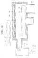
- FIG. 1Cis a schematic view showing constitutional elements of a conventional chemical vapor deposition apparatus in which the process gases are sequentially supplied and an external plasma generating apparatus is employed.
- the purge gascauses the source gases remaining in the showerhead 106 and the chamber 101 to be purged and discharged through the outlet 100 formed on a side of the chamber 101 .
- the plasma of the reactant gasesis injected through an external plasma generating apparatus 112 directly into the chamber 101 and the reactant gases are injected. Then, the reactant gases and the reaction byproduct gases are purged and discharged by using the purge gas.
- An object of the present inventionis to provide a chemical vapor deposition apparatus which uses radicals of reactant gases while supplying process gases in sequence by generating plasma within a showerhead or injecting exterior plasma into a chamber through the showerhead, thereby avoiding damage to a substrate and circuit elements formed on the substrate, ensuring a fast deposition rate even at low temperature, and depositing a thin film having excellent step coverage and film quality characteristics.
- Another object of the present inventionis to provide a chemical vapor deposition apparatus which effectively prevents source gases and reactant gases from being mixed with one another within a showerhead by partitioning the showerhead at a predetermined interval to divide it into two sections to separate a first section where the source gases are introduced and injected from a second section where the reactant gases are introduced and injected.
- a chemical vapor deposition apparatusincluding a chamber with an outlet formed at a lower portion thereof; a source gas introduction tube, a reactant gas introduction tube and a purge gas introduction tube for respectively supplying process gases into the chamber; a showerhead with a plurality of injection holes for injecting the process gases supplied through the introduction tubes; and a heater for supporting a wafer or substrate on which a thin film is deposited and for serving as a heat source,
- the apparatusbeing characterized in that an RF power source connection portion connectable to an external RF power source is installed on an upper side of the chamber; an RF electrode plate is installed within the chamber to be spaced by a predetermined gap from an inner upper surface of the chamber and to be spaced by a predetermined gap from the showerhead disposed below the RF electrode plate; the RF power source connection portion and the RF electrode plate are connected with each other through an RF rod so that electric power is supplied from the external RF power source to
- an RF power source connection portion connectable to an external RF power sourceis installed on an upper side of the chamber; an RF electrode plate is installed within the chamber to be spaced by a predetermined gap from an inner upper surface of the chamber and to be spaced by a predetermined gap from an upper surface of the showerhead disposed below the RF electrode plate; the RF power source connection portion and the RF electrode plate are connected with each other through an RF rod so that electric power is supplied from the external RF power source to the RF electrode plate; plasma is generated in a first buffer portion defined by a gap between the RF electrode plate and the upper surface of the showerhead, by means of the electric power applied from the external RF power source to the RF electrode plate; the showerhead is divided into two sections in a vertical direction and a second buffer portion is defined by a space between the two sections; reactant gases are supplied to the first buffer portion where the plasma is generated and are then injected onto the wafer or substrate through the showerhead; and source
- an external plasma generating apparatusis connected through a plasma guide tube to an upper side of the chamber to communicate with the chamber; a buffer portion is formed above the showerhead which is disposed below an inner upper surface of the chamber and spaced apart therefrom with a predetermined gap; plasma generated in the external plasma generating apparatus is introduced into the buffer portion through the plasma guide tube; and radicals of reactant gases thus generated are injected onto the wafer or substrate through the showerhead disposed below the buffer portion.
- an external plasma generating apparatusis connected through a plasma guide tube to an upper side of the chamber to communicate therewith; a first buffer portion is formed above the showerhead which is disposed below an upper surface of the chamber to spaced apart therefrom with a predetermined gap; the showerhead is divided into two sections in a vertical direction and a second buffer portion is defined by a space between the two sections; reactant gases and the plasma generated in the external plasma generating apparatus are supplied to the first buffer portion and are then injected onto the wafer or substrate through the showerhead; and source gases are supplied to the second buffer portion and then injected onto the wafer or substrate through the showerhead.
- an RF power source connection portion connectable to an external RF power sourceis installed on an inner upper side of the chamber; a first buffer portion is formed above the showerhead which is disposed below an upper surface of the chamber and spaced apart therefrom with a predetermined gap; the RF power source connection portion and an upper surface of the showerhead are connected with each other through an RF rod so that electric power is supplied from the external RF power source to the showerhead; the showerhead is divided into two sections in a vertical direction and a second buffer portion is defined by a space between the two sections; plasma is generated in the second buffer portion by means of the electric power applied from the RF power source to the showerhead and then injected onto the wafer or substrate through the showerhead; and source gases are supplied to the first buffer portion and then injected onto the wafer or substrate through the showerhead.
- FIG. 1Ais a schematic view showing constitutional elements of a conventional chemical vapor deposition apparatus in which process gases are sequentially supplied;
- FIG. 1Bis a schematic view showing constitutional elements of a conventional plasma chemical vapor deposition apparatus in which the process gases are sequentially supplied;
- FIG. 1Cis a schematic view showing constitutional elements of a conventional plasma chemical vapor deposition apparatus in which the process gases are sequentially supplied and an external plasma generating apparatus is employed;
- FIG. 2Ais a schematic view showing constitutional elements of a radical assisted chemical vapor deposition apparatus in which the process gases are sequentially supplied according to a first embodiment of the present invention
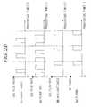
- FIG. 2Bis a graph showing a process of sequentially supplying the process gases and radicals of reactant gases by generating plasma within a showerhead of the chemical vapor deposition apparatus shown in FIG. 2A;
- FIG. 2Cis a graph showing a process of sequentially supplying the process gases and the radicals by generating the plasma within the showerhead of the chemical vapor deposition apparatus shown in FIG. 2A, in a state where a purge gas is always supplied;
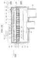
- FIG. 3Ais a schematic view showing constitutional elements of a radical assisted chemical vapor deposition apparatus in which the process gases are sequentially supplied and the plasma is generated in an upper portion of a showerhead partitioned at a predetermined interval according to a second embodiment of the present invention
- FIG. 3Bis a rear view showing a rear face of the showerhead which is an essential portion of the chemical vapor deposition apparatus shown in FIG. 3A;
- FIG. 4is a schematic view showing constitutional elements of a chemical vapor deposition apparatus in which the process gases are sequentially supplied and the external plasma generating apparatus is employed according to a third embodiment of the present invention
- FIG. 5is a schematic view showing constitutional elements of a radical assisted chemical vapor deposition apparatus in which the process gases are sequentially supplied and the external plasma generating apparatus is employed so that the plasma is introduced into the upper portion of the showerhead partitioned at the predetermined interval according to a fourth embodiment of the present invention
- FIG. 6Ais a schematic view showing constitutional elements of a radical assisted chemical vapor deposition apparatus in which the process gases are sequentially supplied and the plasma is generated in a lower portion of the showerhead partitioned at the predetermined interval according to a fifth embodiment of the present invention
- FIG. 6Bis a rear view showing a rear face of the showerhead which is an essential portion of the chemical vapor deposition apparatus shown in FIG. 6A;
- FIGS. 7 and 8are graphs showing processes of sequentially supplying the process gases and the radicals of the reactant gases in the chemical vapor deposition apparatus according to the present invention.
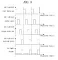
- FIGS. 9 and 10are graphs showing a process of sequentially supplying the process gases and the radicals of the reactant gases while maintaining a more stable state of the plasma in the chemical vapor deposition apparatus according to the present invention
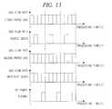
- FIG. 11is a graph showing a process of sequentially supplying the process gases and the radicals of the reactant gases while maintaining a more stable pressure of a chamber upon supply of source gases and reactant gases, which have difficulty in being deposited at a lower temperature, in the chemical vapor deposition apparatus according to the present invention.
- FIG. 12is a graph showing a process of sequentially supplying the process gases and the radicals of the reactant gases while maintaining a more stable pressure of the chamber and a more stable state of the plasma upon supply of source gases and reactant gases, which have difficulty in being deposited at a lower temperature and in a low energy plasma state, in the chemical vapor deposition apparatus according to the present invention.
- FIG. 2Ais a schematic view showing constitutional elements of a radical assisted chemical vapor deposition apparatus in which process gases are sequentially supplied according to a first embodiment of the present invention.
- the chemical vapor deposition apparatus of the present inventionis constructed such that a thin film is formed by sequential supply of process gases consisting of the processes of injecting and purging source gases and injecting and purging reactant gases, where the reactant gases are injected in a state where plasma is generated within a showerhead upon their injection.
- an upper plate 212is mounted on the top of a chamber 201 for constituting a portion of the chamber 201 , and an RF power source connection portion 209 which can be connected to an external RF power source 210 is installed on a side of the upper plate 212 .
- the RF power source connection portion 209is connected to an RF rod 211 , and the RF rod 211 is electrically insulated from the upper plate 212 by means of an RF rod insulation portion 213 formed around the RF rod 211 .
- the RF rod 211is connected to an RF electrode plate 214 installed on an inner side of the upper plate 212 , and plasma is generated within a showerhead 206 by means of such RF electrode plate 214 .
- an upper insulation portion 215is installed above the RF electrode plate 214 , i.e. between the RF electrode plate 214 and the upper plate 212 .
- a lower insulation portion 216is installed on the bottom of the RF electrode plate 214 in such a manner that a buffer portion 217 is defined with a predetermined gap between the RF electrode plate 214 and the showerhead 206 disposed below the RF electrode plate 214 by means of the lower insulation portion 216 . That is, the lower insulation portion 216 causes the RF electrode plate 214 to be insulated from an inner surface of the upper plate 212 and simultaneously to be spaced apart from the showerhead 206 disposed below the RF electrode plate 214 with a the predetermined gap.
- the showerhead 206is installed below the buffer portion having the predetermined gap defined by the lower insulation portion 216 , and is formed with a plurality of injection holes 205 for uniformly injecting the process gases. Further, the showerhead 206 is electrically grounded through connection with the upper plate 212 . In the chemical vapor deposition apparatus of the present invention constructed as such, the plasma is generated in the buffer portion 217 having the predetermined gap defined by the RF electrode plate 214 installed on the upper plate 212 , the lower insulation portion 216 and the showerhead 206 .
- a heater 208supports a wafer or substrate 207 (hereinafter, referred to as “substrate”) on which a thin film is actually formed and simultaneously supplies the substrate with predetermined thermal energy, within the chamber 201 which is disposed below the upper plate 212 and in which the supplied process gases react with one another.
- substratea wafer or substrate 207
- the upper plate 212On an outer side of the upper plate 212 are formed at least one source gas introduction tube 202 , at least one reactant gas introduction tube 203 and at least one purge gas introduction tube 204 , which communicate with the interior of the upper plate 212 . Further, a heater 218 for maintaining the upper plate 212 at a constant temperature is embedded in the upper plate 212 . That is, the temperature around the top of the chamber 201 can be kept constant by means of the heater 218 .
- the source gasesare introduced for a predetermined period of time through the at least one source gas introduction tube 202 formed on the outer side of the upper plate 212 and are injected through the showerhead 206 so that the source gases are adsorbed on the substrate 207 .
- the source gases remaining in the showerhead 206 and the chamber 201are purged and discharged for a predetermined period of time through an outlet 200 installed on a side of the chamber 201 by using a purge gas which is introduced through the at least purge gas introduction tube 204 installed on the outer side of the upper plate 212 .
- the reactant gaseswhich are introduced through the at least one reactant gas introduction tube 203 installed on the outer side of the upper plate 212 , are injected through the showerhead 206 onto the substrate 207 for a predetermined period of time so as to induce reactions of the injected reactant gases with the source gases adsorbed on the substrate 207 and to form the thin film on the substrate 207 .
- the reactions of the injected reactant gases with the source gases adsorbed on the substrate 207are further activated by applying electric power from the RF power source 210 to the RF electrode plate 214 to generate the plasma within the buffer portion 217 and injecting radicals of the reactant gases through the showerhead 206 .
- the reactant gases remaining in the showerhead 206 and the chamber 201are purged and discharged for a predetermined period of time by using the purge gas which is introduced through the purge gas introduction tube 204 .
- the present inventionallows the thin film to be formed on the wafer or substrate by repeating the sequential supply of the process gases consisting of the processes of injecting and purging the source gases, injecting the radicals of the reactant gases, and purging the reactant gases.
- the chemical vapor deposition apparatus of the present inventioncan ensure a fast deposition rate at a lower temperature and form a thin film having excellent step coverage and film quality characteristics on the substrate by further activating the reactions of the reactant gases with the source gases adsorbed on the wafer or substrate by means of the plasma generated in the buffer portion 217 .
- the chemical vapor deposition apparatus of the present inventionsince the plasma is not exposed directly to the chamber and the substrate, it is possible to prevent the substrate and circuit elements formed thereon from being physically damaged due to arc which may be produced during generation of the plasma, ion bombarding and ion implant.
- FIG. 2Bshows a graph diagrammatically illustrating the sequential supply of the process gases consisting of the processes of injecting and purging the source gases, injecting the radicals of the reactant gases, and purging the reactant gases while generating the plasma within the showerhead of the chemical vapor deposition apparatus shown in FIG. 2A.
- Inert gas atmosphereis first created in the showerhead and the chamber by injecting the purge gas through the showerhead for a predetermined period of time, as shown in FIG. 2B (ii). Then, the source gases are injected for a predetermined period of time to be adsorbed on the wafer or substrate, as shown in FIG. 2B (i). Subsequently, the source gases remaining in the showerhead and the chamber are purged and discharged by using the purge gas for the predetermined period of time, as shown in FIG. 2B (ii). Thereafter, as shown in FIGS.
- the reactant gasesare introduced into the showerhead for a predetermined period of time, and at the same time, the plasma is generated within the showerhead so that the radicals of the reactant gases are injected onto the wafer or substrate.
- the thin film having a predetermined thicknessis formed on the wafer or substrate by injecting the radicals of the reactant gases for the predetermined period of time in such a manner, the injection of the reactant gases and the electric power supplied from the RF power source to the RF electrode plate are cut off to extinguish the plasma. Then, the reactant gases and reaction byproduct gases remaining in the showerhead and the chamber are purged and discharged by using the purge gas. Accordingly, the thin film having the predetermined thickness is formed on the wafer or substrate by repeating such processes.
- FIG. 2Cis a graph showing a process of preventing mixing of the source gases with the reactant gases within the showerhead and the chamber by sequentially supplying only the source and reactant gases while continuously supplying the purge gas during sequential supply of the process gases and generating the plasma within the showerhead of the chemical vapor deposition apparatus shown in FIG. 2A.
- FIG. 3Ais a schematic view showing constitutional elements of a radical assisted chemical vapor deposition apparatus in which the process gases are sequentially supplied and the plasma is generated in an upper portion of a showerhead partitioned into a predetermined pattern according to a second embodiment of the present invention.
- the chemical vapor deposition apparatus of the present inventionis constructed such that a thin film is formed by sequentially supplying the process gases using the processes of injecting and purging the source gases and injecting and purging the reactant gases; that mixing of the source gases with the reactant gases is completely prevented within the showerhead by partitioning the showerhead into two sections to separate a first section where the source gases are introduced and injected from a second section where the reactant gases are introduced and injected; and that upon injection of the reactant gases, the radicals of the reactant gases can be injected by generating the plasma within a section of the showerhead into which the reactant gases are introduced and injected.
- an upper plate 301is mounted on the top of a chamber 300 for constituting a portion of the chamber 300 , and an RF power source connection portion 303 which can be connected to an external RF power source 302 is installed on a side of the upper plate 301 .
- the RF power source connection portion 303is connected to an RF rod 304 , and the RF rod 304 is electrically insulated from the upper plate 301 by means of an RF rod insulation portion 305 formed around the RF rod 304 .
- the RF rod 304is connected to an RF electrode plate 306 installed on an inner side of the upper plate 301 , and the plasma is generated within the showerhead by means of such RF electrode plate 306 .
- an upper insulation portion 307is installed above the RF electrode plate 306 , i.e., between the RF electrode plate 306 and the upper plate 301 .
- a lower insulation portion 308is installed on the bottom of the RF electrode plate 306 in such a manner that a first buffer portion 310 is defined with a predetermined gap between the RF electrode plate 306 and a first showerhead 309 disposed below the RF electrode plate 306 by means of the lower insulation portion 308 . That is, the lower insulation portion 308 causes the RF electrode plate 306 to be insulated from an inner surface of the upper plate 301 and simultaneously to be spaced apart from the first showerhead 309 disposed below the RF electrode plate 306 with the predetermined gap.
- the first showerhead 309is installed below the buffer portion having the predetermined gap defined by the lower insulation portion 308 , and is formed with a plurality of radical injection tubes 311 for uniformly injecting the radicals of the reactant gases. Further, the first showerhead 309 is electrically grounded through connection with the upper plate 301 .
- the plasmais generated in the first buffer portion 310 having the predetermined gap defined by the RF electrode plate 306 installed on the upper plate 301 , the lower insulation portion 308 and the first showerhead 309 .
- a lower plate 312 having a predetermined height, which constitutes a portion of the chamber 300is mounted on the bottom of the first showerhead 309 .
- a second showerhead 313is installed on a lower side of the lower plate 312 . That is, the first and second showerheads 309 , 313 are disposed to vertically face each other with a predetermined gap therebetween by means of the lower plate 312 .
- the second showerhead 313 thus disposedis formed with a plurality of through-holes 314 through which the plurality of radical injection tubes 311 formed in the first showerhead 309 penetrate and a plurality of source gas injection holes 315 for uniformly injecting the source gases.
- first and second showerheads 309 , 313 constructed as suchare disposed in places by fitting the radical injection tubes 311 of the first showerhead 309 into the through-holes 314 of the second showerhead 313 and forming the predetermined gap between the first and second showerheads 309 , 313 , a second buffer portion 316 is defined.
- the upper plate 301On an outer side of the upper plate 301 are installed at least one reactant gas introduction tube 317 and a first purge gas introduction tube 318 to penetrate through the upper plate 301 .
- the reactant gases and the purge gasare supplied to the first buffer portion 310 through the reactant gas introduction tube 317 and the first purge gas introduction tube 318 .
- the lower plate 312On an outer side of the lower plate 312 are installed at least one source gas introduction tube 319 and a second purge gas introduction tube 320 to penetrate through the lower plate 312 .
- the source gases and the purge gasare supplied to the second buffer portion 316 through the source gas introduction tube 319 and the second purge gas introduction tube 320 .
- a heater 323supports a wafer or substrate 322 (hereinafter, referred to as “substrate”) on which a thin film is actually formed and simultaneously supplies the substrate with predetermined thermal energy, within the chamber 300 which is disposed below the lower plate 312 and in which the supplied process gases react with one another. Further, another heater 321 for maintaining the upper plate 301 at a constant temperature is embedded in the upper plate 301 . That is, the temperature around the top of the chamber 300 can be kept constant by means of the heater 321 .
- FIG. 3Bis a rear view showing a rear face of the showerhead which is an essential portion of the chemical vapor deposition apparatus shown in FIG. 3A. Holes 325 of the plurality of radical injection tubes 311 and the source gas injection holes 315 are arranged in a grid pattern on the rear face of the second showerhead 313 .
- the source gasesare introduced into the second buffer portion 316 for a predetermined period of time through the source gas introduction tube 319 installed on the lower plate 312 and are injected through the source gas injection holes 315 formed in the second showerhead 313 so that the source gases are adsorbed on the substrate 322 .
- the source gases remaining in the second showerhead 313 and the chamber 300are purged and discharged for a predetermined period of time through an outlet 324 installed on a side of the chamber 300 by using the purge gas which is introduced through the second purge gas introduction tube 320 .
- the reactant gasesare supplied to the first buffer portion 310 for a predetermined period of time through the reactant gas introduction tube 317 installed on the upper plate 301 and are injected through the radical injection tubes 311 formed in the first showerhead 309 onto the substrate 322 so as to induce reactions of the injected reactant gases with the source gases adsorbed on the substrate 322 and to form the thin film on the substrate 322 .
- the reaction of the injected reactant gases with the source gases adsorbed on the substrate 322is further activated by applying electric power from the RF power source 302 to the RF electrode plate 306 to generate the plasma within the first buffer portion 310 and injecting the radicals of the reactant gases through the radical injection tubes 311 fitted into the through-holes 314 of the second showerhead 313 .
- the reactant gases remaining in the first showerhead 309 and the chamber 300are purged and discharged for a predetermined period of time by using the purge gas which is introduced through the first purge gas introduction tube 318 .
- the present inventionallows formation of the thin film having the predetermined thickness on the wafer or substrate by separately introducing the source gases and the reactant gases and by repeating the sequential supply of the process gases consisting of the processes of injecting and purging the source gases, injecting the radicals of the reactant gases, and purging the reactant gases.
- the chemical vapor deposition apparatus of the present inventioncan ensure a faster deposition rate and form a thin film having excellent step coverage and film quality characteristics on the wafer or substrate by further activating the reaction of the reactant gases with the source gases adsorbed on the wafer or substrate by means of the radicals of the reactant gases injected through the radical injection tubes 311 .
- the chemical vapor deposition apparatus of the present inventionsince the plasma is separated from the second showerhead 313 through which the source gases are injected, it is possible to thoroughly prevent the source gases, which have not been completely removed even by the purging process using the purge gas, from reacting with the plasma of the reactant gases within the showerhead and thus to avoid generation of particles and deterioration of the step coverage. Furthermore, according to the chemical vapor deposition apparatus of the present invention, since the chamber and the wafer or substrate are not directly exposed to the plasma, it is possible to prevent any physical damages to the wafer or substrate and circuit elements formed thereon due to arc which may be produced during generation of the plasma, ion bombarding and ion implant.
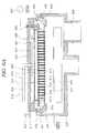
- FIG. 4is a schematic view showing constitutional elements of a chemical vapor deposition apparatus in which the process gases are sequentially supplied and an external plasma generating apparatus is employed according to a third embodiment of the present invention.
- the chemical vapor deposition apparatus of the present inventioncomprises a chamber 401 with an outlet 400 disposed at a lower portion thereof, a showerhead 406 with a plurality of injection holes 405 formed therein for injecting the process gases, and a heater 408 for supporting a wafer or substrate 407 (hereinafter, referred to as “substrate”) on which a thin film is deposited with the process gases injected through the showerhead 406 and for simultaneously functioning as a heat source.
- substratewafer or substrate 407
- An upper plate 409is mounted on the top of the chamber 401 for constituting a portion of the chamber 401 .
- An external plasma generating apparatus 410is connected with the chamber 401 to communicate with each other on an outer side of the upper plate 409 .
- At least one reactant gas introduction tube 403 and at least one purge gas introduction tube (second purge gas introduction tube) 404are installed on a side of the external plasma generating apparatus 410 to penetrate into the external plasma generating apparatus 410 , so that the plasma and radicals of the reactant gases can be generated upon creation of the plasma within the external plasma generating apparatus 410 .
- the plasma and radicals generated in the external plasma generating apparatus 410are introduced, through a plasma guide tube 411 formed to penetrate into a portion of the upper plate 409 , into a buffer portion 412 defined with a predetermined gap between the upper plate 409 and the showerhead 406 .
- a plasma guide tube 411formed to penetrate into a portion of the upper plate 409 , into a buffer portion 412 defined with a predetermined gap between the upper plate 409 and the showerhead 406 .
- an insulation portion 413should be installed in the plasma guide tube 411 to prevent the plasma and radicals from being extinguished until they reach the buffer portion 412 .
- a heater 415 for keeping the upper plate 409 at a constant temperatureis embedded in the upper plate 409 . The temperature around the top of the chamber 401 can be kept constant by means of the heater 415 .
- the chemical vapor deposition apparatus of the present inventionallows formation of the thin film having a predetermined thickness on the wafer or substrate using the process gases supplied through the introduction tubes and the external plasma generating apparatus by supplying the process gases in sequential processes of injecting and purging the source gases, injecting the radicals of the reactant gases, and purging the reactant gases.
- Inert gas atmosphereis first created in the showerhead 406 and the chamber 401 by introducing the purge gas through the second purge gas introduction tube 404 installed on the side of the external plasma generating apparatus 410 , the buffer portion 412 defined with the predetermined gap within the upper plate 409 , and the showerhead 406 disposed below the buffer portion 412 for a predetermined period of time. Then, the source gases are introduced through the source gas introduction tube 402 , which is installed at the portion on the side of the plasma guide tube 411 to penetrate thereinto, for a predetermined period of time to be adsorbed on the substrate 407 .
- the source gases remaining in the showerhead 406 and the chamber 401are purged and discharged by supplying the purge gas through the first purge gas introduction tube 414 , which is installed at the portion on the side of the plasma guide tube 414 to penetrate thereinto, for a predetermined period of time.
- the reactant gasesare introduced, through the reactant gas introduction tube 403 installed on the side of the external plasma generating apparatus 410 , into the external plasma generating apparatus 410 for a predetermined period of time.
- plasmais generated within the external plasma generating apparatus 410 , so that the plasma of the reactant gases is introduced into the buffer portion 412 through the plasma guide tube 411 and the radicals of the reactant gases are injected through the showerhead 406 onto the substrate 407 for a predetermined period of time.
- the thin film having a predetermined thicknessis formed on the substrate 407 by injecting the radicals of the reactant gases for the predetermined period of time in such a way. introduction of the reactant gases is cut off and the plasma in the external plasma generating apparatus 410 is extinguished. Then, the reactant gases and reaction byproduct gases remaining in the showerhead 406 and the chamber 401 are purged and discharged by introducing the purge gas through the second purge gas introduction tube 404 . Accordingly, the thin film having a predetermined thickness is formed on the wafer or substrate by repeating such processes.
- FIG. 5is a schematic view showing constitutional elements of a radical assisted chemical vapor deposition apparatus in which the process gases are supplied in a sequential manner and the external plasma generating apparatus is employed so that the plasma is introduced into an upper portion of the showerhead partitioned into a predetermined shape according to a fourth embodiment of the present invention.
- an upper plate 501is mounted on the top of a chamber 500 to constitute a portion of the chamber 500 .
- An external plasma generating apparatus 503is connected with the chamber 500 to communicate with each other on an outer side of the upper plate 501 .
- At least one reactant gas introduction tube 517 and a first purge gas introduction tube 518are installed on a side of the external plasma generating apparatus 503 to penetrate thereinto, so that the plasma and radicals of the reactant gases can be generated upon creation of the plasma within the external plasma generating apparatus 503 .
- the plasma and radicals generated in the external plasma generating apparatus 503are introduced, through a plasma guide tube 504 formed to penetrate into a portion of the upper plate 501 , into a buffer portion 510 defined with a predetermined gap between the upper plate 501 and a first showerhead 509 .
- an insulation portion 505is installed in the plasma guide tube 504 to prevent the plasma and radical from being extinguished until they reach the first buffer portion 510 .
- the first showerhead 509is installed below the first buffer portion 510 , and is formed with a plurality of radical injection tubes 511 for uniformly injecting the radicals of the reactant gases.
- a lower plate 512 having a predetermined height, which constitutes a portion of the chamber 500is mounted on the bottom of the first showerhead 509 .
- a second showerhead 513is installed on a lower side of the lower plate 512 . That is, the first and second showerheads 509 , 513 are disposed to vertically face each other with a predetermined gap therebetween by means of the lower plate 512 .
- the second showerhead 513 thus disposedis formed with a plurality of through-holes 514 through which the plurality of radical injection tubes 511 formed in the first showerhead 509 pass. Also, there are formed a plurality of source gas injection holes 515 for uniformly injecting the source gases.
- first and second showerheads 509 , 513 constructed as suchare disposed in places by fitting the radical injection tubes 511 of the first showerhead 509 into the through-holes 514 of the second showerhead 513 and forming the predetermined gap between the first and second showerheads 509 , 513 , a second buffer portion 516 is defined. Further, the second showerhead 513 is electrically grounded through connection with the lower plate 512 .
- the lower plate 512On an outer side of the lower plate 512 are installed at least one source gas introduction tube 519 and a second purge gas introduction tube 520 to penetrate through the lower plate 512 .
- the source gases and the purge gasare introduced into the second buffer portion 516 through the source gas introduction tube 519 and the second purge gas introduction tube 520 .
- a heater 523supports a wafer or substrate 522 (hereinafter, referred to as “substrate”) on which a thin film is actually formed.
- the heateralso supplies the substrate with predetermined thermal energy, within the chamber 500 which is disposed below the lower plate 512 and where the supplied process gases react with one another.
- another heater 521 for keeping the upper plate 501 at a constant temperatureis embedded in the upper plate 501 . That is, the temperature around the top of the chamber 500 can be kept constant by means of the heater 521 .
- the source gasesare introduced into the second buffer portion 516 for a predetermined period of time through the source gas introduction tube 519 installed on the lower plate 512 and are injected through the source gas injection holes 515 formed in the second showerhead 513 so that the source gases are adsorbed on the substrate 522 .
- the source gases remaining in the second showerhead 513 and the chamber 500are purged and discharged for a predetermined period of time through an outlet 524 installed on a side of the chamber 500 by using the purge gas which is introduced through the second purge gas introduction tube 520 .
- the reactant gasesare introduced, through the reactant gas introduction tube 517 installed on the side of the external plasma generating apparatus 503 , into the external plasma generating apparatus 503 for a predetermined period of time.
- plasmais generated within the external plasma generating apparatus 503 , and the plasma of the reactant gases is introduced into the first buffer portion 510 through the plasma guide tube 504 and the radicals of the reactant gases are injected through the radical injection tubes 511 of the first showerhead 509 onto the substrate 522 for a predetermined period of time.
- the reactant gases remaining in the first showerhead 509 and the chamber 500are purged and discharged for a predetermined period of time by using the purge gas being introduced through the first purge gas introduction tube 518 .
- the present inventionallows formation of the thin film having the predetermined thickness on the wafer or substrate by separately introducing the source gases and the reactant gases and by repeating the sequential supply of the process gases consisting of the processes of injecting and purging the source gases, injecting the radicals of the reactant gases, and purging the reactant gases.
- FIG. 6Ais a schematic view showing constitutional elements of a radical assisted chemical vapor deposition apparatus in which the process gases are sequentially supplied and the plasma is generated in a lower portion of the showerhead partitioned at the predetermined interval according to a fifth embodiment of the present invention.
- an upper plate 601is mounted on the top of a chamber 600 to constitute a portion of the chamber 600 , and an RF power source connection portion 603 which can be connected to an external RF power source 602 is installed on a side of the upper plate 601 .
- the RF power source connection portion 603is connected to an RF rod 604 , and the RF rod 604 is electrically insulated from the upper plate 601 by means of an RF rod insulation portion 605 formed around the RF rod 604 .
- the RF rod 604is connected to a first showerhead 609 installed on an inner side of the upper plate 601 .
- a first showerhead 609installed on an inner side of the upper plate 601 .
- an upper insulation portion 607is installed with a predetermined gap above the first showerhead 609 so as to make a close contact with an inner surface of the upper plate 601 .
- a lower insulation portion 608 having a predetermined heightwhich constitutes a portion of the chamber 600 , is installed on the bottom of the first showerhead 609 .
- a lower plate 612is mounted on an outer side of the lower insulation portion 608 .
- a second showerhead 613is installed below the lower insulation portion 608 and the lower plate 612 so that the first and second showerheads 609 , 613 are disposed to face each other with a predetermined gap therebetween.
- a second buffer portion 616 having a predetermined gapis defined by the first and second showerheads 609 , 613 .
- the second showerhead 613is electrically grounded through connection with the lower plate 612 .
- plasmais generated in the second buffer portion 616 having the predetermined gap, which is defined by the first showerhead 609 , the lower insulation portion 608 and the second showerhead 613 .
- An intermediate plate 606 with a plurality of injection holes for uniformly distributing the introduced source gases are formedis installed in the first buffer portion 610 .
- the intermediate plate 606is fixed to the first showerhead 609 by means of support pins 626 disposed below the intermediate plate 606 .
- the first showerhead 609is formed with a plurality of source gas injection tubes 611 for uniformly injecting the source gases.
- the second showerhead 613is formed with a plurality of through-holes 614 through which the plurality of source gas injection tubes 611 formed in the first showerhead 609 pass. There are also formed a plurality of radical injection holes 615 for uniformly injecting the radicals of the reactant gases generated by the plasma in the second buffer portion 616 .
- the first and second showerheads 609 , 613 constructed as suchare disposed in places by fitting the source gas injection tubes 611 of the first showerhead 609 into the through-holes 614 of the second showerhead 613 and forming the predetermined gap between the first and second showerheads 609 , 613 , the second buffer portion 616 is defined.
- the upper plate 601On an outer side of the upper plate 601 are installed at least one source gas introduction tube 619 and a first purge gas introduction tube 618 pass through the upper plate 601 .
- the source gases and the purge gasare supplied to the first buffer portion 610 through the source gas introduction tube 619 and the first purge gas introduction tube 618 .
- at least one reactant gas introduction tube 617 and a second purge gas introduction tube 620to penetrate through the upper plate 601 .
- the reactant gases and the purge gas, which have been introduced through the reactant gas introduction tube 617 and the second purge gas introduction tube 620 thus installed,are uniformly distributed through a circular reactant gas buffer portion 627 formed in the first showerhead 609 and then introduced through a reactant gas distribution hole 628 toward a reactant gas inlet 629 .
- the reactant gases and the purge gas, which have been introduced through the reactant gas inlet 629flow into the second buffer portion 616 .
- a heater 623supports a wafer or substrate 622 (hereinafter, referred to as “substrate”) on which a thin film is actually formed. Also, it supplies the substrate with predetermined thermal energy, within the chamber 600 which is disposed below the lower plate 612 and where the supplied process gases react with one another. Further, another heater 621 for keeping the upper plate 601 at a constant temperature is embedded in the upper plate 601 . That is, the temperature around the top of the chamber 600 can be kept constant by means of the heater 621 .
- FIG. 6Bis a rear view showing a rear face of the showerhead which is an essential portion of the chemical vapor deposition apparatus shown in FIG. 6A. Holes 6325 of the plurality of source gas injection tubes 611 and the radical injection holes 615 are arranged in a grid pattern on the rear face of the second showerhead 613 .
- the source gasesare introduced into the first buffer portion 610 for a predetermined period of time through the source gas introduction tube 619 installed on the upper plate 601 and are injected through the source gas injection tubes holes 611 formed in the first showerhead 609 so that the source gases are adsorbed on the substrate 622 .
- the source gases remaining in the first showerhead 609 and the chamber 600are purged and discharged for a predetermined period of time through an outlet 624 installed on a side of the chamber 600 by using the purge gas which is introduced through the first purge gas introduction tube 618 .
- the reactant gasesare supplied to the second buffer portion 616 for a predetermined period of time through the reactant gas introduction tube 617 installed on the upper plate 601 and are injected through the radical injection holes 615 formed in the second showerhead 613 onto the substrate 622 so as to induce reactions of the reactant gases with the source gases adsorbed on the substrate 622 and to form the thin film on the substrate 622 .
- the reactions of the reactant gases with the source gases adsorbed on the wafer or substrateare further activated by applying electric power from the RF power source 602 to the first showerhead 609 to generate the plasma within the second buffer portion 616 and injecting the radicals of the reactant gases through the radical injection holes 615 of the second showerhead 613 .
- the reactant gases and reaction byproduct gases remaining in the second showerhead 613 and the chamber 600are purged and discharged for a predetermined period of time by using the purge gas which is introduced through the second purge gas introduction tube 620 .
- the present inventionallows formation of the thin film having the predetermined thickness on the wafer or substrate by separately introducing the source gases and the reactant gases and by repeating the sequential supply of the process gases consisting of the processes of injecting and purging the source gases, injecting the radicals of the reactant gases, and purging the reactant gases.
- FIGS. 7 and 8are graphs diagrammatically illustrating the sequential supply of the process gases consisting of the processes of injecting and purging the source gases, injecting the radicals of the reactant gases, and purging the reactant gases in the chemical vapor deposition apparatus according to the present invention.
- the purge gasis injected through the first and second showerheads for the predetermined period of time to create the inert gas atmosphere within the showerhead and the chamber, and then, the source gases are injected for the predetermined period of time to cause the source gases to be adsorbed on the wafer or the substrate. Thereafter, the source gases remaining in the showerhead and the chamber are purged and discharged for the predetermined period of time by using the purge gas, and the reactant gases are then introduced into the showerhead for the predetermined period of time, and at the same time, the plasma is generated in the showerhead so as to inject the radicals of the reactant gases onto the wafer or substrate.
- the thin film having the predetermined thicknessis formed on the wafer or substrate by injecting the radicals of the reactant gases for the predetermined period of time.
- the introduction of the reactant gases and the electric power from the RF power source (or power source for the external plasma generating apparatus)are cut off to extinguish the plasma.
- the reactant gases and reaction byproduct gases remaining in the showerhead and the chamberare purged and discharged by using the purge gas.
- the thin film having the predetermined thicknessis formed on the wafer or the substrate.
- the reproducibility of the processescan be ensured by minimizing variations in the pressure of the chamber.
- FIGS. 9 and 10are graphs illustrating the sequential supply of the process gases consisting of the processes of injecting and purging the source gases, injecting the radicals of the reactant gases, and purging the reactant gases while maintaining a more stable state of the plasma in the chemical vapor deposition apparatus according to the present invention.
- FIG. 11is a graph diagrammatically illustrating the sequential supply of the process gases consisting of the processes of injecting and purging the source gases, injecting the radicals of the reactant gases, and purging the reactant gases while maintaining a more stable pressure of the chamber during supply of the source gases and the reactant gases in the chemical vapor deposition apparatus according to the present invention.
- One of major factors in determining the deposition rate of the chemical vapor deposition apparatus in which the process gases are sequentially suppliedis an adsorption ratio of the source gases with respect to the wafer or substrate.
- the reactant gasesare supplied even in a state where the plasma is not generated. In such a way, the adsorption ratio of the source gases can be improved.
- the deposition rate of the thin filmcan be enhanced by cutting off and purging the source gases, generating the plasma, and then forming the thin film by means of the radicals of the reactant gases using the reactant gases and the source gases adsorbed on the wafer or substrate.
- FIG. 12is a graph diagrammatically illustrating the sequential supply of the process gases consisting of the processes of injecting and purging the source gases, injecting the radicals of the reactant gases, and purging the reactant gases while stably maintaining the pressure of the chamber and the state of the plasma during the supply of the source gases and the reactant gases, which are not typically deposited at a lower temperature and in a low energy plasma state, in the chemical vapor deposition apparatus according to the present invention.
- the reactant gasesare continuously introduced during a process where the source gases do not react with the reactant gases at a low temperature, and during the state where the plasma generated in the showerhead is maintained by applying the electric power from the low RF power source (or low power source for the external plasma generating apparatus).
- the plasmahas a very low energy state.
- the plasma or radicalsare extinguished by the recombination phenomenon when they collide with the inner walls of the radical injection holes.
- the radicals of the reactant gasesare not introduced into the chamber. Even in a state where the reactant gases are continuously introduced and the plasma state is generated in the showerhead by means of the low electric power, the pressure of the chamber and the plasma state can be maintained more stably upon sequential supply of the process gases without affecting the process reaction.
- the chemical vapor deposition apparatus of the present inventioncan improve the low deposition rate that was a problem of a conventional chemical vapor deposition apparatus in which the process gases are sequentially supplied, and prevent the problems of the generation of plasma arc, the ion bombarding, the ion implant, and the like. In addition, it can prevent introduction of a large amount of particles and impurities such as C, H, Cl, Br, I and O which may be contained in the thin film deposited by the chemical vapor deposition method.
Landscapes
- Chemical & Material Sciences (AREA)
- Engineering & Computer Science (AREA)
- General Chemical & Material Sciences (AREA)
- Chemical Kinetics & Catalysis (AREA)
- Materials Engineering (AREA)
- Mechanical Engineering (AREA)
- Metallurgy (AREA)
- Organic Chemistry (AREA)
- Physics & Mathematics (AREA)
- Plasma & Fusion (AREA)
- Electromagnetism (AREA)
- Chemical Vapour Deposition (AREA)
Abstract
Description
- 1. Field of the Invention[0001]
- The present invention relates to a chemical vapor deposition (CVD) apparatus, and more particularly, to a chemical vapor deposition apparatus which uses radicals of reactant gases while supplying process gases in sequence by generating plasma within a showerhead or injecting exterior plasma into a chamber through the showerhead.[0002]
- 2. Description of the Prior Art[0003]
- Generally, in order to obtain excellent step coverage and film quality characteristics at low temperature, source gases and reactant gases are supplied to a chemical vapor deposition apparatus in sequence. Herein, a conventional chemical vapor deposition apparatus in which process gases are sequentially supplied will be briefly described with reference to FIGS. 1A to[0004]1C.
- FIG. 1A is a schematic view showing constitutional elements of the conventional chemical vapor deposition apparatus in which the process gases are sequentially supplied. As shown in FIG. 1A, the conventional chemical vapor deposition apparatus comprises a[0005]
chamber 101 with anoutlet 100 disposed at a lower portion thereof, at least one sourcegas introduction tube 102 mounted on a top surface of the chamber so as to penetrate into an inner central portion of thechamber 101, at least one reactantgas introduction tube 103 and at least one purgegas introduction tube 104, ashowerhead 106 with a plurality ofinjection holes 105 formed therein for injecting the process gases, and aheater 108 for supporting a wafer or substrate107 (hereinafter, referred to as “substrate”) on which a thin film is deposited from the process gases injected through theshowerhead 106 and for simultaneously functioning as a heat source. - In order to form the thin film on the[0006]
substrate 107 by using the conventional chemical vapor deposition apparatus constructed as such, the source gases introduced from the at least one sourcegas introduction tube 102 are injected through theshowerhead 106 for a predetermined period of time to be adsorbed by thesubstrate 107, and the purge gas is then introduced from the at least one purgegas introduction tube 104 for a predetermined period of time so as to purge the source gases remaining in theshowerhead 106 and thechamber 101. Subsequently, the gases are discharged through theoutlet 100. Thereafter, the reactant gases introduced through the at least one reactantgas introduction tube 103 are injected through theshowerhead 106 onto thesubstrate 107 for a predetermined period of time, and consequently, a thin film is formed on the substrate through the predetermined reaction of the reactant gases with source gases adsorbed in thesubstrate 107. Further, before the source gases are injected again, the reactant gases and reaction byproduct gases remaining in theshowerhead 106 and thechamber 101 are purged by using the purge gas for a predetermined period of time and then discharged. As described above, the thin film is deposited on thesubstrate 107 by repeating the processes of injecting and purging the source gases, and injecting and purging the reactant gases. - However, the technology using such a conventional chemical vapor deposition apparatus has a disadvantage of a very low deposition rate, and becomes a cause of increase in fabrication costs of a semiconductor when it is applied to a mass-production process of the semiconductor.[0007]
- FIG. 1B is a schematic view showing a conventional plasma chemical vapor deposition apparatus in which the process gases are sequentially supplied and which is constructed to make up for the disadvantages of the chemical vapor deposition apparatus shown in FIG. 1A. That is, as shown in FIG. 1B, the conventional plasma chemical vapor deposition apparatus is constructed in such a manner that the[0008]
showerhead 106 is provided with an RF powersource connection portion 109 which in turn is connected to an externalRF power source 110, and that aninsulating portion 111 for electrically insulating theshowerhead 106 to which theRF power source 110 has been connected is installed on theshowerhead 106, thereby generating the plasma directly within thechamber 101. - That is, although the plasma chemical vapor deposition apparatus shown in FIG. 1B has a conventional sequential process gas supply system in which the processes of injecting and purging the source gases, and injecting and purging the reactant gases are repeated in the same way as the chemical vapor deposition apparatus shown in FIG. 1A, it is constructed to ensure a fast reaction rate at a lower temperature by directly generating the plasma directly within the[0009]
chamber 101 upon injection of the reactant gases and inducing reactions of the plasma of the reactant gases with the source gases adsorbed in thesubstrate 107. - The direct plasma generating system shown in FIG. 1B ensures a slightly faster deposition rate at a relatively low temperature as compared with the system mentioned with reference to FIG. 1A. However, there is a disadvantage in that the substrate and circuit elements formed on the substrate may be damaged due to generation of arc at an initial stage of the plasma generation, ion bombarding and ion implant, and thus, the yield of the process is reduced.[0010]
- FIG. 1C is a schematic view showing constitutional elements of a conventional chemical vapor deposition apparatus in which the process gases are sequentially supplied and an external plasma generating apparatus is employed. After the source gases are injected through the[0011]
showerhead 106 for a predetermined period of time, the purge gas causes the source gases remaining in theshowerhead 106 and thechamber 101 to be purged and discharged through theoutlet 100 formed on a side of thechamber 101. After such purging of the source gases, the plasma of the reactant gases is injected through an externalplasma generating apparatus 112 directly into thechamber 101 and the reactant gases are injected. Then, the reactant gases and the reaction byproduct gases are purged and discharged by using the purge gas. - In such a case that the chemical vapor deposition apparatus having the external plasma generating apparatus is utilized, it is possible to somewhat reduce the damage caused to the substrate and the circuit elements formed on the substrate due to the plasma. However, there is a disadvantage in that a thin film cannot be uniformly deposited on a substrate having a large area due to non-uniformity of the plasma introduced directly into the chamber.[0012]
- An object of the present invention is to provide a chemical vapor deposition apparatus which uses radicals of reactant gases while supplying process gases in sequence by generating plasma within a showerhead or injecting exterior plasma into a chamber through the showerhead, thereby avoiding damage to a substrate and circuit elements formed on the substrate, ensuring a fast deposition rate even at low temperature, and depositing a thin film having excellent step coverage and film quality characteristics.[0013]
- Another object of the present invention is to provide a chemical vapor deposition apparatus which effectively prevents source gases and reactant gases from being mixed with one another within a showerhead by partitioning the showerhead at a predetermined interval to divide it into two sections to separate a first section where the source gases are introduced and injected from a second section where the reactant gases are introduced and injected.[0014]
- According to a first embodiment of the present invention for achieving the above objects, there is provided a chemical vapor deposition apparatus including a chamber with an outlet formed at a lower portion thereof; a source gas introduction tube, a reactant gas introduction tube and a purge gas introduction tube for respectively supplying process gases into the chamber; a showerhead with a plurality of injection holes for injecting the process gases supplied through the introduction tubes; and a heater for supporting a wafer or substrate on which a thin film is deposited and for serving as a heat source, the apparatus being characterized in that an RF power source connection portion connectable to an external RF power source is installed on an upper side of the chamber; an RF electrode plate is installed within the chamber to be spaced by a predetermined gap from an inner upper surface of the chamber and to be spaced by a predetermined gap from the showerhead disposed below the RF electrode plate; the RF power source connection portion and the RF electrode plate are connected with each other through an RF rod so that electric power is supplied from the external RF power source to the RF electrode plate; plasma is generated in a buffer portion defined by a gap between the RF electrode plate and the showerhead, by means of the electric power applied from the external RF power source to the RF electrode plate; and radicals of reactant gases thus generated are injected onto the wafer or substrate through the showerhead disposed below the buffer portion.[0015]
- Further, according to a second embodiment of the present invention, an RF power source connection portion connectable to an external RF power source is installed on an upper side of the chamber; an RF electrode plate is installed within the chamber to be spaced by a predetermined gap from an inner upper surface of the chamber and to be spaced by a predetermined gap from an upper surface of the showerhead disposed below the RF electrode plate; the RF power source connection portion and the RF electrode plate are connected with each other through an RF rod so that electric power is supplied from the external RF power source to the RF electrode plate; plasma is generated in a first buffer portion defined by a gap between the RF electrode plate and the upper surface of the showerhead, by means of the electric power applied from the external RF power source to the RF electrode plate; the showerhead is divided into two sections in a vertical direction and a second buffer portion is defined by a space between the two sections; reactant gases are supplied to the first buffer portion where the plasma is generated and are then injected onto the wafer or substrate through the showerhead; and source gases are supplied to the second buffer portion and then injected onto the wafer or substrate through the showerhead.[0016]
- Moreover, according to a third embodiment of the present invention, an external plasma generating apparatus is connected through a plasma guide tube to an upper side of the chamber to communicate with the chamber; a buffer portion is formed above the showerhead which is disposed below an inner upper surface of the chamber and spaced apart therefrom with a predetermined gap; plasma generated in the external plasma generating apparatus is introduced into the buffer portion through the plasma guide tube; and radicals of reactant gases thus generated are injected onto the wafer or substrate through the showerhead disposed below the buffer portion.[0017]
- Furthermore, according to a fourth embodiment of the present invention, an external plasma generating apparatus is connected through a plasma guide tube to an upper side of the chamber to communicate therewith; a first buffer portion is formed above the showerhead which is disposed below an upper surface of the chamber to spaced apart therefrom with a predetermined gap; the showerhead is divided into two sections in a vertical direction and a second buffer portion is defined by a space between the two sections; reactant gases and the plasma generated in the external plasma generating apparatus are supplied to the first buffer portion and are then injected onto the wafer or substrate through the showerhead; and source gases are supplied to the second buffer portion and then injected onto the wafer or substrate through the showerhead.[0018]
- In addition, according to a fifth embodiment of the present invention, an RF power source connection portion connectable to an external RF power source is installed on an inner upper side of the chamber; a first buffer portion is formed above the showerhead which is disposed below an upper surface of the chamber and spaced apart therefrom with a predetermined gap; the RF power source connection portion and an upper surface of the showerhead are connected with each other through an RF rod so that electric power is supplied from the external RF power source to the showerhead; the showerhead is divided into two sections in a vertical direction and a second buffer portion is defined by a space between the two sections; plasma is generated in the second buffer portion by means of the electric power applied from the RF power source to the showerhead and then injected onto the wafer or substrate through the showerhead; and source gases are supplied to the first buffer portion and then injected onto the wafer or substrate through the showerhead.[0019]
- The above and other objects, features and advantages of the invention will become more apparent from reading the following description of preferred embodiments taken in connection with the accompanying drawings in which:[0020]
- FIG. 1A is a schematic view showing constitutional elements of a conventional chemical vapor deposition apparatus in which process gases are sequentially supplied;[0021]
- FIG. 1B is a schematic view showing constitutional elements of a conventional plasma chemical vapor deposition apparatus in which the process gases are sequentially supplied;[0022]
- FIG. 1C is a schematic view showing constitutional elements of a conventional plasma chemical vapor deposition apparatus in which the process gases are sequentially supplied and an external plasma generating apparatus is employed;[0023]
- FIG. 2A is a schematic view showing constitutional elements of a radical assisted chemical vapor deposition apparatus in which the process gases are sequentially supplied according to a first embodiment of the present invention;[0024]
- FIG. 2B is a graph showing a process of sequentially supplying the process gases and radicals of reactant gases by generating plasma within a showerhead of the chemical vapor deposition apparatus shown in FIG. 2A;[0025]
- FIG. 2C is a graph showing a process of sequentially supplying the process gases and the radicals by generating the plasma within the showerhead of the chemical vapor deposition apparatus shown in FIG. 2A, in a state where a purge gas is always supplied;[0026]
- FIG. 3A is a schematic view showing constitutional elements of a radical assisted chemical vapor deposition apparatus in which the process gases are sequentially supplied and the plasma is generated in an upper portion of a showerhead partitioned at a predetermined interval according to a second embodiment of the present invention;[0027]
- FIG. 3B is a rear view showing a rear face of the showerhead which is an essential portion of the chemical vapor deposition apparatus shown in FIG. 3A;[0028]
- FIG. 4 is a schematic view showing constitutional elements of a chemical vapor deposition apparatus in which the process gases are sequentially supplied and the external plasma generating apparatus is employed according to a third embodiment of the present invention;[0029]
- FIG. 5 is a schematic view showing constitutional elements of a radical assisted chemical vapor deposition apparatus in which the process gases are sequentially supplied and the external plasma generating apparatus is employed so that the plasma is introduced into the upper portion of the showerhead partitioned at the predetermined interval according to a fourth embodiment of the present invention;[0030]
- FIG. 6A is a schematic view showing constitutional elements of a radical assisted chemical vapor deposition apparatus in which the process gases are sequentially supplied and the plasma is generated in a lower portion of the showerhead partitioned at the predetermined interval according to a fifth embodiment of the present invention;[0031]
- FIG. 6B is a rear view showing a rear face of the showerhead which is an essential portion of the chemical vapor deposition apparatus shown in FIG. 6A;[0032]
- FIGS. 7 and 8 are graphs showing processes of sequentially supplying the process gases and the radicals of the reactant gases in the chemical vapor deposition apparatus according to the present invention;[0033]
- FIGS. 9 and 10 are graphs showing a process of sequentially supplying the process gases and the radicals of the reactant gases while maintaining a more stable state of the plasma in the chemical vapor deposition apparatus according to the present invention;[0034]
- FIG. 11 is a graph showing a process of sequentially supplying the process gases and the radicals of the reactant gases while maintaining a more stable pressure of a chamber upon supply of source gases and reactant gases, which have difficulty in being deposited at a lower temperature, in the chemical vapor deposition apparatus according to the present invention; and[0035]
- FIG. 12 is a graph showing a process of sequentially supplying the process gases and the radicals of the reactant gases while maintaining a more stable pressure of the chamber and a more stable state of the plasma upon supply of source gases and reactant gases, which have difficulty in being deposited at a lower temperature and in a low energy plasma state, in the chemical vapor deposition apparatus according to the present invention.[0036]
- Hereinafter, chemical vapor deposition apparatuses according to preferred embodiments of the present invention will be described in detail with reference to the accompanying drawings.[0037]
- <First Embodiment>[0038]
- FIG. 2A is a schematic view showing constitutional elements of a radical assisted chemical vapor deposition apparatus in which process gases are sequentially supplied according to a first embodiment of the present invention.[0039]
- As can be seen in this figure, the chemical vapor deposition apparatus of the present invention is constructed such that a thin film is formed by sequential supply of process gases consisting of the processes of injecting and purging source gases and injecting and purging reactant gases, where the reactant gases are injected in a state where plasma is generated within a showerhead upon their injection.[0040]
- As shown in FIG. 2A, in the chemical vapor deposition apparatus of the present invention, an[0041]
upper plate 212 is mounted on the top of achamber 201 for constituting a portion of thechamber 201, and an RF powersource connection portion 209 which can be connected to an externalRF power source 210 is installed on a side of theupper plate 212. The RF powersource connection portion 209 is connected to anRF rod 211, and theRF rod 211 is electrically insulated from theupper plate 212 by means of an RFrod insulation portion 213 formed around theRF rod 211. - The[0042]
RF rod 211 is connected to anRF electrode plate 214 installed on an inner side of theupper plate 212, and plasma is generated within ashowerhead 206 by means of suchRF electrode plate 214. At this time, in order to electrically insulate theRF electrode plate 214, anupper insulation portion 215 is installed above theRF electrode plate 214, i.e. between theRF electrode plate 214 and theupper plate 212. Further, alower insulation portion 216 is installed on the bottom of theRF electrode plate 214 in such a manner that abuffer portion 217 is defined with a predetermined gap between theRF electrode plate 214 and theshowerhead 206 disposed below theRF electrode plate 214 by means of thelower insulation portion 216. That is, thelower insulation portion 216 causes theRF electrode plate 214 to be insulated from an inner surface of theupper plate 212 and simultaneously to be spaced apart from theshowerhead 206 disposed below theRF electrode plate 214 with a the predetermined gap. - The[0043]
showerhead 206 is installed below the buffer portion having the predetermined gap defined by thelower insulation portion 216, and is formed with a plurality of injection holes205 for uniformly injecting the process gases. Further, theshowerhead 206 is electrically grounded through connection with theupper plate 212. In the chemical vapor deposition apparatus of the present invention constructed as such, the plasma is generated in thebuffer portion 217 having the predetermined gap defined by theRF electrode plate 214 installed on theupper plate 212, thelower insulation portion 216 and theshowerhead 206. - A[0044]
heater 208 supports a wafer or substrate207 (hereinafter, referred to as “substrate”) on which a thin film is actually formed and simultaneously supplies the substrate with predetermined thermal energy, within thechamber 201 which is disposed below theupper plate 212 and in which the supplied process gases react with one another. - On an outer side of the[0045]
upper plate 212 are formed at least one sourcegas introduction tube 202, at least one reactantgas introduction tube 203 and at least one purgegas introduction tube 204, which communicate with the interior of theupper plate 212. Further, aheater 218 for maintaining theupper plate 212 at a constant temperature is embedded in theupper plate 212. That is, the temperature around the top of thechamber 201 can be kept constant by means of theheater 218. - Hereinafter, a process of forming the thin film on the substrate by using the chemical vapor deposition apparatus of the present invention constructed as mentioned above will be described in detail.[0046]
- The source gases are introduced for a predetermined period of time through the at least one source[0047]
gas introduction tube 202 formed on the outer side of theupper plate 212 and are injected through theshowerhead 206 so that the source gases are adsorbed on thesubstrate 207. After such injection of the source gases for the predetermined period of time, the source gases remaining in theshowerhead 206 and thechamber 201 are purged and discharged for a predetermined period of time through anoutlet 200 installed on a side of thechamber 201 by using a purge gas which is introduced through the at least purgegas introduction tube 204 installed on the outer side of theupper plate 212. - Then, the reactant gases, which are introduced through the at least one reactant[0048]
gas introduction tube 203 installed on the outer side of theupper plate 212, are injected through theshowerhead 206 onto thesubstrate 207 for a predetermined period of time so as to induce reactions of the injected reactant gases with the source gases adsorbed on thesubstrate 207 and to form the thin film on thesubstrate 207. At this time, the reactions of the injected reactant gases with the source gases adsorbed on thesubstrate 207 are further activated by applying electric power from theRF power source 210 to theRF electrode plate 214 to generate the plasma within thebuffer portion 217 and injecting radicals of the reactant gases through theshowerhead 206. - After injecting the radicals of the reactant gases for the predetermined period of time, the reactant gases remaining in the[0049]
showerhead 206 and thechamber 201 are purged and discharged for a predetermined period of time by using the purge gas which is introduced through the purgegas introduction tube 204. Thus, the present invention allows the thin film to be formed on the wafer or substrate by repeating the sequential supply of the process gases consisting of the processes of injecting and purging the source gases, injecting the radicals of the reactant gases, and purging the reactant gases. - In such a way, the chemical vapor deposition apparatus of the present invention can ensure a fast deposition rate at a lower temperature and form a thin film having excellent step coverage and film quality characteristics on the substrate by further activating the reactions of the reactant gases with the source gases adsorbed on the wafer or substrate by means of the plasma generated in the[0050]
buffer portion 217. Moreover, according to the chemical vapor deposition apparatus of the present invention, since the plasma is not exposed directly to the chamber and the substrate, it is possible to prevent the substrate and circuit elements formed thereon from being physically damaged due to arc which may be produced during generation of the plasma, ion bombarding and ion implant. - FIG. 2B shows a graph diagrammatically illustrating the sequential supply of the process gases consisting of the processes of injecting and purging the source gases, injecting the radicals of the reactant gases, and purging the reactant gases while generating the plasma within the showerhead of the chemical vapor deposition apparatus shown in FIG. 2A.[0051]
- Inert gas atmosphere is first created in the showerhead and the chamber by injecting the purge gas through the showerhead for a predetermined period of time, as shown in FIG. 2B (ii). Then, the source gases are injected for a predetermined period of time to be adsorbed on the wafer or substrate, as shown in FIG. 2B (i). Subsequently, the source gases remaining in the showerhead and the chamber are purged and discharged by using the purge gas for the predetermined period of time, as shown in FIG. 2B (ii). Thereafter, as shown in FIGS. 2[0052]b(c) and (d), the reactant gases are introduced into the showerhead for a predetermined period of time, and at the same time, the plasma is generated within the showerhead so that the radicals of the reactant gases are injected onto the wafer or substrate. After the thin film having a predetermined thickness is formed on the wafer or substrate by injecting the radicals of the reactant gases for the predetermined period of time in such a manner, the injection of the reactant gases and the electric power supplied from the RF power source to the RF electrode plate are cut off to extinguish the plasma. Then, the reactant gases and reaction byproduct gases remaining in the showerhead and the chamber are purged and discharged by using the purge gas. Accordingly, the thin film having the predetermined thickness is formed on the wafer or substrate by repeating such processes.
- FIG. 2C is a graph showing a process of preventing mixing of the source gases with the reactant gases within the showerhead and the chamber by sequentially supplying only the source and reactant gases while continuously supplying the purge gas during sequential supply of the process gases and generating the plasma within the showerhead of the chemical vapor deposition apparatus shown in FIG. 2A.[0053]
- When the purge gas is continuously supplied and only the source and reactant gases are sequentially supplied as shown in FIG. 2C, it is possible to minimize a variation in pressure of the chamber so that reproducibility of the processes can be improved.[0054]
- <Second Embodiment>[0055]
- FIG. 3A is a schematic view showing constitutional elements of a radical assisted chemical vapor deposition apparatus in which the process gases are sequentially supplied and the plasma is generated in an upper portion of a showerhead partitioned into a predetermined pattern according to a second embodiment of the present invention.[0056]
- As can be seen from this figure, the chemical vapor deposition apparatus of the present invention is constructed such that a thin film is formed by sequentially supplying the process gases using the processes of injecting and purging the source gases and injecting and purging the reactant gases; that mixing of the source gases with the reactant gases is completely prevented within the showerhead by partitioning the showerhead into two sections to separate a first section where the source gases are introduced and injected from a second section where the reactant gases are introduced and injected; and that upon injection of the reactant gases, the radicals of the reactant gases can be injected by generating the plasma within a section of the showerhead into which the reactant gases are introduced and injected.[0057]
- As shown in FIG. 3A, in the chemical vapor deposition apparatus of the present invention, an[0058]
upper plate 301 is mounted on the top of achamber 300 for constituting a portion of thechamber 300, and an RF powersource connection portion 303 which can be connected to an externalRF power source 302 is installed on a side of theupper plate 301. The RF powersource connection portion 303 is connected to anRF rod 304, and theRF rod 304 is electrically insulated from theupper plate 301 by means of an RFrod insulation portion 305 formed around theRF rod 304. - The[0059]
RF rod 304 is connected to anRF electrode plate 306 installed on an inner side of theupper plate 301, and the plasma is generated within the showerhead by means of suchRF electrode plate 306. At this time, in order to electrically insulate theRF electrode plate 306, an upper insulation portion307 is installed above theRF electrode plate 306, i.e., between theRF electrode plate 306 and theupper plate 301. Further, alower insulation portion 308 is installed on the bottom of theRF electrode plate 306 in such a manner that afirst buffer portion 310 is defined with a predetermined gap between theRF electrode plate 306 and afirst showerhead 309 disposed below theRF electrode plate 306 by means of thelower insulation portion 308. That is, thelower insulation portion 308 causes theRF electrode plate 306 to be insulated from an inner surface of theupper plate 301 and simultaneously to be spaced apart from thefirst showerhead 309 disposed below theRF electrode plate 306 with the predetermined gap. - The[0060]
first showerhead 309 is installed below the buffer portion having the predetermined gap defined by thelower insulation portion 308, and is formed with a plurality ofradical injection tubes 311 for uniformly injecting the radicals of the reactant gases. Further, thefirst showerhead 309 is electrically grounded through connection with theupper plate 301. - In the chemical vapor deposition apparatus of the present invention constructed as such, the plasma is generated in the[0061]
first buffer portion 310 having the predetermined gap defined by theRF electrode plate 306 installed on theupper plate 301, thelower insulation portion 308 and thefirst showerhead 309. - Moreover, a[0062]
lower plate 312 having a predetermined height, which constitutes a portion of thechamber 300, is mounted on the bottom of thefirst showerhead 309. Asecond showerhead 313 is installed on a lower side of thelower plate 312. That is, the first andsecond showerheads lower plate 312. Thesecond showerhead 313 thus disposed is formed with a plurality of through-holes 314 through which the plurality ofradical injection tubes 311 formed in thefirst showerhead 309 penetrate and a plurality of source gas injection holes315 for uniformly injecting the source gases. When the first andsecond showerheads radical injection tubes 311 of thefirst showerhead 309 into the through-holes 314 of thesecond showerhead 313 and forming the predetermined gap between the first andsecond showerheads second buffer portion 316 is defined. - Further, on an outer side of the[0063]
upper plate 301 are installed at least one reactantgas introduction tube 317 and a first purgegas introduction tube 318 to penetrate through theupper plate 301. The reactant gases and the purge gas are supplied to thefirst buffer portion 310 through the reactantgas introduction tube 317 and the first purgegas introduction tube 318. In addition, on an outer side of thelower plate 312 are installed at least one sourcegas introduction tube 319 and a second purgegas introduction tube 320 to penetrate through thelower plate 312. The source gases and the purge gas are supplied to thesecond buffer portion 316 through the sourcegas introduction tube 319 and the second purgegas introduction tube 320. - A[0064]
heater 323 supports a wafer or substrate322 (hereinafter, referred to as “substrate”) on which a thin film is actually formed and simultaneously supplies the substrate with predetermined thermal energy, within thechamber 300 which is disposed below thelower plate 312 and in which the supplied process gases react with one another. Further, anotherheater 321 for maintaining theupper plate 301 at a constant temperature is embedded in theupper plate 301. That is, the temperature around the top of thechamber 300 can be kept constant by means of theheater 321. - FIG. 3B is a rear view showing a rear face of the showerhead which is an essential portion of the chemical vapor deposition apparatus shown in FIG. 3A.[0065]
Holes 325 of the plurality ofradical injection tubes 311 and the source gas injection holes315 are arranged in a grid pattern on the rear face of thesecond showerhead 313. - Hereinafter, a process of forming the thin film on the substrate by using the chemical vapor deposition apparatus of the present invention constructed as mentioned above will be described in detail.[0066]
- The source gases are introduced into the[0067]
second buffer portion 316 for a predetermined period of time through the sourcegas introduction tube 319 installed on thelower plate 312 and are injected through the source gas injection holes315 formed in thesecond showerhead 313 so that the source gases are adsorbed on thesubstrate 322. After such injection of the source gases for the predetermined period of time, the source gases remaining in thesecond showerhead 313 and thechamber 300 are purged and discharged for a predetermined period of time through anoutlet 324 installed on a side of thechamber 300 by using the purge gas which is introduced through the second purgegas introduction tube 320. After discharging the remaining source gases in such a way, the reactant gases are supplied to thefirst buffer portion 310 for a predetermined period of time through the reactantgas introduction tube 317 installed on theupper plate 301 and are injected through theradical injection tubes 311 formed in thefirst showerhead 309 onto thesubstrate 322 so as to induce reactions of the injected reactant gases with the source gases adsorbed on thesubstrate 322 and to form the thin film on thesubstrate 322. At this time, the reaction of the injected reactant gases with the source gases adsorbed on thesubstrate 322 is further activated by applying electric power from theRF power source 302 to theRF electrode plate 306 to generate the plasma within thefirst buffer portion 310 and injecting the radicals of the reactant gases through theradical injection tubes 311 fitted into the through-holes 314 of thesecond showerhead 313. - After injecting the radicals of the reactant gases for the predetermined period of time, the reactant gases remaining in the[0068]
first showerhead 309 and thechamber 300 are purged and discharged for a predetermined period of time by using the purge gas which is introduced through the first purgegas introduction tube 318. Thus, the present invention allows formation of the thin film having the predetermined thickness on the wafer or substrate by separately introducing the source gases and the reactant gases and by repeating the sequential supply of the process gases consisting of the processes of injecting and purging the source gases, injecting the radicals of the reactant gases, and purging the reactant gases. - In such a way, the chemical vapor deposition apparatus of the present invention can ensure a faster deposition rate and form a thin film having excellent step coverage and film quality characteristics on the wafer or substrate by further activating the reaction of the reactant gases with the source gases adsorbed on the wafer or substrate by means of the radicals of the reactant gases injected through the[0069]
radical injection tubes 311. Moreover, according to the chemical vapor deposition apparatus of the present invention, since the plasma is separated from thesecond showerhead 313 through which the source gases are injected, it is possible to thoroughly prevent the source gases, which have not been completely removed even by the purging process using the purge gas, from reacting with the plasma of the reactant gases within the showerhead and thus to avoid generation of particles and deterioration of the step coverage. Furthermore, according to the chemical vapor deposition apparatus of the present invention, since the chamber and the wafer or substrate are not directly exposed to the plasma, it is possible to prevent any physical damages to the wafer or substrate and circuit elements formed thereon due to arc which may be produced during generation of the plasma, ion bombarding and ion implant. - <Third Embodiment>[0070]
- FIG. 4 is a schematic view showing constitutional elements of a chemical vapor deposition apparatus in which the process gases are sequentially supplied and an external plasma generating apparatus is employed according to a third embodiment of the present invention.[0071]
- As shown in this figure, the chemical vapor deposition apparatus of the present invention comprises a[0072]
chamber 401 with anoutlet 400 disposed at a lower portion thereof, ashowerhead 406 with a plurality of injection holes405 formed therein for injecting the process gases, and aheater 408 for supporting a wafer or substrate407 (hereinafter, referred to as “substrate”) on which a thin film is deposited with the process gases injected through theshowerhead 406 and for simultaneously functioning as a heat source. - An[0073]
upper plate 409 is mounted on the top of thechamber 401 for constituting a portion of thechamber 401. An externalplasma generating apparatus 410 is connected with thechamber 401 to communicate with each other on an outer side of theupper plate 409. At least one reactantgas introduction tube 403 and at least one purge gas introduction tube (second purge gas introduction tube)404 are installed on a side of the externalplasma generating apparatus 410 to penetrate into the externalplasma generating apparatus 410, so that the plasma and radicals of the reactant gases can be generated upon creation of the plasma within the externalplasma generating apparatus 410. - The plasma and radicals generated in the external[0074]
plasma generating apparatus 410 are introduced, through aplasma guide tube 411 formed to penetrate into a portion of theupper plate 409, into abuffer portion 412 defined with a predetermined gap between theupper plate 409 and theshowerhead 406. At this time, since the plasma and radicals generated in the externalplasma generating apparatus 410 are extinguished due to a phenomenon of recombination when they collide against a conductor, aninsulation portion 413 should be installed in theplasma guide tube 411 to prevent the plasma and radicals from being extinguished until they reach thebuffer portion 412. - Further, at least one source[0075]
gas introduction tube 402 and at least one purge gas introduction tube (first purge gas introduction tube)414 communicate with a portion on a side of theplasma guide tube 411. In addition, aheater 415 for keeping theupper plate 409 at a constant temperature is embedded in theupper plate 409. The temperature around the top of thechamber 401 can be kept constant by means of theheater 415. - That is, the chemical vapor deposition apparatus of the present invention allows formation of the thin film having a predetermined thickness on the wafer or substrate using the process gases supplied through the introduction tubes and the external plasma generating apparatus by supplying the process gases in sequential processes of injecting and purging the source gases, injecting the radicals of the reactant gases, and purging the reactant gases.[0076]
- Hereinafter, a process of forming the thin film on the substrate by using the chemical vapor deposition apparatus of the present invention constructed as mentioned above will be described in detail.[0077]
- Inert gas atmosphere is first created in the[0078]
showerhead 406 and thechamber 401 by introducing the purge gas through the second purgegas introduction tube 404 installed on the side of the externalplasma generating apparatus 410, thebuffer portion 412 defined with the predetermined gap within theupper plate 409, and theshowerhead 406 disposed below thebuffer portion 412 for a predetermined period of time. Then, the source gases are introduced through the sourcegas introduction tube 402, which is installed at the portion on the side of theplasma guide tube 411 to penetrate thereinto, for a predetermined period of time to be adsorbed on thesubstrate 407. Subsequently, the source gases remaining in theshowerhead 406 and thechamber 401 are purged and discharged by supplying the purge gas through the first purgegas introduction tube 414, which is installed at the portion on the side of theplasma guide tube 414 to penetrate thereinto, for a predetermined period of time. - Then, the reactant gases are introduced, through the reactant[0079]
gas introduction tube 403 installed on the side of the externalplasma generating apparatus 410, into the externalplasma generating apparatus 410 for a predetermined period of time. At the same time, plasma is generated within the externalplasma generating apparatus 410, so that the plasma of the reactant gases is introduced into thebuffer portion 412 through theplasma guide tube 411 and the radicals of the reactant gases are injected through theshowerhead 406 onto thesubstrate 407 for a predetermined period of time. After forming the thin film having a predetermined thickness on thesubstrate 407 by injecting the radicals of the reactant gases for the predetermined period of time in such a way, introduction of the reactant gases is cut off and the plasma in the externalplasma generating apparatus 410 is extinguished. Then, the reactant gases and reaction byproduct gases remaining in theshowerhead 406 and thechamber 401 are purged and discharged by introducing the purge gas through the second purgegas introduction tube 404. Accordingly, the thin film having a predetermined thickness is formed on the wafer or substrate by repeating such processes. - <Fourth Embodiment>[0080]
- FIG. 5 is a schematic view showing constitutional elements of a radical assisted chemical vapor deposition apparatus in which the process gases are supplied in a sequential manner and the external plasma generating apparatus is employed so that the plasma is introduced into an upper portion of the showerhead partitioned into a predetermined shape according to a fourth embodiment of the present invention.[0081]
- As shown in this figure, in the chemical vapor deposition apparatus of the present invention, an[0082]
upper plate 501 is mounted on the top of achamber 500 to constitute a portion of thechamber 500. An externalplasma generating apparatus 503 is connected with thechamber 500 to communicate with each other on an outer side of theupper plate 501. At least one reactantgas introduction tube 517 and a first purgegas introduction tube 518 are installed on a side of the externalplasma generating apparatus 503 to penetrate thereinto, so that the plasma and radicals of the reactant gases can be generated upon creation of the plasma within the externalplasma generating apparatus 503. - The plasma and radicals generated in the external[0083]
plasma generating apparatus 503 are introduced, through aplasma guide tube 504 formed to penetrate into a portion of theupper plate 501, into abuffer portion 510 defined with a predetermined gap between theupper plate 501 and afirst showerhead 509. At this time, since the plasma and radicals generated in the externalplasma generating apparatus 503 collide against a conductor and is then extinguished due to the phenomenon of recombination, aninsulation portion 505 is installed in theplasma guide tube 504 to prevent the plasma and radical from being extinguished until they reach thefirst buffer portion 510. - The[0084]
first showerhead 509 is installed below thefirst buffer portion 510, and is formed with a plurality ofradical injection tubes 511 for uniformly injecting the radicals of the reactant gases. - Moreover, a[0085]
lower plate 512 having a predetermined height, which constitutes a portion of thechamber 500, is mounted on the bottom of thefirst showerhead 509. Asecond showerhead 513 is installed on a lower side of thelower plate 512. That is, the first andsecond showerheads lower plate 512. Thesecond showerhead 513 thus disposed is formed with a plurality of through-holes 514 through which the plurality ofradical injection tubes 511 formed in thefirst showerhead 509 pass. Also, there are formed a plurality of source gas injection holes515 for uniformly injecting the source gases. When the first andsecond showerheads radical injection tubes 511 of thefirst showerhead 509 into the through-holes 514 of thesecond showerhead 513 and forming the predetermined gap between the first andsecond showerheads second buffer portion 516 is defined. Further, thesecond showerhead 513 is electrically grounded through connection with thelower plate 512. - Further, on an outer side of the[0086]
lower plate 512 are installed at least one sourcegas introduction tube 519 and a second purgegas introduction tube 520 to penetrate through thelower plate 512. The source gases and the purge gas are introduced into thesecond buffer portion 516 through the sourcegas introduction tube 519 and the second purgegas introduction tube 520. - A[0087]
heater 523 supports a wafer or substrate522 (hereinafter, referred to as “substrate”) on which a thin film is actually formed. The heater also supplies the substrate with predetermined thermal energy, within thechamber 500 which is disposed below thelower plate 512 and where the supplied process gases react with one another. Further, anotherheater 521 for keeping theupper plate 501 at a constant temperature is embedded in theupper plate 501. That is, the temperature around the top of thechamber 500 can be kept constant by means of theheater 521. - Hereinafter, a process of forming the thin film on the substrate by using the chemical vapor deposition apparatus of the present invention constructed as mentioned above will be described in detail.[0088]
- The source gases are introduced into the[0089]
second buffer portion 516 for a predetermined period of time through the sourcegas introduction tube 519 installed on thelower plate 512 and are injected through the source gas injection holes515 formed in thesecond showerhead 513 so that the source gases are adsorbed on thesubstrate 522. After such injection of the source gases for the predetermined period of time, the source gases remaining in thesecond showerhead 513 and thechamber 500 are purged and discharged for a predetermined period of time through anoutlet 524 installed on a side of thechamber 500 by using the purge gas which is introduced through the second purgegas introduction tube 520. - Then, the reactant gases are introduced, through the reactant[0090]
gas introduction tube 517 installed on the side of the externalplasma generating apparatus 503, into the externalplasma generating apparatus 503 for a predetermined period of time. At the same time, plasma is generated within the externalplasma generating apparatus 503, and the plasma of the reactant gases is introduced into thefirst buffer portion 510 through theplasma guide tube 504 and the radicals of the reactant gases are injected through theradical injection tubes 511 of thefirst showerhead 509 onto thesubstrate 522 for a predetermined period of time. - After injecting the radicals of the reactant gases in such a way, the reactant gases remaining in the[0091]
first showerhead 509 and thechamber 500 are purged and discharged for a predetermined period of time by using the purge gas being introduced through the first purgegas introduction tube 518. Thus, the present invention allows formation of the thin film having the predetermined thickness on the wafer or substrate by separately introducing the source gases and the reactant gases and by repeating the sequential supply of the process gases consisting of the processes of injecting and purging the source gases, injecting the radicals of the reactant gases, and purging the reactant gases. - <Fifth Embodiment>[0092]
- FIG. 6A is a schematic view showing constitutional elements of a radical assisted chemical vapor deposition apparatus in which the process gases are sequentially supplied and the plasma is generated in a lower portion of the showerhead partitioned at the predetermined interval according to a fifth embodiment of the present invention.[0093]
- As shown in this figure, in the chemical vapor deposition apparatus of the present invention, an[0094]
upper plate 601 is mounted on the top of achamber 600 to constitute a portion of thechamber 600, and an RF powersource connection portion 603 which can be connected to an externalRF power source 602 is installed on a side of theupper plate 601. The RF powersource connection portion 603 is connected to anRF rod 604, and theRF rod 604 is electrically insulated from theupper plate 601 by means of an RFrod insulation portion 605 formed around theRF rod 604. - The[0095]
RF rod 604 is connected to afirst showerhead 609 installed on an inner side of theupper plate 601. At this time, in order to electrically insulate thefirst showerhead 609 from theupper plate 601, anupper insulation portion 607 is installed with a predetermined gap above thefirst showerhead 609 so as to make a close contact with an inner surface of theupper plate 601. With thefirst showerhead 609 and theupper insulation portion 607 thus disposed, afirst buffer portion 610 having the predetermined gap is defined. - Further, a[0096]
lower insulation portion 608 having a predetermined height, which constitutes a portion of thechamber 600, is installed on the bottom of thefirst showerhead 609. Alower plate 612 is mounted on an outer side of thelower insulation portion 608. Then, asecond showerhead 613 is installed below thelower insulation portion 608 and thelower plate 612 so that the first andsecond showerheads second buffer portion 616 having a predetermined gap is defined by the first andsecond showerheads second showerhead 613 is electrically grounded through connection with thelower plate 612. - In the chemical vapor deposition apparatus of the present invention constructed as such, plasma is generated in the[0097]
second buffer portion 616 having the predetermined gap, which is defined by thefirst showerhead 609, thelower insulation portion 608 and thesecond showerhead 613. - An[0098]
intermediate plate 606 with a plurality of injection holes for uniformly distributing the introduced source gases are formed is installed in thefirst buffer portion 610. Theintermediate plate 606 is fixed to thefirst showerhead 609 by means of support pins626 disposed below theintermediate plate 606. Further, thefirst showerhead 609 is formed with a plurality of sourcegas injection tubes 611 for uniformly injecting the source gases. - The[0099]
second showerhead 613 is formed with a plurality of through-holes 614 through which the plurality of sourcegas injection tubes 611 formed in thefirst showerhead 609 pass. There are also formed a plurality of radical injection holes615 for uniformly injecting the radicals of the reactant gases generated by the plasma in thesecond buffer portion 616. When the first andsecond showerheads gas injection tubes 611 of thefirst showerhead 609 into the through-holes 614 of thesecond showerhead 613 and forming the predetermined gap between the first andsecond showerheads second buffer portion 616 is defined. - Further, on an outer side of the[0100]
upper plate 601 are installed at least one sourcegas introduction tube 619 and a first purgegas introduction tube 618 pass through theupper plate 601. The source gases and the purge gas are supplied to thefirst buffer portion 610 through the sourcegas introduction tube 619 and the first purgegas introduction tube 618. In addition, on another outer side of theupper plate 601 are installed at least one reactantgas introduction tube 617 and a second purgegas introduction tube 620 to penetrate through theupper plate 601. The reactant gases and the purge gas, which have been introduced through the reactantgas introduction tube 617 and the second purgegas introduction tube 620 thus installed, are uniformly distributed through a circular reactantgas buffer portion 627 formed in thefirst showerhead 609 and then introduced through a reactantgas distribution hole 628 toward areactant gas inlet 629. The reactant gases and the purge gas, which have been introduced through thereactant gas inlet 629, flow into thesecond buffer portion 616. - A[0101]
heater 623 supports a wafer or substrate622 (hereinafter, referred to as “substrate”) on which a thin film is actually formed. Also, it supplies the substrate with predetermined thermal energy, within thechamber 600 which is disposed below thelower plate 612 and where the supplied process gases react with one another. Further, anotherheater 621 for keeping theupper plate 601 at a constant temperature is embedded in theupper plate 601. That is, the temperature around the top of thechamber 600 can be kept constant by means of theheater 621. - FIG. 6B is a rear view showing a rear face of the showerhead which is an essential portion of the chemical vapor deposition apparatus shown in FIG. 6A. Holes[0102]6325 of the plurality of source
gas injection tubes 611 and the radical injection holes615 are arranged in a grid pattern on the rear face of thesecond showerhead 613. - Hereinafter, a process of forming the thin film on the substrate by using the chemical vapor deposition apparatus of the present invention constructed as mentioned above will be described in detail.[0103]
- The source gases are introduced into the[0104]
first buffer portion 610 for a predetermined period of time through the sourcegas introduction tube 619 installed on theupper plate 601 and are injected through the source gas injection tubes holes611 formed in thefirst showerhead 609 so that the source gases are adsorbed on thesubstrate 622. After such injection of the source gases for the predetermined period of time, the source gases remaining in thefirst showerhead 609 and thechamber 600 are purged and discharged for a predetermined period of time through anoutlet 624 installed on a side of thechamber 600 by using the purge gas which is introduced through the first purgegas introduction tube 618. After discharging the remaining source gases in such a way, the reactant gases are supplied to thesecond buffer portion 616 for a predetermined period of time through the reactantgas introduction tube 617 installed on theupper plate 601 and are injected through the radical injection holes615 formed in thesecond showerhead 613 onto thesubstrate 622 so as to induce reactions of the reactant gases with the source gases adsorbed on thesubstrate 622 and to form the thin film on thesubstrate 622. At this time, the reactions of the reactant gases with the source gases adsorbed on the wafer or substrate are further activated by applying electric power from theRF power source 602 to thefirst showerhead 609 to generate the plasma within thesecond buffer portion 616 and injecting the radicals of the reactant gases through the radical injection holes615 of thesecond showerhead 613. - After injecting the radicals of the reactant gases for the predetermined period of time, the reactant gases and reaction byproduct gases remaining in the[0105]
second showerhead 613 and thechamber 600 are purged and discharged for a predetermined period of time by using the purge gas which is introduced through the second purgegas introduction tube 620. Thus, the present invention allows formation of the thin film having the predetermined thickness on the wafer or substrate by separately introducing the source gases and the reactant gases and by repeating the sequential supply of the process gases consisting of the processes of injecting and purging the source gases, injecting the radicals of the reactant gases, and purging the reactant gases. - Hereinafter, the sequential supply of the process gases and the radicals in the chemical vapor deposition apparatuses according to the second to fifth embodiments of the present invention constructed as described above will be explained in detail.[0106]
- FIGS. 7 and 8 are graphs diagrammatically illustrating the sequential supply of the process gases consisting of the processes of injecting and purging the source gases, injecting the radicals of the reactant gases, and purging the reactant gases in the chemical vapor deposition apparatus according to the present invention.[0107]
- As shown in FIG. 7, the purge gas is injected through the first and second showerheads for the predetermined period of time to create the inert gas atmosphere within the showerhead and the chamber, and then, the source gases are injected for the predetermined period of time to cause the source gases to be adsorbed on the wafer or the substrate. Thereafter, the source gases remaining in the showerhead and the chamber are purged and discharged for the predetermined period of time by using the purge gas, and the reactant gases are then introduced into the showerhead for the predetermined period of time, and at the same time, the plasma is generated in the showerhead so as to inject the radicals of the reactant gases onto the wafer or substrate.[0108]
- After the thin film having the predetermined thickness is formed on the wafer or substrate by injecting the radicals of the reactant gases for the predetermined period of time, the introduction of the reactant gases and the electric power from the RF power source (or power source for the external plasma generating apparatus) are cut off to extinguish the plasma. Then, the reactant gases and reaction byproduct gases remaining in the showerhead and the chamber are purged and discharged by using the purge gas. By repeating such processes, the thin film having the predetermined thickness is formed on the wafer or the substrate. At this time, as shown in FIG. 8, it is possible to minimize time needed for purging the source gases and the reactant gases by continuously introducing the first and second purge gases. In addition, the reproducibility of the processes can be ensured by minimizing variations in the pressure of the chamber.[0109]
- FIGS. 9 and 10 are graphs illustrating the sequential supply of the process gases consisting of the processes of injecting and purging the source gases, injecting the radicals of the reactant gases, and purging the reactant gases while maintaining a more stable state of the plasma in the chemical vapor deposition apparatus according to the present invention.[0110]
- As shown in FIG. 9, although the state where the plasma is generated in the showerhead is maintained by applying electric power from a low RF power source (or low power source for the external plasma generating apparatus), the plasma is under a very low energy condition. Thus, the plasma is controlled to be extinguished by the recombination phenomenon due to collision with inner walls of the radical injection holes, so that the radicals are controlled not to be introduced into the chamber. In such a manner that the plasma state is maintained in the showerhead and the radicals are not introduced into the chamber, a more stable plasma state can be maintained upon sequential supply of the radicals of the reactant gases while not affecting the process reactions. Further, as shown in FIG. 10, it is possible to minimize time needed for purging the source gases and the reactant gases by continuously introducing the first and second purge gases. In addition, the reproducibility of the processes can be ensured by minimizing variations in the pressure of the chamber.[0111]
- FIG. 11 is a graph diagrammatically illustrating the sequential supply of the process gases consisting of the processes of injecting and purging the source gases, injecting the radicals of the reactant gases, and purging the reactant gases while maintaining a more stable pressure of the chamber during supply of the source gases and the reactant gases in the chemical vapor deposition apparatus according to the present invention.[0112]
- As shown in FIG. 11, it is possible to minimize variations in the pressure of the chamber by continuously introducing the reactant gases during a low temperature process where the source gases do not react with the reactant gases. Thus, the reproducibility of the processes can be further improved.[0113]
- One of major factors in determining the deposition rate of the chemical vapor deposition apparatus in which the process gases are sequentially supplied is an adsorption ratio of the source gases with respect to the wafer or substrate. In order to increase the adsorption ratio of the source gases, the reactant gases are supplied even in a state where the plasma is not generated. In such a way, the adsorption ratio of the source gases can be improved. The deposition rate of the thin film can be enhanced by cutting off and purging the source gases, generating the plasma, and then forming the thin film by means of the radicals of the reactant gases using the reactant gases and the source gases adsorbed on the wafer or substrate.[0114]
- FIG. 12 is a graph diagrammatically illustrating the sequential supply of the process gases consisting of the processes of injecting and purging the source gases, injecting the radicals of the reactant gases, and purging the reactant gases while stably maintaining the pressure of the chamber and the state of the plasma during the supply of the source gases and the reactant gases, which are not typically deposited at a lower temperature and in a low energy plasma state, in the chemical vapor deposition apparatus according to the present invention.[0115]
- As shown in FIG. 12, the reactant gases are continuously introduced during a process where the source gases do not react with the reactant gases at a low temperature, and during the state where the plasma generated in the showerhead is maintained by applying the electric power from the low RF power source (or low power source for the external plasma generating apparatus). However, the plasma has a very low energy state. Thus, the plasma or radicals are extinguished by the recombination phenomenon when they collide with the inner walls of the radical injection holes. Thus, the radicals of the reactant gases are not introduced into the chamber. Even in a state where the reactant gases are continuously introduced and the plasma state is generated in the showerhead by means of the low electric power, the pressure of the chamber and the plasma state can be maintained more stably upon sequential supply of the process gases without affecting the process reaction.[0116]
- As described in detail above, the chemical vapor deposition apparatus of the present invention can improve the low deposition rate that was a problem of a conventional chemical vapor deposition apparatus in which the process gases are sequentially supplied, and prevent the problems of the generation of plasma arc, the ion bombarding, the ion implant, and the like. In addition, it can prevent introduction of a large amount of particles and impurities such as C, H, Cl, Br, I and O which may be contained in the thin film deposited by the chemical vapor deposition method.[0117]
- Moreover, according to the chemical vapor deposition apparatus of the present invention, there is an advantage in that a high quality thin-film can be formed by a low temperature process and thus reliability of the process is improved. There is also another advantage in that excellent step coverage characteristics and a high deposition rate can be ensured and thus the manufacture yield of products is enhanced.[0118]
- Although the technical details of the chemical vapor deposition apparatus according to the present invention have been described with reference to the accompanying drawings, they merely exemplify the preferred embodiments of the present invention and do not limit the invention.[0119]
- Further, it will be apparent to those skilled in the art that various modifications and changes can be made to the invention without departing from the technical spirit and scope of the invention.[0120]
Claims (32)
Priority Applications (1)
| Application Number | Priority Date | Filing Date | Title |
|---|---|---|---|
| US11/080,237US7410676B2 (en) | 2001-03-19 | 2005-03-14 | Chemical vapor deposition method |
Applications Claiming Priority (4)
| Application Number | Priority Date | Filing Date | Title |
|---|---|---|---|
| KR2001-13996 | 2001-03-19 | ||
| KR2001-13995 | 2001-03-19 | ||
| KR10-2001-0013996AKR100423954B1 (en) | 2001-03-19 | 2001-03-19 | Chemical Vapor Deposition Method |
| KR10-2001-0013995AKR100423953B1 (en) | 2001-03-19 | 2001-03-19 | Chemical Vapor Deposition Apparatus |
Related Child Applications (1)
| Application Number | Title | Priority Date | Filing Date |
|---|---|---|---|
| US11/080,237ContinuationUS7410676B2 (en) | 2001-03-19 | 2005-03-14 | Chemical vapor deposition method |
Publications (2)
| Publication Number | Publication Date |
|---|---|
| US20020129769A1true US20020129769A1 (en) | 2002-09-19 |
| US6886491B2 US6886491B2 (en) | 2005-05-03 |
Family
ID=26638891
Family Applications (2)
| Application Number | Title | Priority Date | Filing Date |
|---|---|---|---|
| US10/102,108Expired - LifetimeUS6886491B2 (en) | 2001-03-19 | 2002-03-19 | Plasma chemical vapor deposition apparatus |
| US11/080,237Expired - LifetimeUS7410676B2 (en) | 2001-03-19 | 2005-03-14 | Chemical vapor deposition method |
Family Applications After (1)
| Application Number | Title | Priority Date | Filing Date |
|---|---|---|---|
| US11/080,237Expired - LifetimeUS7410676B2 (en) | 2001-03-19 | 2005-03-14 | Chemical vapor deposition method |
Country Status (3)
| Country | Link |
|---|---|
| US (2) | US6886491B2 (en) |
| JP (1) | JP3924483B2 (en) |
| CN (1) | CN1302152C (en) |
Cited By (228)
| Publication number | Priority date | Publication date | Assignee | Title |
|---|---|---|---|---|
| US20030196760A1 (en)* | 2002-04-19 | 2003-10-23 | Nordson Corporation | Plasma treatment system |
| US20040123800A1 (en)* | 2002-08-08 | 2004-07-01 | Ole Schlottmann | Showerheads |
| US20040129211A1 (en)* | 2003-01-07 | 2004-07-08 | Applied Materials, Inc. | Tunable gas distribution plate assembly |
| US20040206305A1 (en)* | 2003-04-16 | 2004-10-21 | Applied Materials, Inc. | Gas distribution plate assembly for large area plasma enhanced chemical vapor deposition |
| EP1577420A1 (en)* | 2004-03-17 | 2005-09-21 | Anelva Corporation | Vacuum processing apparatus with showerhead |
| US20050230350A1 (en)* | 2004-02-26 | 2005-10-20 | Applied Materials, Inc. | In-situ dry clean chamber for front end of line fabrication |
| US20060236940A1 (en)* | 2005-04-26 | 2006-10-26 | Powell Ricky C | System and method for depositing a material on a substrate |
| US20060236938A1 (en)* | 2005-04-26 | 2006-10-26 | Powell Ricky C | System and method for depositing a material on a substrate |
| US20060236939A1 (en)* | 2005-04-26 | 2006-10-26 | Powell Ricky C | System and method for depositing a material on a substrate |
| US20060236937A1 (en)* | 2005-04-26 | 2006-10-26 | Powell Ricky C | System and method for depositing a material on a substrate |
| US20060258174A1 (en)* | 2003-08-15 | 2006-11-16 | Hitachi Kokusai Electric Inc. | Substrate treatment apparatus and method of manufacturing semiconductor device |
| US20070148349A1 (en)* | 2005-12-27 | 2007-06-28 | Seiko Epson Corporation | Showerhead, film forming apparatus including showerhead and method for manufacturing ferroelectric film |
| US20070163440A1 (en)* | 2006-01-19 | 2007-07-19 | Atto Co., Ltd. | Gas separation type showerhead |
| WO2008032910A1 (en)* | 2006-09-16 | 2008-03-20 | Piezonics Co. Ltd. | Apparatus of chemical vapor deposition with a showerhead regulating injection velocity of reactive gases positively and method thereof |
| CN100388414C (en)* | 2004-01-07 | 2008-05-14 | 松下电器产业株式会社 | cleaning method of substrate processing device |
| US7429410B2 (en) | 2004-09-20 | 2008-09-30 | Applied Materials, Inc. | Diffuser gravity support |
| US20080317973A1 (en)* | 2007-06-22 | 2008-12-25 | White John M | Diffuser support |
| US20090126629A1 (en)* | 2002-09-17 | 2009-05-21 | Akira Kumagai | Film-forming system and film-forming method |
| US20090169744A1 (en)* | 2006-09-16 | 2009-07-02 | Piezonics Co., Ltd | Apparatus of chemical vapor deposition with a showerhead regulating injection velocity of reactive gases postively and method thereof |
| US20090263974A1 (en)* | 2001-08-28 | 2009-10-22 | Shusaku Kido | Substrate processing system for performing exposure process in gas atmosphere |
| US20090277587A1 (en)* | 2008-05-09 | 2009-11-12 | Applied Materials, Inc. | Flowable dielectric equipment and processes |
| US20100136216A1 (en)* | 2008-12-01 | 2010-06-03 | Applied Materials, Inc. | Gas distribution blocker apparatus |
| US20100159703A1 (en)* | 2008-12-19 | 2010-06-24 | Andreas Fischer | Methods and apparatus for dual confinement and ultra-high pressure in an adjustable gap plasma chamber |
| US20100229793A1 (en)* | 2009-03-16 | 2010-09-16 | Alta Devices, Inc. | Showerhead for vapor deposition |
| US20100311249A1 (en)* | 2009-06-09 | 2010-12-09 | Applied Materials, Inc. | Multi-gas flow diffuser |
| US20110003087A1 (en)* | 2007-12-17 | 2011-01-06 | Beneq Oy | Method and apparatus for generating plasma |
| US20110030657A1 (en)* | 2009-07-10 | 2011-02-10 | Tula Technology, Inc. | Skip fire engine control |
| US20110177644A1 (en)* | 2008-10-28 | 2011-07-21 | Mitsubishi Electric Corporation | Plasma cvd apparatus, method for manufacturing semiconductor film, method for manufacturing thin-film solar cell, and method for cleaning plasma cvd apparatus |
| CN102214730A (en)* | 2010-04-12 | 2011-10-12 | 无锡尚德太阳能电力有限公司 | Deposition evaporation source |
| US20110272099A1 (en)* | 2008-05-02 | 2011-11-10 | Oerlikon Trading Ag, Truebbach | Plasma processing apparatus and method for the plasma processing of substrates |
| US8074599B2 (en) | 2004-05-12 | 2011-12-13 | Applied Materials, Inc. | Plasma uniformity control by gas diffuser curvature |
| US8083853B2 (en) | 2004-05-12 | 2011-12-27 | Applied Materials, Inc. | Plasma uniformity control by gas diffuser hole design |
| US20120132366A1 (en)* | 2010-11-25 | 2012-05-31 | Industrial Technology Research Institute | Plasma processing apparatus |
| WO2012054206A3 (en)* | 2010-10-19 | 2012-06-21 | Applied Materials, Inc. | Quartz showerhead for nanocure uv chamber |
| US20120180954A1 (en)* | 2011-01-18 | 2012-07-19 | Applied Materials, Inc. | Semiconductor processing system and methods using capacitively coupled plasma |
| EP2041334A4 (en)* | 2006-05-30 | 2012-08-22 | Applied Materials Inc | PROCESS CHAMBER FOR DIELECTRIC GAP FILLING |
| US20120258607A1 (en)* | 2011-04-11 | 2012-10-11 | Lam Research Corporation | E-Beam Enhanced Decoupled Source for Semiconductor Processing |
| US8329262B2 (en) | 2010-01-05 | 2012-12-11 | Applied Materials, Inc. | Dielectric film formation using inert gas excitation |
| US8328939B2 (en) | 2004-05-12 | 2012-12-11 | Applied Materials, Inc. | Diffuser plate with slit valve compensation |
| US8357435B2 (en) | 2008-05-09 | 2013-01-22 | Applied Materials, Inc. | Flowable dielectric equipment and processes |
| US20130052804A1 (en)* | 2009-10-09 | 2013-02-28 | Applied Materials, Imn, | Multi-gas centrally cooled showerhead design |
| US20130082197A1 (en)* | 2011-01-18 | 2013-04-04 | Applied Materials, Inc. | Semiconductor processing system and methods using capacitively coupled plasma |
| US8445078B2 (en) | 2011-04-20 | 2013-05-21 | Applied Materials, Inc. | Low temperature silicon oxide conversion |
| US8449942B2 (en) | 2009-11-12 | 2013-05-28 | Applied Materials, Inc. | Methods of curing non-carbon flowable CVD films |
| US8450191B2 (en) | 2011-01-24 | 2013-05-28 | Applied Materials, Inc. | Polysilicon films by HDP-CVD |
| US8466073B2 (en) | 2011-06-03 | 2013-06-18 | Applied Materials, Inc. | Capping layer for reduced outgassing |
| TWI406599B (en)* | 2004-04-30 | 2013-08-21 | Lam Res Corp | Apparatus for a plasma process comprising a gas distribution member for supplying process gas and radio frequency (RF) power |
| TWI405868B (en)* | 2009-12-21 | 2013-08-21 | Komico Ltd | Ground structure, and heater and chemical vapor deposition apparatus including the same |
| US8551891B2 (en) | 2011-10-04 | 2013-10-08 | Applied Materials, Inc. | Remote plasma burn-in |
| US8563445B2 (en) | 2010-03-05 | 2013-10-22 | Applied Materials, Inc. | Conformal layers by radical-component CVD |
| US8617989B2 (en) | 2011-09-26 | 2013-12-31 | Applied Materials, Inc. | Liner property improvement |
| US8629067B2 (en) | 2009-12-30 | 2014-01-14 | Applied Materials, Inc. | Dielectric film growth with radicals produced using flexible nitrogen/hydrogen ratio |
| US8647992B2 (en) | 2010-01-06 | 2014-02-11 | Applied Materials, Inc. | Flowable dielectric using oxide liner |
| US8664127B2 (en) | 2010-10-15 | 2014-03-04 | Applied Materials, Inc. | Two silicon-containing precursors for gapfill enhancing dielectric liner |
| US20140099794A1 (en)* | 2012-09-21 | 2014-04-10 | Applied Materials, Inc. | Radical chemistry modulation and control using multiple flow pathways |
| US8716154B2 (en) | 2011-03-04 | 2014-05-06 | Applied Materials, Inc. | Reduced pattern loading using silicon oxide multi-layers |
| US8741788B2 (en) | 2009-08-06 | 2014-06-03 | Applied Materials, Inc. | Formation of silicon oxide using non-carbon flowable CVD processes |
| US20140165912A1 (en)* | 2012-12-14 | 2014-06-19 | Applied Materials, Inc. | Apparatus for providing plasma to a process chamber |
| US20140174355A1 (en)* | 2012-12-20 | 2014-06-26 | Canon Anelva Corporation | Plasma cvd apparatus and vacuum treatment apparatus |
| US8889566B2 (en) | 2012-09-11 | 2014-11-18 | Applied Materials, Inc. | Low cost flowable dielectric films |
| US8927302B2 (en) | 2010-12-20 | 2015-01-06 | Samsung Electronics Co., Ltd. | Chemical vapor deposition apparatus and method for manufacturing light-emitting devices using same |
| US20150007771A1 (en)* | 2011-07-12 | 2015-01-08 | Aixtron Se | Gas inlet member of a cvd reactor |
| US8980382B2 (en) | 2009-12-02 | 2015-03-17 | Applied Materials, Inc. | Oxygen-doping for non-carbon radical-component CVD films |
| US9018108B2 (en) | 2013-01-25 | 2015-04-28 | Applied Materials, Inc. | Low shrinkage dielectric films |
| US9117855B2 (en) | 2013-12-04 | 2015-08-25 | Applied Materials, Inc. | Polarity control for remote plasma |
| US9136273B1 (en) | 2014-03-21 | 2015-09-15 | Applied Materials, Inc. | Flash gate air gap |
| US9132436B2 (en) | 2012-09-21 | 2015-09-15 | Applied Materials, Inc. | Chemical control features in wafer process equipment |
| US9153442B2 (en) | 2013-03-15 | 2015-10-06 | Applied Materials, Inc. | Processing systems and methods for halide scavenging |
| US9159606B1 (en) | 2014-07-31 | 2015-10-13 | Applied Materials, Inc. | Metal air gap |
| US9165786B1 (en) | 2014-08-05 | 2015-10-20 | Applied Materials, Inc. | Integrated oxide and nitride recess for better channel contact in 3D architectures |
| US9190293B2 (en) | 2013-12-18 | 2015-11-17 | Applied Materials, Inc. | Even tungsten etch for high aspect ratio trenches |
| US20150348755A1 (en)* | 2014-05-29 | 2015-12-03 | Charm Engineering Co., Ltd. | Gas distribution apparatus and substrate processing apparatus including same |
| US9209012B2 (en) | 2013-09-16 | 2015-12-08 | Applied Materials, Inc. | Selective etch of silicon nitride |
| CN105206498A (en)* | 2014-06-30 | 2015-12-30 | 应用材料公司 | Aperture pattern for uniform illumination of the workpiece beneath the capacitively coupled plasma source |
| US9236266B2 (en) | 2011-08-01 | 2016-01-12 | Applied Materials, Inc. | Dry-etch for silicon-and-carbon-containing films |
| US9236265B2 (en) | 2013-11-04 | 2016-01-12 | Applied Materials, Inc. | Silicon germanium processing |
| US20160013081A1 (en)* | 2014-07-08 | 2016-01-14 | Taiwan Semiconductor Manufacturing Co., Ltd | Plasma-processing apparatus with upper electrode plate and method for performing plasma treatment process |
| US9245762B2 (en) | 2013-12-02 | 2016-01-26 | Applied Materials, Inc. | Procedure for etch rate consistency |
| US9263278B2 (en) | 2013-12-17 | 2016-02-16 | Applied Materials, Inc. | Dopant etch selectivity control |
| US9269590B2 (en) | 2014-04-07 | 2016-02-23 | Applied Materials, Inc. | Spacer formation |
| WO2016028509A1 (en)* | 2014-08-22 | 2016-02-25 | Applied Materials, Inc. | Plasma uniformity control by arrays of unit cell plasmas |
| KR20160027239A (en)* | 2009-07-15 | 2016-03-09 | 어플라이드 머티어리얼스, 인코포레이티드 | Flow control features of cvd chambers |
| US9285168B2 (en) | 2010-10-05 | 2016-03-15 | Applied Materials, Inc. | Module for ozone cure and post-cure moisture treatment |
| US9287095B2 (en) | 2013-12-17 | 2016-03-15 | Applied Materials, Inc. | Semiconductor system assemblies and methods of operation |
| US9287134B2 (en) | 2014-01-17 | 2016-03-15 | Applied Materials, Inc. | Titanium oxide etch |
| US9293568B2 (en) | 2014-01-27 | 2016-03-22 | Applied Materials, Inc. | Method of fin patterning |
| US9299538B2 (en) | 2014-03-20 | 2016-03-29 | Applied Materials, Inc. | Radial waveguide systems and methods for post-match control of microwaves |
| US9299575B2 (en) | 2014-03-17 | 2016-03-29 | Applied Materials, Inc. | Gas-phase tungsten etch |
| US9299537B2 (en) | 2014-03-20 | 2016-03-29 | Applied Materials, Inc. | Radial waveguide systems and methods for post-match control of microwaves |
| US9299583B1 (en) | 2014-12-05 | 2016-03-29 | Applied Materials, Inc. | Aluminum oxide selective etch |
| US9309598B2 (en) | 2014-05-28 | 2016-04-12 | Applied Materials, Inc. | Oxide and metal removal |
| US9324576B2 (en) | 2010-05-27 | 2016-04-26 | Applied Materials, Inc. | Selective etch for silicon films |
| US9343272B1 (en) | 2015-01-08 | 2016-05-17 | Applied Materials, Inc. | Self-aligned process |
| US9349605B1 (en) | 2015-08-07 | 2016-05-24 | Applied Materials, Inc. | Oxide etch selectivity systems and methods |
| US9355856B2 (en) | 2014-09-12 | 2016-05-31 | Applied Materials, Inc. | V trench dry etch |
| US9355863B2 (en) | 2012-12-18 | 2016-05-31 | Applied Materials, Inc. | Non-local plasma oxide etch |
| US9355862B2 (en) | 2014-09-24 | 2016-05-31 | Applied Materials, Inc. | Fluorine-based hardmask removal |
| US9362130B2 (en) | 2013-03-01 | 2016-06-07 | Applied Materials, Inc. | Enhanced etching processes using remote plasma sources |
| US20160160351A1 (en)* | 2013-03-22 | 2016-06-09 | Charm Engineering Co., Ltd. | Liner assembly and substrate processing apparatus having the same |
| US9368364B2 (en) | 2014-09-24 | 2016-06-14 | Applied Materials, Inc. | Silicon etch process with tunable selectivity to SiO2 and other materials |
| US9373522B1 (en) | 2015-01-22 | 2016-06-21 | Applied Mateials, Inc. | Titanium nitride removal |
| US9373517B2 (en) | 2012-08-02 | 2016-06-21 | Applied Materials, Inc. | Semiconductor processing with DC assisted RF power for improved control |
| US9378969B2 (en) | 2014-06-19 | 2016-06-28 | Applied Materials, Inc. | Low temperature gas-phase carbon removal |
| US9378978B2 (en) | 2014-07-31 | 2016-06-28 | Applied Materials, Inc. | Integrated oxide recess and floating gate fin trimming |
| US9384997B2 (en) | 2012-11-20 | 2016-07-05 | Applied Materials, Inc. | Dry-etch selectivity |
| US9385028B2 (en) | 2014-02-03 | 2016-07-05 | Applied Materials, Inc. | Air gap process |
| US9390937B2 (en) | 2012-09-20 | 2016-07-12 | Applied Materials, Inc. | Silicon-carbon-nitride selective etch |
| US9396989B2 (en) | 2014-01-27 | 2016-07-19 | Applied Materials, Inc. | Air gaps between copper lines |
| US9406523B2 (en) | 2014-06-19 | 2016-08-02 | Applied Materials, Inc. | Highly selective doped oxide removal method |
| US9404178B2 (en) | 2011-07-15 | 2016-08-02 | Applied Materials, Inc. | Surface treatment and deposition for reduced outgassing |
| US9412581B2 (en) | 2014-07-16 | 2016-08-09 | Applied Materials, Inc. | Low-K dielectric gapfill by flowable deposition |
| US9412608B2 (en) | 2012-11-30 | 2016-08-09 | Applied Materials, Inc. | Dry-etch for selective tungsten removal |
| US9418858B2 (en) | 2011-10-07 | 2016-08-16 | Applied Materials, Inc. | Selective etch of silicon by way of metastable hydrogen termination |
| US9425058B2 (en) | 2014-07-24 | 2016-08-23 | Applied Materials, Inc. | Simplified litho-etch-litho-etch process |
| US9437451B2 (en) | 2012-09-18 | 2016-09-06 | Applied Materials, Inc. | Radical-component oxide etch |
| US9449845B2 (en) | 2012-12-21 | 2016-09-20 | Applied Materials, Inc. | Selective titanium nitride etching |
| US9449846B2 (en) | 2015-01-28 | 2016-09-20 | Applied Materials, Inc. | Vertical gate separation |
| US9472417B2 (en) | 2013-11-12 | 2016-10-18 | Applied Materials, Inc. | Plasma-free metal etch |
| US9478432B2 (en) | 2014-09-25 | 2016-10-25 | Applied Materials, Inc. | Silicon oxide selective removal |
| US9493879B2 (en) | 2013-07-12 | 2016-11-15 | Applied Materials, Inc. | Selective sputtering for pattern transfer |
| US9496167B2 (en) | 2014-07-31 | 2016-11-15 | Applied Materials, Inc. | Integrated bit-line airgap formation and gate stack post clean |
| US9499898B2 (en) | 2014-03-03 | 2016-11-22 | Applied Materials, Inc. | Layered thin film heater and method of fabrication |
| US9502258B2 (en) | 2014-12-23 | 2016-11-22 | Applied Materials, Inc. | Anisotropic gap etch |
| US9553102B2 (en) | 2014-08-19 | 2017-01-24 | Applied Materials, Inc. | Tungsten separation |
| US9576809B2 (en) | 2013-11-04 | 2017-02-21 | Applied Materials, Inc. | Etch suppression with germanium |
| US20170062184A1 (en)* | 2015-08-27 | 2017-03-02 | Applied Materials, Inc. | Plasma etching systems and methods with secondary plasma injection |
| US9607856B2 (en) | 2013-03-05 | 2017-03-28 | Applied Materials, Inc. | Selective titanium nitride removal |
| US20170121813A1 (en)* | 2003-01-27 | 2017-05-04 | Applied Materials, Inc. | Method and apparatus for cleaning a cvd chamber |
| US9659753B2 (en) | 2014-08-07 | 2017-05-23 | Applied Materials, Inc. | Grooved insulator to reduce leakage current |
| US9691645B2 (en) | 2015-08-06 | 2017-06-27 | Applied Materials, Inc. | Bolted wafer chuck thermal management systems and methods for wafer processing systems |
| US9721789B1 (en) | 2016-10-04 | 2017-08-01 | Applied Materials, Inc. | Saving ion-damaged spacers |
| US9728437B2 (en) | 2015-02-03 | 2017-08-08 | Applied Materials, Inc. | High temperature chuck for plasma processing systems |
| US9741593B2 (en) | 2015-08-06 | 2017-08-22 | Applied Materials, Inc. | Thermal management systems and methods for wafer processing systems |
| US9768034B1 (en) | 2016-11-11 | 2017-09-19 | Applied Materials, Inc. | Removal methods for high aspect ratio structures |
| US9773648B2 (en) | 2013-08-30 | 2017-09-26 | Applied Materials, Inc. | Dual discharge modes operation for remote plasma |
| US20170342561A1 (en)* | 2016-05-31 | 2017-11-30 | Taiwan Semiconductor Manufacturing Co., Ltd. | Systems and methods for a plasma enhanced deposition of material on a semiconductor substrate |
| US9842744B2 (en) | 2011-03-14 | 2017-12-12 | Applied Materials, Inc. | Methods for etch of SiN films |
| US9847289B2 (en) | 2014-05-30 | 2017-12-19 | Applied Materials, Inc. | Protective via cap for improved interconnect performance |
| US9865484B1 (en) | 2016-06-29 | 2018-01-09 | Applied Materials, Inc. | Selective etch using material modification and RF pulsing |
| US9881805B2 (en) | 2015-03-02 | 2018-01-30 | Applied Materials, Inc. | Silicon selective removal |
| US9887096B2 (en) | 2012-09-17 | 2018-02-06 | Applied Materials, Inc. | Differential silicon oxide etch |
| US9885117B2 (en) | 2014-03-31 | 2018-02-06 | Applied Materials, Inc. | Conditioned semiconductor system parts |
| US9934942B1 (en) | 2016-10-04 | 2018-04-03 | Applied Materials, Inc. | Chamber with flow-through source |
| US9947549B1 (en) | 2016-10-10 | 2018-04-17 | Applied Materials, Inc. | Cobalt-containing material removal |
| US20180171479A1 (en)* | 2011-06-17 | 2018-06-21 | Applied Materials, Inc. | Materials and coatings for a showerhead in a processing system |
| US10026621B2 (en) | 2016-11-14 | 2018-07-17 | Applied Materials, Inc. | SiN spacer profile patterning |
| US10043674B1 (en) | 2017-08-04 | 2018-08-07 | Applied Materials, Inc. | Germanium etching systems and methods |
| US10043684B1 (en) | 2017-02-06 | 2018-08-07 | Applied Materials, Inc. | Self-limiting atomic thermal etching systems and methods |
| US10049891B1 (en) | 2017-05-31 | 2018-08-14 | Applied Materials, Inc. | Selective in situ cobalt residue removal |
| US20180230597A1 (en)* | 2017-02-14 | 2018-08-16 | Applied Materials, Inc. | Method and apparatus of remote plasmas flowable cvd chamber |
| US10062578B2 (en) | 2011-03-14 | 2018-08-28 | Applied Materials, Inc. | Methods for etch of metal and metal-oxide films |
| US10062587B2 (en) | 2012-07-18 | 2018-08-28 | Applied Materials, Inc. | Pedestal with multi-zone temperature control and multiple purge capabilities |
| US10062585B2 (en) | 2016-10-04 | 2018-08-28 | Applied Materials, Inc. | Oxygen compatible plasma source |
| US10062579B2 (en) | 2016-10-07 | 2018-08-28 | Applied Materials, Inc. | Selective SiN lateral recess |
| US10062575B2 (en) | 2016-09-09 | 2018-08-28 | Applied Materials, Inc. | Poly directional etch by oxidation |
| US20180269067A1 (en)* | 2017-03-14 | 2018-09-20 | Nano-Master, Inc. | Techniques and systems for continuous-flow plasma enhanced atomic layer deposition (PEALD) |
| US10128086B1 (en) | 2017-10-24 | 2018-11-13 | Applied Materials, Inc. | Silicon pretreatment for nitride removal |
| US10163696B2 (en) | 2016-11-11 | 2018-12-25 | Applied Materials, Inc. | Selective cobalt removal for bottom up gapfill |
| US10170282B2 (en) | 2013-03-08 | 2019-01-01 | Applied Materials, Inc. | Insulated semiconductor faceplate designs |
| US10170336B1 (en) | 2017-08-04 | 2019-01-01 | Applied Materials, Inc. | Methods for anisotropic control of selective silicon removal |
| US20190032211A1 (en)* | 2017-07-28 | 2019-01-31 | Lam Research Corporation | Monolithic ceramic gas distribution plate |
| TWI650815B (en)* | 2013-02-08 | 2019-02-11 | 應用材料股份有限公司 | Semiconductor processing system having multiple plasma configuration members |
| US10224210B2 (en) | 2014-12-09 | 2019-03-05 | Applied Materials, Inc. | Plasma processing system with direct outlet toroidal plasma source |
| US20190088061A1 (en)* | 2012-06-12 | 2019-03-21 | Snap-On Incorporated | Monitoring removal and replacement of tools within an inventory control system |
| US10242908B2 (en) | 2016-11-14 | 2019-03-26 | Applied Materials, Inc. | Airgap formation with damage-free copper |
| US10256112B1 (en) | 2017-12-08 | 2019-04-09 | Applied Materials, Inc. | Selective tungsten removal |
| US10283324B1 (en) | 2017-10-24 | 2019-05-07 | Applied Materials, Inc. | Oxygen treatment for nitride etching |
| US10297458B2 (en) | 2017-08-07 | 2019-05-21 | Applied Materials, Inc. | Process window widening using coated parts in plasma etch processes |
| US10319600B1 (en) | 2018-03-12 | 2019-06-11 | Applied Materials, Inc. | Thermal silicon etch |
| US10319739B2 (en) | 2017-02-08 | 2019-06-11 | Applied Materials, Inc. | Accommodating imperfectly aligned memory holes |
| US10319649B2 (en) | 2017-04-11 | 2019-06-11 | Applied Materials, Inc. | Optical emission spectroscopy (OES) for remote plasma monitoring |
| US10354889B2 (en) | 2017-07-17 | 2019-07-16 | Applied Materials, Inc. | Non-halogen etching of silicon-containing materials |
| US10403507B2 (en) | 2017-02-03 | 2019-09-03 | Applied Materials, Inc. | Shaped etch profile with oxidation |
| US10431429B2 (en) | 2017-02-03 | 2019-10-01 | Applied Materials, Inc. | Systems and methods for radial and azimuthal control of plasma uniformity |
| US10468267B2 (en) | 2017-05-31 | 2019-11-05 | Applied Materials, Inc. | Water-free etching methods |
| US10490418B2 (en) | 2014-10-14 | 2019-11-26 | Applied Materials, Inc. | Systems and methods for internal surface conditioning assessment in plasma processing equipment |
| US10490406B2 (en) | 2018-04-10 | 2019-11-26 | Appled Materials, Inc. | Systems and methods for material breakthrough |
| US10497573B2 (en) | 2018-03-13 | 2019-12-03 | Applied Materials, Inc. | Selective atomic layer etching of semiconductor materials |
| US10504754B2 (en) | 2016-05-19 | 2019-12-10 | Applied Materials, Inc. | Systems and methods for improved semiconductor etching and component protection |
| US10522371B2 (en) | 2016-05-19 | 2019-12-31 | Applied Materials, Inc. | Systems and methods for improved semiconductor etching and component protection |
| US10541246B2 (en) | 2017-06-26 | 2020-01-21 | Applied Materials, Inc. | 3D flash memory cells which discourage cross-cell electrical tunneling |
| US10541184B2 (en) | 2017-07-11 | 2020-01-21 | Applied Materials, Inc. | Optical emission spectroscopic techniques for monitoring etching |
| US10546729B2 (en) | 2016-10-04 | 2020-01-28 | Applied Materials, Inc. | Dual-channel showerhead with improved profile |
| US10566206B2 (en) | 2016-12-27 | 2020-02-18 | Applied Materials, Inc. | Systems and methods for anisotropic material breakthrough |
| US10573527B2 (en) | 2018-04-06 | 2020-02-25 | Applied Materials, Inc. | Gas-phase selective etching systems and methods |
| US10573496B2 (en) | 2014-12-09 | 2020-02-25 | Applied Materials, Inc. | Direct outlet toroidal plasma source |
| US10593560B2 (en) | 2018-03-01 | 2020-03-17 | Applied Materials, Inc. | Magnetic induction plasma source for semiconductor processes and equipment |
| US10593523B2 (en) | 2014-10-14 | 2020-03-17 | Applied Materials, Inc. | Systems and methods for internal surface conditioning in plasma processing equipment |
| US10615047B2 (en) | 2018-02-28 | 2020-04-07 | Applied Materials, Inc. | Systems and methods to form airgaps |
| US10629473B2 (en) | 2016-09-09 | 2020-04-21 | Applied Materials, Inc. | Footing removal for nitride spacer |
| US10672642B2 (en) | 2018-07-24 | 2020-06-02 | Applied Materials, Inc. | Systems and methods for pedestal configuration |
| US10679870B2 (en) | 2018-02-15 | 2020-06-09 | Applied Materials, Inc. | Semiconductor processing chamber multistage mixing apparatus |
| US10699879B2 (en) | 2018-04-17 | 2020-06-30 | Applied Materials, Inc. | Two piece electrode assembly with gap for plasma control |
| US10727080B2 (en) | 2017-07-07 | 2020-07-28 | Applied Materials, Inc. | Tantalum-containing material removal |
| US10755941B2 (en) | 2018-07-06 | 2020-08-25 | Applied Materials, Inc. | Self-limiting selective etching systems and methods |
| US10854426B2 (en) | 2018-01-08 | 2020-12-01 | Applied Materials, Inc. | Metal recess for semiconductor structures |
| US10872778B2 (en) | 2018-07-06 | 2020-12-22 | Applied Materials, Inc. | Systems and methods utilizing solid-phase etchants |
| US10886137B2 (en) | 2018-04-30 | 2021-01-05 | Applied Materials, Inc. | Selective nitride removal |
| US10892198B2 (en) | 2018-09-14 | 2021-01-12 | Applied Materials, Inc. | Systems and methods for improved performance in semiconductor processing |
| US10903054B2 (en) | 2017-12-19 | 2021-01-26 | Applied Materials, Inc. | Multi-zone gas distribution systems and methods |
| US10920320B2 (en) | 2017-06-16 | 2021-02-16 | Applied Materials, Inc. | Plasma health determination in semiconductor substrate processing reactors |
| US10920319B2 (en) | 2019-01-11 | 2021-02-16 | Applied Materials, Inc. | Ceramic showerheads with conductive electrodes |
| US10943834B2 (en) | 2017-03-13 | 2021-03-09 | Applied Materials, Inc. | Replacement contact process |
| US10964512B2 (en) | 2018-02-15 | 2021-03-30 | Applied Materials, Inc. | Semiconductor processing chamber multistage mixing apparatus and methods |
| US20210151300A1 (en)* | 2019-11-20 | 2021-05-20 | Samsung Electronics Co., Ltd. | Substrate processing apparatus and semiconductor device manufacturing method using the same |
| US11049755B2 (en) | 2018-09-14 | 2021-06-29 | Applied Materials, Inc. | Semiconductor substrate supports with embedded RF shield |
| US11062887B2 (en) | 2018-09-17 | 2021-07-13 | Applied Materials, Inc. | High temperature RF heater pedestals |
| US11087959B2 (en) | 2020-01-09 | 2021-08-10 | Nano-Master, Inc. | Techniques for a hybrid design for efficient and economical plasma enhanced atomic layer deposition (PEALD) and plasma enhanced chemical vapor deposition (PECVD) |
| US11121002B2 (en) | 2018-10-24 | 2021-09-14 | Applied Materials, Inc. | Systems and methods for etching metals and metal derivatives |
| US11239061B2 (en) | 2014-11-26 | 2022-02-01 | Applied Materials, Inc. | Methods and systems to enhance process uniformity |
| US11257693B2 (en) | 2015-01-09 | 2022-02-22 | Applied Materials, Inc. | Methods and systems to improve pedestal temperature control |
| US11276559B2 (en) | 2017-05-17 | 2022-03-15 | Applied Materials, Inc. | Semiconductor processing chamber for multiple precursor flow |
| US11276590B2 (en) | 2017-05-17 | 2022-03-15 | Applied Materials, Inc. | Multi-zone semiconductor substrate supports |
| CN114467170A (en)* | 2019-08-07 | 2022-05-10 | 周星工程股份有限公司 | Gas introducing device and substrate processing apparatus using the same |
| US11328909B2 (en) | 2017-12-22 | 2022-05-10 | Applied Materials, Inc. | Chamber conditioning and removal processes |
| US11417534B2 (en) | 2018-09-21 | 2022-08-16 | Applied Materials, Inc. | Selective material removal |
| US20220262632A1 (en)* | 2021-02-15 | 2022-08-18 | Kokusai Electric Corporation | Method of manufacturing semiconductor device, substrate processing method, substrate processing apparatus, and recording medium |
| US11437242B2 (en) | 2018-11-27 | 2022-09-06 | Applied Materials, Inc. | Selective removal of silicon-containing materials |
| CN115365083A (en)* | 2021-05-17 | 2022-11-22 | 亨泰光学股份有限公司 | Bidirectional anode plasma chemical vapor deposition coating equipment |
| US11594428B2 (en) | 2015-02-03 | 2023-02-28 | Applied Materials, Inc. | Low temperature chuck for plasma processing systems |
| US11640900B2 (en) | 2020-02-12 | 2023-05-02 | Nano-Master, Inc. | Electron cyclotron rotation (ECR)-enhanced hollow cathode plasma source (HCPS) |
| US11682560B2 (en) | 2018-10-11 | 2023-06-20 | Applied Materials, Inc. | Systems and methods for hafnium-containing film removal |
| US11721527B2 (en) | 2019-01-07 | 2023-08-08 | Applied Materials, Inc. | Processing chamber mixing systems |
| WO2024049620A1 (en)* | 2022-08-30 | 2024-03-07 | Applied Materials, Inc. | Showerhead assembly with heated showerhead |
| US12170186B2 (en) | 2022-04-15 | 2024-12-17 | Applied Materials, Inc. | Showerhead assembly with heated showerhead |
| US12180586B2 (en) | 2021-08-13 | 2024-12-31 | NanoMaster, Inc. | Apparatus and methods for roll-to-roll (R2R) plasma enhanced/activated atomic layer deposition (PEALD/PAALD) |
| US12197125B2 (en) | 2020-12-22 | 2025-01-14 | Nano-Master, Inc. | Mask and reticle protection with atomic layer deposition (ALD) |
| US12340979B2 (en) | 2017-05-17 | 2025-06-24 | Applied Materials, Inc. | Semiconductor processing chamber for improved precursor flow |
Families Citing this family (101)
| Publication number | Priority date | Publication date | Assignee | Title |
|---|---|---|---|---|
| JP4791637B2 (en)* | 2001-01-22 | 2011-10-12 | キヤノンアネルバ株式会社 | CVD apparatus and processing method using the same |
| US6838114B2 (en) | 2002-05-24 | 2005-01-04 | Micron Technology, Inc. | Methods for controlling gas pulsing in processes for depositing materials onto micro-device workpieces |
| US6821347B2 (en) | 2002-07-08 | 2004-11-23 | Micron Technology, Inc. | Apparatus and method for depositing materials onto microelectronic workpieces |
| US6955725B2 (en) | 2002-08-15 | 2005-10-18 | Micron Technology, Inc. | Reactors with isolated gas connectors and methods for depositing materials onto micro-device workpieces |
| KR100862658B1 (en)* | 2002-11-15 | 2008-10-10 | 삼성전자주식회사 | Gas injection device of semiconductor processing system |
| JP4430548B2 (en)* | 2003-02-06 | 2010-03-10 | ユージン テクノロジー カンパニー リミテッド | Chemical vapor deposition heater for thin film production |
| US6926775B2 (en) | 2003-02-11 | 2005-08-09 | Micron Technology, Inc. | Reactors with isolated gas connectors and methods for depositing materials onto micro-device workpieces |
| US7335396B2 (en) | 2003-04-24 | 2008-02-26 | Micron Technology, Inc. | Methods for controlling mass flow rates and pressures in passageways coupled to reaction chambers and systems for depositing material onto microfeature workpieces in reaction chambers |
| AT412719B (en)* | 2003-06-16 | 2005-06-27 | Eckelt Glas Gmbh | METHOD AND DEVICE FOR PROCESSING DEFLECTING GLASS PANELS |
| KR101070353B1 (en)* | 2003-06-25 | 2011-10-05 | 주성엔지니어링(주) | Gas injector for use in semiconductor fabrication apparatus |
| TW200508413A (en)* | 2003-08-06 | 2005-03-01 | Ulvac Inc | Device and method for manufacturing thin films |
| US7235138B2 (en)* | 2003-08-21 | 2007-06-26 | Micron Technology, Inc. | Microfeature workpiece processing apparatus and methods for batch deposition of materials on microfeature workpieces |
| US7344755B2 (en) | 2003-08-21 | 2008-03-18 | Micron Technology, Inc. | Methods and apparatus for processing microfeature workpieces; methods for conditioning ALD reaction chambers |
| US7422635B2 (en) | 2003-08-28 | 2008-09-09 | Micron Technology, Inc. | Methods and apparatus for processing microfeature workpieces, e.g., for depositing materials on microfeature workpieces |
| US7056806B2 (en) | 2003-09-17 | 2006-06-06 | Micron Technology, Inc. | Microfeature workpiece processing apparatus and methods for controlling deposition of materials on microfeature workpieces |
| US7282239B2 (en) | 2003-09-18 | 2007-10-16 | Micron Technology, Inc. | Systems and methods for depositing material onto microfeature workpieces in reaction chambers |
| US7323231B2 (en) | 2003-10-09 | 2008-01-29 | Micron Technology, Inc. | Apparatus and methods for plasma vapor deposition processes |
| US7581511B2 (en)* | 2003-10-10 | 2009-09-01 | Micron Technology, Inc. | Apparatus and methods for manufacturing microfeatures on workpieces using plasma vapor processes |
| JP4273932B2 (en)* | 2003-11-07 | 2009-06-03 | 株式会社島津製作所 | Surface wave excitation plasma CVD equipment |
| US7258892B2 (en) | 2003-12-10 | 2007-08-21 | Micron Technology, Inc. | Methods and systems for controlling temperature during microfeature workpiece processing, e.g., CVD deposition |
| KR100578136B1 (en)* | 2004-01-27 | 2006-05-10 | 삼성전자주식회사 | Plasma Enhanced Semiconductor Deposition Equipment |
| US7780793B2 (en) | 2004-02-26 | 2010-08-24 | Applied Materials, Inc. | Passivation layer formation by plasma clean process to reduce native oxide growth |
| US7584942B2 (en) | 2004-03-31 | 2009-09-08 | Micron Technology, Inc. | Ampoules for producing a reaction gas and systems for depositing materials onto microfeature workpieces in reaction chambers |
| US7273526B2 (en)* | 2004-04-15 | 2007-09-25 | Asm Japan K.K. | Thin-film deposition apparatus |
| US8133554B2 (en) | 2004-05-06 | 2012-03-13 | Micron Technology, Inc. | Methods for depositing material onto microfeature workpieces in reaction chambers and systems for depositing materials onto microfeature workpieces |
| US7699932B2 (en) | 2004-06-02 | 2010-04-20 | Micron Technology, Inc. | Reactors, systems and methods for depositing thin films onto microfeature workpieces |
| US20060021703A1 (en)* | 2004-07-29 | 2006-02-02 | Applied Materials, Inc. | Dual gas faceplate for a showerhead in a semiconductor wafer processing system |
| WO2006040275A1 (en)* | 2004-10-11 | 2006-04-20 | Bekaert Advanced Coatings | An elongated gas ditribution system |
| KR101121417B1 (en)* | 2004-10-28 | 2012-03-15 | 주성엔지니어링(주) | Manufacturing apparatus for display device |
| US20060105114A1 (en)* | 2004-11-16 | 2006-05-18 | White John M | Multi-layer high quality gate dielectric for low-temperature poly-silicon TFTs |
| CN100357487C (en)* | 2004-12-23 | 2007-12-26 | 中国科学院半导体研究所 | Structure of reaction chamber in multiple laminar flows in chemical vapor deposition equipment for metal organic matter |
| JP4405972B2 (en)* | 2005-01-20 | 2010-01-27 | 三星モバイルディスプレイ株式會社 | Vapor deposition apparatus and vapor deposition method |
| DE602006011140D1 (en)* | 2005-04-05 | 2010-01-28 | Krosaki Harima Corp | GAS SHOW ERPLATE FOR A PLASMA PROCESSING DEVICE |
| KR100731164B1 (en)* | 2005-05-19 | 2007-06-20 | 주식회사 피에조닉스 | Apparatus of chemical vapor deposition with a shower head and method therof |
| KR100798355B1 (en)* | 2005-05-23 | 2008-01-28 | 주식회사 뉴파워 프라즈마 | Plasma processing apparatus having an external winding coil for processing a large area |
| DE102005045582B3 (en)* | 2005-09-23 | 2007-03-29 | Fraunhofer-Gesellschaft zur Förderung der angewandten Forschung e.V. | Apparatus and method for continuous vapor deposition under atmospheric pressure and their use |
| CN101003895B (en)* | 2006-01-16 | 2011-10-19 | 中微半导体设备(上海)有限公司 | Device for delivering reactant to substrate, and process method |
| CN101153385B (en)* | 2006-09-30 | 2010-06-23 | 中芯国际集成电路制造(上海)有限公司 | Plasma body reinforced chemical vapor deposition method |
| US20080178805A1 (en)* | 2006-12-05 | 2008-07-31 | Applied Materials, Inc. | Mid-chamber gas distribution plate, tuned plasma flow control grid and electrode |
| CN101542694A (en)* | 2007-02-09 | 2009-09-23 | 佳能安内华股份有限公司 | Oxidation method and oxidation apparatus |
| US20080241387A1 (en)* | 2007-03-29 | 2008-10-02 | Asm International N.V. | Atomic layer deposition reactor |
| EP2215282B1 (en) | 2007-10-11 | 2016-11-30 | Valence Process Equipment, Inc. | Chemical vapor deposition reactor |
| CN101451237B (en) | 2007-11-30 | 2012-02-08 | 中微半导体设备(上海)有限公司 | Plasma reaction chamber including multiple processing platforms having multiple plasma reaction zones |
| KR100962361B1 (en)* | 2008-03-07 | 2010-06-10 | 주식회사 디엠에스 | Thin film solar cell manufacturing deposition equipment |
| US8298949B2 (en)* | 2009-01-07 | 2012-10-30 | Lam Research Corporation | Profile and CD uniformity control by plasma oxidation treatment |
| JP5221421B2 (en)* | 2009-03-10 | 2013-06-26 | 東京エレクトロン株式会社 | Shower head and plasma processing apparatus |
| US20120100311A1 (en)* | 2009-08-28 | 2012-04-26 | Kyocera Corporation | Apparatus for forming deposited film and method for forming deposited film |
| KR20110054840A (en)* | 2009-11-18 | 2011-05-25 | 주식회사 아토 | Shower head assembly and thin film deposition apparatus having same |
| TW201122148A (en) | 2009-12-24 | 2011-07-01 | Hon Hai Prec Ind Co Ltd | Chemical vapor deposition device |
| CN102108498B (en)* | 2009-12-25 | 2014-04-23 | 鸿富锦精密工业(深圳)有限公司 | Chemical Vapor Deposition Equipment |
| US20110256692A1 (en) | 2010-04-14 | 2011-10-20 | Applied Materials, Inc. | Multiple precursor concentric delivery showerhead |
| KR101897604B1 (en)* | 2010-04-28 | 2018-09-12 | 어플라이드 머티어리얼스, 인코포레이티드 | Process chamber lid design with built-in plasma source for short lifetime species |
| WO2011159690A2 (en)* | 2010-06-15 | 2011-12-22 | Applied Materials, Inc. | Multiple precursor showerhead with by-pass ports |
| US9184028B2 (en) | 2010-08-04 | 2015-11-10 | Lam Research Corporation | Dual plasma volume processing apparatus for neutral/ion flux control |
| US8869742B2 (en)* | 2010-08-04 | 2014-10-28 | Lam Research Corporation | Plasma processing chamber with dual axial gas injection and exhaust |
| CN102373438A (en)* | 2010-08-10 | 2012-03-14 | 鸿富锦精密工业(深圳)有限公司 | Chemical vapor deposition device |
| US20120097330A1 (en)* | 2010-10-20 | 2012-04-26 | Applied Materials, Inc. | Dual delivery chamber design |
| CN102534551B (en)* | 2010-12-17 | 2014-08-27 | 北京北方微电子基地设备工艺研究中心有限责任公司 | Semiconductor equipment |
| US8771539B2 (en) | 2011-02-22 | 2014-07-08 | Applied Materials, Inc. | Remotely-excited fluorine and water vapor etch |
| KR101454566B1 (en) | 2011-03-15 | 2014-10-23 | 도시바 미쓰비시덴키 산교시스템 가부시키가이샤 | Film formation device |
| TWI534291B (en) | 2011-03-18 | 2016-05-21 | 應用材料股份有限公司 | Showerhead assembly |
| US8679982B2 (en) | 2011-08-26 | 2014-03-25 | Applied Materials, Inc. | Selective suppression of dry-etch rate of materials containing both silicon and oxygen |
| US8679983B2 (en) | 2011-09-01 | 2014-03-25 | Applied Materials, Inc. | Selective suppression of dry-etch rate of materials containing both silicon and nitrogen |
| US8927390B2 (en) | 2011-09-26 | 2015-01-06 | Applied Materials, Inc. | Intrench profile |
| WO2013070436A1 (en) | 2011-11-08 | 2013-05-16 | Applied Materials, Inc. | Methods of reducing substrate dislocation during gapfill processing |
| WO2013070438A1 (en)* | 2011-11-08 | 2013-05-16 | Applied Materials, Inc. | Precursor distribution features for improved deposition uniformity |
| US9083182B2 (en) | 2011-11-21 | 2015-07-14 | Lam Research Corporation | Bypass capacitors for high voltage bias power in the mid frequency RF range |
| US9396908B2 (en) | 2011-11-22 | 2016-07-19 | Lam Research Corporation | Systems and methods for controlling a plasma edge region |
| US9263240B2 (en) | 2011-11-22 | 2016-02-16 | Lam Research Corporation | Dual zone temperature control of upper electrodes |
| US10586686B2 (en) | 2011-11-22 | 2020-03-10 | Law Research Corporation | Peripheral RF feed and symmetric RF return for symmetric RF delivery |
| KR101971312B1 (en)* | 2011-11-23 | 2019-04-22 | 램 리써치 코포레이션 | Multi zone gas injection upper electrode system |
| WO2013078434A1 (en) | 2011-11-24 | 2013-05-30 | Lam Research Corporation | Plasma processing chamber with flexible symmetric rf return strap |
| TWI467625B (en)* | 2012-08-30 | 2015-01-01 | Univ Chang Gung | The plasma processing device |
| US9416450B2 (en) | 2012-10-24 | 2016-08-16 | Applied Materials, Inc. | Showerhead designs of a hot wire chemical vapor deposition (HWCVD) chamber |
| US8765574B2 (en) | 2012-11-09 | 2014-07-01 | Applied Materials, Inc. | Dry etch process |
| US9064816B2 (en) | 2012-11-30 | 2015-06-23 | Applied Materials, Inc. | Dry-etch for selective oxidation removal |
| US9738976B2 (en)* | 2013-02-27 | 2017-08-22 | Ioxus, Inc. | Energy storage device assembly |
| US8801952B1 (en) | 2013-03-07 | 2014-08-12 | Applied Materials, Inc. | Conformal oxide dry etch |
| US9245761B2 (en) | 2013-04-05 | 2016-01-26 | Lam Research Corporation | Internal plasma grid for semiconductor fabrication |
| US8895449B1 (en) | 2013-05-16 | 2014-11-25 | Applied Materials, Inc. | Delicate dry clean |
| US9114438B2 (en) | 2013-05-21 | 2015-08-25 | Applied Materials, Inc. | Copper residue chamber clean |
| US10808317B2 (en) | 2013-07-03 | 2020-10-20 | Lam Research Corporation | Deposition apparatus including an isothermal processing zone |
| KR102203098B1 (en)* | 2013-07-25 | 2021-01-15 | 삼성디스플레이 주식회사 | Vapor deposition apparatus |
| JP6456956B2 (en)* | 2013-08-19 | 2019-01-23 | アプライド マテリアルズ インコーポレイテッドApplied Materials,Incorporated | Equipment for epitaxy with stacked impurities |
| US8951429B1 (en) | 2013-10-29 | 2015-02-10 | Applied Materials, Inc. | Tungsten oxide processing |
| DE102013112855A1 (en)* | 2013-11-21 | 2015-05-21 | Aixtron Se | Apparatus and method for manufacturing carbon nanostructures |
| US20150371828A1 (en)* | 2014-06-24 | 2015-12-24 | Applied Materials, Inc. | Low cost wide process range microwave remote plasma source with multiple emitters |
| CN104561939B (en)* | 2015-01-12 | 2017-11-24 | 深圳清溢光电股份有限公司 | Ultra-thin reaction chamber |
| KR102589972B1 (en)* | 2015-09-11 | 2023-10-13 | 어플라이드 머티어리얼스, 인코포레이티드 | Plasma module with slotted ground plate |
| CN105369347B (en)* | 2015-11-03 | 2018-04-06 | 电子科技大学 | It is a kind of to be nucleated the device and method for preparing large-area graphene monocrystalline by controlling |
| KR101812707B1 (en)* | 2016-05-23 | 2017-12-27 | (주)에스티아이 | Chamber cleaning system |
| JP6160976B1 (en) | 2017-01-11 | 2017-07-12 | 三広アステック株式会社 | Parallel stirring blade |
| US10424487B2 (en) | 2017-10-24 | 2019-09-24 | Applied Materials, Inc. | Atomic layer etching processes |
| CN110391120B (en)* | 2018-04-17 | 2022-02-22 | 北京北方华创微电子装备有限公司 | Shower nozzle and plasma processing cavity |
| US10943768B2 (en)* | 2018-04-20 | 2021-03-09 | Applied Materials, Inc. | Modular high-frequency source with integrated gas distribution |
| KR102083854B1 (en)* | 2018-07-31 | 2020-03-03 | 세메스 주식회사 | Apparatus and method for treating substrate |
| CN113396240A (en)* | 2019-03-11 | 2021-09-14 | 应用材料公司 | Lid assembly apparatus and method for substrate processing chamber |
| CN111501024A (en)* | 2020-05-08 | 2020-08-07 | Tcl华星光电技术有限公司 | Vapor deposition apparatus |
| CN114427084B (en)* | 2020-10-29 | 2025-01-21 | 中国科学院微电子研究所 | A plasma enhanced chemical vapor deposition device and an operating method thereof |
| DE102021114868A1 (en) | 2021-06-09 | 2022-12-15 | Aixtron Se | Gas inlet element for a CVD reactor |
| KR102629908B1 (en)* | 2021-10-14 | 2024-01-30 | (주)아이작리서치 | Substrate processing apparatus |
Citations (11)
| Publication number | Priority date | Publication date | Assignee | Title |
|---|---|---|---|---|
| US4971653A (en)* | 1990-03-14 | 1990-11-20 | Matrix Integrated Systems | Temperature controlled chuck for elevated temperature etch processing |
| US5015331A (en)* | 1988-08-30 | 1991-05-14 | Matrix Integrated Systems | Method of plasma etching with parallel plate reactor having a grid |
| US5102523A (en)* | 1990-08-10 | 1992-04-07 | Leybold Aktiengesellschaft | Arrangement for the production of a plasma |
| US5304250A (en)* | 1991-07-11 | 1994-04-19 | Sony Corporation | Plasma system comprising hollow mesh plate electrode |
| US5385624A (en)* | 1990-11-30 | 1995-01-31 | Tokyo Electron Limited | Apparatus and method for treating substrates |
| US5433787A (en)* | 1991-12-12 | 1995-07-18 | Canon Kabushiki Kaisha | Apparatus for forming deposited film including light transmissive diffusion plate |
| US5882414A (en)* | 1996-09-09 | 1999-03-16 | Applied Materials, Inc. | Method and apparatus for self-cleaning a blocker plate |
| US5997649A (en)* | 1998-04-09 | 1999-12-07 | Tokyo Electron Limited | Stacked showerhead assembly for delivering gases and RF power to a reaction chamber |
| US6013580A (en)* | 1995-01-31 | 2000-01-11 | Sony Corporation | Preprocessing method of metal film forming process |
| US6245396B1 (en)* | 1998-02-26 | 2001-06-12 | Anelva Corporation | CVD apparatus and method of using same |
| US6435428B2 (en)* | 2000-02-16 | 2002-08-20 | Apex Co., Ltd. | Showerhead apparatus for radical-assisted deposition |
Family Cites Families (14)
| Publication number | Priority date | Publication date | Assignee | Title |
|---|---|---|---|---|
| US5562947A (en)* | 1994-11-09 | 1996-10-08 | Sony Corporation | Method and apparatus for isolating a susceptor heating element from a chemical vapor deposition environment |
| US5670218A (en)* | 1995-10-04 | 1997-09-23 | Hyundai Electronics Industries Co., Ltd. | Method for forming ferroelectric thin film and apparatus therefor |
| US5902494A (en)* | 1996-02-09 | 1999-05-11 | Applied Materials, Inc. | Method and apparatus for reducing particle generation by limiting DC bias spike |
| US5968587A (en)* | 1996-11-13 | 1999-10-19 | Applied Materials, Inc. | Systems and methods for controlling the temperature of a vapor deposition apparatus |
| US6079356A (en)* | 1997-12-02 | 2000-06-27 | Applied Materials, Inc. | Reactor optimized for chemical vapor deposition of titanium |
| JP3161394B2 (en)* | 1997-12-03 | 2001-04-25 | 日本電気株式会社 | Plasma CVD equipment |
| GB9801359D0 (en)* | 1998-01-23 | 1998-03-18 | Poulton Limited | Methods and apparatus for treating a substrate |
| US6245398B1 (en)* | 1999-03-29 | 2001-06-12 | Fuji Photo Film Co., Ltd. | Optically anisotropic sheet containing discotic liquid crystal molecules twisted with optically active triphenylene compound |
| US6812157B1 (en)* | 1999-06-24 | 2004-11-02 | Prasad Narhar Gadgil | Apparatus for atomic layer chemical vapor deposition |
| WO2002070142A1 (en)* | 2000-12-06 | 2002-09-12 | Angstron Systems, Inc. | Method and apparatus for improved temperature control in atomic layer deposition |
| US6878402B2 (en)* | 2000-12-06 | 2005-04-12 | Novellus Systems, Inc. | Method and apparatus for improved temperature control in atomic layer deposition |
| US20020076507A1 (en)* | 2000-12-15 | 2002-06-20 | Chiang Tony P. | Process sequence for atomic layer deposition |
| US6756318B2 (en)* | 2001-09-10 | 2004-06-29 | Tegal Corporation | Nanolayer thick film processing system and method |
| US6838125B2 (en)* | 2002-07-10 | 2005-01-04 | Applied Materials, Inc. | Method of film deposition using activated precursor gases |
- 2002
- 2002-03-19JPJP2002076975Apatent/JP3924483B2/ennot_activeExpired - Lifetime
- 2002-03-19USUS10/102,108patent/US6886491B2/ennot_activeExpired - Lifetime
- 2002-03-19CNCNB021074631Apatent/CN1302152C/ennot_activeExpired - Lifetime
- 2005
- 2005-03-14USUS11/080,237patent/US7410676B2/ennot_activeExpired - Lifetime
Patent Citations (11)
| Publication number | Priority date | Publication date | Assignee | Title |
|---|---|---|---|---|
| US5015331A (en)* | 1988-08-30 | 1991-05-14 | Matrix Integrated Systems | Method of plasma etching with parallel plate reactor having a grid |
| US4971653A (en)* | 1990-03-14 | 1990-11-20 | Matrix Integrated Systems | Temperature controlled chuck for elevated temperature etch processing |
| US5102523A (en)* | 1990-08-10 | 1992-04-07 | Leybold Aktiengesellschaft | Arrangement for the production of a plasma |
| US5385624A (en)* | 1990-11-30 | 1995-01-31 | Tokyo Electron Limited | Apparatus and method for treating substrates |
| US5304250A (en)* | 1991-07-11 | 1994-04-19 | Sony Corporation | Plasma system comprising hollow mesh plate electrode |
| US5433787A (en)* | 1991-12-12 | 1995-07-18 | Canon Kabushiki Kaisha | Apparatus for forming deposited film including light transmissive diffusion plate |
| US6013580A (en)* | 1995-01-31 | 2000-01-11 | Sony Corporation | Preprocessing method of metal film forming process |
| US5882414A (en)* | 1996-09-09 | 1999-03-16 | Applied Materials, Inc. | Method and apparatus for self-cleaning a blocker plate |
| US6245396B1 (en)* | 1998-02-26 | 2001-06-12 | Anelva Corporation | CVD apparatus and method of using same |
| US5997649A (en)* | 1998-04-09 | 1999-12-07 | Tokyo Electron Limited | Stacked showerhead assembly for delivering gases and RF power to a reaction chamber |
| US6435428B2 (en)* | 2000-02-16 | 2002-08-20 | Apex Co., Ltd. | Showerhead apparatus for radical-assisted deposition |
Cited By (357)
| Publication number | Priority date | Publication date | Assignee | Title |
|---|---|---|---|---|
| US20090263974A1 (en)* | 2001-08-28 | 2009-10-22 | Shusaku Kido | Substrate processing system for performing exposure process in gas atmosphere |
| US20120118857A1 (en)* | 2002-04-19 | 2012-05-17 | Nordson Corporation | Plasma Treatment System |
| US8480850B2 (en)* | 2002-04-19 | 2013-07-09 | Nordson Corporation | Plasma treatment system |
| US20030196760A1 (en)* | 2002-04-19 | 2003-10-23 | Nordson Corporation | Plasma treatment system |
| US7013834B2 (en)* | 2002-04-19 | 2006-03-21 | Nordson Corporation | Plasma treatment system |
| US20100140223A1 (en)* | 2002-04-19 | 2010-06-10 | Nordson Corporation | Plasma Treatment System |
| US8623471B2 (en)* | 2002-04-19 | 2014-01-07 | Nordson Corporation | Plasma treatment system |
| US20040123800A1 (en)* | 2002-08-08 | 2004-07-01 | Ole Schlottmann | Showerheads |
| US20090126629A1 (en)* | 2002-09-17 | 2009-05-21 | Akira Kumagai | Film-forming system and film-forming method |
| US20040129211A1 (en)* | 2003-01-07 | 2004-07-08 | Applied Materials, Inc. | Tunable gas distribution plate assembly |
| US7270713B2 (en) | 2003-01-07 | 2007-09-18 | Applied Materials, Inc. | Tunable gas distribution plate assembly |
| US20170121813A1 (en)* | 2003-01-27 | 2017-05-04 | Applied Materials, Inc. | Method and apparatus for cleaning a cvd chamber |
| US6942753B2 (en)* | 2003-04-16 | 2005-09-13 | Applied Materials, Inc. | Gas distribution plate assembly for large area plasma enhanced chemical vapor deposition |
| US20040206305A1 (en)* | 2003-04-16 | 2004-10-21 | Applied Materials, Inc. | Gas distribution plate assembly for large area plasma enhanced chemical vapor deposition |
| US20060258174A1 (en)* | 2003-08-15 | 2006-11-16 | Hitachi Kokusai Electric Inc. | Substrate treatment apparatus and method of manufacturing semiconductor device |
| CN100388414C (en)* | 2004-01-07 | 2008-05-14 | 松下电器产业株式会社 | cleaning method of substrate processing device |
| US20050230350A1 (en)* | 2004-02-26 | 2005-10-20 | Applied Materials, Inc. | In-situ dry clean chamber for front end of line fabrication |
| EP2787099A3 (en)* | 2004-02-26 | 2014-12-03 | Applied Materials, Inc. | In-situ dry clean chamber for front end of line fabrication |
| US10593539B2 (en)* | 2004-02-26 | 2020-03-17 | Applied Materials, Inc. | Support assembly |
| EP1577420A1 (en)* | 2004-03-17 | 2005-09-21 | Anelva Corporation | Vacuum processing apparatus with showerhead |
| TWI406599B (en)* | 2004-04-30 | 2013-08-21 | Lam Res Corp | Apparatus for a plasma process comprising a gas distribution member for supplying process gas and radio frequency (RF) power |
| US8083853B2 (en) | 2004-05-12 | 2011-12-27 | Applied Materials, Inc. | Plasma uniformity control by gas diffuser hole design |
| US8074599B2 (en) | 2004-05-12 | 2011-12-13 | Applied Materials, Inc. | Plasma uniformity control by gas diffuser curvature |
| US9200368B2 (en) | 2004-05-12 | 2015-12-01 | Applied Materials, Inc. | Plasma uniformity control by gas diffuser hole design |
| US8328939B2 (en) | 2004-05-12 | 2012-12-11 | Applied Materials, Inc. | Diffuser plate with slit valve compensation |
| US10312058B2 (en) | 2004-05-12 | 2019-06-04 | Applied Materials, Inc. | Plasma uniformity control by gas diffuser hole design |
| US10262837B2 (en) | 2004-05-12 | 2019-04-16 | Applied Materials, Inc. | Plasma uniformity control by gas diffuser hole design |
| US8075690B2 (en) | 2004-09-20 | 2011-12-13 | Applied Materials, Inc. | Diffuser gravity support |
| US7429410B2 (en) | 2004-09-20 | 2008-09-30 | Applied Materials, Inc. | Diffuser gravity support |
| US20110132261A1 (en)* | 2005-04-26 | 2011-06-09 | First Solar, Inc. | System and Method for Depositing a Material on a Substrate |
| US20060236940A1 (en)* | 2005-04-26 | 2006-10-26 | Powell Ricky C | System and method for depositing a material on a substrate |
| US8382901B2 (en) | 2005-04-26 | 2013-02-26 | First Solar, Inc. | System and method for depositing a material on a substrate |
| US8353987B2 (en) | 2005-04-26 | 2013-01-15 | Ricky Charles Powell | System and method for depositing a material on a substrate |
| US20060236938A1 (en)* | 2005-04-26 | 2006-10-26 | Powell Ricky C | System and method for depositing a material on a substrate |
| US7910166B2 (en)* | 2005-04-26 | 2011-03-22 | First Solar, Inc. | System and method for depositing a material on a substrate |
| US7927659B2 (en)* | 2005-04-26 | 2011-04-19 | First Solar, Inc. | System and method for depositing a material on a substrate |
| US7931937B2 (en)* | 2005-04-26 | 2011-04-26 | First Solar, Inc. | System and method for depositing a material on a substrate |
| US9129810B2 (en) | 2005-04-26 | 2015-09-08 | First Solar, Inc. | System and method for depositing a material on a substrate |
| US20110132262A1 (en)* | 2005-04-26 | 2011-06-09 | First Solar, Inc. | System and Method for Depositing a Material on a Substrate |
| US20060236939A1 (en)* | 2005-04-26 | 2006-10-26 | Powell Ricky C | System and method for depositing a material on a substrate |
| US7968145B2 (en)* | 2005-04-26 | 2011-06-28 | First Solar, Inc. | System and method for depositing a material on a substrate |
| US20110132263A1 (en)* | 2005-04-26 | 2011-06-09 | First Solar, Inc. | System and Method for Depositing a Material on a Substrate |
| US20110232570A1 (en)* | 2005-04-26 | 2011-09-29 | Ricky Charles Powell | System and method for depositing a material on a substrate |
| US8642125B2 (en) | 2005-04-26 | 2014-02-04 | First Solar, Inc | System and method for depositing a material on a substrate |
| US20060236937A1 (en)* | 2005-04-26 | 2006-10-26 | Powell Ricky C | System and method for depositing a material on a substrate |
| US8388754B2 (en) | 2005-04-26 | 2013-03-05 | First Solar, Inc. | System and method for depositing a material on a substrate |
| US20070148349A1 (en)* | 2005-12-27 | 2007-06-28 | Seiko Epson Corporation | Showerhead, film forming apparatus including showerhead and method for manufacturing ferroelectric film |
| US20070163440A1 (en)* | 2006-01-19 | 2007-07-19 | Atto Co., Ltd. | Gas separation type showerhead |
| EP2041334A4 (en)* | 2006-05-30 | 2012-08-22 | Applied Materials Inc | PROCESS CHAMBER FOR DIELECTRIC GAP FILLING |
| US8882913B2 (en) | 2006-09-16 | 2014-11-11 | Piezonics Co., Ltd | Apparatus of chemical vapor deposition with a showerhead regulating injection velocity of reactive gases positively and method thereof |
| DE112007002179B4 (en)* | 2006-09-16 | 2021-06-17 | Korea Institute Of Industrial Technology | Chemical vapor deposition device with a shower head for positively regulating the rate of injection of reactive gases and methods therefor |
| WO2008032910A1 (en)* | 2006-09-16 | 2008-03-20 | Piezonics Co. Ltd. | Apparatus of chemical vapor deposition with a showerhead regulating injection velocity of reactive gases positively and method thereof |
| US20090169744A1 (en)* | 2006-09-16 | 2009-07-02 | Piezonics Co., Ltd | Apparatus of chemical vapor deposition with a showerhead regulating injection velocity of reactive gases postively and method thereof |
| US9469900B2 (en) | 2006-09-16 | 2016-10-18 | PIEZONICS Co., Ltd.; Korea Institute of Industrial Technology | Apparatus of chemical vapor deposition with a showerhead regulating injection velocity of reactive gases positively and method thereof |
| US9476121B2 (en) | 2006-09-16 | 2016-10-25 | Piezonics Co., Ltd. | Apparatus of chemical vapor deposition with a showerhead regulating injection velocity of reactive gases positively and method thereof |
| US9580804B2 (en) | 2007-06-22 | 2017-02-28 | Applied Materials, Inc. | Diffuser support |
| US20080317973A1 (en)* | 2007-06-22 | 2008-12-25 | White John M | Diffuser support |
| US20100181024A1 (en)* | 2007-06-22 | 2010-07-22 | White John M | Diffuser support |
| US20110003087A1 (en)* | 2007-12-17 | 2011-01-06 | Beneq Oy | Method and apparatus for generating plasma |
| US20110272099A1 (en)* | 2008-05-02 | 2011-11-10 | Oerlikon Trading Ag, Truebbach | Plasma processing apparatus and method for the plasma processing of substrates |
| US20090277587A1 (en)* | 2008-05-09 | 2009-11-12 | Applied Materials, Inc. | Flowable dielectric equipment and processes |
| US8357435B2 (en) | 2008-05-09 | 2013-01-22 | Applied Materials, Inc. | Flowable dielectric equipment and processes |
| US8631762B2 (en) | 2008-10-28 | 2014-01-21 | Mitsubishi Electric Corporation | Plasma CVD apparatus, method for manufacturing semiconductor film, method for manufacturing thin-film solar cell, and method for cleaning plasma CVD apparatus |
| US20110177644A1 (en)* | 2008-10-28 | 2011-07-21 | Mitsubishi Electric Corporation | Plasma cvd apparatus, method for manufacturing semiconductor film, method for manufacturing thin-film solar cell, and method for cleaning plasma cvd apparatus |
| US20100136216A1 (en)* | 2008-12-01 | 2010-06-03 | Applied Materials, Inc. | Gas distribution blocker apparatus |
| US9714465B2 (en) | 2008-12-01 | 2017-07-25 | Applied Materials, Inc. | Gas distribution blocker apparatus |
| US20150011097A1 (en)* | 2008-12-19 | 2015-01-08 | Lam Research Corporation | Methods and apparatus for dual confinement and ultra-high pressure in an adjustable gap plasma chamber |
| US9548186B2 (en)* | 2008-12-19 | 2017-01-17 | Lam Research Corporation | Methods and apparatus for dual confinement and ultra-high pressure in an adjustable gap plasma chamber |
| US20100159703A1 (en)* | 2008-12-19 | 2010-06-24 | Andreas Fischer | Methods and apparatus for dual confinement and ultra-high pressure in an adjustable gap plasma chamber |
| US8869741B2 (en)* | 2008-12-19 | 2014-10-28 | Lam Research Corporation | Methods and apparatus for dual confinement and ultra-high pressure in an adjustable gap plasma chamber |
| CN104962879A (en)* | 2009-03-16 | 2015-10-07 | 奥塔装置公司 | Vapor deposition reactor systems and methods thereof |
| WO2010107843A3 (en)* | 2009-03-16 | 2011-01-13 | Alta Devices, Inc. | Reactor lid assembly for vapor deposition |
| WO2010107842A3 (en)* | 2009-03-16 | 2011-01-13 | Alta Devices, Inc. | Showerhead for vapor deposition |
| US20100229793A1 (en)* | 2009-03-16 | 2010-09-16 | Alta Devices, Inc. | Showerhead for vapor deposition |
| US20100311249A1 (en)* | 2009-06-09 | 2010-12-09 | Applied Materials, Inc. | Multi-gas flow diffuser |
| US8147614B2 (en) | 2009-06-09 | 2012-04-03 | Applied Materials, Inc. | Multi-gas flow diffuser |
| US20110030657A1 (en)* | 2009-07-10 | 2011-02-10 | Tula Technology, Inc. | Skip fire engine control |
| US12146219B2 (en) | 2009-07-15 | 2024-11-19 | Applied Materials, Inc. | Flow control features of CVD chambers |
| US10550472B2 (en) | 2009-07-15 | 2020-02-04 | Applied Materials, Inc. | Flow control features of CVD chambers |
| KR101659303B1 (en) | 2009-07-15 | 2016-09-23 | 어플라이드 머티어리얼스, 인코포레이티드 | Flow control features of cvd chambers |
| KR20160027239A (en)* | 2009-07-15 | 2016-03-09 | 어플라이드 머티어리얼스, 인코포레이티드 | Flow control features of cvd chambers |
| US8741788B2 (en) | 2009-08-06 | 2014-06-03 | Applied Materials, Inc. | Formation of silicon oxide using non-carbon flowable CVD processes |
| US9449859B2 (en)* | 2009-10-09 | 2016-09-20 | Applied Materials, Inc. | Multi-gas centrally cooled showerhead design |
| US20130052804A1 (en)* | 2009-10-09 | 2013-02-28 | Applied Materials, Imn, | Multi-gas centrally cooled showerhead design |
| US8449942B2 (en) | 2009-11-12 | 2013-05-28 | Applied Materials, Inc. | Methods of curing non-carbon flowable CVD films |
| US8980382B2 (en) | 2009-12-02 | 2015-03-17 | Applied Materials, Inc. | Oxygen-doping for non-carbon radical-component CVD films |
| TWI405868B (en)* | 2009-12-21 | 2013-08-21 | Komico Ltd | Ground structure, and heater and chemical vapor deposition apparatus including the same |
| US8629067B2 (en) | 2009-12-30 | 2014-01-14 | Applied Materials, Inc. | Dielectric film growth with radicals produced using flexible nitrogen/hydrogen ratio |
| US8329262B2 (en) | 2010-01-05 | 2012-12-11 | Applied Materials, Inc. | Dielectric film formation using inert gas excitation |
| US8647992B2 (en) | 2010-01-06 | 2014-02-11 | Applied Materials, Inc. | Flowable dielectric using oxide liner |
| US8563445B2 (en) | 2010-03-05 | 2013-10-22 | Applied Materials, Inc. | Conformal layers by radical-component CVD |
| CN102214730A (en)* | 2010-04-12 | 2011-10-12 | 无锡尚德太阳能电力有限公司 | Deposition evaporation source |
| US9754800B2 (en) | 2010-05-27 | 2017-09-05 | Applied Materials, Inc. | Selective etch for silicon films |
| US9324576B2 (en) | 2010-05-27 | 2016-04-26 | Applied Materials, Inc. | Selective etch for silicon films |
| US9285168B2 (en) | 2010-10-05 | 2016-03-15 | Applied Materials, Inc. | Module for ozone cure and post-cure moisture treatment |
| US8664127B2 (en) | 2010-10-15 | 2014-03-04 | Applied Materials, Inc. | Two silicon-containing precursors for gapfill enhancing dielectric liner |
| US8911553B2 (en) | 2010-10-19 | 2014-12-16 | Applied Materials, Inc. | Quartz showerhead for nanocure UV chamber |
| WO2012054206A3 (en)* | 2010-10-19 | 2012-06-21 | Applied Materials, Inc. | Quartz showerhead for nanocure uv chamber |
| US20120132366A1 (en)* | 2010-11-25 | 2012-05-31 | Industrial Technology Research Institute | Plasma processing apparatus |
| US8927302B2 (en) | 2010-12-20 | 2015-01-06 | Samsung Electronics Co., Ltd. | Chemical vapor deposition apparatus and method for manufacturing light-emitting devices using same |
| US10283321B2 (en)* | 2011-01-18 | 2019-05-07 | Applied Materials, Inc. | Semiconductor processing system and methods using capacitively coupled plasma |
| US20130082197A1 (en)* | 2011-01-18 | 2013-04-04 | Applied Materials, Inc. | Semiconductor processing system and methods using capacitively coupled plasma |
| US20130153148A1 (en)* | 2011-01-18 | 2013-06-20 | Applied Materials, Inc. | Semiconductor processing system and methods using capacitively coupled plasma |
| US9144147B2 (en)* | 2011-01-18 | 2015-09-22 | Applied Materials, Inc. | Semiconductor processing system and methods using capacitively coupled plasma |
| US20120180954A1 (en)* | 2011-01-18 | 2012-07-19 | Applied Materials, Inc. | Semiconductor processing system and methods using capacitively coupled plasma |
| US8450191B2 (en) | 2011-01-24 | 2013-05-28 | Applied Materials, Inc. | Polysilicon films by HDP-CVD |
| US8716154B2 (en) | 2011-03-04 | 2014-05-06 | Applied Materials, Inc. | Reduced pattern loading using silicon oxide multi-layers |
| US9842744B2 (en) | 2011-03-14 | 2017-12-12 | Applied Materials, Inc. | Methods for etch of SiN films |
| US10062578B2 (en) | 2011-03-14 | 2018-08-28 | Applied Materials, Inc. | Methods for etch of metal and metal-oxide films |
| US20120258607A1 (en)* | 2011-04-11 | 2012-10-11 | Lam Research Corporation | E-Beam Enhanced Decoupled Source for Semiconductor Processing |
| US8445078B2 (en) | 2011-04-20 | 2013-05-21 | Applied Materials, Inc. | Low temperature silicon oxide conversion |
| US8466073B2 (en) | 2011-06-03 | 2013-06-18 | Applied Materials, Inc. | Capping layer for reduced outgassing |
| US20180171479A1 (en)* | 2011-06-17 | 2018-06-21 | Applied Materials, Inc. | Materials and coatings for a showerhead in a processing system |
| US20150007771A1 (en)* | 2011-07-12 | 2015-01-08 | Aixtron Se | Gas inlet member of a cvd reactor |
| US9587312B2 (en)* | 2011-07-12 | 2017-03-07 | Aixtron Se | Gas inlet member of a CVD reactor |
| US9404178B2 (en) | 2011-07-15 | 2016-08-02 | Applied Materials, Inc. | Surface treatment and deposition for reduced outgassing |
| US9236266B2 (en) | 2011-08-01 | 2016-01-12 | Applied Materials, Inc. | Dry-etch for silicon-and-carbon-containing films |
| US8617989B2 (en) | 2011-09-26 | 2013-12-31 | Applied Materials, Inc. | Liner property improvement |
| US8551891B2 (en) | 2011-10-04 | 2013-10-08 | Applied Materials, Inc. | Remote plasma burn-in |
| US9418858B2 (en) | 2011-10-07 | 2016-08-16 | Applied Materials, Inc. | Selective etch of silicon by way of metastable hydrogen termination |
| US12243011B2 (en) | 2012-06-12 | 2025-03-04 | Snap-On Incorporated | Monitoring removal and replacement of tools within an inventory control system |
| US20190088061A1 (en)* | 2012-06-12 | 2019-03-21 | Snap-On Incorporated | Monitoring removal and replacement of tools within an inventory control system |
| US10347066B2 (en) | 2012-06-12 | 2019-07-09 | Snap-On Incorporated | Monitoring removal and replacement of tools within an inventory control system |
| US11741427B2 (en) | 2012-06-12 | 2023-08-29 | Snap-On Incorporated | Monitoring removal and replacement of tools within an inventory control system |
| US11270540B2 (en)* | 2012-06-12 | 2022-03-08 | Snap-On Incorporated | Monitoring removal and replacement of tools within an inventory control system |
| US10062587B2 (en) | 2012-07-18 | 2018-08-28 | Applied Materials, Inc. | Pedestal with multi-zone temperature control and multiple purge capabilities |
| US10032606B2 (en) | 2012-08-02 | 2018-07-24 | Applied Materials, Inc. | Semiconductor processing with DC assisted RF power for improved control |
| US9373517B2 (en) | 2012-08-02 | 2016-06-21 | Applied Materials, Inc. | Semiconductor processing with DC assisted RF power for improved control |
| US8889566B2 (en) | 2012-09-11 | 2014-11-18 | Applied Materials, Inc. | Low cost flowable dielectric films |
| US9887096B2 (en) | 2012-09-17 | 2018-02-06 | Applied Materials, Inc. | Differential silicon oxide etch |
| US9437451B2 (en) | 2012-09-18 | 2016-09-06 | Applied Materials, Inc. | Radical-component oxide etch |
| US9390937B2 (en) | 2012-09-20 | 2016-07-12 | Applied Materials, Inc. | Silicon-carbon-nitride selective etch |
| US9978564B2 (en) | 2012-09-21 | 2018-05-22 | Applied Materials, Inc. | Chemical control features in wafer process equipment |
| US9132436B2 (en) | 2012-09-21 | 2015-09-15 | Applied Materials, Inc. | Chemical control features in wafer process equipment |
| US20140099794A1 (en)* | 2012-09-21 | 2014-04-10 | Applied Materials, Inc. | Radical chemistry modulation and control using multiple flow pathways |
| US11264213B2 (en) | 2012-09-21 | 2022-03-01 | Applied Materials, Inc. | Chemical control features in wafer process equipment |
| CN111463125A (en)* | 2012-09-21 | 2020-07-28 | 应用材料公司 | Free radical chemical modulation and control using multiple flow pathways |
| TWI663646B (en)* | 2012-09-21 | 2019-06-21 | 美商應用材料股份有限公司 | Radical chemistry modulation and control using multiple flow pathways |
| US10354843B2 (en) | 2012-09-21 | 2019-07-16 | Applied Materials, Inc. | Chemical control features in wafer process equipment |
| US9384997B2 (en) | 2012-11-20 | 2016-07-05 | Applied Materials, Inc. | Dry-etch selectivity |
| US9412608B2 (en) | 2012-11-30 | 2016-08-09 | Applied Materials, Inc. | Dry-etch for selective tungsten removal |
| US9982343B2 (en)* | 2012-12-14 | 2018-05-29 | Applied Materials, Inc. | Apparatus for providing plasma to a process chamber |
| US20140165912A1 (en)* | 2012-12-14 | 2014-06-19 | Applied Materials, Inc. | Apparatus for providing plasma to a process chamber |
| US9355863B2 (en) | 2012-12-18 | 2016-05-31 | Applied Materials, Inc. | Non-local plasma oxide etch |
| US20140174355A1 (en)* | 2012-12-20 | 2014-06-26 | Canon Anelva Corporation | Plasma cvd apparatus and vacuum treatment apparatus |
| US10626494B2 (en)* | 2012-12-20 | 2020-04-21 | Canon Anelva Corporation | Plasma CVD apparatus and vacuum treatment apparatus |
| US9449845B2 (en) | 2012-12-21 | 2016-09-20 | Applied Materials, Inc. | Selective titanium nitride etching |
| US9018108B2 (en) | 2013-01-25 | 2015-04-28 | Applied Materials, Inc. | Low shrinkage dielectric films |
| TWI650815B (en)* | 2013-02-08 | 2019-02-11 | 應用材料股份有限公司 | Semiconductor processing system having multiple plasma configuration members |
| US11024486B2 (en) | 2013-02-08 | 2021-06-01 | Applied Materials, Inc. | Semiconductor processing systems having multiple plasma configurations |
| US9362130B2 (en) | 2013-03-01 | 2016-06-07 | Applied Materials, Inc. | Enhanced etching processes using remote plasma sources |
| US10424485B2 (en) | 2013-03-01 | 2019-09-24 | Applied Materials, Inc. | Enhanced etching processes using remote plasma sources |
| US9607856B2 (en) | 2013-03-05 | 2017-03-28 | Applied Materials, Inc. | Selective titanium nitride removal |
| US10170282B2 (en) | 2013-03-08 | 2019-01-01 | Applied Materials, Inc. | Insulated semiconductor faceplate designs |
| US9449850B2 (en) | 2013-03-15 | 2016-09-20 | Applied Materials, Inc. | Processing systems and methods for halide scavenging |
| US9704723B2 (en) | 2013-03-15 | 2017-07-11 | Applied Materials, Inc. | Processing systems and methods for halide scavenging |
| US9659792B2 (en) | 2013-03-15 | 2017-05-23 | Applied Materials, Inc. | Processing systems and methods for halide scavenging |
| US9153442B2 (en) | 2013-03-15 | 2015-10-06 | Applied Materials, Inc. | Processing systems and methods for halide scavenging |
| US20160160351A1 (en)* | 2013-03-22 | 2016-06-09 | Charm Engineering Co., Ltd. | Liner assembly and substrate processing apparatus having the same |
| US9493879B2 (en) | 2013-07-12 | 2016-11-15 | Applied Materials, Inc. | Selective sputtering for pattern transfer |
| US9773648B2 (en) | 2013-08-30 | 2017-09-26 | Applied Materials, Inc. | Dual discharge modes operation for remote plasma |
| US9209012B2 (en) | 2013-09-16 | 2015-12-08 | Applied Materials, Inc. | Selective etch of silicon nitride |
| US9236265B2 (en) | 2013-11-04 | 2016-01-12 | Applied Materials, Inc. | Silicon germanium processing |
| US9576809B2 (en) | 2013-11-04 | 2017-02-21 | Applied Materials, Inc. | Etch suppression with germanium |
| US9711366B2 (en) | 2013-11-12 | 2017-07-18 | Applied Materials, Inc. | Selective etch for metal-containing materials |
| US9472417B2 (en) | 2013-11-12 | 2016-10-18 | Applied Materials, Inc. | Plasma-free metal etch |
| US9520303B2 (en) | 2013-11-12 | 2016-12-13 | Applied Materials, Inc. | Aluminum selective etch |
| US9472412B2 (en) | 2013-12-02 | 2016-10-18 | Applied Materials, Inc. | Procedure for etch rate consistency |
| US9245762B2 (en) | 2013-12-02 | 2016-01-26 | Applied Materials, Inc. | Procedure for etch rate consistency |
| US9117855B2 (en) | 2013-12-04 | 2015-08-25 | Applied Materials, Inc. | Polarity control for remote plasma |
| US9287095B2 (en) | 2013-12-17 | 2016-03-15 | Applied Materials, Inc. | Semiconductor system assemblies and methods of operation |
| US9263278B2 (en) | 2013-12-17 | 2016-02-16 | Applied Materials, Inc. | Dopant etch selectivity control |
| US9190293B2 (en) | 2013-12-18 | 2015-11-17 | Applied Materials, Inc. | Even tungsten etch for high aspect ratio trenches |
| US9287134B2 (en) | 2014-01-17 | 2016-03-15 | Applied Materials, Inc. | Titanium oxide etch |
| US9293568B2 (en) | 2014-01-27 | 2016-03-22 | Applied Materials, Inc. | Method of fin patterning |
| US9396989B2 (en) | 2014-01-27 | 2016-07-19 | Applied Materials, Inc. | Air gaps between copper lines |
| US9385028B2 (en) | 2014-02-03 | 2016-07-05 | Applied Materials, Inc. | Air gap process |
| US9499898B2 (en) | 2014-03-03 | 2016-11-22 | Applied Materials, Inc. | Layered thin film heater and method of fabrication |
| US9299575B2 (en) | 2014-03-17 | 2016-03-29 | Applied Materials, Inc. | Gas-phase tungsten etch |
| US9837249B2 (en) | 2014-03-20 | 2017-12-05 | Applied Materials, Inc. | Radial waveguide systems and methods for post-match control of microwaves |
| US9564296B2 (en) | 2014-03-20 | 2017-02-07 | Applied Materials, Inc. | Radial waveguide systems and methods for post-match control of microwaves |
| US9299537B2 (en) | 2014-03-20 | 2016-03-29 | Applied Materials, Inc. | Radial waveguide systems and methods for post-match control of microwaves |
| US9299538B2 (en) | 2014-03-20 | 2016-03-29 | Applied Materials, Inc. | Radial waveguide systems and methods for post-match control of microwaves |
| US9136273B1 (en) | 2014-03-21 | 2015-09-15 | Applied Materials, Inc. | Flash gate air gap |
| US9903020B2 (en) | 2014-03-31 | 2018-02-27 | Applied Materials, Inc. | Generation of compact alumina passivation layers on aluminum plasma equipment components |
| US9885117B2 (en) | 2014-03-31 | 2018-02-06 | Applied Materials, Inc. | Conditioned semiconductor system parts |
| US9269590B2 (en) | 2014-04-07 | 2016-02-23 | Applied Materials, Inc. | Spacer formation |
| US9309598B2 (en) | 2014-05-28 | 2016-04-12 | Applied Materials, Inc. | Oxide and metal removal |
| US10465294B2 (en) | 2014-05-28 | 2019-11-05 | Applied Materials, Inc. | Oxide and metal removal |
| US20150348755A1 (en)* | 2014-05-29 | 2015-12-03 | Charm Engineering Co., Ltd. | Gas distribution apparatus and substrate processing apparatus including same |
| US9847289B2 (en) | 2014-05-30 | 2017-12-19 | Applied Materials, Inc. | Protective via cap for improved interconnect performance |
| US9406523B2 (en) | 2014-06-19 | 2016-08-02 | Applied Materials, Inc. | Highly selective doped oxide removal method |
| US9378969B2 (en) | 2014-06-19 | 2016-06-28 | Applied Materials, Inc. | Low temperature gas-phase carbon removal |
| CN105206498B (en)* | 2014-06-30 | 2018-05-25 | 应用材料公司 | Aperture pattern for uniform illumination of the workpiece beneath the capacitively coupled plasma source |
| US20150380221A1 (en)* | 2014-06-30 | 2015-12-31 | Applied Materials, Inc. | Hole Pattern For Uniform Illumination Of Workpiece Below A Capacitively Coupled Plasma Source |
| CN105206498A (en)* | 2014-06-30 | 2015-12-30 | 应用材料公司 | Aperture pattern for uniform illumination of the workpiece beneath the capacitively coupled plasma source |
| KR102434975B1 (en) | 2014-06-30 | 2022-08-19 | 어플라이드 머티어리얼스, 인코포레이티드 | Hole pattern for uniform illumination of workpiece below a capacitively coupled plasma source |
| KR20220042084A (en)* | 2014-06-30 | 2022-04-04 | 어플라이드 머티어리얼스, 인코포레이티드 | Hole pattern for uniform illumination of workpiece below a capacitively coupled plasma source |
| TWI677898B (en)* | 2014-06-30 | 2019-11-21 | 美商應用材料股份有限公司 | Modular plasma source assembly |
| CN108630515A (en)* | 2014-06-30 | 2018-10-09 | 应用材料公司 | Sectional hole patterns for carrying out uniform irradiation to workpiece below capacitance coupling plasma source |
| US20160013081A1 (en)* | 2014-07-08 | 2016-01-14 | Taiwan Semiconductor Manufacturing Co., Ltd | Plasma-processing apparatus with upper electrode plate and method for performing plasma treatment process |
| US9431221B2 (en)* | 2014-07-08 | 2016-08-30 | Taiwan Semiconductor Manufacturing Co., Ltd. | Plasma-processing apparatus with upper electrode plate and method for performing plasma treatment process |
| US9412581B2 (en) | 2014-07-16 | 2016-08-09 | Applied Materials, Inc. | Low-K dielectric gapfill by flowable deposition |
| US9425058B2 (en) | 2014-07-24 | 2016-08-23 | Applied Materials, Inc. | Simplified litho-etch-litho-etch process |
| US9159606B1 (en) | 2014-07-31 | 2015-10-13 | Applied Materials, Inc. | Metal air gap |
| US9773695B2 (en) | 2014-07-31 | 2017-09-26 | Applied Materials, Inc. | Integrated bit-line airgap formation and gate stack post clean |
| US9378978B2 (en) | 2014-07-31 | 2016-06-28 | Applied Materials, Inc. | Integrated oxide recess and floating gate fin trimming |
| US9496167B2 (en) | 2014-07-31 | 2016-11-15 | Applied Materials, Inc. | Integrated bit-line airgap formation and gate stack post clean |
| US9165786B1 (en) | 2014-08-05 | 2015-10-20 | Applied Materials, Inc. | Integrated oxide and nitride recess for better channel contact in 3D architectures |
| US9659753B2 (en) | 2014-08-07 | 2017-05-23 | Applied Materials, Inc. | Grooved insulator to reduce leakage current |
| US9553102B2 (en) | 2014-08-19 | 2017-01-24 | Applied Materials, Inc. | Tungsten separation |
| US9528185B2 (en) | 2014-08-22 | 2016-12-27 | Applied Materials, Inc. | Plasma uniformity control by arrays of unit cell plasmas |
| WO2016028509A1 (en)* | 2014-08-22 | 2016-02-25 | Applied Materials, Inc. | Plasma uniformity control by arrays of unit cell plasmas |
| US9355856B2 (en) | 2014-09-12 | 2016-05-31 | Applied Materials, Inc. | V trench dry etch |
| US9355862B2 (en) | 2014-09-24 | 2016-05-31 | Applied Materials, Inc. | Fluorine-based hardmask removal |
| US9368364B2 (en) | 2014-09-24 | 2016-06-14 | Applied Materials, Inc. | Silicon etch process with tunable selectivity to SiO2 and other materials |
| US9478434B2 (en) | 2014-09-24 | 2016-10-25 | Applied Materials, Inc. | Chlorine-based hardmask removal |
| US9837284B2 (en) | 2014-09-25 | 2017-12-05 | Applied Materials, Inc. | Oxide etch selectivity enhancement |
| US9613822B2 (en) | 2014-09-25 | 2017-04-04 | Applied Materials, Inc. | Oxide etch selectivity enhancement |
| US9478432B2 (en) | 2014-09-25 | 2016-10-25 | Applied Materials, Inc. | Silicon oxide selective removal |
| US10796922B2 (en) | 2014-10-14 | 2020-10-06 | Applied Materials, Inc. | Systems and methods for internal surface conditioning assessment in plasma processing equipment |
| US10593523B2 (en) | 2014-10-14 | 2020-03-17 | Applied Materials, Inc. | Systems and methods for internal surface conditioning in plasma processing equipment |
| US10707061B2 (en) | 2014-10-14 | 2020-07-07 | Applied Materials, Inc. | Systems and methods for internal surface conditioning in plasma processing equipment |
| US10490418B2 (en) | 2014-10-14 | 2019-11-26 | Applied Materials, Inc. | Systems and methods for internal surface conditioning assessment in plasma processing equipment |
| US11239061B2 (en) | 2014-11-26 | 2022-02-01 | Applied Materials, Inc. | Methods and systems to enhance process uniformity |
| US11637002B2 (en) | 2014-11-26 | 2023-04-25 | Applied Materials, Inc. | Methods and systems to enhance process uniformity |
| US9299583B1 (en) | 2014-12-05 | 2016-03-29 | Applied Materials, Inc. | Aluminum oxide selective etch |
| US10224210B2 (en) | 2014-12-09 | 2019-03-05 | Applied Materials, Inc. | Plasma processing system with direct outlet toroidal plasma source |
| US10573496B2 (en) | 2014-12-09 | 2020-02-25 | Applied Materials, Inc. | Direct outlet toroidal plasma source |
| US9502258B2 (en) | 2014-12-23 | 2016-11-22 | Applied Materials, Inc. | Anisotropic gap etch |
| US9343272B1 (en) | 2015-01-08 | 2016-05-17 | Applied Materials, Inc. | Self-aligned process |
| US11257693B2 (en) | 2015-01-09 | 2022-02-22 | Applied Materials, Inc. | Methods and systems to improve pedestal temperature control |
| US9373522B1 (en) | 2015-01-22 | 2016-06-21 | Applied Mateials, Inc. | Titanium nitride removal |
| US9449846B2 (en) | 2015-01-28 | 2016-09-20 | Applied Materials, Inc. | Vertical gate separation |
| US12009228B2 (en) | 2015-02-03 | 2024-06-11 | Applied Materials, Inc. | Low temperature chuck for plasma processing systems |
| US11594428B2 (en) | 2015-02-03 | 2023-02-28 | Applied Materials, Inc. | Low temperature chuck for plasma processing systems |
| US10468285B2 (en) | 2015-02-03 | 2019-11-05 | Applied Materials, Inc. | High temperature chuck for plasma processing systems |
| US9728437B2 (en) | 2015-02-03 | 2017-08-08 | Applied Materials, Inc. | High temperature chuck for plasma processing systems |
| US9881805B2 (en) | 2015-03-02 | 2018-01-30 | Applied Materials, Inc. | Silicon selective removal |
| US11158527B2 (en) | 2015-08-06 | 2021-10-26 | Applied Materials, Inc. | Thermal management systems and methods for wafer processing systems |
| US9741593B2 (en) | 2015-08-06 | 2017-08-22 | Applied Materials, Inc. | Thermal management systems and methods for wafer processing systems |
| US10468276B2 (en) | 2015-08-06 | 2019-11-05 | Applied Materials, Inc. | Thermal management systems and methods for wafer processing systems |
| US10147620B2 (en) | 2015-08-06 | 2018-12-04 | Applied Materials, Inc. | Bolted wafer chuck thermal management systems and methods for wafer processing systems |
| US9691645B2 (en) | 2015-08-06 | 2017-06-27 | Applied Materials, Inc. | Bolted wafer chuck thermal management systems and methods for wafer processing systems |
| US10607867B2 (en) | 2015-08-06 | 2020-03-31 | Applied Materials, Inc. | Bolted wafer chuck thermal management systems and methods for wafer processing systems |
| US10424463B2 (en) | 2015-08-07 | 2019-09-24 | Applied Materials, Inc. | Oxide etch selectivity systems and methods |
| US10424464B2 (en) | 2015-08-07 | 2019-09-24 | Applied Materials, Inc. | Oxide etch selectivity systems and methods |
| US9349605B1 (en) | 2015-08-07 | 2016-05-24 | Applied Materials, Inc. | Oxide etch selectivity systems and methods |
| US11476093B2 (en) | 2015-08-27 | 2022-10-18 | Applied Materials, Inc. | Plasma etching systems and methods with secondary plasma injection |
| US20170062184A1 (en)* | 2015-08-27 | 2017-03-02 | Applied Materials, Inc. | Plasma etching systems and methods with secondary plasma injection |
| CN106486335A (en)* | 2015-08-27 | 2017-03-08 | 应用材料公司 | Plasma etch system and method using secondary plasma injection |
| US10504700B2 (en)* | 2015-08-27 | 2019-12-10 | Applied Materials, Inc. | Plasma etching systems and methods with secondary plasma injection |
| US11735441B2 (en) | 2016-05-19 | 2023-08-22 | Applied Materials, Inc. | Systems and methods for improved semiconductor etching and component protection |
| US10504754B2 (en) | 2016-05-19 | 2019-12-10 | Applied Materials, Inc. | Systems and methods for improved semiconductor etching and component protection |
| US10522371B2 (en) | 2016-05-19 | 2019-12-31 | Applied Materials, Inc. | Systems and methods for improved semiconductor etching and component protection |
| US10519545B2 (en)* | 2016-05-31 | 2019-12-31 | Taiwan Semiconductor Manufacturing Co., Ltd. | Systems and methods for a plasma enhanced deposition of material on a semiconductor substrate |
| US11725278B2 (en)* | 2016-05-31 | 2023-08-15 | Taiwan Semiconductor Manufacturing Co., Ltd. | Systems and methods for a plasma enhanced deposition of material on a semiconductor substrate |
| US20200123656A1 (en)* | 2016-05-31 | 2020-04-23 | Taiwan Semiconductor Manufacturing Co., Ltd. | Systems and methods for a plasma enhanced deposition of material on a semiconductor substrate |
| US20170342561A1 (en)* | 2016-05-31 | 2017-11-30 | Taiwan Semiconductor Manufacturing Co., Ltd. | Systems and methods for a plasma enhanced deposition of material on a semiconductor substrate |
| US12057329B2 (en) | 2016-06-29 | 2024-08-06 | Applied Materials, Inc. | Selective etch using material modification and RF pulsing |
| US9865484B1 (en) | 2016-06-29 | 2018-01-09 | Applied Materials, Inc. | Selective etch using material modification and RF pulsing |
| US10062575B2 (en) | 2016-09-09 | 2018-08-28 | Applied Materials, Inc. | Poly directional etch by oxidation |
| US10629473B2 (en) | 2016-09-09 | 2020-04-21 | Applied Materials, Inc. | Footing removal for nitride spacer |
| US9934942B1 (en) | 2016-10-04 | 2018-04-03 | Applied Materials, Inc. | Chamber with flow-through source |
| US11049698B2 (en) | 2016-10-04 | 2021-06-29 | Applied Materials, Inc. | Dual-channel showerhead with improved profile |
| US10062585B2 (en) | 2016-10-04 | 2018-08-28 | Applied Materials, Inc. | Oxygen compatible plasma source |
| US10224180B2 (en) | 2016-10-04 | 2019-03-05 | Applied Materials, Inc. | Chamber with flow-through source |
| US9721789B1 (en) | 2016-10-04 | 2017-08-01 | Applied Materials, Inc. | Saving ion-damaged spacers |
| US10546729B2 (en) | 2016-10-04 | 2020-01-28 | Applied Materials, Inc. | Dual-channel showerhead with improved profile |
| US10541113B2 (en) | 2016-10-04 | 2020-01-21 | Applied Materials, Inc. | Chamber with flow-through source |
| US10319603B2 (en) | 2016-10-07 | 2019-06-11 | Applied Materials, Inc. | Selective SiN lateral recess |
| US10062579B2 (en) | 2016-10-07 | 2018-08-28 | Applied Materials, Inc. | Selective SiN lateral recess |
| US9947549B1 (en) | 2016-10-10 | 2018-04-17 | Applied Materials, Inc. | Cobalt-containing material removal |
| US10770346B2 (en) | 2016-11-11 | 2020-09-08 | Applied Materials, Inc. | Selective cobalt removal for bottom up gapfill |
| US10163696B2 (en) | 2016-11-11 | 2018-12-25 | Applied Materials, Inc. | Selective cobalt removal for bottom up gapfill |
| US9768034B1 (en) | 2016-11-11 | 2017-09-19 | Applied Materials, Inc. | Removal methods for high aspect ratio structures |
| US10186428B2 (en) | 2016-11-11 | 2019-01-22 | Applied Materials, Inc. | Removal methods for high aspect ratio structures |
| US10242908B2 (en) | 2016-11-14 | 2019-03-26 | Applied Materials, Inc. | Airgap formation with damage-free copper |
| US10600639B2 (en) | 2016-11-14 | 2020-03-24 | Applied Materials, Inc. | SiN spacer profile patterning |
| US10026621B2 (en) | 2016-11-14 | 2018-07-17 | Applied Materials, Inc. | SiN spacer profile patterning |
| US10566206B2 (en) | 2016-12-27 | 2020-02-18 | Applied Materials, Inc. | Systems and methods for anisotropic material breakthrough |
| US10431429B2 (en) | 2017-02-03 | 2019-10-01 | Applied Materials, Inc. | Systems and methods for radial and azimuthal control of plasma uniformity |
| US10403507B2 (en) | 2017-02-03 | 2019-09-03 | Applied Materials, Inc. | Shaped etch profile with oxidation |
| US10903052B2 (en) | 2017-02-03 | 2021-01-26 | Applied Materials, Inc. | Systems and methods for radial and azimuthal control of plasma uniformity |
| US10043684B1 (en) | 2017-02-06 | 2018-08-07 | Applied Materials, Inc. | Self-limiting atomic thermal etching systems and methods |
| US10529737B2 (en) | 2017-02-08 | 2020-01-07 | Applied Materials, Inc. | Accommodating imperfectly aligned memory holes |
| US10325923B2 (en) | 2017-02-08 | 2019-06-18 | Applied Materials, Inc. | Accommodating imperfectly aligned memory holes |
| US10319739B2 (en) | 2017-02-08 | 2019-06-11 | Applied Materials, Inc. | Accommodating imperfectly aligned memory holes |
| US20180230597A1 (en)* | 2017-02-14 | 2018-08-16 | Applied Materials, Inc. | Method and apparatus of remote plasmas flowable cvd chamber |
| US10943834B2 (en) | 2017-03-13 | 2021-03-09 | Applied Materials, Inc. | Replacement contact process |
| US20180269066A1 (en)* | 2017-03-14 | 2018-09-20 | Nano-Master, Inc. | Techniques and systems for continuous-flow plasma enhanced atomic layer deposition (PEALD) |
| US10361088B2 (en)* | 2017-03-14 | 2019-07-23 | Nano-Master, Inc. | Techniques and systems for continuous-flow plasma enhanced atomic layer deposition (PEALD) |
| US20180269067A1 (en)* | 2017-03-14 | 2018-09-20 | Nano-Master, Inc. | Techniques and systems for continuous-flow plasma enhanced atomic layer deposition (PEALD) |
| US10366898B2 (en)* | 2017-03-14 | 2019-07-30 | Nano-Master, Inc. | Techniques and systems for continuous-flow plasma enhanced atomic layer deposition (PEALD) |
| US10319649B2 (en) | 2017-04-11 | 2019-06-11 | Applied Materials, Inc. | Optical emission spectroscopy (OES) for remote plasma monitoring |
| US11361939B2 (en) | 2017-05-17 | 2022-06-14 | Applied Materials, Inc. | Semiconductor processing chamber for multiple precursor flow |
| US12340979B2 (en) | 2017-05-17 | 2025-06-24 | Applied Materials, Inc. | Semiconductor processing chamber for improved precursor flow |
| US11915950B2 (en) | 2017-05-17 | 2024-02-27 | Applied Materials, Inc. | Multi-zone semiconductor substrate supports |
| US11276559B2 (en) | 2017-05-17 | 2022-03-15 | Applied Materials, Inc. | Semiconductor processing chamber for multiple precursor flow |
| US11276590B2 (en) | 2017-05-17 | 2022-03-15 | Applied Materials, Inc. | Multi-zone semiconductor substrate supports |
| US10049891B1 (en) | 2017-05-31 | 2018-08-14 | Applied Materials, Inc. | Selective in situ cobalt residue removal |
| US10497579B2 (en) | 2017-05-31 | 2019-12-03 | Applied Materials, Inc. | Water-free etching methods |
| US10468267B2 (en) | 2017-05-31 | 2019-11-05 | Applied Materials, Inc. | Water-free etching methods |
| US10920320B2 (en) | 2017-06-16 | 2021-02-16 | Applied Materials, Inc. | Plasma health determination in semiconductor substrate processing reactors |
| US10541246B2 (en) | 2017-06-26 | 2020-01-21 | Applied Materials, Inc. | 3D flash memory cells which discourage cross-cell electrical tunneling |
| US10727080B2 (en) | 2017-07-07 | 2020-07-28 | Applied Materials, Inc. | Tantalum-containing material removal |
| US10541184B2 (en) | 2017-07-11 | 2020-01-21 | Applied Materials, Inc. | Optical emission spectroscopic techniques for monitoring etching |
| US10354889B2 (en) | 2017-07-17 | 2019-07-16 | Applied Materials, Inc. | Non-halogen etching of silicon-containing materials |
| US20190032211A1 (en)* | 2017-07-28 | 2019-01-31 | Lam Research Corporation | Monolithic ceramic gas distribution plate |
| US10593553B2 (en) | 2017-08-04 | 2020-03-17 | Applied Materials, Inc. | Germanium etching systems and methods |
| US10043674B1 (en) | 2017-08-04 | 2018-08-07 | Applied Materials, Inc. | Germanium etching systems and methods |
| US10170336B1 (en) | 2017-08-04 | 2019-01-01 | Applied Materials, Inc. | Methods for anisotropic control of selective silicon removal |
| US10297458B2 (en) | 2017-08-07 | 2019-05-21 | Applied Materials, Inc. | Process window widening using coated parts in plasma etch processes |
| US11101136B2 (en) | 2017-08-07 | 2021-08-24 | Applied Materials, Inc. | Process window widening using coated parts in plasma etch processes |
| US10128086B1 (en) | 2017-10-24 | 2018-11-13 | Applied Materials, Inc. | Silicon pretreatment for nitride removal |
| US10283324B1 (en) | 2017-10-24 | 2019-05-07 | Applied Materials, Inc. | Oxygen treatment for nitride etching |
| US10256112B1 (en) | 2017-12-08 | 2019-04-09 | Applied Materials, Inc. | Selective tungsten removal |
| US10903054B2 (en) | 2017-12-19 | 2021-01-26 | Applied Materials, Inc. | Multi-zone gas distribution systems and methods |
| US12148597B2 (en) | 2017-12-19 | 2024-11-19 | Applied Materials, Inc. | Multi-zone gas distribution systems and methods |
| US11328909B2 (en) | 2017-12-22 | 2022-05-10 | Applied Materials, Inc. | Chamber conditioning and removal processes |
| US10854426B2 (en) | 2018-01-08 | 2020-12-01 | Applied Materials, Inc. | Metal recess for semiconductor structures |
| US10861676B2 (en) | 2018-01-08 | 2020-12-08 | Applied Materials, Inc. | Metal recess for semiconductor structures |
| US10679870B2 (en) | 2018-02-15 | 2020-06-09 | Applied Materials, Inc. | Semiconductor processing chamber multistage mixing apparatus |
| US10699921B2 (en) | 2018-02-15 | 2020-06-30 | Applied Materials, Inc. | Semiconductor processing chamber multistage mixing apparatus |
| US10964512B2 (en) | 2018-02-15 | 2021-03-30 | Applied Materials, Inc. | Semiconductor processing chamber multistage mixing apparatus and methods |
| US10615047B2 (en) | 2018-02-28 | 2020-04-07 | Applied Materials, Inc. | Systems and methods to form airgaps |
| US10593560B2 (en) | 2018-03-01 | 2020-03-17 | Applied Materials, Inc. | Magnetic induction plasma source for semiconductor processes and equipment |
| US11004689B2 (en) | 2018-03-12 | 2021-05-11 | Applied Materials, Inc. | Thermal silicon etch |
| US10319600B1 (en) | 2018-03-12 | 2019-06-11 | Applied Materials, Inc. | Thermal silicon etch |
| US10497573B2 (en) | 2018-03-13 | 2019-12-03 | Applied Materials, Inc. | Selective atomic layer etching of semiconductor materials |
| US10573527B2 (en) | 2018-04-06 | 2020-02-25 | Applied Materials, Inc. | Gas-phase selective etching systems and methods |
| US10490406B2 (en) | 2018-04-10 | 2019-11-26 | Appled Materials, Inc. | Systems and methods for material breakthrough |
| US10699879B2 (en) | 2018-04-17 | 2020-06-30 | Applied Materials, Inc. | Two piece electrode assembly with gap for plasma control |
| US10886137B2 (en) | 2018-04-30 | 2021-01-05 | Applied Materials, Inc. | Selective nitride removal |
| US10755941B2 (en) | 2018-07-06 | 2020-08-25 | Applied Materials, Inc. | Self-limiting selective etching systems and methods |
| US10872778B2 (en) | 2018-07-06 | 2020-12-22 | Applied Materials, Inc. | Systems and methods utilizing solid-phase etchants |
| US10672642B2 (en) | 2018-07-24 | 2020-06-02 | Applied Materials, Inc. | Systems and methods for pedestal configuration |
| US11049755B2 (en) | 2018-09-14 | 2021-06-29 | Applied Materials, Inc. | Semiconductor substrate supports with embedded RF shield |
| US10892198B2 (en) | 2018-09-14 | 2021-01-12 | Applied Materials, Inc. | Systems and methods for improved performance in semiconductor processing |
| US11062887B2 (en) | 2018-09-17 | 2021-07-13 | Applied Materials, Inc. | High temperature RF heater pedestals |
| US11417534B2 (en) | 2018-09-21 | 2022-08-16 | Applied Materials, Inc. | Selective material removal |
| US11682560B2 (en) | 2018-10-11 | 2023-06-20 | Applied Materials, Inc. | Systems and methods for hafnium-containing film removal |
| US11121002B2 (en) | 2018-10-24 | 2021-09-14 | Applied Materials, Inc. | Systems and methods for etching metals and metal derivatives |
| US11437242B2 (en) | 2018-11-27 | 2022-09-06 | Applied Materials, Inc. | Selective removal of silicon-containing materials |
| US11721527B2 (en) | 2019-01-07 | 2023-08-08 | Applied Materials, Inc. | Processing chamber mixing systems |
| US10920319B2 (en) | 2019-01-11 | 2021-02-16 | Applied Materials, Inc. | Ceramic showerheads with conductive electrodes |
| CN114467170A (en)* | 2019-08-07 | 2022-05-10 | 周星工程股份有限公司 | Gas introducing device and substrate processing apparatus using the same |
| US20210151300A1 (en)* | 2019-11-20 | 2021-05-20 | Samsung Electronics Co., Ltd. | Substrate processing apparatus and semiconductor device manufacturing method using the same |
| US11087959B2 (en) | 2020-01-09 | 2021-08-10 | Nano-Master, Inc. | Techniques for a hybrid design for efficient and economical plasma enhanced atomic layer deposition (PEALD) and plasma enhanced chemical vapor deposition (PECVD) |
| US11640900B2 (en) | 2020-02-12 | 2023-05-02 | Nano-Master, Inc. | Electron cyclotron rotation (ECR)-enhanced hollow cathode plasma source (HCPS) |
| US12197125B2 (en) | 2020-12-22 | 2025-01-14 | Nano-Master, Inc. | Mask and reticle protection with atomic layer deposition (ALD) |
| US20220262632A1 (en)* | 2021-02-15 | 2022-08-18 | Kokusai Electric Corporation | Method of manufacturing semiconductor device, substrate processing method, substrate processing apparatus, and recording medium |
| CN115365083A (en)* | 2021-05-17 | 2022-11-22 | 亨泰光学股份有限公司 | Bidirectional anode plasma chemical vapor deposition coating equipment |
| US12180586B2 (en) | 2021-08-13 | 2024-12-31 | NanoMaster, Inc. | Apparatus and methods for roll-to-roll (R2R) plasma enhanced/activated atomic layer deposition (PEALD/PAALD) |
| US12195850B2 (en) | 2021-08-13 | 2025-01-14 | Nano-Master, Inc. | Apparatus and methods for roll-to-roll (R2R) plasma enhanced/activated atomic layer deposition (PEALD/PAALD) |
| US12170186B2 (en) | 2022-04-15 | 2024-12-17 | Applied Materials, Inc. | Showerhead assembly with heated showerhead |
| WO2024049620A1 (en)* | 2022-08-30 | 2024-03-07 | Applied Materials, Inc. | Showerhead assembly with heated showerhead |
Also Published As
| Publication number | Publication date |
|---|---|
| CN1302152C (en) | 2007-02-28 |
| US7410676B2 (en) | 2008-08-12 |
| US20050217582A1 (en) | 2005-10-06 |
| US6886491B2 (en) | 2005-05-03 |
| CN1375575A (en) | 2002-10-23 |
| JP2002294454A (en) | 2002-10-09 |
| JP3924483B2 (en) | 2007-06-06 |
Similar Documents
| Publication | Publication Date | Title |
|---|---|---|
| US6886491B2 (en) | Plasma chemical vapor deposition apparatus | |
| KR100423953B1 (en) | Chemical Vapor Deposition Apparatus | |
| US6435428B2 (en) | Showerhead apparatus for radical-assisted deposition | |
| KR100423954B1 (en) | Chemical Vapor Deposition Method | |
| US8105440B2 (en) | Method of cleaning a CVD device | |
| US9252001B2 (en) | Plasma processing apparatus, plasma processing method and storage medium | |
| US7709063B2 (en) | Remote plasma apparatus for processing substrate with two types of gases | |
| US20100024729A1 (en) | Methods and apparatuses for uniform plasma generation and uniform thin film deposition | |
| US20040149211A1 (en) | Systems including heated shower heads for thin film deposition and related methods | |
| CN104046961B (en) | Substrate holder and comprise the substrate-treating apparatus of described substrate holder | |
| KR101123829B1 (en) | Substrate treating apparatus | |
| US20050281951A1 (en) | Dielectric barrier discharge method for depositing film on substrates | |
| KR100377096B1 (en) | Semiconductor fabricating apparatus having improved shower head | |
| KR100483282B1 (en) | Chemical Vapor Deposition Apparatus | |
| KR101835755B1 (en) | Manufacturing method for thin film and substrate process apparatus | |
| KR100457455B1 (en) | Chemical Vapor Deposition Apparatus which deposition-speed control is possible | |
| TW202342806A (en) | Showerhead assembly with heated showerhead | |
| KR20220129311A (en) | Batch Type Atomic Layer Deposition Apparatus | |
| KR20050087405A (en) | Chemical vapor deposition apparatus equipped with showerhead which generates high density plasma | |
| TWI894026B (en) | Apparatus for processing substrate | |
| US12243724B2 (en) | Batch type substrate processing apparatus | |
| TW202532672A (en) | Method for forming silicon carbide film | |
| KR20100088425A (en) | Apparatus and method for thin film deposition | |
| KR19990009886U (en) | Semiconductor Plasma Deposition Apparatus | |
| KR20250011569A (en) | Forming method for carbon containing film |
Legal Events
| Date | Code | Title | Description |
|---|---|---|---|
| AS | Assignment | Owner name:APEX CO., LTD., KOREA, REPUBLIC OF Free format text:ASSIGNMENT OF ASSIGNORS INTEREST;ASSIGNORS:KIM, JAE-HO;PARK, SANG-JOON;REEL/FRAME:012722/0617 Effective date:20020312 | |
| STCF | Information on status: patent grant | Free format text:PATENTED CASE | |
| AS | Assignment | Owner name:NEMO CO., LTD., KOREA, REPUBLIC OF Free format text:CHANGE OF NAME;ASSIGNOR:APEX CO., LTD.;REEL/FRAME:017675/0132 Effective date:20030325 | |
| AS | Assignment | Owner name:DIGIWAVETECH CORP., KOREA, REPUBLIC OF Free format text:CHANGE OF NAME;ASSIGNOR:NEMO CO., LTD.;REEL/FRAME:017696/0586 Effective date:20031215 | |
| AS | Assignment | Owner name:IPS LTD., KOREA, REPUBLIC OF Free format text:ASSIGNMENT OF ASSIGNORS INTEREST;ASSIGNOR:DIGIWAVETECH CORP.;REEL/FRAME:017706/0573 Effective date:20060410 | |
| FPAY | Fee payment | Year of fee payment:4 | |
| FEPP | Fee payment procedure | Free format text:PAYOR NUMBER ASSIGNED (ORIGINAL EVENT CODE: ASPN); ENTITY STATUS OF PATENT OWNER: LARGE ENTITY | |
| AS | Assignment | Owner name:ATTO CO., LTD., KOREA, REPUBLIC OF Free format text:MERGER;ASSIGNOR:IPS LTD.;REEL/FRAME:027218/0383 Effective date:20101230 | |
| AS | Assignment | Owner name:WONIK IPS CO., LTD., KOREA, REPUBLIC OF Free format text:CHANGE OF NAME;ASSIGNOR:ATTO CO., LTD.;REEL/FRAME:027231/0896 Effective date:20110324 | |
| FPAY | Fee payment | Year of fee payment:8 | |
| FEPP | Fee payment procedure | Free format text:PAT HOLDER NO LONGER CLAIMS SMALL ENTITY STATUS, ENTITY STATUS SET TO UNDISCOUNTED (ORIGINAL EVENT CODE: STOL); ENTITY STATUS OF PATENT OWNER: LARGE ENTITY | |
| AS | Assignment | Owner name:WONIK IPS CO., LTD., KOREA, REPUBLIC OF Free format text:ASSIGNMENT OF ASSIGNORS INTEREST;ASSIGNOR:WONIK IPS CO., LTD.;REEL/FRAME:038523/0270 Effective date:20160421 | |
| FPAY | Fee payment | Year of fee payment:12 |