US20020129768A1 - Chemical vapor deposition apparatuses and deposition methods - Google Patents
Chemical vapor deposition apparatuses and deposition methodsDownload PDFInfo
- Publication number
- US20020129768A1 US20020129768A1US09/810,387US81038701AUS2002129768A1US 20020129768 A1US20020129768 A1US 20020129768A1US 81038701 AUS81038701 AUS 81038701AUS 2002129768 A1US2002129768 A1US 2002129768A1
- Authority
- US
- United States
- Prior art keywords
- lid
- chamber
- chemical
- valve
- chamber wall
- Prior art date
- Legal status (The legal status is an assumption and is not a legal conclusion. Google has not performed a legal analysis and makes no representation as to the accuracy of the status listed.)
- Abandoned
Links
- 238000000151depositionMethods0.000titleclaimsabstractdescription74
- 238000005229chemical vapour depositionMethods0.000titleclaimsabstractdescription33
- 239000000126substanceSubstances0.000claimsabstractdescription81
- 230000008021depositionEffects0.000claimsabstractdescription67
- 238000000034methodMethods0.000claimsabstractdescription59
- 230000008569processEffects0.000claimsabstractdescription44
- 238000011144upstream manufacturingMethods0.000claimsabstractdescription4
- 238000002955isolationMethods0.000claimsdescription27
- 230000007246mechanismEffects0.000claimsdescription24
- 238000000231atomic layer depositionMethods0.000claimsdescription21
- 238000010926purgeMethods0.000claimsdescription15
- 239000000463materialSubstances0.000claimsdescription11
- 230000000295complement effectEffects0.000claimsdescription3
- 239000002243precursorSubstances0.000description20
- 239000000758substrateSubstances0.000description4
- 238000010586diagramMethods0.000description3
- 230000008901benefitEffects0.000description2
- 239000000969carrierSubstances0.000description2
- 239000012634fragmentSubstances0.000description2
- 239000007789gasSubstances0.000description2
- 239000010410layerSubstances0.000description2
- 239000012705liquid precursorSubstances0.000description2
- 239000000376reactantSubstances0.000description2
- 208000034809Product contaminationDiseases0.000description1
- 230000015572biosynthetic processEffects0.000description1
- 238000004140cleaningMethods0.000description1
- 230000003247decreasing effectEffects0.000description1
- 230000000694effectsEffects0.000description1
- 230000006870functionEffects0.000description1
- 238000012423maintenanceMethods0.000description1
- 239000000203mixtureSubstances0.000description1
- 238000012986modificationMethods0.000description1
- 230000004048modificationEffects0.000description1
- 230000008450motivationEffects0.000description1
- 239000004065semiconductorSubstances0.000description1
- 239000002356single layerSubstances0.000description1
Images


Classifications
- C—CHEMISTRY; METALLURGY
- C23—COATING METALLIC MATERIAL; COATING MATERIAL WITH METALLIC MATERIAL; CHEMICAL SURFACE TREATMENT; DIFFUSION TREATMENT OF METALLIC MATERIAL; COATING BY VACUUM EVAPORATION, BY SPUTTERING, BY ION IMPLANTATION OR BY CHEMICAL VAPOUR DEPOSITION, IN GENERAL; INHIBITING CORROSION OF METALLIC MATERIAL OR INCRUSTATION IN GENERAL
- C23C—COATING METALLIC MATERIAL; COATING MATERIAL WITH METALLIC MATERIAL; SURFACE TREATMENT OF METALLIC MATERIAL BY DIFFUSION INTO THE SURFACE, BY CHEMICAL CONVERSION OR SUBSTITUTION; COATING BY VACUUM EVAPORATION, BY SPUTTERING, BY ION IMPLANTATION OR BY CHEMICAL VAPOUR DEPOSITION, IN GENERAL
- C23C16/00—Chemical coating by decomposition of gaseous compounds, without leaving reaction products of surface material in the coating, i.e. chemical vapour deposition [CVD] processes
- C23C16/44—Chemical coating by decomposition of gaseous compounds, without leaving reaction products of surface material in the coating, i.e. chemical vapour deposition [CVD] processes characterised by the method of coating
- C23C16/455—Chemical coating by decomposition of gaseous compounds, without leaving reaction products of surface material in the coating, i.e. chemical vapour deposition [CVD] processes characterised by the method of coating characterised by the method used for introducing gases into reaction chamber or for modifying gas flows in reaction chamber
- C23C16/45523—Pulsed gas flow or change of composition over time
- C23C16/45525—Atomic layer deposition [ALD]
- C23C16/45544—Atomic layer deposition [ALD] characterized by the apparatus
- C—CHEMISTRY; METALLURGY
- C30—CRYSTAL GROWTH
- C30B—SINGLE-CRYSTAL GROWTH; UNIDIRECTIONAL SOLIDIFICATION OF EUTECTIC MATERIAL OR UNIDIRECTIONAL DEMIXING OF EUTECTOID MATERIAL; REFINING BY ZONE-MELTING OF MATERIAL; PRODUCTION OF A HOMOGENEOUS POLYCRYSTALLINE MATERIAL WITH DEFINED STRUCTURE; SINGLE CRYSTALS OR HOMOGENEOUS POLYCRYSTALLINE MATERIAL WITH DEFINED STRUCTURE; AFTER-TREATMENT OF SINGLE CRYSTALS OR A HOMOGENEOUS POLYCRYSTALLINE MATERIAL WITH DEFINED STRUCTURE; APPARATUS THEREFOR
- C30B25/00—Single-crystal growth by chemical reaction of reactive gases, e.g. chemical vapour-deposition growth
- C30B25/02—Epitaxial-layer growth
- C30B25/08—Reaction chambers; Selection of materials therefor
Definitions
- the present inventionpertains to chemical vapor deposition apparatuses, such as atomic layer deposition apparatuses, and deposition methods.
- CVDchemical vapor deposition
- ALDatomic layer deposition
- One potential cause for a deviation from ideal conditionsis the simultaneous presence of the first precursor and the second precursor somewhere in a deposition apparatus other than on the substrate.
- mixture of the first precursor and the second precursor in a supply linemay cause reaction of the precursors and deposition in the supply line.
- failure to completely purge one of the precursors from a deposition chambermay cause unwanted deposition on chamber components when the other precursor is introduced. Unwanted mixing of precursors can be a leading cause of particulate formation and product contamination in ALD.
- FIG. 1shows a diagram of a deposition chamber and a related process chemical delivery system according to an aspect of the invention.
- FIG. 2shows a cross-sectional diagram of a fragment of the deposition chamber in FIG. 1 according to one aspect of the invention.
- FIG. 3shows a cross-sectional diagram of a fragment of the deposition chamber in FIG. 1 modified according to an alternative aspect of the invention.
- a chemical vapor deposition (CVD) apparatusincludes a deposition chamber defined partly by a chamber wall.
- the chamber wallhas an innermost surface inside the chamber and an outermost surface outside the chamber.
- the apparatusfurther includes a valve body having a seat between the innermost and outermost surfaces of the chamber wall.
- the CVD apparatuscan be an atomic layer deposition apparatus.
- the chamber wallcan be a lid.
- the valvecan include a portion of the chamber wall as at least a part of the seat.
- the valve bodycan include at least a part of a valve housing between the innermost and outermost surfaces of the chamber wall. Such a valve body can even include a portion of the chamber wall as at least part of the valve housing.
- the deposition apparatuscan further include at least a part of a process chemical inlet to the valve body between the innermost and outermost surfaces of the chamber wall.
- the chamber wallcan form at least a part of the chemical inlet.
- a CVD apparatusin another aspect of the invention, includes a deposition chamber having a lid and a process chemical opening completely through the lid.
- An isolation mechanismcan be proximate the chemical opening, the lid being integral to the isolation mechanism.
- the isolation mechanismcan selectively isolate the deposition chamber from receiving material through the chemical opening.
- the isolation mechanismcan include a valve.
- the lidcan include at least a part of a seat of the valve, at least a part of a housing of the valve, and/or at least a part of a process chemical inlet to the valve.
- a CVD apparatuscan include a deposition chamber having a lid and a valve body including a portion of the lid as a part of the valve body.
- the valve bodycan selectively shut off flow of a process chemical into the chamber, adjust the flow rate of the chemical into the chamber, or both.
- a CVD apparatuscan include a deposition chamber having a lid, the lid having an inner surface inside the chamber, an outer surface outside the chamber, and an opening defined by side walls extending between the inner and outer surfaces.
- a valve body of the apparatuscan include a housing and a seat. At least a part of the housing can include at least a part of the outer surface of the lid, at least a part of the opening side walls of the lid, or both. At least a part of the seat can include at least a part of the inner surface of the lid, at least a part of the opening side walls of the lid, or both.
- a still further aspect of the inventionprovides a deposition method that temporarily isolates a process chemical supply line from a deposition chamber at a chamber wall of the deposition chamber. While isolated at the chamber wall, the supply line can be filled to a first pressure with chemical through a supply valve upstream from the chamber wall. The chemical can be released from the supply line into the deposition chamber at the chamber wall. The supply line can be again temporarily isolated from the deposition chamber at the chamber wall. As an example, the method can further include closing the supply valve after filling the supply line with chemical and before the releasing the chemical into the deposition chamber.
- ALDatomic layer deposition
- Such distancemay even be eliminated, as in the case where a valve seat opens directly into the deposition chamber.
- Moving the final point of isolation in a supply line closer to a deposition chamberreduces purge time and also reduces the time lag in delivery of a process chemical to the deposition chamber.
- the cycle times of ALDcan be an important consideration in optimizing ALD.
- a chemical vapor deposition (CVD) apparatusincludes a deposition chamber and a process chemical opening completely through a chamber wall.
- the chamber wallcan be a chamber lid, chamber body, or any other structure that encloses process chemicals in a portion of the chamber designated for deposition.
- the various aspects of the inventioncan be particularly advantageous in performing ALD.
- the concepts of the inventioncan be extended to non-ALD forms of CVD and may also be advantageous in such processing. For example, reducing the distance between a deposition chamber and the final point of isolation in a supply line can reduce unwanted mixing of precursors in a supply line during a non-ALD type of CVD.
- a first precursor injected through a first supply linemay potentially migrate into a second supply line containing a second precursor, causing deposition within the second supply line.
- the CVD apparatuscan further include an isolation mechanism proximate the chemical opening, the chamber wall being integral to the isolation mechanism.
- the isolation mechanismcan selectively isolate the deposition chamber from receiving material through the chemical opening.
- the point where isolation occurscan be within the chemical opening in the chamber wall or elsewhere along the delivery path of chemical to the chamber.
- the chamber wallis preferably integral to the isolation mechanism such that the isolation mechanism would be incomplete, nonfunctional, or otherwise not able to isolate chemical delivery from the chamber absent the chamber wall.
- the openingis described broadly as a chemical opening since it is conceivable according to the concepts of the invention that any gas or liquid precursors, reactants, carriers, purges, or other process chemicals can be received through the chemical opening into the deposition chamber.
- a valvehas a valve body including a seat, a plug complementary to the seat to perform an isolation and/or flow control function, and a stem linked to the plug. All elements can be encased in a housing.
- the valvecan additionally include a valve actuator linked to the stem, and possibly the housing, that operates the plug to open and close the valve.
- the chamber wallcan comprise at least a part of a seat of the valve. Also, the chamber wall can include at least a part of a housing of the valve. Further, the chamber wall can include at least a part of a process chemical inlet to the valve.
- a variety of actuatorsare known to those skilled in the art and may later be developed that are suitable to the invention, including electrical, pneumatic, mechanical, etc. actuators.
- a variety of valve bodiesare known to those skilled in the art and may later be developed that can be suitable to the invention, including plug, diaphragm, gate, globe, metering, etc. valves.
- plug configurations and seat configurationscan be suitable.
- the plug-and-seat geometrycan be significant factor in determining the flow characteristics. Also, some seats might be more easily incorporated into a chamber wall, such as a lid, than others.
- a deposition apparatus 82including a deposition chamber 84 having a lid 86 .
- Lid 86can merely be a top wall of chamber 84 that is otherwise not a separate or removable component of chamber 84 .
- lid 86is a separate and removable component of chamber 84 .
- Lid 86can be attached to form chamber 84 by clamping, bolting, or any other acceptable method for a CVD apparatus. Lid 86 could also be welded, making it nonremovable. For selected aspects of the invention described below, it may be advantageous for lid 86 to be removable for maintenance on valves.
- FIG. 1shows an isolation mechanism 88 positioned over a process chemical opening 89 extending completely through lid 86 .
- a plurality of process chemical openingscan extend through lid 86 and a plurality of isolation mechanisms can be provided for the openings.
- a supply line 90 linked to isolation mechanism 88delivers a process chemical 102 to chamber 84 .
- a flow controller 94operates on a supply valve 92 to adjust the delivery rate of process chemical 102 .
- supply valve 92can be considered optional and flow controller 94 can instead operate isolation mechanism 88 .
- isolation mechanism 88might be a control valve. Further, a separate flow controller could be provided for supply valve 92 as well as isolation mechanism 88 .
- a flow controlleras known to those skilled in the art, can be distinguished from mechanisms that merely open and close a valve, etc. A mass flow controller is preferred in the aspects of the present invention.
- isolation mechanism 88would not be present and supply line 90 would deliver process chemical 102 directly to chemical opening 89 . Accordingly, purging of supply line 90 between supply valve 92 and lid 86 would be common. Similarly, a time lag might occur after opening of supply valve 92 before process chemical 102 would be delivered to chamber 84 .
- An optional purge line 96 , purge valve 98 , and purge gas 100are also shown in FIG. 1 in a position that can accomplish purging of at least a portion of supply line 90 .
- a CVD apparatusin another aspect of the invention, includes a deposition chamber defined partly by a chamber wall, the chamber wall having an innermost surface inside the chamber and an outermost surface outside the chamber.
- the apparatusfurther includes a valve body having a seat between the innermost and outermost surfaces of the chamber wall.
- the valve bodyincludes a portion of the chamber wall as at least a part of the seat.
- a seatcan be between the innermost and outermost surfaces of the chamber wall without the chamber wall being at least a part of the seat.
- a complete valvecould be mounted to the chamber wall through an opening in the chamber wall.
- the valve bodycan include at least a part of a valve housing between the innermost and outermost surfaces of the chamber wall.
- valve bodyincludes a portion of the chamber wall as at least a part of the valve housing.
- CVD apparatuscan include at least a part of a process chemical inlet to the valve body between the innermost and outermost surfaces of the chamber wall.
- a preferred chamber wallcan form at least a part of the precursor inlet.
- a CVD apparatusincludes a deposition chamber having a lid and a valve body including a portion of the lid as part of the valve body.
- the valve bodycan selectively shut off flow of a process chemical into the chamber, adjust the flow rate of the chemical into the chamber, or both. That is, in the present invention a valve incorporated into a deposition chamber lid can be a shut-off valve, a control valve, or can be a control valve that also acts as a shut-off valve. Accordingly, at a 50% open position as indicated by a stem position, the valve body might provide a flow rate of no more than about ⁇ 50% of a maximum flow rate through the valve body.
- a portion of the chamber lidcan include at least a part of a valve housing.
- a valve 2is shown having a combined valve body and a chamber lid identified as a group by reference numeral 4 and a valve actuator identified as a group by reference numeral 6 .
- the part of a housing 10 comprised by a lid 8 between an outermost surface 8 a and an innermost surface 8 bis defined by a cylindrical opening 20 having side walls 12 in lid 8 .
- Valve body 4further includes a stem 22 coincident with a central axis of cylindrical opening 20 and positioned at least partially within cylindrical opening 20 .
- a portion of the lidcan include at least a part of a valve seat.
- the entirety of a seat 14as a plug-type seat, is between innermost surface 8 b inside the chamber and outermost surface 8 a outside the chamber.
- the part of seat 14 comprised by lid 8is defined by a beveled lid surface around cylindrical opening 20 through lid 8 .
- Valve body 4further includes a plug 16 complementary to the beveled lid surface of seat 14 . Accordingly, a plug seal 18 can be pressed against seat 14 to close valve body 4 .
- FIG. 2shows one example of a pneumatic actuator.
- a housing 24encloses a piston 26 .
- a spring 28biases piston 26 upward and a connecting rod 30 linking stem 22 to piston 26 .
- a bellows 32isolates any process chemical delivered through a process chemical inlet 34 from passing into valve actuator 6 .
- piston 26compresses downward against spring 28 to move stem 22 downward and separate plug seal 18 from seat 14 , opening valve body 4 . Accordingly, if a pressure signal is lost, valve body 4 will automatically close.
- valve 42having a combined valve body and a chamber lid identified as a group by reference numeral 44 .
- the part of a housing 50 comprised by a lid 48 between an outermost surface 48 a and an innermost surface 48 bis defined by a cylindrical opening 60 having side walls 52 in lid 48 .
- Valve body 44further includes a stem 62 coincident with a central axis of cylindrical opening 60 and positioned at least partially within cylindrical opening 60 .
- the entirety of a seat 54as a diaphragm-type seat, is between innermost surface 48 b inside the chamber and outermost surface 48 a outside the chamber.
- the part of seat 54 comprised by lid 48is defined by an annular platform around a cylindrical opening 80 through lid 48 .
- Valve body 44further includes a plug 56 and a diaphragm 58 between plug 56 and seat 54 .
- a portion of the lidcan include at least a part of a process chemical inlet in the valve body.
- process chemical inlet 74passes through lid 48 to side walls 52 opening into cylindrical opening 60 . Accordingly, chemical inlet 74 is in what can be considered part of housing 50 though part of lid 48 as well as in further removed portions of lid 48 .
- FIG. 3also shows another example of a pneumatic actuator.
- a housing 64encloses a piston 66 , a spring 68 biasing piston 66 , and a connecting rod 70 linking stem 62 to piston 66 .
- a bellows 72isolates any process chemical delivered through chemical inlet 74 from passing into valve actuator 46 in the event that diaphragm 58 ruptures.
- spring 68compresses downward against piston 66 to move stem 62 downward and compress diaphragm 58 against seat 54 , closing valve body 4 . Accordingly, if a pressure signal is lost, valve body 4 will automatically close.
- a CVD apparatusin a still further aspect of the invention, includes a deposition chamber having a lid and an opening defined by side walls extending between an inner surface of the lid inside the chamber and an outer surface of the lid outside the chamber.
- the apparatuscan further include a valve body having a housing and a seat.
- At least a part of the housingcan include at least a part of the outer surface of the lid, at least a part of the opening side walls of the lid, or both.
- At least a part of the seatcan include at least a part of the inner surface of the lid, at least a part of the opening side walls of the lid, or both.
- a deposition methodincludes providing a process chemical supply line to a chamber wall of a deposition chamber.
- the supply linecan be temporarily isolated from the deposition chamber at the wall. While isolated at the wall, the supply line can be filled with chemical through a supply valve upstream from the wall.
- the supply linecan be filled to a first pressure. Chemical can be released from the supply line into the deposition chamber at the wall.
- the supply linecan again be temporarily isolated from the deposition chamber at the wall.
- such a deposition methodcan be a CVD method, and may be particularly suited as an ALD method.
- the supply linecan be re-pressurized during purging.
- the methodcan include closing the supply valve after filling the supply line with chemical and before releasing chemical into the deposition chamber. Further, the method can include, while releasing chemical into the chamber, maintaining chemical in the supply line between the supply valve and the wall at about a second pressure.
- the first and second pressurescan be about the same or can be different depending upon desired process conditions.
Landscapes
- Chemical & Material Sciences (AREA)
- General Chemical & Material Sciences (AREA)
- Chemical Kinetics & Catalysis (AREA)
- Engineering & Computer Science (AREA)
- Materials Engineering (AREA)
- Metallurgy (AREA)
- Organic Chemistry (AREA)
- Mechanical Engineering (AREA)
- Crystallography & Structural Chemistry (AREA)
- Chemical Vapour Deposition (AREA)
Abstract
Description
- The present invention pertains to chemical vapor deposition apparatuses, such as atomic layer deposition apparatuses, and deposition methods.[0001]
- Chemical vapor deposition (CVD) methods, such as atomic layer deposition (ALD) methods, are often used in semiconductor processing and other industrial applications to form thin layers of materials. One consideration in selecting a deposition method is the process time to form a desired layer. Along with an increasing need to reduce processing costs, a related desire exists to reduce process time. Speaking generally of ALD, a substrate is exposed to a first precursor material that is chemisorbed onto the substrate. The first precursor material is purged from the deposition chamber and a second precursor material chemisorbed onto the first precursor material on the substrate. Theoretically, the chemisorption of each precursor material is self limiting and the deposited material is formed one monolayer (one atom thick) at a time. In practice, the ideal theoretical deposition is often not achieved or may be intentionally altered.[0002]
- One potential cause for a deviation from ideal conditions is the simultaneous presence of the first precursor and the second precursor somewhere in a deposition apparatus other than on the substrate. For example, mixture of the first precursor and the second precursor in a supply line may cause reaction of the precursors and deposition in the supply line. Similarly, failure to completely purge one of the precursors from a deposition chamber may cause unwanted deposition on chamber components when the other precursor is introduced. Unwanted mixing of precursors can be a leading cause of particulate formation and product contamination in ALD.[0003]
- Accordingly, the need to improve product quality and minimize downtime for cleaning provides a motivation for careful purging practices. Unfortunately, careful purging increases process time and accompanying process costs.[0004]
- Preferred embodiments of the invention are described below with reference to the following accompanying drawings.[0005]
- FIG. 1 shows a diagram of a deposition chamber and a related process chemical delivery system according to an aspect of the invention.[0006]
- FIG. 2 shows a cross-sectional diagram of a fragment of the deposition chamber in FIG. 1 according to one aspect of the invention.[0007]
- FIG. 3 shows a cross-sectional diagram of a fragment of the deposition chamber in FIG. 1 modified according to an alternative aspect of the invention.[0008]
- According to one aspect of the invention, a chemical vapor deposition (CVD) apparatus includes a deposition chamber defined partly by a chamber wall. The chamber wall has an innermost surface inside the chamber and an outermost surface outside the chamber. The apparatus further includes a valve body having a seat between the innermost and outermost surfaces of the chamber wall. As an example, the CVD apparatus can be an atomic layer deposition apparatus. Also, the chamber wall can be a lid. Further, the valve can include a portion of the chamber wall as at least a part of the seat. The valve body can include at least a part of a valve housing between the innermost and outermost surfaces of the chamber wall. Such a valve body can even include a portion of the chamber wall as at least part of the valve housing. The deposition apparatus can further include at least a part of a process chemical inlet to the valve body between the innermost and outermost surfaces of the chamber wall. In one example, the chamber wall can form at least a part of the chemical inlet.[0009]
- In another aspect of the invention, a CVD apparatus includes a deposition chamber having a lid and a process chemical opening completely through the lid. An isolation mechanism can be proximate the chemical opening, the lid being integral to the isolation mechanism. The isolation mechanism can selectively isolate the deposition chamber from receiving material through the chemical opening. The isolation mechanism can include a valve. The lid can include at least a part of a seat of the valve, at least a part of a housing of the valve, and/or at least a part of a process chemical inlet to the valve.[0010]
- As another aspect of the invention, a CVD apparatus can include a deposition chamber having a lid and a valve body including a portion of the lid as a part of the valve body. The valve body can selectively shut off flow of a process chemical into the chamber, adjust the flow rate of the chemical into the chamber, or both.[0011]
- According to a further aspect of the invention, a CVD apparatus can include a deposition chamber having a lid, the lid having an inner surface inside the chamber, an outer surface outside the chamber, and an opening defined by side walls extending between the inner and outer surfaces. A valve body of the apparatus can include a housing and a seat. At least a part of the housing can include at least a part of the outer surface of the lid, at least a part of the opening side walls of the lid, or both. At least a part of the seat can include at least a part of the inner surface of the lid, at least a part of the opening side walls of the lid, or both.[0012]
- A still further aspect of the invention provides a deposition method that temporarily isolates a process chemical supply line from a deposition chamber at a chamber wall of the deposition chamber. While isolated at the chamber wall, the supply line can be filled to a first pressure with chemical through a supply valve upstream from the chamber wall. The chemical can be released from the supply line into the deposition chamber at the chamber wall. The supply line can be again temporarily isolated from the deposition chamber at the chamber wall. As an example, the method can further include closing the supply valve after filling the supply line with chemical and before the releasing the chemical into the deposition chamber.[0013]
- This disclosure of the invention is submitted in furtherance of the constitutional purposes of the U.S. Patent Laws “to promote the progress of science and useful arts” (Article 1, Section 8).[0014]
- It is a disadvantage of current atomic layer deposition (ALD) chambers that control valves or shut off valves for gas or liquid precursors, reactants, carriers, purges, and other process chemicals are distant from a deposition chamber. After exiting a final process valve, materials may travel a substantial distance, for example about 25 cm (10 inches), before entering a deposition chamber. The supply line between the closest valve to a deposition chamber and the deposition chamber is typically purged of a first precursor prior to injecting a second precursor in ALD. Accordingly, decreasing the distance between a valve and the chamber can decrease purge time. One possible advantage of some aspects of the invention described herein is that the distance between the closest valve to a deposition chamber and the deposition chamber can be reduced. Such distance may even be eliminated, as in the case where a valve seat opens directly into the deposition chamber. Moving the final point of isolation in a supply line closer to a deposition chamber reduces purge time and also reduces the time lag in delivery of a process chemical to the deposition chamber. The cycle times of ALD can be an important consideration in optimizing ALD.[0015]
- According to one aspect of the invention, a chemical vapor deposition (CVD) apparatus includes a deposition chamber and a process chemical opening completely through a chamber wall. The chamber wall can be a chamber lid, chamber body, or any other structure that encloses process chemicals in a portion of the chamber designated for deposition. As discussed above, the various aspects of the invention can be particularly advantageous in performing ALD. However, the concepts of the invention can be extended to non-ALD forms of CVD and may also be advantageous in such processing. For example, reducing the distance between a deposition chamber and the final point of isolation in a supply line can reduce unwanted mixing of precursors in a supply line during a non-ALD type of CVD. When injecting two precursors through two supply lines, a first precursor injected through a first supply line may potentially migrate into a second supply line containing a second precursor, causing deposition within the second supply line.[0016]
- The CVD apparatus can further include an isolation mechanism proximate the chemical opening, the chamber wall being integral to the isolation mechanism. The isolation mechanism can selectively isolate the deposition chamber from receiving material through the chemical opening. The point where isolation occurs can be within the chemical opening in the chamber wall or elsewhere along the delivery path of chemical to the chamber. However, the chamber wall is preferably integral to the isolation mechanism such that the isolation mechanism would be incomplete, nonfunctional, or otherwise not able to isolate chemical delivery from the chamber absent the chamber wall. The opening is described broadly as a chemical opening since it is conceivable according to the concepts of the invention that any gas or liquid precursors, reactants, carriers, purges, or other process chemicals can be received through the chemical opening into the deposition chamber.[0017]
- One example of an isolation mechanism is a valve. Commonly, a valve has a valve body including a seat, a plug complementary to the seat to perform an isolation and/or flow control function, and a stem linked to the plug. All elements can be encased in a housing. The valve can additionally include a valve actuator linked to the stem, and possibly the housing, that operates the plug to open and close the valve. The chamber wall can comprise at least a part of a seat of the valve. Also, the chamber wall can include at least a part of a housing of the valve. Further, the chamber wall can include at least a part of a process chemical inlet to the valve.[0018]
- A variety of actuators are known to those skilled in the art and may later be developed that are suitable to the invention, including electrical, pneumatic, mechanical, etc. actuators. Similarly, a variety of valve bodies are known to those skilled in the art and may later be developed that can be suitable to the invention, including plug, diaphragm, gate, globe, metering, etc. valves. Within individual types of valve bodies, a further variety of plug configurations and seat configurations can be suitable. The plug-and-seat geometry can be significant factor in determining the flow characteristics. Also, some seats might be more easily incorporated into a chamber wall, such as a lid, than others. Once the unique aspects of the invention described herein are understood, the invention concepts and examples might be practiced by adapting any of the valve types indicated as well as others not particularly described herein. Further, isolation mechanisms may exist that are not commonly regarded as valves, but nevertheless provide a structure that achieves the advantages of the present invention.[0019]
- Turning to FIG. 1, a[0020]
deposition apparatus 82 is shown including adeposition chamber 84 having alid 86.Lid 86 can merely be a top wall ofchamber 84 that is otherwise not a separate or removable component ofchamber 84. Preferably,lid 86 is a separate and removable component ofchamber 84.Lid 86 can be attached to formchamber 84 by clamping, bolting, or any other acceptable method for a CVD apparatus.Lid 86 could also be welded, making it nonremovable. For selected aspects of the invention described below, it may be advantageous forlid 86 to be removable for maintenance on valves. - FIG. 1 shows an[0021]
isolation mechanism 88 positioned over aprocess chemical opening 89 extending completely throughlid 86. Although not shown, a plurality of process chemical openings can extend throughlid 86 and a plurality of isolation mechanisms can be provided for the openings. Asupply line 90 linked toisolation mechanism 88 delivers aprocess chemical 102 tochamber 84. Aflow controller 94 operates on asupply valve 92 to adjust the delivery rate ofprocess chemical 102. When providing a plurality of chemical openings and isolation mechanisms, delivery of a different process chemical can be controlled through each opening. Accordingly, purging of supply lines can be reduced and cycle time improved. Notably,supply valve 92 can be considered optional and flowcontroller 94 can instead operateisolation mechanism 88. Accordingly,isolation mechanism 88 might be a control valve. Further, a separate flow controller could be provided forsupply valve 92 as well asisolation mechanism 88. A flow controller, as known to those skilled in the art, can be distinguished from mechanisms that merely open and close a valve, etc. A mass flow controller is preferred in the aspects of the present invention. - In a typical conventional apparatus,[0022]
isolation mechanism 88 would not be present andsupply line 90 would deliverprocess chemical 102 directly tochemical opening 89. Accordingly, purging ofsupply line 90 betweensupply valve 92 andlid 86 would be common. Similarly, a time lag might occur after opening ofsupply valve 92 beforeprocess chemical 102 would be delivered tochamber 84. Anoptional purge line 96,purge valve 98, and purgegas 100 are also shown in FIG. 1 in a position that can accomplish purging of at least a portion ofsupply line 90. - In another aspect of the invention, a CVD apparatus includes a deposition chamber defined partly by a chamber wall, the chamber wall having an innermost surface inside the chamber and an outermost surface outside the chamber. The apparatus further includes a valve body having a seat between the innermost and outermost surfaces of the chamber wall. Preferably, the valve body includes a portion of the chamber wall as at least a part of the seat. However, it is conceivable that a seat can be between the innermost and outermost surfaces of the chamber wall without the chamber wall being at least a part of the seat. For example, a complete valve could be mounted to the chamber wall through an opening in the chamber wall. Similarly, the valve body can include at least a part of a valve housing between the innermost and outermost surfaces of the chamber wall. Again, preferably the valve body includes a portion of the chamber wall as at least a part of the valve housing. Further, the CVD apparatus can include at least a part of a process chemical inlet to the valve body between the innermost and outermost surfaces of the chamber wall. A preferred chamber wall can form at least a part of the precursor inlet.[0023]
- As a further aspect of the invention, a CVD apparatus includes a deposition chamber having a lid and a valve body including a portion of the lid as part of the valve body. The valve body can selectively shut off flow of a process chemical into the chamber, adjust the flow rate of the chemical into the chamber, or both. That is, in the present invention a valve incorporated into a deposition chamber lid can be a shut-off valve, a control valve, or can be a control valve that also acts as a shut-off valve. Accordingly, at a 50% open position as indicated by a stem position, the valve body might provide a flow rate of no more than about ≈50% of a maximum flow rate through the valve body.[0024]
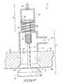
- A variety of possibilities exist for a valve body to include a portion of the chamber lid. As a first example, a portion of the chamber lid can include at least a part of a valve housing. In FIG. 2, a[0025]
valve 2 is shown having a combined valve body and a chamber lid identified as a group byreference numeral 4 and a valve actuator identified as a group by reference numeral6. As is apparent from FIG. 2, the part of ahousing 10 comprised by alid 8 between an outermost surface8aand aninnermost surface 8bis defined by acylindrical opening 20 havingside walls 12 inlid 8.Valve body 4 further includes astem 22 coincident with a central axis ofcylindrical opening 20 and positioned at least partially withincylindrical opening 20. - As a second example, a portion of the lid can include at least a part of a valve seat. In FIG. 2, the entirety of a[0026]
seat 14, as a plug-type seat, is betweeninnermost surface 8binside the chamber and outermost surface8aoutside the chamber. Further, the part ofseat 14 comprised bylid 8 is defined by a beveled lid surface aroundcylindrical opening 20 throughlid 8.Valve body 4 further includes aplug 16 complementary to the beveled lid surface ofseat 14. Accordingly, aplug seal 18 can be pressed againstseat 14 to closevalve body 4. - FIG. 2 shows one example of a pneumatic actuator. A[0027]
housing 24 encloses apiston 26. Aspring 28biases piston 26 upward and a connectingrod 30 linkingstem 22 topiston 26. A bellows32 isolates any process chemical delivered through aprocess chemical inlet 34 from passing into valve actuator6. By applying a pressure signal to asignal inlet 36,piston 26 compresses downward againstspring 28 to movestem 22 downward andseparate plug seal 18 fromseat 14, openingvalve body 4. Accordingly, if a pressure signal is lost,valve body 4 will automatically close. - Turning to FIG. 3, a[0028]
valve 42 is shown having a combined valve body and a chamber lid identified as a group byreference numeral 44. As is apparent from FIG. 3, the part of ahousing 50 comprised by alid 48 between anoutermost surface 48aand aninnermost surface 48bis defined by acylindrical opening 60 havingside walls 52 inlid 48.Valve body 44 further includes astem 62 coincident with a central axis ofcylindrical opening 60 and positioned at least partially withincylindrical opening 60. Further, the entirety of aseat 54, as a diaphragm-type seat, is betweeninnermost surface 48binside the chamber andoutermost surface 48aoutside the chamber. The part ofseat 54 comprised bylid 48 is defined by an annular platform around acylindrical opening 80 throughlid 48.Valve body 44 further includes aplug 56 and adiaphragm 58 betweenplug 56 andseat 54. - As a third example of a valve body including a portion of the chamber lid, a portion of the lid can include at least a part of a process chemical inlet in the valve body. In FIG. 3,[0029]
process chemical inlet 74 passes throughlid 48 toside walls 52 opening intocylindrical opening 60. Accordingly,chemical inlet 74 is in what can be considered part ofhousing 50 though part oflid 48 as well as in further removed portions oflid 48. - FIG. 3 also shows another example of a pneumatic actuator. A[0030]
housing 64 encloses apiston 66, aspring 68biasing piston 66, and a connectingrod 70 linkingstem 62 topiston 66. A bellows72 isolates any process chemical delivered throughchemical inlet 74 from passing intovalve actuator 46 in the event that diaphragm58 ruptures. By reducing a pressure signal to asignal inlet 76,spring 68 compresses downward againstpiston 66 to movestem 62 downward and compressdiaphragm 58 againstseat 54, closingvalve body 4. Accordingly, if a pressure signal is lost,valve body 4 will automatically close. - In a still further aspect of the invention, a CVD apparatus includes a deposition chamber having a lid and an opening defined by side walls extending between an inner surface of the lid inside the chamber and an outer surface of the lid outside the chamber. The apparatus can further include a valve body having a housing and a seat. At least a part of the housing can include at least a part of the outer surface of the lid, at least a part of the opening side walls of the lid, or both. At least a part of the seat can include at least a part of the inner surface of the lid, at least a part of the opening side walls of the lid, or both.[0031]
- According to an aspect of the invention, a deposition method includes providing a process chemical supply line to a chamber wall of a deposition chamber. The supply line can be temporarily isolated from the deposition chamber at the wall. While isolated at the wall, the supply line can be filled with chemical through a supply valve upstream from the wall. The supply line can be filled to a first pressure. Chemical can be released from the supply line into the deposition chamber at the wall. The supply line can again be temporarily isolated from the deposition chamber at the wall. In keeping with indications above, such a deposition method can be a CVD method, and may be particularly suited as an ALD method.[0032]
- Given the short cycle times in ALD where a process chemical is successively delivered to a deposition chamber, purged from the deposition chamber, and again delivered, an ability to pressurize chemical in advance for direct delivery at a chamber wall can be advantageous. For example, the supply line can be re-pressurized during purging. Accordingly, the method can include closing the supply valve after filling the supply line with chemical and before releasing chemical into the deposition chamber. Further, the method can include, while releasing chemical into the chamber, maintaining chemical in the supply line between the supply valve and the wall at about a second pressure. The first and second pressures can be about the same or can be different depending upon desired process conditions.[0033]
- In compliance with the statute, the invention has been described in language more or less specific as to structural and methodical features. It is to be understood, however, that the invention is not limited to the specific features shown and described, since the means herein disclosed comprise preferred forms of putting the invention into effect. The invention is, therefore, claimed in any of its forms or modifications within the proper scope of the appended claims appropriately interpreted in accordance with the doctrine of equivalents.[0034]
Claims (36)
1. A chemical vapor deposition apparatus comprising:
a deposition chamber defined partly by a chamber wall, the chamber wall having an innermost surface inside the chamber and an outermost surface outside the chamber; and
a valve body having a seat between the innermost and outermost surfaces of the chamber wall.
2. The apparatus ofclaim 1 wherein the chemical vapor deposition apparatus comprises an atomic layer deposition apparatus.
3. The apparatus ofclaim 1 wherein the chamber wall comprises a lid.
4. The apparatus ofclaim 1 wherein the valve body includes a portion of the chamber wall as at least a part of the seat.
5. The apparatus ofclaim 1 wherein the valve body comprises at least a part of a valve housing between the innermost and outermost surfaces of the chamber wall.
6. The apparatus ofclaim 5 wherein the valve body includes a portion of the chamber wall as at least a part of the valve housing.
7. The apparatus ofclaim 1 further comprising at least a part of a process chemical inlet to the valve body between the innermost and outermost surfaces of the chamber wall.
8. The apparatus ofclaim 7 wherein the chamber wall forms at least a part of the chemical inlet.
9. A chemical vapor deposition apparatus comprising:
a deposition chamber having a lid;
a process chemical opening completely through the lid; and
an isolation mechanism proximate the chemical opening, the lid being integral to the isolation mechanism and the isolation mechanism selectively isolating the deposition chamber from receiving material through the chemical opening.
10. The apparatus ofclaim 9 wherein the chemical vapor deposition apparatus comprises an atomic layer deposition apparatus.
11. The apparatus ofclaim 9 wherein the isolation mechanism comprises a valve.
12. The apparatus ofclaim 11 wherein the lid comprises at least a part of a seat of the valve.
13. The apparatus ofclaim 11 wherein the lid comprises at least a part of a housing of the valve.
14. The apparatus ofclaim 11 wherein the lid comprises at least a part of a process chemical inlet to the valve.
15. A chemical vapor deposition apparatus comprising:
a deposition chamber having a lid; and
a valve body including a portion of the lid as part of the valve body, the valve body selectively shutting off flow of a process chemical into the chamber, adjusting the flow rate of the chemical into the chamber, or both.
16. The apparatus ofclaim 15 wherein the chemical vapor deposition apparatus comprises an atomic layer deposition apparatus.
17. The apparatus ofclaim 15 wherein at a 50% open position as indicated by a stem position the valve body provides a flow rate of no more than about 50% of a maximum flow rate through the valve body.
18. The apparatus ofclaim 15 wherein the portion of the lid comprises at least a part of a valve housing.
19. The apparatus ofclaim 18 wherein the part of the valve housing comprised by the portion of the lid is defined by a cylindrical opening in the lid, the valve body further comprising a stem coincident with a central axis of the cylindrical opening and positioned at least partially within the cylindrical opening.
20. The apparatus ofclaim 15 wherein the portion of the lid comprises at least a part of a valve seat.
21. The apparatus ofclaim 20 wherein the entirety of the valve seat is between an innermost surface of the lid inside the chamber and an outermost surface of the lid outside the chamber.
22. The apparatus ofclaim 20 wherein the valve seat comprises a plug seat or a diaphragm seat.
23. The apparatus ofclaim 20 wherein the part of the valve seat comprised by the portion of the lid is defined by a beveled lid surface around a cylindrical opening through the lid, the valve body further comprising a plug complementary to the beveled lid surface.
24. The apparatus ofclaim 20 wherein the part of the valve seat comprised by the portion of the lid is defined by an annular platform around a cylindrical opening through the lid, the valve body further comprising a plug and a diaphragm between the plug and annular platform.
25. The apparatus ofclaim 15 wherein the portion of the lid comprises at least a part of a process chemical inlet in the valve body.
26. The apparatus ofclaim 25 wherein the apparatus further comprises a process chemical inlet through the lid to the chemical inlet in the valve body.
27. A chemical vapor deposition apparatus comprising:
a deposition chamber having a lid, the lid having an inner surface inside the chamber, an outer surface outside the chamber, and an opening defined by sidewalls extending between the inner and outer surfaces;
a valve body having a housing and a seat;
at least a part of the housing comprising at least a part of the outer surface of the lid, at least a part of the opening sidewalls of the lid, or both; and
at least a part of the seat comprising at least a part of the inner surface of the lid, at least a part of the opening sidewalls of the lid, or both.
28. The apparatus ofclaim 27 wherein the chemical vapor deposition apparatus comprises an atomic layer deposition apparatus.
29. The apparatus ofclaim 27 further comprising a process chemical inlet to the valve body, a lid portion between the inner surface and the outer surface forming at least a part of the chemical inlet.
30. A chemical vapor deposition method comprising:
providing a process chemical supply line to a chamber wall partly defining a deposition chamber;
temporarily isolating the supply line from the deposition chamber at the chamber wall;
while isolated at the chamber wall, filling the supply line with chemical through a supply valve upstream from the chamber wall, the supply line being filled to a first pressure;
releasing chemical from the supply line into the deposition chamber at the chamber wall; and
again temporarily isolating the supply line from the deposition chamber at the chamber wall.
31. The method ofclaim 30 wherein the chamber wall comprises a lid.
32. The method ofclaim 30 further comprising, while releasing chemical into the deposition chamber, maintaining chemical in the supply line between the supply valve and the chamber wall at about a second pressure.
33. The method ofclaim 31 wherein the first and second pressures are about the same.
34. The method ofclaim 30 further comprising closing the supply valve after the filling the supply line with chemical and before the releasing the chemical into the deposition chamber.
35. The method ofclaim 30 further comprising purging chemical from the deposition chamber after again temporarily isolating the supply line from the deposition chamber.
36. The method ofclaim 30 wherein the chemical vapor deposition method comprises atomic layer deposition.
Priority Applications (2)
| Application Number | Priority Date | Filing Date | Title |
|---|---|---|---|
| US09/810,387US20020129768A1 (en) | 2001-03-15 | 2001-03-15 | Chemical vapor deposition apparatuses and deposition methods |
| US11/175,523US20050241581A1 (en) | 2001-03-15 | 2005-07-05 | Chemical vapor deposition apparatuses and deposition methods |
Applications Claiming Priority (1)
| Application Number | Priority Date | Filing Date | Title |
|---|---|---|---|
| US09/810,387US20020129768A1 (en) | 2001-03-15 | 2001-03-15 | Chemical vapor deposition apparatuses and deposition methods |
Related Child Applications (1)
| Application Number | Title | Priority Date | Filing Date |
|---|---|---|---|
| US11/175,523DivisionUS20050241581A1 (en) | 2001-03-15 | 2005-07-05 | Chemical vapor deposition apparatuses and deposition methods |
Publications (1)
| Publication Number | Publication Date |
|---|---|
| US20020129768A1true US20020129768A1 (en) | 2002-09-19 |
Family
ID=25203736
Family Applications (2)
| Application Number | Title | Priority Date | Filing Date |
|---|---|---|---|
| US09/810,387AbandonedUS20020129768A1 (en) | 2001-03-15 | 2001-03-15 | Chemical vapor deposition apparatuses and deposition methods |
| US11/175,523AbandonedUS20050241581A1 (en) | 2001-03-15 | 2005-07-05 | Chemical vapor deposition apparatuses and deposition methods |
Family Applications After (1)
| Application Number | Title | Priority Date | Filing Date |
|---|---|---|---|
| US11/175,523AbandonedUS20050241581A1 (en) | 2001-03-15 | 2005-07-05 | Chemical vapor deposition apparatuses and deposition methods |
Country Status (1)
| Country | Link |
|---|---|
| US (2) | US20020129768A1 (en) |
Cited By (305)
| Publication number | Priority date | Publication date | Assignee | Title |
|---|---|---|---|---|
| US20030119328A1 (en)* | 2001-12-26 | 2003-06-26 | Tokyo Electron Limited | Plasma processing apparatus, and cleaning method therefor |
| US20030131792A1 (en)* | 2002-01-17 | 2003-07-17 | Jin-Jun Park | Pressure control apparatus and method of establshing a desired level of pressure within at least one processing chamber |
| US20030221616A1 (en)* | 2002-05-28 | 2003-12-04 | Micron Technology, Inc. | Magnetically-actuatable throttle valve |
| US20040094092A1 (en)* | 2002-02-25 | 2004-05-20 | Derderian Garo J. | Apparatus for improved delivery of metastable species |
| US20040144310A1 (en)* | 2001-08-17 | 2004-07-29 | Campbell Philip H. | CVD apparatuses and methods of forming a layer over a semiconductor substrate |
| US20050120954A1 (en)* | 2002-05-24 | 2005-06-09 | Carpenter Craig M. | Apparatus for controlling gas pulsing in processes for depositing materials onto micro-device workpieces |
| US20050133161A1 (en)* | 2002-07-08 | 2005-06-23 | Carpenter Craig M. | Apparatus and method for depositing materials onto microelectronic workpieces |
| US20050145337A1 (en)* | 2002-04-25 | 2005-07-07 | Derderian Garo J. | Apparatus for forming thin layers of materials on micro-device workpieces |
| US20050155551A1 (en)* | 2004-01-19 | 2005-07-21 | Byoung-Jae Bae | Deposition apparatus and related methods including a pulse fluid supplier having a buffer |
| US20050160983A1 (en)* | 2002-01-17 | 2005-07-28 | Sundew Technologies, Llc | ALD apparatus and method |
| US20050191416A1 (en)* | 2002-08-15 | 2005-09-01 | Cem Basceri | Methods of gas delivery for deposition processes and methods of depositing material on a substrate |
| US20050217585A1 (en)* | 2004-04-01 | 2005-10-06 | Blomiley Eric R | Substrate susceptor for receiving a substrate to be deposited upon |
| US20050217569A1 (en)* | 2004-04-01 | 2005-10-06 | Nirmal Ramaswamy | Methods of depositing an elemental silicon-comprising material over a semiconductor substrate and methods of cleaning an internal wall of a chamber |
| US20050223985A1 (en)* | 2004-04-08 | 2005-10-13 | Blomiley Eric R | Deposition apparatuses, methods of assessing the temperature of semiconductor wafer substrates within deposition apparatuses, and methods for deposition of epitaxial semiconductive material |
| US20050223993A1 (en)* | 2004-04-08 | 2005-10-13 | Blomiley Eric R | Deposition apparatuses; methods for assessing alignments of substrates within deposition apparatuses; and methods for assessing thicknesses of deposited layers within deposition apparatuses |
| US20050241581A1 (en)* | 2001-03-15 | 2005-11-03 | Carpenter Craig M | Chemical vapor deposition apparatuses and deposition methods |
| US20060021574A1 (en)* | 2004-08-02 | 2006-02-02 | Veeco Instruments Inc. | Multi-gas distribution injector for chemical vapor deposition reactors |
| US20060045970A1 (en)* | 2004-08-31 | 2006-03-02 | Jung-Hun Seo | ALD thin film deposition apparatus and thin film deposition method using same |
| US7056806B2 (en) | 2003-09-17 | 2006-06-06 | Micron Technology, Inc. | Microfeature workpiece processing apparatus and methods for controlling deposition of materials on microfeature workpieces |
| US20070020394A1 (en)* | 2002-06-26 | 2007-01-25 | Micron Technology, Inc. | Methods and apparatus for vapor processing of micro-device workpieces |
| US7235138B2 (en) | 2003-08-21 | 2007-06-26 | Micron Technology, Inc. | Microfeature workpiece processing apparatus and methods for batch deposition of materials on microfeature workpieces |
| US7258892B2 (en) | 2003-12-10 | 2007-08-21 | Micron Technology, Inc. | Methods and systems for controlling temperature during microfeature workpiece processing, e.g., CVD deposition |
| US7282239B2 (en) | 2003-09-18 | 2007-10-16 | Micron Technology, Inc. | Systems and methods for depositing material onto microfeature workpieces in reaction chambers |
| US7323231B2 (en) | 2003-10-09 | 2008-01-29 | Micron Technology, Inc. | Apparatus and methods for plasma vapor deposition processes |
| US7335396B2 (en) | 2003-04-24 | 2008-02-26 | Micron Technology, Inc. | Methods for controlling mass flow rates and pressures in passageways coupled to reaction chambers and systems for depositing material onto microfeature workpieces in reaction chambers |
| US7344755B2 (en) | 2003-08-21 | 2008-03-18 | Micron Technology, Inc. | Methods and apparatus for processing microfeature workpieces; methods for conditioning ALD reaction chambers |
| US7422635B2 (en) | 2003-08-28 | 2008-09-09 | Micron Technology, Inc. | Methods and apparatus for processing microfeature workpieces, e.g., for depositing materials on microfeature workpieces |
| US20090159424A1 (en)* | 2007-12-19 | 2009-06-25 | Wei Liu | Dual zone gas injection nozzle |
| US20090208649A1 (en)* | 2006-04-18 | 2009-08-20 | Christopher Mark Bailey | Vacuum Pumping System |
| US7581511B2 (en) | 2003-10-10 | 2009-09-01 | Micron Technology, Inc. | Apparatus and methods for manufacturing microfeatures on workpieces using plasma vapor processes |
| US7584942B2 (en) | 2004-03-31 | 2009-09-08 | Micron Technology, Inc. | Ampoules for producing a reaction gas and systems for depositing materials onto microfeature workpieces in reaction chambers |
| US7588804B2 (en) | 2002-08-15 | 2009-09-15 | Micron Technology, Inc. | Reactors with isolated gas connectors and methods for depositing materials onto micro-device workpieces |
| US7647886B2 (en) | 2003-10-15 | 2010-01-19 | Micron Technology, Inc. | Systems for depositing material onto workpieces in reaction chambers and methods for removing byproducts from reaction chambers |
| US7699932B2 (en) | 2004-06-02 | 2010-04-20 | Micron Technology, Inc. | Reactors, systems and methods for depositing thin films onto microfeature workpieces |
| US7906393B2 (en) | 2004-01-28 | 2011-03-15 | Micron Technology, Inc. | Methods for forming small-scale capacitor structures |
| US20110274837A1 (en)* | 2009-02-09 | 2011-11-10 | Beneq Oy | Ald reactor, method for loading ald reactor, and production line |
| US8133554B2 (en) | 2004-05-06 | 2012-03-13 | Micron Technology, Inc. | Methods for depositing material onto microfeature workpieces in reaction chambers and systems for depositing materials onto microfeature workpieces |
| US20120114856A1 (en)* | 2007-12-18 | 2012-05-10 | Asm Genitech Korea Ltd. | Deposition apparatus |
| US20130019802A1 (en)* | 2010-12-23 | 2013-01-24 | Centrotherm Sitec Gmbh | Nozzle arrangement and cvd-reactor |
| US9790596B1 (en)* | 2013-01-30 | 2017-10-17 | Kyocera Corporation | Gas nozzle and plasma device employing same |
| US10287684B2 (en)* | 2014-07-08 | 2019-05-14 | Kokusai Electric Corporation | Substrate processing apparatus |
| US10395900B2 (en)* | 2016-06-17 | 2019-08-27 | Samsung Electronics Co., Ltd. | Plasma processing apparatus |
| US11056344B2 (en) | 2017-08-30 | 2021-07-06 | Asm Ip Holding B.V. | Layer forming method |
| US11053590B2 (en)* | 2014-08-15 | 2021-07-06 | Applied Materials, Inc. | Nozzle for uniform plasma processing |
| US11069510B2 (en) | 2017-08-30 | 2021-07-20 | Asm Ip Holding B.V. | Substrate processing apparatus |
| US11087997B2 (en) | 2018-10-31 | 2021-08-10 | Asm Ip Holding B.V. | Substrate processing apparatus for processing substrates |
| US11094546B2 (en) | 2017-10-05 | 2021-08-17 | Asm Ip Holding B.V. | Method for selectively depositing a metallic film on a substrate |
| US11094582B2 (en) | 2016-07-08 | 2021-08-17 | Asm Ip Holding B.V. | Selective deposition method to form air gaps |
| US11101370B2 (en) | 2016-05-02 | 2021-08-24 | Asm Ip Holding B.V. | Method of forming a germanium oxynitride film |
| US11114294B2 (en) | 2019-03-08 | 2021-09-07 | Asm Ip Holding B.V. | Structure including SiOC layer and method of forming same |
| US11114283B2 (en) | 2018-03-16 | 2021-09-07 | Asm Ip Holding B.V. | Reactor, system including the reactor, and methods of manufacturing and using same |
| USD930782S1 (en) | 2019-08-22 | 2021-09-14 | Asm Ip Holding B.V. | Gas distributor |
| US11127617B2 (en) | 2017-11-27 | 2021-09-21 | Asm Ip Holding B.V. | Storage device for storing wafer cassettes for use with a batch furnace |
| US11127589B2 (en) | 2019-02-01 | 2021-09-21 | Asm Ip Holding B.V. | Method of topology-selective film formation of silicon oxide |
| USD931978S1 (en) | 2019-06-27 | 2021-09-28 | Asm Ip Holding B.V. | Showerhead vacuum transport |
| US11139308B2 (en) | 2015-12-29 | 2021-10-05 | Asm Ip Holding B.V. | Atomic layer deposition of III-V compounds to form V-NAND devices |
| US11158513B2 (en) | 2018-12-13 | 2021-10-26 | Asm Ip Holding B.V. | Methods for forming a rhenium-containing film on a substrate by a cyclical deposition process and related semiconductor device structures |
| US11164955B2 (en) | 2017-07-18 | 2021-11-02 | Asm Ip Holding B.V. | Methods for forming a semiconductor device structure and related semiconductor device structures |
| USD935572S1 (en) | 2019-05-24 | 2021-11-09 | Asm Ip Holding B.V. | Gas channel plate |
| US11171025B2 (en) | 2019-01-22 | 2021-11-09 | Asm Ip Holding B.V. | Substrate processing device |
| US11168395B2 (en) | 2018-06-29 | 2021-11-09 | Asm Ip Holding B.V. | Temperature-controlled flange and reactor system including same |
| US11205585B2 (en) | 2016-07-28 | 2021-12-21 | Asm Ip Holding B.V. | Substrate processing apparatus and method of operating the same |
| US11217444B2 (en) | 2018-11-30 | 2022-01-04 | Asm Ip Holding B.V. | Method for forming an ultraviolet radiation responsive metal oxide-containing film |
| US11222772B2 (en) | 2016-12-14 | 2022-01-11 | Asm Ip Holding B.V. | Substrate processing apparatus |
| USD940837S1 (en) | 2019-08-22 | 2022-01-11 | Asm Ip Holding B.V. | Electrode |
| US11227782B2 (en) | 2019-07-31 | 2022-01-18 | Asm Ip Holding B.V. | Vertical batch furnace assembly |
| US11227789B2 (en) | 2019-02-20 | 2022-01-18 | Asm Ip Holding B.V. | Method and apparatus for filling a recess formed within a substrate surface |
| US11230766B2 (en) | 2018-03-29 | 2022-01-25 | Asm Ip Holding B.V. | Substrate processing apparatus and method |
| US11232963B2 (en) | 2018-10-03 | 2022-01-25 | Asm Ip Holding B.V. | Substrate processing apparatus and method |
| US11233133B2 (en) | 2015-10-21 | 2022-01-25 | Asm Ip Holding B.V. | NbMC layers |
| US11242598B2 (en) | 2015-06-26 | 2022-02-08 | Asm Ip Holding B.V. | Structures including metal carbide material, devices including the structures, and methods of forming same |
| US11244825B2 (en) | 2018-11-16 | 2022-02-08 | Asm Ip Holding B.V. | Methods for depositing a transition metal chalcogenide film on a substrate by a cyclical deposition process |
| US11251068B2 (en) | 2018-10-19 | 2022-02-15 | Asm Ip Holding B.V. | Substrate processing apparatus and substrate processing method |
| US11251035B2 (en) | 2016-12-22 | 2022-02-15 | Asm Ip Holding B.V. | Method of forming a structure on a substrate |
| US11251040B2 (en) | 2019-02-20 | 2022-02-15 | Asm Ip Holding B.V. | Cyclical deposition method including treatment step and apparatus for same |
| USD944946S1 (en) | 2019-06-14 | 2022-03-01 | Asm Ip Holding B.V. | Shower plate |
| US11270899B2 (en) | 2018-06-04 | 2022-03-08 | Asm Ip Holding B.V. | Wafer handling chamber with moisture reduction |
| US11274369B2 (en) | 2018-09-11 | 2022-03-15 | Asm Ip Holding B.V. | Thin film deposition method |
| US11282698B2 (en) | 2019-07-19 | 2022-03-22 | Asm Ip Holding B.V. | Method of forming topology-controlled amorphous carbon polymer film |
| US11289326B2 (en) | 2019-05-07 | 2022-03-29 | Asm Ip Holding B.V. | Method for reforming amorphous carbon polymer film |
| US11286562B2 (en) | 2018-06-08 | 2022-03-29 | Asm Ip Holding B.V. | Gas-phase chemical reactor and method of using same |
| US11286558B2 (en) | 2019-08-23 | 2022-03-29 | Asm Ip Holding B.V. | Methods for depositing a molybdenum nitride film on a surface of a substrate by a cyclical deposition process and related semiconductor device structures including a molybdenum nitride film |
| US11296189B2 (en) | 2018-06-21 | 2022-04-05 | Asm Ip Holding B.V. | Method for depositing a phosphorus doped silicon arsenide film and related semiconductor device structures |
| US11295980B2 (en) | 2017-08-30 | 2022-04-05 | Asm Ip Holding B.V. | Methods for depositing a molybdenum metal film over a dielectric surface of a substrate by a cyclical deposition process and related semiconductor device structures |
| USD947913S1 (en) | 2019-05-17 | 2022-04-05 | Asm Ip Holding B.V. | Susceptor shaft |
| US11306395B2 (en) | 2017-06-28 | 2022-04-19 | Asm Ip Holding B.V. | Methods for depositing a transition metal nitride film on a substrate by atomic layer deposition and related deposition apparatus |
| USD949319S1 (en) | 2019-08-22 | 2022-04-19 | Asm Ip Holding B.V. | Exhaust duct |
| US11315794B2 (en) | 2019-10-21 | 2022-04-26 | Asm Ip Holding B.V. | Apparatus and methods for selectively etching films |
| US11342216B2 (en) | 2019-02-20 | 2022-05-24 | Asm Ip Holding B.V. | Cyclical deposition method and apparatus for filling a recess formed within a substrate surface |
| US11342164B2 (en)* | 2011-12-16 | 2022-05-24 | Taiwan Semiconductor Manufacturing Company, Ltd. | High density plasma chemical vapor deposition chamber and method of using |
| US11339476B2 (en) | 2019-10-08 | 2022-05-24 | Asm Ip Holding B.V. | Substrate processing device having connection plates, substrate processing method |
| US11345999B2 (en) | 2019-06-06 | 2022-05-31 | Asm Ip Holding B.V. | Method of using a gas-phase reactor system including analyzing exhausted gas |
| US11355338B2 (en) | 2019-05-10 | 2022-06-07 | Asm Ip Holding B.V. | Method of depositing material onto a surface and structure formed according to the method |
| US11361990B2 (en) | 2018-05-28 | 2022-06-14 | Asm Ip Holding B.V. | Substrate processing method and device manufactured by using the same |
| US11374112B2 (en) | 2017-07-19 | 2022-06-28 | Asm Ip Holding B.V. | Method for depositing a group IV semiconductor and related semiconductor device structures |
| US11378337B2 (en) | 2019-03-28 | 2022-07-05 | Asm Ip Holding B.V. | Door opener and substrate processing apparatus provided therewith |
| US11387106B2 (en) | 2018-02-14 | 2022-07-12 | Asm Ip Holding B.V. | Method for depositing a ruthenium-containing film on a substrate by a cyclical deposition process |
| US11387120B2 (en) | 2017-09-28 | 2022-07-12 | Asm Ip Holding B.V. | Chemical dispensing apparatus and methods for dispensing a chemical to a reaction chamber |
| US11393690B2 (en) | 2018-01-19 | 2022-07-19 | Asm Ip Holding B.V. | Deposition method |
| US11390950B2 (en) | 2017-01-10 | 2022-07-19 | Asm Ip Holding B.V. | Reactor system and method to reduce residue buildup during a film deposition process |
| US11390946B2 (en) | 2019-01-17 | 2022-07-19 | Asm Ip Holding B.V. | Methods of forming a transition metal containing film on a substrate by a cyclical deposition process |
| US11390945B2 (en) | 2019-07-03 | 2022-07-19 | Asm Ip Holding B.V. | Temperature control assembly for substrate processing apparatus and method of using same |
| US20220228263A1 (en)* | 2019-06-07 | 2022-07-21 | Lam Research Corporation | Independently adjustable flowpath conductance in multi-station semiconductor processing |
| US11398382B2 (en) | 2018-03-27 | 2022-07-26 | Asm Ip Holding B.V. | Method of forming an electrode on a substrate and a semiconductor device structure including an electrode |
| US11396702B2 (en) | 2016-11-15 | 2022-07-26 | Asm Ip Holding B.V. | Gas supply unit and substrate processing apparatus including the gas supply unit |
| US11401605B2 (en) | 2019-11-26 | 2022-08-02 | Asm Ip Holding B.V. | Substrate processing apparatus |
| US11411088B2 (en) | 2018-11-16 | 2022-08-09 | Asm Ip Holding B.V. | Methods for forming a metal silicate film on a substrate in a reaction chamber and related semiconductor device structures |
| US11410851B2 (en) | 2017-02-15 | 2022-08-09 | Asm Ip Holding B.V. | Methods for forming a metallic film on a substrate by cyclical deposition and related semiconductor device structures |
| US11417545B2 (en) | 2017-08-08 | 2022-08-16 | Asm Ip Holding B.V. | Radiation shield |
| US11414760B2 (en) | 2018-10-08 | 2022-08-16 | Asm Ip Holding B.V. | Substrate support unit, thin film deposition apparatus including the same, and substrate processing apparatus including the same |
| US11424119B2 (en) | 2019-03-08 | 2022-08-23 | Asm Ip Holding B.V. | Method for selective deposition of silicon nitride layer and structure including selectively-deposited silicon nitride layer |
| US11430640B2 (en) | 2019-07-30 | 2022-08-30 | Asm Ip Holding B.V. | Substrate processing apparatus |
| US11430674B2 (en) | 2018-08-22 | 2022-08-30 | Asm Ip Holding B.V. | Sensor array, apparatus for dispensing a vapor phase reactant to a reaction chamber and related methods |
| US11437241B2 (en) | 2020-04-08 | 2022-09-06 | Asm Ip Holding B.V. | Apparatus and methods for selectively etching silicon oxide films |
| US11443926B2 (en) | 2019-07-30 | 2022-09-13 | Asm Ip Holding B.V. | Substrate processing apparatus |
| US11447861B2 (en)* | 2016-12-15 | 2022-09-20 | Asm Ip Holding B.V. | Sequential infiltration synthesis apparatus and a method of forming a patterned structure |
| US11447864B2 (en) | 2019-04-19 | 2022-09-20 | Asm Ip Holding B.V. | Layer forming method and apparatus |
| US11450529B2 (en) | 2019-11-26 | 2022-09-20 | Asm Ip Holding B.V. | Methods for selectively forming a target film on a substrate comprising a first dielectric surface and a second metallic surface |
| USD965044S1 (en) | 2019-08-19 | 2022-09-27 | Asm Ip Holding B.V. | Susceptor shaft |
| USD965524S1 (en) | 2019-08-19 | 2022-10-04 | Asm Ip Holding B.V. | Susceptor support |
| US11469098B2 (en) | 2018-05-08 | 2022-10-11 | Asm Ip Holding B.V. | Methods for depositing an oxide film on a substrate by a cyclical deposition process and related device structures |
| US11476109B2 (en) | 2019-06-11 | 2022-10-18 | Asm Ip Holding B.V. | Method of forming an electronic structure using reforming gas, system for performing the method, and structure formed using the method |
| US11473195B2 (en) | 2018-03-01 | 2022-10-18 | Asm Ip Holding B.V. | Semiconductor processing apparatus and a method for processing a substrate |
| US11482418B2 (en) | 2018-02-20 | 2022-10-25 | Asm Ip Holding B.V. | Substrate processing method and apparatus |
| US11482533B2 (en) | 2019-02-20 | 2022-10-25 | Asm Ip Holding B.V. | Apparatus and methods for plug fill deposition in 3-D NAND applications |
| US11482412B2 (en) | 2018-01-19 | 2022-10-25 | Asm Ip Holding B.V. | Method for depositing a gap-fill layer by plasma-assisted deposition |
| US11488854B2 (en) | 2020-03-11 | 2022-11-01 | Asm Ip Holding B.V. | Substrate handling device with adjustable joints |
| US11488819B2 (en) | 2018-12-04 | 2022-11-01 | Asm Ip Holding B.V. | Method of cleaning substrate processing apparatus |
| US11495459B2 (en) | 2019-09-04 | 2022-11-08 | Asm Ip Holding B.V. | Methods for selective deposition using a sacrificial capping layer |
| US11492703B2 (en) | 2018-06-27 | 2022-11-08 | Asm Ip Holding B.V. | Cyclic deposition methods for forming metal-containing material and films and structures including the metal-containing material |
| US11501973B2 (en) | 2018-01-16 | 2022-11-15 | Asm Ip Holding B.V. | Method for depositing a material film on a substrate within a reaction chamber by a cyclical deposition process and related device structures |
| US11499226B2 (en) | 2018-11-02 | 2022-11-15 | Asm Ip Holding B.V. | Substrate supporting unit and a substrate processing device including the same |
| US11499222B2 (en) | 2018-06-27 | 2022-11-15 | Asm Ip Holding B.V. | Cyclic deposition methods for forming metal-containing material and films and structures including the metal-containing material |
| US11501956B2 (en) | 2012-10-12 | 2022-11-15 | Asm Ip Holding B.V. | Semiconductor reaction chamber showerhead |
| US11501968B2 (en) | 2019-11-15 | 2022-11-15 | Asm Ip Holding B.V. | Method for providing a semiconductor device with silicon filled gaps |
| US11515187B2 (en) | 2020-05-01 | 2022-11-29 | Asm Ip Holding B.V. | Fast FOUP swapping with a FOUP handler |
| US11515188B2 (en) | 2019-05-16 | 2022-11-29 | Asm Ip Holding B.V. | Wafer boat handling device, vertical batch furnace and method |
| US11521851B2 (en) | 2020-02-03 | 2022-12-06 | Asm Ip Holding B.V. | Method of forming structures including a vanadium or indium layer |
| US11527400B2 (en) | 2019-08-23 | 2022-12-13 | Asm Ip Holding B.V. | Method for depositing silicon oxide film having improved quality by peald using bis(diethylamino)silane |
| US11527403B2 (en) | 2019-12-19 | 2022-12-13 | Asm Ip Holding B.V. | Methods for filling a gap feature on a substrate surface and related semiconductor structures |
| US11530876B2 (en) | 2020-04-24 | 2022-12-20 | Asm Ip Holding B.V. | Vertical batch furnace assembly comprising a cooling gas supply |
| US11532757B2 (en) | 2016-10-27 | 2022-12-20 | Asm Ip Holding B.V. | Deposition of charge trapping layers |
| US11530483B2 (en) | 2018-06-21 | 2022-12-20 | Asm Ip Holding B.V. | Substrate processing system |
| US11551925B2 (en) | 2019-04-01 | 2023-01-10 | Asm Ip Holding B.V. | Method for manufacturing a semiconductor device |
| US11551912B2 (en) | 2020-01-20 | 2023-01-10 | Asm Ip Holding B.V. | Method of forming thin film and method of modifying surface of thin film |
| US11557474B2 (en) | 2019-07-29 | 2023-01-17 | Asm Ip Holding B.V. | Methods for selective deposition utilizing n-type dopants and/or alternative dopants to achieve high dopant incorporation |
| USD975665S1 (en) | 2019-05-17 | 2023-01-17 | Asm Ip Holding B.V. | Susceptor shaft |
| US11562901B2 (en) | 2019-09-25 | 2023-01-24 | Asm Ip Holding B.V. | Substrate processing method |
| US11572620B2 (en) | 2018-11-06 | 2023-02-07 | Asm Ip Holding B.V. | Methods for selectively depositing an amorphous silicon film on a substrate |
| US11581186B2 (en) | 2016-12-15 | 2023-02-14 | Asm Ip Holding B.V. | Sequential infiltration synthesis apparatus |
| US11587814B2 (en) | 2019-07-31 | 2023-02-21 | Asm Ip Holding B.V. | Vertical batch furnace assembly |
| US11587821B2 (en) | 2017-08-08 | 2023-02-21 | Asm Ip Holding B.V. | Substrate lift mechanism and reactor including same |
| US11587815B2 (en) | 2019-07-31 | 2023-02-21 | Asm Ip Holding B.V. | Vertical batch furnace assembly |
| US11594450B2 (en) | 2019-08-22 | 2023-02-28 | Asm Ip Holding B.V. | Method for forming a structure with a hole |
| USD979506S1 (en) | 2019-08-22 | 2023-02-28 | Asm Ip Holding B.V. | Insulator |
| US11594600B2 (en) | 2019-11-05 | 2023-02-28 | Asm Ip Holding B.V. | Structures with doped semiconductor layers and methods and systems for forming same |
| USD980813S1 (en) | 2021-05-11 | 2023-03-14 | Asm Ip Holding B.V. | Gas flow control plate for substrate processing apparatus |
| US11605528B2 (en) | 2019-07-09 | 2023-03-14 | Asm Ip Holding B.V. | Plasma device using coaxial waveguide, and substrate treatment method |
| USD980814S1 (en) | 2021-05-11 | 2023-03-14 | Asm Ip Holding B.V. | Gas distributor for substrate processing apparatus |
| US11610774B2 (en) | 2019-10-02 | 2023-03-21 | Asm Ip Holding B.V. | Methods for forming a topographically selective silicon oxide film by a cyclical plasma-enhanced deposition process |
| US11610775B2 (en) | 2016-07-28 | 2023-03-21 | Asm Ip Holding B.V. | Method and apparatus for filling a gap |
| USD981973S1 (en) | 2021-05-11 | 2023-03-28 | Asm Ip Holding B.V. | Reactor wall for substrate processing apparatus |
| US11615970B2 (en) | 2019-07-17 | 2023-03-28 | Asm Ip Holding B.V. | Radical assist ignition plasma system and method |
| US11626308B2 (en) | 2020-05-13 | 2023-04-11 | Asm Ip Holding B.V. | Laser alignment fixture for a reactor system |
| US11626316B2 (en) | 2019-11-20 | 2023-04-11 | Asm Ip Holding B.V. | Method of depositing carbon-containing material on a surface of a substrate, structure formed using the method, and system for forming the structure |
| US11629407B2 (en) | 2019-02-22 | 2023-04-18 | Asm Ip Holding B.V. | Substrate processing apparatus and method for processing substrates |
| US11629406B2 (en) | 2018-03-09 | 2023-04-18 | Asm Ip Holding B.V. | Semiconductor processing apparatus comprising one or more pyrometers for measuring a temperature of a substrate during transfer of the substrate |
| US11637011B2 (en) | 2019-10-16 | 2023-04-25 | Asm Ip Holding B.V. | Method of topology-selective film formation of silicon oxide |
| US11637014B2 (en) | 2019-10-17 | 2023-04-25 | Asm Ip Holding B.V. | Methods for selective deposition of doped semiconductor material |
| US11639548B2 (en) | 2019-08-21 | 2023-05-02 | Asm Ip Holding B.V. | Film-forming material mixed-gas forming device and film forming device |
| US11639811B2 (en) | 2017-11-27 | 2023-05-02 | Asm Ip Holding B.V. | Apparatus including a clean mini environment |
| US11643724B2 (en) | 2019-07-18 | 2023-05-09 | Asm Ip Holding B.V. | Method of forming structures using a neutral beam |
| US11646197B2 (en) | 2018-07-03 | 2023-05-09 | Asm Ip Holding B.V. | Method for depositing silicon-free carbon-containing film as gap-fill layer by pulse plasma-assisted deposition |
| US11646205B2 (en) | 2019-10-29 | 2023-05-09 | Asm Ip Holding B.V. | Methods of selectively forming n-type doped material on a surface, systems for selectively forming n-type doped material, and structures formed using same |
| US11644758B2 (en) | 2020-07-17 | 2023-05-09 | Asm Ip Holding B.V. | Structures and methods for use in photolithography |
| US11646184B2 (en) | 2019-11-29 | 2023-05-09 | Asm Ip Holding B.V. | Substrate processing apparatus |
| US11646204B2 (en) | 2020-06-24 | 2023-05-09 | Asm Ip Holding B.V. | Method for forming a layer provided with silicon |
| US11649546B2 (en) | 2016-07-08 | 2023-05-16 | Asm Ip Holding B.V. | Organic reactants for atomic layer deposition |
| US11658035B2 (en) | 2020-06-30 | 2023-05-23 | Asm Ip Holding B.V. | Substrate processing method |
| US11658029B2 (en) | 2018-12-14 | 2023-05-23 | Asm Ip Holding B.V. | Method of forming a device structure using selective deposition of gallium nitride and system for same |
| US11664267B2 (en) | 2019-07-10 | 2023-05-30 | Asm Ip Holding B.V. | Substrate support assembly and substrate processing device including the same |
| US11664199B2 (en) | 2018-10-19 | 2023-05-30 | Asm Ip Holding B.V. | Substrate processing apparatus and substrate processing method |
| US11664245B2 (en) | 2019-07-16 | 2023-05-30 | Asm Ip Holding B.V. | Substrate processing device |
| US11674220B2 (en) | 2020-07-20 | 2023-06-13 | Asm Ip Holding B.V. | Method for depositing molybdenum layers using an underlayer |
| US11676812B2 (en) | 2016-02-19 | 2023-06-13 | Asm Ip Holding B.V. | Method for forming silicon nitride film selectively on top/bottom portions |
| US11680839B2 (en) | 2019-08-05 | 2023-06-20 | Asm Ip Holding B.V. | Liquid level sensor for a chemical source vessel |
| US11688603B2 (en) | 2019-07-17 | 2023-06-27 | Asm Ip Holding B.V. | Methods of forming silicon germanium structures |
| US11685991B2 (en) | 2018-02-14 | 2023-06-27 | Asm Ip Holding B.V. | Method for depositing a ruthenium-containing film on a substrate by a cyclical deposition process |
| USD990441S1 (en) | 2021-09-07 | 2023-06-27 | Asm Ip Holding B.V. | Gas flow control plate |
| USD990534S1 (en) | 2020-09-11 | 2023-06-27 | Asm Ip Holding B.V. | Weighted lift pin |
| US11694892B2 (en) | 2016-07-28 | 2023-07-04 | Asm Ip Holding B.V. | Method and apparatus for filling a gap |
| US11705333B2 (en) | 2020-05-21 | 2023-07-18 | Asm Ip Holding B.V. | Structures including multiple carbon layers and methods of forming and using same |
| US11718913B2 (en) | 2018-06-04 | 2023-08-08 | Asm Ip Holding B.V. | Gas distribution system and reactor system including same |
| US11725277B2 (en) | 2011-07-20 | 2023-08-15 | Asm Ip Holding B.V. | Pressure transmitter for a semiconductor processing environment |
| US11725280B2 (en) | 2020-08-26 | 2023-08-15 | Asm Ip Holding B.V. | Method for forming metal silicon oxide and metal silicon oxynitride layers |
| US11735422B2 (en) | 2019-10-10 | 2023-08-22 | Asm Ip Holding B.V. | Method of forming a photoresist underlayer and structure including same |
| US11735414B2 (en) | 2018-02-06 | 2023-08-22 | Asm Ip Holding B.V. | Method of post-deposition treatment for silicon oxide film |
| US11742198B2 (en) | 2019-03-08 | 2023-08-29 | Asm Ip Holding B.V. | Structure including SiOCN layer and method of forming same |
| US11742189B2 (en) | 2015-03-12 | 2023-08-29 | Asm Ip Holding B.V. | Multi-zone reactor, system including the reactor, and method of using the same |
| US11767589B2 (en) | 2020-05-29 | 2023-09-26 | Asm Ip Holding B.V. | Substrate processing device |
| US11769682B2 (en) | 2017-08-09 | 2023-09-26 | Asm Ip Holding B.V. | Storage apparatus for storing cassettes for substrates and processing apparatus equipped therewith |
| US11776846B2 (en) | 2020-02-07 | 2023-10-03 | Asm Ip Holding B.V. | Methods for depositing gap filling fluids and related systems and devices |
| US11781243B2 (en) | 2020-02-17 | 2023-10-10 | Asm Ip Holding B.V. | Method for depositing low temperature phosphorous-doped silicon |
| US11781221B2 (en) | 2019-05-07 | 2023-10-10 | Asm Ip Holding B.V. | Chemical source vessel with dip tube |
| US11795545B2 (en) | 2014-10-07 | 2023-10-24 | Asm Ip Holding B.V. | Multiple temperature range susceptor, assembly, reactor and system including the susceptor, and methods of using the same |
| US11804364B2 (en) | 2020-05-19 | 2023-10-31 | Asm Ip Holding B.V. | Substrate processing apparatus |
| US11804388B2 (en) | 2018-09-11 | 2023-10-31 | Asm Ip Holding B.V. | Substrate processing apparatus and method |
| US11802338B2 (en) | 2017-07-26 | 2023-10-31 | Asm Ip Holding B.V. | Chemical treatment, deposition and/or infiltration apparatus and method for using the same |
| US11810788B2 (en) | 2016-11-01 | 2023-11-07 | Asm Ip Holding B.V. | Methods for forming a transition metal niobium nitride film on a substrate by atomic layer deposition and related semiconductor device structures |
| US11814747B2 (en) | 2019-04-24 | 2023-11-14 | Asm Ip Holding B.V. | Gas-phase reactor system-with a reaction chamber, a solid precursor source vessel, a gas distribution system, and a flange assembly |
| US11823866B2 (en) | 2020-04-02 | 2023-11-21 | Asm Ip Holding B.V. | Thin film forming method |
| US11823876B2 (en) | 2019-09-05 | 2023-11-21 | Asm Ip Holding B.V. | Substrate processing apparatus |
| US11821078B2 (en) | 2020-04-15 | 2023-11-21 | Asm Ip Holding B.V. | Method for forming precoat film and method for forming silicon-containing film |
| US11830730B2 (en) | 2017-08-29 | 2023-11-28 | Asm Ip Holding B.V. | Layer forming method and apparatus |
| US11830738B2 (en) | 2020-04-03 | 2023-11-28 | Asm Ip Holding B.V. | Method for forming barrier layer and method for manufacturing semiconductor device |
| US11828707B2 (en) | 2020-02-04 | 2023-11-28 | Asm Ip Holding B.V. | Method and apparatus for transmittance measurements of large articles |
| US11827981B2 (en) | 2020-10-14 | 2023-11-28 | Asm Ip Holding B.V. | Method of depositing material on stepped structure |
| US11840761B2 (en) | 2019-12-04 | 2023-12-12 | Asm Ip Holding B.V. | Substrate processing apparatus |
| US11848200B2 (en) | 2017-05-08 | 2023-12-19 | Asm Ip Holding B.V. | Methods for selectively forming a silicon nitride film on a substrate and related semiconductor device structures |
| US11876356B2 (en) | 2020-03-11 | 2024-01-16 | Asm Ip Holding B.V. | Lockout tagout assembly and system and method of using same |
| US11873557B2 (en) | 2020-10-22 | 2024-01-16 | Asm Ip Holding B.V. | Method of depositing vanadium metal |
| US11885023B2 (en) | 2018-10-01 | 2024-01-30 | Asm Ip Holding B.V. | Substrate retaining apparatus, system including the apparatus, and method of using same |
| US11887857B2 (en) | 2020-04-24 | 2024-01-30 | Asm Ip Holding B.V. | Methods and systems for depositing a layer comprising vanadium, nitrogen, and a further element |
| US11885013B2 (en) | 2019-12-17 | 2024-01-30 | Asm Ip Holding B.V. | Method of forming vanadium nitride layer and structure including the vanadium nitride layer |
| US11885020B2 (en) | 2020-12-22 | 2024-01-30 | Asm Ip Holding B.V. | Transition metal deposition method |
| USD1012873S1 (en) | 2020-09-24 | 2024-01-30 | Asm Ip Holding B.V. | Electrode for semiconductor processing apparatus |
| US11891696B2 (en) | 2020-11-30 | 2024-02-06 | Asm Ip Holding B.V. | Injector configured for arrangement within a reaction chamber of a substrate processing apparatus |
| US11898243B2 (en) | 2020-04-24 | 2024-02-13 | Asm Ip Holding B.V. | Method of forming vanadium nitride-containing layer |
| US11901179B2 (en) | 2020-10-28 | 2024-02-13 | Asm Ip Holding B.V. | Method and device for depositing silicon onto substrates |
| US11923181B2 (en) | 2019-11-29 | 2024-03-05 | Asm Ip Holding B.V. | Substrate processing apparatus for minimizing the effect of a filling gas during substrate processing |
| US11923190B2 (en) | 2018-07-03 | 2024-03-05 | Asm Ip Holding B.V. | Method for depositing silicon-free carbon-containing film as gap-fill layer by pulse plasma-assisted deposition |
| US11929251B2 (en) | 2019-12-02 | 2024-03-12 | Asm Ip Holding B.V. | Substrate processing apparatus having electrostatic chuck and substrate processing method |
| US11939673B2 (en) | 2018-02-23 | 2024-03-26 | Asm Ip Holding B.V. | Apparatus for detecting or monitoring for a chemical precursor in a high temperature environment |
| US11946137B2 (en) | 2020-12-16 | 2024-04-02 | Asm Ip Holding B.V. | Runout and wobble measurement fixtures |
| US11959168B2 (en) | 2020-04-29 | 2024-04-16 | Asm Ip Holding B.V. | Solid source precursor vessel |
| US11961741B2 (en) | 2020-03-12 | 2024-04-16 | Asm Ip Holding B.V. | Method for fabricating layer structure having target topological profile |
| US11967488B2 (en) | 2013-02-01 | 2024-04-23 | Asm Ip Holding B.V. | Method for treatment of deposition reactor |
| USD1023959S1 (en) | 2021-05-11 | 2024-04-23 | Asm Ip Holding B.V. | Electrode for substrate processing apparatus |
| US11976359B2 (en) | 2020-01-06 | 2024-05-07 | Asm Ip Holding B.V. | Gas supply assembly, components thereof, and reactor system including same |
| US11976352B2 (en)* | 2018-02-12 | 2024-05-07 | Merck Patent Gmbh | Methods of vapor deposition of ruthenium using an oxygen-free co-reactant |
| US11987881B2 (en) | 2020-05-22 | 2024-05-21 | Asm Ip Holding B.V. | Apparatus for depositing thin films using hydrogen peroxide |
| US11986868B2 (en) | 2020-02-28 | 2024-05-21 | Asm Ip Holding B.V. | System dedicated for parts cleaning |
| US11996292B2 (en) | 2019-10-25 | 2024-05-28 | Asm Ip Holding B.V. | Methods for filling a gap feature on a substrate surface and related semiconductor structures |
| US11993847B2 (en) | 2020-01-08 | 2024-05-28 | Asm Ip Holding B.V. | Injector |
| US11996289B2 (en) | 2020-04-16 | 2024-05-28 | Asm Ip Holding B.V. | Methods of forming structures including silicon germanium and silicon layers, devices formed using the methods, and systems for performing the methods |
| US11996309B2 (en) | 2019-05-16 | 2024-05-28 | Asm Ip Holding B.V. | Wafer boat handling device, vertical batch furnace and method |
| US12006572B2 (en) | 2019-10-08 | 2024-06-11 | Asm Ip Holding B.V. | Reactor system including a gas distribution assembly for use with activated species and method of using same |
| US12009241B2 (en) | 2019-10-14 | 2024-06-11 | Asm Ip Holding B.V. | Vertical batch furnace assembly with detector to detect cassette |
| US12009224B2 (en) | 2020-09-29 | 2024-06-11 | Asm Ip Holding B.V. | Apparatus and method for etching metal nitrides |
| US12020934B2 (en) | 2020-07-08 | 2024-06-25 | Asm Ip Holding B.V. | Substrate processing method |
| US12025484B2 (en) | 2018-05-08 | 2024-07-02 | Asm Ip Holding B.V. | Thin film forming method |
| US12027365B2 (en) | 2020-11-24 | 2024-07-02 | Asm Ip Holding B.V. | Methods for filling a gap and related systems and devices |
| US12033885B2 (en) | 2020-01-06 | 2024-07-09 | Asm Ip Holding B.V. | Channeled lift pin |
| US12040199B2 (en) | 2018-11-28 | 2024-07-16 | Asm Ip Holding B.V. | Substrate processing apparatus for processing substrates |
| US12040184B2 (en) | 2017-10-30 | 2024-07-16 | Asm Ip Holding B.V. | Methods for forming a semiconductor structure and related semiconductor structures |
| US12040177B2 (en) | 2020-08-18 | 2024-07-16 | Asm Ip Holding B.V. | Methods for forming a laminate film by cyclical plasma-enhanced deposition processes |
| US12040200B2 (en) | 2017-06-20 | 2024-07-16 | Asm Ip Holding B.V. | Semiconductor processing apparatus and methods for calibrating a semiconductor processing apparatus |
| US12051602B2 (en) | 2020-05-04 | 2024-07-30 | Asm Ip Holding B.V. | Substrate processing system for processing substrates with an electronics module located behind a door in a front wall of the substrate processing system |
| US12051567B2 (en) | 2020-10-07 | 2024-07-30 | Asm Ip Holding B.V. | Gas supply unit and substrate processing apparatus including gas supply unit |
| US12057314B2 (en) | 2020-05-15 | 2024-08-06 | Asm Ip Holding B.V. | Methods for silicon germanium uniformity control using multiple precursors |
| US12074022B2 (en) | 2020-08-27 | 2024-08-27 | Asm Ip Holding B.V. | Method and system for forming patterned structures using multiple patterning process |
| US12087586B2 (en) | 2020-04-15 | 2024-09-10 | Asm Ip Holding B.V. | Method of forming chromium nitride layer and structure including the chromium nitride layer |
| US12106944B2 (en) | 2020-06-02 | 2024-10-01 | Asm Ip Holding B.V. | Rotating substrate support |
| US12107005B2 (en) | 2020-10-06 | 2024-10-01 | Asm Ip Holding B.V. | Deposition method and an apparatus for depositing a silicon-containing material |
| US12112940B2 (en) | 2019-07-19 | 2024-10-08 | Asm Ip Holding B.V. | Method of forming topology-controlled amorphous carbon polymer film |
| US12125700B2 (en) | 2020-01-16 | 2024-10-22 | Asm Ip Holding B.V. | Method of forming high aspect ratio features |
| US12129545B2 (en) | 2020-12-22 | 2024-10-29 | Asm Ip Holding B.V. | Precursor capsule, a vessel and a method |
| US12131885B2 (en) | 2020-12-22 | 2024-10-29 | Asm Ip Holding B.V. | Plasma treatment device having matching box |
| US12148609B2 (en) | 2020-09-16 | 2024-11-19 | Asm Ip Holding B.V. | Silicon oxide deposition method |
| US12154824B2 (en) | 2020-08-14 | 2024-11-26 | Asm Ip Holding B.V. | Substrate processing method |
| US12159788B2 (en) | 2020-12-14 | 2024-12-03 | Asm Ip Holding B.V. | Method of forming structures for threshold voltage control |
| US12169361B2 (en) | 2019-07-30 | 2024-12-17 | Asm Ip Holding B.V. | Substrate processing apparatus and method |
| US12173402B2 (en) | 2018-02-15 | 2024-12-24 | Asm Ip Holding B.V. | Method of forming a transition metal containing film on a substrate by a cyclical deposition process, a method for supplying a transition metal halide compound to a reaction chamber, and related vapor deposition apparatus |
| US12173404B2 (en) | 2020-03-17 | 2024-12-24 | Asm Ip Holding B.V. | Method of depositing epitaxial material, structure formed using the method, and system for performing the method |
| US12195852B2 (en) | 2020-11-23 | 2025-01-14 | Asm Ip Holding B.V. | Substrate processing apparatus with an injector |
| US12209308B2 (en) | 2020-11-12 | 2025-01-28 | Asm Ip Holding B.V. | Reactor and related methods |
| US12211742B2 (en) | 2020-09-10 | 2025-01-28 | Asm Ip Holding B.V. | Methods for depositing gap filling fluid |
| US12218269B2 (en) | 2020-02-13 | 2025-02-04 | Asm Ip Holding B.V. | Substrate processing apparatus including light receiving device and calibration method of light receiving device |
| USD1060598S1 (en) | 2021-12-03 | 2025-02-04 | Asm Ip Holding B.V. | Split showerhead cover |
| US12217946B2 (en) | 2020-10-15 | 2025-02-04 | Asm Ip Holding B.V. | Method of manufacturing semiconductor device, and substrate treatment apparatus using ether-CAT |
| US12217954B2 (en) | 2020-08-25 | 2025-02-04 | Asm Ip Holding B.V. | Method of cleaning a surface |
| US12218000B2 (en) | 2020-09-25 | 2025-02-04 | Asm Ip Holding B.V. | Semiconductor processing method |
| US12221357B2 (en) | 2020-04-24 | 2025-02-11 | Asm Ip Holding B.V. | Methods and apparatus for stabilizing vanadium compounds |
| US12230531B2 (en) | 2018-04-09 | 2025-02-18 | Asm Ip Holding B.V. | Substrate supporting apparatus, substrate processing apparatus including the same, and substrate processing method |
| US12243742B2 (en) | 2020-04-21 | 2025-03-04 | Asm Ip Holding B.V. | Method for processing a substrate |
| US12240760B2 (en) | 2016-03-18 | 2025-03-04 | Asm Ip Holding B.V. | Aligned carbon nanotubes |
| US12243757B2 (en) | 2020-05-21 | 2025-03-04 | Asm Ip Holding B.V. | Flange and apparatus for processing substrates |
| US12241158B2 (en) | 2020-07-20 | 2025-03-04 | Asm Ip Holding B.V. | Method for forming structures including transition metal layers |
| US12243747B2 (en) | 2020-04-24 | 2025-03-04 | Asm Ip Holding B.V. | Methods of forming structures including vanadium boride and vanadium phosphide layers |
| US12247286B2 (en) | 2019-08-09 | 2025-03-11 | Asm Ip Holding B.V. | Heater assembly including cooling apparatus and method of using same |
| US12252785B2 (en) | 2019-06-10 | 2025-03-18 | Asm Ip Holding B.V. | Method for cleaning quartz epitaxial chambers |
| US12255053B2 (en) | 2020-12-10 | 2025-03-18 | Asm Ip Holding B.V. | Methods and systems for depositing a layer |
| US12266524B2 (en) | 2020-06-16 | 2025-04-01 | Asm Ip Holding B.V. | Method for depositing boron containing silicon germanium layers |
| US12272527B2 (en) | 2018-05-09 | 2025-04-08 | Asm Ip Holding B.V. | Apparatus for use with hydrogen radicals and method of using same |
| US12276023B2 (en) | 2017-08-04 | 2025-04-15 | Asm Ip Holding B.V. | Showerhead assembly for distributing a gas within a reaction chamber |
| US12278129B2 (en) | 2020-03-04 | 2025-04-15 | Asm Ip Holding B.V. | Alignment fixture for a reactor system |
| US12288710B2 (en) | 2020-12-18 | 2025-04-29 | Asm Ip Holding B.V. | Wafer processing apparatus with a rotatable table |
| US12322591B2 (en) | 2020-07-27 | 2025-06-03 | Asm Ip Holding B.V. | Thin film deposition process |
| US12378665B2 (en) | 2018-10-26 | 2025-08-05 | Asm Ip Holding B.V. | High temperature coatings for a preclean and etch apparatus and related methods |
| US12406846B2 (en) | 2020-05-26 | 2025-09-02 | Asm Ip Holding B.V. | Method for depositing boron and gallium containing silicon germanium layers |
| US12410515B2 (en) | 2020-01-29 | 2025-09-09 | Asm Ip Holding B.V. | Contaminant trap system for a reactor system |
| US12431354B2 (en) | 2020-07-01 | 2025-09-30 | Asm Ip Holding B.V. | Silicon nitride and silicon oxide deposition methods using fluorine inhibitor |
| US12428726B2 (en) | 2019-10-08 | 2025-09-30 | Asm Ip Holding B.V. | Gas injection system and reactor system including same |
| US12431334B2 (en) | 2020-02-13 | 2025-09-30 | Asm Ip Holding B.V. | Gas distribution assembly |
| US12444599B2 (en) | 2021-12-08 | 2025-10-14 | Asm Ip Holding B.V. | Method for forming an ultraviolet radiation responsive metal oxide-containing film |
Citations (33)
| Publication number | Priority date | Publication date | Assignee | Title |
|---|---|---|---|---|
| US4170690A (en)* | 1977-03-18 | 1979-10-09 | Rohm And Haas Company | Process of coating weatherable, abrasion resistant coating and coated articles |
| US4319737A (en)* | 1978-04-26 | 1982-03-16 | Waterfield Engineering Limited | Diaphram valve |
| US4517375A (en)* | 1980-10-02 | 1985-05-14 | Dynamit Nobel Ag | Stable aqueous impregnating solutions prepared from hydrolyzed alkyltrialkoxysilanes |
| US4592933A (en)* | 1984-06-29 | 1986-06-03 | International Business Machines Corporation | High efficiency homogeneous chemical vapor deposition |
| US4724159A (en)* | 1985-10-14 | 1988-02-09 | Semiconductor Energy Laboratory Co., Ltd. | Conductive layer deposition method with a microwave enhanced CVD system |
| US4747367A (en)* | 1986-06-12 | 1988-05-31 | Crystal Specialties, Inc. | Method and apparatus for producing a constant flow, constant pressure chemical vapor deposition |
| US4761269A (en)* | 1986-06-12 | 1988-08-02 | Crystal Specialties, Inc. | Apparatus for depositing material on a substrate |
| US4798809A (en)* | 1985-12-11 | 1989-01-17 | Canon Kabushiki Kaisha | Process for preparing photoelectromotive force member |
| US4872947A (en)* | 1986-12-19 | 1989-10-10 | Applied Materials, Inc. | CVD of silicon oxide using TEOS decomposition and in-situ planarization process |
| US4949669A (en)* | 1988-12-20 | 1990-08-21 | Texas Instruments Incorporated | Gas flow systems in CCVD reactors |
| US4965090A (en)* | 1988-01-13 | 1990-10-23 | U.S. Philips Corporation | Method for the plasma-activated reactive deposition of electrically conductive multicomponent material from a gas phase |
| US4971832A (en)* | 1988-03-02 | 1990-11-20 | Canon Kabushiki Kaisha | HR-CVD process for the formation of a functional deposited film on a substrate with application of a voltage in the range of -5 to -100 V |
| US5000113A (en)* | 1986-12-19 | 1991-03-19 | Applied Materials, Inc. | Thermal CVD/PECVD reactor and use for thermal chemical vapor deposition of silicon dioxide and in-situ multi-step planarized process |
| US5002928A (en)* | 1987-06-04 | 1991-03-26 | Toa Nenryo Kogyo Kabushiki Kaisha | Method for forming oxide superconducting films with an ultrasonic wave sprayer |
| US5068871A (en)* | 1989-08-04 | 1991-11-26 | Kabushiki Kaisha Toyota Chuo Kenkyusho | Process for synthesizing diamond and apparatus therefor |
| US5522934A (en)* | 1994-04-26 | 1996-06-04 | Tokyo Electron Limited | Plasma processing apparatus using vertical gas inlets one on top of another |
| US5620523A (en)* | 1994-04-11 | 1997-04-15 | Canon Sales Co., Inc. | Apparatus for forming film |
| US5772771A (en)* | 1995-12-13 | 1998-06-30 | Applied Materials, Inc. | Deposition chamber for improved deposition thickness uniformity |
| US5792272A (en)* | 1995-07-10 | 1998-08-11 | Watkins-Johnson Company | Plasma enhanced chemical processing reactor and method |
| US5853484A (en)* | 1995-10-28 | 1998-12-29 | Lg Semicon Co., Ltd. | Gas distribution system and method for chemical vapor deposition apparatus |
| US5885358A (en)* | 1996-07-09 | 1999-03-23 | Applied Materials, Inc. | Gas injection slit nozzle for a plasma process reactor |
| US5925411A (en)* | 1990-07-16 | 1999-07-20 | Siliconix Incorporated | Gas-based substrate deposition protection |
| US5993916A (en)* | 1996-07-12 | 1999-11-30 | Applied Materials, Inc. | Method for substrate processing with improved throughput and yield |
| US6110531A (en)* | 1991-02-25 | 2000-08-29 | Symetrix Corporation | Method and apparatus for preparing integrated circuit thin films by chemical vapor deposition |
| US6132552A (en)* | 1998-02-19 | 2000-10-17 | Micron Technology, Inc. | Method and apparatus for controlling the temperature of a gas distribution plate in a process reactor |
| US6228563B1 (en)* | 1999-09-17 | 2001-05-08 | Gasonics International Corporation | Method and apparatus for removing post-etch residues and other adherent matrices |
| US6294026B1 (en)* | 1996-11-26 | 2001-09-25 | Siemens Aktiengesellschaft | Distribution plate for a reaction chamber with multiple gas inlets and separate mass flow control loops |
| US6331212B1 (en)* | 2000-04-17 | 2001-12-18 | Avansys, Llc | Methods and apparatus for thermally processing wafers |
| US6453992B1 (en)* | 1999-05-10 | 2002-09-24 | Hyundai Electronics Industries Co., Ltd. | Temperature controllable gas distributor |
| US20020155632A1 (en)* | 2001-02-21 | 2002-10-24 | Shunpei Yamazaki | Method and apparatus for film deposition |
| US20030033980A1 (en)* | 2001-08-17 | 2003-02-20 | Campbell Philip H. | CVD apparatuses and methods of forming a layer over a semiconductor substrate |
| US20030045098A1 (en)* | 2001-08-31 | 2003-03-06 | Applied Materials, Inc. | Method and apparatus for processing a wafer |
| US6812157B1 (en)* | 1999-06-24 | 2004-11-02 | Prasad Narhar Gadgil | Apparatus for atomic layer chemical vapor deposition |
Family Cites Families (9)
| Publication number | Priority date | Publication date | Assignee | Title |
|---|---|---|---|---|
| US3110319A (en)* | 1962-01-15 | 1963-11-12 | Shinko Seiki Kabushiki Kaisha | High vacuum valve |
| DE2750928A1 (en)* | 1977-11-15 | 1979-05-17 | Maschf Augsburg Nuernberg Ag | FUEL INJECTION NOZZLE FOR COMBUSTION MACHINES |
| DE3637452A1 (en)* | 1986-11-04 | 1988-05-19 | Pagendarm Beschichtungstechnik | FLOW CONTROL DEVICE |
| US6056994A (en)* | 1988-12-27 | 2000-05-02 | Symetrix Corporation | Liquid deposition methods of fabricating layered superlattice materials |
| BR9204887A (en)* | 1991-12-23 | 1993-06-29 | Comision Nac Energ Atom | PROCESS FOR FORMING A SOLID SUBSTRATE ON A PROPERTY FILM SIMILAR TO THE DIAMOND, THE SOLID BODIES SO COATED AND THE COVERED FILM SO OBTAINED |
| KR100190310B1 (en)* | 1992-09-03 | 1999-06-01 | 모리시따 요오이찌 | Two stage primary dry pump |
| JP2713167B2 (en)* | 1994-06-14 | 1998-02-16 | 日本電気株式会社 | Comparator |
| US5743457A (en)* | 1996-04-01 | 1998-04-28 | Ford Motor Company | Controlled zone solder dispensing |
| US20020129768A1 (en)* | 2001-03-15 | 2002-09-19 | Carpenter Craig M. | Chemical vapor deposition apparatuses and deposition methods |
- 2001
- 2001-03-15USUS09/810,387patent/US20020129768A1/ennot_activeAbandoned
- 2005
- 2005-07-05USUS11/175,523patent/US20050241581A1/ennot_activeAbandoned
Patent Citations (36)
| Publication number | Priority date | Publication date | Assignee | Title |
|---|---|---|---|---|
| US4170690A (en)* | 1977-03-18 | 1979-10-09 | Rohm And Haas Company | Process of coating weatherable, abrasion resistant coating and coated articles |
| US4319737A (en)* | 1978-04-26 | 1982-03-16 | Waterfield Engineering Limited | Diaphram valve |
| US4517375A (en)* | 1980-10-02 | 1985-05-14 | Dynamit Nobel Ag | Stable aqueous impregnating solutions prepared from hydrolyzed alkyltrialkoxysilanes |
| US4592933A (en)* | 1984-06-29 | 1986-06-03 | International Business Machines Corporation | High efficiency homogeneous chemical vapor deposition |
| US4724159A (en)* | 1985-10-14 | 1988-02-09 | Semiconductor Energy Laboratory Co., Ltd. | Conductive layer deposition method with a microwave enhanced CVD system |
| US4798809A (en)* | 1985-12-11 | 1989-01-17 | Canon Kabushiki Kaisha | Process for preparing photoelectromotive force member |
| US4747367A (en)* | 1986-06-12 | 1988-05-31 | Crystal Specialties, Inc. | Method and apparatus for producing a constant flow, constant pressure chemical vapor deposition |
| US4761269A (en)* | 1986-06-12 | 1988-08-02 | Crystal Specialties, Inc. | Apparatus for depositing material on a substrate |
| US5362526A (en)* | 1986-12-19 | 1994-11-08 | Applied Materials, Inc. | Plasma-enhanced CVD process using TEOS for depositing silicon oxide |
| US4872947A (en)* | 1986-12-19 | 1989-10-10 | Applied Materials, Inc. | CVD of silicon oxide using TEOS decomposition and in-situ planarization process |
| US5000113A (en)* | 1986-12-19 | 1991-03-19 | Applied Materials, Inc. | Thermal CVD/PECVD reactor and use for thermal chemical vapor deposition of silicon dioxide and in-situ multi-step planarized process |
| US5002928A (en)* | 1987-06-04 | 1991-03-26 | Toa Nenryo Kogyo Kabushiki Kaisha | Method for forming oxide superconducting films with an ultrasonic wave sprayer |
| US4965090A (en)* | 1988-01-13 | 1990-10-23 | U.S. Philips Corporation | Method for the plasma-activated reactive deposition of electrically conductive multicomponent material from a gas phase |
| US4971832A (en)* | 1988-03-02 | 1990-11-20 | Canon Kabushiki Kaisha | HR-CVD process for the formation of a functional deposited film on a substrate with application of a voltage in the range of -5 to -100 V |
| US4949669A (en)* | 1988-12-20 | 1990-08-21 | Texas Instruments Incorporated | Gas flow systems in CCVD reactors |
| US5068871A (en)* | 1989-08-04 | 1991-11-26 | Kabushiki Kaisha Toyota Chuo Kenkyusho | Process for synthesizing diamond and apparatus therefor |
| US5925411A (en)* | 1990-07-16 | 1999-07-20 | Siliconix Incorporated | Gas-based substrate deposition protection |
| US6110531A (en)* | 1991-02-25 | 2000-08-29 | Symetrix Corporation | Method and apparatus for preparing integrated circuit thin films by chemical vapor deposition |
| US5620523A (en)* | 1994-04-11 | 1997-04-15 | Canon Sales Co., Inc. | Apparatus for forming film |
| US5522934A (en)* | 1994-04-26 | 1996-06-04 | Tokyo Electron Limited | Plasma processing apparatus using vertical gas inlets one on top of another |
| US5792272A (en)* | 1995-07-10 | 1998-08-11 | Watkins-Johnson Company | Plasma enhanced chemical processing reactor and method |
| US5853484A (en)* | 1995-10-28 | 1998-12-29 | Lg Semicon Co., Ltd. | Gas distribution system and method for chemical vapor deposition apparatus |
| US5772771A (en)* | 1995-12-13 | 1998-06-30 | Applied Materials, Inc. | Deposition chamber for improved deposition thickness uniformity |
| US5885358A (en)* | 1996-07-09 | 1999-03-23 | Applied Materials, Inc. | Gas injection slit nozzle for a plasma process reactor |
| US5993916A (en)* | 1996-07-12 | 1999-11-30 | Applied Materials, Inc. | Method for substrate processing with improved throughput and yield |
| US6294026B1 (en)* | 1996-11-26 | 2001-09-25 | Siemens Aktiengesellschaft | Distribution plate for a reaction chamber with multiple gas inlets and separate mass flow control loops |
| US6132552A (en)* | 1998-02-19 | 2000-10-17 | Micron Technology, Inc. | Method and apparatus for controlling the temperature of a gas distribution plate in a process reactor |
| US6453992B1 (en)* | 1999-05-10 | 2002-09-24 | Hyundai Electronics Industries Co., Ltd. | Temperature controllable gas distributor |
| US6812157B1 (en)* | 1999-06-24 | 2004-11-02 | Prasad Narhar Gadgil | Apparatus for atomic layer chemical vapor deposition |
| US6333268B1 (en)* | 1999-09-17 | 2001-12-25 | Novellus Systems, Inc. | Method and apparatus for removing post-etch residues and other adherent matrices |
| US6228563B1 (en)* | 1999-09-17 | 2001-05-08 | Gasonics International Corporation | Method and apparatus for removing post-etch residues and other adherent matrices |
| US6331212B1 (en)* | 2000-04-17 | 2001-12-18 | Avansys, Llc | Methods and apparatus for thermally processing wafers |
| US20020155632A1 (en)* | 2001-02-21 | 2002-10-24 | Shunpei Yamazaki | Method and apparatus for film deposition |
| US20030033980A1 (en)* | 2001-08-17 | 2003-02-20 | Campbell Philip H. | CVD apparatuses and methods of forming a layer over a semiconductor substrate |
| US20040144310A1 (en)* | 2001-08-17 | 2004-07-29 | Campbell Philip H. | CVD apparatuses and methods of forming a layer over a semiconductor substrate |
| US20030045098A1 (en)* | 2001-08-31 | 2003-03-06 | Applied Materials, Inc. | Method and apparatus for processing a wafer |
Cited By (388)
| Publication number | Priority date | Publication date | Assignee | Title |
|---|---|---|---|---|
| US20050241581A1 (en)* | 2001-03-15 | 2005-11-03 | Carpenter Craig M | Chemical vapor deposition apparatuses and deposition methods |
| US20040144310A1 (en)* | 2001-08-17 | 2004-07-29 | Campbell Philip H. | CVD apparatuses and methods of forming a layer over a semiconductor substrate |
| US6849133B2 (en) | 2001-08-17 | 2005-02-01 | Micron Technology, Inc. | CVD apparatuses and methods of forming a layer over a semiconductor substrate |
| US20050112890A1 (en)* | 2001-08-17 | 2005-05-26 | Campbell Philip H. | CVD apparatuses and methods of forming a layer over a semiconductor substrate |
| US20030119328A1 (en)* | 2001-12-26 | 2003-06-26 | Tokyo Electron Limited | Plasma processing apparatus, and cleaning method therefor |
| US20100043888A1 (en)* | 2002-01-17 | 2010-02-25 | Sundew Technologies, Llc | Ald apparatus and method |
| US20030131792A1 (en)* | 2002-01-17 | 2003-07-17 | Jin-Jun Park | Pressure control apparatus and method of establshing a desired level of pressure within at least one processing chamber |
| US7052576B2 (en)* | 2002-01-17 | 2006-05-30 | Samsung Electronics Co., Ltd. | Pressure control apparatus and method of establishing a desired level of pressure within at least one processing chamber |
| US8012261B2 (en) | 2002-01-17 | 2011-09-06 | Sundew Technologies, Llc | ALD apparatus and method |
| US7635502B2 (en)* | 2002-01-17 | 2009-12-22 | Sundew Technologies, Llc | ALD apparatus and method |
| US20050160983A1 (en)* | 2002-01-17 | 2005-07-28 | Sundew Technologies, Llc | ALD apparatus and method |
| US7527693B2 (en) | 2002-02-25 | 2009-05-05 | Micron Technology, Inc. | Apparatus for improved delivery of metastable species |
| US7393562B2 (en) | 2002-02-25 | 2008-07-01 | Micron Technology, Inc. | Deposition methods for improved delivery of metastable species |
| US20040213908A1 (en)* | 2002-02-25 | 2004-10-28 | Derderian Garo J. | Deposition methods and apparatus for improved delivery of metastable species |
| US20040094092A1 (en)* | 2002-02-25 | 2004-05-20 | Derderian Garo J. | Apparatus for improved delivery of metastable species |
| US20050145337A1 (en)* | 2002-04-25 | 2005-07-07 | Derderian Garo J. | Apparatus for forming thin layers of materials on micro-device workpieces |
| US20050120954A1 (en)* | 2002-05-24 | 2005-06-09 | Carpenter Craig M. | Apparatus for controlling gas pulsing in processes for depositing materials onto micro-device workpieces |
| US7481887B2 (en) | 2002-05-24 | 2009-01-27 | Micron Technology, Inc. | Apparatus for controlling gas pulsing in processes for depositing materials onto micro-device workpieces |
| US20040237895A1 (en)* | 2002-05-28 | 2004-12-02 | Micron Technology, Inc. | Magnetically-actuatable throttle valve |
| US20030221616A1 (en)* | 2002-05-28 | 2003-12-04 | Micron Technology, Inc. | Magnetically-actuatable throttle valve |
| US20070020394A1 (en)* | 2002-06-26 | 2007-01-25 | Micron Technology, Inc. | Methods and apparatus for vapor processing of micro-device workpieces |
| US20050133161A1 (en)* | 2002-07-08 | 2005-06-23 | Carpenter Craig M. | Apparatus and method for depositing materials onto microelectronic workpieces |
| US7387685B2 (en) | 2002-07-08 | 2008-06-17 | Micron Technology, Inc. | Apparatus and method for depositing materials onto microelectronic workpieces |
| US7399499B2 (en) | 2002-08-15 | 2008-07-15 | Micron Technology, Inc. | Methods of gas delivery for deposition processes and methods of depositing material on a substrate |
| US20050191416A1 (en)* | 2002-08-15 | 2005-09-01 | Cem Basceri | Methods of gas delivery for deposition processes and methods of depositing material on a substrate |
| US7588804B2 (en) | 2002-08-15 | 2009-09-15 | Micron Technology, Inc. | Reactors with isolated gas connectors and methods for depositing materials onto micro-device workpieces |
| US7335396B2 (en) | 2003-04-24 | 2008-02-26 | Micron Technology, Inc. | Methods for controlling mass flow rates and pressures in passageways coupled to reaction chambers and systems for depositing material onto microfeature workpieces in reaction chambers |
| US7344755B2 (en) | 2003-08-21 | 2008-03-18 | Micron Technology, Inc. | Methods and apparatus for processing microfeature workpieces; methods for conditioning ALD reaction chambers |
| US7235138B2 (en) | 2003-08-21 | 2007-06-26 | Micron Technology, Inc. | Microfeature workpiece processing apparatus and methods for batch deposition of materials on microfeature workpieces |
| US7422635B2 (en) | 2003-08-28 | 2008-09-09 | Micron Technology, Inc. | Methods and apparatus for processing microfeature workpieces, e.g., for depositing materials on microfeature workpieces |
| US7279398B2 (en) | 2003-09-17 | 2007-10-09 | Micron Technology, Inc. | Microfeature workpiece processing apparatus and methods for controlling deposition of materials on microfeature workpieces |
| US7056806B2 (en) | 2003-09-17 | 2006-06-06 | Micron Technology, Inc. | Microfeature workpiece processing apparatus and methods for controlling deposition of materials on microfeature workpieces |
| US7282239B2 (en) | 2003-09-18 | 2007-10-16 | Micron Technology, Inc. | Systems and methods for depositing material onto microfeature workpieces in reaction chambers |
| US7323231B2 (en) | 2003-10-09 | 2008-01-29 | Micron Technology, Inc. | Apparatus and methods for plasma vapor deposition processes |
| US7581511B2 (en) | 2003-10-10 | 2009-09-01 | Micron Technology, Inc. | Apparatus and methods for manufacturing microfeatures on workpieces using plasma vapor processes |
| US7647886B2 (en) | 2003-10-15 | 2010-01-19 | Micron Technology, Inc. | Systems for depositing material onto workpieces in reaction chambers and methods for removing byproducts from reaction chambers |
| US7258892B2 (en) | 2003-12-10 | 2007-08-21 | Micron Technology, Inc. | Methods and systems for controlling temperature during microfeature workpiece processing, e.g., CVD deposition |
| US7771537B2 (en) | 2003-12-10 | 2010-08-10 | Micron Technology, Inc. | Methods and systems for controlling temperature during microfeature workpiece processing, E.G. CVD deposition |
| US8518184B2 (en) | 2003-12-10 | 2013-08-27 | Micron Technology, Inc. | Methods and systems for controlling temperature during microfeature workpiece processing, E.G., CVD deposition |
| US20050155551A1 (en)* | 2004-01-19 | 2005-07-21 | Byoung-Jae Bae | Deposition apparatus and related methods including a pulse fluid supplier having a buffer |
| US7906393B2 (en) | 2004-01-28 | 2011-03-15 | Micron Technology, Inc. | Methods for forming small-scale capacitor structures |
| US8384192B2 (en) | 2004-01-28 | 2013-02-26 | Micron Technology, Inc. | Methods for forming small-scale capacitor structures |
| US7584942B2 (en) | 2004-03-31 | 2009-09-08 | Micron Technology, Inc. | Ampoules for producing a reaction gas and systems for depositing materials onto microfeature workpieces in reaction chambers |
| US20050217569A1 (en)* | 2004-04-01 | 2005-10-06 | Nirmal Ramaswamy | Methods of depositing an elemental silicon-comprising material over a semiconductor substrate and methods of cleaning an internal wall of a chamber |
| US20050217585A1 (en)* | 2004-04-01 | 2005-10-06 | Blomiley Eric R | Substrate susceptor for receiving a substrate to be deposited upon |
| US20060180084A1 (en)* | 2004-04-01 | 2006-08-17 | Blomiley Eric R | Substrate susceptor for receiving a substrate to be deposited upon |
| US20060191483A1 (en)* | 2004-04-01 | 2006-08-31 | Blomiley Eric R | Substrate susceptor for receiving a substrate to be deposited upon |
| US20060254506A1 (en)* | 2004-04-01 | 2006-11-16 | Nirmal Ramaswamy | Methods of depositing an elemental silicon-comprising material over a substrate |
| US20060180087A1 (en)* | 2004-04-01 | 2006-08-17 | Blomiley Eric R | Substrate susceptor for receiving a substrate to be deposited upon |
| US20070012241A1 (en)* | 2004-04-08 | 2007-01-18 | Blomiley Eric R | Methods of assessing the temperature of semiconductor wafer substrates within deposition apparatuses |
| US20060231016A1 (en)* | 2004-04-08 | 2006-10-19 | Blomiley Eric R | Deposition apparatuses |
| US7662649B2 (en) | 2004-04-08 | 2010-02-16 | Micron Technology, Inc. | Methods for assessing alignments of substrates within deposition apparatuses; and methods for assessing thicknesses of deposited layers within deposition apparatuses |
| US20060216840A1 (en)* | 2004-04-08 | 2006-09-28 | Blomiley Eric R | Methods for assessing alignments of substrates within deposition apparatuses; and methods for assessing thicknesses of deposited layers within deposition apparatuses |
| US20050223993A1 (en)* | 2004-04-08 | 2005-10-13 | Blomiley Eric R | Deposition apparatuses; methods for assessing alignments of substrates within deposition apparatuses; and methods for assessing thicknesses of deposited layers within deposition apparatuses |
| US20050223985A1 (en)* | 2004-04-08 | 2005-10-13 | Blomiley Eric R | Deposition apparatuses, methods of assessing the temperature of semiconductor wafer substrates within deposition apparatuses, and methods for deposition of epitaxial semiconductive material |
| US9023436B2 (en) | 2004-05-06 | 2015-05-05 | Micron Technology, Inc. | Methods for depositing material onto microfeature workpieces in reaction chambers and systems for depositing materials onto microfeature workpieces |
| US8133554B2 (en) | 2004-05-06 | 2012-03-13 | Micron Technology, Inc. | Methods for depositing material onto microfeature workpieces in reaction chambers and systems for depositing materials onto microfeature workpieces |
| US7699932B2 (en) | 2004-06-02 | 2010-04-20 | Micron Technology, Inc. | Reactors, systems and methods for depositing thin films onto microfeature workpieces |
| US20060021574A1 (en)* | 2004-08-02 | 2006-02-02 | Veeco Instruments Inc. | Multi-gas distribution injector for chemical vapor deposition reactors |
| US20100300359A1 (en)* | 2004-08-02 | 2010-12-02 | Veeco Instruments Inc. | Multi-gas distribution injector for chemical vapor deposition reactors |
| US20060045970A1 (en)* | 2004-08-31 | 2006-03-02 | Jung-Hun Seo | ALD thin film deposition apparatus and thin film deposition method using same |
| US20090208649A1 (en)* | 2006-04-18 | 2009-08-20 | Christopher Mark Bailey | Vacuum Pumping System |
| US9133836B2 (en)* | 2006-04-18 | 2015-09-15 | Edwards Limited | Vacuum pumping system |
| US20120114856A1 (en)* | 2007-12-18 | 2012-05-10 | Asm Genitech Korea Ltd. | Deposition apparatus |
| US8747948B2 (en)* | 2007-12-18 | 2014-06-10 | Asm Genitech Korea Ltd. | Deposition apparatus |
| US20090159424A1 (en)* | 2007-12-19 | 2009-06-25 | Wei Liu | Dual zone gas injection nozzle |
| US8137463B2 (en)* | 2007-12-19 | 2012-03-20 | Applied Materials, Inc. | Dual zone gas injection nozzle |
| US20110274837A1 (en)* | 2009-02-09 | 2011-11-10 | Beneq Oy | Ald reactor, method for loading ald reactor, and production line |
| US20130019802A1 (en)* | 2010-12-23 | 2013-01-24 | Centrotherm Sitec Gmbh | Nozzle arrangement and cvd-reactor |
| US11725277B2 (en) | 2011-07-20 | 2023-08-15 | Asm Ip Holding B.V. | Pressure transmitter for a semiconductor processing environment |
| US11342164B2 (en)* | 2011-12-16 | 2022-05-24 | Taiwan Semiconductor Manufacturing Company, Ltd. | High density plasma chemical vapor deposition chamber and method of using |
| US12020905B2 (en) | 2011-12-16 | 2024-06-25 | Taiwan Semiconductor Manufacturing Company, Ltd. | Method of using high density plasma chemical vapor deposition chamber |
| US11501956B2 (en) | 2012-10-12 | 2022-11-15 | Asm Ip Holding B.V. | Semiconductor reaction chamber showerhead |
| US9790596B1 (en)* | 2013-01-30 | 2017-10-17 | Kyocera Corporation | Gas nozzle and plasma device employing same |
| US11967488B2 (en) | 2013-02-01 | 2024-04-23 | Asm Ip Holding B.V. | Method for treatment of deposition reactor |
| US10287684B2 (en)* | 2014-07-08 | 2019-05-14 | Kokusai Electric Corporation | Substrate processing apparatus |
| US11053590B2 (en)* | 2014-08-15 | 2021-07-06 | Applied Materials, Inc. | Nozzle for uniform plasma processing |
| US11795545B2 (en) | 2014-10-07 | 2023-10-24 | Asm Ip Holding B.V. | Multiple temperature range susceptor, assembly, reactor and system including the susceptor, and methods of using the same |
| US11742189B2 (en) | 2015-03-12 | 2023-08-29 | Asm Ip Holding B.V. | Multi-zone reactor, system including the reactor, and method of using the same |
| US11242598B2 (en) | 2015-06-26 | 2022-02-08 | Asm Ip Holding B.V. | Structures including metal carbide material, devices including the structures, and methods of forming same |
| US11233133B2 (en) | 2015-10-21 | 2022-01-25 | Asm Ip Holding B.V. | NbMC layers |
| US11956977B2 (en) | 2015-12-29 | 2024-04-09 | Asm Ip Holding B.V. | Atomic layer deposition of III-V compounds to form V-NAND devices |
| US11139308B2 (en) | 2015-12-29 | 2021-10-05 | Asm Ip Holding B.V. | Atomic layer deposition of III-V compounds to form V-NAND devices |
| US11676812B2 (en) | 2016-02-19 | 2023-06-13 | Asm Ip Holding B.V. | Method for forming silicon nitride film selectively on top/bottom portions |
| US12240760B2 (en) | 2016-03-18 | 2025-03-04 | Asm Ip Holding B.V. | Aligned carbon nanotubes |
| US11101370B2 (en) | 2016-05-02 | 2021-08-24 | Asm Ip Holding B.V. | Method of forming a germanium oxynitride film |
| US10903053B2 (en)* | 2016-06-17 | 2021-01-26 | Samsung Electronics Co., Ltd. | Plasma processing apparatus |
| US10395900B2 (en)* | 2016-06-17 | 2019-08-27 | Samsung Electronics Co., Ltd. | Plasma processing apparatus |
| US11749562B2 (en) | 2016-07-08 | 2023-09-05 | Asm Ip Holding B.V. | Selective deposition method to form air gaps |
| US11094582B2 (en) | 2016-07-08 | 2021-08-17 | Asm Ip Holding B.V. | Selective deposition method to form air gaps |
| US11649546B2 (en) | 2016-07-08 | 2023-05-16 | Asm Ip Holding B.V. | Organic reactants for atomic layer deposition |
| US11694892B2 (en) | 2016-07-28 | 2023-07-04 | Asm Ip Holding B.V. | Method and apparatus for filling a gap |
| US11205585B2 (en) | 2016-07-28 | 2021-12-21 | Asm Ip Holding B.V. | Substrate processing apparatus and method of operating the same |
| US11610775B2 (en) | 2016-07-28 | 2023-03-21 | Asm Ip Holding B.V. | Method and apparatus for filling a gap |
| US11532757B2 (en) | 2016-10-27 | 2022-12-20 | Asm Ip Holding B.V. | Deposition of charge trapping layers |
| US11810788B2 (en) | 2016-11-01 | 2023-11-07 | Asm Ip Holding B.V. | Methods for forming a transition metal niobium nitride film on a substrate by atomic layer deposition and related semiconductor device structures |
| US11396702B2 (en) | 2016-11-15 | 2022-07-26 | Asm Ip Holding B.V. | Gas supply unit and substrate processing apparatus including the gas supply unit |
| US11222772B2 (en) | 2016-12-14 | 2022-01-11 | Asm Ip Holding B.V. | Substrate processing apparatus |
| US11851755B2 (en) | 2016-12-15 | 2023-12-26 | Asm Ip Holding B.V. | Sequential infiltration synthesis apparatus and a method of forming a patterned structure |
| US11581186B2 (en) | 2016-12-15 | 2023-02-14 | Asm Ip Holding B.V. | Sequential infiltration synthesis apparatus |
| US11970766B2 (en) | 2016-12-15 | 2024-04-30 | Asm Ip Holding B.V. | Sequential infiltration synthesis apparatus |
| US11447861B2 (en)* | 2016-12-15 | 2022-09-20 | Asm Ip Holding B.V. | Sequential infiltration synthesis apparatus and a method of forming a patterned structure |
| US12000042B2 (en) | 2016-12-15 | 2024-06-04 | Asm Ip Holding B.V. | Sequential infiltration synthesis apparatus and a method of forming a patterned structure |
| US11251035B2 (en) | 2016-12-22 | 2022-02-15 | Asm Ip Holding B.V. | Method of forming a structure on a substrate |
| US12043899B2 (en) | 2017-01-10 | 2024-07-23 | Asm Ip Holding B.V. | Reactor system and method to reduce residue buildup during a film deposition process |
| US11390950B2 (en) | 2017-01-10 | 2022-07-19 | Asm Ip Holding B.V. | Reactor system and method to reduce residue buildup during a film deposition process |
| US11410851B2 (en) | 2017-02-15 | 2022-08-09 | Asm Ip Holding B.V. | Methods for forming a metallic film on a substrate by cyclical deposition and related semiconductor device structures |
| US12106965B2 (en) | 2017-02-15 | 2024-10-01 | Asm Ip Holding B.V. | Methods for forming a metallic film on a substrate by cyclical deposition and related semiconductor device structures |
| US11848200B2 (en) | 2017-05-08 | 2023-12-19 | Asm Ip Holding B.V. | Methods for selectively forming a silicon nitride film on a substrate and related semiconductor device structures |
| US12040200B2 (en) | 2017-06-20 | 2024-07-16 | Asm Ip Holding B.V. | Semiconductor processing apparatus and methods for calibrating a semiconductor processing apparatus |
| US11976361B2 (en) | 2017-06-28 | 2024-05-07 | Asm Ip Holding B.V. | Methods for depositing a transition metal nitride film on a substrate by atomic layer deposition and related deposition apparatus |
| US11306395B2 (en) | 2017-06-28 | 2022-04-19 | Asm Ip Holding B.V. | Methods for depositing a transition metal nitride film on a substrate by atomic layer deposition and related deposition apparatus |
| US11164955B2 (en) | 2017-07-18 | 2021-11-02 | Asm Ip Holding B.V. | Methods for forming a semiconductor device structure and related semiconductor device structures |
| US11695054B2 (en) | 2017-07-18 | 2023-07-04 | Asm Ip Holding B.V. | Methods for forming a semiconductor device structure and related semiconductor device structures |
| US11374112B2 (en) | 2017-07-19 | 2022-06-28 | Asm Ip Holding B.V. | Method for depositing a group IV semiconductor and related semiconductor device structures |
| US12363960B2 (en) | 2017-07-19 | 2025-07-15 | Asm Ip Holding B.V. | Method for depositing a Group IV semiconductor and related semiconductor device structures |
| US11802338B2 (en) | 2017-07-26 | 2023-10-31 | Asm Ip Holding B.V. | Chemical treatment, deposition and/or infiltration apparatus and method for using the same |
| US12276023B2 (en) | 2017-08-04 | 2025-04-15 | Asm Ip Holding B.V. | Showerhead assembly for distributing a gas within a reaction chamber |
| US11417545B2 (en) | 2017-08-08 | 2022-08-16 | Asm Ip Holding B.V. | Radiation shield |
| US11587821B2 (en) | 2017-08-08 | 2023-02-21 | Asm Ip Holding B.V. | Substrate lift mechanism and reactor including same |
| US11769682B2 (en) | 2017-08-09 | 2023-09-26 | Asm Ip Holding B.V. | Storage apparatus for storing cassettes for substrates and processing apparatus equipped therewith |
| US11830730B2 (en) | 2017-08-29 | 2023-11-28 | Asm Ip Holding B.V. | Layer forming method and apparatus |
| US11295980B2 (en) | 2017-08-30 | 2022-04-05 | Asm Ip Holding B.V. | Methods for depositing a molybdenum metal film over a dielectric surface of a substrate by a cyclical deposition process and related semiconductor device structures |
| US11069510B2 (en) | 2017-08-30 | 2021-07-20 | Asm Ip Holding B.V. | Substrate processing apparatus |
| US11581220B2 (en) | 2017-08-30 | 2023-02-14 | Asm Ip Holding B.V. | Methods for depositing a molybdenum metal film over a dielectric surface of a substrate by a cyclical deposition process and related semiconductor device structures |
| US11056344B2 (en) | 2017-08-30 | 2021-07-06 | Asm Ip Holding B.V. | Layer forming method |
| US11387120B2 (en) | 2017-09-28 | 2022-07-12 | Asm Ip Holding B.V. | Chemical dispensing apparatus and methods for dispensing a chemical to a reaction chamber |
| US12033861B2 (en) | 2017-10-05 | 2024-07-09 | Asm Ip Holding B.V. | Method for selectively depositing a metallic film on a substrate |
| US11094546B2 (en) | 2017-10-05 | 2021-08-17 | Asm Ip Holding B.V. | Method for selectively depositing a metallic film on a substrate |
| US12040184B2 (en) | 2017-10-30 | 2024-07-16 | Asm Ip Holding B.V. | Methods for forming a semiconductor structure and related semiconductor structures |
| US11682572B2 (en) | 2017-11-27 | 2023-06-20 | Asm Ip Holdings B.V. | Storage device for storing wafer cassettes for use with a batch furnace |
| US11639811B2 (en) | 2017-11-27 | 2023-05-02 | Asm Ip Holding B.V. | Apparatus including a clean mini environment |
| US11127617B2 (en) | 2017-11-27 | 2021-09-21 | Asm Ip Holding B.V. | Storage device for storing wafer cassettes for use with a batch furnace |
| US11501973B2 (en) | 2018-01-16 | 2022-11-15 | Asm Ip Holding B.V. | Method for depositing a material film on a substrate within a reaction chamber by a cyclical deposition process and related device structures |
| US11972944B2 (en) | 2018-01-19 | 2024-04-30 | Asm Ip Holding B.V. | Method for depositing a gap-fill layer by plasma-assisted deposition |
| US11482412B2 (en) | 2018-01-19 | 2022-10-25 | Asm Ip Holding B.V. | Method for depositing a gap-fill layer by plasma-assisted deposition |
| US12119228B2 (en) | 2018-01-19 | 2024-10-15 | Asm Ip Holding B.V. | Deposition method |
| US11393690B2 (en) | 2018-01-19 | 2022-07-19 | Asm Ip Holding B.V. | Deposition method |
| US11735414B2 (en) | 2018-02-06 | 2023-08-22 | Asm Ip Holding B.V. | Method of post-deposition treatment for silicon oxide film |
| US11976352B2 (en)* | 2018-02-12 | 2024-05-07 | Merck Patent Gmbh | Methods of vapor deposition of ruthenium using an oxygen-free co-reactant |
| US11387106B2 (en) | 2018-02-14 | 2022-07-12 | Asm Ip Holding B.V. | Method for depositing a ruthenium-containing film on a substrate by a cyclical deposition process |
| US11685991B2 (en) | 2018-02-14 | 2023-06-27 | Asm Ip Holding B.V. | Method for depositing a ruthenium-containing film on a substrate by a cyclical deposition process |
| US12173402B2 (en) | 2018-02-15 | 2024-12-24 | Asm Ip Holding B.V. | Method of forming a transition metal containing film on a substrate by a cyclical deposition process, a method for supplying a transition metal halide compound to a reaction chamber, and related vapor deposition apparatus |
| US11482418B2 (en) | 2018-02-20 | 2022-10-25 | Asm Ip Holding B.V. | Substrate processing method and apparatus |
| US11939673B2 (en) | 2018-02-23 | 2024-03-26 | Asm Ip Holding B.V. | Apparatus for detecting or monitoring for a chemical precursor in a high temperature environment |
| US11473195B2 (en) | 2018-03-01 | 2022-10-18 | Asm Ip Holding B.V. | Semiconductor processing apparatus and a method for processing a substrate |
| US11629406B2 (en) | 2018-03-09 | 2023-04-18 | Asm Ip Holding B.V. | Semiconductor processing apparatus comprising one or more pyrometers for measuring a temperature of a substrate during transfer of the substrate |
| US11114283B2 (en) | 2018-03-16 | 2021-09-07 | Asm Ip Holding B.V. | Reactor, system including the reactor, and methods of manufacturing and using same |
| US11398382B2 (en) | 2018-03-27 | 2022-07-26 | Asm Ip Holding B.V. | Method of forming an electrode on a substrate and a semiconductor device structure including an electrode |
| US12020938B2 (en) | 2018-03-27 | 2024-06-25 | Asm Ip Holding B.V. | Method of forming an electrode on a substrate and a semiconductor device structure including an electrode |
| US11230766B2 (en) | 2018-03-29 | 2022-01-25 | Asm Ip Holding B.V. | Substrate processing apparatus and method |
| US12230531B2 (en) | 2018-04-09 | 2025-02-18 | Asm Ip Holding B.V. | Substrate supporting apparatus, substrate processing apparatus including the same, and substrate processing method |
| US11469098B2 (en) | 2018-05-08 | 2022-10-11 | Asm Ip Holding B.V. | Methods for depositing an oxide film on a substrate by a cyclical deposition process and related device structures |
| US12025484B2 (en) | 2018-05-08 | 2024-07-02 | Asm Ip Holding B.V. | Thin film forming method |
| US12272527B2 (en) | 2018-05-09 | 2025-04-08 | Asm Ip Holding B.V. | Apparatus for use with hydrogen radicals and method of using same |
| US11908733B2 (en) | 2018-05-28 | 2024-02-20 | Asm Ip Holding B.V. | Substrate processing method and device manufactured by using the same |
| US11361990B2 (en) | 2018-05-28 | 2022-06-14 | Asm Ip Holding B.V. | Substrate processing method and device manufactured by using the same |
| US11718913B2 (en) | 2018-06-04 | 2023-08-08 | Asm Ip Holding B.V. | Gas distribution system and reactor system including same |
| US11837483B2 (en) | 2018-06-04 | 2023-12-05 | Asm Ip Holding B.V. | Wafer handling chamber with moisture reduction |
| US11270899B2 (en) | 2018-06-04 | 2022-03-08 | Asm Ip Holding B.V. | Wafer handling chamber with moisture reduction |
| US11286562B2 (en) | 2018-06-08 | 2022-03-29 | Asm Ip Holding B.V. | Gas-phase chemical reactor and method of using same |
| US11296189B2 (en) | 2018-06-21 | 2022-04-05 | Asm Ip Holding B.V. | Method for depositing a phosphorus doped silicon arsenide film and related semiconductor device structures |
| US11530483B2 (en) | 2018-06-21 | 2022-12-20 | Asm Ip Holding B.V. | Substrate processing system |
| US11952658B2 (en) | 2018-06-27 | 2024-04-09 | Asm Ip Holding B.V. | Cyclic deposition methods for forming metal-containing material and films and structures including the metal-containing material |
| US11492703B2 (en) | 2018-06-27 | 2022-11-08 | Asm Ip Holding B.V. | Cyclic deposition methods for forming metal-containing material and films and structures including the metal-containing material |
| US11499222B2 (en) | 2018-06-27 | 2022-11-15 | Asm Ip Holding B.V. | Cyclic deposition methods for forming metal-containing material and films and structures including the metal-containing material |
| US11814715B2 (en) | 2018-06-27 | 2023-11-14 | Asm Ip Holding B.V. | Cyclic deposition methods for forming metal-containing material and films and structures including the metal-containing material |
| US11168395B2 (en) | 2018-06-29 | 2021-11-09 | Asm Ip Holding B.V. | Temperature-controlled flange and reactor system including same |
| US11923190B2 (en) | 2018-07-03 | 2024-03-05 | Asm Ip Holding B.V. | Method for depositing silicon-free carbon-containing film as gap-fill layer by pulse plasma-assisted deposition |
| US11646197B2 (en) | 2018-07-03 | 2023-05-09 | Asm Ip Holding B.V. | Method for depositing silicon-free carbon-containing film as gap-fill layer by pulse plasma-assisted deposition |
| US11430674B2 (en) | 2018-08-22 | 2022-08-30 | Asm Ip Holding B.V. | Sensor array, apparatus for dispensing a vapor phase reactant to a reaction chamber and related methods |
| US11274369B2 (en) | 2018-09-11 | 2022-03-15 | Asm Ip Holding B.V. | Thin film deposition method |
| US11804388B2 (en) | 2018-09-11 | 2023-10-31 | Asm Ip Holding B.V. | Substrate processing apparatus and method |
| US11885023B2 (en) | 2018-10-01 | 2024-01-30 | Asm Ip Holding B.V. | Substrate retaining apparatus, system including the apparatus, and method of using same |
| US11232963B2 (en) | 2018-10-03 | 2022-01-25 | Asm Ip Holding B.V. | Substrate processing apparatus and method |
| US11414760B2 (en) | 2018-10-08 | 2022-08-16 | Asm Ip Holding B.V. | Substrate support unit, thin film deposition apparatus including the same, and substrate processing apparatus including the same |
| US11664199B2 (en) | 2018-10-19 | 2023-05-30 | Asm Ip Holding B.V. | Substrate processing apparatus and substrate processing method |
| US11251068B2 (en) | 2018-10-19 | 2022-02-15 | Asm Ip Holding B.V. | Substrate processing apparatus and substrate processing method |
| US12378665B2 (en) | 2018-10-26 | 2025-08-05 | Asm Ip Holding B.V. | High temperature coatings for a preclean and etch apparatus and related methods |
| US11087997B2 (en) | 2018-10-31 | 2021-08-10 | Asm Ip Holding B.V. | Substrate processing apparatus for processing substrates |
| US11735445B2 (en) | 2018-10-31 | 2023-08-22 | Asm Ip Holding B.V. | Substrate processing apparatus for processing substrates |
| US11499226B2 (en) | 2018-11-02 | 2022-11-15 | Asm Ip Holding B.V. | Substrate supporting unit and a substrate processing device including the same |
| US11866823B2 (en) | 2018-11-02 | 2024-01-09 | Asm Ip Holding B.V. | Substrate supporting unit and a substrate processing device including the same |
| US11572620B2 (en) | 2018-11-06 | 2023-02-07 | Asm Ip Holding B.V. | Methods for selectively depositing an amorphous silicon film on a substrate |
| US11244825B2 (en) | 2018-11-16 | 2022-02-08 | Asm Ip Holding B.V. | Methods for depositing a transition metal chalcogenide film on a substrate by a cyclical deposition process |
| US11411088B2 (en) | 2018-11-16 | 2022-08-09 | Asm Ip Holding B.V. | Methods for forming a metal silicate film on a substrate in a reaction chamber and related semiconductor device structures |
| US11798999B2 (en) | 2018-11-16 | 2023-10-24 | Asm Ip Holding B.V. | Methods for forming a metal silicate film on a substrate in a reaction chamber and related semiconductor device structures |
| US12040199B2 (en) | 2018-11-28 | 2024-07-16 | Asm Ip Holding B.V. | Substrate processing apparatus for processing substrates |
| US11217444B2 (en) | 2018-11-30 | 2022-01-04 | Asm Ip Holding B.V. | Method for forming an ultraviolet radiation responsive metal oxide-containing film |
| US11488819B2 (en) | 2018-12-04 | 2022-11-01 | Asm Ip Holding B.V. | Method of cleaning substrate processing apparatus |
| US11158513B2 (en) | 2018-12-13 | 2021-10-26 | Asm Ip Holding B.V. | Methods for forming a rhenium-containing film on a substrate by a cyclical deposition process and related semiconductor device structures |
| US11769670B2 (en) | 2018-12-13 | 2023-09-26 | Asm Ip Holding B.V. | Methods for forming a rhenium-containing film on a substrate by a cyclical deposition process and related semiconductor device structures |
| US11658029B2 (en) | 2018-12-14 | 2023-05-23 | Asm Ip Holding B.V. | Method of forming a device structure using selective deposition of gallium nitride and system for same |
| US11390946B2 (en) | 2019-01-17 | 2022-07-19 | Asm Ip Holding B.V. | Methods of forming a transition metal containing film on a substrate by a cyclical deposition process |
| US11959171B2 (en) | 2019-01-17 | 2024-04-16 | Asm Ip Holding B.V. | Methods of forming a transition metal containing film on a substrate by a cyclical deposition process |
| US11171025B2 (en) | 2019-01-22 | 2021-11-09 | Asm Ip Holding B.V. | Substrate processing device |
| US11127589B2 (en) | 2019-02-01 | 2021-09-21 | Asm Ip Holding B.V. | Method of topology-selective film formation of silicon oxide |
| US11227789B2 (en) | 2019-02-20 | 2022-01-18 | Asm Ip Holding B.V. | Method and apparatus for filling a recess formed within a substrate surface |
| US11482533B2 (en) | 2019-02-20 | 2022-10-25 | Asm Ip Holding B.V. | Apparatus and methods for plug fill deposition in 3-D NAND applications |
| US11615980B2 (en) | 2019-02-20 | 2023-03-28 | Asm Ip Holding B.V. | Method and apparatus for filling a recess formed within a substrate surface |
| US11798834B2 (en) | 2019-02-20 | 2023-10-24 | Asm Ip Holding B.V. | Cyclical deposition method and apparatus for filling a recess formed within a substrate surface |
| US11342216B2 (en) | 2019-02-20 | 2022-05-24 | Asm Ip Holding B.V. | Cyclical deposition method and apparatus for filling a recess formed within a substrate surface |
| US11251040B2 (en) | 2019-02-20 | 2022-02-15 | Asm Ip Holding B.V. | Cyclical deposition method including treatment step and apparatus for same |
| US12176243B2 (en) | 2019-02-20 | 2024-12-24 | Asm Ip Holding B.V. | Method and apparatus for filling a recess formed within a substrate surface |
| US12410522B2 (en) | 2019-02-22 | 2025-09-09 | Asm Ip Holding B.V. | Substrate processing apparatus and method for processing substrates |
| US11629407B2 (en) | 2019-02-22 | 2023-04-18 | Asm Ip Holding B.V. | Substrate processing apparatus and method for processing substrates |
| US11424119B2 (en) | 2019-03-08 | 2022-08-23 | Asm Ip Holding B.V. | Method for selective deposition of silicon nitride layer and structure including selectively-deposited silicon nitride layer |
| US11114294B2 (en) | 2019-03-08 | 2021-09-07 | Asm Ip Holding B.V. | Structure including SiOC layer and method of forming same |
| US11901175B2 (en) | 2019-03-08 | 2024-02-13 | Asm Ip Holding B.V. | Method for selective deposition of silicon nitride layer and structure including selectively-deposited silicon nitride layer |
| US11742198B2 (en) | 2019-03-08 | 2023-08-29 | Asm Ip Holding B.V. | Structure including SiOCN layer and method of forming same |
| US11378337B2 (en) | 2019-03-28 | 2022-07-05 | Asm Ip Holding B.V. | Door opener and substrate processing apparatus provided therewith |
| US11551925B2 (en) | 2019-04-01 | 2023-01-10 | Asm Ip Holding B.V. | Method for manufacturing a semiconductor device |
| US11447864B2 (en) | 2019-04-19 | 2022-09-20 | Asm Ip Holding B.V. | Layer forming method and apparatus |
| US11814747B2 (en) | 2019-04-24 | 2023-11-14 | Asm Ip Holding B.V. | Gas-phase reactor system-with a reaction chamber, a solid precursor source vessel, a gas distribution system, and a flange assembly |
| US11781221B2 (en) | 2019-05-07 | 2023-10-10 | Asm Ip Holding B.V. | Chemical source vessel with dip tube |
| US11289326B2 (en) | 2019-05-07 | 2022-03-29 | Asm Ip Holding B.V. | Method for reforming amorphous carbon polymer film |
| US11355338B2 (en) | 2019-05-10 | 2022-06-07 | Asm Ip Holding B.V. | Method of depositing material onto a surface and structure formed according to the method |
| US11515188B2 (en) | 2019-05-16 | 2022-11-29 | Asm Ip Holding B.V. | Wafer boat handling device, vertical batch furnace and method |
| US11996309B2 (en) | 2019-05-16 | 2024-05-28 | Asm Ip Holding B.V. | Wafer boat handling device, vertical batch furnace and method |
| USD975665S1 (en) | 2019-05-17 | 2023-01-17 | Asm Ip Holding B.V. | Susceptor shaft |
| USD947913S1 (en) | 2019-05-17 | 2022-04-05 | Asm Ip Holding B.V. | Susceptor shaft |
| USD935572S1 (en) | 2019-05-24 | 2021-11-09 | Asm Ip Holding B.V. | Gas channel plate |
| US11453946B2 (en) | 2019-06-06 | 2022-09-27 | Asm Ip Holding B.V. | Gas-phase reactor system including a gas detector |
| US12195855B2 (en) | 2019-06-06 | 2025-01-14 | Asm Ip Holding B.V. | Gas-phase reactor system including a gas detector |
| US11345999B2 (en) | 2019-06-06 | 2022-05-31 | Asm Ip Holding B.V. | Method of using a gas-phase reactor system including analyzing exhausted gas |
| US20220228263A1 (en)* | 2019-06-07 | 2022-07-21 | Lam Research Corporation | Independently adjustable flowpath conductance in multi-station semiconductor processing |
| US12252785B2 (en) | 2019-06-10 | 2025-03-18 | Asm Ip Holding B.V. | Method for cleaning quartz epitaxial chambers |
| US11908684B2 (en) | 2019-06-11 | 2024-02-20 | Asm Ip Holding B.V. | Method of forming an electronic structure using reforming gas, system for performing the method, and structure formed using the method |
| US11476109B2 (en) | 2019-06-11 | 2022-10-18 | Asm Ip Holding B.V. | Method of forming an electronic structure using reforming gas, system for performing the method, and structure formed using the method |
| USD944946S1 (en) | 2019-06-14 | 2022-03-01 | Asm Ip Holding B.V. | Shower plate |
| USD931978S1 (en) | 2019-06-27 | 2021-09-28 | Asm Ip Holding B.V. | Showerhead vacuum transport |
| US11390945B2 (en) | 2019-07-03 | 2022-07-19 | Asm Ip Holding B.V. | Temperature control assembly for substrate processing apparatus and method of using same |
| US11746414B2 (en) | 2019-07-03 | 2023-09-05 | Asm Ip Holding B.V. | Temperature control assembly for substrate processing apparatus and method of using same |
| US11605528B2 (en) | 2019-07-09 | 2023-03-14 | Asm Ip Holding B.V. | Plasma device using coaxial waveguide, and substrate treatment method |
| US12107000B2 (en) | 2019-07-10 | 2024-10-01 | Asm Ip Holding B.V. | Substrate support assembly and substrate processing device including the same |
| US11664267B2 (en) | 2019-07-10 | 2023-05-30 | Asm Ip Holding B.V. | Substrate support assembly and substrate processing device including the same |
| US11996304B2 (en) | 2019-07-16 | 2024-05-28 | Asm Ip Holding B.V. | Substrate processing device |
| US11664245B2 (en) | 2019-07-16 | 2023-05-30 | Asm Ip Holding B.V. | Substrate processing device |
| US11615970B2 (en) | 2019-07-17 | 2023-03-28 | Asm Ip Holding B.V. | Radical assist ignition plasma system and method |
| US11688603B2 (en) | 2019-07-17 | 2023-06-27 | Asm Ip Holding B.V. | Methods of forming silicon germanium structures |
| US12129548B2 (en) | 2019-07-18 | 2024-10-29 | Asm Ip Holding B.V. | Method of forming structures using a neutral beam |
| US11643724B2 (en) | 2019-07-18 | 2023-05-09 | Asm Ip Holding B.V. | Method of forming structures using a neutral beam |
| US12112940B2 (en) | 2019-07-19 | 2024-10-08 | Asm Ip Holding B.V. | Method of forming topology-controlled amorphous carbon polymer film |
| US11282698B2 (en) | 2019-07-19 | 2022-03-22 | Asm Ip Holding B.V. | Method of forming topology-controlled amorphous carbon polymer film |
| US11557474B2 (en) | 2019-07-29 | 2023-01-17 | Asm Ip Holding B.V. | Methods for selective deposition utilizing n-type dopants and/or alternative dopants to achieve high dopant incorporation |
| US11430640B2 (en) | 2019-07-30 | 2022-08-30 | Asm Ip Holding B.V. | Substrate processing apparatus |
| US11443926B2 (en) | 2019-07-30 | 2022-09-13 | Asm Ip Holding B.V. | Substrate processing apparatus |
| US12169361B2 (en) | 2019-07-30 | 2024-12-17 | Asm Ip Holding B.V. | Substrate processing apparatus and method |
| US11587815B2 (en) | 2019-07-31 | 2023-02-21 | Asm Ip Holding B.V. | Vertical batch furnace assembly |
| US11876008B2 (en) | 2019-07-31 | 2024-01-16 | Asm Ip Holding B.V. | Vertical batch furnace assembly |
| US11587814B2 (en) | 2019-07-31 | 2023-02-21 | Asm Ip Holding B.V. | Vertical batch furnace assembly |
| US11227782B2 (en) | 2019-07-31 | 2022-01-18 | Asm Ip Holding B.V. | Vertical batch furnace assembly |
| US11680839B2 (en) | 2019-08-05 | 2023-06-20 | Asm Ip Holding B.V. | Liquid level sensor for a chemical source vessel |
| US12247286B2 (en) | 2019-08-09 | 2025-03-11 | Asm Ip Holding B.V. | Heater assembly including cooling apparatus and method of using same |
| USD965044S1 (en) | 2019-08-19 | 2022-09-27 | Asm Ip Holding B.V. | Susceptor shaft |
| USD965524S1 (en) | 2019-08-19 | 2022-10-04 | Asm Ip Holding B.V. | Susceptor support |
| US11639548B2 (en) | 2019-08-21 | 2023-05-02 | Asm Ip Holding B.V. | Film-forming material mixed-gas forming device and film forming device |
| USD930782S1 (en) | 2019-08-22 | 2021-09-14 | Asm Ip Holding B.V. | Gas distributor |
| US11594450B2 (en) | 2019-08-22 | 2023-02-28 | Asm Ip Holding B.V. | Method for forming a structure with a hole |
| USD940837S1 (en) | 2019-08-22 | 2022-01-11 | Asm Ip Holding B.V. | Electrode |
| USD979506S1 (en) | 2019-08-22 | 2023-02-28 | Asm Ip Holding B.V. | Insulator |
| USD949319S1 (en) | 2019-08-22 | 2022-04-19 | Asm Ip Holding B.V. | Exhaust duct |
| US12040229B2 (en) | 2019-08-22 | 2024-07-16 | Asm Ip Holding B.V. | Method for forming a structure with a hole |
| US11527400B2 (en) | 2019-08-23 | 2022-12-13 | Asm Ip Holding B.V. | Method for depositing silicon oxide film having improved quality by peald using bis(diethylamino)silane |
| US11898242B2 (en) | 2019-08-23 | 2024-02-13 | Asm Ip Holding B.V. | Methods for forming a polycrystalline molybdenum film over a surface of a substrate and related structures including a polycrystalline molybdenum film |
| US11827978B2 (en) | 2019-08-23 | 2023-11-28 | Asm Ip Holding B.V. | Methods for depositing a molybdenum nitride film on a surface of a substrate by a cyclical deposition process and related semiconductor device structures including a molybdenum nitride film |
| US12033849B2 (en) | 2019-08-23 | 2024-07-09 | Asm Ip Holding B.V. | Method for depositing silicon oxide film having improved quality by PEALD using bis(diethylamino)silane |
| US11286558B2 (en) | 2019-08-23 | 2022-03-29 | Asm Ip Holding B.V. | Methods for depositing a molybdenum nitride film on a surface of a substrate by a cyclical deposition process and related semiconductor device structures including a molybdenum nitride film |
| US11495459B2 (en) | 2019-09-04 | 2022-11-08 | Asm Ip Holding B.V. | Methods for selective deposition using a sacrificial capping layer |
| US11823876B2 (en) | 2019-09-05 | 2023-11-21 | Asm Ip Holding B.V. | Substrate processing apparatus |
| US11562901B2 (en) | 2019-09-25 | 2023-01-24 | Asm Ip Holding B.V. | Substrate processing method |
| US11610774B2 (en) | 2019-10-02 | 2023-03-21 | Asm Ip Holding B.V. | Methods for forming a topographically selective silicon oxide film by a cyclical plasma-enhanced deposition process |
| US12230497B2 (en) | 2019-10-02 | 2025-02-18 | Asm Ip Holding B.V. | Methods for forming a topographically selective silicon oxide film by a cyclical plasma-enhanced deposition process |
| US11339476B2 (en) | 2019-10-08 | 2022-05-24 | Asm Ip Holding B.V. | Substrate processing device having connection plates, substrate processing method |
| US12428726B2 (en) | 2019-10-08 | 2025-09-30 | Asm Ip Holding B.V. | Gas injection system and reactor system including same |
| US12006572B2 (en) | 2019-10-08 | 2024-06-11 | Asm Ip Holding B.V. | Reactor system including a gas distribution assembly for use with activated species and method of using same |
| US11735422B2 (en) | 2019-10-10 | 2023-08-22 | Asm Ip Holding B.V. | Method of forming a photoresist underlayer and structure including same |
| US12009241B2 (en) | 2019-10-14 | 2024-06-11 | Asm Ip Holding B.V. | Vertical batch furnace assembly with detector to detect cassette |
| US11637011B2 (en) | 2019-10-16 | 2023-04-25 | Asm Ip Holding B.V. | Method of topology-selective film formation of silicon oxide |
| US11637014B2 (en) | 2019-10-17 | 2023-04-25 | Asm Ip Holding B.V. | Methods for selective deposition of doped semiconductor material |
| US11315794B2 (en) | 2019-10-21 | 2022-04-26 | Asm Ip Holding B.V. | Apparatus and methods for selectively etching films |
| US11996292B2 (en) | 2019-10-25 | 2024-05-28 | Asm Ip Holding B.V. | Methods for filling a gap feature on a substrate surface and related semiconductor structures |
| US11646205B2 (en) | 2019-10-29 | 2023-05-09 | Asm Ip Holding B.V. | Methods of selectively forming n-type doped material on a surface, systems for selectively forming n-type doped material, and structures formed using same |
| US12266695B2 (en) | 2019-11-05 | 2025-04-01 | Asm Ip Holding B.V. | Structures with doped semiconductor layers and methods and systems for forming same |
| US11594600B2 (en) | 2019-11-05 | 2023-02-28 | Asm Ip Holding B.V. | Structures with doped semiconductor layers and methods and systems for forming same |
| US11501968B2 (en) | 2019-11-15 | 2022-11-15 | Asm Ip Holding B.V. | Method for providing a semiconductor device with silicon filled gaps |
| US11626316B2 (en) | 2019-11-20 | 2023-04-11 | Asm Ip Holding B.V. | Method of depositing carbon-containing material on a surface of a substrate, structure formed using the method, and system for forming the structure |
| US11915929B2 (en) | 2019-11-26 | 2024-02-27 | Asm Ip Holding B.V. | Methods for selectively forming a target film on a substrate comprising a first dielectric surface and a second metallic surface |
| US11450529B2 (en) | 2019-11-26 | 2022-09-20 | Asm Ip Holding B.V. | Methods for selectively forming a target film on a substrate comprising a first dielectric surface and a second metallic surface |
| US11401605B2 (en) | 2019-11-26 | 2022-08-02 | Asm Ip Holding B.V. | Substrate processing apparatus |
| US11923181B2 (en) | 2019-11-29 | 2024-03-05 | Asm Ip Holding B.V. | Substrate processing apparatus for minimizing the effect of a filling gas during substrate processing |
| US11646184B2 (en) | 2019-11-29 | 2023-05-09 | Asm Ip Holding B.V. | Substrate processing apparatus |
| US11929251B2 (en) | 2019-12-02 | 2024-03-12 | Asm Ip Holding B.V. | Substrate processing apparatus having electrostatic chuck and substrate processing method |
| US11840761B2 (en) | 2019-12-04 | 2023-12-12 | Asm Ip Holding B.V. | Substrate processing apparatus |
| US11885013B2 (en) | 2019-12-17 | 2024-01-30 | Asm Ip Holding B.V. | Method of forming vanadium nitride layer and structure including the vanadium nitride layer |
| US12119220B2 (en) | 2019-12-19 | 2024-10-15 | Asm Ip Holding B.V. | Methods for filling a gap feature on a substrate surface and related semiconductor structures |
| US11527403B2 (en) | 2019-12-19 | 2022-12-13 | Asm Ip Holding B.V. | Methods for filling a gap feature on a substrate surface and related semiconductor structures |
| US11976359B2 (en) | 2020-01-06 | 2024-05-07 | Asm Ip Holding B.V. | Gas supply assembly, components thereof, and reactor system including same |
| US12033885B2 (en) | 2020-01-06 | 2024-07-09 | Asm Ip Holding B.V. | Channeled lift pin |
| US11993847B2 (en) | 2020-01-08 | 2024-05-28 | Asm Ip Holding B.V. | Injector |
| US12125700B2 (en) | 2020-01-16 | 2024-10-22 | Asm Ip Holding B.V. | Method of forming high aspect ratio features |
| US11551912B2 (en) | 2020-01-20 | 2023-01-10 | Asm Ip Holding B.V. | Method of forming thin film and method of modifying surface of thin film |
| US12410515B2 (en) | 2020-01-29 | 2025-09-09 | Asm Ip Holding B.V. | Contaminant trap system for a reactor system |
| US11521851B2 (en) | 2020-02-03 | 2022-12-06 | Asm Ip Holding B.V. | Method of forming structures including a vanadium or indium layer |
| US11828707B2 (en) | 2020-02-04 | 2023-11-28 | Asm Ip Holding B.V. | Method and apparatus for transmittance measurements of large articles |
| US11776846B2 (en) | 2020-02-07 | 2023-10-03 | Asm Ip Holding B.V. | Methods for depositing gap filling fluids and related systems and devices |
| US12431334B2 (en) | 2020-02-13 | 2025-09-30 | Asm Ip Holding B.V. | Gas distribution assembly |
| US12218269B2 (en) | 2020-02-13 | 2025-02-04 | Asm Ip Holding B.V. | Substrate processing apparatus including light receiving device and calibration method of light receiving device |
| US11781243B2 (en) | 2020-02-17 | 2023-10-10 | Asm Ip Holding B.V. | Method for depositing low temperature phosphorous-doped silicon |
| US11986868B2 (en) | 2020-02-28 | 2024-05-21 | Asm Ip Holding B.V. | System dedicated for parts cleaning |
| US12278129B2 (en) | 2020-03-04 | 2025-04-15 | Asm Ip Holding B.V. | Alignment fixture for a reactor system |
| US11876356B2 (en) | 2020-03-11 | 2024-01-16 | Asm Ip Holding B.V. | Lockout tagout assembly and system and method of using same |
| US11837494B2 (en) | 2020-03-11 | 2023-12-05 | Asm Ip Holding B.V. | Substrate handling device with adjustable joints |
| US11488854B2 (en) | 2020-03-11 | 2022-11-01 | Asm Ip Holding B.V. | Substrate handling device with adjustable joints |
| US11961741B2 (en) | 2020-03-12 | 2024-04-16 | Asm Ip Holding B.V. | Method for fabricating layer structure having target topological profile |
| US12173404B2 (en) | 2020-03-17 | 2024-12-24 | Asm Ip Holding B.V. | Method of depositing epitaxial material, structure formed using the method, and system for performing the method |
| US11823866B2 (en) | 2020-04-02 | 2023-11-21 | Asm Ip Holding B.V. | Thin film forming method |
| US11830738B2 (en) | 2020-04-03 | 2023-11-28 | Asm Ip Holding B.V. | Method for forming barrier layer and method for manufacturing semiconductor device |
| US11437241B2 (en) | 2020-04-08 | 2022-09-06 | Asm Ip Holding B.V. | Apparatus and methods for selectively etching silicon oxide films |
| US11821078B2 (en) | 2020-04-15 | 2023-11-21 | Asm Ip Holding B.V. | Method for forming precoat film and method for forming silicon-containing film |
| US12087586B2 (en) | 2020-04-15 | 2024-09-10 | Asm Ip Holding B.V. | Method of forming chromium nitride layer and structure including the chromium nitride layer |
| US11996289B2 (en) | 2020-04-16 | 2024-05-28 | Asm Ip Holding B.V. | Methods of forming structures including silicon germanium and silicon layers, devices formed using the methods, and systems for performing the methods |
| US12243742B2 (en) | 2020-04-21 | 2025-03-04 | Asm Ip Holding B.V. | Method for processing a substrate |
| US11887857B2 (en) | 2020-04-24 | 2024-01-30 | Asm Ip Holding B.V. | Methods and systems for depositing a layer comprising vanadium, nitrogen, and a further element |
| US11530876B2 (en) | 2020-04-24 | 2022-12-20 | Asm Ip Holding B.V. | Vertical batch furnace assembly comprising a cooling gas supply |
| US12221357B2 (en) | 2020-04-24 | 2025-02-11 | Asm Ip Holding B.V. | Methods and apparatus for stabilizing vanadium compounds |
| US11898243B2 (en) | 2020-04-24 | 2024-02-13 | Asm Ip Holding B.V. | Method of forming vanadium nitride-containing layer |
| US12130084B2 (en) | 2020-04-24 | 2024-10-29 | Asm Ip Holding B.V. | Vertical batch furnace assembly comprising a cooling gas supply |
| US12243747B2 (en) | 2020-04-24 | 2025-03-04 | Asm Ip Holding B.V. | Methods of forming structures including vanadium boride and vanadium phosphide layers |
| US11959168B2 (en) | 2020-04-29 | 2024-04-16 | Asm Ip Holding B.V. | Solid source precursor vessel |
| US11515187B2 (en) | 2020-05-01 | 2022-11-29 | Asm Ip Holding B.V. | Fast FOUP swapping with a FOUP handler |
| US11798830B2 (en) | 2020-05-01 | 2023-10-24 | Asm Ip Holding B.V. | Fast FOUP swapping with a FOUP handler |
| US12051602B2 (en) | 2020-05-04 | 2024-07-30 | Asm Ip Holding B.V. | Substrate processing system for processing substrates with an electronics module located behind a door in a front wall of the substrate processing system |
| US11626308B2 (en) | 2020-05-13 | 2023-04-11 | Asm Ip Holding B.V. | Laser alignment fixture for a reactor system |
| US12057314B2 (en) | 2020-05-15 | 2024-08-06 | Asm Ip Holding B.V. | Methods for silicon germanium uniformity control using multiple precursors |
| US11804364B2 (en) | 2020-05-19 | 2023-10-31 | Asm Ip Holding B.V. | Substrate processing apparatus |
| US12243757B2 (en) | 2020-05-21 | 2025-03-04 | Asm Ip Holding B.V. | Flange and apparatus for processing substrates |
| US11705333B2 (en) | 2020-05-21 | 2023-07-18 | Asm Ip Holding B.V. | Structures including multiple carbon layers and methods of forming and using same |
| US11987881B2 (en) | 2020-05-22 | 2024-05-21 | Asm Ip Holding B.V. | Apparatus for depositing thin films using hydrogen peroxide |
| US12406846B2 (en) | 2020-05-26 | 2025-09-02 | Asm Ip Holding B.V. | Method for depositing boron and gallium containing silicon germanium layers |
| US11767589B2 (en) | 2020-05-29 | 2023-09-26 | Asm Ip Holding B.V. | Substrate processing device |
| US12106944B2 (en) | 2020-06-02 | 2024-10-01 | Asm Ip Holding B.V. | Rotating substrate support |
| US12266524B2 (en) | 2020-06-16 | 2025-04-01 | Asm Ip Holding B.V. | Method for depositing boron containing silicon germanium layers |
| US11646204B2 (en) | 2020-06-24 | 2023-05-09 | Asm Ip Holding B.V. | Method for forming a layer provided with silicon |
| US11658035B2 (en) | 2020-06-30 | 2023-05-23 | Asm Ip Holding B.V. | Substrate processing method |
| US12431354B2 (en) | 2020-07-01 | 2025-09-30 | Asm Ip Holding B.V. | Silicon nitride and silicon oxide deposition methods using fluorine inhibitor |
| US12020934B2 (en) | 2020-07-08 | 2024-06-25 | Asm Ip Holding B.V. | Substrate processing method |
| US11644758B2 (en) | 2020-07-17 | 2023-05-09 | Asm Ip Holding B.V. | Structures and methods for use in photolithography |
| US12055863B2 (en) | 2020-07-17 | 2024-08-06 | Asm Ip Holding B.V. | Structures and methods for use in photolithography |
| US12241158B2 (en) | 2020-07-20 | 2025-03-04 | Asm Ip Holding B.V. | Method for forming structures including transition metal layers |
| US11674220B2 (en) | 2020-07-20 | 2023-06-13 | Asm Ip Holding B.V. | Method for depositing molybdenum layers using an underlayer |
| US12322591B2 (en) | 2020-07-27 | 2025-06-03 | Asm Ip Holding B.V. | Thin film deposition process |
| US12154824B2 (en) | 2020-08-14 | 2024-11-26 | Asm Ip Holding B.V. | Substrate processing method |
| US12040177B2 (en) | 2020-08-18 | 2024-07-16 | Asm Ip Holding B.V. | Methods for forming a laminate film by cyclical plasma-enhanced deposition processes |
| US12217954B2 (en) | 2020-08-25 | 2025-02-04 | Asm Ip Holding B.V. | Method of cleaning a surface |
| US11725280B2 (en) | 2020-08-26 | 2023-08-15 | Asm Ip Holding B.V. | Method for forming metal silicon oxide and metal silicon oxynitride layers |
| US12074022B2 (en) | 2020-08-27 | 2024-08-27 | Asm Ip Holding B.V. | Method and system for forming patterned structures using multiple patterning process |
| US12211742B2 (en) | 2020-09-10 | 2025-01-28 | Asm Ip Holding B.V. | Methods for depositing gap filling fluid |
| USD990534S1 (en) | 2020-09-11 | 2023-06-27 | Asm Ip Holding B.V. | Weighted lift pin |
| US12148609B2 (en) | 2020-09-16 | 2024-11-19 | Asm Ip Holding B.V. | Silicon oxide deposition method |
| USD1012873S1 (en) | 2020-09-24 | 2024-01-30 | Asm Ip Holding B.V. | Electrode for semiconductor processing apparatus |
| US12218000B2 (en) | 2020-09-25 | 2025-02-04 | Asm Ip Holding B.V. | Semiconductor processing method |
| US12009224B2 (en) | 2020-09-29 | 2024-06-11 | Asm Ip Holding B.V. | Apparatus and method for etching metal nitrides |
| US12107005B2 (en) | 2020-10-06 | 2024-10-01 | Asm Ip Holding B.V. | Deposition method and an apparatus for depositing a silicon-containing material |
| US12051567B2 (en) | 2020-10-07 | 2024-07-30 | Asm Ip Holding B.V. | Gas supply unit and substrate processing apparatus including gas supply unit |
| US11827981B2 (en) | 2020-10-14 | 2023-11-28 | Asm Ip Holding B.V. | Method of depositing material on stepped structure |
| US12217946B2 (en) | 2020-10-15 | 2025-02-04 | Asm Ip Holding B.V. | Method of manufacturing semiconductor device, and substrate treatment apparatus using ether-CAT |
| US11873557B2 (en) | 2020-10-22 | 2024-01-16 | Asm Ip Holding B.V. | Method of depositing vanadium metal |
| US11901179B2 (en) | 2020-10-28 | 2024-02-13 | Asm Ip Holding B.V. | Method and device for depositing silicon onto substrates |
| US12209308B2 (en) | 2020-11-12 | 2025-01-28 | Asm Ip Holding B.V. | Reactor and related methods |
| US12195852B2 (en) | 2020-11-23 | 2025-01-14 | Asm Ip Holding B.V. | Substrate processing apparatus with an injector |
| US12027365B2 (en) | 2020-11-24 | 2024-07-02 | Asm Ip Holding B.V. | Methods for filling a gap and related systems and devices |
| US11891696B2 (en) | 2020-11-30 | 2024-02-06 | Asm Ip Holding B.V. | Injector configured for arrangement within a reaction chamber of a substrate processing apparatus |
| US12255053B2 (en) | 2020-12-10 | 2025-03-18 | Asm Ip Holding B.V. | Methods and systems for depositing a layer |
| US12159788B2 (en) | 2020-12-14 | 2024-12-03 | Asm Ip Holding B.V. | Method of forming structures for threshold voltage control |
| US11946137B2 (en) | 2020-12-16 | 2024-04-02 | Asm Ip Holding B.V. | Runout and wobble measurement fixtures |
| US12288710B2 (en) | 2020-12-18 | 2025-04-29 | Asm Ip Holding B.V. | Wafer processing apparatus with a rotatable table |
| US11885020B2 (en) | 2020-12-22 | 2024-01-30 | Asm Ip Holding B.V. | Transition metal deposition method |
| US12129545B2 (en) | 2020-12-22 | 2024-10-29 | Asm Ip Holding B.V. | Precursor capsule, a vessel and a method |
| US12131885B2 (en) | 2020-12-22 | 2024-10-29 | Asm Ip Holding B.V. | Plasma treatment device having matching box |
| US12442082B2 (en) | 2021-05-04 | 2025-10-14 | Asm Ip Holding B.V. | Reactor system comprising a tuning circuit |
| USD980814S1 (en) | 2021-05-11 | 2023-03-14 | Asm Ip Holding B.V. | Gas distributor for substrate processing apparatus |
| USD981973S1 (en) | 2021-05-11 | 2023-03-28 | Asm Ip Holding B.V. | Reactor wall for substrate processing apparatus |
| USD980813S1 (en) | 2021-05-11 | 2023-03-14 | Asm Ip Holding B.V. | Gas flow control plate for substrate processing apparatus |
| USD1023959S1 (en) | 2021-05-11 | 2024-04-23 | Asm Ip Holding B.V. | Electrode for substrate processing apparatus |
| USD990441S1 (en) | 2021-09-07 | 2023-06-27 | Asm Ip Holding B.V. | Gas flow control plate |
| USD1060598S1 (en) | 2021-12-03 | 2025-02-04 | Asm Ip Holding B.V. | Split showerhead cover |
| US12444599B2 (en) | 2021-12-08 | 2025-10-14 | Asm Ip Holding B.V. | Method for forming an ultraviolet radiation responsive metal oxide-containing film |
Also Published As
| Publication number | Publication date |
|---|---|
| US20050241581A1 (en) | 2005-11-03 |
Similar Documents
| Publication | Publication Date | Title |
|---|---|---|
| US20020129768A1 (en) | Chemical vapor deposition apparatuses and deposition methods | |
| US6787463B2 (en) | Chemical vapor deposition methods, and atomic layer deposition method | |
| KR100867073B1 (en) | Semiconductor device manufacturing apparatus | |
| US20060196538A1 (en) | Systems for depositing material onto workpieces in reaction chambers and methods for removing byproducts from reaction chambers | |
| US7222636B2 (en) | Electronically actuated valve | |
| US20090000740A1 (en) | Vaporizer and Processor | |
| JP6040075B2 (en) | Vacuum film forming apparatus and film forming method | |
| KR20180105587A (en) | Substrate processing apparatus and method | |
| US7975718B2 (en) | In-situ monitor of injection valve | |
| US20060251815A1 (en) | Atomic layer deposition methods | |
| US20050126483A1 (en) | Arrangement for depositing atomic layers on substrates | |
| US12362156B2 (en) | Substrate processing method and substrate processing apparatus | |
| US20240316581A1 (en) | Buffer tank, supply block including buffer tank, and gas supply device | |
| US20190085450A1 (en) | Semiconductor manufacturing apparatus | |
| US20050145181A1 (en) | Method and apparatus for high speed atomic layer deposition | |
| US12018368B2 (en) | Powder transfer apparatus, gas supply apparatus, and powder removal method | |
| US20190186002A1 (en) | Solid Precursor, Apparatus for Supplying Source Gas and Deposition Device Having the Same | |
| JP2005048208A (en) | Substrate processing equipment | |
| KR20250096227A (en) | Valve assembly for controlling flow, method for controlling flow and substrate processing apparatus including the same | |
| KR100528566B1 (en) | Gas injection system for deposition process | |
| JPH06216032A (en) | Semiconductor manufacture device and maintenance method therefor | |
| KR20220125866A (en) | Vacuum valve and apparatus for fabricating semiconductor having the same | |
| KR20060027627A (en) | Thin film deposition apparatus that can suppress powdery particle generation | |
| JPH04293778A (en) | Discharge device for cvd device | |
| JPH1012603A (en) | Material supply equipment for semiconductor manufacturing equipment |
Legal Events
| Date | Code | Title | Description |
|---|---|---|---|
| AS | Assignment | Owner name:MICRON TECHNOLOGY, INC., IDAHO Free format text:ASSIGNMENT OF ASSIGNORS INTEREST;ASSIGNORS:CARPENTER, CRAIG M.;DANDO, ROSS S.;CAMPBELL, PHILIP H.;AND OTHERS;REEL/FRAME:011632/0203 Effective date:20010308 | |
| STCB | Information on status: application discontinuation | Free format text:ABANDONED -- FAILURE TO RESPOND TO AN OFFICE ACTION |