US20020127824A1 - Semiconductor wafer protection and cleaning for device separation using laser ablation - Google Patents
Semiconductor wafer protection and cleaning for device separation using laser ablationDownload PDFInfo
- Publication number
- US20020127824A1 US20020127824A1US10/137,904US13790402AUS2002127824A1US 20020127824 A1US20020127824 A1US 20020127824A1US 13790402 AUS13790402 AUS 13790402AUS 2002127824 A1US2002127824 A1US 2002127824A1
- Authority
- US
- United States
- Prior art keywords
- cleaning
- semiconductor wafer
- wafer
- wet etch
- cleaning agent
- Prior art date
- Legal status (The legal status is an assumption and is not a legal conclusion. Google has not performed a legal analysis and makes no representation as to the accuracy of the status listed.)
- Granted
Links
Images


Classifications
- B—PERFORMING OPERATIONS; TRANSPORTING
- B23—MACHINE TOOLS; METAL-WORKING NOT OTHERWISE PROVIDED FOR
- B23K—SOLDERING OR UNSOLDERING; WELDING; CLADDING OR PLATING BY SOLDERING OR WELDING; CUTTING BY APPLYING HEAT LOCALLY, e.g. FLAME CUTTING; WORKING BY LASER BEAM
- B23K26/00—Working by laser beam, e.g. welding, cutting or boring
- B23K26/02—Positioning or observing the workpiece, e.g. with respect to the point of impact; Aligning, aiming or focusing the laser beam
- B23K26/06—Shaping the laser beam, e.g. by masks or multi-focusing
- B23K26/073—Shaping the laser spot
- B23K26/0738—Shaping the laser spot into a linear shape
- B—PERFORMING OPERATIONS; TRANSPORTING
- B23—MACHINE TOOLS; METAL-WORKING NOT OTHERWISE PROVIDED FOR
- B23K—SOLDERING OR UNSOLDERING; WELDING; CLADDING OR PLATING BY SOLDERING OR WELDING; CUTTING BY APPLYING HEAT LOCALLY, e.g. FLAME CUTTING; WORKING BY LASER BEAM
- B23K26/00—Working by laser beam, e.g. welding, cutting or boring
- B23K26/02—Positioning or observing the workpiece, e.g. with respect to the point of impact; Aligning, aiming or focusing the laser beam
- B23K26/06—Shaping the laser beam, e.g. by masks or multi-focusing
- B23K26/064—Shaping the laser beam, e.g. by masks or multi-focusing by means of optical elements, e.g. lenses, mirrors or prisms
- B23K26/066—Shaping the laser beam, e.g. by masks or multi-focusing by means of optical elements, e.g. lenses, mirrors or prisms by using masks
- B—PERFORMING OPERATIONS; TRANSPORTING
- B23—MACHINE TOOLS; METAL-WORKING NOT OTHERWISE PROVIDED FOR
- B23K—SOLDERING OR UNSOLDERING; WELDING; CLADDING OR PLATING BY SOLDERING OR WELDING; CUTTING BY APPLYING HEAT LOCALLY, e.g. FLAME CUTTING; WORKING BY LASER BEAM
- B23K26/00—Working by laser beam, e.g. welding, cutting or boring
- B23K26/36—Removing material
- B23K26/362—Laser etching
- B23K26/364—Laser etching for making a groove or trench, e.g. for scribing a break initiation groove
- B—PERFORMING OPERATIONS; TRANSPORTING
- B23—MACHINE TOOLS; METAL-WORKING NOT OTHERWISE PROVIDED FOR
- B23K—SOLDERING OR UNSOLDERING; WELDING; CLADDING OR PLATING BY SOLDERING OR WELDING; CUTTING BY APPLYING HEAT LOCALLY, e.g. FLAME CUTTING; WORKING BY LASER BEAM
- B23K26/00—Working by laser beam, e.g. welding, cutting or boring
- B23K26/36—Removing material
- B23K26/40—Removing material taking account of the properties of the material involved
- H—ELECTRICITY
- H01—ELECTRIC ELEMENTS
- H01L—SEMICONDUCTOR DEVICES NOT COVERED BY CLASS H10
- H01L21/00—Processes or apparatus adapted for the manufacture or treatment of semiconductor or solid state devices or of parts thereof
- H01L21/67—Apparatus specially adapted for handling semiconductor or electric solid state devices during manufacture or treatment thereof; Apparatus specially adapted for handling wafers during manufacture or treatment of semiconductor or electric solid state devices or components ; Apparatus not specifically provided for elsewhere
- H01L21/683—Apparatus specially adapted for handling semiconductor or electric solid state devices during manufacture or treatment thereof; Apparatus specially adapted for handling wafers during manufacture or treatment of semiconductor or electric solid state devices or components ; Apparatus not specifically provided for elsewhere for supporting or gripping
- H01L21/6835—Apparatus specially adapted for handling semiconductor or electric solid state devices during manufacture or treatment thereof; Apparatus specially adapted for handling wafers during manufacture or treatment of semiconductor or electric solid state devices or components ; Apparatus not specifically provided for elsewhere for supporting or gripping using temporarily an auxiliary support
- H01L21/6836—Wafer tapes, e.g. grinding or dicing support tapes
- H—ELECTRICITY
- H01—ELECTRIC ELEMENTS
- H01L—SEMICONDUCTOR DEVICES NOT COVERED BY CLASS H10
- H01L21/00—Processes or apparatus adapted for the manufacture or treatment of semiconductor or solid state devices or of parts thereof
- H01L21/70—Manufacture or treatment of devices consisting of a plurality of solid state components formed in or on a common substrate or of parts thereof; Manufacture of integrated circuit devices or of parts thereof
- H01L21/77—Manufacture or treatment of devices consisting of a plurality of solid state components or integrated circuits formed in, or on, a common substrate
- H01L21/78—Manufacture or treatment of devices consisting of a plurality of solid state components or integrated circuits formed in, or on, a common substrate with subsequent division of the substrate into plural individual devices
- B—PERFORMING OPERATIONS; TRANSPORTING
- B23—MACHINE TOOLS; METAL-WORKING NOT OTHERWISE PROVIDED FOR
- B23K—SOLDERING OR UNSOLDERING; WELDING; CLADDING OR PLATING BY SOLDERING OR WELDING; CUTTING BY APPLYING HEAT LOCALLY, e.g. FLAME CUTTING; WORKING BY LASER BEAM
- B23K2101/00—Articles made by soldering, welding or cutting
- B23K2101/36—Electric or electronic devices
- B23K2101/40—Semiconductor devices
- B—PERFORMING OPERATIONS; TRANSPORTING
- B23—MACHINE TOOLS; METAL-WORKING NOT OTHERWISE PROVIDED FOR
- B23K—SOLDERING OR UNSOLDERING; WELDING; CLADDING OR PLATING BY SOLDERING OR WELDING; CUTTING BY APPLYING HEAT LOCALLY, e.g. FLAME CUTTING; WORKING BY LASER BEAM
- B23K2103/00—Materials to be soldered, welded or cut
- B23K2103/50—Inorganic material, e.g. metals, not provided for in B23K2103/02 – B23K2103/26
- H—ELECTRICITY
- H01—ELECTRIC ELEMENTS
- H01L—SEMICONDUCTOR DEVICES NOT COVERED BY CLASS H10
- H01L21/00—Processes or apparatus adapted for the manufacture or treatment of semiconductor or solid state devices or of parts thereof
- H01L21/02—Manufacture or treatment of semiconductor devices or of parts thereof
- H01L21/04—Manufacture or treatment of semiconductor devices or of parts thereof the devices having potential barriers, e.g. a PN junction, depletion layer or carrier concentration layer
- H01L21/18—Manufacture or treatment of semiconductor devices or of parts thereof the devices having potential barriers, e.g. a PN junction, depletion layer or carrier concentration layer the devices having semiconductor bodies comprising elements of Group IV of the Periodic Table or AIIIBV compounds with or without impurities, e.g. doping materials
- H01L21/30—Treatment of semiconductor bodies using processes or apparatus not provided for in groups H01L21/20 - H01L21/26
- H01L21/302—Treatment of semiconductor bodies using processes or apparatus not provided for in groups H01L21/20 - H01L21/26 to change their surface-physical characteristics or shape, e.g. etching, polishing, cutting
- H01L21/304—Mechanical treatment, e.g. grinding, polishing, cutting
- H01L21/3043—Making grooves, e.g. cutting
- H—ELECTRICITY
- H01—ELECTRIC ELEMENTS
- H01L—SEMICONDUCTOR DEVICES NOT COVERED BY CLASS H10
- H01L2221/00—Processes or apparatus adapted for the manufacture or treatment of semiconductor or solid state devices or of parts thereof covered by H01L21/00
- H01L2221/67—Apparatus for handling semiconductor or electric solid state devices during manufacture or treatment thereof; Apparatus for handling wafers during manufacture or treatment of semiconductor or electric solid state devices or components; Apparatus not specifically provided for elsewhere
- H01L2221/683—Apparatus for handling semiconductor or electric solid state devices during manufacture or treatment thereof; Apparatus for handling wafers during manufacture or treatment of semiconductor or electric solid state devices or components; Apparatus not specifically provided for elsewhere for supporting or gripping
- H01L2221/68304—Apparatus for handling semiconductor or electric solid state devices during manufacture or treatment thereof; Apparatus for handling wafers during manufacture or treatment of semiconductor or electric solid state devices or components; Apparatus not specifically provided for elsewhere for supporting or gripping using temporarily an auxiliary support
- H01L2221/68327—Apparatus for handling semiconductor or electric solid state devices during manufacture or treatment thereof; Apparatus for handling wafers during manufacture or treatment of semiconductor or electric solid state devices or components; Apparatus not specifically provided for elsewhere for supporting or gripping using temporarily an auxiliary support used during dicing or grinding
- H—ELECTRICITY
- H01—ELECTRIC ELEMENTS
- H01L—SEMICONDUCTOR DEVICES NOT COVERED BY CLASS H10
- H01L2221/00—Processes or apparatus adapted for the manufacture or treatment of semiconductor or solid state devices or of parts thereof covered by H01L21/00
- H01L2221/67—Apparatus for handling semiconductor or electric solid state devices during manufacture or treatment thereof; Apparatus for handling wafers during manufacture or treatment of semiconductor or electric solid state devices or components; Apparatus not specifically provided for elsewhere
- H01L2221/683—Apparatus for handling semiconductor or electric solid state devices during manufacture or treatment thereof; Apparatus for handling wafers during manufacture or treatment of semiconductor or electric solid state devices or components; Apparatus not specifically provided for elsewhere for supporting or gripping
- H01L2221/68304—Apparatus for handling semiconductor or electric solid state devices during manufacture or treatment thereof; Apparatus for handling wafers during manufacture or treatment of semiconductor or electric solid state devices or components; Apparatus not specifically provided for elsewhere for supporting or gripping using temporarily an auxiliary support
- H01L2221/6834—Apparatus for handling semiconductor or electric solid state devices during manufacture or treatment thereof; Apparatus for handling wafers during manufacture or treatment of semiconductor or electric solid state devices or components; Apparatus not specifically provided for elsewhere for supporting or gripping using temporarily an auxiliary support used to protect an active side of a device or wafer
- H—ELECTRICITY
- H01—ELECTRIC ELEMENTS
- H01L—SEMICONDUCTOR DEVICES NOT COVERED BY CLASS H10
- H01L2924/00—Indexing scheme for arrangements or methods for connecting or disconnecting semiconductor or solid-state bodies as covered by H01L24/00
- H01L2924/0001—Technical content checked by a classifier
- H01L2924/0002—Not covered by any one of groups H01L24/00, H01L24/00 and H01L2224/00
- H—ELECTRICITY
- H10—SEMICONDUCTOR DEVICES; ELECTRIC SOLID-STATE DEVICES NOT OTHERWISE PROVIDED FOR
- H10H—INORGANIC LIGHT-EMITTING SEMICONDUCTOR DEVICES HAVING POTENTIAL BARRIERS
- H10H20/00—Individual inorganic light-emitting semiconductor devices having potential barriers, e.g. light-emitting diodes [LED]
- H10H20/01—Manufacture or treatment
- Y—GENERAL TAGGING OF NEW TECHNOLOGICAL DEVELOPMENTS; GENERAL TAGGING OF CROSS-SECTIONAL TECHNOLOGIES SPANNING OVER SEVERAL SECTIONS OF THE IPC; TECHNICAL SUBJECTS COVERED BY FORMER USPC CROSS-REFERENCE ART COLLECTIONS [XRACs] AND DIGESTS
- Y10—TECHNICAL SUBJECTS COVERED BY FORMER USPC
- Y10S—TECHNICAL SUBJECTS COVERED BY FORMER USPC CROSS-REFERENCE ART COLLECTIONS [XRACs] AND DIGESTS
- Y10S438/00—Semiconductor device manufacturing: process
- Y10S438/94—Laser ablative material removal
Definitions
- This inventionrelates to the field of semiconductor fabrication, and more particularly to semiconductor device separation.
- scribe and break techniquesthe die is separated by breaking the wafer along scribe lines, which can be cut in the wafer in a number of ways.
- wafers having semiconductor substratescan be mechanically scribed, such as with a diamond.
- laser scribinghas been disclosed, as, for example, in U.S. patent application Ser. No. 09/178.287, entitled, “Semiconductor Device Separation Using a Patterned Laser Projection,” which is incorporated herein by reference.
- the device separation method disclosed thereinuses laser ablation to form scribe lines in the wafer.
- waste substrate materialalso referred to as slag
- waste substrate materialalso referred to as slag
- the slagforms on the sidewall and around the die perimeter, building from the bottom of the cut to the top. That is, there tends to be more slag near the top of the cut than the bottom. Slag around the die perimeter can degrade the reliability of the device and inhibit wire bonding.
- sidewall buildupcan decrease the power output of the device, as the slag can absorb some of the optical output power of the device.
- a protective coating of a photoresist materialcan be used to protect the topside of the die from waste material.
- the materialis applied and then cured to form the protective coating.
- the coatingmust be removed at some point in the separation process, such as by using a solvent.
- Known uses of photoresist protective coating techniquestend to decrease process times as additional activities or steps must be carried out in the separation process. In device fabrication, processes that deliver high yields in short times are desirable, as even relatively minor increases in efficiency can lead to significant increases in device throughput.
- a method according to the principles of the present inventionprovides for efficient device separation processing by using compatible materials.
- processing stepsare minimized by choosing compatible materials for mounting the wafer, protecting the devices and cleaning off the protective coating.
- the methodincludes the step of applying a protective coating on the side to be cut of a semiconductor wafer, mounting the other side of the semiconductor wafer on a mounting material such as an adhesive tape, cutting the semiconductor with a laser beam, and cleaning the wafer with a cleaning agent.
- the mounting material, the cleaning agent, and the protective coatingare selected such that the cleaning agent does not damage the mounting material but removes the protective coating.
- an adhesive tapeis used as the mounting material
- the cleaning agentdoes not damage the adhesive and the tape forming the adhesive tape.
- the semiconductor waferremains on the mounting material during and after the cleaning process, increasing the efficiency of the process.
- the method of the inventionincludes the following steps: applying a protective coating on the side to be cut of a wafer with sapphire substrate, mounting the other side of the wafer on an adhesive tape, mounting the wafer with the adhesive tape on a cutting table, cutting the wafer with a laser, breaking the wafer into die, and cleaning the wafer by a wet etch with a cleaning solution.
- the cleaning solution, the protective coating, and the adhesive tapeare selected such that the cleaning solution removes slag resulting from the cutting, debris resulting from the breaking, and the protective coating, but does not damage the adhesive tape, so that the die can remain on the adhesive tape before, during and after the cleaning.
- FIG. 1is a photograph of a die cut by laser ablation covered with a deposit of slag
- FIG. 2is a photograph of a wafer cut into die by laser ablation and covered with a deposit of slag
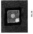
- FIG. 3Ais a photograph of a sidewall of a die cut by laser ablation shown at an intermediate cleaning step in accordance with a method of the present invention
- FIG. 3Bis a photograph of a top view of the die shown at the intermediate cleaning step of FIG. 3A;
- FIG. 3Cis a photograph of the sidewall of the die of FIG. 3A shown upon completion of cleaning;
- FIG. 3Dis a photograph of a top view of the die shown upon completion of cleaning of FIG. 3C
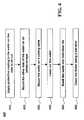
- FIG. 4shows an exemplary method of protecting and cleaning a wafer separated using laser cuts on a single side
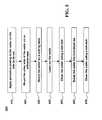
- FIG. 5shows another exemplary method of protecting and cleaning a wafer separated using laser cuts on a single side
- FIG. 6shows yet another exemplary method of protecting and cleaning a wafer separated using laser cuts on a single side
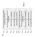
- FIG. 7shows an exemplary method of protecting and cleaning a wafer separated using laser cuts on each side
- FIG. 8shows another exemplary method of protecting and cleaning a wafer separated using laser cuts on each side.
- the present inventionrelates generally to an efficient process for die separation. Because of the large amount of energy needed to remove sapphire from a cut area using laser ablation, the waste sapphire tends to form a residue that cannot be removed easily. This waste, or slag, as it is commonly referred to, has two effects on subsequent die yield from the separation process. First, the top surface of the die has been found to have a large buildup of material around the perimeter of the die that degrades reliability and prevents wire bonding of the die. If the die size is generally less than 0.5 mm square, the entire surface can be covered by slag as illustrated by FIG. 1.
- the coating technology to protect the wafers from damage from the laser ablationshould be compatible with the sapphire wafer, adhesive tape, and cleaning solution.
- a laser separation system of the type suitable for the present inventionincludes a KrF laser with wavelength of 248 nm (nanometers), and maximum pulse energy of 400 mJ (millijoule), such as the IX-1000 laser workstation made by JP SERCEL ASSOCIATES, INC.
- any laser that has the power, wavelength and frequency, for die separationmay be used.
- Such lasersmay include, but are not limited to KrF lasers, Nd:YAG lasers.
- the process of the present inventionminimizes the steps required for conventional die separation system by using compatible materials.
- an exemplary method 400 for protecting and cleaning a semiconductor wafer separated using laser cuts on a single side of a semiconductor waferprotects the semiconductor wafer from slag (waste substrate) resulting from laser cutting and debris resulting from breaking the semiconductor wafer into die after the laser cutting.
- the waferincludes a sapphire substrate and a device layer.
- the device layerpreferably is a nitride layer such as gallium nitride (GaN), aluminum nitride, and indium nitride.
- the waferis applied with a protective coating to the side to be cut, i.e., the side facing the laser beam.
- the protective coatingprevents contamination from the slag resulting from the actual cutting process at step 440 .
- the waferis mounted with a mounting material.
- the mounting material in this and other methods described belowis an adhesive tape coated with a generally high tack adhesive. Note that the side not facing the laser beam is mounted on the adhesive tape.
- the waferis mounted on a cutting table, and is laser cut at step 440 using ablation.
- the cuttingmay deposit slag on the top of the semiconductor wafer and on both sides of each cut.
- the waferis broken into die using conventional methods such as roller breaking and 3-point bending.
- the waferremains on the adhesive tape during and after the breaking process.
- debris resulting from the breaking stepmay have been deposited on the wafer.
- the waferis cleaned using a wet etch.
- the cleaning solution used in the wet etch, the protective coating, and the adhesive tapeare selected in such a way that the cleaning solution removes the protective coating, the slag, and the debris, but does not damage the adhesive tape and the die.
- the cleaning solutionare solutions that include one or more of the following solvents: n-methyl pyrrolidone (NMP), dipropylene glycol monomethyl ether, polyglycol ether, tetrahydo thiophene dioxide, nonaqueous quaternary ammonium hydroxide, potassium borate, and potassium hydroxide (KOH).
- EKC-830includes NMP and Photoresist developer AZ400K includes both KOH and potassium borate.
- the protective coatingare photoresists utilizing an organic backbone comprised of cresol novolac resins such as photoresist AZ4330RS having diazonaphthoquinone sulfonic ester or trihydroxybenzophenone.
- An alternate useful organic backbone materialis polyhydroxystyrene.
- the adhesive tapeare conventional medium tack tapes such as P/N 18074-10.00 from SEMICONDUCTOR EQUIPMENT CORPORATION and conventional high tack tapes such as Type 1004R adhesive tape from ULTRON SYSTEMS.
- UV release tapemay be used.
- the preferred combinationis EKC-830, photoresist AZ4330RS, and a conventional medium tack tape for the cleaning solution, the protective coating, and the adhesive tape, respectively.
- EKC-830EKC-830
- photoresist AZ4330RSphotoresist AZ4330RS
- a conventional medium tack tapefor the cleaning solution, the protective coating, and the adhesive tape, respectively.
- a conventional medium tack tapecan be used as a protective coating as well.
- the protective coatingis not removed by the cleaning solution and is peeled off before or after the cleaning step.
- More than one medium tack tapecan be used as the protective coating during the dicing of the wafer. For example, after cutting the wafer in one direction, the medium tack tape is replaced with another before cutting the wafer in another direction.
- the cleaning stepcan also use a dry etch, or a dry etch followed by a wet etch. If a dry etch is used, the cleaning agent is not a cleaning solution. Rather, the cleaning agent is referred to as the plasma cleaning process.
- the preferred cleaning agent for a dry etchis the chlorine-based plasma.
- the preferred protective coating and adhesive tapeare photoresist AZ4330RS, and a conventional medium tack tape, respectively.
- One advantage of using a dry etch with a protective coatingis that the protective coating acts as a mask for the die. Thus, the dry etch effectively cleans the sidewalls without damaging the die. If only a dry etch is used and no wet etches follow, the debris and the protective coating would not be removed.
- the debriscan be removed by using solution such as KOH in a cleaning tank such as an ultrasonic tank, or solution such as EKC-830 in an ULTRA-T wafer cleaner.
- the protective coatingmay be removed in a similar manner. To avoid the additional effort for removing the debris and the protective coating, after a dry etch, a wet etch is applied.
- Method 400has the wafer broken up at step 450 before cleaning the wafer at step 460 .
- An advantage of the arrangementis that the slag and the debris are removed simultaneously. If the debris is not a concern, steps 450 and 460 can be reversed. That is, the cleaning step 460 is performed right after the cutting step 440 and before the breaking step 450 . In this exemplary case, the cleaning solution is not required to remove the debris resulting from the breaking step.
- the preferred cleaning solution, the protective coating, and the adhesive tapeare Photoresist developer AZ400K, photoresist AZ4330RS and a conventional medium tack tape, respectively. If a dry etch is used, the preferred combination of the cleaning agent, the protective coating, and the adhesive tape is the same as those stated previously.
- method 500which is an alternative to method 400 , is shown.
- the first four stepsare the same as those in method 400 and are labeled the same as in FIG. 4.
- method 500performs two cleaning steps.
- the first cleaning step(step 550 ) is performed after the cutting step 440 but before the breaking step 560 , so that the protective coating and the slag resulting from the cutting are removed.
- the second cleaning step(step 570 ) is performed after the breaking step 560 , so that debris resulting from the breaking is removed.
- the first and the second cleaning stepsare performed with a wet etch. They also can be performed with a dry etch, or a dry etch followed by a wet etch as well.
- the cleaning solution selected for the second cleaning stepcan be different from that selected for the first cleaning step.
- cleaning solutions selected for the first cleaning stepshould be able to remove the protective coating and the slag but do not need the capability for removing the debris, and those selected for the second cleaning step should remove the debris but do not need the capability to remove the slag or the protective coating.
- the solution selected for either stepshould not damage the adhesive tape and the die.
- the preferred protecting coating and the adhesive tapeare photoresist AZ4330RS and a conventional medium tack tape, respectively.
- a conventional medium tack tapecan also be used as the protective coating, and a conventional high tack tape can also be used as the adhesive tape.
- the preferred cleaning solutions used in the first and the second cleaning stepsare Photoresist developer AZ400K and EKC-830, respectively. It should be noted that KOH can also be used as the cleaning solution at the second cleaning step and that the solutions used in the second cleaning step can also be used in the first cleaning step.
- a dry etchis used, the preferred combination of the cleaning agent, the protective coating, and the adhesive tape is the same as those described for the method shown in FIG. 4.
- a wet etch with EKC-830 or KOHcan follow the dry etch.
- step 570can be omitted. Furthermore, if the cut is not a complete cut, step 420 can be done immediately before breaking step 560 , because cutting step 440 and cleaning step 550 do not require an adhesive tape to hold the wafer together.
- FIG. 6illustrative method 600 for protecting and cleaning a wafer separated using laser cut is shown.
- the first four stepsare the same as those in method 400 and are labeled the same as in FIG. 4.
- the waferis detached from the adhesive tape at step 650 and is cleaned with a cleaning solution using a wet etch at step 660 . Both steps 650 and 660 should not break the wafer.
- the slag resulting from cutting step 440 and the protective coatingare removed at step 660 .
- the waferis then re-mounted on the same adhesive tape at step 670 and is broken into die using conventional methods at step 680 .
- a second cleaning stepis then performed at step 690 to remove the debris resulting from the breaking step 680 .
- the method of cleaning in both steps 660 and 690is a wet etch but it can be a dry etch, or a dry etch followed by a wet etch.
- the cleaning solution for step 690can be different from step 660 .
- the cleaning solution for the first cleaning step (step 660 )is able to remove the protective coating and the slag but is not restricted to those types that do not damage the adhesive tape.
- the cleaning solution for step 690removes the debris but does not need the capability to remove the slag or the protective coating.
- the cleaning solution selected in the second step (step 690 )is of the type that does not damage the adhesive tape and the die.
- the preferred and other combinations of the cleaning agents in the two cleaning steps, the protective coating, and the adhesive tapeare the same as those respective steps described for the method shown in FIG. 5.
- Steps 410 and 420 in methods 400 , 500 , and 600can be done in any sequence.
- step 420can be done before step 410 , or both steps can be done simultaneously.
- the methods described so farhave been applicable to a wafer that is separated on one side using a laser beam (the single cut approach).
- the single cut approachmay cause the wafer to crack or produce more waste because of the depth of the cut.
- the depth of the saturation pointvaries based on the laser system and laser used, but is approximately 150• m (micrometer); the wafer thickness can be more than 150• m, generally, about 425• m.
- One way to solve the problemsis to make partial cuts on each side of the wafer (the double cut approach).
- An advantage of the double cut approachis that there is no need to thin the wafer; thus, the processing time is reduced and the efficiency is increased.
- cutting the wafer from the top and bottomresults in more uniform devices, as the break between the cut tends to stay closer to perpendicular to the wafer surfaces. Where high quality optical devices are desirable, the double cut approach may be preferable due to the just described break lines.
- FIG. 7shows an exemplary method 700 for wafer protection and cleaning when the double cut approach is used.
- the waferincludes a sapphire substrate and the laser separation is accomplished using laser ablation.
- first and second protective coatingsare applied to respective sides of the wafer.
- the side to be cut firstis called the first side and the other side, the second side.
- the first sideis the substrate side.
- the first sideusually is not the side that is faced up for subsequent packaging to avoid the additional effort of re-mounting.
- the second side of the sapphireis mounted on an adhesive tape with the first side facing the laser beam, and the wafer is then mounted on a cutting table at step 730 .
- the waferis cut on the first side and the wafer is then cleaned with a wet etch at step 750 .
- the cleaning solution selected at step 750should remove the first protective coating from the first side and the slag generated at step 740 , but should not damage the adhesive tape and the die.
- the second protective coatingeven if it is the same type as the first protective coating, is not damaged by step 740 because it is positioned against the adhesive tape. This selection of the cleaning solution, the adhesive tape, and the first and second protective coatings minimizes the handling and process time in the lab. Without this selection, further cleaning on the first side would be impossible prior to packaging.
- the waferis detached from the adhesive tape, and the first side of the wafer is then mounted on the adhesive tape at step 770 , i.e., the second side faces the laser beam.
- the second side of the waferis then cut at step 780 , and broken into die using conventional methods, as at step 790 .
- the waferis cleaned again using at least a wet etch with a different cleaning solution, as at step 795 .
- the cleaning solution used at step 795should remove the slag produced at step 780 , the debris produced at step 790 , and the second protective coating, but it should not damage the adhesive tape and the die.
- the preferred and other cleaning agents for the first (step 750 ) and the second (step 795 ) cleaning stepsare the same as those described for the respective steps in FIG. 5.
- the preferred and other adhesive tapesare also the same as those disclosed for the method shown in FIG. 5.
- Photoresist AZ4330RSis preferred for both protective coatings, although a conventional medium tack tape can be used as well, and the two protective coatings can be different.
- step 795it is preferred that at the second cleaning step (step 795 ), two wet etches are used.
- the cleaning solutions used in these two wet etchesare the same but they can be different.
- Both cleaning stepsmay involve a dry etch before a wet etch.
- cleaning step 795it is preferred that two wet etches follow the dry etch.
- steps 790 and 795can be reversed, and the cleaning solution selected at step 795 is not required to remove the debris.
- [0058] 740Laser cut wafer to a depth of 90 microns.
- FIG. 8illustrates method 800 incorporating this feature.
- the waferis mounted on the cutting table with the first side facing the laser as at step 820 .
- the waferis cut on the first side.
- the waferis re-mounted on the cutting table with the second side facing the laser, and, at step 850 , the wafer is cut on the second side.
- the second sideis, then, cleaned at the first cleaning step 860 .
- the second side of the waferis mounted on an adhesive tape, and, at step 880 , the wafer is broken into die.
- the first side of the waferis cleaned.
- the adhesive tape and the protective coatingssee method 700 .
- the preferred and other cleaning agents for steps 860 and 890see those described in method 700 for steps 795 and 750 , respectively.
- the first sidecan be cleaned at step 860 and the second side at step 890 .
- the wafershould be mounted on the cutting table with the first side facing the laser before step 860 and, at step 870 , the first side should be mounted with the adhesive tape.
- both first and second sidescan be cleaned and, at step 870 , the wafer is mounted on the adhesive tape on either side for broken into die at step 880 .
- step 890can be omitted or be used for more cleaning if the wafer is still dirty.
- ultrasonic agitation or megasonic agitationcan be incorporated as part of the wet etch.
- the sonic wavebreaks up the protective coating and slag that has stuck to the wafer, making the protective coating and the slag easier to be dissolved by the cleaning solution.
- An advantage of ultrasonic or megasonic processingis that the processing improves the efficiency of the cleaning without damaging the wafer.
- the epitaxial growth materialcan be, for example, any semiconductor material such as any of the III-V materials listed in the periodic chart of elements.
- the substrate materialcan be, for example, silicon, any of the III-V materials, refractory ceramics and any orientations of any of the listed substrate materials.
- KOHshould be used as the cleaning solution.
- all cleaning agents disclosed previouslycan be used.
- the waferis mounted on a pedestal and mounting tape is not used.
- the pedestalholds the wafer for cutting by the laser, and permits the wafer to be cut to its periphery.
- Some protective coatingis applied prior to mounting on the pedestal.
- the waferis removed and cleaned.
- the cut, cleaned waferis then placed on mounting tape and broken.
- the waferis then optionally cleaned, preferably using a cleaning agent that does not degrade the tape.
Landscapes
- Physics & Mathematics (AREA)
- Engineering & Computer Science (AREA)
- Optics & Photonics (AREA)
- Plasma & Fusion (AREA)
- Mechanical Engineering (AREA)
- General Physics & Mathematics (AREA)
- Condensed Matter Physics & Semiconductors (AREA)
- Manufacturing & Machinery (AREA)
- Computer Hardware Design (AREA)
- Microelectronics & Electronic Packaging (AREA)
- Power Engineering (AREA)
- Dicing (AREA)
- Laser Beam Processing (AREA)
- Led Devices (AREA)
Abstract
Description
- This application is a continuation-in-part of co-pending U.S. patent application Ser. No. 09/178,287, entitled “SEMICONDUCTOR DEVICE SEPARATION USING A PATTERNED LASER PROJECTION,” filed Oct. 23, 1998. This application is also related to co-pending U.S. patent application Ser. No. ______, (Emcore 6) entitled “SEMICONDUCTOR DEVICE SEPARATION USING A PATTERNED LASER PROJECTION,” filed February ______, 2002.[0001]
- This invention relates to the field of semiconductor fabrication, and more particularly to semiconductor device separation.[0002]
- In the field of semiconductor device fabrication, there are various methods for separating a wafer into die, including scribe and break techniques. In scribe and break techniques, the die is separated by breaking the wafer along scribe lines, which can be cut in the wafer in a number of ways. For example, wafers having semiconductor substrates can be mechanically scribed, such as with a diamond. In wafers having sapphire substrates, laser scribing has been disclosed, as, for example, in U.S. patent application Ser. No. 09/178.287, entitled, “Semiconductor Device Separation Using a Patterned Laser Projection,” which is incorporated herein by reference. The device separation method disclosed therein uses laser ablation to form scribe lines in the wafer.[0003]
- Because scribing removes material from the wafer, some scribing techniques can result in the buildup of waste material on the wafer. In laser ablation scribing, for example, waste substrate material, also referred to as slag, tends to form as residue on the wafer. The slag forms on the sidewall and around the die perimeter, building from the bottom of the cut to the top. That is, there tends to be more slag near the top of the cut than the bottom. Slag around the die perimeter can degrade the reliability of the device and inhibit wire bonding. In optical devices, such as LED's and lasers, sidewall buildup can decrease the power output of the device, as the slag can absorb some of the optical output power of the device.[0004]
- It has been suggested that a protective coating of a photoresist material can be used to protect the topside of the die from waste material. The material is applied and then cured to form the protective coating. The coating, of course, must be removed at some point in the separation process, such as by using a solvent. Known uses of photoresist protective coating techniques tend to decrease process times as additional activities or steps must be carried out in the separation process. In device fabrication, processes that deliver high yields in short times are desirable, as even relatively minor increases in efficiency can lead to significant increases in device throughput.[0005]
- A method according to the principles of the present invention provides for efficient device separation processing by using compatible materials. In one aspect, processing steps are minimized by choosing compatible materials for mounting the wafer, protecting the devices and cleaning off the protective coating. In one embodiment, the method includes the step of applying a protective coating on the side to be cut of a semiconductor wafer, mounting the other side of the semiconductor wafer on a mounting material such as an adhesive tape, cutting the semiconductor with a laser beam, and cleaning the wafer with a cleaning agent. The mounting material, the cleaning agent, and the protective coating are selected such that the cleaning agent does not damage the mounting material but removes the protective coating. Specifically, when an adhesive tape is used as the mounting material, the cleaning agent does not damage the adhesive and the tape forming the adhesive tape. As a result, the semiconductor wafer remains on the mounting material during and after the cleaning process, increasing the efficiency of the process.[0006]
- In another exemplary embodiment, the method of the invention includes the following steps: applying a protective coating on the side to be cut of a wafer with sapphire substrate, mounting the other side of the wafer on an adhesive tape, mounting the wafer with the adhesive tape on a cutting table, cutting the wafer with a laser, breaking the wafer into die, and cleaning the wafer by a wet etch with a cleaning solution. The cleaning solution, the protective coating, and the adhesive tape are selected such that the cleaning solution removes slag resulting from the cutting, debris resulting from the breaking, and the protective coating, but does not damage the adhesive tape, so that the die can remain on the adhesive tape before, during and after the cleaning.[0007]
- A more complete understanding of the invention may be obtained from consideration of the following description in conjunction with the drawings in which:[0008]
- FIG. 1 is a photograph of a die cut by laser ablation covered with a deposit of slag;[0009]
- FIG. 2 is a photograph of a wafer cut into die by laser ablation and covered with a deposit of slag;[0010]
- FIG. 3A is a photograph of a sidewall of a die cut by laser ablation shown at an intermediate cleaning step in accordance with a method of the present invention;[0011]
- FIG. 3B is a photograph of a top view of the die shown at the intermediate cleaning step of FIG. 3A;[0012]
- FIG. 3C is a photograph of the sidewall of the die of FIG. 3A shown upon completion of cleaning;[0013]
- FIG. 3D is a photograph of a top view of the die shown upon completion of cleaning of FIG. 3C[0014]
- FIG. 4 shows an exemplary method of protecting and cleaning a wafer separated using laser cuts on a single side;[0015]
- FIG. 5 shows another exemplary method of protecting and cleaning a wafer separated using laser cuts on a single side;[0016]
- FIG. 6 shows yet another exemplary method of protecting and cleaning a wafer separated using laser cuts on a single side;[0017]
- FIG. 7 shows an exemplary method of protecting and cleaning a wafer separated using laser cuts on each side; and[0018]
- FIG. 8 shows another exemplary method of protecting and cleaning a wafer separated using laser cuts on each side.[0019]
- With reference to the figures for purposes of illustration, the present invention relates generally to an efficient process for die separation. Because of the large amount of energy needed to remove sapphire from a cut area using laser ablation, the waste sapphire tends to form a residue that cannot be removed easily. This waste, or slag, as it is commonly referred to, has two effects on subsequent die yield from the separation process. First, the top surface of the die has been found to have a large buildup of material around the perimeter of the die that degrades reliability and prevents wire bonding of the die. If the die size is generally less than 0.5 mm square, the entire surface can be covered by slag as illustrated by FIG. 1. Secondly, sidewalls of the die which are exposed during ablation have a slag buildup that increases from the bottom to the top of the cut. This excess material decreases the output power of the die since it is absorbing. Given that the comparable hardness of the diamond, used in conventional scribing and dicing saw tools, and the sapphire make traditional separation processes very inefficient, experiments were conducted to discovers techniques to improve the die yield.[0020]
- The experiments were conducted using a 248 nm KrF excimer laser on wafers composed of GaN/sapphire and sapphire that made cut depths in the range of 1 to 6 mil on one or both sides of the wafer. The kerf width was a maximum of 4 mil with sharp edges as illustrated in FIG. 1. An example of a whole wafer cut with the laser is illustrated in FIG. 2. The series of experiments were directed at discovering ways to improve die yields while minimizing the number of steps required for separation. The following approaches were attempted during the die separation process and each resulted in an improvement of the die yield:[0021]
- a. variations on applying to the front surface of the wafer a protective coating;[0022]
- b. variations on applying to the back surface of the wafer a protective coating;[0023]
- c. variations on applying and removing an adhesive tape on the side of the wafer facing away from the laser;[0024]
- d. variations on cleaning the die using a wet chemical etch to remove the protective coating and clean the side walls of the die;[0025]
- e. variations on cleaning the die using a dry etch to remove the protective coating and clean the side walls of the die; and[0026]
- f. variations on using a sonic bath using ultrasonic and megasonic frequencies for the wet chemical etching to accelerate and improve the cleaning efficiency.[0027]
- During these experiments, yield improvements were attained while varying each of the above approaches. Advantageously, an unexpected result of these experiments was the discovery that, while each of these approaches can be varied to improve yield rates, the existence of certain interdependencies in the process steps and compatibility between certain materials obtained greater yield rates. Such yield rates were not obtained when these interdependencies and compatibilities did not exist. This discovery means that higher yield rates can be obtained while allowing for manufacturers to mix and match their process steps as may be desirable when varying, by way of example not by limitation, the device structure thickness, surface morphology and size.[0028]
- It will be understood by one of ordinary skill in art that the interdependencies and compatibilities described herein can be used to develop critical process protocols tailored to particular separation systems and desired end products. From the above experiments, the following interdependencies and compatibilities were discovered:[0029]
- 1. The coating technology to protect the wafers from damage from the laser ablation should be compatible with the sapphire wafer, adhesive tape, and cleaning solution.[0030]
- 2. The cleaning steps of a wet chemical etch and a dry etch are interchangeable and/or may be used in combination. When used in combination, more sidewall slag was removed from the edge of the die and improved efficiency in the die was observed.[0031]
- The consideration of either or both of these features was found to have improved yield rates. Furthermore by practicing these principles, it was discovered that separation processes including the steps of protecting at least one surface of the wafer with a coating, applying an adhesive tape compatible with the desired cleaning solution, and using a dry etch and/or wet etch in ultrasonic to clean the surfaces were now feasible. The flexibility and the ease of use of these process steps permit a manufacturer to quickly and inexpensively separate die in any manufacturing program while producing a finished product free of surface or sidewall contamination and increasing yield while at the same time creating higher efficiency die. With reference to FIGS.[0032]3A-D, an actual die was obtained relatively free of slag in accordance with the method illustrated in FIG. 7 discussed in greater detail below. The die was photographed for FIGS. 3A and 3B during an intermediate cleaning step and photographed for FIGS. 3C and 3D upon completion of the method of FIG. 7. While these discoveries are particularly well suited for wafers based on a sapphire substrate undergoing separation by laser ablation, these results are not intended to limited to such wafers and separation techniques. The application of these techniques in exemplary die separation processes are more fully set forth below.
- By way of example, and not by limitation, the exemplary processes of the present invention are described utilizing a conventional laser-separation system. However, those skilled in the art will appreciate that any conventional wafer cutting tool system such as dicing saw or scribe-break systems may substitute for the laser. A laser separation system of the type suitable for the present invention includes a KrF laser with wavelength of 248 nm (nanometers), and maximum pulse energy of 400 mJ (millijoule), such as the IX-1000 laser workstation made by JP SERCEL ASSOCIATES, INC. However, any laser that has the power, wavelength and frequency, for die separation may be used. Such lasers may include, but are not limited to KrF lasers, Nd:YAG lasers. Advantageously, the process of the present invention minimizes the steps required for conventional die separation system by using compatible materials.[0033]
- Referring to FIG. 4, an[0034]
exemplary method 400 for protecting and cleaning a semiconductor wafer separated using laser cuts on a single side of a semiconductor wafer. Themethod 400 protects the semiconductor wafer from slag (waste substrate) resulting from laser cutting and debris resulting from breaking the semiconductor wafer into die after the laser cutting. For illustration purposes, the wafer includes a sapphire substrate and a device layer. However, any substrate and device layer combination can be used without departing from the principles of the invention. The device layer preferably is a nitride layer such as gallium nitride (GaN), aluminum nitride, and indium nitride. Atstep 410, the wafer is applied with a protective coating to the side to be cut, i.e., the side facing the laser beam. The protective coating prevents contamination from the slag resulting from the actual cutting process atstep 440. Atstep 420, the wafer is mounted with a mounting material. For illustration purposes, the mounting material in this and other methods described below is an adhesive tape coated with a generally high tack adhesive. Note that the side not facing the laser beam is mounted on the adhesive tape. Atstep 430, the wafer is mounted on a cutting table, and is laser cut atstep 440 using ablation. - The cutting may deposit slag on the top of the semiconductor wafer and on both sides of each cut. At[0035]
step 450, the wafer is broken into die using conventional methods such as roller breaking and 3-point bending. Advantageously, the wafer remains on the adhesive tape during and after the breaking process. At this point, in addition to the slag, debris resulting from the breaking step may have been deposited on the wafer. - At[0036]
step 460, the wafer is cleaned using a wet etch. In accordance with the principles of the invention, the cleaning solution used in the wet etch, the protective coating, and the adhesive tape are selected in such a way that the cleaning solution removes the protective coating, the slag, and the debris, but does not damage the adhesive tape and the die. Examples of the cleaning solution are solutions that include one or more of the following solvents: n-methyl pyrrolidone (NMP), dipropylene glycol monomethyl ether, polyglycol ether, tetrahydo thiophene dioxide, nonaqueous quaternary ammonium hydroxide, potassium borate, and potassium hydroxide (KOH). For example, EKC-830 includes NMP and Photoresist developer AZ400K includes both KOH and potassium borate. Examples of the protective coating are photoresists utilizing an organic backbone comprised of cresol novolac resins such as photoresist AZ4330RS having diazonaphthoquinone sulfonic ester or trihydroxybenzophenone. An alternate useful organic backbone material is polyhydroxystyrene. Examples of the adhesive tape are conventional medium tack tapes such as P/N 18074-10.00 from SEMICONDUCTOR EQUIPMENT CORPORATION and conventional high tack tapes such as Type 1004R adhesive tape from ULTRON SYSTEMS. Also, UV release tape may be used. Although any combination of the above can be used, the preferred combination is EKC-830, photoresist AZ4330RS, and a conventional medium tack tape for the cleaning solution, the protective coating, and the adhesive tape, respectively. Advantageously, such a selection enables the wafer to remain on the adhesive tape during and after the cleaning step, increasing the efficiency of the separation process. - A conventional medium tack tape can be used as a protective coating as well. In this case, the protective coating is not removed by the cleaning solution and is peeled off before or after the cleaning step. More than one medium tack tape can be used as the protective coating during the dicing of the wafer. For example, after cutting the wafer in one direction, the medium tack tape is replaced with another before cutting the wafer in another direction.[0037]
- The cleaning step can also use a dry etch, or a dry etch followed by a wet etch. If a dry etch is used, the cleaning agent is not a cleaning solution. Rather, the cleaning agent is referred to as the plasma cleaning process. The preferred cleaning agent for a dry etch is the chlorine-based plasma. The preferred protective coating and adhesive tape are photoresist AZ4330RS, and a conventional medium tack tape, respectively. One advantage of using a dry etch with a protective coating is that the protective coating acts as a mask for the die. Thus, the dry etch effectively cleans the sidewalls without damaging the die. If only a dry etch is used and no wet etches follow, the debris and the protective coating would not be removed. In this case, the debris can be removed by using solution such as KOH in a cleaning tank such as an ultrasonic tank, or solution such as EKC-830 in an ULTRA-T wafer cleaner. The protective coating may be removed in a similar manner. To avoid the additional effort for removing the debris and the protective coating, after a dry etch, a wet etch is applied.[0038]
- [0039]
Method 400 has the wafer broken up atstep 450 before cleaning the wafer atstep 460. An advantage of the arrangement is that the slag and the debris are removed simultaneously. If the debris is not a concern, steps450 and460 can be reversed. That is, the cleaningstep 460 is performed right after the cuttingstep 440 and before the breakingstep 450. In this exemplary case, the cleaning solution is not required to remove the debris resulting from the breaking step. The preferred cleaning solution, the protective coating, and the adhesive tape are Photoresist developer AZ400K, photoresist AZ4330RS and a conventional medium tack tape, respectively. If a dry etch is used, the preferred combination of the cleaning agent, the protective coating, and the adhesive tape is the same as those stated previously. - If the laser cut is not a complete cut, another change that can be made to[0040]
method 400 is to perform adhesivetape mounting step 420 immediately before breakingstep 450. This is because the wafer remains together without the help of a adhesive mounting tape during and after cuttingstep 440, but to keep the wafer together during and after breakingstep 450, the adhesive tape is preferred. - Referring now to FIG. 5,[0041]
illustrative method 500, which is an alternative tomethod 400, is shown. The first four steps are the same as those inmethod 400 and are labeled the same as in FIG. 4. Instead of performing one cleaning step,method 500 performs two cleaning steps. The first cleaning step (step550) is performed after the cuttingstep 440 but before the breakingstep 560, so that the protective coating and the slag resulting from the cutting are removed. Whereas the second cleaning step (step570) is performed after the breakingstep 560, so that debris resulting from the breaking is removed. The first and the second cleaning steps are performed with a wet etch. They also can be performed with a dry etch, or a dry etch followed by a wet etch as well. The cleaning solution selected for the second cleaning step can be different from that selected for the first cleaning step. - In accordance with the principles of the invention, cleaning solutions selected for the first cleaning step should be able to remove the protective coating and the slag but do not need the capability for removing the debris, and those selected for the second cleaning step should remove the debris but do not need the capability to remove the slag or the protective coating. The solution selected for either step should not damage the adhesive tape and the die. The preferred protecting coating and the adhesive tape are photoresist AZ4330RS and a conventional medium tack tape, respectively. A conventional medium tack tape can also be used as the protective coating, and a conventional high tack tape can also be used as the adhesive tape. The preferred cleaning solutions used in the first and the second cleaning steps are Photoresist developer AZ400K and EKC-830, respectively. It should be noted that KOH can also be used as the cleaning solution at the second cleaning step and that the solutions used in the second cleaning step can also be used in the first cleaning step.[0042]
- If a dry etch is used, the preferred combination of the cleaning agent, the protective coating, and the adhesive tape is the same as those described for the method shown in FIG. 4. To also remove the debris and the protective coating, at the second cleaning step, a wet etch with EKC-830 or KOH can follow the dry etch.[0043]
- If the debris is not a concern,[0044]
step 570 can be omitted. Furthermore, if the cut is not a complete cut,step 420 can be done immediately before breakingstep 560, because cuttingstep 440 and cleaningstep 550 do not require an adhesive tape to hold the wafer together. - Referring now to FIG. 6,[0045]
illustrative method 600 for protecting and cleaning a wafer separated using laser cut is shown. The first four steps are the same as those inmethod 400 and are labeled the same as in FIG. 4. After cuttingstep 440, the wafer is detached from the adhesive tape atstep 650 and is cleaned with a cleaning solution using a wet etch atstep 660. Bothsteps step 440 and the protective coating are removed atstep 660. The wafer is then re-mounted on the same adhesive tape atstep 670 and is broken into die using conventional methods atstep 680. A second cleaning step is then performed atstep 690 to remove the debris resulting from the breakingstep 680. The method of cleaning in bothsteps step 690 can be different fromstep 660. The cleaning solution for the first cleaning step (step660) is able to remove the protective coating and the slag but is not restricted to those types that do not damage the adhesive tape. The cleaning solution forstep 690 removes the debris but does not need the capability to remove the slag or the protective coating. The cleaning solution selected in the second step (step690) is of the type that does not damage the adhesive tape and the die. The preferred and other combinations of the cleaning agents in the two cleaning steps, the protective coating, and the adhesive tape are the same as those respective steps described for the method shown in FIG. 5. - [0046]
Steps methods step 410, or both steps can be done simultaneously. - The methods described so far have been applicable to a wafer that is separated on one side using a laser beam (the single cut approach). For a thick wafer, the single cut approach may cause the wafer to crack or produce more waste because of the depth of the cut. Furthermore, there is a saturation point on each side of the wafer that limits the cut depth. The depth of the saturation point varies based on the laser system and laser used, but is approximately 150• m (micrometer); the wafer thickness can be more than 150• m, generally, about 425• m. One way to solve the problems is to make partial cuts on each side of the wafer (the double cut approach). An advantage of the double cut approach is that there is no need to thin the wafer; thus, the processing time is reduced and the efficiency is increased. Also, cutting the wafer from the top and bottom results in more uniform devices, as the break between the cut tends to stay closer to perpendicular to the wafer surfaces. Where high quality optical devices are desirable, the double cut approach may be preferable due to the just described break lines.[0047]
- FIG. 7 shows an[0048]
exemplary method 700 for wafer protection and cleaning when the double cut approach is used. Again, for illustration purposes, the wafer includes a sapphire substrate and the laser separation is accomplished using laser ablation. - At[0049]
step 710, first and second protective coatings are applied to respective sides of the wafer. Here, the side to be cut first is called the first side and the other side, the second side. Preferably, the first side is the substrate side. The first side usually is not the side that is faced up for subsequent packaging to avoid the additional effort of re-mounting. - At[0050]
step 720, the second side of the sapphire is mounted on an adhesive tape with the first side facing the laser beam, and the wafer is then mounted on a cutting table atstep 730. Atstep 740, the wafer is cut on the first side and the wafer is then cleaned with a wet etch atstep 750. In accordance with the principles of the invention, the cleaning solution selected atstep 750 should remove the first protective coating from the first side and the slag generated atstep 740, but should not damage the adhesive tape and the die. The second protective coating, even if it is the same type as the first protective coating, is not damaged bystep 740 because it is positioned against the adhesive tape. This selection of the cleaning solution, the adhesive tape, and the first and second protective coatings minimizes the handling and process time in the lab. Without this selection, further cleaning on the first side would be impossible prior to packaging. - At[0051]
step 760, the wafer is detached from the adhesive tape, and the first side of the wafer is then mounted on the adhesive tape atstep 770, i.e., the second side faces the laser beam. The second side of the wafer is then cut atstep 780, and broken into die using conventional methods, as atstep 790. The wafer is cleaned again using at least a wet etch with a different cleaning solution, as atstep 795. In accordance with the principles of the invention, the cleaning solution used atstep 795 should remove the slag produced atstep 780, the debris produced atstep 790, and the second protective coating, but it should not damage the adhesive tape and the die. The preferred and other cleaning agents for the first (step750) and the second (step795) cleaning steps are the same as those described for the respective steps in FIG. 5. The preferred and other adhesive tapes are also the same as those disclosed for the method shown in FIG. 5. Photoresist AZ4330RS is preferred for both protective coatings, although a conventional medium tack tape can be used as well, and the two protective coatings can be different. - Furthermore, it is preferred that at the second cleaning step (step[0052]795), two wet etches are used. The cleaning solutions used in these two wet etches are the same but they can be different.
- Both cleaning steps may involve a dry etch before a wet etch. For cleaning[0053]
step 795, it is preferred that two wet etches follow the dry etch. As inmethod 400, if the debris is not a concern, steps790 and795 can be reversed, and the cleaning solution selected atstep 795 is not required to remove the debris. - As discussed above the die shown in FIG. 3 was produced according to the method of FIG. 7 as follows:[0054]
- [0055]710—Coat both sides of wafer with photoresist.
- [0056]720—Mount the frontside of wafer medium tack tape.
- [0057]730—Mount wafer on table.
- [0058]740—Laser cut wafer to a depth of 90 microns.
- [0059]750—Cleaned the wafer with a wet etch.
- [0060]760—De-mount the wafer from the tape.
- [0061]770—Mount the backside of wafer on high tack tape.
- [0062]780—Laser cut wafer to a depth of 120 microns.
- [0063]790—Break wafer with a roller into individual die.
- [0064]795'—Cleaned the wafer with a wet etch with AZ400K+EKC-830. The photos of FIGS. 3 and 3B were taken upon completion of this intermediate cleaning step.
- [0065]795″—Cleaned the wafer with a wet etch of KOH and ultrasonic. The photos of FIGS. 3C and 3D were taken upon completion of cleaning.
- The step of mounting a wafer on an adhesive tape can be deferred until the wafer is ready to be broken into die. FIG. 8 illustrates[0066]
method 800 incorporating this feature. After applying first and second sides with respective coatings atstep 810, the wafer is mounted on the cutting table with the first side facing the laser as atstep 820. Atstep 830, the wafer is cut on the first side. Atstep 840, the wafer is re-mounted on the cutting table with the second side facing the laser, and, atstep 850, the wafer is cut on the second side. The second side is, then, cleaned at thefirst cleaning step 860. Atstep 870, the second side of the wafer is mounted on an adhesive tape, and, atstep 880, the wafer is broken into die. Atstep 890, the first side of the wafer is cleaned. For the preferred and other selections of the adhesive tape and the protective coatings, seemethod 700. For the preferred and other cleaning agents forsteps method 700 forsteps - In one embodiment, the first side can be cleaned at[0067]
step 860 and the second side atstep 890. In this embodiment, the wafer should be mounted on the cutting table with the first side facing the laser beforestep 860 and, atstep 870, the first side should be mounted with the adhesive tape. - Furthermore, at[0068]
step 860, both first and second sides can be cleaned and, atstep 870, the wafer is mounted on the adhesive tape on either side for broken into die atstep 880. In this embodiment, step890 can be omitted or be used for more cleaning if the wafer is still dirty. - In the methods described above, if EKC-830 or KOH is used at a cleaning step using a wet etch, ultrasonic agitation or megasonic agitation can be incorporated as part of the wet etch. The sonic wave breaks up the protective coating and slag that has stuck to the wafer, making the protective coating and the slag easier to be dissolved by the cleaning solution. An advantage of ultrasonic or megasonic processing is that the processing improves the efficiency of the cleaning without damaging the wafer.[0069]
- Although the above description primarily refers to cutting gallium nitride (GaN) on C-plane sapphire, these are only illustrative materials. The epitaxial growth material can be, for example, any semiconductor material such as any of the III-V materials listed in the periodic chart of elements. The substrate material can be, for example, silicon, any of the III-V materials, refractory ceramics and any orientations of any of the listed substrate materials. When any of the III-V materials is used as the substrate and a wet etch is used, KOH should be used as the cleaning solution. For other substrate materials, all cleaning agents disclosed previously can be used.[0070]
- In another embodiment, the wafer is mounted on a pedestal and mounting tape is not used. The pedestal holds the wafer for cutting by the laser, and permits the wafer to be cut to its periphery. Some protective coating is applied prior to mounting on the pedestal. After the laser is applied, the wafer is removed and cleaned. The cut, cleaned wafer is then placed on mounting tape and broken. The wafer is then optionally cleaned, preferably using a cleaning agent that does not degrade the tape.[0071]
- In accordance with the invention, methods for protecting and cleaning a semiconductor wafer separated using laser are described. Numerous modifications and alternative embodiments of the invention will be apparent to those skilled in the art in view of the foregoing description. Accordingly, this description is to be construed as illustrative only and is for the purpose of teaching those skilled in the art the best mode of carrying out the invention. Details of the structure and the procedure may be varied substantially without departing from the spirit of the invention and the exclusive use of all modifications which come within the scope of the appended claim is reserved.[0072]
Claims (79)
Priority Applications (1)
| Application Number | Priority Date | Filing Date | Title |
|---|---|---|---|
| US10/137,904US6849524B2 (en) | 1998-10-23 | 2002-05-02 | Semiconductor wafer protection and cleaning for device separation using laser ablation |
Applications Claiming Priority (2)
| Application Number | Priority Date | Filing Date | Title |
|---|---|---|---|
| US09/178,287US6413839B1 (en) | 1998-10-23 | 1998-10-23 | Semiconductor device separation using a patterned laser projection |
| US10/137,904US6849524B2 (en) | 1998-10-23 | 2002-05-02 | Semiconductor wafer protection and cleaning for device separation using laser ablation |
Related Parent Applications (1)
| Application Number | Title | Priority Date | Filing Date |
|---|---|---|---|
| US09/178,287Continuation-In-PartUS6413839B1 (en) | 1998-10-23 | 1998-10-23 | Semiconductor device separation using a patterned laser projection |
Publications (2)
| Publication Number | Publication Date |
|---|---|
| US20020127824A1true US20020127824A1 (en) | 2002-09-12 |
| US6849524B2 US6849524B2 (en) | 2005-02-01 |
Family
ID=22651952
Family Applications (5)
| Application Number | Title | Priority Date | Filing Date |
|---|---|---|---|
| US09/178,287Expired - LifetimeUS6413839B1 (en) | 1998-10-23 | 1998-10-23 | Semiconductor device separation using a patterned laser projection |
| US10/114,099Expired - LifetimeUS6902990B2 (en) | 1998-10-23 | 2002-04-02 | Semiconductor device separation using a patterned laser projection |
| US10/137,904Expired - LifetimeUS6849524B2 (en) | 1998-10-23 | 2002-05-02 | Semiconductor wafer protection and cleaning for device separation using laser ablation |
| US10/146,267AbandonedUS20030003690A1 (en) | 1998-10-23 | 2002-05-15 | Semiconductor device separation using a patterned laser projection |
| US10/845,790AbandonedUS20050003634A1 (en) | 1998-10-23 | 2004-05-13 | Semiconductor device separation using a patterned laser projection |
Family Applications Before (2)
| Application Number | Title | Priority Date | Filing Date |
|---|---|---|---|
| US09/178,287Expired - LifetimeUS6413839B1 (en) | 1998-10-23 | 1998-10-23 | Semiconductor device separation using a patterned laser projection |
| US10/114,099Expired - LifetimeUS6902990B2 (en) | 1998-10-23 | 2002-04-02 | Semiconductor device separation using a patterned laser projection |
Family Applications After (2)
| Application Number | Title | Priority Date | Filing Date |
|---|---|---|---|
| US10/146,267AbandonedUS20030003690A1 (en) | 1998-10-23 | 2002-05-15 | Semiconductor device separation using a patterned laser projection |
| US10/845,790AbandonedUS20050003634A1 (en) | 1998-10-23 | 2004-05-13 | Semiconductor device separation using a patterned laser projection |
Country Status (2)
| Country | Link |
|---|---|
| US (5) | US6413839B1 (en) |
| TW (1) | TW521334B (en) |
Cited By (31)
| Publication number | Priority date | Publication date | Assignee | Title |
|---|---|---|---|---|
| US6602762B2 (en)* | 2001-07-05 | 2003-08-05 | Chipbond Technology Corporation | System and method of laser sintering dies and dies sintered by laser sintering |
| US20050263854A1 (en)* | 1998-10-23 | 2005-12-01 | Shelton Bryan S | Thick laser-scribed GaN-on-sapphire optoelectronic devices |
| US20060157191A1 (en)* | 2005-01-14 | 2006-07-20 | Naoyuki Matsuo | Manufacturing method of laser processed parts and adhesive sheet for laser processing |
| US20060228650A1 (en)* | 2005-01-14 | 2006-10-12 | Naoyuki Matsuo | Manufacturing method of laser processed parts and protective sheet for laser processing |
| US20060246279A1 (en)* | 2003-04-25 | 2006-11-02 | Masakatsu Urairi | Method of producing laser-processed product and adhesive sheet, for laser processing used therefor |
| US20070007526A1 (en)* | 2005-07-08 | 2007-01-11 | Saori Sugiyama | Display panel and display device |
| US20070023136A1 (en)* | 2005-07-29 | 2007-02-01 | Priewasser Karl H | Method for processing a semiconductor wafer |
| US20070123061A1 (en)* | 2005-11-25 | 2007-05-31 | Advanced Laser Separation International B.V. | Method of treating a substrate, method of processing a substrate using a laser beam, and arrangement |
| US20070161211A1 (en)* | 2006-01-06 | 2007-07-12 | Masahiro Sunohara | Method for manufacturing semiconductor device |
| US20070181543A1 (en)* | 2003-12-25 | 2007-08-09 | Masakatsu Urairi | Protective sheet for laser processing and manufacturing method of laser processed parts |
| US20100078418A1 (en)* | 2008-09-26 | 2010-04-01 | Electro Scientific Industries, Inc. | Method of laser micro-machining stainless steel with high cosmetic quality |
| WO2011037921A1 (en)* | 2009-09-22 | 2011-03-31 | First Solar, Inc. | System and method for tracking and removing coating from an edge of a substrate |
| US20120115308A1 (en)* | 2010-11-05 | 2012-05-10 | Hua Chang-Huang | Fabrication method for dicing of semiconductor wafers using laser cutting techniques |
| US20120135553A1 (en)* | 2011-11-23 | 2012-05-31 | Soraa, Inc. | Method for Manufacture of Bright GaN LEDs Using a Selective Removal Process |
| US8778780B1 (en)* | 2005-10-13 | 2014-07-15 | SemiLEDs Optoelectronics Co., Ltd. | Method for defining semiconductor devices |
| US8946865B2 (en) | 2011-01-24 | 2015-02-03 | Soraa, Inc. | Gallium—nitride-on-handle substrate materials and devices and method of manufacture |
| US8994033B2 (en) | 2013-07-09 | 2015-03-31 | Soraa, Inc. | Contacts for an n-type gallium and nitrogen substrate for optical devices |
| US9076926B2 (en) | 2011-08-22 | 2015-07-07 | Soraa, Inc. | Gallium and nitrogen containing trilateral configuration for optical devices |
| US9105806B2 (en) | 2009-03-09 | 2015-08-11 | Soraa, Inc. | Polarization direction of optical devices using selected spatial configurations |
| US9287175B2 (en) | 2010-11-05 | 2016-03-15 | Win Semiconductors Corp. | Fabrication method for dicing of semiconductor wafers using laser cutting techniques |
| CN105405806A (en)* | 2014-09-09 | 2016-03-16 | 恩智浦有限公司 | Plasma Etching And Stealth Dicing Laser Process |
| CN105431252A (en)* | 2013-08-08 | 2016-03-23 | 奥斯兰姆奥普托半导体有限责任公司 | Method for dividing composite into semiconductor chips and semiconductor chips |
| US9419189B1 (en) | 2013-11-04 | 2016-08-16 | Soraa, Inc. | Small LED source with high brightness and high efficiency |
| US9450143B2 (en) | 2010-06-18 | 2016-09-20 | Soraa, Inc. | Gallium and nitrogen containing triangular or diamond-shaped configuration for optical devices |
| US9583678B2 (en) | 2009-09-18 | 2017-02-28 | Soraa, Inc. | High-performance LED fabrication |
| US9595636B2 (en) | 2012-03-28 | 2017-03-14 | Sensor Electronic Technology, Inc. | Light emitting device substrate with inclined sidewalls |
| US9646827B1 (en) | 2011-08-23 | 2017-05-09 | Soraa, Inc. | Method for smoothing surface of a substrate containing gallium and nitrogen |
| US9978904B2 (en) | 2012-10-16 | 2018-05-22 | Soraa, Inc. | Indium gallium nitride light emitting devices |
| US10096742B2 (en) | 2012-03-28 | 2018-10-09 | Sensor Electronic Technology, Inc. | Light emitting device substrate with inclined sidewalls |
| US10147850B1 (en) | 2010-02-03 | 2018-12-04 | Soraa, Inc. | System and method for providing color light sources in proximity to predetermined wavelength conversion structures |
| CN112122797A (en)* | 2020-09-24 | 2020-12-25 | 松山湖材料实验室 | Laser processing slag removal method, system, computer equipment and readable storage medium |
Families Citing this family (121)
| Publication number | Priority date | Publication date | Assignee | Title |
|---|---|---|---|---|
| JP4659300B2 (en) | 2000-09-13 | 2011-03-30 | 浜松ホトニクス株式会社 | Laser processing method and semiconductor chip manufacturing method |
| US6744072B2 (en)* | 2001-10-02 | 2004-06-01 | Xerox Corporation | Substrates having increased thermal conductivity for semiconductor structures |
| TWI326626B (en)* | 2002-03-12 | 2010-07-01 | Hamamatsu Photonics Kk | Laser processing method |
| WO2003076119A1 (en) | 2002-03-12 | 2003-09-18 | Hamamatsu Photonics K.K. | Method of cutting processed object |
| EP2400539B1 (en) | 2002-03-12 | 2017-07-26 | Hamamatsu Photonics K.K. | Substrate dividing method |
| KR101037142B1 (en)* | 2002-04-19 | 2011-05-26 | 일렉트로 사이언티픽 인더스트리즈, 아이엔씨 | Program-controlled dicing of substrate using pulse laser |
| US6960813B2 (en) | 2002-06-10 | 2005-11-01 | New Wave Research | Method and apparatus for cutting devices from substrates |
| US6806544B2 (en) | 2002-11-05 | 2004-10-19 | New Wave Research | Method and apparatus for cutting devices from conductive substrates secured during cutting by vacuum pressure |
| US6580054B1 (en) | 2002-06-10 | 2003-06-17 | New Wave Research | Scribing sapphire substrates with a solid state UV laser |
| US6995032B2 (en)* | 2002-07-19 | 2006-02-07 | Cree, Inc. | Trench cut light emitting diodes and methods of fabricating same |
| JP2004160483A (en)* | 2002-11-12 | 2004-06-10 | Disco Abrasive Syst Ltd | Laser processing method and laser processing apparatus |
| TWI520269B (en) | 2002-12-03 | 2016-02-01 | Hamamatsu Photonics Kk | Cutting method of semiconductor substrate |
| DE60311678T2 (en)* | 2002-12-20 | 2007-11-22 | Cree, Inc. | METHOD FOR PRODUCING SEMICONDUCTOR DEVICES WITH MESASTRUCTURES AND MULTIPLE PASSIVATION LAYERS AND RELATED DEVICES |
| TWI248244B (en)* | 2003-02-19 | 2006-01-21 | J P Sercel Associates Inc | System and method for cutting using a variable astigmatic focal beam spot |
| FR2852250B1 (en) | 2003-03-11 | 2009-07-24 | Jean Luc Jouvin | PROTECTIVE SHEATH FOR CANNULA, AN INJECTION KIT COMPRISING SUCH ANKLE AND NEEDLE EQUIPPED WITH SUCH ANKLE |
| DE60315515T2 (en)* | 2003-03-12 | 2007-12-13 | Hamamatsu Photonics K.K., Hamamatsu | LASER PROCESSING PROCEDURES |
| US20040224508A1 (en)* | 2003-05-06 | 2004-11-11 | Applied Materials Israel Ltd | Apparatus and method for cleaning a substrate using a homogenized and non-polarized radiation beam |
| KR100558436B1 (en)* | 2003-06-10 | 2006-03-10 | 삼성전기주식회사 | Method of manufacturing gallium nitride single crystal substrate |
| GB2404280B (en)* | 2003-07-03 | 2006-09-27 | Xsil Technology Ltd | Die bonding |
| JP2005032903A (en)* | 2003-07-10 | 2005-02-03 | Oki Electric Ind Co Ltd | Semiconductor device and manufacturing method thereof |
| US6949449B2 (en)* | 2003-07-11 | 2005-09-27 | Electro Scientific Industries, Inc. | Method of forming a scribe line on a ceramic substrate |
| US20050029646A1 (en)* | 2003-08-07 | 2005-02-10 | Matsushita Electric Industrial Co., Ltd. | Semiconductor device and method for dividing substrate |
| KR100537494B1 (en)* | 2003-10-02 | 2005-12-19 | (주)한빛레이저 | The method for Silicon wafer laser dicing with surfactant coating |
| US6956210B2 (en)* | 2003-10-15 | 2005-10-18 | Micron Tchnology, Inc. | Methods for preparing samples for atom probe analysis |
| US7064010B2 (en)* | 2003-10-20 | 2006-06-20 | Micron Technology, Inc. | Methods of coating and singulating wafers |
| JP4334321B2 (en)* | 2003-11-05 | 2009-09-30 | シャープ株式会社 | Manufacturing method of nitride semiconductor light emitting diode chip |
| US7008861B2 (en)* | 2003-12-11 | 2006-03-07 | Cree, Inc. | Semiconductor substrate assemblies and methods for preparing and dicing the same |
| CN100389485C (en)* | 2003-12-27 | 2008-05-21 | 上海华虹(集团)有限公司 | Method for producing integrated circuit sample section using laser |
| US7202141B2 (en)* | 2004-03-29 | 2007-04-10 | J.P. Sercel Associates, Inc. | Method of separating layers of material |
| CN1943050B (en)* | 2004-04-20 | 2012-02-22 | 昭和电工株式会社 | Compound semiconductor light-emitting device, wafer thereof, and method for manufacturing the wafer |
| JP4439990B2 (en)* | 2004-04-28 | 2010-03-24 | 株式会社ディスコ | Laser processing method |
| JP2005322738A (en)* | 2004-05-07 | 2005-11-17 | Toshiba Corp | Manufacturing method of semiconductor device |
| US7459377B2 (en)* | 2004-06-08 | 2008-12-02 | Panasonic Corporation | Method for dividing substrate |
| JP4890746B2 (en)* | 2004-06-14 | 2012-03-07 | 株式会社ディスコ | Wafer processing method |
| US7935941B2 (en)* | 2004-06-18 | 2011-05-03 | Electro Scientific Industries, Inc. | Semiconductor structure processing using multiple laser beam spots spaced on-axis on non-adjacent structures |
| US7633034B2 (en)* | 2004-06-18 | 2009-12-15 | Electro Scientific Industries, Inc. | Semiconductor structure processing using multiple laser beam spots overlapping lengthwise on a structure |
| US7923306B2 (en)* | 2004-06-18 | 2011-04-12 | Electro Scientific Industries, Inc. | Semiconductor structure processing using multiple laser beam spots |
| US8148211B2 (en)* | 2004-06-18 | 2012-04-03 | Electro Scientific Industries, Inc. | Semiconductor structure processing using multiple laser beam spots spaced on-axis delivered simultaneously |
| US7435927B2 (en) | 2004-06-18 | 2008-10-14 | Electron Scientific Industries, Inc. | Semiconductor link processing using multiple laterally spaced laser beam spots with on-axis offset |
| US8383982B2 (en)* | 2004-06-18 | 2013-02-26 | Electro Scientific Industries, Inc. | Methods and systems for semiconductor structure processing using multiple laser beam spots |
| US7687740B2 (en)* | 2004-06-18 | 2010-03-30 | Electro Scientific Industries, Inc. | Semiconductor structure processing using multiple laterally spaced laser beam spots delivering multiple blows |
| US7629234B2 (en)* | 2004-06-18 | 2009-12-08 | Electro Scientific Industries, Inc. | Semiconductor structure processing using multiple laterally spaced laser beam spots with joint velocity profiling |
| US7087463B2 (en)* | 2004-08-04 | 2006-08-08 | Gelcore, Llc | Laser separation of encapsulated submount |
| US7550367B2 (en)* | 2004-08-17 | 2009-06-23 | Denso Corporation | Method for separating semiconductor substrate |
| CN101036223A (en)* | 2004-10-05 | 2007-09-12 | 皇家飞利浦电子股份有限公司 | Method for laser dicing of a substrate |
| GB2420443B (en)* | 2004-11-01 | 2009-09-16 | Xsil Technology Ltd | Increasing die strength by etching during or after dicing |
| KR20060040277A (en)* | 2004-11-05 | 2006-05-10 | 엘지.필립스 엘시디 주식회사 | Cutting Method of Substrate Using Femtosecond Laser |
| TWI290500B (en)* | 2004-12-14 | 2007-12-01 | Arima Optoelectronics Corp | Laser dicing apparatus for a silicon wafer and dicing method thereof |
| TWI255749B (en)* | 2004-12-14 | 2006-06-01 | Cleavage Entpr Co Ltd | High-power solid-state laser dicing apparatus for a gallium nitride wafer and dicing method thereof |
| TWI237852B (en)* | 2004-12-14 | 2005-08-11 | Cleavage Entpr Co Ltd | Device utilizing high power laser to manufacture dies and its production method |
| TWI237322B (en)* | 2004-12-14 | 2005-08-01 | Cleavage Entpr Co Ltd | Method and device by using a laser beam to cut Gallium arsenide (GaAs) epitaxy wafer |
| US7378288B2 (en)* | 2005-01-11 | 2008-05-27 | Semileds Corporation | Systems and methods for producing light emitting diode array |
| JP4728671B2 (en)* | 2005-03-11 | 2011-07-20 | 日本メクトロン株式会社 | Flexible printed circuit board transfer device |
| NL1028588C2 (en)* | 2005-03-22 | 2006-09-25 | Fico Bv | Method and device for separating products with a controlled cut edge and separated product. |
| US20060289966A1 (en)* | 2005-06-22 | 2006-12-28 | Dani Ashay A | Silicon wafer with non-soluble protective coating |
| KR100674440B1 (en)* | 2005-08-12 | 2007-01-25 | 주식회사 파이컴 | Probe card manufacturing method and apparatus |
| TWI270223B (en)* | 2005-11-21 | 2007-01-01 | Epistar Corp | A method of making a light emitting element |
| CN100407461C (en)* | 2005-11-28 | 2008-07-30 | 晶元光电股份有限公司 | Method for manufacturing light-emitting element with high luminous efficiency |
| JP2007173465A (en)* | 2005-12-21 | 2007-07-05 | Rohm Co Ltd | Manufacturing method of nitride semiconductor light emitting device |
| NL2000039C2 (en)* | 2006-03-28 | 2007-10-01 | Fico Bv | Method and device for shielding encapsulated electronic components during laser cutting. |
| JP2007275962A (en)* | 2006-04-10 | 2007-10-25 | Disco Abrasive Syst Ltd | Laser processing equipment |
| US20070272666A1 (en)* | 2006-05-25 | 2007-11-29 | O'brien James N | Infrared laser wafer scribing using short pulses |
| US7892891B2 (en)* | 2006-10-11 | 2011-02-22 | SemiLEDs Optoelectronics Co., Ltd. | Die separation |
| US8043878B2 (en)* | 2006-11-21 | 2011-10-25 | Epistar Corporation | Method for manufacturing high efficiency light-emitting diodes |
| US8486742B2 (en) | 2006-11-21 | 2013-07-16 | Epistar Corporation | Method for manufacturing high efficiency light-emitting diodes |
| KR100825798B1 (en)* | 2006-12-29 | 2008-04-28 | 삼성전자주식회사 | Dicing method |
| DE102007015767A1 (en)* | 2007-03-30 | 2008-10-02 | Oerlikon Optics UK Ltd., Yarnton | Method for laser scribing of solar cells |
| KR20100020521A (en)* | 2007-06-15 | 2010-02-22 | 로무 가부시키가이샤 | Semiconductor light-emitting device and method for manufacturing the same |
| US20080314311A1 (en)* | 2007-06-24 | 2008-12-25 | Burrows Brian H | Hvpe showerhead design |
| JP5336054B2 (en)* | 2007-07-18 | 2013-11-06 | 浜松ホトニクス株式会社 | Processing information supply system provided with processing information supply device |
| WO2009014707A2 (en) | 2007-07-23 | 2009-01-29 | Qd Vision, Inc. | Quantum dot light enhancement substrate and lighting device including same |
| US20090149008A1 (en)* | 2007-10-05 | 2009-06-11 | Applied Materials, Inc. | Method for depositing group iii/v compounds |
| US8299397B2 (en)* | 2007-12-19 | 2012-10-30 | Tokyo Seimitsu Co., Ltd. | Laser dicing apparatus and dicing method |
| US20110300692A1 (en)* | 2008-10-29 | 2011-12-08 | Oerlikon Solar Ag, Trubbach | Method for dividing a semiconductor film formed on a substrate into plural regions by multiple laser beam irradiation |
| US7960201B2 (en)* | 2009-01-29 | 2011-06-14 | Emcore Solar Power, Inc. | String interconnection and fabrication of inverted metamorphic multijunction solar cells |
| TWI470823B (en)* | 2009-02-11 | 2015-01-21 | Epistar Corp | Light-emitting element and method of manufacturing same |
| US8609512B2 (en)* | 2009-03-27 | 2013-12-17 | Electro Scientific Industries, Inc. | Method for laser singulation of chip scale packages on glass substrates |
| US8183132B2 (en)* | 2009-04-10 | 2012-05-22 | Applied Materials, Inc. | Methods for fabricating group III nitride structures with a cluster tool |
| US8491720B2 (en)* | 2009-04-10 | 2013-07-23 | Applied Materials, Inc. | HVPE precursor source hardware |
| US8138069B2 (en)* | 2009-04-24 | 2012-03-20 | Applied Materials, Inc. | Substrate pretreatment for subsequent high temperature group III depositions |
| US8110889B2 (en)* | 2009-04-28 | 2012-02-07 | Applied Materials, Inc. | MOCVD single chamber split process for LED manufacturing |
| TW201039381A (en)* | 2009-04-29 | 2010-11-01 | Applied Materials Inc | Method of forming in-situ pre-GaN deposition layer in HVPE |
| US8216867B2 (en)* | 2009-06-10 | 2012-07-10 | Cree, Inc. | Front end scribing of light emitting diode (LED) wafers and resulting devices |
| US8444850B2 (en)* | 2009-08-17 | 2013-05-21 | Exxonmobil Research And Engineering Company | Operating method for hydrodenitrogenation |
| JP5446631B2 (en)* | 2009-09-10 | 2014-03-19 | アイシン精機株式会社 | Laser processing method and laser processing apparatus |
| US20130256286A1 (en)* | 2009-12-07 | 2013-10-03 | Ipg Microsystems Llc | Laser processing using an astigmatic elongated beam spot and using ultrashort pulses and/or longer wavelengths |
| JP2011134955A (en)* | 2009-12-25 | 2011-07-07 | Disco Abrasive Syst Ltd | Method of producing chip component from plate material |
| JP2011204806A (en)* | 2010-03-24 | 2011-10-13 | Nitto Denko Corp | Processing method of wafer |
| US20110256692A1 (en) | 2010-04-14 | 2011-10-20 | Applied Materials, Inc. | Multiple precursor concentric delivery showerhead |
| SG185547A1 (en) | 2010-05-18 | 2012-12-28 | Agency Science Tech & Res | Method of forming a light emitting diode structure and a light emitting diode structure |
| EP2409808A1 (en) | 2010-07-22 | 2012-01-25 | Bystronic Laser AG | Laser processing machine |
| TWI447845B (en)* | 2010-09-24 | 2014-08-01 | Powertech Technology Inc | Chuck table and method for unloading wafer using the same |
| CN102569544A (en)* | 2010-12-27 | 2012-07-11 | 同方光电科技有限公司 | Method for manufacturing individual light-emitting diodes |
| TWI534291B (en) | 2011-03-18 | 2016-05-21 | 應用材料股份有限公司 | Showerhead assembly |
| US8399281B1 (en) | 2011-08-31 | 2013-03-19 | Alta Devices, Inc. | Two beam backside laser dicing of semiconductor films |
| US8728849B1 (en) | 2011-08-31 | 2014-05-20 | Alta Devices, Inc. | Laser cutting through two dissimilar materials separated by a metal foil |
| US8728933B1 (en) | 2011-08-31 | 2014-05-20 | Alta Devices, Inc. | Laser cutting and chemical edge clean for thin-film solar cells |
| US8361828B1 (en) | 2011-08-31 | 2013-01-29 | Alta Devices, Inc. | Aligned frontside backside laser dicing of semiconductor films |
| US10052848B2 (en) | 2012-03-06 | 2018-08-21 | Apple Inc. | Sapphire laminates |
| JP6702720B2 (en) | 2012-05-03 | 2020-06-03 | スリーエム イノベイティブ プロパティズ カンパニー | Durable solar mirror film |
| JP2015525363A (en)* | 2012-05-03 | 2015-09-03 | スリーエム イノベイティブ プロパティズ カンパニー | Durable solar mirror film |
| US9221289B2 (en) | 2012-07-27 | 2015-12-29 | Apple Inc. | Sapphire window |
| RU2509391C1 (en)* | 2012-09-21 | 2014-03-10 | Федеральное государственное бюджетное учреждение науки Институт физики полупроводников им. А.В. Ржанова Сибирского отделения Российской академии наук (ИФП СО РАН) | Method of forming chip boundaries for inlaid photodetector modules |
| US9232672B2 (en) | 2013-01-10 | 2016-01-05 | Apple Inc. | Ceramic insert control mechanism |
| JP6062315B2 (en)* | 2013-04-24 | 2017-01-18 | 株式会社ディスコ | Wafer processing method |
| US9678540B2 (en) | 2013-09-23 | 2017-06-13 | Apple Inc. | Electronic component embedded in ceramic material |
| US9632537B2 (en) | 2013-09-23 | 2017-04-25 | Apple Inc. | Electronic component embedded in ceramic material |
| WO2015072598A1 (en)* | 2013-11-14 | 2015-05-21 | (주)정원기술 | Laser optic device for bonding flip chip by laser pressing |
| US9154678B2 (en) | 2013-12-11 | 2015-10-06 | Apple Inc. | Cover glass arrangement for an electronic device |
| EP2883647B1 (en) | 2013-12-12 | 2019-05-29 | Bystronic Laser AG | Method for configuring a laser machining device |
| US9225056B2 (en) | 2014-02-12 | 2015-12-29 | Apple Inc. | Antenna on sapphire structure |
| US10406634B2 (en) | 2015-07-01 | 2019-09-10 | Apple Inc. | Enhancing strength in laser cutting of ceramic components |
| JP2018060993A (en)* | 2016-09-29 | 2018-04-12 | 東レエンジニアリング株式会社 | Transfer method, mounting method, transfer device, and mounting device |
| CN108269888B (en)* | 2016-12-31 | 2020-02-14 | 山东华光光电子股份有限公司 | Method for preparing sapphire patterned substrate by utilizing laser etching and application |
| JP2019033134A (en)* | 2017-08-04 | 2019-02-28 | 株式会社ディスコ | Wafer generation method |
| DE102019130898A1 (en) | 2019-08-16 | 2021-02-18 | Infineon Technologies Ag | TWO-STAGE LASER PROCESSING OF AN ENCAPSULATING AGENT OF A SEMICONDUCTOR CHIP HOUSING |
| KR102786594B1 (en) | 2020-05-04 | 2025-03-26 | 삼성전자주식회사 | semiconductor package and method for manufacturing the same |
| KR102840349B1 (en) | 2020-07-14 | 2025-07-30 | 삼성전자주식회사 | semiconductor package |
| TWI782703B (en)* | 2021-09-13 | 2022-11-01 | 錼創顯示科技股份有限公司 | Light-emitting diode structure and manufacturing method thereof |
| CN113782654B (en)* | 2021-09-13 | 2025-02-07 | 錼创显示科技股份有限公司 | Light emitting diode structure and manufacturing method thereof |
| WO2024006962A2 (en)* | 2022-06-30 | 2024-01-04 | University Of Virginia Patent Foundation | Use of lasers to selectively remove materials from substrates |
Citations (30)
| Publication number | Priority date | Publication date | Assignee | Title |
|---|---|---|---|---|
| US3629545A (en)* | 1967-12-19 | 1971-12-21 | Western Electric Co | Laser substrate parting |
| US3699644A (en)* | 1971-01-04 | 1972-10-24 | Sylvania Electric Prod | Method of dividing wafers |
| US3824678A (en)* | 1970-08-31 | 1974-07-23 | North American Rockwell | Process for laser scribing beam lead semiconductor wafers |
| US3970819A (en)* | 1974-11-25 | 1976-07-20 | International Business Machines Corporation | Backside laser dicing system |
| US4046985A (en)* | 1974-11-25 | 1977-09-06 | International Business Machines Corporation | Semiconductor wafer alignment apparatus |
| US4224101A (en)* | 1976-09-03 | 1980-09-23 | U.S. Philips Corporation | Method of manufacturing semiconductor devices using laser beam cutting |
| US4543464A (en)* | 1982-07-19 | 1985-09-24 | Tokyo Shibaura Denki Kabushiki Kaisha | Apparatus for scribing semiconductor wafer with laser beam |
| US4729971A (en)* | 1987-03-31 | 1988-03-08 | Microwave Semiconductor Corporation | Semiconductor wafer dicing techniques |
| US4851371A (en)* | 1988-12-05 | 1989-07-25 | Xerox Corporation | Fabricating process for large array semiconductive devices |
| US4865686A (en)* | 1986-09-26 | 1989-09-12 | Semiconductor Energy Laboratory Co., Ltd. | Laser scribing method |
| US4964212A (en)* | 1988-09-29 | 1990-10-23 | Commissariat A L'energie Atomique | Process for producing electrical connections through a substrate |
| US4992393A (en)* | 1989-06-01 | 1991-02-12 | Ricoh Company, Ltd. | Method for producing semiconductor thin film by melt and recrystallization process |
| US5075201A (en)* | 1990-10-31 | 1991-12-24 | Grumman Aerospace Corporation | Method for aligning high density infrared detector arrays |
| US5151389A (en)* | 1990-09-10 | 1992-09-29 | Rockwell International Corporation | Method for dicing semiconductor substrates using an excimer laser beam |
| US5185295A (en)* | 1990-05-16 | 1993-02-09 | Kabushiki Kaisha Toshiba | Method for dicing semiconductor substrates using a laser scribing and dual etch process |
| US5214261A (en)* | 1990-09-10 | 1993-05-25 | Rockwell International Corporation | Method and apparatus for dicing semiconductor substrates using an excimer laser beam |
| US5385633A (en)* | 1990-03-29 | 1995-01-31 | The United States Of America As Represented By The Secretary Of The Navy | Method for laser-assisted silicon etching using halocarbon ambients |
| US5543365A (en)* | 1994-12-02 | 1996-08-06 | Texas Instruments Incorporated | Wafer scribe technique using laser by forming polysilicon |
| US5552345A (en)* | 1993-09-22 | 1996-09-03 | Harris Corporation | Die separation method for silicon on diamond circuit structures |
| US5597767A (en)* | 1995-01-06 | 1997-01-28 | Texas Instruments Incorporated | Separation of wafer into die with wafer-level processing |
| US5631190A (en)* | 1994-10-07 | 1997-05-20 | Cree Research, Inc. | Method for producing high efficiency light-emitting diodes and resulting diode structures |
| US5641416A (en)* | 1995-10-25 | 1997-06-24 | Micron Display Technology, Inc. | Method for particulate-free energy beam cutting of a wafer of die assemblies |
| US5864171A (en)* | 1995-03-30 | 1999-01-26 | Kabushiki Kaisha Toshiba | Semiconductor optoelectric device and method of manufacturing the same |
| US5872046A (en)* | 1996-04-10 | 1999-02-16 | Texas Instruments Incorporated | Method of cleaning wafer after partial saw |
| US5922224A (en)* | 1996-02-09 | 1999-07-13 | U.S. Philips Corporation | Laser separation of semiconductor elements formed in a wafer of semiconductor material |
| US5932118A (en)* | 1994-05-16 | 1999-08-03 | Sanyo Electric Co., Ltd. | Photoprocessing method |
| US5976691A (en)* | 1996-12-19 | 1999-11-02 | Lintec Corporation | Process for producing chip and pressure sensitive adhesive sheet for said process |
| US6063696A (en)* | 1997-05-07 | 2000-05-16 | Texas Instruments Incorporated | Method of reducing wafer particles after partial saw using a superhard protective coating |
| US6117347A (en)* | 1996-07-10 | 2000-09-12 | Nec Corporation | Method of separating wafers into individual die |
| US6140151A (en)* | 1998-05-22 | 2000-10-31 | Micron Technology, Inc. | Semiconductor wafer processing method |
Family Cites Families (8)
| Publication number | Priority date | Publication date | Assignee | Title |
|---|---|---|---|---|
| JPS61219535A (en) | 1985-03-26 | 1986-09-29 | Toshiba Corp | Manufacture of blanking die |
| CA1269164A (en)* | 1986-03-24 | 1990-05-15 | Metin Aktik | Photosensitive diode with hydrogenated amorphous silicon layer |
| JPH07100234B2 (en) | 1987-01-14 | 1995-11-01 | 株式会社ダイヘン | Laser beam cutting method for alloy steel |
| JPS63183885A (en) | 1987-01-26 | 1988-07-29 | Nec Corp | Method of marking on semiconductor substrate |
| US5974069A (en)* | 1994-09-16 | 1999-10-26 | Rohm Co., Ltd | Semiconductor laser and manufacturing method thereof |
| KR970008386A (en)* | 1995-07-07 | 1997-02-24 | 하라 세이지 | A method of dividing a substrate and a dividing device |
| JPH09298339A (en)* | 1996-04-30 | 1997-11-18 | Rohm Co Ltd | Manufacture of semiconductor laser |
| JP4203132B2 (en)* | 1997-03-31 | 2008-12-24 | シャープ株式会社 | Light emitting device and manufacturing method thereof |
- 1998
- 1998-10-23USUS09/178,287patent/US6413839B1/ennot_activeExpired - Lifetime
- 2001
- 2001-12-03TWTW090129808Apatent/TW521334B/ennot_activeIP Right Cessation
- 2002
- 2002-04-02USUS10/114,099patent/US6902990B2/ennot_activeExpired - Lifetime
- 2002-05-02USUS10/137,904patent/US6849524B2/ennot_activeExpired - Lifetime
- 2002-05-15USUS10/146,267patent/US20030003690A1/ennot_activeAbandoned
- 2004
- 2004-05-13USUS10/845,790patent/US20050003634A1/ennot_activeAbandoned
Patent Citations (32)
| Publication number | Priority date | Publication date | Assignee | Title |
|---|---|---|---|---|
| US3629545A (en)* | 1967-12-19 | 1971-12-21 | Western Electric Co | Laser substrate parting |
| US3824678A (en)* | 1970-08-31 | 1974-07-23 | North American Rockwell | Process for laser scribing beam lead semiconductor wafers |
| US3699644A (en)* | 1971-01-04 | 1972-10-24 | Sylvania Electric Prod | Method of dividing wafers |
| US3970819A (en)* | 1974-11-25 | 1976-07-20 | International Business Machines Corporation | Backside laser dicing system |
| US4046985A (en)* | 1974-11-25 | 1977-09-06 | International Business Machines Corporation | Semiconductor wafer alignment apparatus |
| US4224101A (en)* | 1976-09-03 | 1980-09-23 | U.S. Philips Corporation | Method of manufacturing semiconductor devices using laser beam cutting |
| US4543464A (en)* | 1982-07-19 | 1985-09-24 | Tokyo Shibaura Denki Kabushiki Kaisha | Apparatus for scribing semiconductor wafer with laser beam |
| US4865686A (en)* | 1986-09-26 | 1989-09-12 | Semiconductor Energy Laboratory Co., Ltd. | Laser scribing method |
| US4729971A (en)* | 1987-03-31 | 1988-03-08 | Microwave Semiconductor Corporation | Semiconductor wafer dicing techniques |
| US4964212A (en)* | 1988-09-29 | 1990-10-23 | Commissariat A L'energie Atomique | Process for producing electrical connections through a substrate |
| US4851371A (en)* | 1988-12-05 | 1989-07-25 | Xerox Corporation | Fabricating process for large array semiconductive devices |
| US4992393A (en)* | 1989-06-01 | 1991-02-12 | Ricoh Company, Ltd. | Method for producing semiconductor thin film by melt and recrystallization process |
| US5385633A (en)* | 1990-03-29 | 1995-01-31 | The United States Of America As Represented By The Secretary Of The Navy | Method for laser-assisted silicon etching using halocarbon ambients |
| US5185295A (en)* | 1990-05-16 | 1993-02-09 | Kabushiki Kaisha Toshiba | Method for dicing semiconductor substrates using a laser scribing and dual etch process |
| US5214261A (en)* | 1990-09-10 | 1993-05-25 | Rockwell International Corporation | Method and apparatus for dicing semiconductor substrates using an excimer laser beam |
| US5151389A (en)* | 1990-09-10 | 1992-09-29 | Rockwell International Corporation | Method for dicing semiconductor substrates using an excimer laser beam |
| US5075201A (en)* | 1990-10-31 | 1991-12-24 | Grumman Aerospace Corporation | Method for aligning high density infrared detector arrays |
| US5552345A (en)* | 1993-09-22 | 1996-09-03 | Harris Corporation | Die separation method for silicon on diamond circuit structures |
| US5932118A (en)* | 1994-05-16 | 1999-08-03 | Sanyo Electric Co., Ltd. | Photoprocessing method |
| US5912477A (en)* | 1994-10-07 | 1999-06-15 | Cree Research, Inc. | High efficiency light emitting diodes |
| US5631190A (en)* | 1994-10-07 | 1997-05-20 | Cree Research, Inc. | Method for producing high efficiency light-emitting diodes and resulting diode structures |
| US5543365A (en)* | 1994-12-02 | 1996-08-06 | Texas Instruments Incorporated | Wafer scribe technique using laser by forming polysilicon |
| US5597767A (en)* | 1995-01-06 | 1997-01-28 | Texas Instruments Incorporated | Separation of wafer into die with wafer-level processing |
| US5864171A (en)* | 1995-03-30 | 1999-01-26 | Kabushiki Kaisha Toshiba | Semiconductor optoelectric device and method of manufacturing the same |
| US5641416A (en)* | 1995-10-25 | 1997-06-24 | Micron Display Technology, Inc. | Method for particulate-free energy beam cutting of a wafer of die assemblies |
| US5922224A (en)* | 1996-02-09 | 1999-07-13 | U.S. Philips Corporation | Laser separation of semiconductor elements formed in a wafer of semiconductor material |
| US5872046A (en)* | 1996-04-10 | 1999-02-16 | Texas Instruments Incorporated | Method of cleaning wafer after partial saw |
| US6117347A (en)* | 1996-07-10 | 2000-09-12 | Nec Corporation | Method of separating wafers into individual die |
| US5976691A (en)* | 1996-12-19 | 1999-11-02 | Lintec Corporation | Process for producing chip and pressure sensitive adhesive sheet for said process |
| US6225194B1 (en)* | 1996-12-19 | 2001-05-01 | Lintec Corporation | Process for producing chip and pressure sensitive adhesive sheet for said process |
| US6063696A (en)* | 1997-05-07 | 2000-05-16 | Texas Instruments Incorporated | Method of reducing wafer particles after partial saw using a superhard protective coating |
| US6140151A (en)* | 1998-05-22 | 2000-10-31 | Micron Technology, Inc. | Semiconductor wafer processing method |
Cited By (48)
| Publication number | Priority date | Publication date | Assignee | Title |
|---|---|---|---|---|
| US20050263854A1 (en)* | 1998-10-23 | 2005-12-01 | Shelton Bryan S | Thick laser-scribed GaN-on-sapphire optoelectronic devices |
| US6602762B2 (en)* | 2001-07-05 | 2003-08-05 | Chipbond Technology Corporation | System and method of laser sintering dies and dies sintered by laser sintering |
| US20060246279A1 (en)* | 2003-04-25 | 2006-11-02 | Masakatsu Urairi | Method of producing laser-processed product and adhesive sheet, for laser processing used therefor |
| US8778118B2 (en) | 2003-04-25 | 2014-07-15 | Nitto Denko Corporation | Manufacturing method of laser processed parts, and pressure-sensitive adhesive sheet for laser processing used for the same |
| US20100273313A1 (en)* | 2003-04-25 | 2010-10-28 | Masakatsu Urairi | Manufacturing method of laser processed parts, and pressure-sensitive adhesive sheet for laser processing used for the same |
| US7586060B2 (en) | 2003-12-25 | 2009-09-08 | Nitto Denko Corporation | Protective sheet for laser processing and manufacturing method of laser processed parts |
| US20070181543A1 (en)* | 2003-12-25 | 2007-08-09 | Masakatsu Urairi | Protective sheet for laser processing and manufacturing method of laser processed parts |
| US20060157191A1 (en)* | 2005-01-14 | 2006-07-20 | Naoyuki Matsuo | Manufacturing method of laser processed parts and adhesive sheet for laser processing |
| US8624156B2 (en) | 2005-01-14 | 2014-01-07 | Nitto Denko Corporation | Manufacturing method of laser processed parts and protective sheet for laser processing |
| US20060228650A1 (en)* | 2005-01-14 | 2006-10-12 | Naoyuki Matsuo | Manufacturing method of laser processed parts and protective sheet for laser processing |
| US8168030B2 (en)* | 2005-01-14 | 2012-05-01 | Nitto Denko Corporation | Manufacturing method of laser processed parts and adhesive sheet for laser processing |
| US20070007526A1 (en)* | 2005-07-08 | 2007-01-11 | Saori Sugiyama | Display panel and display device |
| US7719650B2 (en)* | 2005-07-08 | 2010-05-18 | Hitachi Displays, Ltd. | Display panel and display device |
| US20070023136A1 (en)* | 2005-07-29 | 2007-02-01 | Priewasser Karl H | Method for processing a semiconductor wafer |
| US7708855B2 (en)* | 2005-07-29 | 2010-05-04 | Disco Corporation | Method for processing a semiconductor wafer |
| US8778780B1 (en)* | 2005-10-13 | 2014-07-15 | SemiLEDs Optoelectronics Co., Ltd. | Method for defining semiconductor devices |
| US7682937B2 (en)* | 2005-11-25 | 2010-03-23 | Advanced Laser Separation International B.V. | Method of treating a substrate, method of processing a substrate using a laser beam, and arrangement |
| US20070123061A1 (en)* | 2005-11-25 | 2007-05-31 | Advanced Laser Separation International B.V. | Method of treating a substrate, method of processing a substrate using a laser beam, and arrangement |
| US7494898B2 (en)* | 2006-01-06 | 2009-02-24 | Shinko Electric Industries Co., Ltd. | Method for manufacturing semiconductor device |
| US20070161211A1 (en)* | 2006-01-06 | 2007-07-12 | Masahiro Sunohara | Method for manufacturing semiconductor device |
| US20100078418A1 (en)* | 2008-09-26 | 2010-04-01 | Electro Scientific Industries, Inc. | Method of laser micro-machining stainless steel with high cosmetic quality |
| US9105806B2 (en) | 2009-03-09 | 2015-08-11 | Soraa, Inc. | Polarization direction of optical devices using selected spatial configurations |
| US10693041B2 (en) | 2009-09-18 | 2020-06-23 | Soraa, Inc. | High-performance LED fabrication |
| US9583678B2 (en) | 2009-09-18 | 2017-02-28 | Soraa, Inc. | High-performance LED fabrication |
| US8334162B2 (en) | 2009-09-22 | 2012-12-18 | First Solar, Inc | System and method for tracking and removing coating from an edge of a substrate |
| WO2011037921A1 (en)* | 2009-09-22 | 2011-03-31 | First Solar, Inc. | System and method for tracking and removing coating from an edge of a substrate |
| US12369438B2 (en) | 2010-02-03 | 2025-07-22 | Korrus, Inc. | System and method for providing color light sources in proximity to predetermined wavelength conversion structures |
| US10147850B1 (en) | 2010-02-03 | 2018-12-04 | Soraa, Inc. | System and method for providing color light sources in proximity to predetermined wavelength conversion structures |
| US9450143B2 (en) | 2010-06-18 | 2016-09-20 | Soraa, Inc. | Gallium and nitrogen containing triangular or diamond-shaped configuration for optical devices |
| US20120115308A1 (en)* | 2010-11-05 | 2012-05-10 | Hua Chang-Huang | Fabrication method for dicing of semiconductor wafers using laser cutting techniques |
| US9287175B2 (en) | 2010-11-05 | 2016-03-15 | Win Semiconductors Corp. | Fabrication method for dicing of semiconductor wafers using laser cutting techniques |
| US8946865B2 (en) | 2011-01-24 | 2015-02-03 | Soraa, Inc. | Gallium—nitride-on-handle substrate materials and devices and method of manufacture |
| US9076926B2 (en) | 2011-08-22 | 2015-07-07 | Soraa, Inc. | Gallium and nitrogen containing trilateral configuration for optical devices |
| US9646827B1 (en) | 2011-08-23 | 2017-05-09 | Soraa, Inc. | Method for smoothing surface of a substrate containing gallium and nitrogen |
| US20120135553A1 (en)* | 2011-11-23 | 2012-05-31 | Soraa, Inc. | Method for Manufacture of Bright GaN LEDs Using a Selective Removal Process |
| US8912025B2 (en)* | 2011-11-23 | 2014-12-16 | Soraa, Inc. | Method for manufacture of bright GaN LEDs using a selective removal process |
| US9595636B2 (en) | 2012-03-28 | 2017-03-14 | Sensor Electronic Technology, Inc. | Light emitting device substrate with inclined sidewalls |
| US10096742B2 (en) | 2012-03-28 | 2018-10-09 | Sensor Electronic Technology, Inc. | Light emitting device substrate with inclined sidewalls |
| US9978904B2 (en) | 2012-10-16 | 2018-05-22 | Soraa, Inc. | Indium gallium nitride light emitting devices |
| US8994033B2 (en) | 2013-07-09 | 2015-03-31 | Soraa, Inc. | Contacts for an n-type gallium and nitrogen substrate for optical devices |
| US10232471B2 (en) | 2013-08-08 | 2019-03-19 | Osram Opto Semiconductors Gmbh | Method for dividing a composite into semiconductor chips, and semiconductor chip |
| US9873166B2 (en) | 2013-08-08 | 2018-01-23 | Osram Opto Semiconductors Gmbh | Method for dividing a composite into semiconductor chips, and semiconductor chip |
| CN105431252A (en)* | 2013-08-08 | 2016-03-23 | 奥斯兰姆奥普托半导体有限责任公司 | Method for dividing composite into semiconductor chips and semiconductor chips |
| US9419189B1 (en) | 2013-11-04 | 2016-08-16 | Soraa, Inc. | Small LED source with high brightness and high efficiency |
| US10529902B2 (en) | 2013-11-04 | 2020-01-07 | Soraa, Inc. | Small LED source with high brightness and high efficiency |
| CN105405806A (en)* | 2014-09-09 | 2016-03-16 | 恩智浦有限公司 | Plasma Etching And Stealth Dicing Laser Process |
| US9601437B2 (en)* | 2014-09-09 | 2017-03-21 | Nxp B.V. | Plasma etching and stealth dicing laser process |
| CN112122797A (en)* | 2020-09-24 | 2020-12-25 | 松山湖材料实验室 | Laser processing slag removal method, system, computer equipment and readable storage medium |
Also Published As
| Publication number | Publication date |
|---|---|
| US6902990B2 (en) | 2005-06-07 |
| US20050003634A1 (en) | 2005-01-06 |
| US20030003690A1 (en) | 2003-01-02 |
| US6413839B1 (en) | 2002-07-02 |
| US20020177288A1 (en) | 2002-11-28 |
| US6849524B2 (en) | 2005-02-01 |
| TW521334B (en) | 2003-02-21 |
Similar Documents
| Publication | Publication Date | Title |
|---|---|---|
| US6849524B2 (en) | Semiconductor wafer protection and cleaning for device separation using laser ablation | |
| US5904546A (en) | Method and apparatus for dicing semiconductor wafers | |
| US7179723B2 (en) | Wafer processing method | |
| KR100741864B1 (en) | Method for manufacturing semiconductor device | |
| US7446022B2 (en) | Wafer laser processing method | |
| US9768014B2 (en) | Wafer coating | |
| US6642127B2 (en) | Method for dicing a semiconductor wafer | |
| CN101015070B (en) | Method of manufacturing semiconductor light emitting device and device manufactured by the method | |
| US20130299088A1 (en) | Laser and plasma etch wafer dicing using water-soluble die attach film | |
| US5418190A (en) | Method of fabrication for electro-optical devices | |
| US7049672B2 (en) | Method and apparatus for preparing a plurality of dice in wafers | |
| US20050101108A1 (en) | Semiconductor wafer dividing method | |
| US8148240B2 (en) | Method of manufacturing semiconductor chips | |
| TWI698954B (en) | Dicing wafers having solder bumps on wafer backside | |
| JP2004031526A (en) | Manufacturing method of group iii nitride compound semiconductor element | |
| EP2724366A2 (en) | Etching a laser-cut semiconductor before dicing a die attach film (daf) or other material layer | |
| US20050155954A1 (en) | Semiconductor wafer processing method | |
| JP2017529702A (en) | Proximity contact covering for plasma dicing | |
| US20160315009A1 (en) | Uv-cure pre-treatment of carrier film for wafer dicing using hybrid laser scribing and plasma etch approach | |
| US20110183453A1 (en) | Method for manufacturing semiconductor device | |
| KR20160097268A (en) | Method and carrier for dicing a wafer | |
| JP2011166002A (en) | Method for processing wafer | |
| US6974721B2 (en) | Method for manufacturing thin semiconductor chip | |
| JP2022544148A (en) | A Hybrid Wafer Dicing Technique Using Laser Scribing and Plasma Etching of Spatially Multiple Focused Laser Beams | |
| JP3532752B2 (en) | Semiconductor device separation method |
Legal Events
| Date | Code | Title | Description |
|---|---|---|---|
| AS | Assignment | Owner name:EMCORE CORPORATION, NEW JERSEY Free format text:ASSIGNMENT OF ASSIGNORS INTEREST;ASSIGNORS:SHELTON, BRYAN S.;GOTTFIED, MARK;SCHWED, STEPHEN;AND OTHERS;REEL/FRAME:012867/0689;SIGNING DATES FROM 20020403 TO 20020422 | |
| STCF | Information on status: patent grant | Free format text:PATENTED CASE | |
| CC | Certificate of correction | ||
| FPAY | Fee payment | Year of fee payment:4 | |
| AS | Assignment | Owner name:BANK OF AMERICA, N.A., ILLINOIS Free format text:SECURITY AGREEMENT;ASSIGNOR:EMCORE CORPORATION;REEL/FRAME:021824/0019 Effective date:20080926 Owner name:BANK OF AMERICA, N.A.,ILLINOIS Free format text:SECURITY AGREEMENT;ASSIGNOR:EMCORE CORPORATION;REEL/FRAME:021824/0019 Effective date:20080926 | |
| AS | Assignment | Owner name:POWER INTEGRATIONS, INC., CALIFORNIA Free format text:ASSIGNMENT OF ASSIGNORS INTEREST;ASSIGNOR:VELOX SEMICONDUCTOR CORPORATION;REEL/FRAME:024927/0893 Effective date:20100826 | |
| AS | Assignment | Owner name:WELLS FARGO BANK, NATIONAL ASSOCIATION, ARIZONA Free format text:SECURITY AGREEMENT;ASSIGNORS:EMCORE CORPORATION;EMCORE SOLAR POWER, INC.;REEL/FRAME:026304/0142 Effective date:20101111 | |
| AS | Assignment | Owner name:EMCORE CORPORATION, NEW MEXICO Free format text:RELEASE BY SECURED PARTY;ASSIGNOR:BANK OF AMERICA, N.A.;REEL/FRAME:027050/0880 Effective date:20110831 Owner name:EMCORE SOLAR POWER, INC., NEW MEXICO Free format text:RELEASE BY SECURED PARTY;ASSIGNOR:BANK OF AMERICA, N.A.;REEL/FRAME:027050/0880 Effective date:20110831 | |
| FPAY | Fee payment | Year of fee payment:8 | |
| FPAY | Fee payment | Year of fee payment:12 | |
| AS | Assignment | Owner name:EVERLIGHT ELECTRONICS CO., LTD., TAIWAN Free format text:ASSIGNMENT OF ASSIGNORS INTEREST;ASSIGNOR:EMCORE CORPORATION;REEL/FRAME:044121/0411 Effective date:20171110 | |
| AS | Assignment | Owner name:EMCORE SOLAR POWER, INC., CALIFORNIA Free format text:RELEASE BY SECURED PARTY;ASSIGNOR:WELLS FARGO BANK;REEL/FRAME:061212/0728 Effective date:20220812 Owner name:EMCORE CORPORATION, CALIFORNIA Free format text:RELEASE BY SECURED PARTY;ASSIGNOR:WELLS FARGO BANK;REEL/FRAME:061212/0728 Effective date:20220812 |