US20020127798A1 - 2F2 memory device system and method - Google Patents
2F2 memory device system and methodDownload PDFInfo
- Publication number
- US20020127798A1 US20020127798A1US09/802,234US80223401AUS2002127798A1US 20020127798 A1US20020127798 A1US 20020127798A1US 80223401 AUS80223401 AUS 80223401AUS 2002127798 A1US2002127798 A1US 2002127798A1
- Authority
- US
- United States
- Prior art keywords
- layer
- forming
- memory device
- over
- substrate
- Prior art date
- Legal status (The legal status is an assumption and is not a legal conclusion. Google has not performed a legal analysis and makes no representation as to the accuracy of the status listed.)
- Granted
Links
- 238000000034methodMethods0.000titleclaimsabstractdescription61
- 239000000758substrateSubstances0.000claimsdescription90
- 238000007667floatingMethods0.000claimsdescription62
- 108091006146ChannelsProteins0.000claimsdescription45
- 125000006850spacer groupChemical group0.000claimsdescription38
- 238000004519manufacturing processMethods0.000claimsdescription29
- 238000000151depositionMethods0.000claimsdescription19
- WFKWXMTUELFFGS-UHFFFAOYSA-NtungstenChemical compound[W]WFKWXMTUELFFGS-UHFFFAOYSA-N0.000claimsdescription17
- 229910052721tungstenInorganic materials0.000claimsdescription17
- 239000010937tungstenSubstances0.000claimsdescription17
- 150000004767nitridesChemical class0.000claimsdescription12
- 230000008021depositionEffects0.000claimsdescription10
- 239000002019doping agentSubstances0.000claimsdescription10
- 238000005530etchingMethods0.000claimsdescription9
- 229910021420polycrystalline siliconInorganic materials0.000claimsdescription9
- 229920005591polysiliconPolymers0.000claimsdescription9
- ATJFFYVFTNAWJD-UHFFFAOYSA-NTinChemical compound[Sn]ATJFFYVFTNAWJD-UHFFFAOYSA-N0.000claimsdescription8
- 238000000059patterningMethods0.000claimsdescription7
- 239000004065semiconductorSubstances0.000claimsdescription7
- 108010075750P-Type Calcium ChannelsProteins0.000claimsdescription6
- 229910008484TiSiInorganic materials0.000claimsdescription6
- 238000005498polishingMethods0.000claimsdescription5
- 239000007943implantSubstances0.000claimsdescription3
- ZOXJGFHDIHLPTG-UHFFFAOYSA-NBoronChemical compound[B]ZOXJGFHDIHLPTG-UHFFFAOYSA-N0.000claimsdescription2
- 229910052796boronInorganic materials0.000claimsdescription2
- 239000000126substanceSubstances0.000claimsdescription2
- 239000005380borophosphosilicate glassSubstances0.000claims3
- 230000015572biosynthetic processEffects0.000description6
- KRHYYFGTRYWZRS-UHFFFAOYSA-NFluoraneChemical compoundFKRHYYFGTRYWZRS-UHFFFAOYSA-N0.000description3
- XUIMIQQOPSSXEZ-UHFFFAOYSA-NSiliconChemical compound[Si]XUIMIQQOPSSXEZ-UHFFFAOYSA-N0.000description3
- 238000002347injectionMethods0.000description3
- 239000007924injectionSubstances0.000description3
- 239000000463materialSubstances0.000description3
- 229910052710siliconInorganic materials0.000description3
- 239000010703siliconSubstances0.000description3
- 238000004891communicationMethods0.000description2
- 238000005516engineering processMethods0.000description2
- 238000002955isolationMethods0.000description2
- 239000005360phosphosilicate glassSubstances0.000description2
- JBRZTFJDHDCESZ-UHFFFAOYSA-NAsGaChemical compound[As]#[Ga]JBRZTFJDHDCESZ-UHFFFAOYSA-N0.000description1
- 230000005689Fowler Nordheim tunnelingEffects0.000description1
- 229910001218Gallium arsenideInorganic materials0.000description1
- 229910052787antimonyInorganic materials0.000description1
- 238000003491arrayMethods0.000description1
- 229910052785arsenicInorganic materials0.000description1
- 239000013078crystalSubstances0.000description1
- 230000001351cycling effectEffects0.000description1
- 238000009792diffusion processMethods0.000description1
- 229910052732germaniumInorganic materials0.000description1
- GNPVGFCGXDBREM-UHFFFAOYSA-Ngermanium atomChemical compound[Ge]GNPVGFCGXDBREM-UHFFFAOYSA-N0.000description1
- 239000002784hot electronSubstances0.000description1
- 230000014759maintenance of locationEffects0.000description1
- 230000000873masking effectEffects0.000description1
- 230000005055memory storageEffects0.000description1
- 238000001393microlithographyMethods0.000description1
- 238000012986modificationMethods0.000description1
- 230000004048modificationEffects0.000description1
- 229910021421monocrystalline siliconInorganic materials0.000description1
- QPJSUIGXIBEQAC-UHFFFAOYSA-Nn-(2,4-dichloro-5-propan-2-yloxyphenyl)acetamideChemical compoundCC(C)OC1=CC(NC(C)=O)=C(Cl)C=C1ClQPJSUIGXIBEQAC-UHFFFAOYSA-N0.000description1
- 230000000737periodic effectEffects0.000description1
- 230000002093peripheral effectEffects0.000description1
- 238000000206photolithographyMethods0.000description1
- 230000001360synchronised effectEffects0.000description1
- 230000007704transitionEffects0.000description1
- 230000005532trappingEffects0.000description1
Images


Classifications
- H—ELECTRICITY
- H10—SEMICONDUCTOR DEVICES; ELECTRIC SOLID-STATE DEVICES NOT OTHERWISE PROVIDED FOR
- H10B—ELECTRONIC MEMORY DEVICES
- H10B41/00—Electrically erasable-and-programmable ROM [EEPROM] devices comprising floating gates
- H10B41/20—Electrically erasable-and-programmable ROM [EEPROM] devices comprising floating gates characterised by three-dimensional arrangements, e.g. with cells on different height levels
- H10B41/23—Electrically erasable-and-programmable ROM [EEPROM] devices comprising floating gates characterised by three-dimensional arrangements, e.g. with cells on different height levels with source and drain on different levels, e.g. with sloping channels
- H10B41/27—Electrically erasable-and-programmable ROM [EEPROM] devices comprising floating gates characterised by three-dimensional arrangements, e.g. with cells on different height levels with source and drain on different levels, e.g. with sloping channels the channels comprising vertical portions, e.g. U-shaped channels
- H—ELECTRICITY
- H10—SEMICONDUCTOR DEVICES; ELECTRIC SOLID-STATE DEVICES NOT OTHERWISE PROVIDED FOR
- H10B—ELECTRONIC MEMORY DEVICES
- H10B69/00—Erasable-and-programmable ROM [EPROM] devices not provided for in groups H10B41/00 - H10B63/00, e.g. ultraviolet erasable-and-programmable ROM [UVEPROM] devices
- H—ELECTRICITY
- H10—SEMICONDUCTOR DEVICES; ELECTRIC SOLID-STATE DEVICES NOT OTHERWISE PROVIDED FOR
- H10D—INORGANIC ELECTRIC SEMICONDUCTOR DEVICES
- H10D30/00—Field-effect transistors [FET]
- H10D30/60—Insulated-gate field-effect transistors [IGFET]
- H10D30/68—Floating-gate IGFETs
- H10D30/681—Floating-gate IGFETs having only two programming levels
- H10D30/683—Floating-gate IGFETs having only two programming levels programmed by tunnelling of carriers, e.g. Fowler-Nordheim tunnelling
Definitions
- the present inventionrelates to the field of semiconductor manufacture and, more particularly, to a 2F 2 flash memory.
- Memory devicescontain blocks or arrays of memory cells.
- a memory cellstores one bit of information. Bits are commonly represented by the binary digits 0 and 1.
- a flash memory deviceis a non-volatile semiconductor memory device in which contents in a single cell or a block of memory cells are electrically programmable and may be read or written in a single operation. Flash memory devices have the characteristics of low power and fast operation making them ideal for portable devices. Flash memory is commonly used in portable devices such as laptop or notebook computers, digital audio players and personal digital assistant (PDA) devices.
- PDApersonal digital assistant
- a charged floating gateis one logic state, typically represented by the binary digit 1, while a non-charged floating gate is the opposite logic state typically represented by the binary digit 0.
- Chargesare injected or written to a floating gate by any number of methods, including avalanche injection, channel injection, Fowler-Nordheim tunneling, and channel hot electron injection, for example.
- a memory cell or flash memory cellmay be characterized in terms of its minimum feature size (F) and cell area (F 2 ).
- NOR flash celltypically quoted as a ten square feature cell and a standard NAND flash cell is approximately a 4.5 square feature cell.
- Typical DRAM (dynamic random access memory) cellsare between 8 F 2 and 6 F 2 .
- Cell area (F 2 )is determined according to a well known methodology and represents the multiple of the number of features along the x and y dimensions of a memory cell. A suitable illustration of feature size is presented in U.S. Pat. No. 6,043,562, the disclosure of which is incorporated herein by reference.
- Memory devicescan be created using 2-dimensional structures or using 3-dimensional structures.
- the 2-dimensional structuresare also referred to as planar structures.
- 3-dimensional structuresyield smaller cell sizes than planar structures.
- SRAMs and DRAMshave been designed using 3-dimensional structures, however few flash memory cells are fabricated using 3-dimensional structures.
- Most flash memory cellsare fabricated using planar structures.
- Some flash memory cellshave been fabricated using 3-dimensional structures, but they are, generally, in the size range of 4.5 F 2 to 8 F 2 which are not significantly smaller than flash memory cells fabricated using planar structures.
- a memory cellcomprises a source, a vertical channel, a drain and a horizontal floating gate.
- the vertical channelis formed over the source.
- the drainis formed over the vertical channel.
- the horizontal floating gateis formed over at least a portion of the drain.
- a memory cellcomprises a source, a vertical channel, a drain, a horizontal floating gate and a vertical select gate.
- the vertical channelis formed over the source.
- the drainis formed over the vertical channel.
- the horizontal floating gateis formed over at least a portion of the drain.
- the vertical select gateis formed perpendicular to the horizontal floating gate.
- a memory cellcomprises a first transistor and a select transistor.
- the first transistorcomprises a source, a drain and a gate.
- the select transistoris coupled to the first transistor and comprises a source, a drain and a gate.
- the gate of the select transistoris formed perpendicular to the gate of the first transistor.
- a memory deviceincludes a first n-type layer, a p-type layer and a second n-type layer.
- the p-type layeris formed over the first n-type layer.
- the second n-type layeris formed over the p-type layer forming a vertical channel.
- a memory deviceincludes a horizontal first n-type layer, a p-type layer, a horizontal second n-type layer, a horizontal floating gate and a vertical select gate.
- the horizontal first n-type layeris formed over a substrate.
- the p-type layeris formed over the first n-type layer.
- the horizontal second n-type layeris formed over the p-type layer.
- the horizontal floating gateis formed over the substrate.
- the vertical select gateis formed over the substrate.
- the p-type layerformed a vertical channel.
- the first n-type layerforms a buried source and the second n-type layer forms a drain.
- a memory deviceincludes a buried source, a vertical channel, a drain, a floating gate and a select gate.
- the buried sourceis formed over a substrate.
- the vertical channelis formed over the buried source.
- the drainis formed over the vertical channel.
- the floating gateis formed over the substrate.
- the select gateis formed perpendicular to the floating gate in a trench formed in the substrate.
- the memory devicehas a square feature size of 2F 2 .
- a memory deviceincludes a substrate, a first n-type layer, a p-type layer, a second n-type layer, a floating gate, a trench and a select gate.
- the substratehas at least one semiconductor layer.
- the first n-type layeris formed over the substrate.
- the p-type layeris formed over the first n-type layer.
- the second n-type layeris formed over the p-type layer.
- the floating gateis formed over the substrate.
- the trenchis formed in the substrate.
- the select gateis formed on a sidewall of the trench.
- a memory deviceincludes a first n-type layer, a p-type layer, a second n-type layer, a select trench, a vertical select gate, digitlines, a self aligned floating gate and wordlines.
- the p-type layeris formed over the n-type layer.
- the second n-type layeris formed in the p-type layer.
- the select trenchis formed in the substrate.
- the vertical select gateis formed in the select trench.
- the digitlinesare formed over the second n-type layer.
- the self aligned floating gateis formed over the n-type layer.
- the wordlinesare formed over the substrate and the digitlines.
- a memory deviceincludes a first n-type layer, a p-type layer, a second n-type layer, a select trench, a tungsten layer, a spacer, a tunnel oxide layer, a polysilicon layer and an oxide layer.
- the first n-type layeris formed over a substrate.
- the p-type layeris formed over the n-type layer.
- the second n-type layeris formed over the p-type layer.
- the select trenchis formed in the substrate.
- the vertical select gateis formed in the select trench.
- the tungsten layeris formed over at least a portion of the second n-type layer.
- the spaceris formed over the tungsten layer.
- the tunnel oxide layeris formed over at least a portion of the substrate.
- the polysilicon layeris formed on the tunnel oxide layer.
- the oxide layeris formed on the polysilicon layer.
- a method of fabricating a memory device having a square feature size of 2F 2is disclosed.
- a substrateis provided.
- a first n-type layeris formed over the substrate.
- a p-type layeris formed over the first n-type layer.
- a second n-type layeris formed over the p-type layer.
- a floating gateis formed over the substrate.
- a trenchis formed in the memory device.
- a select gateis formed in the trench.
- a method of fabricating a buried sourceis disclosed.
- a waferis provided having a substrate.
- a periphery of a waferis covered using an array mask.
- Source areasare doped with a dopant.
- An epitaxial depositionis performed to form a p-type channel.
- a method of fabricating a memory deviceis disclosed.
- a waferis provided having a substrate.
- a buried sourceis formed over the substrate.
- a vertical channelis formed over the buried source.
- a cell implantis performed.
- a tunnel oxide layeris formed over the substrate.
- a first poly layeris formed over the tunnel oxide layer.
- a nitride layeris formed over the first poly layer.
- Wordlinesare patterned into the memory device. STI areas are formed in the memory device. The nitride layer is removed.
- An oxide nitride oxide layeris formed over a surface of the memory device.
- a method of fabricating a memory deviceis disclosed.
- a waferis provided having a substrate.
- a buried sourceis formed over the substrate.
- a vertical channelis formed over the buried source.
- a STI area and a self aligned floating gateis formed.
- a BPSG layeris deposited over the substrate.
- a hardmask layeris deposited over the BPSG layer.
- Active areasare patterned to form an active trench. First spacers are formed along sidewalls of the active trench.
- a drainis formed in the active trench.
- a wordlineis formed over the drain.
- a method of fabricating a memory deviceis disclosed.
- a buried sourceis formed in a substrate.
- a vertical channelis formed over the buried source.
- a STI areais formed in the memory device.
- a self aligned floating gateis formed over the substrate.
- Wordlinesare formed over the substrate.
- a spaceris formed over the wordlines.
- Rowlinesare formed over the substrate.
- a select gateis formed in a select trench in the substrate.
- the methods and devices disclosed, along with variations of them,provide for memory devices having square feature sizes as small as 2F 2 . Such square feature sizes can permit large memory devices, on the order of a gigabyte or larger, to be fabricated on one chip or die.
- the methods and devices disclosed, along with variations of them,represent a three dimensional fabrication scheme.
- FIG. 1illustrates a top view layout of a memory device according to one embodiment of the present invention
- FIG. 2Aillustrates a cross section of a memory device according to one embodiment of the present invention with reference to line 2 A- 2 A of FIG. 1;
- FIG. 2Billustrates a cross section of a memory device according to one embodiment of the present invention with reference to line 2 B- 2 B of FIG. 1;
- FIG. 2Cillustrates a cross section of a memory device according to one embodiment of the present invention with reference to line 2 C- 2 C of FIG. 1;
- FIG. 2Dillustrates a cross section of a memory device according to one embodiment of the present invention with reference to line 2 D- 2 D of FIG. 1;
- FIGS. 3 A- 3 Dillustrates a method of fabricating a memory device according to another embodiment of the present invention
- FIG. 4illustrates a top view of a memory device fabricated according to the method of FIG. 3;
- FIG. 5illustrates a portion of a memory device at a selected stage of processing according to the method of FIG. 3;
- FIG. 6Aillustrates a cross section of a memory device at a selected stage of processing according to the method of FIG. 3 with reference to line A-A of FIG. 4;
- FIG. 6Billustrates a cross section of a memory device at a selected stage of processing according to the method of FIG. 3 with reference to line B-B of FIG. 4;
- FIG. 6Cillustrates a cross section of a memory device at a selected stage of processing according to the method of FIG. 3 with reference to line D-D of FIG. 4;
- FIG. 7Aillustrates a cross section of a memory device at a selected stage of processing according to the method of FIG. 3 with reference to line A-A of FIG. 4;
- FIG. 7Billustrates a cross section of a memory device at a selected stage of processing according to the method of FIG. 3 with reference to line B-B of FIG. 4;
- FIG. 7Cillustrates a cross section of a memory device at a selected stage of processing according to the method of FIG. 3 with reference to line C-C of FIG. 4;
- FIG. 7Dillustrates a cross section of a memory device at a selected stage of processing according to the method of FIG. 3 with reference to line D-D of FIG. 4;
- FIG. 8Aillustrates a cross section of a memory device at a selected stage of processing according to the method of FIG. 3 with reference to line A-A of FIG. 4;
- FIG. 8Billustrates a cross section of a memory device at a selected stage of processing according to the method of FIG. 3 with reference to line B-B of FIG. 4;
- FIG. 8Cillustrates a cross section of a memory device at a selected stage of processing according to the method of FIG. 3 with reference to line C-C of FIG. 4;
- FIG. 8Dillustrates a cross section of a memory device at a selected stage of processing according to the method of FIG. 3 with reference to line D-D of FIG. 4;
- FIG. 9illustrates a computer system in which embodiments of the present invention may be used.
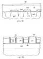
- FIG. 1illustrates a top view layout of a memory device 100 according to one embodiment of the present invention.
- This memory device 100is generally used for flash memory, but can be used for other types of memory as well.
- This viewillustrates wordlines 104 , digitlines 102 and a unit cell or memory cell 101 .
- the unit cell or memory cell 101is one of many cells of the memory device 100 .
- the memory cellhas a minimum feature size of 1F or F 105 in a first dimension which is half of the digitline pitch and a feature size of 2F 106 in a second dimension which is the wordline pitch.
- the square feature size or feature area of the cellis thus equal to 2F 2 .
- the memory cells of this memory device 100are formed using conventional silicon processing technology.
- a select transistor having a select gate 205 , source 201 and drain 203is formed as a part of the memory cell 101 .
- the select gate 205 and a floating gate 206are formed substantially perpendicular to each other.
- the select gate 205 of the select transistor and the floating gate 206make up the minimum feature size of the memory cell 101 .
- FIG. 2Aillustrates a cross section of the memory device 100 along the 2 A- 2 A line of FIG. 1.
- An n-type layer 201is formed over a substrate. This n-type layer 201 operates as a source.
- a p-type layer 202is formed over the n-type layer 201 .
- the p-type layer 202can be formed using epitaxial deposition or any other suitable fabrication scheme.
- One or more drains 203are formed in the p-type layer 202 .
- a vertical channel 212is thus created.
- a select gate 205is formed for each pair of memory cells of the memory device 100 .
- the select gate 205is formed vertically.
- Digitlines 102are formed over at least a portion of the drains 203 .
- the digitlines 102comprise a tungsten layer 210 and a spacer 213 formed over the tungsten layer 210 . Additionally, the digitlines 102 may comprise additional layers such as are described in FIG. 8A.
- One or more self aligned floating gates 206are formed horizontally as shown in FIG. 2A and are perpendicular to the select gates 205 .
- the self aligned floating gates 206can be fabricated any number of ways such as by forming a first oxide layer over a substrate, a poly layer over the first oxide and a second oxide layer over the poly layer.
- the self aligned floating gates 206are sub lithographic features and sub lithographic floating gates. Sub lithographic features are generally created using a removable spacer.
- FIGS. 8A, 8B, 8 C and 8 Dillustrate another example of fabricating the self aligned floating gates 206 .
- FIG. 2Billustrates a cross section of the memory device 100 across the 2 B- 2 B line of FIG. 1.
- One or more wordlines 104are formed over the spacers 213 .
- the spacer 213is formed of a material selected to insulate the wordlines 104 from the digitlines 102 .
- a shallow trench isolation (STI) area 211has been formed by etching a trench and depositing a trench oxide layer and filling the trench with oxide.
- a TiSi layer 221is formed on the STI area 211 and a TiN layer 220 is formed on the TiSi layer 221 below the tungsten layer 210 .
- STIshallow trench isolation
- FIG. 2Cillustrates a cross section of the memory device 100 across the 2 C- 2 C line of FIG. 1.
- the vertical select gates 205are shown.
- FIG. 2Dillustrates a cross section of the memory device 100 across the 2 D- 2 D line of FIG. 1.
- boron-doped phosphosilicate glass (BPSG) layer 214is formed over the STI area 211 .
- a hardmask 215is formed over the BPSG 214 .
- the memory device 100 shown in FIGS. 1, 2A, 2 B, 2 C and 2 Dconstitutes a 2F 2 memory cell. It is noted that in fabricating the device 100 , removable spacers 216 , see FIG. 2A, may be provided over the floating gates 206 to allow for sublithography to be possible. The removable spacers 216 are merely illustrated with broken lines because they have been removed. Only one removable spacer 216 is shown to preserve clarity. The placement of the select gate reduces over-erasure. Over-erasure is a condition that commonly occurs in flash memory cells in which Vt is caused to go below 0 which causes a transition and conducts or shorts a column of memory cells to ground. Additionally, programming efficiency is increased due to the floating gate 206 being directly above the vertical channel 212 .
- FIGS. 3A, 3B, 3 C and 3 Dillustrate a method of fabricating a memory device according to another embodiment of the present invention.
- An array maskis used to cover a periphery of a wafer at block 301 .
- Buried sources 502see FIG. 5, are implanted with a dopant at block 302 .
- the dopant usedcan be As or Sb.
- An annealis performed at block 303 .
- the waferis cleaned at block 304 .
- the wafercan be cleaned using any number of methods such as by using hydrofluoric acid (HF).
- An epitaxial deposition (EPI)is performed at block 305 to form a p-type channel 503 of a desired thickness, see FIG. 5.
- the desired thicknesssets the channel length.
- the EPIis performed with a dopant such as boron.
- FIG. 5illustrates a cross section of the memory device at this stage of processing.
- FIG. 5shows a p-type substrate 501 , buried sources 502 and a p-type channel 503 .
- FIG. 4is a top level view of a memory device fabricated by the method of FIGS. 3A, 3B, 3 C and 3 D.
- the viewshows a memory cell 405 , wordlines 404 and digitlines 402 .
- the viewalso shows cross sectional lines A-A, B-B, C-C and D-D which are described in further detail below.
- FIGS. 6 A- 8 Dillustrate cross sections of a memory device of the present invention at successive points in the fabrication scheme of the present invention.
- a cell implantis performed at block 306 .
- a tunnel oxide layer 604is formed over a substrate 608 at block 307 .
- a first poly layer 605is formed over the tunnel oxide layer 604 at block 308 .
- a nitride layer(not shown) is formed or deposited over the first poly layer 605 at block 309 .
- Areas for the wordlines 404are patterned into the memory device at block 310 .
- the nitride layer, first poly layer 605 and a trenchare etched at block 311 to form STI trenches or areas 607 .
- a shallow trench isolation (STI) oxide layer(not shown) is deposited at block 312 .
- STIshallow trench isolation
- the STI oxide layerrounds out the corners of the trench 607 .
- the STI trench 607is filled with oxide at block 313 .
- the surface of the memory deviceis polished or planarized using mechanical planarization at block 314 .
- An exemplary type of mechanical planarization which can be usedis a chemical mechanical planarization (CMP).
- CMPchemical mechanical planarization
- FIGS. 6A, 6B and 6 Cshow the memory device at this stage of the method and, more particularly, show the floating gate 610 and it's alignment to the STI areas 607 . This alignment makes the floating gate 610 a self aligning floating gate.
- FIG. 6Aillustrates a cross section of the memory device in the process of fabrication with reference to the A-A line of FIG. 4.
- the tunnel oxide layer 604is shown formed over the silicon substrate 608 .
- the first poly layer 605is formed over the tunnel oxide layer 604 .
- the ONO layer 606is formed over the first poly layer 605 .
- FIG. 6Billustrates a cross section of the memory device in the process of fabrication with reference to the B-B and C-C lines of FIG. 4. This shows how the ONO layer 606 has formed into horizontal and vertical portions.
- FIG. 6Cillustrates a cross section of the memory device in the process of fabrication with reference to the D-D line of FIG. 4 and shows the STI area 607 over the substrate 608 .
- a boron-doped phosphosilicate glass (BPSG) layer 717is deposited at block 318 over the ONO layer 606 .
- Rapid thermal processing (RTP)is performed on the memory device at block 319 .
- RTPsubjects the memory device to a short, controlled thermal cycle.
- the surface of the memory deviceis optionally polished by using mechanical planarization again and a hardmask layer 710 is deposited at block 320 .
- the digitlines or active area 402 of the memory deviceare patterned at block 321 .
- the digitlines or active area 402are etched at block 322 down to the tunnel oxide layer 604 to form a trench or active trench 718 .
- the hardmask layer 710 , BPSG layer 717 , ONO layer 606 and first poly layer 605 of the trench 718are etched away, but the tunnel oxide layer 604 is not etched.
- a first spacer layeris deposited and etched at block 323 to vertically form first spacers 711 . Drains 714 are formed in the active areas or columns by implanting a dopant at block 324 . Another RTP is performed at block 325 .
- TiSi 713 and TiN 712 layersare formed over the drains 714 at block 326 .
- the TiN 712 and TiSi 713 layersare formed horizontally and vertically in the active trench 718 .
- Another RTPis performed at block 327 .
- a tungsten layer 716is deposited over the active areas or columns in the active trench 718 at block 328 .
- Mechanical planarizationis performed on the memory device so that the tungsten layer 716 is planar with the hardmask at block 329 .
- the tungsten layer 716is etched such that approximately half is removed at block 330 .
- Second spacers 715are deposited over the tungsten layer 716 at block 331 .
- the second spacers 715fill the rest of the trench so the height of the active area or columns is approximately equal to the height of the hard mask 710 .
- the digitlines 402comprise the second spacers 715 and the tungsten layer 716 .
- the digitlines 402are insulated because of the second spacers 715 .
- FIGS. 7A, 7B, 7 C and 7 Dillustrate the formation of digitlines 402 .
- FIG. 7Ashows a cross section of the memory device in the process of fabrication with reference to the A-A line of FIG. 4.
- the BPSG layer 717is formed over the ONO layer 606 .
- the hardmask 710is formed over the BPSG layer 717 .
- the first spacers 711are formed vertically adjacent to the BPSG layers after the trench 718 has been etched away.
- FIG. 7Bshows a cross section of the memory device in the process of fabrication with reference to the B-B line of FIG. 4.
- FIG. 7Cshows a cross section of the memory device in the process of fabrication with reference to the C-C line of FIG. 4.
- FIG. 7Dshows a cross section of the memory device in the process of fabrication with reference to the D-D line of FIG. 4.
- the hardmask layer 710 and BPSG layer 717are removed or etched from the wordlines 404 at block 332 .
- a removable spacer 825is deposited at block 333 . Only one removable spacer is shown in the figures to preserve clarity.
- the removable spacer 825is etched at block 334 .
- At least one select trench 820is formed by etching the ONO layer 606 , first poly layer 605 , the tunnel oxide 604 and silicon to a desired depth at block 335 . The remaining portion of the removable spacer 825 is removed at block 336 .
- a select transistor oxide layer 822is formed on the surface of the select trench 820 .
- a second poly layer 821is formed over the surface of the memory device, including the select trench 820 and a WSi x layer 823 is deposited over the second poly layer 821 at block 338 .
- the second poly layer 821is also referred to as the wordline poly.
- the second poly layer 821 and WSi x layer 823are patterned at block 339 and etched at block 340 . By etching and removing the removable spacer 825 , the second poly layer 821 and floating gate 605 are capacitively coupled.
- FIGS. 8A, 8B, 8 C and 8 Dshow wordline 404 formation.
- FIG. 8Ais a cross section of the memory device in the process of fabrication with reference to the A-A line of FIG. 4.
- the select trenches 820have a layer of select gate oxide 822 and are filled with the second poly layer 821 .
- the removable spacer 825has been removed.
- the second poly layer 821is shown in the select trenches 820 and other areas.
- FIG. 8Bis a cross section of the memory device in the process of fabrication with reference to the B-B line of FIG. 4.
- the wordlines 404are shown and comprise the WSi X layer 823 formed over the second poly layer 821 formed over the second spacer 715 .
- the rowlines 404are insulated from the tungsten layer 716 by the second spacer 715 .
- FIG. 8Cillustrates a cross section of the memory device in the process of fabrication with reference to the C-C line of FIG. 4.
- the select trenches 820are shown.
- FIG. 8Dillustrates a cross section of the memory device in the process of fabrication with reference to the D-D line of FIG. 4.
- FIG. 9is an illustration of a computer system 912 that can use and be used with embodiments of the present invention.
- the computer systemcan be a desktop, network server, handheld computer or the like.
- the computer system 912would include ROM 914 , mass memory 916 , peripheral devices 918 , and I/O devices 920 in communication with a microprocessor 922 via a data bus 924 or another suitable data communication path.
- the memory devices 914 and 916can be fabricated according to the various embodiments of the present invention, including memory devices having a square feature size of 2F 2 .
- ROM 914can include EPROM or EEPROM or flash memory.
- Mass memory 916can include DRAM, synchronous RAM or flash memory.
- the present inventorrecognizes that other 3-dimensional memory cells place the floating gate in the sidewall of a trench in the ⁇ 111> plane or other planes which have a higher density of bonds. This placement typically results in an inferior oxide resulting in retention, cycling and trapping problems with the memory cell.
- the present inventiongenerally places the floating gate in the ⁇ 100> plane thereby avoiding the aforementioned results.
- a “flash memory device”includes a plurality of memory cells. Each “memory cell” of a flash memory device can comprise components such as a gate, floating gate, control gate, wordline, channel region, a source, self aligned source and a drain.
- patterningrefers to one or more steps that result in the removal of selected portions of layers. The patterning process is also known by the names photomasking, masking, photolithography and microlithography.
- the term “self-aligned gate”refers to a memory device where the gate electrodes are formed before the source/drain diffusions are made.
- An “anneal”is a high temperature processing step designed to minimize stress in the crystal structure of the wafer.
- An “epitaxial deposition” (EPI)involves depositing a layer of high-quality, single-crystal silicon on a wafer surface to form a base.
- the term “rapid thermal processing (RTP)”refers to a process that subjects a wafer to a short, yet controlled, thermal cycle which heats the wafer from room temperature to a high temperature, such as 1200° C., in a few seconds.
- memory devicescan be used in electronic devices such as cell phones, digital cameras, digital video cameras, digital audio players, cable television set top boxes, digital satellite receivers, personal digital assistants and the like.
- large capacity flash memory chipscan be fabricated. For example, a 0.45 ⁇ 2 cell can be realized in 0.15 ⁇ technology using a 2F 2 memory cell.
- the substratemay be composed of semiconductors such as gallium arsenide or germanium.
- other dopantsmay be utilized besides those specifically stated. Generally, dopants are found in groups III and V of the periodic table.
Landscapes
- Non-Volatile Memory (AREA)
- Semiconductor Memories (AREA)
- Static Random-Access Memory (AREA)
Abstract
Description
- The present invention relates to the field of semiconductor manufacture and, more particularly, to a 2F[0001]2flash memory.
- As computers become increasingly complex, the need for improved memory storage increases. At the same time, there is a continuing drive to reduce the size of computers and memory devices. Accordingly, a goal of memory device fabrication is to increase the number of memory cells per unit area.[0002]
- Memory devices contain blocks or arrays of memory cells. A memory cell stores one bit of information. Bits are commonly represented by the[0003]
binary digits 0 and 1. A flash memory device is a non-volatile semiconductor memory device in which contents in a single cell or a block of memory cells are electrically programmable and may be read or written in a single operation. Flash memory devices have the characteristics of low power and fast operation making them ideal for portable devices. Flash memory is commonly used in portable devices such as laptop or notebook computers, digital audio players and personal digital assistant (PDA) devices. - In flash memory, a charged floating gate is one logic state, typically represented by the[0004]
binary digit 1, while a non-charged floating gate is the opposite logic state typically represented by the binary digit 0. Charges are injected or written to a floating gate by any number of methods, including avalanche injection, channel injection, Fowler-Nordheim tunneling, and channel hot electron injection, for example. - A memory cell or flash memory cell may be characterized in terms of its minimum feature size (F) and cell area (F[0005]2). For
- example, a standard NOR flash cell is typically quoted as a ten square feature cell and a standard NAND flash cell is approximately a 4.5 square feature cell. Typical DRAM (dynamic random access memory) cells are between 8 F[0006]2and 6 F2. Cell area (F2) is determined according to a well known methodology and represents the multiple of the number of features along the x and y dimensions of a memory cell. A suitable illustration of feature size is presented in U.S. Pat. No. 6,043,562, the disclosure of which is incorporated herein by reference.
- Memory devices can be created using 2-dimensional structures or using 3-dimensional structures. The 2-dimensional structures are also referred to as planar structures. Generally, 3-dimensional structures yield smaller cell sizes than planar structures. SRAMs and DRAMs have been designed using 3-dimensional structures, however few flash memory cells are fabricated using 3-dimensional structures. Most flash memory cells are fabricated using planar structures. Some flash memory cells have been fabricated using 3-dimensional structures, but they are, generally, in the size range of 4.5 F[0007]2to 8 F2which are not significantly smaller than flash memory cells fabricated using planar structures.
- Accordingly, there is a need for a 3-dimensional flash memory device having a cell area of reduced square feature size.[0008]
- According to one embodiment of the invention, a memory cell is disclosed. The memory cell comprises a source, a vertical channel, a drain and a horizontal floating gate. The vertical channel is formed over the source. The drain is formed over the vertical channel. The horizontal floating gate is formed over at least a portion of the drain.[0009]
- According to another embodiment of the invention, a memory cell is disclosed. The memory cell comprises a source, a vertical channel, a drain, a horizontal floating gate and a vertical select gate. The vertical channel is formed over the source. The drain is formed over the vertical channel. The horizontal floating gate is formed over at least a portion of the drain. The vertical select gate is formed perpendicular to the horizontal floating gate.[0010]
- According to yet another embodiment of the invention, a memory cell is disclosed. The memory cell comprises a first transistor and a select transistor. The first transistor comprises a source, a drain and a gate. The select transistor is coupled to the first transistor and comprises a source, a drain and a gate. The gate of the select transistor is formed perpendicular to the gate of the first transistor.[0011]
- According to yet another embodiment of the present invention, a memory device is disclosed. The memory device includes a first n-type layer, a p-type layer and a second n-type layer. The p-type layer is formed over the first n-type layer. The second n-type layer is formed over the p-type layer forming a vertical channel.[0012]
- According to yet another embodiment of the invention, a memory device is disclosed. The memory device includes a horizontal first n-type layer, a p-type layer, a horizontal second n-type layer, a horizontal floating gate and a vertical select gate. The horizontal first n-type layer is formed over a substrate. The p-type layer is formed over the first n-type layer. The horizontal second n-type layer is formed over the p-type layer. The horizontal floating gate is formed over the substrate. The vertical select gate is formed over the substrate. The p-type layer formed a vertical channel. The first n-type layer forms a buried source and the second n-type layer forms a drain.[0013]
- According to yet another embodiment of the invention, a memory device is disclosed. The memory device includes a buried source, a vertical channel, a drain, a floating gate and a select gate. The buried source is formed over a substrate. The vertical channel is formed over the buried source. The drain is formed over the vertical channel. The floating gate is formed over the substrate. The select gate is formed perpendicular to the floating gate in a trench formed in the substrate. The memory device has a square feature size of 2F[0014]2.
- According to yet another embodiment of the invention, a memory device is disclosed. The memory device includes a substrate, a first n-type layer, a p-type layer, a second n-type layer, a floating gate, a trench and a select gate. The substrate has at least one semiconductor layer. The first n-type layer is formed over the substrate. The p-type layer is formed over the first n-type layer. The second n-type layer is formed over the p-type layer. The floating gate is formed over the substrate. The trench is formed in the substrate. The select gate is formed on a sidewall of the trench.[0015]
- According to yet another embodiment of the invention, a memory device is disclosed. The memory device includes a first n-type layer, a p-type layer, a second n-type layer, a select trench, a vertical select gate, digitlines, a self aligned floating gate and wordlines. The p-type layer is formed over the n-type layer. The second n-type layer is formed in the p-type layer. The select trench is formed in the substrate. The vertical select gate is formed in the select trench. The digitlines are formed over the second n-type layer. The self aligned floating gate is formed over the n-type layer. The wordlines are formed over the substrate and the digitlines.[0016]
- According to yet another embodiment of the invention, a memory device is disclosed. The memory device includes a first n-type layer, a p-type layer, a second n-type layer, a select trench, a tungsten layer, a spacer, a tunnel oxide layer, a polysilicon layer and an oxide layer. The first n-type layer is formed over a substrate. The p-type layer is formed over the n-type layer. The second n-type layer is formed over the p-type layer. The select trench is formed in the substrate. The vertical select gate is formed in the select trench. The tungsten layer is formed over at least a portion of the second n-type layer. The spacer is formed over the tungsten layer. The tunnel oxide layer is formed over at least a portion of the substrate. The polysilicon layer is formed on the tunnel oxide layer. The oxide layer is formed on the polysilicon layer.[0017]
- According to yet another embodiment of the invention, a method of fabricating a memory device having a square feature size of 2F[0018]2is disclosed. A substrate is provided. A first n-type layer is formed over the substrate. A p-type layer is formed over the first n-type layer. A second n-type layer is formed over the p-type layer. A floating gate is formed over the substrate. A trench is formed in the memory device. A select gate is formed in the trench.
- According to yet another embodiment of the invention, a method of fabricating a buried source is disclosed. A wafer is provided having a substrate. A periphery of a wafer is covered using an array mask. Source areas are doped with a dopant. An epitaxial deposition is performed to form a p-type channel.[0019]
- According to another embodiment of the invention, a method of fabricating a memory device is disclosed. A wafer is provided having a substrate. A buried source is formed over the substrate. A vertical channel is formed over the buried source. A cell implant is performed. A tunnel oxide layer is formed over the substrate. A first poly layer is formed over the tunnel oxide layer. A nitride layer is formed over the first poly layer. Wordlines are patterned into the memory device. STI areas are formed in the memory device. The nitride layer is removed. An oxide nitride oxide layer is formed over a surface of the memory device.[0020]
- According to yet another embodiment of the invention, a method of fabricating a memory device is disclosed. A wafer is provided having a substrate. A buried source is formed over the substrate. A vertical channel is formed over the buried source. A STI area and a self aligned floating gate is formed. A BPSG layer is deposited over the substrate. A hardmask layer is deposited over the BPSG layer. Active areas are patterned to form an active trench. First spacers are formed along sidewalls of the active trench. A drain is formed in the active trench. A wordline is formed over the drain.[0021]
- According to another embodiment of the invention, a method of fabricating a memory device is disclosed. A buried source is formed in a substrate. A vertical channel is formed over the buried source. A STI area is formed in the memory device. A self aligned floating gate is formed over the substrate. Wordlines are formed over the substrate. A spacer is formed over the wordlines. Rowlines are formed over the substrate. A select gate is formed in a select trench in the substrate.[0022]
- The methods and devices disclosed, along with variations of them, provide for memory devices having square feature sizes as small as 2F[0023]2. Such square feature sizes can permit large memory devices, on the order of a gigabyte or larger, to be fabricated on one chip or die. The methods and devices disclosed, along with variations of them, represent a three dimensional fabrication scheme.
- The following detailed description of the present invention can be best understood when read in conjunction with the accompanying drawings, where like structure is indicated with like reference numerals.[0024]
- FIG. 1 illustrates a top view layout of a memory device according to one embodiment of the present invention;[0025]
- FIG. 2A illustrates a cross section of a memory device according to one embodiment of the present invention with reference to[0026]
line 2A-2A of FIG. 1; - FIG. 2B illustrates a cross section of a memory device according to one embodiment of the present invention with reference to[0027]
line 2B-2B of FIG. 1; - FIG. 2C illustrates a cross section of a memory device according to one embodiment of the present invention with reference to line[0028]2C-2C of FIG. 1;
- FIG. 2D illustrates a cross section of a memory device according to one embodiment of the present invention with reference to[0029]
line 2D-2D of FIG. 1; - FIGS.[0030]3A-3D illustrates a method of fabricating a memory device according to another embodiment of the present invention;
- FIG. 4 illustrates a top view of a memory device fabricated according to the method of FIG. 3;[0031]
- FIG. 5 illustrates a portion of a memory device at a selected stage of processing according to the method of FIG. 3;[0032]
- FIG. 6A illustrates a cross section of a memory device at a selected stage of processing according to the method of FIG. 3 with reference to line A-A of FIG. 4;[0033]
- FIG. 6B illustrates a cross section of a memory device at a selected stage of processing according to the method of FIG. 3 with reference to line B-B of FIG. 4;[0034]
- FIG. 6C illustrates a cross section of a memory device at a selected stage of processing according to the method of FIG. 3 with reference to line D-D of FIG. 4;[0035]
- FIG. 7A illustrates a cross section of a memory device at a selected stage of processing according to the method of FIG. 3 with reference to line A-A of FIG. 4;[0036]
- FIG. 7B illustrates a cross section of a memory device at a selected stage of processing according to the method of FIG. 3 with reference to line B-B of FIG. 4;[0037]
- FIG. 7C illustrates a cross section of a memory device at a selected stage of processing according to the method of FIG. 3 with reference to line C-C of FIG. 4;[0038]
- FIG. 7D illustrates a cross section of a memory device at a selected stage of processing according to the method of FIG. 3 with reference to line D-D of FIG. 4;[0039]
- FIG. 8A illustrates a cross section of a memory device at a selected stage of processing according to the method of FIG. 3 with reference to line A-A of FIG. 4;[0040]
- FIG. 8B illustrates a cross section of a memory device at a selected stage of processing according to the method of FIG. 3 with reference to line B-B of FIG. 4;[0041]
- FIG. 8C illustrates a cross section of a memory device at a selected stage of processing according to the method of FIG. 3 with reference to line C-C of FIG. 4;[0042]
- FIG. 8D illustrates a cross section of a memory device at a selected stage of processing according to the method of FIG. 3 with reference to line D-D of FIG. 4; and[0043]
- FIG. 9 illustrates a computer system in which embodiments of the present invention may be used.[0044]
- FIG. 1 illustrates a top view layout of a[0045]
memory device 100 according to one embodiment of the present invention. Thismemory device 100 is generally used for flash memory, but can be used for other types of memory as well. This view illustrateswordlines 104,digitlines 102 and a unit cell or memory cell101. The unit cell or memory cell101 is one of many cells of thememory device 100. The memory cell has a minimum feature size of 1F orF 105 in a first dimension which is half of the digitline pitch and a feature size of2F 106 in a second dimension which is the wordline pitch. The square feature size or feature area of the cell is thus equal to 2F2. The memory cells of thismemory device 100 are formed using conventional silicon processing technology. As is described in further detail herein with reference to FIGS. 2A, 2B,2C and2D, a select transistor having aselect gate 205,source 201 and drain203 is formed as a part of the memory cell101. Theselect gate 205 and a floatinggate 206 are formed substantially perpendicular to each other. Theselect gate 205 of the select transistor and the floatinggate 206 make up the minimum feature size of the memory cell101. - FIG. 2A illustrates a cross section of the[0046]
memory device 100 along the2A-2A line of FIG. 1. An n-type layer 201 is formed over a substrate. This n-type layer 201 operates as a source. A p-type layer 202 is formed over the n-type layer 201. The p-type layer 202 can be formed using epitaxial deposition or any other suitable fabrication scheme. One ormore drains 203 are formed in the p-type layer 202. Avertical channel 212 is thus created. Aselect gate 205 is formed for each pair of memory cells of thememory device 100. Theselect gate 205 is formed vertically. - [0047]
Digitlines 102 are formed over at least a portion of thedrains 203. Thedigitlines 102 comprise atungsten layer 210 and aspacer 213 formed over thetungsten layer 210. Additionally, thedigitlines 102 may comprise additional layers such as are described in FIG. 8A. One or more self aligned floatinggates 206 are formed horizontally as shown in FIG. 2A and are perpendicular to theselect gates 205. The self aligned floatinggates 206 can be fabricated any number of ways such as by forming a first oxide layer over a substrate, a poly layer over the first oxide and a second oxide layer over the poly layer. The self aligned floatinggates 206 are sub lithographic features and sub lithographic floating gates. Sub lithographic features are generally created using a removable spacer. FIGS. 8A, 8B,8C and8D illustrate another example of fabricating the self aligned floatinggates 206. - FIG. 2B illustrates a cross section of the[0048]
memory device 100 across the2B-2B line of FIG. 1. One or more wordlines104, each comprising asecond poly layer 209 and aWSiX layer 208, are formed over thespacers 213. Thespacer 213 is formed of a material selected to insulate thewordlines 104 from thedigitlines 102. A shallow trench isolation (STI)area 211 has been formed by etching a trench and depositing a trench oxide layer and filling the trench with oxide. ATiSi layer 221 is formed on theSTI area 211 and aTiN layer 220 is formed on theTiSi layer 221 below thetungsten layer 210. - FIG. 2C illustrates a cross section of the[0049]
memory device 100 across the2C-2C line of FIG. 1. The verticalselect gates 205 are shown. FIG. 2D illustrates a cross section of thememory device 100 across the2D-2D line of FIG. 1. A - boron-doped phosphosilicate glass (BPSG)[0050]
layer 214 is formed over theSTI area 211. Ahardmask 215 is formed over theBPSG 214. - The[0051]
memory device 100 shown in FIGS. 1, 2A,2B,2C and2D constitutes a 2F2memory cell. It is noted that in fabricating thedevice 100,removable spacers 216, see FIG. 2A, may be provided over the floatinggates 206 to allow for sublithography to be possible. Theremovable spacers 216 are merely illustrated with broken lines because they have been removed. Only oneremovable spacer 216 is shown to preserve clarity. The placement of the select gate reduces over-erasure. Over-erasure is a condition that commonly occurs in flash memory cells in which Vt is caused to go below 0 which causes a transition and conducts or shorts a column of memory cells to ground. Additionally, programming efficiency is increased due to the floatinggate 206 being directly above thevertical channel 212. - FIGS. 3A, 3B,[0052]3C and3D illustrate a method of fabricating a memory device according to another embodiment of the present invention. An array mask is used to cover a periphery of a wafer at
block 301. Buriedsources 502, see FIG. 5, are implanted with a dopant atblock 302. The dopant used can be As or Sb. An anneal is performed atblock 303. The wafer is cleaned atblock 304. The wafer can be cleaned using any number of methods such as by using hydrofluoric acid (HF). An epitaxial deposition (EPI) is performed atblock 305 to form a p-type channel 503 of a desired thickness, see FIG. 5. The desired thickness sets the channel length. The EPI is performed with a dopant such as boron. - FIG. 5 illustrates a cross section of the memory device at this stage of processing. FIG. 5 shows a p-[0053]
type substrate 501, buriedsources 502 and a p-type channel 503. - FIG. 4 is a top level view of a memory device fabricated by the method of FIGS. 3A, 3B,[0054]3C and3D. The view shows a memory cell405,
wordlines 404 anddigitlines 402. The view also shows cross sectional lines A-A, B-B, C-C and D-D which are described in further detail below. FIGS.6A-8D illustrate cross sections of a memory device of the present invention at successive points in the fabrication scheme of the present invention. - Referring to FIGS. 6A, 6B,[0055]6C and3B, a cell implant is performed at
block 306. Atunnel oxide layer 604 is formed over asubstrate 608 atblock 307. Afirst poly layer 605 is formed over thetunnel oxide layer 604 atblock 308. A nitride layer (not shown) is formed or deposited over thefirst poly layer 605 atblock 309. Areas for thewordlines 404 are patterned into the memory device atblock 310. The nitride layer,first poly layer 605 and a trench are etched atblock 311 to form STI trenches orareas 607. A shallow trench isolation (STI) oxide layer (not shown) is deposited atblock 312. The STI oxide layer rounds out the corners of thetrench 607. TheSTI trench 607 is filled with oxide atblock 313. The surface of the memory device is polished or planarized using mechanical planarization atblock 314. An exemplary type of mechanical planarization which can be used is a chemical mechanical planarization (CMP). The polishing makes the surface of the memory device planar. - The nitride layer is removed at[0056]
block 315. An oxide nitride oxide (ONO)layer 606 is formed over the surface of the memory device atblock 316. FIGS. 6A, 6B and6C show the memory device at this stage of the method and, more particularly, show the floatinggate 610 and it's alignment to theSTI areas 607. This alignment makes the floating gate610 a self aligning floating gate. - FIG. 6A illustrates a cross section of the memory device in the process of fabrication with reference to the A-A line of FIG. 4. The[0057]
tunnel oxide layer 604 is shown formed over thesilicon substrate 608. Thefirst poly layer 605 is formed over thetunnel oxide layer 604. TheONO layer 606 is formed over thefirst poly layer 605. FIG. 6B illustrates a cross section of the memory device in the process of fabrication with reference to the B-B and C-C lines of FIG. 4. This shows how theONO layer 606 has formed into horizontal and vertical portions. FIG. 6C illustrates a cross section of the memory device in the process of fabrication with reference to the D-D line of FIG. 4 and shows theSTI area 607 over thesubstrate 608. - Referring to FIGS. 3C, 7A,[0058]7B,7C and7D, a boron-doped phosphosilicate glass (BPSG)
layer 717 is deposited atblock 318 over theONO layer 606. Rapid thermal processing (RTP) is performed on the memory device atblock 319. RTP subjects the memory device to a short, controlled thermal cycle. The surface of the memory device is optionally polished by using mechanical planarization again and ahardmask layer 710 is deposited atblock 320. - The digitlines or[0059]
active area 402 of the memory device are patterned atblock 321. The digitlines oractive area 402 are etched atblock 322 down to thetunnel oxide layer 604 to form a trench oractive trench 718. Thehardmask layer 710,BPSG layer 717,ONO layer 606 andfirst poly layer 605 of thetrench 718 are etched away, but thetunnel oxide layer 604 is not etched. A first spacer layer is deposited and etched atblock 323 to vertically formfirst spacers 711.Drains 714 are formed in the active areas or columns by implanting a dopant atblock 324. Another RTP is performed atblock 325.TiSi 713 andTiN 712 layers are formed over thedrains 714 atblock 326. TheTiN 712 andTiSi 713 layers are formed horizontally and vertically in theactive trench 718. Another RTP is performed atblock 327. Atungsten layer 716 is deposited over the active areas or columns in theactive trench 718 atblock 328. Mechanical planarization is performed on the memory device so that thetungsten layer 716 is planar with the hardmask atblock 329. Thetungsten layer 716 is etched such that approximately half is removed atblock 330.Second spacers 715 are deposited over thetungsten layer 716 atblock 331. Thesecond spacers 715 fill the rest of the trench so the height of the active area or columns is approximately equal to the height of thehard mask 710. - The[0060]
digitlines 402 comprise thesecond spacers 715 and thetungsten layer 716. Thedigitlines 402 are insulated because of thesecond spacers 715. FIGS. 7A, 7B,7C and7D illustrate the formation ofdigitlines 402. FIG. 7A shows a cross section of the memory device in the process of fabrication with reference to the A-A line of FIG. 4. TheBPSG layer 717 is formed over theONO layer 606. Thehardmask 710 is formed over theBPSG layer 717. Thefirst spacers 711 are formed vertically adjacent to the BPSG layers after thetrench 718 has been etched away. Thetungsten layer 716 is formed over the Ti layers,TiN 712 andTiSi 713. Thesecond spacers 715 are formed over thetungsten layer 716 in the trench oractive areas 718. FIG. 7B shows a cross section of the memory device in the process of fabrication with reference to the B-B line of FIG. 4. FIG. 7C shows a cross section of the memory device in the process of fabrication with reference to the C-C line of FIG. 4. FIG. 7D shows a cross section of the memory device in the process of fabrication with reference to the D-D line of FIG. 4. - Referring to FIGS. 3D, 8A,[0061]8B,8C and8D, the
hardmask layer 710 andBPSG layer 717 are removed or etched from thewordlines 404 atblock 332. Aremovable spacer 825 is deposited atblock 333. Only one removable spacer is shown in the figures to preserve clarity. Theremovable spacer 825 is etched atblock 334. At least oneselect trench 820 is formed by etching theONO layer 606,first poly layer 605, thetunnel oxide 604 and silicon to a desired depth atblock 335. The remaining portion of theremovable spacer 825 is removed atblock 336. A selecttransistor oxide layer 822 is formed on the surface of theselect trench 820. Asecond poly layer 821 is formed over the surface of the memory device, including theselect trench 820 and a WSixlayer823 is deposited over thesecond poly layer 821 atblock 338. Thesecond poly layer 821 is also referred to as the wordline poly. Thesecond poly layer 821 and WSixlayer823 are patterned atblock 339 and etched atblock 340. By etching and removing theremovable spacer 825, thesecond poly layer 821 and floatinggate 605 are capacitively coupled. FIGS. 8A, 8B,8C and8D show wordline404 formation. FIG. 8A is a cross section of the memory device in the process of fabrication with reference to the A-A line of FIG. 4. Theselect trenches 820 have a layer ofselect gate oxide 822 and are filled with thesecond poly layer 821. Theremovable spacer 825 has been removed. Thesecond poly layer 821 is shown in theselect trenches 820 and other areas. FIG. 8B is a cross section of the memory device in the process of fabrication with reference to the B-B line of FIG. 4. Thewordlines 404 are shown and comprise the WSiXlayer823 formed over thesecond poly layer 821 formed over thesecond spacer 715. Thus, therowlines 404 are insulated from thetungsten layer 716 by thesecond spacer 715. FIG. 8C illustrates a cross section of the memory device in the process of fabrication with reference to the C-C line of FIG. 4. Theselect trenches 820 are shown. FIG. 8D illustrates a cross section of the memory device in the process of fabrication with reference to the D-D line of FIG. 4. - FIG. 9 is an illustration of a computer system[0062]912 that can use and be used with embodiments of the present invention. The computer system can be a desktop, network server, handheld computer or the like. As will be appreciated by those skilled in the art, the computer system912 would include
ROM 914,mass memory 916,peripheral devices 918, and I/O devices 920 in communication with amicroprocessor 922 via adata bus 924 or another suitable data communication path. Thememory devices ROM 914 can include EPROM or EEPROM or flash memory.Mass memory 916 can include DRAM, synchronous RAM or flash memory. - The present inventor recognizes that other 3-dimensional memory cells place the floating gate in the sidewall of a trench in the <111> plane or other planes which have a higher density of bonds. This placement typically results in an inferior oxide resulting in retention, cycling and trapping problems with the memory cell. The present invention generally places the floating gate in the <100> plane thereby avoiding the aforementioned results.[0063]
- For the purposes of describing and defining the present invention, formation of a material “on” a substrate or layer refers to formation in contact with a surface of the substrate or layer. Formation “over” a substrate or layer refers to formation above or in contact with a surface of the substrate. A “flash memory device” includes a plurality of memory cells. Each “memory cell” of a flash memory device can comprise components such as a gate, floating gate, control gate, wordline, channel region, a source, self aligned source and a drain. The term “patterning” refers to one or more steps that result in the removal of selected portions of layers. The patterning process is also known by the names photomasking, masking, photolithography and microlithography. The term “self-aligned gate” refers to a memory device where the gate electrodes are formed before the source/drain diffusions are made. An “anneal” is a high temperature processing step designed to minimize stress in the crystal structure of the wafer. An “epitaxial deposition” (EPI) involves depositing a layer of high-quality, single-crystal silicon on a wafer surface to form a base. The term “rapid thermal processing (RTP)” refers to a process that subjects a wafer to a short, yet controlled, thermal cycle which heats the wafer from room temperature to a high temperature, such as 1200° C., in a few seconds.[0064]
- Many other electronic devices can be fabricated utilizing various embodiments of the present invention. For example, memory devices according to embodiments of the invention can be used in electronic devices such as cell phones, digital cameras, digital video cameras, digital audio players, cable television set top boxes, digital satellite receivers, personal digital assistants and the like. Additionally, large capacity flash memory chips can be fabricated. For example, a 0.45μ[0065]2cell can be realized in 0.15μ technology using a 2F2memory cell.
- Having described the invention in detail and by reference to preferred embodiments thereof, it will be apparent that modifications and variations are possible without departing from the scope of the present invention defined in the appended claims. Other suitable materials may be substituted for those specifically recited herein. For example, the substrate may be composed of semiconductors such as gallium arsenide or germanium. Additionally, other dopants may be utilized besides those specifically stated. Generally, dopants are found in groups III and V of the periodic table.[0066]
Claims (68)
Priority Applications (7)
| Application Number | Priority Date | Filing Date | Title |
|---|---|---|---|
| US09/802,234US6759707B2 (en) | 2001-03-08 | 2001-03-08 | 2F2 memory device system |
| KR1020037011822AKR100659164B1 (en) | 2001-03-08 | 2002-02-27 | 2F2 memory device system and method |
| CNB028087763ACN100341153C (en) | 2001-03-08 | 2002-02-27 | 2f2 memory device system and method |
| PCT/US2002/005716WO2002073698A2 (en) | 2001-03-08 | 2002-02-27 | A 2f2 memory device system and method |
| EP02750562AEP1366525A2 (en) | 2001-03-08 | 2002-02-27 | A 2f?2 memory device system and method |
| JP2002572643AJP2005500670A (en) | 2001-03-08 | 2002-02-27 | 2F2 memory device system and method |
| US10/755,990US6998314B2 (en) | 2001-03-08 | 2004-01-13 | Fabricating a 2F2 memory device with a horizontal floating gate |
Applications Claiming Priority (1)
| Application Number | Priority Date | Filing Date | Title |
|---|---|---|---|
| US09/802,234US6759707B2 (en) | 2001-03-08 | 2001-03-08 | 2F2 memory device system |
Related Child Applications (1)
| Application Number | Title | Priority Date | Filing Date |
|---|---|---|---|
| US10/755,990DivisionUS6998314B2 (en) | 2001-03-08 | 2004-01-13 | Fabricating a 2F2 memory device with a horizontal floating gate |
Publications (2)
| Publication Number | Publication Date |
|---|---|
| US20020127798A1true US20020127798A1 (en) | 2002-09-12 |
| US6759707B2 US6759707B2 (en) | 2004-07-06 |
Family
ID=25183165
Family Applications (2)
| Application Number | Title | Priority Date | Filing Date |
|---|---|---|---|
| US09/802,234Expired - LifetimeUS6759707B2 (en) | 2001-03-08 | 2001-03-08 | 2F2 memory device system |
| US10/755,990Expired - Fee RelatedUS6998314B2 (en) | 2001-03-08 | 2004-01-13 | Fabricating a 2F2 memory device with a horizontal floating gate |
Family Applications After (1)
| Application Number | Title | Priority Date | Filing Date |
|---|---|---|---|
| US10/755,990Expired - Fee RelatedUS6998314B2 (en) | 2001-03-08 | 2004-01-13 | Fabricating a 2F2 memory device with a horizontal floating gate |
Country Status (6)
| Country | Link |
|---|---|
| US (2) | US6759707B2 (en) |
| EP (1) | EP1366525A2 (en) |
| JP (1) | JP2005500670A (en) |
| KR (1) | KR100659164B1 (en) |
| CN (1) | CN100341153C (en) |
| WO (1) | WO2002073698A2 (en) |
Cited By (16)
| Publication number | Priority date | Publication date | Assignee | Title |
|---|---|---|---|---|
| US20030227048A1 (en)* | 2002-04-01 | 2003-12-11 | Sohrab Kianian | Self aligned method of forming a semiconductor memory array of floating gate memory cells with buried bit-line and raised source line, and a memory array made thereby |
| US20040202021A1 (en)* | 2001-07-02 | 2004-10-14 | Massimo Atti | Charge coupled eeprom device and corresponding method of operation |
| US20050247983A1 (en)* | 2004-05-05 | 2005-11-10 | Ting Steve M | Method of forming a raised source/drain and a semiconductor device employing the same |
| US20050269624A1 (en)* | 2002-04-05 | 2005-12-08 | Hu Yaw W | Self-aligned method of forming a semiconductor memory array of floating gate memory cells with buried source line and floating gate |
| US20070048942A1 (en)* | 2005-08-30 | 2007-03-01 | Micron Technology, Inc. | Methods of forming field effect transistors on substrates |
| US20070161205A1 (en)* | 2006-01-12 | 2007-07-12 | Shian-Jyh Lin | Electrical device and method for fabricating the same |
| US20080017918A1 (en)* | 2006-07-24 | 2008-01-24 | Seong-Gyun Kim | Three-dimensional flash memory cell |
| US7825462B2 (en) | 2004-09-01 | 2010-11-02 | Micron Technology, Inc. | Transistors |
| US7902028B2 (en) | 2006-02-02 | 2011-03-08 | Micron Technology, Inc. | Methods of forming field effect transistors, methods of forming field effect transistor gates, methods of forming integrated circuitry comprising a transistor gate array and circuitry peripheral to the gate array, and methods of forming integrated circuitry comprising a transistor gate array including first gates and second grounded isolation gates |
| US7944743B2 (en) | 2006-09-07 | 2011-05-17 | Micron Technology, Inc. | Methods of making a semiconductor memory device |
| US8067286B2 (en) | 2005-03-25 | 2011-11-29 | Micron Technology, Inc. | Methods of forming recessed access devices associated with semiconductor constructions |
| US8399920B2 (en)* | 2005-07-08 | 2013-03-19 | Werner Juengling | Semiconductor device comprising a transistor gate having multiple vertically oriented sidewalls |
| US8551823B2 (en) | 2006-07-17 | 2013-10-08 | Micron Technology, Inc. | Methods of forming lines of capacitorless one transistor DRAM cells, methods of patterning substrates, and methods of forming two conductive lines |
| US20150255614A1 (en)* | 2014-03-05 | 2015-09-10 | Powerchip Technology Corporation | Split gate flash memory and manufacturing method thereof |
| US10515801B2 (en) | 2007-06-04 | 2019-12-24 | Micron Technology, Inc. | Pitch multiplication using self-assembling materials |
| US20240304681A1 (en)* | 2023-03-10 | 2024-09-12 | Winbond Electronics Corp. | Semiconductor device and method of forming the same |
Families Citing this family (20)
| Publication number | Priority date | Publication date | Assignee | Title |
|---|---|---|---|---|
| KR100821456B1 (en)* | 2000-08-14 | 2008-04-11 | 샌디스크 쓰리디 엘엘씨 | Dense array and charge storage device and manufacturing method thereof |
| US6936883B2 (en)* | 2003-04-07 | 2005-08-30 | Silicon Storage Technology, Inc. | Bi-directional read/program non-volatile floating gate memory cell and array thereof, and method of formation |
| KR100843244B1 (en) | 2007-04-19 | 2008-07-02 | 삼성전자주식회사 | Semiconductor device and manufacturing method thereof |
| JP4529493B2 (en)* | 2004-03-12 | 2010-08-25 | 株式会社日立製作所 | Semiconductor device |
| US7233201B2 (en)* | 2004-08-31 | 2007-06-19 | Micron Technology, Inc. | Single-ended pseudo-differential output driver |
| KR100682899B1 (en)* | 2004-11-10 | 2007-02-15 | 삼성전자주식회사 | Manufacturing method of a memory device having a resistance change layer as a storage node |
| US7153755B2 (en)* | 2005-01-26 | 2006-12-26 | Taiwan Semiconductor Manufacturing Co., Ltd. | Process to improve programming of memory cells |
| TWI246748B (en)* | 2005-02-03 | 2006-01-01 | Powerchip Semiconductor Corp | Non-volatile memory and fabricating method and operating method thereof |
| TWI257150B (en)* | 2005-02-03 | 2006-06-21 | Powerchip Semiconductor Corp | Non-volatile memory and fabricating method and operating method thereof |
| US7560335B2 (en) | 2005-08-30 | 2009-07-14 | Micron Technology, Inc. | Memory device transistors |
| US20080042185A1 (en)* | 2006-08-15 | 2008-02-21 | Atmel Corporation | Eeprom memory array having 5f2 cells |
| US7935610B2 (en)* | 2006-11-28 | 2011-05-03 | Micron Technology, Inc. | Semiconductor device isolation structures |
| JP2009094354A (en)* | 2007-10-10 | 2009-04-30 | Toshiba Corp | Nonvolatile semiconductor memory device |
| CN101236780B (en)* | 2008-02-26 | 2012-07-04 | 中国科学院上海微系统与信息技术研究所 | Circuit design standard and implementation method for 3-D solid structure phase change memory chip |
| US8013400B1 (en)* | 2008-04-21 | 2011-09-06 | National Semiconductor Corporation | Method and system for scaling channel length |
| JP2011199124A (en)* | 2010-03-23 | 2011-10-06 | Renesas Electronics Corp | Semiconductor device |
| US8441855B2 (en) | 2011-01-14 | 2013-05-14 | Micron Technology, Inc. | Strings of memory cells having string select gates, memory devices incorporating such strings, and methods of accessing and forming the same |
| US8681555B2 (en) | 2011-01-14 | 2014-03-25 | Micron Technology, Inc. | Strings of memory cells having string select gates, memory devices incorporating such strings, and methods of accessing and forming the same |
| US8912589B2 (en) | 2011-08-31 | 2014-12-16 | Micron Technology, Inc. | Methods and apparatuses including strings of memory cells formed along levels of semiconductor material |
| US8891277B2 (en)* | 2011-12-07 | 2014-11-18 | Kabushiki Kaisha Toshiba | Memory device |
Citations (2)
| Publication number | Priority date | Publication date | Assignee | Title |
|---|---|---|---|---|
| US5877525A (en)* | 1994-12-23 | 1999-03-02 | Hyundai Electronics Industries, Co., Ltd. | Flash EEPROM cell and method of making the same |
| US5969383A (en)* | 1997-06-16 | 1999-10-19 | Motorola, Inc. | Split-gate memory device and method for accessing the same |
Family Cites Families (13)
| Publication number | Priority date | Publication date | Assignee | Title |
|---|---|---|---|---|
| JPH01227477A (en)* | 1988-03-08 | 1989-09-11 | Sony Corp | Nonvolatile memory storage |
| JP2798990B2 (en)* | 1989-08-09 | 1998-09-17 | 株式会社東芝 | Non-volatile memory device |
| JPH0821638B2 (en)* | 1989-12-15 | 1996-03-04 | 株式会社東芝 | Nonvolatile semiconductor memory device and manufacturing method thereof |
| US4964080A (en) | 1990-03-09 | 1990-10-16 | Intel Corporation | Three-dimensional memory cell with integral select transistor |
| JPH03280580A (en) | 1990-03-29 | 1991-12-11 | Matsushita Electron Corp | Semiconductor storage device and its manufacture |
| US5386132A (en)* | 1992-11-02 | 1995-01-31 | Wong; Chun C. D. | Multimedia storage system with highly compact memory device |
| US5495441A (en) | 1994-05-18 | 1996-02-27 | United Microelectronics Corporation | Split-gate flash memory cell |
| DE19524478C2 (en)* | 1995-07-05 | 2002-03-14 | Infineon Technologies Ag | Method for producing a read-only memory cell arrangement |
| US5990509A (en) | 1997-01-22 | 1999-11-23 | International Business Machines Corporation | 2F-square memory cell for gigabit memory applications |
| US5936274A (en) | 1997-07-08 | 1999-08-10 | Micron Technology, Inc. | High density flash memory |
| TW425714B (en) | 1998-02-20 | 2001-03-11 | Siemens Ag | Memory cell with MOS-Transistor and its production method |
| US6091105A (en) | 1998-03-30 | 2000-07-18 | Advanced Micro Devices, Inc. | Method of making a self-aligned dopant enhanced RTA MOSFET |
| JP3515428B2 (en)* | 1999-06-24 | 2004-04-05 | 三洋電機株式会社 | Method for manufacturing semiconductor device |
- 2001
- 2001-03-08USUS09/802,234patent/US6759707B2/ennot_activeExpired - Lifetime
- 2002
- 2002-02-27JPJP2002572643Apatent/JP2005500670A/enactivePending
- 2002-02-27EPEP02750562Apatent/EP1366525A2/ennot_activeWithdrawn
- 2002-02-27CNCNB028087763Apatent/CN100341153C/ennot_activeExpired - Fee Related
- 2002-02-27KRKR1020037011822Apatent/KR100659164B1/ennot_activeExpired - Fee Related
- 2002-02-27WOPCT/US2002/005716patent/WO2002073698A2/enactiveApplication Filing
- 2004
- 2004-01-13USUS10/755,990patent/US6998314B2/ennot_activeExpired - Fee Related
Patent Citations (2)
| Publication number | Priority date | Publication date | Assignee | Title |
|---|---|---|---|---|
| US5877525A (en)* | 1994-12-23 | 1999-03-02 | Hyundai Electronics Industries, Co., Ltd. | Flash EEPROM cell and method of making the same |
| US5969383A (en)* | 1997-06-16 | 1999-10-19 | Motorola, Inc. | Split-gate memory device and method for accessing the same |
Cited By (33)
| Publication number | Priority date | Publication date | Assignee | Title |
|---|---|---|---|---|
| US20040202021A1 (en)* | 2001-07-02 | 2004-10-14 | Massimo Atti | Charge coupled eeprom device and corresponding method of operation |
| US7212437B2 (en)* | 2001-07-02 | 2007-05-01 | Massimo Atti | Charge coupled EEPROM device and corresponding method of operation |
| US7326614B2 (en)* | 2002-04-01 | 2008-02-05 | Silicon Storage Technology, Inc. | Self aligned method of forming a semiconductor memory array of floating gate memory cells with buried bit-line and raised source line, and a memory array made thereby |
| US20050104115A1 (en)* | 2002-04-01 | 2005-05-19 | Sohrab Kianian | Self aligned method of forming a semiconductor memory array of floating gate memory cells with buried bit-line and raised source line, and a memory array made thereby |
| US20030227048A1 (en)* | 2002-04-01 | 2003-12-11 | Sohrab Kianian | Self aligned method of forming a semiconductor memory array of floating gate memory cells with buried bit-line and raised source line, and a memory array made thereby |
| US7411246B2 (en) | 2002-04-01 | 2008-08-12 | Silicon Storage Technology, Inc. | Self aligned method of forming a semiconductor memory array of floating gate memory cells with buried bit-line and raised source line, and a memory array made thereby |
| US20050269624A1 (en)* | 2002-04-05 | 2005-12-08 | Hu Yaw W | Self-aligned method of forming a semiconductor memory array of floating gate memory cells with buried source line and floating gate |
| US7537996B2 (en) | 2002-04-05 | 2009-05-26 | Silicon Storage Technology, Inc. | Self-aligned method of forming a semiconductor memory array of floating gate memory cells with buried source line and floating gate |
| US20050247983A1 (en)* | 2004-05-05 | 2005-11-10 | Ting Steve M | Method of forming a raised source/drain and a semiconductor device employing the same |
| US7208803B2 (en)* | 2004-05-05 | 2007-04-24 | Taiwan Semiconductor Manufacturing Company, Ltd. | Method of forming a raised source/drain and a semiconductor device employing the same |
| US7825462B2 (en) | 2004-09-01 | 2010-11-02 | Micron Technology, Inc. | Transistors |
| US8120101B2 (en) | 2004-09-01 | 2012-02-21 | Micron Technology, Inc. | Semiconductor constructions and transistors, and methods of forming semiconductor constructions and transistors |
| US8067286B2 (en) | 2005-03-25 | 2011-11-29 | Micron Technology, Inc. | Methods of forming recessed access devices associated with semiconductor constructions |
| US9536971B2 (en) | 2005-07-08 | 2017-01-03 | Micron Technology, Inc. | Semiconductor device comprising a transistor gate having multiple vertically oriented sidewalls |
| US8916912B2 (en) | 2005-07-08 | 2014-12-23 | Micron Technology, Inc. | Semiconductor device comprising a transistor gate having multiple vertically oriented sidewalls |
| US8399920B2 (en)* | 2005-07-08 | 2013-03-19 | Werner Juengling | Semiconductor device comprising a transistor gate having multiple vertically oriented sidewalls |
| US20070048942A1 (en)* | 2005-08-30 | 2007-03-01 | Micron Technology, Inc. | Methods of forming field effect transistors on substrates |
| US8877589B2 (en) | 2005-08-30 | 2014-11-04 | Micron Technology, Inc. | Methods of forming field effect transistors on substrates |
| US7867851B2 (en) | 2005-08-30 | 2011-01-11 | Micron Technology, Inc. | Methods of forming field effect transistors on substrates |
| US8426273B2 (en) | 2005-08-30 | 2013-04-23 | Micron Technology, Inc. | Methods of forming field effect transistors on substrates |
| US20070161205A1 (en)* | 2006-01-12 | 2007-07-12 | Shian-Jyh Lin | Electrical device and method for fabricating the same |
| US7446355B2 (en)* | 2006-01-12 | 2008-11-04 | Nanya Technology Corp. | Electrical device and method for fabricating the same |
| US8389363B2 (en) | 2006-02-02 | 2013-03-05 | Micron Technology, Inc. | Methods of forming field effect transistors, methods of forming field effect transistor gates, methods of forming integrated circuitry comprising a transistor gate array and circuitry peripheral to the gate array, and methods of forming integrated circuitry comprising a transistor gate array including first gates and second grounded isolation gates |
| US7902028B2 (en) | 2006-02-02 | 2011-03-08 | Micron Technology, Inc. | Methods of forming field effect transistors, methods of forming field effect transistor gates, methods of forming integrated circuitry comprising a transistor gate array and circuitry peripheral to the gate array, and methods of forming integrated circuitry comprising a transistor gate array including first gates and second grounded isolation gates |
| US8551823B2 (en) | 2006-07-17 | 2013-10-08 | Micron Technology, Inc. | Methods of forming lines of capacitorless one transistor DRAM cells, methods of patterning substrates, and methods of forming two conductive lines |
| US9129847B2 (en) | 2006-07-17 | 2015-09-08 | Micron Technology, Inc. | Transistor structures and integrated circuitry comprising an array of transistor structures |
| US7642156B2 (en)* | 2006-07-24 | 2010-01-05 | Dongbu Hitek Co., Ltd. | Three-dimensional flash memory cell |
| US20080017918A1 (en)* | 2006-07-24 | 2008-01-24 | Seong-Gyun Kim | Three-dimensional flash memory cell |
| US7944743B2 (en) | 2006-09-07 | 2011-05-17 | Micron Technology, Inc. | Methods of making a semiconductor memory device |
| US8446762B2 (en) | 2006-09-07 | 2013-05-21 | Micron Technology, Inc. | Methods of making a semiconductor memory device |
| US10515801B2 (en) | 2007-06-04 | 2019-12-24 | Micron Technology, Inc. | Pitch multiplication using self-assembling materials |
| US20150255614A1 (en)* | 2014-03-05 | 2015-09-10 | Powerchip Technology Corporation | Split gate flash memory and manufacturing method thereof |
| US20240304681A1 (en)* | 2023-03-10 | 2024-09-12 | Winbond Electronics Corp. | Semiconductor device and method of forming the same |
Also Published As
| Publication number | Publication date |
|---|---|
| WO2002073698A2 (en) | 2002-09-19 |
| CN100341153C (en) | 2007-10-03 |
| EP1366525A2 (en) | 2003-12-03 |
| JP2005500670A (en) | 2005-01-06 |
| KR20030093230A (en) | 2003-12-06 |
| US6998314B2 (en) | 2006-02-14 |
| WO2002073698A3 (en) | 2003-06-19 |
| US6759707B2 (en) | 2004-07-06 |
| CN1633714A (en) | 2005-06-29 |
| US20040141359A1 (en) | 2004-07-22 |
| KR100659164B1 (en) | 2006-12-19 |
Similar Documents
| Publication | Publication Date | Title |
|---|---|---|
| US6998314B2 (en) | Fabricating a 2F2 memory device with a horizontal floating gate | |
| US10692879B2 (en) | Semiconductor device including different orientations of memory cell array and peripheral circuit transistors | |
| US11024643B2 (en) | Methods of forming integrated structures comprising vertical channel material and having conductively-doped semiconductor material directly against lower sidewalls of the channel material | |
| US9466612B2 (en) | Semiconductor memory devices and methods of forming the same | |
| US7915667B2 (en) | Integrated circuits having a contact region and methods for manufacturing the same | |
| CN100405582C (en) | Charge trap memory device and manufacturing method thereof | |
| JP3464414B2 (en) | Nonvolatile semiconductor memory device and method of manufacturing the same | |
| US20120156848A1 (en) | Method of manufacturing non-volatile memory device and contact plugs of semiconductor device | |
| US20110298038A1 (en) | Three dimensional semiconductor device | |
| US6808989B2 (en) | Self-aligned floating gate flash cell system and method | |
| US6309924B1 (en) | Method of forming self-limiting polysilicon LOCOS for DRAM cell | |
| US8980731B2 (en) | Methods of forming a semiconductor device | |
| US20220044995A1 (en) | Memory Arrays And Methods Used In Forming A Memory Array | |
| US20250056802A1 (en) | Integrated Assemblies and Methods of Forming Integrated Assemblies | |
| US20050164456A1 (en) | Method for fabricating an NROM memory cell array | |
| US20100129972A1 (en) | Bit line structure and method for the production thereof | |
| US6215147B1 (en) | Flash memory structure | |
| US6828197B1 (en) | Method for fabricating nitride read only memory | |
| US7525148B2 (en) | Nonvolatile memory device | |
| US20240015963A1 (en) | Three-dimensional memory device including variable thickness semiconductor channels and method of forming the same | |
| US7893519B2 (en) | Integrated circuit with conductive structures | |
| US20070126052A1 (en) | Method and apparatus for strapping the control gate and the bit line of a MONOS memory array | |
| US20070291526A1 (en) | Structure for a non-volatile memory device |
Legal Events
| Date | Code | Title | Description |
|---|---|---|---|
| AS | Assignment | Owner name:MICRON TECHNOLOGY INC., IDAHO Free format text:ASSIGNMENT OF ASSIGNORS INTEREST;ASSIGNOR:PRALL, KIRK;REEL/FRAME:011904/0046 Effective date:20010301 | |
| STCF | Information on status: patent grant | Free format text:PATENTED CASE | |
| CC | Certificate of correction | ||
| FEPP | Fee payment procedure | Free format text:PAYOR NUMBER ASSIGNED (ORIGINAL EVENT CODE: ASPN); ENTITY STATUS OF PATENT OWNER: LARGE ENTITY | |
| FPAY | Fee payment | Year of fee payment:4 | |
| FPAY | Fee payment | Year of fee payment:8 | |
| FPAY | Fee payment | Year of fee payment:12 | |
| AS | Assignment | Owner name:U.S. BANK NATIONAL ASSOCIATION, AS COLLATERAL AGENT, CALIFORNIA Free format text:SECURITY INTEREST;ASSIGNOR:MICRON TECHNOLOGY, INC.;REEL/FRAME:038669/0001 Effective date:20160426 Owner name:U.S. BANK NATIONAL ASSOCIATION, AS COLLATERAL AGEN Free format text:SECURITY INTEREST;ASSIGNOR:MICRON TECHNOLOGY, INC.;REEL/FRAME:038669/0001 Effective date:20160426 | |
| AS | Assignment | Owner name:MORGAN STANLEY SENIOR FUNDING, INC., AS COLLATERAL AGENT, MARYLAND Free format text:PATENT SECURITY AGREEMENT;ASSIGNOR:MICRON TECHNOLOGY, INC.;REEL/FRAME:038954/0001 Effective date:20160426 Owner name:MORGAN STANLEY SENIOR FUNDING, INC., AS COLLATERAL Free format text:PATENT SECURITY AGREEMENT;ASSIGNOR:MICRON TECHNOLOGY, INC.;REEL/FRAME:038954/0001 Effective date:20160426 | |
| AS | Assignment | Owner name:U.S. BANK NATIONAL ASSOCIATION, AS COLLATERAL AGENT, CALIFORNIA Free format text:CORRECTIVE ASSIGNMENT TO CORRECT THE REPLACE ERRONEOUSLY FILED PATENT #7358718 WITH THE CORRECT PATENT #7358178 PREVIOUSLY RECORDED ON REEL 038669 FRAME 0001. ASSIGNOR(S) HEREBY CONFIRMS THE SECURITY INTEREST;ASSIGNOR:MICRON TECHNOLOGY, INC.;REEL/FRAME:043079/0001 Effective date:20160426 Owner name:U.S. BANK NATIONAL ASSOCIATION, AS COLLATERAL AGEN Free format text:CORRECTIVE ASSIGNMENT TO CORRECT THE REPLACE ERRONEOUSLY FILED PATENT #7358718 WITH THE CORRECT PATENT #7358178 PREVIOUSLY RECORDED ON REEL 038669 FRAME 0001. ASSIGNOR(S) HEREBY CONFIRMS THE SECURITY INTEREST;ASSIGNOR:MICRON TECHNOLOGY, INC.;REEL/FRAME:043079/0001 Effective date:20160426 | |
| AS | Assignment | Owner name:JPMORGAN CHASE BANK, N.A., AS COLLATERAL AGENT, ILLINOIS Free format text:SECURITY INTEREST;ASSIGNORS:MICRON TECHNOLOGY, INC.;MICRON SEMICONDUCTOR PRODUCTS, INC.;REEL/FRAME:047540/0001 Effective date:20180703 Owner name:JPMORGAN CHASE BANK, N.A., AS COLLATERAL AGENT, IL Free format text:SECURITY INTEREST;ASSIGNORS:MICRON TECHNOLOGY, INC.;MICRON SEMICONDUCTOR PRODUCTS, INC.;REEL/FRAME:047540/0001 Effective date:20180703 | |
| AS | Assignment | Owner name:MICRON TECHNOLOGY, INC., IDAHO Free format text:RELEASE BY SECURED PARTY;ASSIGNOR:U.S. BANK NATIONAL ASSOCIATION, AS COLLATERAL AGENT;REEL/FRAME:047243/0001 Effective date:20180629 | |
| AS | Assignment | Owner name:MICRON TECHNOLOGY, INC., IDAHO Free format text:RELEASE BY SECURED PARTY;ASSIGNOR:MORGAN STANLEY SENIOR FUNDING, INC., AS COLLATERAL AGENT;REEL/FRAME:050937/0001 Effective date:20190731 | |
| AS | Assignment | Owner name:MICRON SEMICONDUCTOR PRODUCTS, INC., IDAHO Free format text:RELEASE BY SECURED PARTY;ASSIGNOR:JPMORGAN CHASE BANK, N.A., AS COLLATERAL AGENT;REEL/FRAME:051028/0001 Effective date:20190731 Owner name:MICRON TECHNOLOGY, INC., IDAHO Free format text:RELEASE BY SECURED PARTY;ASSIGNOR:JPMORGAN CHASE BANK, N.A., AS COLLATERAL AGENT;REEL/FRAME:051028/0001 Effective date:20190731 |