US20020117722A1 - Semiconductor integrated circuit device - Google Patents
Semiconductor integrated circuit deviceDownload PDFInfo
- Publication number
- US20020117722A1 US20020117722A1US09/565,535US56553500AUS2002117722A1US 20020117722 A1US20020117722 A1US 20020117722A1US 56553500 AUS56553500 AUS 56553500AUS 2002117722 A1US2002117722 A1US 2002117722A1
- Authority
- US
- United States
- Prior art keywords
- type well
- well region
- channel mos
- mos transistor
- inverter
- Prior art date
- Legal status (The legal status is an assumption and is not a legal conclusion. Google has not performed a legal analysis and makes no representation as to the accuracy of the status listed.)
- Granted
Links
Images


Classifications
- G—PHYSICS
- G11—INFORMATION STORAGE
- G11C—STATIC STORES
- G11C11/00—Digital stores characterised by the use of particular electric or magnetic storage elements; Storage elements therefor
- G11C11/21—Digital stores characterised by the use of particular electric or magnetic storage elements; Storage elements therefor using electric elements
- G11C11/34—Digital stores characterised by the use of particular electric or magnetic storage elements; Storage elements therefor using electric elements using semiconductor devices
- G11C11/40—Digital stores characterised by the use of particular electric or magnetic storage elements; Storage elements therefor using electric elements using semiconductor devices using transistors
- G11C11/41—Digital stores characterised by the use of particular electric or magnetic storage elements; Storage elements therefor using electric elements using semiconductor devices using transistors forming static cells with positive feedback, i.e. cells not needing refreshing or charge regeneration, e.g. bistable multivibrator or Schmitt trigger
- G11C11/412—Digital stores characterised by the use of particular electric or magnetic storage elements; Storage elements therefor using electric elements using semiconductor devices using transistors forming static cells with positive feedback, i.e. cells not needing refreshing or charge regeneration, e.g. bistable multivibrator or Schmitt trigger using field-effect transistors only
- G—PHYSICS
- G11—INFORMATION STORAGE
- G11C—STATIC STORES
- G11C11/00—Digital stores characterised by the use of particular electric or magnetic storage elements; Storage elements therefor
- G11C11/21—Digital stores characterised by the use of particular electric or magnetic storage elements; Storage elements therefor using electric elements
- G11C11/34—Digital stores characterised by the use of particular electric or magnetic storage elements; Storage elements therefor using electric elements using semiconductor devices
- G11C11/40—Digital stores characterised by the use of particular electric or magnetic storage elements; Storage elements therefor using electric elements using semiconductor devices using transistors
- G11C11/41—Digital stores characterised by the use of particular electric or magnetic storage elements; Storage elements therefor using electric elements using semiconductor devices using transistors forming static cells with positive feedback, i.e. cells not needing refreshing or charge regeneration, e.g. bistable multivibrator or Schmitt trigger
- G11C11/413—Auxiliary circuits, e.g. for addressing, decoding, driving, writing, sensing, timing or power reduction
- G11C11/417—Auxiliary circuits, e.g. for addressing, decoding, driving, writing, sensing, timing or power reduction for memory cells of the field-effect type
- H—ELECTRICITY
- H10—SEMICONDUCTOR DEVICES; ELECTRIC SOLID-STATE DEVICES NOT OTHERWISE PROVIDED FOR
- H10B—ELECTRONIC MEMORY DEVICES
- H10B10/00—Static random access memory [SRAM] devices
- H—ELECTRICITY
- H10—SEMICONDUCTOR DEVICES; ELECTRIC SOLID-STATE DEVICES NOT OTHERWISE PROVIDED FOR
- H10B—ELECTRONIC MEMORY DEVICES
- H10B10/00—Static random access memory [SRAM] devices
- H10B10/12—Static random access memory [SRAM] devices comprising a MOSFET load element
- H—ELECTRICITY
- H10—SEMICONDUCTOR DEVICES; ELECTRIC SOLID-STATE DEVICES NOT OTHERWISE PROVIDED FOR
- H10D—INORGANIC ELECTRIC SEMICONDUCTOR DEVICES
- H10D30/00—Field-effect transistors [FET]
- H10D30/60—Insulated-gate field-effect transistors [IGFET]
- H10D30/721—Insulated-gate field-effect transistors [IGFET] having a gate-to-body connection, i.e. bulk dynamic threshold voltage IGFET
- H—ELECTRICITY
- H10—SEMICONDUCTOR DEVICES; ELECTRIC SOLID-STATE DEVICES NOT OTHERWISE PROVIDED FOR
- H10D—INORGANIC ELECTRIC SEMICONDUCTOR DEVICES
- H10D64/00—Electrodes of devices having potential barriers
- H10D64/60—Electrodes characterised by their materials
- H10D64/66—Electrodes having a conductor capacitively coupled to a semiconductor by an insulator, e.g. MIS electrodes
- H10D64/661—Electrodes having a conductor capacitively coupled to a semiconductor by an insulator, e.g. MIS electrodes the conductor comprising a layer of silicon contacting the insulator, e.g. polysilicon having vertical doping variation
- Y—GENERAL TAGGING OF NEW TECHNOLOGICAL DEVELOPMENTS; GENERAL TAGGING OF CROSS-SECTIONAL TECHNOLOGIES SPANNING OVER SEVERAL SECTIONS OF THE IPC; TECHNICAL SUBJECTS COVERED BY FORMER USPC CROSS-REFERENCE ART COLLECTIONS [XRACs] AND DIGESTS
- Y10—TECHNICAL SUBJECTS COVERED BY FORMER USPC
- Y10S—TECHNICAL SUBJECTS COVERED BY FORMER USPC CROSS-REFERENCE ART COLLECTIONS [XRACs] AND DIGESTS
- Y10S257/00—Active solid-state devices, e.g. transistors, solid-state diodes
- Y10S257/903—FET configuration adapted for use as static memory cell
- Y10S257/904—FET configuration adapted for use as static memory cell with passive components,, e.g. polysilicon resistors
Definitions
- the present inventionrelates generally to semiconductor integrated circuit devices and, more particularly, to layout schemes of static random access memory (SRAM) cells.
- the inventionalso relates to semiconductor memory devices using such cells.
- CMOScomplementary metal oxide semiconductor
- a semiconductive well region of P type conductivity with inverters formed thereinis subdivided into two subregions, which are disposed on the opposite sides of an N-type well region while permitting a well boundary line to extend in a direction parallel to bit lines.
- the prior art approachis associated with a need to curve or bend a diffusion layer into a complicated key-like shape for the purpose of making electrical contact with a substrate of the P-type well region.
- the prior artsuffers from a problem as to degradation of the symmetrization of cell layout pattern, making difficult successful achievement of microfabrication architectures for higher integration densities.
- a semiconductor devicewhich comprises a first inverter including a first N-channel metal oxide semiconductor (MOS) transistor and a first P-channel MOS transistor, a second inverter including a second N-channel MOS transistor and a second P-channel MOS transistor with an input terminal being connected to an output terminal of the first inverter and with an output terminal being connected to an input terminal of said first inverter, a third N-channel MOS transistor having a source connected to the output terminal of said first inverter and a drain connected to a first bit line and also a gate connected to a word line, and a fourth N-channel MOS transistor having a source connected to the output terminal of said second inverter and a drain connected to a second bit line plus a gate connected to a word line, wherein the first and third N-channel MOS transistors are formed in a first P-type well region, wherein the diffusion layer has no curved or bent portions while letting the direction of layout be parallel
- the diffusion layeris arranged to have its outer shape that mainly consists of straight line segments including the longest straight line portion which lies parallel to the boundary with respect to the first n-well region with the first and second P-channel MOS transistors formed therein, and simultaneously in the case of defining a straight line acting as the center line extending parallel to such boundary, the longest line portion is in linear symmetry with such center line; the second and fourth N-channel MOS transistors are formed in the second P-well region whose diffusion layer is mainly arranged by straight line segments including its longest straight line portion that is parallel to the boundary with respect to the first n-well region with the first and second P-channel MOS transistors formed therein while allowing, when defining a straight line for use as the center line extending parallel to such boundary, the line portion to be linearly symmetrical with the center line.
- a first polycrystalline silicon lead layer for use as the gate of said third N-channel MOS transistor and a second polycrystalline silicon lead layer for use as the gate of said first P-channel MOS transistor and also as the gate of said first N-channel MOS transistorare disposed in parallel to each other, wherein a third polycrystalline silicon lead layer for use as the gate of said fourth N-channel MOS transistor and a fourth polycrystalline silicon lead layer for use as the gate of said second N-channel MOS transistor and also as the gate of said second P-channel MOS transistor are disposed in parallel to each other, and wherein the first and third polycrystalline silicon lead layers are connected via a contact to a second layer of metal lead layer constituting word lines.
- the input terminal of said first inverter and the output terminal of said second invertermay be electrically connected together at a contact whereas the input terminal of said second inverter and the output terminal of said first inverter are electrically connected together at a contact.
- a power supply line connected to the first and second bit lines and the sources of said first and second P-channel MOS transistors and a ground line connected to the sources of said first and second N-channel MOS transistorsmay be formed of a third layer of metal lead layer lying parallel to a diffusion layer.
- the first bit line formed of said third layer of metal lead layermay be arranged so that it is between a power supply line formed of said third layer of metal lead layer and a ground line as connected to the source of said first N-channel MOS transistor formed of said third layer of metal lead layer whereas the second bit line formed of said third layer of metal lead layer is between a power supply line formed of said third layer of metal lead layer and a ground line as connected to the source of said second N-channel MOS transistor formed of said third layer of metal lead layer.
- the first and second bit lines and a power supply line connected to the sources of said first and second P-channel MOS transistorsmay be formed of a second layer of metal lead layer, wherein word lines are formed of a third layer of metal lead layer, and wherein a ground line connected to the sources of said first and second N-channel MOS transistors is formed of the third layer and second layer of metal lead layer.
- memory cellsare laid out into the form of an array, wherein contacts to a substrate of P-type well region and a contact to a substrate of N-type well region are linearly disposed within the array and at upper and lower portions of the array in a direction parallel to the word lines.
- contacts to a substrate of P-type well region and a contact to a substrate of N-type well regionare linearly disposed within the array and at upper and lower portions of the array in a direction parallel to the word lines.
- a semiconductor devicewhich comprises a plurality of memory arrays each including an array of memory cells each having at least a pair of N-type well region and P-type well region, and at least one intermediate region between the memory arrays, wherein the N-type well region and P-type well region defines therebetween a boundary with at least one straight line portion, and wherein a diffusion layer is formed in each of the P-type well region and P-type well region to have a planar shape of either (1) a shape of rectangle having long sides extending parallel to said straight line portion or (2) a shape resulting from letting a plurality of rectangles having long sides extending parallel to the straight line portion be combined together via respective short sides thereof; or alternatively,
- bit linesare laid out in a direction parallel to the straight line portion whereas word lines are disposed in a direction perpendicular to the straight portion.
- at least one type of electrical leadis railed in a direction at right angles to the straight portion, and a lead (e.g. contact) is also formed which is for making electrical contact between a power supply voltage lead and the diffusion layer as formed in the N-well region or P-well region.
- This leadmay include a power supply lead, ground lead, or other potential leads.
- the inventionis particularly useful for those semiconductor memory devices having static RAM memory cells each consisting essentially of six separate transistors.
- FIG. 1is a diagram showing an SRAM cell in accordance with Embodiment 1 of the present invention, for explanation of a layout pattern of those contacts for connection between MOS transistors and those for connecting between MOS transistors and metal lead layers.
- FIG. 2is a diagram showing a layout of via holes of SRAM cells for connection between multilayered metal leads in accordance with Embodiment 1 of this invention
- FIG. 3is a diagram showing a layout of memory cells and their associated peripheral circuitry in accordance with Embodiment 2 of the invention.
- FIG. 4is a diagram showing an SRAM cell in accordance with Embodiment 3 of the invention, for explanation of a layout of those contacts for connection between MOS transistors and thosoe for connection between MOS transistor and metal lead layers.
- FIG. 5is a diagram showing a layout of via holes of SRAM cells for connection between multilayered metal leads in accordance with Embodiment 3 of the invention.
- FIG. 6is a diagram showing an SRAM cell in accordance with Embodiment 4 of the invention, for explanation of a layout of those contacts for connection between MOS transistors and those for connection between MOS transistors and metal lead layers.
- FIG. 7is a diagram showing a layout of via holes of SRAM cells for connection between multilayered metal leads in accordance with Embodiment 3 of the invention.
- FIG. 8is a diagram showing an SRAM cell in accordance with Embodiment 5 of the invention, for explanation of a layout of those contacts for connection between MOS transistors and those for connection between MOS transistors and metal lead layers.
- FIG. 9is a diagram showing a layout of via holes of SRAM cells for connection between multilayered metal leads in accordance with Embodiment 5 of the invention.
- FIG. 10is a diagram showing an SRAM cell in accordance with Embodiment 6 of the invention, for explanation of a layout of those contacts for for connection between MOS transistors and those for connection between MOS transistors and metal lead layers.
- FIG. 11is a diagram showing a layout of via holes of SRAM cells for connection between multilayered metal leads in accordance with Embodiment 6 of the invention.
- FIGS. 12 a to 12 fare diagrams illustrating in cross-section some of major process steps in the manufacture of the semiconductor device in accordance with Embodiment 6 of the invention.
- FIG. 13is a diagram showing an SRAM cell in accordance with Embodiment 7 of the invention, for explanation of a layout of those contacts for connection between MOS transistors and those for connection between MOS transistors and metal lead layers.
- FIG. 14is a diagram showing a layout of via holes of SRAM cells for use in connecting between multilayered metal leads in accordance with Embodiment 7 of the invention.
- FIG. 15is a diagram showing an SRAM cell in accordance with Embodiment 8 of the invention, for explanation of a layout of those contacts for connection between MOS transistors and those for connection between MOS transistors and metal lead layers.
- FIG. 16is a diagram showing a layout of via holes of SRAM cells for connection between multilayered metal leads in accordance with Embodiment 8 of the invention.
- FIG. 17is a sectional view of a semiconductor device in accordance with Embodiment 8 of the invention.
- FIGS. 18 a to 18 fare diagrams illustrating in cross-section some of major process steps in the manufacture of a semiconductor device in accordance with Embodiment 9 of the invention.
- FIGS. 19 a to 19 gare diagrams illustrating in cross-section some of major process steps in the manufacture of a semiconductor device in accordance with Embodiment 10 of the invention.
- FIGS. 1 and 2there is shown an SRAM cell layout MC embodying the invention.
- FIG. 1illustrates well regions and diffusion layers plus polycrystalline silicon interconnect lead layer as well as contacts, all of which are formed in or over a semiconductor substrate whereas
- FIG. 2depicts a first layer of metal lead layer, via holes 1 , second layer of metal lead layer, via holes 2 , and a third layer of metal lead layer. Symbols used in FIGS. 1 and 2 are indicated at lower part of FIG. 2.
- An N-channel type MOS transistor TN 1 formed in a P-type semiconductive well region PW 1 and a P-channel type MOS transistor TP 1 formed in an N-type well region NW 1constitute an inverter INV 1 .
- an N-channel MOS transistor TN 2 formed in P-type well region PW 2 and a P-channel MOS transistor TP 2 formed in N-type well region NW 1constitute an inverter INV 2 .
- An output node of the inverter INV 1is electrically connected by a contact SC 1 to an input node of the inverter INV 2 .
- An output of the inverter INV 2is electrically connected via a contact SC 2 to an input of the inverter INV 1 .
- An N-channel MOS transistor TN 3has a drain electrode connected to a bit line BL 1 , a source electrode connected to a drain of the N-channel MOS transistor TN 1 , and a gate electrode connected to a word line WD.
- an N-channel MOS transistor TN 4has a drain electrode connected to a bit line BL 2 , a source electrode connected to a drain of the N-channel MOS transistor TN 2 , and a gate electrode connected to word line WD.
- the N-channel MOS transistor TN 1 and N-channel MOS transistor TN 3are formed over a diffusion layer LN 1 whereas the N-channel MOS transistor TN 2 and N-channel MOS transistor TN 4 are formed over a diffusion layer LN 2 .
- the P-channel MOS transistor TP 1is formed over a diffusion layer LP 1 whereas the P-channel MOS transistor TP 2 is formed over a diffusion layer LP 2 .
- the diffusion layers(LN 1 , LN 2 , LP 1 , LP 2 ) are straight lines with no curved portions, any pattern correction at folded portions is no longer necessary, resulting in the balance between nodes being improved.
- the diffusion layersbecome four separate straight lines extending parallel to the bit lines (BL 1 , BL 2 ).
- a polycrystalline silicon interconnect lead layer FG 3 for use as the gate electrode of the N-channel MOS transistor TN 3 and a polycrystalline silicon lead layer FG 4 for use as the gate electrode of N-channel MOS transistor TN 4are connected to word lines WL which are formed of the second metal lead layer in a vertical direction to the bit lines (BL 1 , BL 2 ).
- a polycrystalline silicon interconnect lead layer FG 1 for use as the gate electrodes of the N-channel MOS transistor TN 1 and P-channel MOS transistor TP 1 and a polycrystalline silicon interconnect lead layer FG 2 for use as the gate electrode of the N-channel MOS transistor TN 2 and P-channel MOS transistor TP 2 plus the polycrystalline silicon lead layers (FG 3 , FG 4 )are disposed in parallel to the word lines.
- the N-channel MOS transistor TN 1has its source electrode connected to a ground potential line Vss 1 that is formed of the third layer of metal lead layer whereas a source electrode of the N-channel MOS transistor TN 2 is connected to a ground line Vss 2 as formed of the third layer of metal lead layer.
- source electrodes of the P-channel MOS transistors(TP 1 , TP 2 ) are connected to a power supply voltage line Vcc 1 which is formed of the third layer of metal lead layer.
- bit line BL 1is located midway between the power supply voltage line Vcc 1 and ground line Vss 1 whereas bit line BL 2 is between the supply voltage line Vcc 1 and ground line Vss 2 .
- This structuremakes it possible to reduce cross-couple noises occurring between bit lines, which advantageously lowers voltages while increasing operation speeds.
- a leakage current from the contact via the n ⁇ layer to the substratemay be produced.
- a distance between the diffusion layer LP 2 and polycrystalline silicon lead layer FG 1should be greater than the length of a side spacer to thereby eliminate formation an n ⁇ layer on the polycrystalline silicon lead layer FG 1 side of the diffusion layer LP 2 , which in turn makes it possible to prevent a flow of leakage current.
- FIG. 3there is shown an exemplary case where the memory cells MC of Embodiment 1 are laid out into the form of an array. Symbols used herein are the same as those indicated at lower part of FIG. 2.
- the memory cells MCare organized into an array of 256 rows and 128 columns, by way of example. In view of the fact that these memory cells in Embodiment 1 are less in length in the longitudinal direction of bit lines, a total length of such 256 rows of memory cells along the bit lines is shorter than that of prior art devices, thus increasing resultant operation speeds. Neighboring memory cells MC are disposed in linear symmetry with respect to a “y” axis whereas upper and lower adjacent memory cells MC are in linear symmetry with an “x” axis.
- specified regions ST for use in supplying more than one power supply voltage to the substrateare formed at intermediate part of the array in such a manner that the regions ST extend parallel to word lines WD.
- the regions STare laid out in units of 32-row groups.
- regions STare disposed in units of 64-row groups.
- An electrical lead Vbn for supplying a voltage potential to the P-well regions (PW 1 , PW 2 ) and a lead Vbp for supplying a voltage to the N-well region NW 1are formed to lie parallel to word lines.
- the lead Vbnmay be coupled to ground potential Vss or, alternatively, any voltage may be applied thereto which is potentially different from ground Vss.
- the lead Vbpmay be coupled to the power supply voltage Vcc or, alternatively, any voltages potentially different from Vcc may be applied thereto.
- a power supply voltage line Vcc for potentially “reinforcing” a power supply voltage line Vcc 1is formed in parallel to word lines while letting a ground potential line Vss for potentially reinforcing ground potentials (Vss 1 , Vss 2 ) is formed in parallel to the word lines.
- ground lines(Vss 1 , Vss 2 ) are disposed in a direction perpendicular to the word lines WD whereby upon selecting of a single word line a voltage potential is supplied from the pair of ground lines to a respective one of those memory cells operatively associated with this selected word line so that any possible noises occurring at such voltage lines are reduced to thereby advantageously speed up an access operation while potentially reducing any voltages concerned.
- the memory cells MC usedare great in width in the word line direction so that the layout design of sense amplifiers AMP is made easier to thereby avoid a need to lay out one sense amplifier for two adjacent columns of memory cells, which in turn makes it possible to permit one sense amplifier to be laid out at each column.
- a word line driver circuit wddrvbecomes flat in layout as compared to prior known ones.
- FIGS. 4 and 5show a SRAM cell layout MC 2 in accordance with Embodiment 3. Symbols as used in FIGS. 4 - 5 are the same as those in FIG. 2.
- Memory cell MC 2 of Embodiment 3is similar to the memory cell MC of Embodiment 1, except that whereas in Embodiment 1 the diffusion layer (LN 1 , LN 2 ) is formed into a “IT”-like planar shape, which resembles a Japanese battledore plate called “hagoita,” the diffusion layer (LN 3 , LN 4 ) of Embodiment 4 is of a rectangular shape, and that the contacts (SC 1 , SC 2 ) are replaced with contacts (SC 3 , SC 4 ) in the first layer of metal lead layers (M 11 , M 12 ).
- memory cellsare typically designed so that the gate width of N-channel MOS transistors (TN 1 , TN 2 ) is one and a half times greater than that of N-channel MOS transistors (TN 3 , TN 4 )
- the shape of diffusion layersresembles a T- like planar shape as has been shown in Embodiment 1, which in turn requires extra techniques including pattern correction procedures such as optical proximity effect correction (OPC) processes. Additionally this would result in degradation of the balance between transistors.
- Embodiment 3is such that the diffusion layers (LN 3 , LN 4 ) are designed to have a rectangular shape whereby the micro-patterning required becomes easier while at the same time enabling improvement in balance between transistors.
- the resultant gate width ratiobecomes as large as 1.0 time, which in turn requires that the so-called cell ratio be increased by making different drivabilities therebetween, which is achievable by letting the N-channel MOS transistors (TN 3 , TN 4 ) be greater in oxide film thickness than N-channel MOS transistors (TN 1 , TN 2 ), or by increasing the gate length thereof, or alternatively by increasing the threshold value, or still alternatively by lowering the impurity concentration of lightly-doped drain regions for relaxation of electric fields.
- Embodiment 3is arranged to employ a contact SC 3 and a first layer of metal lead layer M 11 in place of the contact SC 1 used in Embodiment 1 for connection between the output of inverter INV 1 and the input of inverter INV 2 .
- any curved or bent contactsare no longer necessary, thereby avoiding the need for pattern correction (OPC) or the like.
- FIGS. 6 and 7show an SRAM cell layout MC 3 in accordance with an embodiment 4 . Symbols as used in FIGS. 6 - 7 are the same as those in FIG. 2.
- Memory cell MC 3 of Embodiment 4is similar to the memory cell MC 2 of Embodiment 3 except that polycrystalline silicon lead layers (FG 5 , FG 6 , FG 7 , FG 8 ) are designed to have a rectangular planar shape. With this cell, any bent/folded portions are absent thus removing the need for any additional pattern correction procedures including OPC processes, which in turn improves the balance between transistors.
- FIGS. 8 and 9show an SRAM cell layout MC 4 in accordance with Embodiment 5. An explanation on those symbols used in FIGS. 8 and 9 is given at lower part of FIG. 8. Memory cell MC 4 of Embodiment 5 is different in lead structure from the memory cell MC of Embodiment 1.
- Bit lines (BL 3 , BL 4 ) and power supply line Vcc 2are formed by use of a second layer of metal lead layer.
- a word line WD 1 and ground lines (Vss 5 , Vss 6 )are formed using a third layer of metal lead layer in a perpendicular direction to the bit lines.
- Ground lines (Vss 3 , Vss 4 )are formed using a fourth layer of metal lead layer in a direction parallel to the bit lines.
- a global bit line GBis the electrical interconnect lead that is used in case bit lines are of a hierarchical configuration.
- the global bit line GB and bit lines (BL 3 , BL 4 )are shielded by the third layer of metal lead layer, thus enabling prevention of any possible cross-couple noises.
- ground linesVss 3 , Vss 4 ) makes it possible to prevent occurrence of cross-couple noises between global bit lines GB.
- FIGS. 10 and 11show an SRAM cell layout MC 5 in accordance with an embodiment 6 .
- An explanation as to those symbols used in FIGS. 10 - 11is given at lower part of FIG. 11.
- Memory cell MC 5 of Embodiment 6is different from the memory cell MC of Embodiment 1 in structure of the so-called three-layered contacts, each of which is for connection between a gate electrode and its associated diffusion layer.
- Embodiment 6is arranged so that the gate electrode is connected to the diffusion layer via silicide in connect regions SS 1 , SS 2 . This makes it unnecessary to bend or curve the individual contact into the L-like shape in order to connect the gate electrode to the diffusion layer, which in turn makes it possible to provide “I”-like rectangular contacts SC 5 , SC 6 . No folded/bent portions are present in the contacts used, which eliminates the need for pattern correction (OPC).
- OPCpattern correction
- FIGS. 12 a through 12 fare cross-sectional views each indicating a profile as taken along line A-A′ in FIG. 10, with its right side corresponding to the side “A” and with left side corresponding to “A′.”
- a high-melting-point metalsuch as refractory metal including, but not limited to, cobalt (Co); then, anneal the resultant structure to thereby selectively form silicide on the poly-silicon gate electrode and diffusion layer (FIG. 12 f ). At this time the gate electrode's sidewall and diffusion layer are connected together by such silicide.
- FIGS. 13 and 14show an SRAM cell layout MC 6 in accordance with Embodiment 7. An explanation of those symbols used in FIGS. 13 - 14 is the same as that given at lower part of FIG. 11.
- Memory cell MC 6 of Embodiment 7is similar to the memory cell MC 5 of Embodiment 6 with the contacts (SC 5 , SC 6 ) being replaced with contacts (SC 7 , SC 8 ) in the first layer of metal lead layers (M 11 , M 12 ).
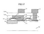
- FIGS. 15 and 16show an SRAM cell layout MC 7 in accordance with Embodiment 8. An explanation of those symbols used in FIGS. 15 - 16 is given at lower part of FIG. 16.
- Memory cell MC 7 of Embodiment 8is similar to the memory cell MC of Embodiment 1 with the contacts (SC 1 , SC 2 ) being replaced with local interconnect nodes (LI 1 , LI 2 ) and also with the word lines being modified in such a manner that these are formed in the first layer of metal lead layer rather than in the second layer of metal lead layer while also modifying the bit lines and power supply and ground lines from the third layer of metal lead layer to the second layer of metal lead layer.
- FIG. 17depicts a sectional view taken along line A-B of FIGS. 15 - 16 .
- Embodiment 1suffers from limitations as to an inability to dispose the first layer of metal leads over the contacts SC 1 , SC 2 due to the fact that these contacts SC 1 , SC 2 are formed of the same layer as the remaining contacts used.
- Embodiment 8is specifically arranged to employ the local interconnect nodes LI 1 , LI 2 formed in a separate layer from the contacts, thus making it possible to dispose the first layer of metal lead layer at upper part, which in turn makes it possible to reduce by one the requisite number of metal lead layers when compared to Embodiment 1.
- FIGS. 18 a - 18 fA process flow of major steps in the manufacture of a three-layer contact section of Embodiment 9 is shown in FIGS. 18 a - 18 f.
- This embodiment 9is an example of the process for fabrication of the three-layer contact section as used in Embodiments 1, 3-5 and 8.
- Embodiment 9is for enabling achievement of electrical conduction of such contacts overlying gate electrodes by previous removal of any silicon nitride film portions overlying gate electrodes at specified part whereat contact holes will be defined.
- a silicon nitride film SiNfor use as an etch stopper (FIG. 18 a ).
- the gate electrodeis a lamination of polycrystalline silicon PolySi and tungsten W, with an oxide film SiO being further multilayered thereon as a protective film.
- FIGS. 19 a - 19 gthere is shown a process flow in the manufacture of the three-layer contact section of Embodiment 10.
- Embodiment 10is one example of the process for forming the three-layer contact section of Embodiments 1, 3-5 and 8.
- a difference of the process flow of Embodiment 10 from that of Embodiment 9is that more than one portion of the oxide film at a specified location whereat a contact hole is to be opened over the gate electrode has been removed in advance prior to deposition of a silicon nitride film for use as the etch stopper.
- Embodiment 10The fabrication process flow of Embodiment 10 will be explained with reference to FIGS. 19 a - 19 g below.
- the gate electrodeis a lamination of polycrystalline silicon PolySi and tungsten W, with an oxide film SiO further stacked thereon as a protective film.
- any diffusion layers used thereinare specifically designed to have a simplified planar shape excluding unnecessarily complicated shapes, which may in turn facilitate micro-patterning processes.
Landscapes
- Engineering & Computer Science (AREA)
- Microelectronics & Electronic Packaging (AREA)
- Computer Hardware Design (AREA)
- Semiconductor Memories (AREA)
Abstract
Description
- The present invention relates generally to semiconductor integrated circuit devices and, more particularly, to layout schemes of static random access memory (SRAM) cells. The invention also relates to semiconductor memory devices using such cells.[0001]
- One-port SRAM cells with complementary metal oxide semiconductor (CMOS) configurations are typically designed so that each cell consists essentially of six separate transistors. An exemplary layout of such cells has been disclosed in, for example, JP-A-10-178110 (laid open on Jun. 30, 1998).[0002]
- In the prior known SRAM cell layout, a semiconductive well region of P type conductivity with inverters formed therein is subdivided into two subregions, which are disposed on the opposite sides of an N-type well region while permitting a well boundary line to extend in a direction parallel to bit lines.[0003]
- The quest for higher integration and ultra-fine patterning techniques in modern memory devices requires optical exposure apparatus or equipment to decrease in wave length of beams used therein. To this end, the equipment is designed to employ exposure beams of shorter wavelength, which have advanced from G line to I line, and further to excimer laser. Unfortunately the requirements for micro-patterning architectures grows more rapidly than technological advance in trend of shortening wavelengths in such equipment. In recent years, it is strictly required that micropatterning is done with the minimum device-feature length that shrinks to less than or equal to the wavelength of an exposure beam used. This minimum feature length shrinkage would result in the layout of IC components-here, memory cells-becoming more complicated in planar shape, which must require the use of irregular polygonal layout patterns including key-shaped components, in order to achieve the intended configuration of on-chip circuitry with enhanced accuracy. This makes it impossible or at least very difficult to microfabricate ultrafine layout patterns while disadvantageously serving as the cause of destruction of the symmetry of memory cells.[0004]
- Regrettably the prior art approach is associated with a need to curve or bend a diffusion layer into a complicated key-like shape for the purpose of making electrical contact with a substrate of the P-type well region. Thus, the prior art suffers from a problem as to degradation of the symmetrization of cell layout pattern, making difficult successful achievement of microfabrication architectures for higher integration densities.[0005]
- In accordance with one aspect of the present invention, a semiconductor device is provided which comprises a first inverter including a first N-channel metal oxide semiconductor (MOS) transistor and a first P-channel MOS transistor, a second inverter including a second N-channel MOS transistor and a second P-channel MOS transistor with an input terminal being connected to an output terminal of the first inverter and with an output terminal being connected to an input terminal of said first inverter, a third N-channel MOS transistor having a source connected to the output terminal of said first inverter and a drain connected to a first bit line and also a gate connected to a word line, and a fourth N-channel MOS transistor having a source connected to the output terminal of said second inverter and a drain connected to a second bit line plus a gate connected to a word line, wherein the first and third N-channel MOS transistors are formed in a first P-type well region, wherein the diffusion layer has no curved or bent portions while letting the direction of layout be parallel to the boundary with respect to the first N-well region with the first and second P-channel MOS transistors formed therein, and wherein said second and fourth N-channel MOS transistors are formed in the second P-type well region whose diffusion layer has no bent portions while letting the layout direction be parallel to the boundary with respect to the first N-well region with the first and second P-channel MOS transistors formed therein.[0006]
- The diffusion layer is arranged to have its outer shape that mainly consists of straight line segments including the longest straight line portion which lies parallel to the boundary with respect to the first n-well region with the first and second P-channel MOS transistors formed therein, and simultaneously in the case of defining a straight line acting as the center line extending parallel to such boundary, the longest line portion is in linear symmetry with such center line; the second and fourth N-channel MOS transistors are formed in the second P-well region whose diffusion layer is mainly arranged by straight line segments including its longest straight line portion that is parallel to the boundary with respect to the first n-well region with the first and second P-channel MOS transistors formed therein while allowing, when defining a straight line for use as the center line extending parallel to such boundary, the line portion to be linearly symmetrical with the center line. At this time, in the case of employing the linear symmetrization scheme, complete linear symmetry will not always be required; alternatively, slight nonsymmetry may also be permissible on a case-by-case basis, which nonsymmetry results from modifying the diffusion layer to have a shape with its portions on the right and left sides of the center line being substantially the same in area as each other by way of example.[0007]
- In accordance with another aspect of this invention, a first polycrystalline silicon lead layer for use as the gate of said third N-channel MOS transistor and a second polycrystalline silicon lead layer for use as the gate of said first P-channel MOS transistor and also as the gate of said first N-channel MOS transistor are disposed in parallel to each other, wherein a third polycrystalline silicon lead layer for use as the gate of said fourth N-channel MOS transistor and a fourth polycrystalline silicon lead layer for use as the gate of said second N-channel MOS transistor and also as the gate of said second P-channel MOS transistor are disposed in parallel to each other, and wherein the first and third polycrystalline silicon lead layers are connected via a contact to a second layer of metal lead layer constituting word lines.[0008]
- In accordance with a further aspect of the invention, the input terminal of said first inverter and the output terminal of said second inverter may be electrically connected together at a contact whereas the input terminal of said second inverter and the output terminal of said first inverter are electrically connected together at a contact.[0009]
- In accordance with yet another further aspect of the invention, a power supply line connected to the first and second bit lines and the sources of said first and second P-channel MOS transistors and a ground line connected to the sources of said first and second N-channel MOS transistors may be formed of a third layer of metal lead layer lying parallel to a diffusion layer.[0010]
- In accordance with a still another aspect of the invention, the first bit line formed of said third layer of metal lead layer may be arranged so that it is between a power supply line formed of said third layer of metal lead layer and a ground line as connected to the source of said first N-channel MOS transistor formed of said third layer of metal lead layer whereas the second bit line formed of said third layer of metal lead layer is between a power supply line formed of said third layer of metal lead layer and a ground line as connected to the source of said second N-channel MOS transistor formed of said third layer of metal lead layer.[0011]
- In accordance with another further aspect of the invention, the first and second bit lines and a power supply line connected to the sources of said first and second P-channel MOS transistors may be formed of a second layer of metal lead layer, wherein word lines are formed of a third layer of metal lead layer, and wherein a ground line connected to the sources of said first and second N-channel MOS transistors is formed of the third layer and second layer of metal lead layer.[0012]
- In accordance with a still another further aspect of the invention, memory cells are laid out into the form of an array, wherein contacts to a substrate of P-type well region and a contact to a substrate of N-type well region are linearly disposed within the array and at upper and lower portions of the array in a direction parallel to the word lines. Although the above is an example which causes two separate P-well to be disposed on the opposite sides of an N-well region, two N-well regions may be disposed on the opposite sides of a p-well region when the need arises.[0013]
- In accordance with yet another further aspect of the invention, a semiconductor device is provided which comprises a plurality of memory arrays each including an array of memory cells each having at least a pair of N-type well region and P-type well region, and at least one intermediate region between the memory arrays, wherein the N-type well region and P-type well region defines therebetween a boundary with at least one straight line portion, and wherein a diffusion layer is formed in each of the P-type well region and P-type well region to have a planar shape of either (1) a shape of rectangle having long sides extending parallel to said straight line portion or (2) a shape resulting from letting a plurality of rectangles having long sides extending parallel to the straight line portion be combined together via respective short sides thereof; or alternatively,[0014]
- (1) a shape of rectangle having long sides parallel to said straight line portion or (2) a shape resulting from letting a plurality of rectangles having long sides parallel to said straight line portion be combined together causing them to extend in the direction of the straight line.[0015]
- At least in memory array regions, bit lines are laid out in a direction parallel to the straight line portion whereas word lines are disposed in a direction perpendicular to the straight portion. Preferably, in the intermediate region, at least one type of electrical lead is railed in a direction at right angles to the straight portion, and a lead (e.g. contact) is also formed which is for making electrical contact between a power supply voltage lead and the diffusion layer as formed in the N-well region or P-well region. This lead may include a power supply lead, ground lead, or other potential leads.[0016]
- The invention is particularly useful for those semiconductor memory devices having static RAM memory cells each consisting essentially of six separate transistors.[0017]
- FIG. 1 is a diagram showing an SRAM cell in accordance with[0018]
Embodiment 1 of the present invention, for explanation of a layout pattern of those contacts for connection between MOS transistors and those for connecting between MOS transistors and metal lead layers. - FIG. 2 is a diagram showing a layout of via holes of SRAM cells for connection between multilayered metal leads in accordance with[0019]
Embodiment 1 of this invention - FIG. 3 is a diagram showing a layout of memory cells and their associated peripheral circuitry in accordance with[0020]
Embodiment 2 of the invention. - FIG. 4 is a diagram showing an SRAM cell in accordance with Embodiment 3 of the invention, for explanation of a layout of those contacts for connection between MOS transistors and thosoe for connection between MOS transistor and metal lead layers.[0021]
- FIG. 5 is a diagram showing a layout of via holes of SRAM cells for connection between multilayered metal leads in accordance with Embodiment 3 of the invention.[0022]
- FIG. 6 is a diagram showing an SRAM cell in accordance with Embodiment 4 of the invention, for explanation of a layout of those contacts for connection between MOS transistors and those for connection between MOS transistors and metal lead layers.[0023]
- FIG. 7 is a diagram showing a layout of via holes of SRAM cells for connection between multilayered metal leads in accordance with Embodiment 3 of the invention.[0024]
- FIG. 8 is a diagram showing an SRAM cell in accordance with Embodiment 5 of the invention, for explanation of a layout of those contacts for connection between MOS transistors and those for connection between MOS transistors and metal lead layers.[0025]
- FIG. 9 is a diagram showing a layout of via holes of SRAM cells for connection between multilayered metal leads in accordance with Embodiment 5 of the invention.[0026]
- FIG. 10 is a diagram showing an SRAM cell in accordance with Embodiment 6 of the invention, for explanation of a layout of those contacts for for connection between MOS transistors and those for connection between MOS transistors and metal lead layers.[0027]
- FIG. 11 is a diagram showing a layout of via holes of SRAM cells for connection between multilayered metal leads in accordance with Embodiment 6 of the invention.[0028]
- FIGS. 12[0029]ato12fare diagrams illustrating in cross-section some of major process steps in the manufacture of the semiconductor device in accordance with Embodiment 6 of the invention.
- FIG. 13 is a diagram showing an SRAM cell in accordance with Embodiment 7 of the invention, for explanation of a layout of those contacts for connection between MOS transistors and those for connection between MOS transistors and metal lead layers.[0030]
- FIG. 14 is a diagram showing a layout of via holes of SRAM cells for use in connecting between multilayered metal leads in accordance with Embodiment 7 of the invention.[0031]
- FIG. 15 is a diagram showing an SRAM cell in accordance with Embodiment 8 of the invention, for explanation of a layout of those contacts for connection between MOS transistors and those for connection between MOS transistors and metal lead layers.[0032]
- FIG. 16 is a diagram showing a layout of via holes of SRAM cells for connection between multilayered metal leads in accordance with Embodiment 8 of the invention.[0033]
- FIG. 17 is a sectional view of a semiconductor device in accordance with Embodiment 8 of the invention.[0034]
- FIGS. 18[0035]ato18fare diagrams illustrating in cross-section some of major process steps in the manufacture of a semiconductor device in accordance with Embodiment 9 of the invention.
- FIGS. 19[0036]ato19gare diagrams illustrating in cross-section some of major process steps in the manufacture of a semiconductor device in accordance with Embodiment 10 of the invention.
- Several preferred embodiments of the semiconductor memory device in accordance with the present invention will be explained with reference to the accompanying drawings below.[0037]
- <[0038]
Embodiment 1> - Referring to FIGS. 1 and 2, there is shown an SRAM cell layout MC embodying the invention. FIG. 1 illustrates well regions and diffusion layers plus polycrystalline silicon interconnect lead layer as well as contacts, all of which are formed in or over a semiconductor substrate whereas FIG. 2 depicts a first layer of metal lead layer, via[0039]
holes 1, second layer of metal lead layer, viaholes 2, and a third layer of metal lead layer. Symbols used in FIGS. 1 and 2 are indicated at lower part of FIG. 2. - An N-channel type MOS transistor TN[0040]1 formed in a P-type semiconductive well region PW1 and a P-channel type MOS transistor TP1 formed in an N-type well region NW1 constitute an inverter INV1. In addition, an N-channel MOS transistor TN2 formed in P-type well region PW2 and a P-channel MOS transistor TP2 formed in N-type well region NW1 constitute an inverter INV2.
- An output node of the inverter INV[0041]1 is electrically connected by a contact SC1 to an input node of the inverter INV2. An output of the inverter INV2 is electrically connected via a contact SC2 to an input of the inverter INV1.
- An N-channel MOS transistor TN[0042]3 has a drain electrode connected to a bit line BL1, a source electrode connected to a drain of the N-channel MOS transistor TN1, and a gate electrode connected to a word line WD. Similarly an N-channel MOS transistor TN4 has a drain electrode connected to a bit line BL2, a source electrode connected to a drain of the N-channel MOS transistor TN2, and a gate electrode connected to word line WD.
- The N-channel MOS transistor TN[0043]1 and N-channel MOS transistor TN3 are formed over a diffusion layer LN1 whereas the N-channel MOS transistor TN2 and N-channel MOS transistor TN4 are formed over a diffusion layer LN2. The P-channel MOS transistor TP1 is formed over a diffusion layer LP1 whereas the P-channel MOS transistor TP2 is formed over a diffusion layer LP2.
- As the diffusion layers (LN[0044]1, LN2, LP1, LP2) are straight lines with no curved portions, any pattern correction at folded portions is no longer necessary, resulting in the balance between nodes being improved. In case memory cells are laid out into the form of an array, the diffusion layers become four separate straight lines extending parallel to the bit lines (BL1, BL2).
- In addition, a polycrystalline silicon interconnect lead layer FG[0045]3 for use as the gate electrode of the N-channel MOS transistor TN3 and a polycrystalline silicon lead layer FG4 for use as the gate electrode of N-channel MOS transistor TN4 are connected to word lines WL which are formed of the second metal lead layer in a vertical direction to the bit lines (BL1, BL2). A polycrystalline silicon interconnect lead layer FG1 for use as the gate electrodes of the N-channel MOS transistor TN1 and P-channel MOS transistor TP1 and a polycrystalline silicon interconnect lead layer FG2 for use as the gate electrode of the N-channel MOS transistor TN2 and P-channel MOS transistor TP2 plus the polycrystalline silicon lead layers (FG3, FG4) are disposed in parallel to the word lines.
- The N-channel MOS transistor TN[0046]1 has its source electrode connected to a ground potential line Vss1 that is formed of the third layer of metal lead layer whereas a source electrode of the N-channel MOS transistor TN2 is connected to a ground line Vss2 as formed of the third layer of metal lead layer. In addition, source electrodes of the P-channel MOS transistors (TP1, TP2) are connected to a power supply voltage line Vcc1 which is formed of the third layer of metal lead layer.
- The bit line BL[0047]1 is located midway between the power supply voltage line Vcc1 and ground line Vss1 whereas bit line BL2 is between the supply voltage line Vcc1 and ground line Vss2. This structure makes it possible to reduce cross-couple noises occurring between bit lines, which advantageously lowers voltages while increasing operation speeds.
- In addition, it is considered that, in case a contact is formed on an n[0048]− layer through partial cutaway of side spacers during etching of contact holes, a leakage current from the contact via the n− layer to the substrate may be produced. When a contact is formed for connection between a polycrystalline silicon lead layer and a diffusion layer, a distance between the diffusion layer LP2 and polycrystalline silicon lead layer FG1 should be greater than the length of a side spacer to thereby eliminate formation an n− layer on the polycrystalline silicon lead layer FG1 side of the diffusion layer LP2, which in turn makes it possible to prevent a flow of leakage current.
- <[0049]
Embodiment 2> - Turning to FIG. 3, there is shown an exemplary case where the memory cells MC of[0050]
Embodiment 1 are laid out into the form of an array. Symbols used herein are the same as those indicated at lower part of FIG. 2. - The memory cells MC are organized into an array of 256 rows and 128 columns, by way of example. In view of the fact that these memory cells in[0051]
Embodiment 1 are less in length in the longitudinal direction of bit lines, a total length of such 256 rows of memory cells along the bit lines is shorter than that of prior art devices, thus increasing resultant operation speeds. Neighboring memory cells MC are disposed in linear symmetry with respect to a “y” axis whereas upper and lower adjacent memory cells MC are in linear symmetry with an “x” axis. In addition, specified regions ST for use in supplying more than one power supply voltage to the substrate are formed at intermediate part of the array in such a manner that the regions ST extend parallel to word lines WD. One example is that the regions ST are laid out in units of 32-row groups. Another example is that regions ST are disposed in units of 64-row groups. - An electrical lead Vbn for supplying a voltage potential to the P-well regions (PW[0052]1, PW2) and a lead Vbp for supplying a voltage to the N-well region NW1 are formed to lie parallel to word lines. The lead Vbn may be coupled to ground potential Vss or, alternatively, any voltage may be applied thereto which is potentially different from ground Vss. The lead Vbp may be coupled to the power supply voltage Vcc or, alternatively, any voltages potentially different from Vcc may be applied thereto.
- Note that in each region ST, a power supply voltage line Vcc for potentially “reinforcing” a power supply voltage line Vcc[0053]1 is formed in parallel to word lines while letting a ground potential line Vss for potentially reinforcing ground potentials (Vss1, Vss2) is formed in parallel to the word lines.
- Also note that the ground lines (Vss[0054]1, Vss2) are disposed in a direction perpendicular to the word lines WD whereby upon selecting of a single word line a voltage potential is supplied from the pair of ground lines to a respective one of those memory cells operatively associated with this selected word line so that any possible noises occurring at such voltage lines are reduced to thereby advantageously speed up an access operation while potentially reducing any voltages concerned.
- Furthermore, the memory cells MC used are great in width in the word line direction so that the layout design of sense amplifiers AMP is made easier to thereby avoid a need to lay out one sense amplifier for two adjacent columns of memory cells, which in turn makes it possible to permit one sense amplifier to be laid out at each column. Additionally a word line driver circuit wddrv becomes flat in layout as compared to prior known ones.[0055]
- <Embodiment 3>[0056]
- FIGS. 4 and 5 show a SRAM cell layout MC[0057]2 in accordance with Embodiment 3. Symbols as used in FIGS.4-5 are the same as those in FIG. 2. Memory cell MC2 of Embodiment 3 is similar to the memory cell MC of
Embodiment 1, except that whereas inEmbodiment 1 the diffusion layer (LN1, LN2) is formed into a “IT”-like planar shape, which resembles a Japanese battledore plate called “hagoita,” the diffusion layer (LN3, LN4) of Embodiment 4 is of a rectangular shape, and that the contacts (SC1, SC2) are replaced with contacts (SC3, SC4) in the first layer of metal lead layers (M11, M12). - To attain stability, memory cells are typically designed so that the gate width of N-channel MOS transistors (TN[0058]1, TN2) is one and a half times greater than that of N-channel MOS transistors (TN3, TN4) However, in this case, the shape of diffusion layers resembles a T- like planar shape as has been shown in
Embodiment 1, which in turn requires extra techniques including pattern correction procedures such as optical proximity effect correction (OPC) processes. Additionally this would result in degradation of the balance between transistors. In contrast, Embodiment 3 is such that the diffusion layers (LN3, LN4) are designed to have a rectangular shape whereby the micro-patterning required becomes easier while at the same time enabling improvement in balance between transistors. Note however that the resultant gate width ratio becomes as large as 1.0 time, which in turn requires that the so-called cell ratio be increased by making different drivabilities therebetween, which is achievable by letting the N-channel MOS transistors (TN3, TN4) be greater in oxide film thickness than N-channel MOS transistors (TN1, TN2), or by increasing the gate length thereof, or alternatively by increasing the threshold value, or still alternatively by lowering the impurity concentration of lightly-doped drain regions for relaxation of electric fields. - In addition, Embodiment 3 is arranged to employ a contact SC[0059]3 and a first layer of metal lead layer M11 in place of the contact SC1 used in
Embodiment 1 for connection between the output of inverter INV1 and the input of inverter INV2. With such an arrangement, any curved or bent contacts are no longer necessary, thereby avoiding the need for pattern correction (OPC) or the like. - <Embodiment 4>[0060]
- FIGS. 6 and 7 show an SRAM cell layout MC[0061]3 in accordance with an embodiment4. Symbols as used in FIGS.6-7 are the same as those in FIG. 2. Memory cell MC3 of Embodiment 4 is similar to the memory cell MC2 of Embodiment 3 except that polycrystalline silicon lead layers (FG5, FG6, FG7, FG8) are designed to have a rectangular planar shape. With this cell, any bent/folded portions are absent thus removing the need for any additional pattern correction procedures including OPC processes, which in turn improves the balance between transistors.
- <Embodiment 5>[0062]
- FIGS. 8 and 9 show an SRAM cell layout MC[0063]4 in accordance with Embodiment 5. An explanation on those symbols used in FIGS. 8 and 9 is given at lower part of FIG. 8. Memory cell MC4 of Embodiment 5 is different in lead structure from the memory cell MC of
Embodiment 1. - Bit lines (BL[0064]3, BL4) and power supply line Vcc2 are formed by use of a second layer of metal lead layer. A word line WD1 and ground lines (Vss5, Vss6) are formed using a third layer of metal lead layer in a perpendicular direction to the bit lines. Ground lines (Vss3, Vss4) are formed using a fourth layer of metal lead layer in a direction parallel to the bit lines.
- A global bit line GB is the electrical interconnect lead that is used in case bit lines are of a hierarchical configuration. The global bit line GB and bit lines (BL[0065]3, BL4) are shielded by the third layer of metal lead layer, thus enabling prevention of any possible cross-couple noises. Additionally the use of ground lines (Vss3, Vss4) makes it possible to prevent occurrence of cross-couple noises between global bit lines GB.
- <Embodiment 6>[0066]
- FIGS. 10 and 11 show an SRAM cell layout MC[0067]5 in accordance with an embodiment6. An explanation as to those symbols used in FIGS.10-11 is given at lower part of FIG. 11. Memory cell MC5 of Embodiment 6 is different from the memory cell MC of
Embodiment 1 in structure of the so-called three-layered contacts, each of which is for connection between a gate electrode and its associated diffusion layer. - Although in Embodiment 1 a gate electrode is connected to a diffusion layer via “L”-like contacts SC[0068]1, SC2, Embodiment 6 is arranged so that the gate electrode is connected to the diffusion layer via silicide in connect regions SS1, SS2. This makes it unnecessary to bend or curve the individual contact into the L-like shape in order to connect the gate electrode to the diffusion layer, which in turn makes it possible to provide “I”-like rectangular contacts SC5, SC6. No folded/bent portions are present in the contacts used, which eliminates the need for pattern correction (OPC).
- One practically implementable flow of some major process steps in the manufacture of a device structure employing the connect regions SS[0069]1, SS2 each for connection between a gate electrode and a diffusion layer associated therewith via silicide is shown in FIGS. 12athrough12f.Note here that FIGS. 12a-12fare cross-sectional views each indicating a profile as taken along line A-A′ in FIG. 10, with its right side corresponding to the side “A” and with left side corresponding to “A′.”
- Fabricate a gate electrode FG made of a chosen polycrystalline silicon material (see FIG. 12[0070]a).
- Form a heavily-doped diffusion layer PM of a specified conductivity type-here, P type (FIG. 12[0071]b).
- Form side spacers made of silicon nitride (SiN) by chemical vapor deposition (CVD) techniques, on sidewalls of the resultant gate electrode FG (FIG. 12[0072]c).
- Make use of a resist RG to etch away only one of the SiN side spacers which resides on an active region side under a prespecified condition that enables etching treatment of a silicon nitride film and oxide film at increased selectivity (FIG. 12[0073]d).
- Fabricate a heavily-doped P (P+) type diffusion layer P+.[0074]
- After having removed through etching certain part of the oxide film SiO that lies in the active region that is not covered by any overlying gate electrode FG, deposit a high-melting-point metal such as refractory metal including, but not limited to, cobalt (Co); then, anneal the resultant structure to thereby selectively form silicide on the poly-silicon gate electrode and diffusion layer (FIG. 12[0075]f). At this time the gate electrode's sidewall and diffusion layer are connected together by such silicide.
- <Embodiment 7>[0076]
- FIGS. 13 and 14 show an SRAM cell layout MC[0077]6 in accordance with Embodiment 7. An explanation of those symbols used in FIGS.13-14 is the same as that given at lower part of FIG. 11. Memory cell MC6 of Embodiment 7 is similar to the memory cell MC5 of Embodiment 6 with the contacts (SC5, SC6) being replaced with contacts (SC7, SC8) in the first layer of metal lead layers (M11, M12).
- With Embodiment 7, all of the contacts used therein are capable of being designed to have a square planar shape, thus avoiding the need for pattern correction (OPC).[0078]
- <Embodiment 8>[0079]
- FIGS. 15 and 16 show an SRAM cell layout MC[0080]7 in accordance with Embodiment 8. An explanation of those symbols used in FIGS.15-16 is given at lower part of FIG. 16. Memory cell MC7 of Embodiment 8 is similar to the memory cell MC of
Embodiment 1 with the contacts (SC1, SC2) being replaced with local interconnect nodes (LI1, LI2) and also with the word lines being modified in such a manner that these are formed in the first layer of metal lead layer rather than in the second layer of metal lead layer while also modifying the bit lines and power supply and ground lines from the third layer of metal lead layer to the second layer of metal lead layer. FIG. 17 depicts a sectional view taken along line A-B of FIGS.15-16. - [0081]
Embodiment 1 suffers from limitations as to an inability to dispose the first layer of metal leads over the contacts SC1, SC2 due to the fact that these contacts SC1, SC2 are formed of the same layer as the remaining contacts used. In contrast, Embodiment 8 is specifically arranged to employ the local interconnect nodes LI1, LI2 formed in a separate layer from the contacts, thus making it possible to dispose the first layer of metal lead layer at upper part, which in turn makes it possible to reduce by one the requisite number of metal lead layers when compared toEmbodiment 1. - <Embodiment 9>[0082]
- A process flow of major steps in the manufacture of a three-layer contact section of Embodiment 9 is shown in FIGS. 18[0083]a-18f.This embodiment 9 is an example of the process for fabrication of the three-layer contact section as used in
Embodiments 1, 3-5 and 8. - Modern LSIs in recent years are typically designed so that micropatterning is done to form contact holes by high-selectivity etching techniques with a silicon nitride film or else used as a stopper to ensure that any unwanted over-etching occurs at filed oxide films even when contacts are offset in position from diffusion layers and/or gate electrodes due to the presence of possible alignment errors during photolithographical patterning processes. In cases gate electrodes are formed to have reduced electrical resistivities by use of the so-called salicide processes, it is possible to obtain the intended electrical conduction between a contact lying over a gate electrode and a contact overlying a diffusion layer even when the both contacts are fabricated at a time because of the fact that the contact holes required are fabricated after completion of a procedure having the steps of forming silicide through exposure of selected portions overlying diffusion layers and gate electrodes after having formed such diffusion layers, depositing thereover a silicon nitride film for use as an etching stopper, and then further depositing thereover an interlayer dielectric film. On the contrary, in the case of either traditionally widely employed polycide gate electrodes or polymetal gate electrodes that have been developed and announced recently, residual portions of an insulative film such as oxide film can overlie gate electrodes thereby preventing exposure of these gate electrodes prior to deposition of a silicon nitride film acting as the etch stopper; accordingly, whenever an attempt is made to form the intended contacts through deposition of a silicon nitride film thereover, the oxide film behaves to partly reside at the bottom of a respective one of those contacts overlying the gate electrodes, which makes it impossible or at least greatly difficult to provide electrical conduction required. Embodiment 9 is for enabling achievement of electrical conduction of such contacts overlying gate electrodes by previous removal of any silicon nitride film portions overlying gate electrodes at specified part whereat contact holes will be defined.[0084]
- An explanation will now be given of the process flow in the manufacture of Embodiment 9 with reference to FIGS. 18[0085]a-18fbelow.
- After having fabricated a gate electrode and a diffusion layer P+, deposit a silicon nitride film SiN for use as an etch stopper (FIG. 18[0086]a). The gate electrode is a lamination of polycrystalline silicon PolySi and tungsten W, with an oxide film SiO being further multilayered thereon as a protective film.
- Remove by dry etching techniques specified part of the silicon nitride film at locations for definition of a contact hole overlying the gate electrode (FIG. 18[0087]b).
- Deposit a TEOS film and others by plasma CVD methods to thereby form an interlayer dielectric film (FIG. 18[0088]c).
- Let a selected portion of the oxide film at a contact opening portion be etched away by high selective dry etching techniques (FIG. 18d). Owing to such high selective etching, the silicon nitride film remains free from etch treatment and thus acts as a stopper. Since there is no stopper at the portion overlying the gate electrode from which the silicon nitride film has been removed away in advance, such portion will be fully etched to the upper part of the gate electrode. This permits electrical conduction on the gate electrode also.[0089]
- Remove the silicon nitride film by dry etching techniques (FIG. 18[0090]e). Deposit a chosen metal such as tungsten in the resulting contact hole, thereby forming a buried plug (FIG. 18f).
- <Embodiment 10>[0091]
- Turning to FIGS. 19[0092]a-19g,there is shown a process flow in the manufacture of the three-layer contact section of Embodiment 10. Embodiment 10 is one example of the process for forming the three-layer contact section of
Embodiments 1, 3-5 and 8. - A difference of the process flow of Embodiment 10 from that of Embodiment 9 is that more than one portion of the oxide film at a specified location whereat a contact hole is to be opened over the gate electrode has been removed in advance prior to deposition of a silicon nitride film for use as the etch stopper.[0093]
- The fabrication process flow of Embodiment 10 will be explained with reference to FIGS. 19[0094]a-19gbelow.
- Fabricate a gate electrode and a diffusion layer P+ (FIG. 19[0095]a). The gate electrode is a lamination of polycrystalline silicon PolySi and tungsten W, with an oxide film SiO further stacked thereon as a protective film.
- Remove by dry etching techniques a specified part of the silicon nitride film at the location for definition of a contact hole overlying the gate electrode, thus letting the gate electrode be exposed at its upper part (FIG. 19[0096]b).
- Deposit a silicon nitride film SiN as an etch stopper (FIG. 19[0097]c).
- Deposit a TEOS film or else by plasma CVD methods to thereby form an interlayer dielectric film (FIG. 19[0098]d).
- Let a portion of the oxide film at contact opening portion be etched away by high selective dry etching techniques (FIG. 19[0099]e). Due to such high selective etching, the silicon nitride film remains free from etching treatment and thus acts as the stopper. Remove the silicon nitride film by dry etching techniques (FIG. 19f). A certain portion from which the oxide film overlying the gate electrode has been removed prior to deposition of the silicon nitride film is thus exposed at this time, which permits electrical conduction on the gate electrode also.
- Deposit a chosen metal such as tungsten in the resultant contact hole, thereby forming a buried plug (FIG. 19[0100]g).
- In accordance with the embodiments stated above, any diffusion layers used therein are specifically designed to have a simplified planar shape excluding unnecessarily complicated shapes, which may in turn facilitate micro-patterning processes.[0101]
Claims (29)
Priority Applications (10)
| Application Number | Priority Date | Filing Date | Title |
|---|---|---|---|
| US10/606,954US20040012040A1 (en) | 1999-05-12 | 2003-06-27 | Semiconductor integrated circuit device |
| US11/042,172US7612417B2 (en) | 1999-05-12 | 2005-01-26 | Semiconductor integrated circuit device |
| US11/261,764US20060050588A1 (en) | 1999-05-12 | 2005-10-31 | Semiconductor integrated circuit device |
| US12/348,524US7781846B2 (en) | 1999-05-12 | 2009-01-05 | Semiconductor integrated circuit device |
| US12/821,329US8482083B2 (en) | 1999-05-12 | 2010-06-23 | Semiconductor integrated circuit device including SRAM memory cells having two P-channel MOS transistors and four N-channel MOS transistors and with four wiring layers serving as their gate electrodes |
| US13/616,435US9286968B2 (en) | 1999-05-12 | 2012-09-14 | Semiconductor integrated circuit device including SRAM cell array and a wiring layer for supplying voltage to well regions of SRAM cells provided on a region exterior of SRAM cell array |
| US14/752,514US9449678B2 (en) | 1999-05-12 | 2015-06-26 | Semiconductor integrated circuit device |
| US15/216,327US9646678B2 (en) | 1999-05-12 | 2016-07-21 | Semiconductor integrated circuit device |
| US15/448,585US9985038B2 (en) | 1999-05-12 | 2017-03-02 | Semiconductor integrated circuit device |
| US15/975,761US20180261607A1 (en) | 1999-05-12 | 2018-05-09 | Semiconductor integrated circuit device |
Applications Claiming Priority (3)
| Application Number | Priority Date | Filing Date | Title |
|---|---|---|---|
| JP13094599 | 1999-05-12 | ||
| JP11-130945 | 1999-05-12 | ||
| JP2000132848AJP4565700B2 (en) | 1999-05-12 | 2000-04-27 | Semiconductor device |
Related Child Applications (1)
| Application Number | Title | Priority Date | Filing Date |
|---|---|---|---|
| US10/606,954ContinuationUS20040012040A1 (en) | 1999-05-12 | 2003-06-27 | Semiconductor integrated circuit device |
Publications (2)
| Publication Number | Publication Date |
|---|---|
| US20020117722A1true US20020117722A1 (en) | 2002-08-29 |
| US6677649B2 US6677649B2 (en) | 2004-01-13 |
Family
ID=15046349
Family Applications (11)
| Application Number | Title | Priority Date | Filing Date |
|---|---|---|---|
| US09/565,535Expired - LifetimeUS6677649B2 (en) | 1999-05-12 | 2000-05-05 | SRAM cells with two P-well structure |
| US10/606,954AbandonedUS20040012040A1 (en) | 1999-05-12 | 2003-06-27 | Semiconductor integrated circuit device |
| US11/042,172Expired - Fee RelatedUS7612417B2 (en) | 1999-05-12 | 2005-01-26 | Semiconductor integrated circuit device |
| US11/261,764AbandonedUS20060050588A1 (en) | 1999-05-12 | 2005-10-31 | Semiconductor integrated circuit device |
| US12/348,524Expired - Fee RelatedUS7781846B2 (en) | 1999-05-12 | 2009-01-05 | Semiconductor integrated circuit device |
| US12/821,329Expired - Fee RelatedUS8482083B2 (en) | 1999-05-12 | 2010-06-23 | Semiconductor integrated circuit device including SRAM memory cells having two P-channel MOS transistors and four N-channel MOS transistors and with four wiring layers serving as their gate electrodes |
| US13/616,435Expired - Fee RelatedUS9286968B2 (en) | 1999-05-12 | 2012-09-14 | Semiconductor integrated circuit device including SRAM cell array and a wiring layer for supplying voltage to well regions of SRAM cells provided on a region exterior of SRAM cell array |
| US14/752,514Expired - Fee RelatedUS9449678B2 (en) | 1999-05-12 | 2015-06-26 | Semiconductor integrated circuit device |
| US15/216,327Expired - Fee RelatedUS9646678B2 (en) | 1999-05-12 | 2016-07-21 | Semiconductor integrated circuit device |
| US15/448,585Expired - Fee RelatedUS9985038B2 (en) | 1999-05-12 | 2017-03-02 | Semiconductor integrated circuit device |
| US15/975,761AbandonedUS20180261607A1 (en) | 1999-05-12 | 2018-05-09 | Semiconductor integrated circuit device |
Family Applications After (10)
| Application Number | Title | Priority Date | Filing Date |
|---|---|---|---|
| US10/606,954AbandonedUS20040012040A1 (en) | 1999-05-12 | 2003-06-27 | Semiconductor integrated circuit device |
| US11/042,172Expired - Fee RelatedUS7612417B2 (en) | 1999-05-12 | 2005-01-26 | Semiconductor integrated circuit device |
| US11/261,764AbandonedUS20060050588A1 (en) | 1999-05-12 | 2005-10-31 | Semiconductor integrated circuit device |
| US12/348,524Expired - Fee RelatedUS7781846B2 (en) | 1999-05-12 | 2009-01-05 | Semiconductor integrated circuit device |
| US12/821,329Expired - Fee RelatedUS8482083B2 (en) | 1999-05-12 | 2010-06-23 | Semiconductor integrated circuit device including SRAM memory cells having two P-channel MOS transistors and four N-channel MOS transistors and with four wiring layers serving as their gate electrodes |
| US13/616,435Expired - Fee RelatedUS9286968B2 (en) | 1999-05-12 | 2012-09-14 | Semiconductor integrated circuit device including SRAM cell array and a wiring layer for supplying voltage to well regions of SRAM cells provided on a region exterior of SRAM cell array |
| US14/752,514Expired - Fee RelatedUS9449678B2 (en) | 1999-05-12 | 2015-06-26 | Semiconductor integrated circuit device |
| US15/216,327Expired - Fee RelatedUS9646678B2 (en) | 1999-05-12 | 2016-07-21 | Semiconductor integrated circuit device |
| US15/448,585Expired - Fee RelatedUS9985038B2 (en) | 1999-05-12 | 2017-03-02 | Semiconductor integrated circuit device |
| US15/975,761AbandonedUS20180261607A1 (en) | 1999-05-12 | 2018-05-09 | Semiconductor integrated circuit device |
Country Status (4)
| Country | Link |
|---|---|
| US (11) | US6677649B2 (en) |
| JP (10) | JP4565700B2 (en) |
| KR (8) | KR100796215B1 (en) |
| TW (1) | TW469632B (en) |
Cited By (99)
| Publication number | Priority date | Publication date | Assignee | Title |
|---|---|---|---|---|
| US20030067819A1 (en)* | 2001-10-05 | 2003-04-10 | Matsushita Electric Industrial Co., Ltd. | Semiconductor memory device |
| US20030133322A1 (en)* | 2002-01-11 | 2003-07-17 | International Business Machines Coporation | Compact SRAM cell layout for implementing one-port or two-port operation |
| US20030189535A1 (en)* | 2002-04-04 | 2003-10-09 | Shoichiro Matsumoto | Semiconductor device and display apparatus |
| US6681379B2 (en)* | 2000-07-05 | 2004-01-20 | Numerical Technologies, Inc. | Phase shifting design and layout for static random access memory |
| US20060034141A1 (en)* | 2003-08-18 | 2006-02-16 | Fujitsu Limited | Nonvolatile semiconductor memory |
| US20070007603A1 (en)* | 2005-07-07 | 2007-01-11 | Takayuki Yamada | Semiconductor device |
| US20080123462A1 (en)* | 2006-11-29 | 2008-05-29 | Taiwan Semiconductor Manufacturing Co., Ltd. | Multiple-port SRAM device |
| EP1962345A2 (en) | 2007-02-23 | 2008-08-27 | Canon Kabushiki Kaisha | Photoelectric conversion apparatus with dual-damascene interconnections and image pickup system using the same |
| US20100033469A1 (en)* | 2004-12-15 | 2010-02-11 | Ignis Innovation Inc. | Method and system for programming, calibrating and driving a light emitting device display |
| US20110096586A1 (en)* | 2006-05-11 | 2011-04-28 | Renesas Electronics Corporation | Semiconductor memory device having layout area reduced |
| US20110294292A1 (en)* | 2010-05-25 | 2011-12-01 | Adetutu Olubunmi O | Method of forming a shared contact in a semiconductor device |
| CN103165575A (en)* | 2011-12-13 | 2013-06-19 | 格罗方德半导体公司 | Semiconductor device with transistor local interconnects |
| US20130193516A1 (en)* | 2012-01-26 | 2013-08-01 | Globalfoundries Inc. | Sram integrated circuits and methods for their fabrication |
| US8564513B2 (en) | 2006-01-09 | 2013-10-22 | Ignis Innovation, Inc. | Method and system for driving an active matrix display circuit |
| US8599191B2 (en) | 2011-05-20 | 2013-12-03 | Ignis Innovation Inc. | System and methods for extraction of threshold and mobility parameters in AMOLED displays |
| CN103681471A (en)* | 2012-09-14 | 2014-03-26 | 格罗方德半导体公司 | Bit cell with double patterned metal layer structure |
| US8743096B2 (en) | 2006-04-19 | 2014-06-03 | Ignis Innovation, Inc. | Stable driving scheme for active matrix displays |
| US8803417B2 (en) | 2009-12-01 | 2014-08-12 | Ignis Innovation Inc. | High resolution pixel architecture |
| US8860636B2 (en) | 2005-06-08 | 2014-10-14 | Ignis Innovation Inc. | Method and system for driving a light emitting device display |
| US8908420B2 (en) | 2012-06-08 | 2014-12-09 | Renesas Electronics Corporation | Semiconductor device |
| US8907991B2 (en) | 2010-12-02 | 2014-12-09 | Ignis Innovation Inc. | System and methods for thermal compensation in AMOLED displays |
| USRE45291E1 (en) | 2004-06-29 | 2014-12-16 | Ignis Innovation Inc. | Voltage-programming scheme for current-driven AMOLED displays |
| US8922544B2 (en) | 2012-05-23 | 2014-12-30 | Ignis Innovation Inc. | Display systems with compensation for line propagation delay |
| US8941697B2 (en) | 2003-09-23 | 2015-01-27 | Ignis Innovation Inc. | Circuit and method for driving an array of light emitting pixels |
| US8994617B2 (en) | 2010-03-17 | 2015-03-31 | Ignis Innovation Inc. | Lifetime uniformity parameter extraction methods |
| US9030506B2 (en) | 2009-11-12 | 2015-05-12 | Ignis Innovation Inc. | Stable fast programming scheme for displays |
| US20150129990A1 (en)* | 2010-02-09 | 2015-05-14 | Taiwan Semiconductor Manufacturing Company, Ltd. | Semiconductor device having elevated structure |
| US20150137836A1 (en)* | 2012-06-18 | 2015-05-21 | Postech Academy-Industry Foundation | Metal oxide semiconductor gas sensor having nanostructure and method for manufacturing same |
| US9093028B2 (en) | 2009-12-06 | 2015-07-28 | Ignis Innovation Inc. | System and methods for power conservation for AMOLED pixel drivers |
| US9093029B2 (en) | 2011-05-20 | 2015-07-28 | Ignis Innovation Inc. | System and methods for extraction of threshold and mobility parameters in AMOLED displays |
| US9111485B2 (en) | 2009-06-16 | 2015-08-18 | Ignis Innovation Inc. | Compensation technique for color shift in displays |
| US9125278B2 (en) | 2006-08-15 | 2015-09-01 | Ignis Innovation Inc. | OLED luminance degradation compensation |
| US9153172B2 (en) | 2004-12-07 | 2015-10-06 | Ignis Innovation Inc. | Method and system for programming and driving active matrix light emitting device pixel having a controllable supply voltage |
| US9171504B2 (en) | 2013-01-14 | 2015-10-27 | Ignis Innovation Inc. | Driving scheme for emissive displays providing compensation for driving transistor variations |
| US9171500B2 (en) | 2011-05-20 | 2015-10-27 | Ignis Innovation Inc. | System and methods for extraction of parasitic parameters in AMOLED displays |
| US9269322B2 (en) | 2006-01-09 | 2016-02-23 | Ignis Innovation Inc. | Method and system for driving an active matrix display circuit |
| US9275579B2 (en) | 2004-12-15 | 2016-03-01 | Ignis Innovation Inc. | System and methods for extraction of threshold and mobility parameters in AMOLED displays |
| US9280933B2 (en) | 2004-12-15 | 2016-03-08 | Ignis Innovation Inc. | System and methods for extraction of threshold and mobility parameters in AMOLED displays |
| US9305488B2 (en) | 2013-03-14 | 2016-04-05 | Ignis Innovation Inc. | Re-interpolation with edge detection for extracting an aging pattern for AMOLED displays |
| US9311859B2 (en) | 2009-11-30 | 2016-04-12 | Ignis Innovation Inc. | Resetting cycle for aging compensation in AMOLED displays |
| US9324268B2 (en) | 2013-03-15 | 2016-04-26 | Ignis Innovation Inc. | Amoled displays with multiple readout circuits |
| US9336717B2 (en) | 2012-12-11 | 2016-05-10 | Ignis Innovation Inc. | Pixel circuits for AMOLED displays |
| US9343006B2 (en) | 2012-02-03 | 2016-05-17 | Ignis Innovation Inc. | Driving system for active-matrix displays |
| US9351368B2 (en) | 2013-03-08 | 2016-05-24 | Ignis Innovation Inc. | Pixel circuits for AMOLED displays |
| US9370075B2 (en) | 2008-12-09 | 2016-06-14 | Ignis Innovation Inc. | System and method for fast compensation programming of pixels in a display |
| US9384698B2 (en) | 2009-11-30 | 2016-07-05 | Ignis Innovation Inc. | System and methods for aging compensation in AMOLED displays |
| US9391080B1 (en) | 2015-04-28 | 2016-07-12 | Globalfoundries Inc. | Memory bit cell for reduced layout area |
| US9430958B2 (en) | 2010-02-04 | 2016-08-30 | Ignis Innovation Inc. | System and methods for extracting correlation curves for an organic light emitting device |
| US9437137B2 (en) | 2013-08-12 | 2016-09-06 | Ignis Innovation Inc. | Compensation accuracy |
| US9466240B2 (en) | 2011-05-26 | 2016-10-11 | Ignis Innovation Inc. | Adaptive feedback system for compensating for aging pixel areas with enhanced estimation speed |
| US9489891B2 (en) | 2006-01-09 | 2016-11-08 | Ignis Innovation Inc. | Method and system for driving an active matrix display circuit |
| US9530349B2 (en) | 2011-05-20 | 2016-12-27 | Ignis Innovations Inc. | Charged-based compensation and parameter extraction in AMOLED displays |
| US9697771B2 (en) | 2013-03-08 | 2017-07-04 | Ignis Innovation Inc. | Pixel circuits for AMOLED displays |
| US9721505B2 (en) | 2013-03-08 | 2017-08-01 | Ignis Innovation Inc. | Pixel circuits for AMOLED displays |
| US9741282B2 (en) | 2013-12-06 | 2017-08-22 | Ignis Innovation Inc. | OLED display system and method |
| US9747834B2 (en) | 2012-05-11 | 2017-08-29 | Ignis Innovation Inc. | Pixel circuits including feedback capacitors and reset capacitors, and display systems therefore |
| US9761170B2 (en) | 2013-12-06 | 2017-09-12 | Ignis Innovation Inc. | Correction for localized phenomena in an image array |
| USRE46561E1 (en) | 2008-07-29 | 2017-09-26 | Ignis Innovation Inc. | Method and system for driving light emitting display |
| US9773439B2 (en) | 2011-05-27 | 2017-09-26 | Ignis Innovation Inc. | Systems and methods for aging compensation in AMOLED displays |
| US9786209B2 (en) | 2009-11-30 | 2017-10-10 | Ignis Innovation Inc. | System and methods for aging compensation in AMOLED displays |
| US9786223B2 (en) | 2012-12-11 | 2017-10-10 | Ignis Innovation Inc. | Pixel circuits for AMOLED displays |
| US9799246B2 (en) | 2011-05-20 | 2017-10-24 | Ignis Innovation Inc. | System and methods for extraction of threshold and mobility parameters in AMOLED displays |
| US9830857B2 (en) | 2013-01-14 | 2017-11-28 | Ignis Innovation Inc. | Cleaning common unwanted signals from pixel measurements in emissive displays |
| US9867257B2 (en) | 2008-04-18 | 2018-01-09 | Ignis Innovation Inc. | System and driving method for light emitting device display |
| US9881587B2 (en) | 2011-05-28 | 2018-01-30 | Ignis Innovation Inc. | Systems and methods for operating pixels in a display to mitigate image flicker |
| US9881532B2 (en) | 2010-02-04 | 2018-01-30 | Ignis Innovation Inc. | System and method for extracting correlation curves for an organic light emitting device |
| US9886899B2 (en) | 2011-05-17 | 2018-02-06 | Ignis Innovation Inc. | Pixel Circuits for AMOLED displays |
| US9947293B2 (en) | 2015-05-27 | 2018-04-17 | Ignis Innovation Inc. | Systems and methods of reduced memory bandwidth compensation |
| US10013907B2 (en) | 2004-12-15 | 2018-07-03 | Ignis Innovation Inc. | Method and system for programming, calibrating and/or compensating, and driving an LED display |
| US10012678B2 (en) | 2004-12-15 | 2018-07-03 | Ignis Innovation Inc. | Method and system for programming, calibrating and/or compensating, and driving an LED display |
| US10019941B2 (en) | 2005-09-13 | 2018-07-10 | Ignis Innovation Inc. | Compensation technique for luminance degradation in electro-luminance devices |
| US10074304B2 (en) | 2015-08-07 | 2018-09-11 | Ignis Innovation Inc. | Systems and methods of pixel calibration based on improved reference values |
| US10078984B2 (en) | 2005-02-10 | 2018-09-18 | Ignis Innovation Inc. | Driving circuit for current programmed organic light-emitting diode displays |
| US10089921B2 (en) | 2010-02-04 | 2018-10-02 | Ignis Innovation Inc. | System and methods for extracting correlation curves for an organic light emitting device |
| US10089924B2 (en) | 2011-11-29 | 2018-10-02 | Ignis Innovation Inc. | Structural and low-frequency non-uniformity compensation |
| US10102808B2 (en) | 2015-10-14 | 2018-10-16 | Ignis Innovation Inc. | Systems and methods of multiple color driving |
| US10134325B2 (en) | 2014-12-08 | 2018-11-20 | Ignis Innovation Inc. | Integrated display system |
| US10152915B2 (en) | 2015-04-01 | 2018-12-11 | Ignis Innovation Inc. | Systems and methods of display brightness adjustment |
| US10163401B2 (en) | 2010-02-04 | 2018-12-25 | Ignis Innovation Inc. | System and methods for extracting correlation curves for an organic light emitting device |
| US10176736B2 (en) | 2010-02-04 | 2019-01-08 | Ignis Innovation Inc. | System and methods for extracting correlation curves for an organic light emitting device |
| US10181282B2 (en) | 2015-01-23 | 2019-01-15 | Ignis Innovation Inc. | Compensation for color variations in emissive devices |
| US10192479B2 (en) | 2014-04-08 | 2019-01-29 | Ignis Innovation Inc. | Display system using system level resources to calculate compensation parameters for a display module in a portable device |
| US10235933B2 (en) | 2005-04-12 | 2019-03-19 | Ignis Innovation Inc. | System and method for compensation of non-uniformities in light emitting device displays |
| US10242619B2 (en) | 2013-03-08 | 2019-03-26 | Ignis Innovation Inc. | Pixel circuits for amoled displays |
| US10311780B2 (en) | 2015-05-04 | 2019-06-04 | Ignis Innovation Inc. | Systems and methods of optical feedback |
| US10319307B2 (en) | 2009-06-16 | 2019-06-11 | Ignis Innovation Inc. | Display system with compensation techniques and/or shared level resources |
| EP3503106A2 (en) | 2017-12-21 | 2019-06-26 | Renesas Electronics Corporation | Semiconductor memory device |
| KR20190075821A (en) | 2017-12-21 | 2019-07-01 | 르네사스 일렉트로닉스 가부시키가이샤 | Semiconductor memory device |
| US10373554B2 (en) | 2015-07-24 | 2019-08-06 | Ignis Innovation Inc. | Pixels and reference circuits and timing techniques |
| US10410579B2 (en) | 2015-07-24 | 2019-09-10 | Ignis Innovation Inc. | Systems and methods of hybrid calibration of bias current |
| US10439159B2 (en) | 2013-12-25 | 2019-10-08 | Ignis Innovation Inc. | Electrode contacts |
| US10573231B2 (en) | 2010-02-04 | 2020-02-25 | Ignis Innovation Inc. | System and methods for extracting correlation curves for an organic light emitting device |
| CN111146196A (en)* | 2018-11-05 | 2020-05-12 | 三星电子株式会社 | Standard cell |
| US10657895B2 (en) | 2015-07-24 | 2020-05-19 | Ignis Innovation Inc. | Pixels and reference circuits and timing techniques |
| US10867536B2 (en) | 2013-04-22 | 2020-12-15 | Ignis Innovation Inc. | Inspection system for OLED display panels |
| US10943643B2 (en) | 2017-10-20 | 2021-03-09 | Socionext Inc. | Semiconductor storage circuit |
| US10996258B2 (en) | 2009-11-30 | 2021-05-04 | Ignis Innovation Inc. | Defect detection and correction of pixel circuits for AMOLED displays |
| CN112864162A (en)* | 2021-03-02 | 2021-05-28 | 长江存储科技有限责任公司 | Page buffer, field effect transistor and three-dimensional memory |
| US12048134B2 (en) | 2020-02-19 | 2024-07-23 | Socionext Inc. | Semiconductor storage device |
Families Citing this family (103)
| Publication number | Priority date | Publication date | Assignee | Title |
|---|---|---|---|---|
| JP4565700B2 (en)* | 1999-05-12 | 2010-10-20 | ルネサスエレクトロニクス株式会社 | Semiconductor device |
| KR100362192B1 (en)* | 2000-10-31 | 2002-11-23 | 주식회사 하이닉스반도체 | A full CMOS SRAM cell having butting contact structure |
| TW522546B (en) | 2000-12-06 | 2003-03-01 | Mitsubishi Electric Corp | Semiconductor memory |
| JP4471504B2 (en)* | 2001-01-16 | 2010-06-02 | 株式会社ルネサステクノロジ | Semiconductor memory device |
| JP4618914B2 (en)* | 2001-03-13 | 2011-01-26 | ルネサスエレクトロニクス株式会社 | Semiconductor device |
| JP2002368135A (en) | 2001-06-12 | 2002-12-20 | Hitachi Ltd | Semiconductor storage device |
| US6898111B2 (en)* | 2001-06-28 | 2005-05-24 | Matsushita Electric Industrial Co., Ltd. | SRAM device |
| JP4877894B2 (en)* | 2001-07-04 | 2012-02-15 | ルネサスエレクトロニクス株式会社 | Semiconductor device |
| JP2003060088A (en) | 2001-08-14 | 2003-02-28 | Mitsubishi Electric Corp | Semiconductor storage device |
| JP4623885B2 (en)* | 2001-08-16 | 2011-02-02 | ルネサスエレクトロニクス株式会社 | Semiconductor memory device |
| TWI221656B (en) | 2001-10-24 | 2004-10-01 | Sanyo Electric Co | Semiconductor integrated circuit device |
| TW579576B (en)* | 2001-10-24 | 2004-03-11 | Sanyo Electric Co | Semiconductor circuit |
| JP2003152111A (en) | 2001-11-13 | 2003-05-23 | Mitsubishi Electric Corp | Semiconductor storage device |
| JP2003218238A (en) | 2001-11-14 | 2003-07-31 | Mitsubishi Electric Corp | Semiconductor storage device |
| JP2003203993A (en)* | 2002-01-10 | 2003-07-18 | Mitsubishi Electric Corp | Semiconductor storage device and method of manufacturing the same |
| JP2010153893A (en)* | 2002-01-29 | 2010-07-08 | Renesas Technology Corp | Semiconductor memory |
| JP4278338B2 (en) | 2002-04-01 | 2009-06-10 | 株式会社ルネサステクノロジ | Semiconductor memory device |
| JP4152668B2 (en) | 2002-04-30 | 2008-09-17 | 株式会社ルネサステクノロジ | Semiconductor memory device |
| JP2004022809A (en) | 2002-06-17 | 2004-01-22 | Renesas Technology Corp | Semiconductor memory device |
| JP2004047529A (en)* | 2002-07-09 | 2004-02-12 | Renesas Technology Corp | Semiconductor storage device |
| CN100442513C (en)* | 2002-11-29 | 2008-12-10 | 株式会社东芝 | Semiconductor integrated circuit device and electronic card using the same |
| JP2004241473A (en)* | 2003-02-04 | 2004-08-26 | Renesas Technology Corp | Semiconductor storage device |
| JP3920804B2 (en)* | 2003-04-04 | 2007-05-30 | 松下電器産業株式会社 | Semiconductor memory device |
| JP2005197345A (en) | 2004-01-05 | 2005-07-21 | Hitachi Ltd | Semiconductor device |
| JP2005197518A (en)* | 2004-01-08 | 2005-07-21 | Matsushita Electric Ind Co Ltd | Semiconductor devices and cells |
| US20050275043A1 (en)* | 2004-06-10 | 2005-12-15 | Chien-Chao Huang | Novel semiconductor device design |
| JP2006054430A (en)* | 2004-07-12 | 2006-02-23 | Renesas Technology Corp | Semiconductor device |
| US7176125B2 (en)* | 2004-07-23 | 2007-02-13 | Taiwan Semiconductor Manufacturing Company, Ltd. | Method of forming a static random access memory with a buried local interconnect |
| JP4553185B2 (en) | 2004-09-15 | 2010-09-29 | ルネサスエレクトロニクス株式会社 | Semiconductor integrated circuit device |
| JP4377342B2 (en)* | 2005-01-18 | 2009-12-02 | Necエレクトロニクス株式会社 | Semiconductor integrated circuit, layout method, layout apparatus, and layout program |
| JP2006287216A (en)* | 2005-03-10 | 2006-10-19 | Nec Electronics Corp | Semiconductor device and manufacturing method thereof |
| JP4578329B2 (en) | 2005-06-03 | 2010-11-10 | ルネサスエレクトロニクス株式会社 | Semiconductor memory device |
| US8405216B2 (en)* | 2005-06-29 | 2013-03-26 | Taiwan Semiconductor Manufacturing Company, Ltd. | Interconnect structure for integrated circuits |
| JP5090671B2 (en)* | 2005-08-01 | 2012-12-05 | ルネサスエレクトロニクス株式会社 | Semiconductor device |
| FR2891652A1 (en)* | 2005-10-03 | 2007-04-06 | St Microelectronics Sa | Static random access memory cell, has bistable circuit with two nMOS transistors and two switch transistors having respective threshold voltages, where one threshold voltage is greater than other threshold voltage |
| JP2007103862A (en) | 2005-10-07 | 2007-04-19 | Renesas Technology Corp | Semiconductor device and manufacturing method thereof |
| US8448102B2 (en) | 2006-03-09 | 2013-05-21 | Tela Innovations, Inc. | Optimizing layout of irregular structures in regular layout context |
| US9230910B2 (en) | 2006-03-09 | 2016-01-05 | Tela Innovations, Inc. | Oversized contacts and vias in layout defined by linearly constrained topology |
| US8541879B2 (en)* | 2007-12-13 | 2013-09-24 | Tela Innovations, Inc. | Super-self-aligned contacts and method for making the same |
| US8658542B2 (en) | 2006-03-09 | 2014-02-25 | Tela Innovations, Inc. | Coarse grid design methods and structures |
| US9563733B2 (en) | 2009-05-06 | 2017-02-07 | Tela Innovations, Inc. | Cell circuit and layout with linear finfet structures |
| US9035359B2 (en) | 2006-03-09 | 2015-05-19 | Tela Innovations, Inc. | Semiconductor chip including region including linear-shaped conductive structures forming gate electrodes and having electrical connection areas arranged relative to inner region between transistors of different types and associated methods |
| US7763534B2 (en) | 2007-10-26 | 2010-07-27 | Tela Innovations, Inc. | Methods, structures and designs for self-aligning local interconnects used in integrated circuits |
| US7956421B2 (en) | 2008-03-13 | 2011-06-07 | Tela Innovations, Inc. | Cross-coupled transistor layouts in restricted gate level layout architecture |
| US7446352B2 (en) | 2006-03-09 | 2008-11-04 | Tela Innovations, Inc. | Dynamic array architecture |
| US8653857B2 (en) | 2006-03-09 | 2014-02-18 | Tela Innovations, Inc. | Circuitry and layouts for XOR and XNOR logic |
| US9009641B2 (en) | 2006-03-09 | 2015-04-14 | Tela Innovations, Inc. | Circuits with linear finfet structures |
| US8839175B2 (en) | 2006-03-09 | 2014-09-16 | Tela Innovations, Inc. | Scalable meta-data objects |
| JP5061490B2 (en)* | 2006-04-06 | 2012-10-31 | ソニー株式会社 | Semiconductor device and manufacturing method thereof |
| JP4653693B2 (en)* | 2006-05-11 | 2011-03-16 | パナソニック株式会社 | Semiconductor memory device |
| JP2008034037A (en)* | 2006-07-28 | 2008-02-14 | Toshiba Corp | Semiconductor memory device |
| JP5045022B2 (en)* | 2006-08-09 | 2012-10-10 | 富士通セミコンダクター株式会社 | Semiconductor memory device |
| JP5305622B2 (en)* | 2006-08-31 | 2013-10-02 | キヤノン株式会社 | Method for manufacturing photoelectric conversion device |
| JP5110831B2 (en)* | 2006-08-31 | 2012-12-26 | キヤノン株式会社 | Photoelectric conversion device and imaging system |
| US7592247B2 (en)* | 2006-10-04 | 2009-09-22 | International Business Machines Corporation | Sub-lithographic local interconnects, and methods for forming same |
| JP2008159669A (en)* | 2006-12-21 | 2008-07-10 | Matsushita Electric Ind Co Ltd | Semiconductor memory device |
| US8667443B2 (en)* | 2007-03-05 | 2014-03-04 | Tela Innovations, Inc. | Integrated circuit cell library for multiple patterning |
| US7888705B2 (en)* | 2007-08-02 | 2011-02-15 | Tela Innovations, Inc. | Methods for defining dynamic array section with manufacturing assurance halo and apparatus implementing the same |
| US20080251878A1 (en)* | 2007-04-13 | 2008-10-16 | International Business Machines Corporation | Structure incorporating semiconductor device structures for use in sram devices |
| US20080251934A1 (en)* | 2007-04-13 | 2008-10-16 | Jack Allan Mandelman | Semiconductor Device Structures and Methods of Fabricating Semiconductor Device Structures for Use in SRAM Devices |
| JP2009016809A (en) | 2007-06-07 | 2009-01-22 | Toshiba Corp | Semiconductor memory device |
| JP2010003712A (en)* | 2007-08-09 | 2010-01-07 | Renesas Technology Corp | Semiconductor device, layout and wiring method thereof, and data processing system |
| JP4473901B2 (en) | 2007-09-10 | 2010-06-02 | 株式会社東芝 | Semiconductor memory device |
| JP2009094201A (en) | 2007-10-05 | 2009-04-30 | Nec Electronics Corp | Semiconductor integrated circuit device |
| JP2008135169A (en)* | 2007-12-21 | 2008-06-12 | Renesas Technology Corp | Semiconductor storage device |
| US8453094B2 (en) | 2008-01-31 | 2013-05-28 | Tela Innovations, Inc. | Enforcement of semiconductor structure regularity for localized transistors and interconnect |
| US7939443B2 (en) | 2008-03-27 | 2011-05-10 | Tela Innovations, Inc. | Methods for multi-wire routing and apparatus implementing same |
| SG192532A1 (en) | 2008-07-16 | 2013-08-30 | Tela Innovations Inc | Methods for cell phasing and placement in dynamic array architecture and implementation of the same |
| US9122832B2 (en)* | 2008-08-01 | 2015-09-01 | Tela Innovations, Inc. | Methods for controlling microloading variation in semiconductor wafer layout and fabrication |
| JP2009081452A (en)* | 2008-11-17 | 2009-04-16 | Renesas Technology Corp | Semiconductor memory device |
| JP2010169853A (en) | 2009-01-22 | 2010-08-05 | Sony Corp | Pattern correction method, mask for exposure, method for manufacturing the mask for exposure, and method for manufacturing semiconductor device |
| US8004042B2 (en)* | 2009-03-20 | 2011-08-23 | Taiwan Semiconductor Manufacturing Company, Ltd. | Static random access memory (SRAM) cell and method for forming same |
| US8661392B2 (en)* | 2009-10-13 | 2014-02-25 | Tela Innovations, Inc. | Methods for cell boundary encroachment and layouts implementing the Same |
| JP4741027B2 (en)* | 2010-05-07 | 2011-08-03 | パナソニック株式会社 | Semiconductor memory device |
| WO2012012538A2 (en)* | 2010-07-20 | 2012-01-26 | University Of Virginia Patent Foundation | Memory cell |
| US9159627B2 (en) | 2010-11-12 | 2015-10-13 | Tela Innovations, Inc. | Methods for linewidth modification and apparatus implementing the same |
| JP5711612B2 (en)* | 2011-05-24 | 2015-05-07 | ルネサスエレクトロニクス株式会社 | Semiconductor device |
| JP5705053B2 (en)* | 2011-07-26 | 2015-04-22 | ルネサスエレクトロニクス株式会社 | Semiconductor device |
| US8735972B2 (en)* | 2011-09-08 | 2014-05-27 | International Business Machines Corporation | SRAM cell having recessed storage node connections and method of fabricating same |
| US8582352B2 (en) | 2011-12-06 | 2013-11-12 | Taiwan Semiconductor Manufacturing Company, Ltd. | Methods and apparatus for FinFET SRAM cells |
| US8947902B2 (en) | 2012-03-06 | 2015-02-03 | Taiwan Semiconductor Manufacturing Co., Ltd. | Semiconductor memory and method of making the same |
| US9349436B2 (en) | 2012-03-06 | 2016-05-24 | Taiwan Semiconductor Manufacturing Co., Ltd. | Semiconductor memory and method of making the same |
| US8829610B2 (en)* | 2012-05-15 | 2014-09-09 | United Microelectronics Corp. | Method for forming semiconductor layout patterns, semiconductor layout patterns, and semiconductor structure |
| KR102053289B1 (en) | 2013-05-27 | 2019-12-06 | 에스케이하이닉스 주식회사 | Semiconductor device |
| US9183933B2 (en) | 2014-01-10 | 2015-11-10 | Taiwan Semiconductor Manufacturing Company, Ltd. | Memory cell |
| KR102114237B1 (en) | 2014-01-20 | 2020-05-25 | 삼성전자 주식회사 | Semiconductor device and method for fabricating the same |
| US9978755B2 (en)* | 2014-05-15 | 2018-05-22 | Taiwan Semiconductor Manufacturing Company Limited | Methods and devices for intra-connection structures |
| US9946828B2 (en) | 2014-10-30 | 2018-04-17 | Samsung Electronics Co., Ltd. | Integrated circuit and method of designing layout thereof |
| US9806070B2 (en)* | 2015-01-16 | 2017-10-31 | Taiwan Semiconductor Manufacturing Company, Ltd. | Semiconductor device layout, memory device layout, and method of manufacturing semiconductor device |
| JP6396834B2 (en)* | 2015-03-23 | 2018-09-26 | ルネサスエレクトロニクス株式会社 | Semiconductor device |
| JP2017108031A (en) | 2015-12-11 | 2017-06-15 | ルネサスエレクトロニクス株式会社 | Semiconductor device |
| CN106952900B (en)* | 2016-01-07 | 2021-07-27 | 联华电子股份有限公司 | Semiconductor layout structure |
| US10096604B2 (en)* | 2016-09-08 | 2018-10-09 | Globalfoundries Inc. | Selective SAC capping on fin field effect transistor structures and related methods |
| CN110178213B (en) | 2017-01-13 | 2023-09-05 | 株式会社半导体能源研究所 | Memory device, semiconductor device, electronic component, and electronic device |
| TWI711159B (en) | 2017-03-28 | 2020-11-21 | 聯華電子股份有限公司 | Semiconductor memory device |
| TWI698873B (en)* | 2017-03-28 | 2020-07-11 | 聯華電子股份有限公司 | Semiconductor memory device |
| TWI689080B (en)* | 2017-05-08 | 2020-03-21 | 聯華電子股份有限公司 | Memory device |
| CN112489701B (en)* | 2017-09-22 | 2023-12-05 | 联华电子股份有限公司 | Memory element composed of static random access memory |
| CN110010169B (en)* | 2018-01-04 | 2022-03-29 | 联华电子股份有限公司 | Dual port SRAM cell |
| US10818677B2 (en) | 2018-07-16 | 2020-10-27 | Taiwan Semiconductor Manufacturing Co., Ltd. | Layout of static random access memory periphery circuit |
| JP6901515B2 (en)* | 2019-04-04 | 2021-07-14 | ウィンボンド エレクトロニクス コーポレーション | Semiconductor device |
| US20220302129A1 (en)* | 2021-03-10 | 2022-09-22 | Invention And Collaboration Laboratory Pte. Ltd. | SRAM Cell Structures |
| CN117322152A (en)* | 2021-05-12 | 2023-12-29 | 株式会社索思未来 | Semiconductor integrated circuit device with a plurality of semiconductor chips |
Family Cites Families (58)
| Publication number | Priority date | Publication date | Assignee | Title |
|---|---|---|---|---|
| JPH061776B2 (en)* | 1985-11-29 | 1994-01-05 | 三菱電機株式会社 | Semiconductor integrated circuit device and manufacturing method thereof |
| US5132771A (en)* | 1985-12-27 | 1992-07-21 | Hitachi, Ltd. | Semiconductor memory device having flip-flop circuits |
| JP2892683B2 (en)* | 1989-05-29 | 1999-05-17 | 株式会社日立製作所 | Semiconductor memory device and method of manufacturing the same |
| KR0182779B1 (en)* | 1989-03-20 | 1999-03-20 | 미다 가쓰시게 | Semiconductor integrated circuit device and manufacturing method |
| JP2927463B2 (en) | 1989-09-28 | 1999-07-28 | 株式会社日立製作所 | Semiconductor storage device |
| JP2718810B2 (en) | 1990-07-10 | 1998-02-25 | 鹿島建設株式会社 | Mobile shoring for floor formwork |
| US5166902A (en)* | 1991-03-18 | 1992-11-24 | United Technologies Corporation | SRAM memory cell |
| US5396100A (en) | 1991-04-05 | 1995-03-07 | Hitachi, Ltd. | Semiconductor integrated circuit device having a compact arrangement of SRAM cells |
| JPH0590538A (en)* | 1991-09-25 | 1993-04-09 | Fujitsu Ltd | Semiconductor device and manufacture thereof |
| JP3149248B2 (en)* | 1992-02-25 | 2001-03-26 | 株式会社日立製作所 | Semiconductor integrated circuit |
| JPH05307616A (en)* | 1992-04-30 | 1993-11-19 | Hitachi Ltd | Semiconductor device |
| KR960005602B1 (en) | 1992-07-01 | 1996-04-26 | 신꼬 고오센 고오교오 가부시끼가이샤 | Dual-phase stainless steel wire rope having high fatigue resistance and corrosion resistance |
| JP3059607B2 (en)* | 1992-09-04 | 2000-07-04 | 三菱電機株式会社 | Semiconductor memory device and method of manufacturing the same |
| JPH06188388A (en) | 1992-12-17 | 1994-07-08 | Hitachi Ltd | Semiconductor memory device |
| JP2658835B2 (en) | 1993-10-20 | 1997-09-30 | 日本電気株式会社 | Static semiconductor memory device |
| JPH06291281A (en) | 1993-03-31 | 1994-10-18 | Sony Corp | Sram memory cell structure and its formation |
| JPH0745704A (en)* | 1993-07-27 | 1995-02-14 | Matsushita Electric Ind Co Ltd | Contact formation method |
| JPH0786436A (en) | 1993-09-10 | 1995-03-31 | Fujitsu Ltd | Static RAM |
| JP3771283B2 (en) | 1993-09-29 | 2006-04-26 | 株式会社ルネサステクノロジ | Semiconductor integrated circuit device |
| JPH07130877A (en)* | 1993-11-05 | 1995-05-19 | Sony Corp | Complete CMOS static memory cell |
| JP2682411B2 (en) | 1993-12-13 | 1997-11-26 | 日本電気株式会社 | Semiconductor memory device |
| KR950023283U (en) | 1994-01-17 | 1995-08-21 | 한윤수 | Drinking water bottle with cup inside |
| JP3510335B2 (en)* | 1994-07-18 | 2004-03-29 | 株式会社ルネサステクノロジ | Semiconductor memory device, internal power supply voltage generation circuit, internal high voltage generation circuit, intermediate voltage generation circuit, constant current source, and reference voltage generation circuit |
| JPH0837241A (en) | 1994-07-21 | 1996-02-06 | Sony Corp | Static storage cell |
| JPH08181225A (en) | 1994-10-28 | 1996-07-12 | Nkk Corp | Semiconductor memory device |
| JPH08148499A (en)* | 1994-11-17 | 1996-06-07 | Sony Corp | Multilayer interconnection forming method |
| JP3570052B2 (en) | 1995-01-19 | 2004-09-29 | セイコーエプソン株式会社 | Semiconductor memory device and method of manufacturing the same |
| JPH08250605A (en)* | 1995-03-07 | 1996-09-27 | Hitachi Ltd | Semiconductor integrated circuit device |
| JPH098297A (en)* | 1995-06-26 | 1997-01-10 | Mitsubishi Electric Corp | Semiconductor device, method of manufacturing the same, and field effect transistor |
| JP3419597B2 (en)* | 1995-07-11 | 2003-06-23 | 株式会社日立製作所 | Method for manufacturing semiconductor integrated circuit device |
| JPH09162304A (en)* | 1995-12-12 | 1997-06-20 | Mitsubishi Electric Corp | Semiconductor memory device |
| JPH09270469A (en)* | 1996-03-29 | 1997-10-14 | Sanyo Electric Co Ltd | Semiconductor memory device |
| JP3824343B2 (en)* | 1996-03-29 | 2006-09-20 | 富士通株式会社 | Semiconductor device |
| JP2933010B2 (en) | 1996-05-31 | 1999-08-09 | 日本電気株式会社 | Semiconductor device |
| KR100230426B1 (en) | 1996-06-29 | 1999-11-15 | 윤종용 | Integrated Static Random Access Memory Device |
| JP2872124B2 (en)* | 1996-07-15 | 1999-03-17 | 日本電気株式会社 | CMOS type static memory |
| TW340975B (en) | 1996-08-30 | 1998-09-21 | Toshiba Co Ltd | Semiconductor memory |
| US5883826A (en) | 1996-09-30 | 1999-03-16 | Wendell; Dennis Lee | Memory block select using multiple word lines to address a single memory cell row |
| JPH10172287A (en) | 1996-12-05 | 1998-06-26 | Mitsubishi Electric Corp | Static semiconductor memory device |
| US5831896A (en) | 1996-12-17 | 1998-11-03 | International Business Machines Corporation | Memory cell |
| JP3523762B2 (en)* | 1996-12-19 | 2004-04-26 | 株式会社東芝 | Semiconductor storage device |
| US6407420B1 (en)* | 1996-12-20 | 2002-06-18 | Hitachi, Ltd. | Integrated circuit device having line width determined by side wall spacer provided in openings formed in insulating film for connection conductors |
| JP3036588B2 (en) | 1997-02-03 | 2000-04-24 | 日本電気株式会社 | Semiconductor storage device |
| KR19990004944A (en) | 1997-06-30 | 1999-01-25 | 김영환 | Sram Cell Manufacturing Method |
| JPH1145949A (en)* | 1997-07-28 | 1999-02-16 | Mitsubishi Electric Corp | Static semiconductor memory device and its manufacture |
| JP4014708B2 (en) | 1997-08-21 | 2007-11-28 | 株式会社ルネサステクノロジ | Method for designing semiconductor integrated circuit device |
| KR100305922B1 (en) | 1997-12-23 | 2001-12-17 | 윤종용 | Cmos sram device |
| US6285088B1 (en) | 1998-05-13 | 2001-09-04 | Texas Instruments Incorporated | Compact memory circuit |
| JP3186696B2 (en) | 1998-05-28 | 2001-07-11 | 日本電気株式会社 | Optical symbol reader |
| JP3544126B2 (en)* | 1998-10-15 | 2004-07-21 | 株式会社東芝 | Semiconductor device manufacturing method and semiconductor device |
| JP2000174141A (en)* | 1998-12-01 | 2000-06-23 | Sony Corp | Semiconductor storage device |
| JP2000232168A (en)* | 1999-02-10 | 2000-08-22 | Sony Corp | Semiconductor storage device |
| KR100395538B1 (en) | 1999-02-12 | 2003-08-25 | 미래산업 주식회사 | Conveyor width adjusting apparatus of sruface mounting device and method thereof |
| JP4674386B2 (en)* | 1999-02-17 | 2011-04-20 | ソニー株式会社 | Semiconductor memory device |
| KR20000018762U (en) | 1999-03-26 | 2000-10-25 | 박종근 | Porpourri Container Between Two Sides Adhesives |
| JP4565700B2 (en)* | 1999-05-12 | 2010-10-20 | ルネサスエレクトロニクス株式会社 | Semiconductor device |
| JP3830416B2 (en)* | 2001-06-28 | 2006-10-04 | 株式会社ノリタケカンパニーリミテド | Electrode for electron source, method for producing the same, and electron tube |
| KR100665842B1 (en)* | 2004-12-24 | 2007-01-09 | 삼성전자주식회사 | Column Path Circuit Arrangement in Semiconductor Memory Device |
- 2000
- 2000-04-27JPJP2000132848Apatent/JP4565700B2/ennot_activeExpired - Lifetime
- 2000-05-05USUS09/565,535patent/US6677649B2/ennot_activeExpired - Lifetime
- 2000-05-10KRKR1020000025125Apatent/KR100796215B1/ennot_activeExpired - Lifetime
- 2000-05-10TWTW89108930Apatent/TW469632B/ennot_activeIP Right Cessation
- 2003
- 2003-06-27USUS10/606,954patent/US20040012040A1/ennot_activeAbandoned
- 2005
- 2005-01-26USUS11/042,172patent/US7612417B2/ennot_activeExpired - Fee Related
- 2005-10-31USUS11/261,764patent/US20060050588A1/ennot_activeAbandoned
- 2007
- 2007-06-25KRKR1020070062452Apatent/KR20070077162A/ennot_activeWithdrawn
- 2007-10-24KRKR1020070107160Apatent/KR100928694B1/ennot_activeExpired - Lifetime
- 2008
- 2008-02-25KRKR1020080016740Apatent/KR100948569B1/ennot_activeExpired - Lifetime
- 2008-09-26KRKR1020080094648Apatent/KR20080093008A/ennot_activeCeased
- 2009
- 2009-01-05USUS12/348,524patent/US7781846B2/ennot_activeExpired - Fee Related
- 2009-10-26KRKR1020090101702Apatent/KR100977760B1/ennot_activeExpired - Lifetime
- 2010
- 2010-02-22JPJP2010036355Apatent/JP5324494B2/ennot_activeExpired - Lifetime
- 2010-04-14KRKR1020100034209Apatent/KR101079215B1/ennot_activeExpired - Lifetime
- 2010-06-23USUS12/821,329patent/US8482083B2/ennot_activeExpired - Fee Related
- 2011
- 2011-01-05KRKR1020110001013Apatent/KR101134084B1/ennot_activeExpired - Lifetime
- 2012
- 2012-08-27JPJP2012186906Apatent/JP5840092B2/ennot_activeExpired - Lifetime
- 2012-09-14USUS13/616,435patent/US9286968B2/ennot_activeExpired - Fee Related
- 2013
- 2013-03-25JPJP2013061363Apatent/JP5684847B2/ennot_activeExpired - Lifetime
- 2014
- 2014-08-07JPJP2014161090Apatent/JP2014225698A/enactivePending
- 2015
- 2015-06-26USUS14/752,514patent/US9449678B2/ennot_activeExpired - Fee Related
- 2015-09-14JPJP2015180386Apatent/JP6055056B2/ennot_activeExpired - Lifetime
- 2016
- 2016-07-21USUS15/216,327patent/US9646678B2/ennot_activeExpired - Fee Related
- 2016-10-07JPJP2016199209Apatent/JP2017005281A/enactivePending
- 2017
- 2017-02-20JPJP2017028683Apatent/JP6197134B2/ennot_activeExpired - Lifetime
- 2017-03-02USUS15/448,585patent/US9985038B2/ennot_activeExpired - Fee Related
- 2017-07-26JPJP2017144172Apatent/JP6291117B2/ennot_activeExpired - Lifetime
- 2017-12-01JPJP2017231580Apatent/JP6537583B2/ennot_activeExpired - Lifetime
- 2018
- 2018-05-09USUS15/975,761patent/US20180261607A1/ennot_activeAbandoned
Cited By (232)
| Publication number | Priority date | Publication date | Assignee | Title |
|---|---|---|---|---|
| US6681379B2 (en)* | 2000-07-05 | 2004-01-20 | Numerical Technologies, Inc. | Phase shifting design and layout for static random access memory |
| US20030067819A1 (en)* | 2001-10-05 | 2003-04-10 | Matsushita Electric Industrial Co., Ltd. | Semiconductor memory device |
| US6750555B2 (en)* | 2001-10-05 | 2004-06-15 | Matsushita Electric Industrial Co., Ltd. | Semiconductor SRAM having linear diffusion regions |
| US20030133322A1 (en)* | 2002-01-11 | 2003-07-17 | International Business Machines Coporation | Compact SRAM cell layout for implementing one-port or two-port operation |
| US6737685B2 (en)* | 2002-01-11 | 2004-05-18 | International Business Machines Corporation | Compact SRAM cell layout for implementing one-port or two-port operation |
| US20030189535A1 (en)* | 2002-04-04 | 2003-10-09 | Shoichiro Matsumoto | Semiconductor device and display apparatus |
| US6954194B2 (en)* | 2002-04-04 | 2005-10-11 | Sanyo Electric Co., Ltd. | Semiconductor device and display apparatus |
| US20050253531A1 (en)* | 2002-04-04 | 2005-11-17 | Shoichiro Matsumoto | Semiconductor device and display apparatus |
| US20060034141A1 (en)* | 2003-08-18 | 2006-02-16 | Fujitsu Limited | Nonvolatile semiconductor memory |
| US7339825B2 (en)* | 2003-08-18 | 2008-03-04 | Fujitsu Limited | Nonvolatile semiconductor memory with write global bit lines and read global bit lines |
| US8941697B2 (en) | 2003-09-23 | 2015-01-27 | Ignis Innovation Inc. | Circuit and method for driving an array of light emitting pixels |
| US10089929B2 (en) | 2003-09-23 | 2018-10-02 | Ignis Innovation Inc. | Pixel driver circuit with load-balance in current mirror circuit |
| US9852689B2 (en) | 2003-09-23 | 2017-12-26 | Ignis Innovation Inc. | Circuit and method for driving an array of light emitting pixels |
| US9472139B2 (en) | 2003-09-23 | 2016-10-18 | Ignis Innovation Inc. | Circuit and method for driving an array of light emitting pixels |
| US9472138B2 (en) | 2003-09-23 | 2016-10-18 | Ignis Innovation Inc. | Pixel driver circuit with load-balance in current mirror circuit |
| USRE45291E1 (en) | 2004-06-29 | 2014-12-16 | Ignis Innovation Inc. | Voltage-programming scheme for current-driven AMOLED displays |
| USRE47257E1 (en) | 2004-06-29 | 2019-02-26 | Ignis Innovation Inc. | Voltage-programming scheme for current-driven AMOLED displays |
| US9741292B2 (en) | 2004-12-07 | 2017-08-22 | Ignis Innovation Inc. | Method and system for programming and driving active matrix light emitting device pixel having a controllable supply voltage |
| US9153172B2 (en) | 2004-12-07 | 2015-10-06 | Ignis Innovation Inc. | Method and system for programming and driving active matrix light emitting device pixel having a controllable supply voltage |
| US8994625B2 (en) | 2004-12-15 | 2015-03-31 | Ignis Innovation Inc. | Method and system for programming, calibrating and driving a light emitting device display |
| US9275579B2 (en) | 2004-12-15 | 2016-03-01 | Ignis Innovation Inc. | System and methods for extraction of threshold and mobility parameters in AMOLED displays |
| US10012678B2 (en) | 2004-12-15 | 2018-07-03 | Ignis Innovation Inc. | Method and system for programming, calibrating and/or compensating, and driving an LED display |
| US20100033469A1 (en)* | 2004-12-15 | 2010-02-11 | Ignis Innovation Inc. | Method and system for programming, calibrating and driving a light emitting device display |
| US10013907B2 (en) | 2004-12-15 | 2018-07-03 | Ignis Innovation Inc. | Method and system for programming, calibrating and/or compensating, and driving an LED display |
| US8816946B2 (en) | 2004-12-15 | 2014-08-26 | Ignis Innovation Inc. | Method and system for programming, calibrating and driving a light emitting device display |
| US9280933B2 (en) | 2004-12-15 | 2016-03-08 | Ignis Innovation Inc. | System and methods for extraction of threshold and mobility parameters in AMOLED displays |
| US8259044B2 (en) | 2004-12-15 | 2012-09-04 | Ignis Innovation Inc. | Method and system for programming, calibrating and driving a light emitting device display |
| US8736524B2 (en) | 2004-12-15 | 2014-05-27 | Ignis Innovation, Inc. | Method and system for programming, calibrating and driving a light emitting device display |
| US9970964B2 (en) | 2004-12-15 | 2018-05-15 | Ignis Innovation Inc. | Method and system for programming, calibrating and driving a light emitting device display |
| US10699624B2 (en) | 2004-12-15 | 2020-06-30 | Ignis Innovation Inc. | Method and system for programming, calibrating and/or compensating, and driving an LED display |
| US10078984B2 (en) | 2005-02-10 | 2018-09-18 | Ignis Innovation Inc. | Driving circuit for current programmed organic light-emitting diode displays |
| US10235933B2 (en) | 2005-04-12 | 2019-03-19 | Ignis Innovation Inc. | System and method for compensation of non-uniformities in light emitting device displays |
| US10388221B2 (en) | 2005-06-08 | 2019-08-20 | Ignis Innovation Inc. | Method and system for driving a light emitting device display |
| US9330598B2 (en) | 2005-06-08 | 2016-05-03 | Ignis Innovation Inc. | Method and system for driving a light emitting device display |
| US9805653B2 (en) | 2005-06-08 | 2017-10-31 | Ignis Innovation Inc. | Method and system for driving a light emitting device display |
| US8860636B2 (en) | 2005-06-08 | 2014-10-14 | Ignis Innovation Inc. | Method and system for driving a light emitting device display |
| US20070007603A1 (en)* | 2005-07-07 | 2007-01-11 | Takayuki Yamada | Semiconductor device |
| US7554163B2 (en)* | 2005-07-07 | 2009-06-30 | Panasonic Corporation | Semiconductor device |
| US10019941B2 (en) | 2005-09-13 | 2018-07-10 | Ignis Innovation Inc. | Compensation technique for luminance degradation in electro-luminance devices |
| US8624808B2 (en) | 2006-01-09 | 2014-01-07 | Ignis Innovation Inc. | Method and system for driving an active matrix display circuit |
| US9489891B2 (en) | 2006-01-09 | 2016-11-08 | Ignis Innovation Inc. | Method and system for driving an active matrix display circuit |
| US10262587B2 (en) | 2006-01-09 | 2019-04-16 | Ignis Innovation Inc. | Method and system for driving an active matrix display circuit |
| US9058775B2 (en) | 2006-01-09 | 2015-06-16 | Ignis Innovation Inc. | Method and system for driving an active matrix display circuit |
| US9269322B2 (en) | 2006-01-09 | 2016-02-23 | Ignis Innovation Inc. | Method and system for driving an active matrix display circuit |
| US10229647B2 (en) | 2006-01-09 | 2019-03-12 | Ignis Innovation Inc. | Method and system for driving an active matrix display circuit |
| US8564513B2 (en) | 2006-01-09 | 2013-10-22 | Ignis Innovation, Inc. | Method and system for driving an active matrix display circuit |
| US10127860B2 (en) | 2006-04-19 | 2018-11-13 | Ignis Innovation Inc. | Stable driving scheme for active matrix displays |
| US8743096B2 (en) | 2006-04-19 | 2014-06-03 | Ignis Innovation, Inc. | Stable driving scheme for active matrix displays |
| US10453397B2 (en) | 2006-04-19 | 2019-10-22 | Ignis Innovation Inc. | Stable driving scheme for active matrix displays |
| US20200005715A1 (en)* | 2006-04-19 | 2020-01-02 | Ignis Innovation Inc. | Stable driving scheme for active matrix displays |
| US9633597B2 (en) | 2006-04-19 | 2017-04-25 | Ignis Innovation Inc. | Stable driving scheme for active matrix displays |
| US10650754B2 (en)* | 2006-04-19 | 2020-05-12 | Ignis Innovation Inc. | Stable driving scheme for active matrix displays |
| US9842544B2 (en) | 2006-04-19 | 2017-12-12 | Ignis Innovation Inc. | Stable driving scheme for active matrix displays |
| US8188549B2 (en) | 2006-05-11 | 2012-05-29 | Renesas Electronics Corporation | Semiconductor memory device having layout area reduced |
| US20110096586A1 (en)* | 2006-05-11 | 2011-04-28 | Renesas Electronics Corporation | Semiconductor memory device having layout area reduced |
| US9530352B2 (en) | 2006-08-15 | 2016-12-27 | Ignis Innovations Inc. | OLED luminance degradation compensation |
| US10325554B2 (en) | 2006-08-15 | 2019-06-18 | Ignis Innovation Inc. | OLED luminance degradation compensation |
| US9125278B2 (en) | 2006-08-15 | 2015-09-01 | Ignis Innovation Inc. | OLED luminance degradation compensation |
| US20100254210A1 (en)* | 2006-11-29 | 2010-10-07 | Taiwan Semiconductor Manufacturing Co., Ltd. | Multiple-Port SRAM Device |
| US8934287B2 (en)* | 2006-11-29 | 2015-01-13 | Taiwan Semiconductor Manufacturing Co., Ltd. | Multiple-port SRAM device |
| US20140063919A1 (en)* | 2006-11-29 | 2014-03-06 | Taiwan Semiconductor Manufacturing Co., Ltd. | Multiple-port sram device |
| US20080123462A1 (en)* | 2006-11-29 | 2008-05-29 | Taiwan Semiconductor Manufacturing Co., Ltd. | Multiple-port SRAM device |
| US7525868B2 (en)* | 2006-11-29 | 2009-04-28 | Taiwan Semiconductor Manufacturing Co., Ltd. | Multiple-port SRAM device |
| US20090168484A1 (en)* | 2006-11-29 | 2009-07-02 | Taiwan Semiconductor Manufacturing Co., Ltd. | Multiple-port sram device |
| US8605491B2 (en)* | 2006-11-29 | 2013-12-10 | Taiwan Semiconductor Manufacturing Co., Ltd. | Multiple-port SRAM device |
| EP1962345B1 (en)* | 2007-02-23 | 2011-07-27 | Canon Kabushiki Kaisha | Photoelectric conversion apparatus with dual-damascene interconnections and image pickup system using the same |
| US7838918B2 (en) | 2007-02-23 | 2010-11-23 | Canon Kabushiki Kaisha | Photoelectric conversion apparatus and image pickup system using photoelectric conversion apparatus |
| US20110027934A1 (en)* | 2007-02-23 | 2011-02-03 | Canon Kabushiki Kaisha | Photoelectric conversion apparatus and image pickup system using photoelectric conversion apparatus |
| US20080203450A1 (en)* | 2007-02-23 | 2008-08-28 | Canon Kabushiki Kaisha | Photoelectric conversion apparatus and image pickup system using photoelectric conversion apparatus |
| EP1962345A2 (en) | 2007-02-23 | 2008-08-27 | Canon Kabushiki Kaisha | Photoelectric conversion apparatus with dual-damascene interconnections and image pickup system using the same |
| US8304278B2 (en)* | 2007-02-23 | 2012-11-06 | Canon Kabushiki Kaisha | Photoelectric conversion apparatus and image pickup system using photoelectric conversion apparatus |
| EP2270862A3 (en)* | 2007-02-23 | 2011-09-07 | Canon Kabushiki Kaisha | A manufacturing method of a photoelectric conversion apparatus with dual-damascene interconnections |
| US10555398B2 (en) | 2008-04-18 | 2020-02-04 | Ignis Innovation Inc. | System and driving method for light emitting device display |
| US9877371B2 (en) | 2008-04-18 | 2018-01-23 | Ignis Innovations Inc. | System and driving method for light emitting device display |
| US9867257B2 (en) | 2008-04-18 | 2018-01-09 | Ignis Innovation Inc. | System and driving method for light emitting device display |
| USRE49389E1 (en) | 2008-07-29 | 2023-01-24 | Ignis Innovation Inc. | Method and system for driving light emitting display |
| USRE46561E1 (en) | 2008-07-29 | 2017-09-26 | Ignis Innovation Inc. | Method and system for driving light emitting display |
| US9824632B2 (en) | 2008-12-09 | 2017-11-21 | Ignis Innovation Inc. | Systems and method for fast compensation programming of pixels in a display |
| US11030949B2 (en) | 2008-12-09 | 2021-06-08 | Ignis Innovation Inc. | Systems and method for fast compensation programming of pixels in a display |
| US9370075B2 (en) | 2008-12-09 | 2016-06-14 | Ignis Innovation Inc. | System and method for fast compensation programming of pixels in a display |
| US10134335B2 (en) | 2008-12-09 | 2018-11-20 | Ignis Innovation Inc. | Systems and method for fast compensation programming of pixels in a display |
| US10553141B2 (en) | 2009-06-16 | 2020-02-04 | Ignis Innovation Inc. | Compensation technique for color shift in displays |
| US10319307B2 (en) | 2009-06-16 | 2019-06-11 | Ignis Innovation Inc. | Display system with compensation techniques and/or shared level resources |
| US9418587B2 (en) | 2009-06-16 | 2016-08-16 | Ignis Innovation Inc. | Compensation technique for color shift in displays |
| US9111485B2 (en) | 2009-06-16 | 2015-08-18 | Ignis Innovation Inc. | Compensation technique for color shift in displays |
| US9117400B2 (en) | 2009-06-16 | 2015-08-25 | Ignis Innovation Inc. | Compensation technique for color shift in displays |
| US9030506B2 (en) | 2009-11-12 | 2015-05-12 | Ignis Innovation Inc. | Stable fast programming scheme for displays |
| US10699613B2 (en) | 2009-11-30 | 2020-06-30 | Ignis Innovation Inc. | Resetting cycle for aging compensation in AMOLED displays |
| US9384698B2 (en) | 2009-11-30 | 2016-07-05 | Ignis Innovation Inc. | System and methods for aging compensation in AMOLED displays |
| US9786209B2 (en) | 2009-11-30 | 2017-10-10 | Ignis Innovation Inc. | System and methods for aging compensation in AMOLED displays |
| US12033589B2 (en) | 2009-11-30 | 2024-07-09 | Ignis Innovation Inc. | System and methods for aging compensation in AMOLED displays |
| US9311859B2 (en) | 2009-11-30 | 2016-04-12 | Ignis Innovation Inc. | Resetting cycle for aging compensation in AMOLED displays |
| US10679533B2 (en) | 2009-11-30 | 2020-06-09 | Ignis Innovation Inc. | System and methods for aging compensation in AMOLED displays |
| US10304390B2 (en) | 2009-11-30 | 2019-05-28 | Ignis Innovation Inc. | System and methods for aging compensation in AMOLED displays |
| US10996258B2 (en) | 2009-11-30 | 2021-05-04 | Ignis Innovation Inc. | Defect detection and correction of pixel circuits for AMOLED displays |
| US9059117B2 (en) | 2009-12-01 | 2015-06-16 | Ignis Innovation Inc. | High resolution pixel architecture |
| US8803417B2 (en) | 2009-12-01 | 2014-08-12 | Ignis Innovation Inc. | High resolution pixel architecture |
| US9262965B2 (en) | 2009-12-06 | 2016-02-16 | Ignis Innovation Inc. | System and methods for power conservation for AMOLED pixel drivers |
| US9093028B2 (en) | 2009-12-06 | 2015-07-28 | Ignis Innovation Inc. | System and methods for power conservation for AMOLED pixel drivers |
| US10032399B2 (en) | 2010-02-04 | 2018-07-24 | Ignis Innovation Inc. | System and methods for extracting correlation curves for an organic light emitting device |
| US10163401B2 (en) | 2010-02-04 | 2018-12-25 | Ignis Innovation Inc. | System and methods for extracting correlation curves for an organic light emitting device |
| US10176736B2 (en) | 2010-02-04 | 2019-01-08 | Ignis Innovation Inc. | System and methods for extracting correlation curves for an organic light emitting device |
| US10089921B2 (en) | 2010-02-04 | 2018-10-02 | Ignis Innovation Inc. | System and methods for extracting correlation curves for an organic light emitting device |
| US11200839B2 (en) | 2010-02-04 | 2021-12-14 | Ignis Innovation Inc. | System and methods for extracting correlation curves for an organic light emitting device |
| US10573231B2 (en) | 2010-02-04 | 2020-02-25 | Ignis Innovation Inc. | System and methods for extracting correlation curves for an organic light emitting device |
| US9881532B2 (en) | 2010-02-04 | 2018-01-30 | Ignis Innovation Inc. | System and method for extracting correlation curves for an organic light emitting device |
| US10971043B2 (en) | 2010-02-04 | 2021-04-06 | Ignis Innovation Inc. | System and method for extracting correlation curves for an organic light emitting device |
| US10395574B2 (en) | 2010-02-04 | 2019-08-27 | Ignis Innovation Inc. | System and methods for extracting correlation curves for an organic light emitting device |
| US9430958B2 (en) | 2010-02-04 | 2016-08-30 | Ignis Innovation Inc. | System and methods for extracting correlation curves for an organic light emitting device |
| US9773441B2 (en) | 2010-02-04 | 2017-09-26 | Ignis Innovation Inc. | System and methods for extracting correlation curves for an organic light emitting device |
| US9601587B2 (en)* | 2010-02-09 | 2017-03-21 | Taiwan Semiconductor Manufacturing Company, Ltd. | Semiconductor device having elevated structure |
| US20150129990A1 (en)* | 2010-02-09 | 2015-05-14 | Taiwan Semiconductor Manufacturing Company, Ltd. | Semiconductor device having elevated structure |
| US8994617B2 (en) | 2010-03-17 | 2015-03-31 | Ignis Innovation Inc. | Lifetime uniformity parameter extraction methods |
| US8426310B2 (en)* | 2010-05-25 | 2013-04-23 | Freescale Semiconductor, Inc. | Method of forming a shared contact in a semiconductor device |
| US20110294292A1 (en)* | 2010-05-25 | 2011-12-01 | Adetutu Olubunmi O | Method of forming a shared contact in a semiconductor device |
| US8907991B2 (en) | 2010-12-02 | 2014-12-09 | Ignis Innovation Inc. | System and methods for thermal compensation in AMOLED displays |
| US9489897B2 (en) | 2010-12-02 | 2016-11-08 | Ignis Innovation Inc. | System and methods for thermal compensation in AMOLED displays |
| US9997110B2 (en) | 2010-12-02 | 2018-06-12 | Ignis Innovation Inc. | System and methods for thermal compensation in AMOLED displays |
| US10460669B2 (en) | 2010-12-02 | 2019-10-29 | Ignis Innovation Inc. | System and methods for thermal compensation in AMOLED displays |
| US9886899B2 (en) | 2011-05-17 | 2018-02-06 | Ignis Innovation Inc. | Pixel Circuits for AMOLED displays |
| US10515585B2 (en) | 2011-05-17 | 2019-12-24 | Ignis Innovation Inc. | Pixel circuits for AMOLED displays |
| US9093029B2 (en) | 2011-05-20 | 2015-07-28 | Ignis Innovation Inc. | System and methods for extraction of threshold and mobility parameters in AMOLED displays |
| US10580337B2 (en) | 2011-05-20 | 2020-03-03 | Ignis Innovation Inc. | System and methods for extraction of threshold and mobility parameters in AMOLED displays |
| US10032400B2 (en) | 2011-05-20 | 2018-07-24 | Ignis Innovation Inc. | System and methods for extraction of threshold and mobility parameters in AMOLED displays |
| US9799248B2 (en) | 2011-05-20 | 2017-10-24 | Ignis Innovation Inc. | System and methods for extraction of threshold and mobility parameters in AMOLED displays |
| US10325537B2 (en) | 2011-05-20 | 2019-06-18 | Ignis Innovation Inc. | System and methods for extraction of threshold and mobility parameters in AMOLED displays |
| US9355584B2 (en) | 2011-05-20 | 2016-05-31 | Ignis Innovation Inc. | System and methods for extraction of threshold and mobility parameters in AMOLED displays |
| US8599191B2 (en) | 2011-05-20 | 2013-12-03 | Ignis Innovation Inc. | System and methods for extraction of threshold and mobility parameters in AMOLED displays |
| US9589490B2 (en) | 2011-05-20 | 2017-03-07 | Ignis Innovation Inc. | System and methods for extraction of threshold and mobility parameters in AMOLED displays |
| US10475379B2 (en) | 2011-05-20 | 2019-11-12 | Ignis Innovation Inc. | Charged-based compensation and parameter extraction in AMOLED displays |
| US9799246B2 (en) | 2011-05-20 | 2017-10-24 | Ignis Innovation Inc. | System and methods for extraction of threshold and mobility parameters in AMOLED displays |
| US10127846B2 (en) | 2011-05-20 | 2018-11-13 | Ignis Innovation Inc. | System and methods for extraction of threshold and mobility parameters in AMOLED displays |
| US9530349B2 (en) | 2011-05-20 | 2016-12-27 | Ignis Innovations Inc. | Charged-based compensation and parameter extraction in AMOLED displays |
| US9171500B2 (en) | 2011-05-20 | 2015-10-27 | Ignis Innovation Inc. | System and methods for extraction of parasitic parameters in AMOLED displays |
| US10706754B2 (en) | 2011-05-26 | 2020-07-07 | Ignis Innovation Inc. | Adaptive feedback system for compensating for aging pixel areas with enhanced estimation speed |
| US9978297B2 (en) | 2011-05-26 | 2018-05-22 | Ignis Innovation Inc. | Adaptive feedback system for compensating for aging pixel areas with enhanced estimation speed |
| US9466240B2 (en) | 2011-05-26 | 2016-10-11 | Ignis Innovation Inc. | Adaptive feedback system for compensating for aging pixel areas with enhanced estimation speed |
| US9640112B2 (en) | 2011-05-26 | 2017-05-02 | Ignis Innovation Inc. | Adaptive feedback system for compensating for aging pixel areas with enhanced estimation speed |
| US10417945B2 (en) | 2011-05-27 | 2019-09-17 | Ignis Innovation Inc. | Systems and methods for aging compensation in AMOLED displays |
| US9984607B2 (en) | 2011-05-27 | 2018-05-29 | Ignis Innovation Inc. | Systems and methods for aging compensation in AMOLED displays |
| US9773439B2 (en) | 2011-05-27 | 2017-09-26 | Ignis Innovation Inc. | Systems and methods for aging compensation in AMOLED displays |
| US10290284B2 (en) | 2011-05-28 | 2019-05-14 | Ignis Innovation Inc. | Systems and methods for operating pixels in a display to mitigate image flicker |
| US9881587B2 (en) | 2011-05-28 | 2018-01-30 | Ignis Innovation Inc. | Systems and methods for operating pixels in a display to mitigate image flicker |
| US10380944B2 (en) | 2011-11-29 | 2019-08-13 | Ignis Innovation Inc. | Structural and low-frequency non-uniformity compensation |
| US10089924B2 (en) | 2011-11-29 | 2018-10-02 | Ignis Innovation Inc. | Structural and low-frequency non-uniformity compensation |
| CN103165575A (en)* | 2011-12-13 | 2013-06-19 | 格罗方德半导体公司 | Semiconductor device with transistor local interconnects |
| CN103165575B (en)* | 2011-12-13 | 2016-08-17 | 格罗方德半导体公司 | There is the semiconductor equipment of transistor area interconnection |
| US20130193516A1 (en)* | 2012-01-26 | 2013-08-01 | Globalfoundries Inc. | Sram integrated circuits and methods for their fabrication |
| US9343006B2 (en) | 2012-02-03 | 2016-05-17 | Ignis Innovation Inc. | Driving system for active-matrix displays |
| US9792857B2 (en) | 2012-02-03 | 2017-10-17 | Ignis Innovation Inc. | Driving system for active-matrix displays |
| US10453394B2 (en) | 2012-02-03 | 2019-10-22 | Ignis Innovation Inc. | Driving system for active-matrix displays |
| US10043448B2 (en) | 2012-02-03 | 2018-08-07 | Ignis Innovation Inc. | Driving system for active-matrix displays |
| US9747834B2 (en) | 2012-05-11 | 2017-08-29 | Ignis Innovation Inc. | Pixel circuits including feedback capacitors and reset capacitors, and display systems therefore |
| US10424245B2 (en) | 2012-05-11 | 2019-09-24 | Ignis Innovation Inc. | Pixel circuits including feedback capacitors and reset capacitors, and display systems therefore |
| US9368063B2 (en) | 2012-05-23 | 2016-06-14 | Ignis Innovation Inc. | Display systems with compensation for line propagation delay |
| US9940861B2 (en) | 2012-05-23 | 2018-04-10 | Ignis Innovation Inc. | Display systems with compensation for line propagation delay |
| US8922544B2 (en) | 2012-05-23 | 2014-12-30 | Ignis Innovation Inc. | Display systems with compensation for line propagation delay |
| US9741279B2 (en) | 2012-05-23 | 2017-08-22 | Ignis Innovation Inc. | Display systems with compensation for line propagation delay |
| US10176738B2 (en) | 2012-05-23 | 2019-01-08 | Ignis Innovation Inc. | Display systems with compensation for line propagation delay |
| US9536460B2 (en) | 2012-05-23 | 2017-01-03 | Ignis Innovation Inc. | Display systems with compensation for line propagation delay |
| US9190414B2 (en) | 2012-06-08 | 2015-11-17 | Renesas Electronics Corporation | Semiconductor device |
| US8908420B2 (en) | 2012-06-08 | 2014-12-09 | Renesas Electronics Corporation | Semiconductor device |
| US9053816B2 (en) | 2012-06-08 | 2015-06-09 | Renesas Electronics Corporation | Semiconductor device |
| US20150137836A1 (en)* | 2012-06-18 | 2015-05-21 | Postech Academy-Industry Foundation | Metal oxide semiconductor gas sensor having nanostructure and method for manufacturing same |
| US9689785B2 (en)* | 2012-06-18 | 2017-06-27 | Postech Academy-Industry Foundation | Metal oxide semiconductor gas sensor having nanostructure and method for manufacturing same |
| CN103681471B (en)* | 2012-09-14 | 2017-03-01 | 格罗方德半导体公司 | Bit cell with double patterned metal layer structure |
| CN103681471A (en)* | 2012-09-14 | 2014-03-26 | 格罗方德半导体公司 | Bit cell with double patterned metal layer structure |
| US8823178B2 (en)* | 2012-09-14 | 2014-09-02 | Globalfoundries Inc. | Bit cell with double patterned metal layer structures |
| US9105643B2 (en) | 2012-09-14 | 2015-08-11 | Globalfoundries Inc. | Bit cell with double patterned metal layer structures |
| TWI511161B (en)* | 2012-09-14 | 2015-12-01 | Globalfoundries Us Inc | Bit cell with double patterned metal layer structure |
| US9685114B2 (en) | 2012-12-11 | 2017-06-20 | Ignis Innovation Inc. | Pixel circuits for AMOLED displays |
| US9786223B2 (en) | 2012-12-11 | 2017-10-10 | Ignis Innovation Inc. | Pixel circuits for AMOLED displays |
| US9997106B2 (en) | 2012-12-11 | 2018-06-12 | Ignis Innovation Inc. | Pixel circuits for AMOLED displays |
| US9336717B2 (en) | 2012-12-11 | 2016-05-10 | Ignis Innovation Inc. | Pixel circuits for AMOLED displays |
| US9978310B2 (en) | 2012-12-11 | 2018-05-22 | Ignis Innovation Inc. | Pixel circuits for amoled displays |
| US11030955B2 (en) | 2012-12-11 | 2021-06-08 | Ignis Innovation Inc. | Pixel circuits for AMOLED displays |
| US10140925B2 (en) | 2012-12-11 | 2018-11-27 | Ignis Innovation Inc. | Pixel circuits for AMOLED displays |
| US10311790B2 (en) | 2012-12-11 | 2019-06-04 | Ignis Innovation Inc. | Pixel circuits for amoled displays |
| US10847087B2 (en) | 2013-01-14 | 2020-11-24 | Ignis Innovation Inc. | Cleaning common unwanted signals from pixel measurements in emissive displays |
| US11875744B2 (en) | 2013-01-14 | 2024-01-16 | Ignis Innovation Inc. | Cleaning common unwanted signals from pixel measurements in emissive displays |
| US9830857B2 (en) | 2013-01-14 | 2017-11-28 | Ignis Innovation Inc. | Cleaning common unwanted signals from pixel measurements in emissive displays |
| US9171504B2 (en) | 2013-01-14 | 2015-10-27 | Ignis Innovation Inc. | Driving scheme for emissive displays providing compensation for driving transistor variations |
| US9659527B2 (en) | 2013-03-08 | 2017-05-23 | Ignis Innovation Inc. | Pixel circuits for AMOLED displays |
| US9697771B2 (en) | 2013-03-08 | 2017-07-04 | Ignis Innovation Inc. | Pixel circuits for AMOLED displays |
| US10242619B2 (en) | 2013-03-08 | 2019-03-26 | Ignis Innovation Inc. | Pixel circuits for amoled displays |
| US10593263B2 (en) | 2013-03-08 | 2020-03-17 | Ignis Innovation Inc. | Pixel circuits for AMOLED displays |
| US9721505B2 (en) | 2013-03-08 | 2017-08-01 | Ignis Innovation Inc. | Pixel circuits for AMOLED displays |
| US9351368B2 (en) | 2013-03-08 | 2016-05-24 | Ignis Innovation Inc. | Pixel circuits for AMOLED displays |
| US10013915B2 (en) | 2013-03-08 | 2018-07-03 | Ignis Innovation Inc. | Pixel circuits for AMOLED displays |
| US9922596B2 (en) | 2013-03-08 | 2018-03-20 | Ignis Innovation Inc. | Pixel circuits for AMOLED displays |
| US9536465B2 (en) | 2013-03-14 | 2017-01-03 | Ignis Innovation Inc. | Re-interpolation with edge detection for extracting an aging pattern for AMOLED displays |
| US10198979B2 (en) | 2013-03-14 | 2019-02-05 | Ignis Innovation Inc. | Re-interpolation with edge detection for extracting an aging pattern for AMOLED displays |
| US9305488B2 (en) | 2013-03-14 | 2016-04-05 | Ignis Innovation Inc. | Re-interpolation with edge detection for extracting an aging pattern for AMOLED displays |
| US9818323B2 (en) | 2013-03-14 | 2017-11-14 | Ignis Innovation Inc. | Re-interpolation with edge detection for extracting an aging pattern for AMOLED displays |
| US10460660B2 (en) | 2013-03-15 | 2019-10-29 | Ingis Innovation Inc. | AMOLED displays with multiple readout circuits |
| US9721512B2 (en) | 2013-03-15 | 2017-08-01 | Ignis Innovation Inc. | AMOLED displays with multiple readout circuits |
| US9997107B2 (en) | 2013-03-15 | 2018-06-12 | Ignis Innovation Inc. | AMOLED displays with multiple readout circuits |
| US9324268B2 (en) | 2013-03-15 | 2016-04-26 | Ignis Innovation Inc. | Amoled displays with multiple readout circuits |
| US10867536B2 (en) | 2013-04-22 | 2020-12-15 | Ignis Innovation Inc. | Inspection system for OLED display panels |
| US9990882B2 (en) | 2013-08-12 | 2018-06-05 | Ignis Innovation Inc. | Compensation accuracy |
| US10600362B2 (en) | 2013-08-12 | 2020-03-24 | Ignis Innovation Inc. | Compensation accuracy |
| US9437137B2 (en) | 2013-08-12 | 2016-09-06 | Ignis Innovation Inc. | Compensation accuracy |
| US9761170B2 (en) | 2013-12-06 | 2017-09-12 | Ignis Innovation Inc. | Correction for localized phenomena in an image array |
| US10186190B2 (en) | 2013-12-06 | 2019-01-22 | Ignis Innovation Inc. | Correction for localized phenomena in an image array |
| US9741282B2 (en) | 2013-12-06 | 2017-08-22 | Ignis Innovation Inc. | OLED display system and method |
| US10395585B2 (en) | 2013-12-06 | 2019-08-27 | Ignis Innovation Inc. | OLED display system and method |
| US10439159B2 (en) | 2013-12-25 | 2019-10-08 | Ignis Innovation Inc. | Electrode contacts |
| US10192479B2 (en) | 2014-04-08 | 2019-01-29 | Ignis Innovation Inc. | Display system using system level resources to calculate compensation parameters for a display module in a portable device |
| US10726761B2 (en) | 2014-12-08 | 2020-07-28 | Ignis Innovation Inc. | Integrated display system |
| US10134325B2 (en) | 2014-12-08 | 2018-11-20 | Ignis Innovation Inc. | Integrated display system |
| US10181282B2 (en) | 2015-01-23 | 2019-01-15 | Ignis Innovation Inc. | Compensation for color variations in emissive devices |
| US10152915B2 (en) | 2015-04-01 | 2018-12-11 | Ignis Innovation Inc. | Systems and methods of display brightness adjustment |
| US9391080B1 (en) | 2015-04-28 | 2016-07-12 | Globalfoundries Inc. | Memory bit cell for reduced layout area |
| US9530780B2 (en) | 2015-04-28 | 2016-12-27 | Globalfoundries Inc. | Memory bit cell for reduced layout area |
| US10311780B2 (en) | 2015-05-04 | 2019-06-04 | Ignis Innovation Inc. | Systems and methods of optical feedback |
| US10403230B2 (en) | 2015-05-27 | 2019-09-03 | Ignis Innovation Inc. | Systems and methods of reduced memory bandwidth compensation |
| US9947293B2 (en) | 2015-05-27 | 2018-04-17 | Ignis Innovation Inc. | Systems and methods of reduced memory bandwidth compensation |
| US10410579B2 (en) | 2015-07-24 | 2019-09-10 | Ignis Innovation Inc. | Systems and methods of hybrid calibration of bias current |
| US10657895B2 (en) | 2015-07-24 | 2020-05-19 | Ignis Innovation Inc. | Pixels and reference circuits and timing techniques |
| US10373554B2 (en) | 2015-07-24 | 2019-08-06 | Ignis Innovation Inc. | Pixels and reference circuits and timing techniques |
| US10074304B2 (en) | 2015-08-07 | 2018-09-11 | Ignis Innovation Inc. | Systems and methods of pixel calibration based on improved reference values |
| US10339860B2 (en) | 2015-08-07 | 2019-07-02 | Ignis Innovation, Inc. | Systems and methods of pixel calibration based on improved reference values |
| US10102808B2 (en) | 2015-10-14 | 2018-10-16 | Ignis Innovation Inc. | Systems and methods of multiple color driving |
| US10446086B2 (en) | 2015-10-14 | 2019-10-15 | Ignis Innovation Inc. | Systems and methods of multiple color driving |
| US10943643B2 (en) | 2017-10-20 | 2021-03-09 | Socionext Inc. | Semiconductor storage circuit |
| KR20190075821A (en) | 2017-12-21 | 2019-07-01 | 르네사스 일렉트로닉스 가부시키가이샤 | Semiconductor memory device |
| EP3503106A2 (en) | 2017-12-21 | 2019-06-26 | Renesas Electronics Corporation | Semiconductor memory device |
| US10644009B2 (en) | 2017-12-21 | 2020-05-05 | Renesas Electronics Corporation | Semiconductor memory device |
| CN111146196A (en)* | 2018-11-05 | 2020-05-12 | 三星电子株式会社 | Standard cell |
| US12048134B2 (en) | 2020-02-19 | 2024-07-23 | Socionext Inc. | Semiconductor storage device |
| US12342520B2 (en) | 2020-02-19 | 2025-06-24 | Socionext Inc. | Semiconductor storage device |
| CN112864162A (en)* | 2021-03-02 | 2021-05-28 | 长江存储科技有限责任公司 | Page buffer, field effect transistor and three-dimensional memory |
Also Published As
Similar Documents
| Publication | Publication Date | Title |
|---|---|---|
| US9985038B2 (en) | Semiconductor integrated circuit device | |
| US6005296A (en) | Layout for SRAM structure | |
| US6437455B2 (en) | Semiconductor device having gate-gate, drain-drain, and drain-gate connecting layers and method of fabricating the same | |
| JPH11340431A (en) | Semiconductor memory device | |
| US6404023B1 (en) | Semiconductor device having gate-gate, drain-drain, and drain-gate connecting layers and method of fabricating the same | |
| US6812534B2 (en) | Static semiconductor memory device | |
| US6445041B1 (en) | Semiconductor memory cell array with reduced parasitic capacitance between word lines and bit lines | |
| KR100377082B1 (en) | Semiconductor device | |
| KR19980087316A (en) | Semiconductor device and manufacturing method thereof |
Legal Events
| Date | Code | Title | Description |
|---|---|---|---|
| AS | Assignment | Owner name:HITACHI, LTD., JAPAN Free format text:ASSIGNMENT OF ASSIGNORS INTEREST;ASSIGNORS:OSADA, KENICHI;MINAMI, MASATAKA;IKEDA, SHUJI;AND OTHERS;REEL/FRAME:010969/0262;SIGNING DATES FROM 20000417 TO 20000420 | |
| AS | Assignment | Owner name:RENESAS TECHNOLOGY CORPORATION, JAPAN Free format text:ASSIGNMENT OF ASSIGNORS INTEREST;ASSIGNOR:HITACHI, LTD.;REEL/FRAME:014569/0585 Effective date:20030912 | |
| STCF | Information on status: patent grant | Free format text:PATENTED CASE | |
| CC | Certificate of correction | ||
| FEPP | Fee payment procedure | Free format text:PAYOR NUMBER ASSIGNED (ORIGINAL EVENT CODE: ASPN); ENTITY STATUS OF PATENT OWNER: LARGE ENTITY | |
| FPAY | Fee payment | Year of fee payment:4 | |
| FPAY | Fee payment | Year of fee payment:8 | |
| AS | Assignment | Owner name:RENESAS ELECTRONICS CORPORATION, JAPAN Free format text:MERGER/CHANGE OF NAME;ASSIGNOR:RENESAS TECHNOLOGY CORP.;REEL/FRAME:026837/0505 Effective date:20100401 | |
| FPAY | Fee payment | Year of fee payment:12 | |
| AS | Assignment | Owner name:RENESAS ELECTRONICS CORPORATION, JAPAN Free format text:CHANGE OF ADDRESS;ASSIGNOR:RENESAS ELECTRONICS CORPORATION;REEL/FRAME:044928/0001 Effective date:20150806 |