US20020110172A1 - Efficiency GaN-based light emitting devices - Google Patents
Efficiency GaN-based light emitting devicesDownload PDFInfo
- Publication number
- US20020110172A1 US20020110172A1US10/026,232US2623201AUS2002110172A1US 20020110172 A1US20020110172 A1US 20020110172A1US 2623201 AUS2623201 AUS 2623201AUS 2002110172 A1US2002110172 A1US 2002110172A1
- Authority
- US
- United States
- Prior art keywords
- layer
- active layer
- gan
- grown
- substrate
- Prior art date
- Legal status (The legal status is an assumption and is not a legal conclusion. Google has not performed a legal analysis and makes no representation as to the accuracy of the status listed.)
- Granted
Links
Images


Classifications
- H—ELECTRICITY
- H01—ELECTRIC ELEMENTS
- H01S—DEVICES USING THE PROCESS OF LIGHT AMPLIFICATION BY STIMULATED EMISSION OF RADIATION [LASER] TO AMPLIFY OR GENERATE LIGHT; DEVICES USING STIMULATED EMISSION OF ELECTROMAGNETIC RADIATION IN WAVE RANGES OTHER THAN OPTICAL
- H01S5/00—Semiconductor lasers
- H01S5/10—Construction or shape of the optical resonator, e.g. extended or external cavity, coupled cavities, bent-guide, varying width, thickness or composition of the active region
- H—ELECTRICITY
- H01—ELECTRIC ELEMENTS
- H01S—DEVICES USING THE PROCESS OF LIGHT AMPLIFICATION BY STIMULATED EMISSION OF RADIATION [LASER] TO AMPLIFY OR GENERATE LIGHT; DEVICES USING STIMULATED EMISSION OF ELECTROMAGNETIC RADIATION IN WAVE RANGES OTHER THAN OPTICAL
- H01S2301/00—Functional characteristics
- H01S2301/14—Semiconductor lasers with special structural design for lasing in a specific polarisation mode
- H—ELECTRICITY
- H01—ELECTRIC ELEMENTS
- H01S—DEVICES USING THE PROCESS OF LIGHT AMPLIFICATION BY STIMULATED EMISSION OF RADIATION [LASER] TO AMPLIFY OR GENERATE LIGHT; DEVICES USING STIMULATED EMISSION OF ELECTROMAGNETIC RADIATION IN WAVE RANGES OTHER THAN OPTICAL
- H01S5/00—Semiconductor lasers
- H01S5/30—Structure or shape of the active region; Materials used for the active region
- H01S5/32—Structure or shape of the active region; Materials used for the active region comprising PN junctions, e.g. hetero- or double- heterostructures
- H01S5/323—Structure or shape of the active region; Materials used for the active region comprising PN junctions, e.g. hetero- or double- heterostructures in AIIIBV compounds, e.g. AlGaAs-laser, InP-based laser
- H01S5/32308—Structure or shape of the active region; Materials used for the active region comprising PN junctions, e.g. hetero- or double- heterostructures in AIIIBV compounds, e.g. AlGaAs-laser, InP-based laser emitting light at a wavelength less than 900 nm
- H01S5/32341—Structure or shape of the active region; Materials used for the active region comprising PN junctions, e.g. hetero- or double- heterostructures in AIIIBV compounds, e.g. AlGaAs-laser, InP-based laser emitting light at a wavelength less than 900 nm blue laser based on GaN or GaP
- H—ELECTRICITY
- H01—ELECTRIC ELEMENTS
- H01S—DEVICES USING THE PROCESS OF LIGHT AMPLIFICATION BY STIMULATED EMISSION OF RADIATION [LASER] TO AMPLIFY OR GENERATE LIGHT; DEVICES USING STIMULATED EMISSION OF ELECTROMAGNETIC RADIATION IN WAVE RANGES OTHER THAN OPTICAL
- H01S5/00—Semiconductor lasers
- H01S5/40—Arrangement of two or more semiconductor lasers, not provided for in groups H01S5/02 - H01S5/30
- H01S5/4025—Array arrangements, e.g. constituted by discrete laser diodes or laser bar
- H01S5/4031—Edge-emitting structures
- H01S5/4037—Edge-emitting structures with active layers in more than one orientation
Definitions
- the present inventionrelates to semiconductor lasers and light emitting diodes, and more particularly, to an improved device architecture that increases the efficiency of such devices.
- group III-V semiconductorsparticularly group III nitride semiconductors.
- the class of group III nitride semiconductorsincludes GaN, AlN, InN, BN, and alloys thereof, such as GaInN, AlGaN, and AlGaInN.
- GaN semiconductorsincludes GaN, and group III nitride semiconductors whose primary component is the GaN as in GaInN, AlGaN, AlGaInN.
- LEDsLight emitting diodes
- semiconductor laser diodesare fabricated on epitaxially grown layers of GaN and related alloys of semiconductor materials including an active layer that generates light by recombining holes and electrons.
- the active layeris sandwiched between p-type and n-type contacts to form a p-n or n-p diode structure.
- a p-electrode and an n-electrodeare used to connect the p-contact and n-contact, respectively, to the power source used to drive the device.
- the overall efficiency of the devicemay be defined to be the light emitted to the outside per watt of drive power. To maximize the light efficiency, both the light generated per watt of drive power in the active layer and the amount of light exiting from the device in a useful direction must be considered.
- GaN based LEDs and laser diodesare fabricated by epitaxy techniques where the LED or LD layer structure is grown “p-up” on top of a relatively thick n-type GaN (or AlGaN) buffer layer which is typically grown on a sapphire or SiC substrate.
- the individual devicesare then defined by a mesa etch through the p-n junction.
- the anode or p-type contact metalis applied to the top of the mesa and the specific resistance of the Schottky contact is minimized by the use of a large work-function metal such as Ni or Pd and by the use of very high p-type doping in the topmost regions of the p-type layers.
- the cathodeis a large-area ohmic contact formed by metallizing the substrate back surface.
- the cathode or n-type contact metalis applied in the field close to the mesa edge to provide a lateral current flow through the thick n-type buffer layer to the p-n junction within the mesa.
- p-type GaNis very resistive compared to other common semiconductors even when grown under optimized conditions. As a result, there is virtually no lateral current spreading in p-type GaN.
- conventional p-up LEDsrequire a semi-transparent metal electrode that covers the p-contact to provide the lateral current spreading. This electrode reduces that amount of light that leaves the device, and hence, reduces the efficiency.
- the resistivityis even higher, increasing with increasing Al mole-fraction.
- the p-type AlGaN layer in laser diodes used for optical wave-guidingcauses further resistive heating that degrades laser performance.
- the III-V materialsin their wurtzite or hexagonal crystalline form, exhibit large spontaneous polarization charges at heterointerfaces and strong piezoelectric effects at lattice mismatched heterointerfaces, especially when grown along the [0001] crystal orientation or c-axis as is usually the case.
- the direction of the resulting polarization fieldis such that it adversely affects the optical recombination rate in a conventional p-up device.
- the present inventionis an optical semiconductor device and method of making the same in which the device has an active layer for generating light via the recombination of holes and electrons therein.
- the active layerincludes a plurality of semiconductor layers including an n-p junction between an n-type layer and a p-type layer.
- the active layerhas a polarization field therein having a field direction that depends on the orientation of the active layer when the active layer is grown.
- the polarization field in the active layerhas an orientation such that the polarization field is directed from the n-layer to the p-layer.
- Including a reverse bias tunnel diode in the optical devicecan provide the desired field orientation.
- the field orientationis achieved by growing the active layer on a substrate that induces growth in a manner that provides the desired field direction.
- the deviceis grown on a substrate having a crystalline axis at an angle to the Ga- and N- faces of GaN-based layer.
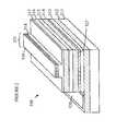
- FIG. 1is a perspective view of an edge-emitting semiconductor laser 10 .
- FIG. 2is a prospective view of a laser 350 according to one embodiment of the present invention.
- FIG. 3is a cross-sectional view of the optical semiconductor device 50 according to another embodiment of the present invention.
- FIG. 1is a perspective view of an edge-emitting semiconductor laser 10 .
- Laser 10is an example of a specific laser geometry that facilitates low threshold and single lateral mode operation.
- Laser 10is constructed on a substrate 11 by growing a number of epitaxial layers on substrate 11 .
- the n-type layersare typically constructed first.
- the first layeris the n-contact layer 12 followed by an n-cladding layer 13 .
- the active layerconsisting of a guide layer 14 , the light generation layer 15 , and a second guide layer 16 are then deposited.
- a p-cladding layer 17 and a p-contact layer 18are then deposited on the p-guiding layer 16 .
- a metallic electrode layer 19is deposited on the p-contact layer to provide one of the electrical connections.
- the layered stackis then etched to form the ridge structure shown at 21 and to expose the n-contact layer on which metallic electrode 20 is deposited. The light is confined to region 22 by the cladding layers and ridge structure.
- OMPVE growth kineticsthe growth along the wurtzite c-axis occurs with the so-called gallium-face exposed at the surface.
- This crystal orientationfixes the orientation of the polarization fields at any InGaN/GaN quantum wells in the structure. In all devices reported to date, these fields have been opposed to the built-in field of the pn junction, whose direction is fixed by the n-layer always being grown first.
- the present inventionis based on the observation that this relative orientation between the pn junction and the intense heterostructure polarization field in the InGaN wells is deleterious, and that the resultant reduction in efficiency is large.
- This fielddepletes electrons from the n-side of the InGaN wells, depletes holes from the p-side of the InGaN wells, and reduces the pn product in the wells, which dramatically reduces the desired radiative recombination.
- the devicescan be constructed with a p-down light-emitting junction.
- the n-layeris always grown first, and the n-type GaN provides current spreading under the device.
- the lateral conductivity of p-type GaNis generally too low for this purpose.
- the commonly used p-type dopant (Mg)will spread into the upper regions of the structure during subsequent processing steps if it is introduced in the lower regions making its profile difficult to control.
- the p-dopantcauses surface roughening and other degradation that reduces the quality of material in layers located above the p-doped region. For all of these reasons, workers in the field have always avoided a p-down structure.
- FIG. 2is a prospective view of a first embodiment of a laser 350 according to the present invention.
- Laser 350utilizes a reverse bias tunnel diode to enable an upside-down arrangement in which the polarization field points in the proper direction to provide increased current confinement.
- Laser 350is constructed by depositing an n-contact layer 312 on a sapphire substrate 311 .
- An n-cladding layer 313is then deposited on n-contact layer 312 and a p-cladding layer 327 is deposited on n-cladding layer 313 .
- the reverse-biased tunnel diode junctionis located at the interface of layers 327 and 313 in this embodiment of the present invention.
- the construction of such reversed-bias tunneling diodesis discussed in detail in U.S. patent application Ser. No.: 09/586,406, which is hereby incorporated by reference, and hence, will not be discussed in detail here.
- the active regionconsisting of p-guide layer 314 , active layer 315 , and n-guide layer 316 is then deposited.
- a second n-cladding layer 317 and a second n-contact layer 318are then deposited.
- the layered stackis then etched to provide ridge region 321 on which an n-electrode 319 is deposited.
- the second electrical contact 320is deposited on the first n-contact layer after the stack is etched back to expose layer 312 .
- Electrode 320is also an n-electrode. Since the resistivity of the n-contact layer 312 is much lower than that of the p-contact layer used in a conventional laser, the current spreading problems associated with a conventional upside-down laser are eliminated.
- LEDswhich are similar in layer structure but without the AlGaN cladding layers.
- the better carrier confinement obtained with the polarization field reversed relative to the direction of carrier flowresults in less carrier overflow, and hence, increased quantum efficiency at higher current density. This results in a considerable cost advantage by increasing the amount of light flux emitted per unit chip area.
- the reverse bias tunnel diodecan be placed anywhere between the active region and the n-contact.
- the second method for reversing the direction of the polarization fieldutilizes a GaN starting layer that has a reversed c-axis, i.e., with the nitrogen-face exposed.
- the term “reversed c-axis substrate”refers to a substrate with the nitrogen-face exposed. If bulk GaN substrate is available, the nitrogen-face of the bulk GaN 0001 substrate may be utilized. In the absence of such substrates, a GaN layer is grown on a sapphire substrate with the conventional c-axis orientation. The layer is then removed from the original substrate, turned over to provide a starting layer having the nitrogen-face exposed and affixed to an appropriate substrate or carrier to provide support during the subsequent processing. The laser or LED is then constructed in the conventional manner on this reversed c-axis n-doped layer to provide a structure that is similar to that shown in FIG. 1, except for the crystal-orientation of the material in the GaN layer 12 .
- This embodiment of the present inventionis based on the observation that the GaN at the GaN/sapphire interface can be decomposed by exposing the GaN at the interface to UV light in the range of power densities of 5-20 megawatts/cm 2 at a wavelength of 248 nm.
- the GaNis opaque to UV at this wavelength.
- Sapphireon the other hand, is transparent to UV light with a wavelength of 248 nm.
- UV light directed at the GaN/sapphire interface through the sapphire substrateheats the layer of material at the interface.
- the GaNis heated to a temperature at which it decomposes the GaN into Ga and N.
- This procedurehas been used to separate GaN thin films from sapphire (W. Wong, T. Sands; 10 th Conference on Semiconductor and Insulating Materials, June 1998, Berkeley, Calif., paper Th2.2). This technique, of course, assumes that the GaN layer is sufficiently thick to be self-supporting.
- the reversed c-axis starting layer discussed aboveis obtained by growing a “seed layer” with the reversed c-axis by a technique such as MBE.
- the “conventional” device structureis then grown on this “polarization-reversed substrate”. Again, the doping can now be p on top and n on the bottom and still provide the correct orientation of the polarization field.
- Methods for growing such inverted structuresare known to the art. The reader is directed to M. J. Murphy, et al, “Molecular beam epitaxial growth of normal and inverted two-dimensional electron gases in AlGan/GaN based heterostructures”, J. Vac. Sci. Technol. B., 17(3), May-June 1999, which is hereby incorporated by reference.
- a different crystal orientation in which the polarization field is in the proper orientationis provided by selectively etching or growing a surface on a conventional device to provide a growth surface on a crystal face having the proper orientation.
- FIG. 3is a cross-sectional view of the optical semiconductor device 50 according to another embodiment of the present invention in which only the layers related solely to light emission and absorption have the desired facet orientation.
- Device 50is constructed by growing an n-type GaN contact layer 53 and an ntype AlGaN cladding layer 54 on the ⁇ 0001 ⁇ plane orientation on the substrate 51 such as SiC or GaN based on conventional technology. Next, by selective growing or selective etching, a new plane is exposed or formed. The GaInN/GaN or GaInN/GaInN strained multiple quantum well layer 55 is then formed by repeating the crystal growth on this new plane.
- the remaining p-type AlGaN cladding layer 56 and the p-type GaN contact layer 57are successively deposited and formed.
- the p-type AlGaN cladding layer 56 and the p-type GaN contact layer 57change the crystal structure back to that corresponding to the ⁇ 0001 ⁇ plane from the facet orientation of the well layer 55 and become layers with specific thicknesses.
- the n-electrode 58 and the p-electrode 59are formed as the electrodes on the n-type GaN contact layer 53 and the p-type GaN contact layer 57 , respectively.
- the growing surfaces 55 A, 55 B on both sides of the GaInN strained multiple quantum well layer 55are the desired plane, i.e., the plane for which the polarization has the desired orientation.
- the p-type AlGaN cladding layer 56 and the p-type GaN contact layer 57become flat growing surfaces. To simplify the next process, it is advisable that they be several microns thick.
- an AlN buffer layer 52is grown on the substrate 51 .
- the present inventionhas been described in terms of GaN devices, it will be obvious to those skilled in the art from the preceding discussion that the invention is applicable to any material system in which polarization fields (or polarization charges) appear when heterostructures are fabricated.
- the present inventionis applicable to any heterostructure device, which incorporates a pn junction, or a metal-semiconductor junction, with a built-in field. Examples of such devices include LEDs, resonant cavity LEDs, edge-emitting lasers, and VCSELs.
Landscapes
- Physics & Mathematics (AREA)
- Condensed Matter Physics & Semiconductors (AREA)
- General Physics & Mathematics (AREA)
- Electromagnetism (AREA)
- Optics & Photonics (AREA)
- Semiconductor Lasers (AREA)
- Led Devices (AREA)
Abstract
Description
- This is a continuation-in-part of U.S. patent application Ser. No. 09/586,406 filed Jun. 2, 2000.[0001]
- The present invention relates to semiconductor lasers and light emitting diodes, and more particularly, to an improved device architecture that increases the efficiency of such devices.[0002]
- The development of short wavelength light emitting devices is of great interest in the semiconductor arts. Such short wavelength devices hold the promise of providing increased storage density for optical disks as well as full-color displays and white light sources when used in conjunction with devices that emit light at longer wavelengths. For example, blue lasers are expected to increase the storage density of optical disks by a factor of three.[0003]
- One promising class of short wavelength light emitting devices is based on group III-V semiconductors, particularly group III nitride semiconductors. As used herein, the class of group III nitride semiconductors includes GaN, AlN, InN, BN, and alloys thereof, such as GaInN, AlGaN, and AlGaInN. To simplify the following discussion, “GaN semiconductors” includes GaN, and group III nitride semiconductors whose primary component is the GaN as in GaInN, AlGaN, AlGaInN.[0004]
- Light emitting diodes (LEDs) and semiconductor laser diodes are fabricated on epitaxially grown layers of GaN and related alloys of semiconductor materials including an active layer that generates light by recombining holes and electrons. The active layer is sandwiched between p-type and n-type contacts to form a p-n or n-p diode structure. A p-electrode and an n-electrode are used to connect the p-contact and n-contact, respectively, to the power source used to drive the device. The overall efficiency of the device may be defined to be the light emitted to the outside per watt of drive power. To maximize the light efficiency, both the light generated per watt of drive power in the active layer and the amount of light exiting from the device in a useful direction must be considered.[0005]
- GaN based LEDs and laser diodes (LDs) are fabricated by epitaxy techniques where the LED or LD layer structure is grown “p-up” on top of a relatively thick n-type GaN (or AlGaN) buffer layer which is typically grown on a sapphire or SiC substrate. The individual devices are then defined by a mesa etch through the p-n junction. The anode or p-type contact metal is applied to the top of the mesa and the specific resistance of the Schottky contact is minimized by the use of a large work-function metal such as Ni or Pd and by the use of very high p-type doping in the topmost regions of the p-type layers. For the conductive n-type SiC substrate, the cathode is a large-area ohmic contact formed by metallizing the substrate back surface. In the case of the non-conducting sapphire substrate, the cathode or n-type contact metal is applied in the field close to the mesa edge to provide a lateral current flow through the thick n-type buffer layer to the p-n junction within the mesa.[0006]
- There are several drawbacks to this conventional design. First, p-type GaN is very resistive compared to other common semiconductors even when grown under optimized conditions. As a result, there is virtually no lateral current spreading in p-type GaN. To overcome this lack of current spreading, conventional p-up LEDs require a semi-transparent metal electrode that covers the p-contact to provide the lateral current spreading. This electrode reduces that amount of light that leaves the device, and hence, reduces the efficiency. In p-type AlGaN, the resistivity is even higher, increasing with increasing Al mole-fraction. Thus the p-type AlGaN layer in laser diodes used for optical wave-guiding causes further resistive heating that degrades laser performance.[0007]
- Secondly, the III-V materials, in their wurtzite or hexagonal crystalline form, exhibit large spontaneous polarization charges at heterointerfaces and strong piezoelectric effects at lattice mismatched heterointerfaces, especially when grown along the [0001] crystal orientation or c-axis as is usually the case. The direction of the resulting polarization field is such that it adversely affects the optical recombination rate in a conventional p-up device.[0008]
- All prior nitride-based pn junctions, which have been created for purposes of efficient light emission, have been grown by OMVPE, and include InGaN quantum wells which concentrate the electrons and holes together to achieve a large pn product and efficient radiative recombination. As a consequence of OMVPE growth kinetics, the growth along the wurtzite c-axis occurs with the so-called gallium-face exposed at the surface. This crystal orientation fixes the orientation of the polarization fields at any InGaN/GaN quantum wells in the structure. In all devices reported to date, these fields have been opposed to the built-in field of the pn junction, whose direction is fixed by the n-layer always being grown first.[0009]
- Broadly, it is the object of the present invention to provide improved LEDs and semiconductor lasers based on group III-V semiconductors.[0010]
- It is a further object of the present invention to provide light emitting devices with increased light output efficiency.[0011]
- These and other objects of the present invention will become apparent to those skilled in the art from the following detailed description of the invention and the accompanying drawings.[0012]
- The present invention is an optical semiconductor device and method of making the same in which the device has an active layer for generating light via the recombination of holes and electrons therein. The active layer includes a plurality of semiconductor layers including an n-p junction between an n-type layer and a p-type layer. The active layer has a polarization field therein having a field direction that depends on the orientation of the active layer when the active layer is grown. In the present invention, the polarization field in the active layer has an orientation such that the polarization field is directed from the n-layer to the p-layer. Including a reverse bias tunnel diode in the optical device can provide the desired field orientation. In other embodiments, the field orientation is achieved by growing the active layer on a substrate that induces growth in a manner that provides the desired field direction. In one embodiment, the device is grown on a substrate having a crystalline axis at an angle to the Ga- and N- faces of GaN-based layer.[0013]
- FIG. 1 is a perspective view of an edge-emitting[0014]
semiconductor laser 10. - FIG. 2 is a prospective view of a[0015]
laser 350 according to one embodiment of the present invention. - FIG. 3 is a cross-sectional view of the[0016]
optical semiconductor device 50 according to another embodiment of the present invention - The manner in which the present invention provides its advantages may be more easily understood with reference to FIG. 1, which is a perspective view of an edge-emitting[0017]
semiconductor laser 10.Laser 10 is an example of a specific laser geometry that facilitates low threshold and single lateral mode operation.Laser 10 is constructed on a substrate11 by growing a number of epitaxial layers on substrate11. For GaN lasers, the n-type layers are typically constructed first. The first layer is the n-contact layer 12 followed by an n-claddinglayer 13. The active layer consisting of aguide layer 14, the light generation layer15, and asecond guide layer 16 are then deposited. A p-cladding layer 17 and a p-contact layer 18 are then deposited on the p-guidinglayer 16. Ametallic electrode layer 19 is deposited on the p-contact layer to provide one of the electrical connections. The layered stack is then etched to form the ridge structure shown at21 and to expose the n-contact layer on whichmetallic electrode 20 is deposited. The light is confined toregion 22 by the cladding layers and ridge structure. - Prior-art nitride-based pn junctions that have been created for purposes of efficient light emission, have been grown by OMVPE, and include InGaN quantum wells that concentrate the electrons and holes together to achieve a large p-n product and efficient radiative recombination. As a consequence of OMPVE growth kinetics, the growth along the wurtzite c-axis occurs with the so-called gallium-face exposed at the surface. This crystal orientation fixes the orientation of the polarization fields at any InGaN/GaN quantum wells in the structure. In all devices reported to date, these fields have been opposed to the built-in field of the pn junction, whose direction is fixed by the n-layer always being grown first.[0018]
- The present invention is based on the observation that this relative orientation between the pn junction and the intense heterostructure polarization field in the InGaN wells is deleterious, and that the resultant reduction in efficiency is large. This field depletes electrons from the n-side of the InGaN wells, depletes holes from the p-side of the InGaN wells, and reduces the pn product in the wells, which dramatically reduces the desired radiative recombination.[0019]
- If the orientation of this heterostructure polarization field were reversed, the pn product in the wells is increased, with a resultant increase in device efficiency. In addition, the penetration of both carriers beyond the well is drastically reduced. This increased carrier confinement also improves the device efficiency.[0020]
- There are many ways of realizing the performance advantage that results from reversing the direction of carrier transport relative to the polarization field. First, the devices can be constructed with a p-down light-emitting junction. In a conventional GaNpn junction light-emitting device, the n-layer is always grown first, and the n-type GaN provides current spreading under the device. The lateral conductivity of p-type GaN is generally too low for this purpose. In addition, the commonly used p-type dopant (Mg) will spread into the upper regions of the structure during subsequent processing steps if it is introduced in the lower regions making its profile difficult to control. Further, the p-dopant causes surface roughening and other degradation that reduces the quality of material in layers located above the p-doped region. For all of these reasons, workers in the field have always avoided a p-down structure.[0021]
- In this embodiment of the present invention, these problems are overcome by growing a heavily-doped p++/n++ junction on an n-type current spreading layer. This method has the additional advantage of providing n-type layers for current spreading on both sides of the junction, and hence, avoids the current spreading problems of prior art devices.[0022]
- Refer now to FIG. 2, which is a prospective view of a first embodiment of a[0023]
laser 350 according to the present invention.Laser 350 utilizes a reverse bias tunnel diode to enable an upside-down arrangement in which the polarization field points in the proper direction to provide increased current confinement.Laser 350 is constructed by depositing an n-contact layer 312 on asapphire substrate 311. An n-cladding layer 313 is then deposited on n-contact layer 312 and a p-cladding layer 327 is deposited on n-cladding layer 313. The reverse-biased tunnel diode junction is located at the interface oflayers - The active region consisting of p-[0024]
guide layer 314,active layer 315, and n-guide layer 316 is then deposited. A second n-cladding layer 317 and a second n-contact layer 318 are then deposited. The layered stack is then etched to provideridge region 321 on which an n-electrode 319 is deposited. The secondelectrical contact 320 is deposited on the first n-contact layer after the stack is etched back to exposelayer 312.Electrode 320 is also an n-electrode. Since the resistivity of the n-contact layer 312 is much lower than that of the p-contact layer used in a conventional laser, the current spreading problems associated with a conventional upside-down laser are eliminated. This also applies to LEDs, which are similar in layer structure but without the AlGaN cladding layers. In the case of LEDs, the better carrier confinement obtained with the polarization field reversed relative to the direction of carrier flow, results in less carrier overflow, and hence, increased quantum efficiency at higher current density. This results in a considerable cost advantage by increasing the amount of light flux emitted per unit chip area. - While the discussion of[0025]
laser 350 utilized a specific location for the reverse bias tunnel diode, it will be obvious to those skilled in the art from the preceding discussion that other locations can be utilized without deviating from the teachings of the present invention. For example, the reverse bias tunnel diode can be placed anywhere between the active region and the n-contact. - The second method for reversing the direction of the polarization field utilizes a GaN starting layer that has a reversed c-axis, i.e., with the nitrogen-face exposed. In the following discussion, the term “reversed c-axis substrate” refers to a substrate with the nitrogen-face exposed. If bulk GaN substrate is available, the nitrogen-face of the bulk GaN 0001 substrate may be utilized. In the absence of such substrates, a GaN layer is grown on a sapphire substrate with the conventional c-axis orientation. The layer is then removed from the original substrate, turned over to provide a starting layer having the nitrogen-face exposed and affixed to an appropriate substrate or carrier to provide support during the subsequent processing. The laser or LED is then constructed in the conventional manner on this reversed c-axis n-doped layer to provide a structure that is similar to that shown in FIG. 1, except for the crystal-orientation of the material in the[0026]
GaN layer 12. - This embodiment of the present invention is based on the observation that the GaN at the GaN/sapphire interface can be decomposed by exposing the GaN at the interface to UV light in the range of power densities of 5-20 megawatts/cm[0027]2at a wavelength of 248 nm. The GaN is opaque to UV at this wavelength. Sapphire, on the other hand, is transparent to UV light with a wavelength of 248 nm. Hence, UV light directed at the GaN/sapphire interface through the sapphire substrate heats the layer of material at the interface. The GaN is heated to a temperature at which it decomposes the GaN into Ga and N. This procedure has been used to separate GaN thin films from sapphire (W. Wong, T. Sands; 10thConference on Semiconductor and Insulating Materials, June 1998, Berkeley, Calif., paper Th2.2). This technique, of course, assumes that the GaN layer is sufficiently thick to be self-supporting.
- In a third embodiment of the present invention, the reversed c-axis starting layer discussed above is obtained by growing a “seed layer” with the reversed c-axis by a technique such as MBE. The “conventional” device structure is then grown on this “polarization-reversed substrate”. Again, the doping can now be p on top and n on the bottom and still provide the correct orientation of the polarization field. Methods for growing such inverted structures are known to the art. The reader is directed to M. J. Murphy, et al, “Molecular beam epitaxial growth of normal and inverted two-dimensional electron gases in AlGan/GaN based heterostructures”, J. Vac. Sci. Technol. B., 17(3), May-June 1999, which is hereby incorporated by reference.[0028]
- In a fourth embodiment of the present invention, a different crystal orientation in which the polarization field is in the proper orientation is provided by selectively etching or growing a surface on a conventional device to provide a growth surface on a crystal face having the proper orientation. Refer now to FIG. 3, which is a cross-sectional view of the[0029]
optical semiconductor device 50 according to another embodiment of the present invention in which only the layers related solely to light emission and absorption have the desired facet orientation.Device 50 is constructed by growing an n-typeGaN contact layer 53 and an ntypeAlGaN cladding layer 54 on the {0001} plane orientation on thesubstrate 51 such as SiC or GaN based on conventional technology. Next, by selective growing or selective etching, a new plane is exposed or formed. The GaInN/GaN or GaInN/GaInN strained multiplequantum well layer 55 is then formed by repeating the crystal growth on this new plane. - Next, the remaining p-type[0030]
AlGaN cladding layer 56 and the p-typeGaN contact layer 57 are successively deposited and formed. The p-typeAlGaN cladding layer 56 and the p-typeGaN contact layer 57 change the crystal structure back to that corresponding to the {0001 } plane from the facet orientation of thewell layer 55 and become layers with specific thicknesses. The n-electrode 58 and the p-electrode 59 are formed as the electrodes on the n-typeGaN contact layer 53 and the p-typeGaN contact layer 57, respectively. The growing surfaces55A,55B on both sides of the GaInN strained multiplequantum well layer 55 are the desired plane, i.e., the plane for which the polarization has the desired orientation. The p-typeAlGaN cladding layer 56 and the p-typeGaN contact layer 57 become flat growing surfaces. To simplify the next process, it is advisable that they be several microns thick. In the preferred embodiment of the present invention, anAlN buffer layer 52 is grown on thesubstrate 51. - While the present invention has been described in terms of GaN devices, it will be obvious to those skilled in the art from the preceding discussion that the invention is applicable to any material system in which polarization fields (or polarization charges) appear when heterostructures are fabricated. For example, the present invention is applicable to any heterostructure device, which incorporates a pn junction, or a metal-semiconductor junction, with a built-in field. Examples of such devices include LEDs, resonant cavity LEDs, edge-emitting lasers, and VCSELs.[0031]
- Various modifications to the present invention will become apparent to those skilled in the art from the foregoing description and accompanying drawings. Accordingly, the present invention is to be limited solely by the scope of the following claims.[0032]
Claims (11)
Priority Applications (1)
| Application Number | Priority Date | Filing Date | Title |
|---|---|---|---|
| US10/026,232US6853663B2 (en) | 2000-06-02 | 2001-12-21 | Efficiency GaN-based light emitting devices |
Applications Claiming Priority (2)
| Application Number | Priority Date | Filing Date | Title |
|---|---|---|---|
| US09/586,406US6526082B1 (en) | 2000-06-02 | 2000-06-02 | P-contact for GaN-based semiconductors utilizing a reverse-biased tunnel junction |
| US10/026,232US6853663B2 (en) | 2000-06-02 | 2001-12-21 | Efficiency GaN-based light emitting devices |
Related Parent Applications (1)
| Application Number | Title | Priority Date | Filing Date |
|---|---|---|---|
| US09/586,406Continuation-In-PartUS6526082B1 (en) | 2000-06-02 | 2000-06-02 | P-contact for GaN-based semiconductors utilizing a reverse-biased tunnel junction |
Publications (2)
| Publication Number | Publication Date |
|---|---|
| US20020110172A1true US20020110172A1 (en) | 2002-08-15 |
| US6853663B2 US6853663B2 (en) | 2005-02-08 |
Family
ID=46278615
Family Applications (1)
| Application Number | Title | Priority Date | Filing Date |
|---|---|---|---|
| US10/026,232Expired - LifetimeUS6853663B2 (en) | 2000-06-02 | 2001-12-21 | Efficiency GaN-based light emitting devices |
Country Status (1)
| Country | Link |
|---|---|
| US (1) | US6853663B2 (en) |
Cited By (40)
| Publication number | Priority date | Publication date | Assignee | Title |
|---|---|---|---|---|
| US20040206962A1 (en)* | 2003-04-15 | 2004-10-21 | Erchak Alexei A. | Light emitting devices |
| US20040206971A1 (en)* | 2003-04-15 | 2004-10-21 | Erchak Alexei A. | Light emitting devices |
| US20040207319A1 (en)* | 2003-04-15 | 2004-10-21 | Erchak Alexei A. | Light emitting devices |
| US20040207320A1 (en)* | 2003-04-15 | 2004-10-21 | Erchak Alexei A. | Light emitting devices |
| US20040207310A1 (en)* | 2003-04-15 | 2004-10-21 | Erchak Alexei A. | Light emitting devices |
| US20040207323A1 (en)* | 2003-04-15 | 2004-10-21 | Erchak Alexei A. | Light emitting devices |
| US20040259279A1 (en)* | 2003-04-15 | 2004-12-23 | Erchak Alexei A. | Light emitting device methods |
| US20040259285A1 (en)* | 2003-04-15 | 2004-12-23 | Erchak Alexei A. | Light emitting device methods |
| US20050040424A1 (en)* | 2003-04-15 | 2005-02-24 | Erchak Alexei A. | Light emitting diode systems |
| US20050051785A1 (en)* | 2003-04-15 | 2005-03-10 | Erchak Alexei A. | Electronic device contact structures |
| US20050059179A1 (en)* | 2003-09-17 | 2005-03-17 | Erchak Alexei A. | Light emitting device processes |
| US20050059178A1 (en)* | 2003-09-17 | 2005-03-17 | Erchak Alexei A. | Light emitting device processes |
| US20050087757A1 (en)* | 2003-04-15 | 2005-04-28 | Luminus Devices, Inc., A Delaware Corporation | Light emitting devices |
| US20050087754A1 (en)* | 2003-04-15 | 2005-04-28 | Erchak Alexei A. | Light emitting systems |
| US20050127375A1 (en)* | 2003-12-12 | 2005-06-16 | Erchak Alexei A. | Optical display systems and methods |
| US20050180475A1 (en)* | 2004-02-18 | 2005-08-18 | Samsung Electronics Co., Ltd. | Semiconductor laser device |
| US20050205884A1 (en)* | 2004-03-19 | 2005-09-22 | Lumileds Lighting U.S., Llc | Semiconductor light emitting devices including in-plane light emitting layers |
| US20050224826A1 (en)* | 2004-03-19 | 2005-10-13 | Lumileds Lighting, U.S., Llc | Optical system for light emitting diodes |
| US20050286586A1 (en)* | 2004-06-25 | 2005-12-29 | Finisar Corporation | Geometric optimizations for reducing spontaneous emissions in photodiodes |
| US20050286593A1 (en)* | 2004-06-25 | 2005-12-29 | James Guenter | Light emitting device with an integrated monitor photodiode |
| US20060038188A1 (en)* | 2004-08-20 | 2006-02-23 | Erchak Alexei A | Light emitting diode systems |
| US20060043391A1 (en)* | 2003-04-15 | 2006-03-02 | Erchak Alexei A | Light emitting devices for liquid crystal displays |
| US20060146904A1 (en)* | 2004-12-30 | 2006-07-06 | Finisar Corporation | Integrated light emitting device and photodiode with ohmic contact |
| US20060163590A1 (en)* | 2005-01-21 | 2006-07-27 | Erchak Alexei A | Packaging designs for LEDs |
| WO2006087684A1 (en) | 2005-02-18 | 2006-08-24 | Koninklijke Philips Electronics N.V. | Reverse polarization light emitting region for a nitride light emitting device |
| US20060202215A1 (en)* | 2005-03-14 | 2006-09-14 | Lumileds Lighting U.S., Llc | Polarization-reversed III-nitride light emitting device |
| US7170100B2 (en) | 2005-01-21 | 2007-01-30 | Luminus Devices, Inc. | Packaging designs for LEDs |
| US20070045640A1 (en)* | 2005-08-23 | 2007-03-01 | Erchak Alexei A | Light emitting devices for liquid crystal displays |
| US20080099777A1 (en)* | 2005-10-19 | 2008-05-01 | Luminus Devices, Inc. | Light-emitting devices and related systems |
| CN100391014C (en)* | 2003-08-04 | 2008-05-28 | 三星电子株式会社 | Semiconductor device with superlattice semiconductor layer and manufacturing method thereof |
| US20080274574A1 (en)* | 2007-03-20 | 2008-11-06 | Luminus Devices, Inc. | Laser liftoff structure and related methods |
| US20090023239A1 (en)* | 2004-07-22 | 2009-01-22 | Luminus Devices, Inc. | Light emitting device processes |
| US20110027973A1 (en)* | 2009-07-31 | 2011-02-03 | Applied Materials, Inc. | Method of forming led structures |
| KR101241533B1 (en) | 2004-09-22 | 2013-03-08 | 엘지이노텍 주식회사 | Light emitting diode and method for manufacturing led |
| TWI392106B (en)* | 2004-01-30 | 2013-04-01 | Philips Lumileds Lighting Co | Group III nitride light-emitting device with reduced polarization field |
| US20130207076A1 (en)* | 2010-09-08 | 2013-08-15 | Sumitomo Electric Industries ,Ltd. | Method for fabricating group iii nitride semiconductor light emitting device, and group iii nitride semiconductor light emitting device |
| US9396941B2 (en)* | 2010-09-17 | 2016-07-19 | The United States Of America, As Represented By The Secretary Of The Navy | Method for vertical and lateral control of III-N polarity |
| US20180012753A1 (en)* | 2015-01-21 | 2018-01-11 | Centre National De La Recherche Scientifique (Cnrs) | Method for producing a passivated semiconductor structure based on group iii nitrides, and one such structure |
| JP2020505762A (en)* | 2017-01-12 | 2020-02-20 | 中国科学院蘇州納米技術与納米▲ファン▼生研究所 | Nitride semiconductor light emitting device and method of manufacturing the same |
| US10608404B2 (en) | 2017-02-14 | 2020-03-31 | Cisco Technology, Inc. | Bonded laser with solder-free laser active stripe in facing relationship with submount |
Families Citing this family (4)
| Publication number | Priority date | Publication date | Assignee | Title |
|---|---|---|---|---|
| KR100506739B1 (en)* | 2003-12-23 | 2005-08-08 | 삼성전기주식회사 | Growth method of aluminum-containing nitride semiconductor single crystal |
| US7341878B2 (en)* | 2005-03-14 | 2008-03-11 | Philips Lumileds Lighting Company, Llc | Wavelength-converted semiconductor light emitting device |
| WO2008070088A2 (en)* | 2006-12-05 | 2008-06-12 | Nano Terra Inc. | Edge-emitting light-emitting diode arrays and methods of making and using the same |
| US20110233521A1 (en)* | 2010-03-24 | 2011-09-29 | Cree, Inc. | Semiconductor with contoured structure |
Citations (14)
| Publication number | Priority date | Publication date | Assignee | Title |
|---|---|---|---|---|
| US5070510A (en)* | 1989-12-12 | 1991-12-03 | Sharp Kabushiki Kaisha | Semiconductor laser device |
| US5079774A (en)* | 1990-12-27 | 1992-01-07 | International Business Machines Corporation | Polarization-tunable optoelectronic devices |
| US5331654A (en)* | 1993-03-05 | 1994-07-19 | Photonics Research Incorporated | Polarized surface-emitting laser |
| US5383211A (en)* | 1993-11-02 | 1995-01-17 | Xerox Corporation | TM-polarized laser emitter using III-V alloy with nitrogen |
| US5530267A (en)* | 1995-03-14 | 1996-06-25 | At&T Corp. | Article comprising heteroepitaxial III-V nitride semiconductor material on a substrate |
| US5693965A (en)* | 1995-11-02 | 1997-12-02 | Nec Corporation | Laser diode having narrowed radiation angle characteristic |
| US5779027A (en)* | 1996-02-14 | 1998-07-14 | Rexnord Corporation | Sideflexing conveyor including lubrication inserts |
| US5892784A (en)* | 1994-10-27 | 1999-04-06 | Hewlett-Packard Company | N-drive p-common surface emitting laser fabricated on n+ substrate |
| US5953362A (en)* | 1997-12-15 | 1999-09-14 | Pamulapati; Jagadeesh | Strain induce control of polarization states in vertical cavity surface emitting lasers and method of making same |
| US6100546A (en)* | 1994-04-07 | 2000-08-08 | Sdl, Inc. | III-V arsenide-nitride semiconductor |
| US6294440B1 (en)* | 1998-04-10 | 2001-09-25 | Sharp Kabushiki Kaisha | Semiconductor substrate, light-emitting device, and method for producing the same |
| US6369403B1 (en)* | 1999-05-27 | 2002-04-09 | The Board Of Trustees Of The University Of Illinois | Semiconductor devices and methods with tunnel contact hole sources and non-continuous barrier layer |
| US6501154B2 (en)* | 1997-06-03 | 2002-12-31 | Sony Corporation | Semiconductor substrate made of a nitride III-V compound semiconductor having a wurtzite-structured crystal structure |
| US6515313B1 (en)* | 1999-12-02 | 2003-02-04 | Cree Lighting Company | High efficiency light emitters with reduced polarization-induced charges |
- 2001
- 2001-12-21USUS10/026,232patent/US6853663B2/ennot_activeExpired - Lifetime
Patent Citations (14)
| Publication number | Priority date | Publication date | Assignee | Title |
|---|---|---|---|---|
| US5070510A (en)* | 1989-12-12 | 1991-12-03 | Sharp Kabushiki Kaisha | Semiconductor laser device |
| US5079774A (en)* | 1990-12-27 | 1992-01-07 | International Business Machines Corporation | Polarization-tunable optoelectronic devices |
| US5331654A (en)* | 1993-03-05 | 1994-07-19 | Photonics Research Incorporated | Polarized surface-emitting laser |
| US5383211A (en)* | 1993-11-02 | 1995-01-17 | Xerox Corporation | TM-polarized laser emitter using III-V alloy with nitrogen |
| US6100546A (en)* | 1994-04-07 | 2000-08-08 | Sdl, Inc. | III-V arsenide-nitride semiconductor |
| US5892784A (en)* | 1994-10-27 | 1999-04-06 | Hewlett-Packard Company | N-drive p-common surface emitting laser fabricated on n+ substrate |
| US5530267A (en)* | 1995-03-14 | 1996-06-25 | At&T Corp. | Article comprising heteroepitaxial III-V nitride semiconductor material on a substrate |
| US5693965A (en)* | 1995-11-02 | 1997-12-02 | Nec Corporation | Laser diode having narrowed radiation angle characteristic |
| US5779027A (en)* | 1996-02-14 | 1998-07-14 | Rexnord Corporation | Sideflexing conveyor including lubrication inserts |
| US6501154B2 (en)* | 1997-06-03 | 2002-12-31 | Sony Corporation | Semiconductor substrate made of a nitride III-V compound semiconductor having a wurtzite-structured crystal structure |
| US5953362A (en)* | 1997-12-15 | 1999-09-14 | Pamulapati; Jagadeesh | Strain induce control of polarization states in vertical cavity surface emitting lasers and method of making same |
| US6294440B1 (en)* | 1998-04-10 | 2001-09-25 | Sharp Kabushiki Kaisha | Semiconductor substrate, light-emitting device, and method for producing the same |
| US6369403B1 (en)* | 1999-05-27 | 2002-04-09 | The Board Of Trustees Of The University Of Illinois | Semiconductor devices and methods with tunnel contact hole sources and non-continuous barrier layer |
| US6515313B1 (en)* | 1999-12-02 | 2003-02-04 | Cree Lighting Company | High efficiency light emitters with reduced polarization-induced charges |
Cited By (122)
| Publication number | Priority date | Publication date | Assignee | Title |
|---|---|---|---|---|
| US8513692B2 (en) | 2003-04-15 | 2013-08-20 | Luminus Devices, Inc. | Light emitting devices |
| US7074631B2 (en) | 2003-04-15 | 2006-07-11 | Luminus Devices, Inc. | Light emitting device methods |
| US20040207319A1 (en)* | 2003-04-15 | 2004-10-21 | Erchak Alexei A. | Light emitting devices |
| US20040207320A1 (en)* | 2003-04-15 | 2004-10-21 | Erchak Alexei A. | Light emitting devices |
| US20040207310A1 (en)* | 2003-04-15 | 2004-10-21 | Erchak Alexei A. | Light emitting devices |
| US20040207323A1 (en)* | 2003-04-15 | 2004-10-21 | Erchak Alexei A. | Light emitting devices |
| US20040259279A1 (en)* | 2003-04-15 | 2004-12-23 | Erchak Alexei A. | Light emitting device methods |
| US20040259285A1 (en)* | 2003-04-15 | 2004-12-23 | Erchak Alexei A. | Light emitting device methods |
| US20050040419A1 (en)* | 2003-04-15 | 2005-02-24 | Luminus Devices, Inc., A Delaware Corporation | Light emitting devices |
| US20050040424A1 (en)* | 2003-04-15 | 2005-02-24 | Erchak Alexei A. | Light emitting diode systems |
| US20050051785A1 (en)* | 2003-04-15 | 2005-03-10 | Erchak Alexei A. | Electronic device contact structures |
| US20050051787A1 (en)* | 2003-04-15 | 2005-03-10 | Luminus Devices, Inc., A Delaware Corporation | Light emitting devices |
| US7521854B2 (en) | 2003-04-15 | 2009-04-21 | Luminus Devices, Inc. | Patterned light emitting devices and extraction efficiencies related to the same |
| US7521273B2 (en) | 2003-04-15 | 2009-04-21 | Luminus Devices, Inc. | Light emitting device methods |
| WO2004093142A3 (en)* | 2003-04-15 | 2005-04-14 | Luminus Devices Inc | Light emitting device methods |
| US20060141648A1 (en)* | 2003-04-15 | 2006-06-29 | Luminus Devices, Inc., A Delaware Corporation | Light emitting device methods |
| US20050087754A1 (en)* | 2003-04-15 | 2005-04-28 | Erchak Alexei A. | Light emitting systems |
| US7504669B2 (en) | 2003-04-15 | 2009-03-17 | Luminus Devices, Inc. | Light emitting devices |
| US20050145877A1 (en)* | 2003-04-15 | 2005-07-07 | Luminus Devices, Inc. A Delaware Corporation | Light emitting devices |
| US20050151125A1 (en)* | 2003-04-15 | 2005-07-14 | Luminus Device Inc., A Delaware Corporation | Light emitting devices |
| US20050167687A1 (en)* | 2003-04-15 | 2005-08-04 | Luminus Devices, Inc. | Light emitting devices |
| US7495260B2 (en) | 2003-04-15 | 2009-02-24 | Luminus Devices, Inc. | Light emitting devices |
| US7482640B2 (en) | 2003-04-15 | 2009-01-27 | Luminus Devices, Inc. | Electronic device contact structures |
| US20050208689A1 (en)* | 2003-04-15 | 2005-09-22 | Luminus Devices, Inc., A Delaware Corporation | Light emitting devices |
| US20050211994A1 (en)* | 2003-04-15 | 2005-09-29 | Luminus Devices, Inc., A Delaware Corporation | Light emitting devices |
| US20090014742A1 (en)* | 2003-04-15 | 2009-01-15 | Luminus Devices, Inc. | Patterned light emitting devices |
| US7459845B2 (en) | 2003-04-15 | 2008-12-02 | Luminus Devices, Inc. | Light emitting devices |
| US20050258435A1 (en)* | 2003-04-15 | 2005-11-24 | Luminus Devices, Inc., A Delaware Corporation | Light-emitting devices |
| US9219200B2 (en) | 2003-04-15 | 2015-12-22 | Luminus Devices, Inc. | Large emission area light-emitting devices |
| US20040206962A1 (en)* | 2003-04-15 | 2004-10-21 | Erchak Alexei A. | Light emitting devices |
| US20040206971A1 (en)* | 2003-04-15 | 2004-10-21 | Erchak Alexei A. | Light emitting devices |
| US7345416B2 (en) | 2003-04-15 | 2008-03-18 | Luminus Devices, Inc. | Patterned light emitting devices |
| US20050087757A1 (en)* | 2003-04-15 | 2005-04-28 | Luminus Devices, Inc., A Delaware Corporation | Light emitting devices |
| US7667238B2 (en) | 2003-04-15 | 2010-02-23 | Luminus Devices, Inc. | Light emitting devices for liquid crystal displays |
| US20060043391A1 (en)* | 2003-04-15 | 2006-03-02 | Erchak Alexei A | Light emitting devices for liquid crystal displays |
| US8405298B2 (en) | 2003-04-15 | 2013-03-26 | Luminus Devices, Inc. | Large emission area light-emitting devices |
| US7083993B2 (en) | 2003-04-15 | 2006-08-01 | Luminus Devices, Inc. | Methods of making multi-layer light emitting devices |
| US7084434B2 (en) | 2003-04-15 | 2006-08-01 | Luminus Devices, Inc. | Uniform color phosphor-coated light-emitting diode |
| US7719019B2 (en) | 2003-04-15 | 2010-05-18 | Luminus Devices, Inc. | Light emitting devices |
| US7098589B2 (en) | 2003-04-15 | 2006-08-29 | Luminus Devices, Inc. | Light emitting devices with high light collimation |
| US20060192194A1 (en)* | 2003-04-15 | 2006-08-31 | Luminus Devices, Inc. | Electronic device contact structures |
| US7105861B2 (en) | 2003-04-15 | 2006-09-12 | Luminus Devices, Inc. | Electronic device contact structures |
| US8217415B2 (en) | 2003-04-15 | 2012-07-10 | Luminus Devices, Inc. | Electronic device contact structures |
| US8072134B2 (en) | 2003-04-15 | 2011-12-06 | Luminus Devices, Inc. | Light-emitting devices |
| US20060220055A1 (en)* | 2003-04-15 | 2006-10-05 | Luminus Devices, Inc. | Light emitting diode systems |
| US7138666B2 (en) | 2003-04-15 | 2006-11-21 | Luminus Devices, Inc. | Light emitting devices |
| US7166871B2 (en) | 2003-04-15 | 2007-01-23 | Luminus Devices, Inc. | Light emitting systems |
| US7166870B2 (en) | 2003-04-15 | 2007-01-23 | Luminus Devices, Inc. | Light emitting devices with improved extraction efficiency |
| US7994521B2 (en) | 2003-04-15 | 2011-08-09 | Luminus Devices, Inc. | Light emitting devices |
| US7417367B2 (en) | 2003-04-15 | 2008-08-26 | Luminus Devices, Inc. | Patterned light emitting devices |
| US7915679B2 (en) | 2003-04-15 | 2011-03-29 | Luminus Devices, Inc. | Light-emitting devices including a nonperiodic pattern |
| US7211831B2 (en) | 2003-04-15 | 2007-05-01 | Luminus Devices, Inc. | Light emitting device with patterned surfaces |
| US20080157111A1 (en)* | 2003-04-15 | 2008-07-03 | Luminus Devices, Inc. | Light-emitting devices |
| US20070114546A1 (en)* | 2003-04-15 | 2007-05-24 | Luminus Devices, Inc. | Light emitting devices |
| US20090121243A1 (en)* | 2003-04-15 | 2009-05-14 | Luminus Devices, Inc. | Light emitting devices |
| US7262550B2 (en) | 2003-04-15 | 2007-08-28 | Luminus Devices, Inc. | Light emitting diode utilizing a physical pattern |
| US7274043B2 (en) | 2003-04-15 | 2007-09-25 | Luminus Devices, Inc. | Light emitting diode systems |
| US7799585B2 (en) | 2003-04-15 | 2010-09-21 | Luminus Devices, Inc. | Light emitting device methods |
| US20070257601A1 (en)* | 2003-04-15 | 2007-11-08 | Luminus Devices, Inc. | Light-emitting diode utilizing a physical pattern |
| US7733007B2 (en) | 2003-04-15 | 2010-06-08 | Luminus Devices, Inc. | Patterned light emitting devices |
| US7301271B2 (en) | 2003-04-15 | 2007-11-27 | Luminus Devices, Inc. | Light-emitting devices with high light collimation |
| US7737450B2 (en) | 2003-04-15 | 2010-06-15 | Luminus Devices, Inc. | Light emitting diode systems |
| CN100391014C (en)* | 2003-08-04 | 2008-05-28 | 三星电子株式会社 | Semiconductor device with superlattice semiconductor layer and manufacturing method thereof |
| US7341880B2 (en) | 2003-09-17 | 2008-03-11 | Luminus Devices, Inc. | Light emitting device processes |
| US20050059179A1 (en)* | 2003-09-17 | 2005-03-17 | Erchak Alexei A. | Light emitting device processes |
| US20050059178A1 (en)* | 2003-09-17 | 2005-03-17 | Erchak Alexei A. | Light emitting device processes |
| US7344903B2 (en) | 2003-09-17 | 2008-03-18 | Luminus Devices, Inc. | Light emitting device processes |
| US7535645B2 (en) | 2003-12-12 | 2009-05-19 | Luminus Devices, Inc. | Optical display systems and methods |
| US20090121657A1 (en)* | 2003-12-12 | 2009-05-14 | Luminus Devices, Inc. | Optical display systems and methods |
| US20070115556A1 (en)* | 2003-12-12 | 2007-05-24 | Luminus Devices, Inc. | Optical display systems and methods |
| US7934841B2 (en) | 2003-12-12 | 2011-05-03 | Luminus Devices, Inc. | Optical display systems and methods |
| US8251520B2 (en) | 2003-12-12 | 2012-08-28 | Luminus Devices, Inc. | Optical display systems and methods |
| US20050127375A1 (en)* | 2003-12-12 | 2005-06-16 | Erchak Alexei A. | Optical display systems and methods |
| US7450311B2 (en) | 2003-12-12 | 2008-11-11 | Luminus Devices, Inc. | Optical display systems and methods |
| TWI392106B (en)* | 2004-01-30 | 2013-04-01 | Philips Lumileds Lighting Co | Group III nitride light-emitting device with reduced polarization field |
| US20050180475A1 (en)* | 2004-02-18 | 2005-08-18 | Samsung Electronics Co., Ltd. | Semiconductor laser device |
| CN100461562C (en)* | 2004-02-18 | 2009-02-11 | 三星电子株式会社 | semiconductor laser device |
| US20050224826A1 (en)* | 2004-03-19 | 2005-10-13 | Lumileds Lighting, U.S., Llc | Optical system for light emitting diodes |
| US20050205884A1 (en)* | 2004-03-19 | 2005-09-22 | Lumileds Lighting U.S., Llc | Semiconductor light emitting devices including in-plane light emitting layers |
| EP1577959A3 (en)* | 2004-03-19 | 2005-11-09 | LumiLeds Lighting U.S., LLC | Semiconductor light emitting devices including in-plane light emitting layers |
| US20080265263A1 (en)* | 2004-03-19 | 2008-10-30 | Philips Lumileds Lighting Company, Llc | Polarized Semiconductor Light Emitting Device |
| US7408201B2 (en) | 2004-03-19 | 2008-08-05 | Philips Lumileds Lighting Company, Llc | Polarized semiconductor light emitting device |
| US7808011B2 (en) | 2004-03-19 | 2010-10-05 | Koninklijke Philips Electronics N.V. | Semiconductor light emitting devices including in-plane light emitting layers |
| US20100226404A1 (en)* | 2004-03-19 | 2010-09-09 | Koninklijke Philips Electronics N.V. | Semiconductor light emitting devices including in-plane light emitting layers |
| US20050286593A1 (en)* | 2004-06-25 | 2005-12-29 | James Guenter | Light emitting device with an integrated monitor photodiode |
| US7746911B2 (en) | 2004-06-25 | 2010-06-29 | Finisar Corporation | Geometric optimizations for reducing spontaneous emissions in photodiodes |
| US20050286586A1 (en)* | 2004-06-25 | 2005-12-29 | Finisar Corporation | Geometric optimizations for reducing spontaneous emissions in photodiodes |
| US7184454B2 (en)* | 2004-06-25 | 2007-02-27 | Finisar Corporation | Light emitting device with an integrated monitor photodiode |
| WO2006004606A3 (en)* | 2004-06-25 | 2007-05-24 | Finisar Corp | Light emitting device with an integrated monitor photodiode |
| US20090023239A1 (en)* | 2004-07-22 | 2009-01-22 | Luminus Devices, Inc. | Light emitting device processes |
| US20080248602A1 (en)* | 2004-07-22 | 2008-10-09 | Luminus Devices, Inc. | Light emitting device processes |
| US20060038188A1 (en)* | 2004-08-20 | 2006-02-23 | Erchak Alexei A | Light emitting diode systems |
| US8426872B2 (en) | 2004-08-20 | 2013-04-23 | Luminus Devices, Inc. | Light emitting diode systems including optical display systems having a microdisplay |
| KR101241533B1 (en) | 2004-09-22 | 2013-03-08 | 엘지이노텍 주식회사 | Light emitting diode and method for manufacturing led |
| US20070264805A1 (en)* | 2004-12-30 | 2007-11-15 | Finisar Corporation | Integrated light emitting device and photodiode with ohmic contact |
| US7277463B2 (en) | 2004-12-30 | 2007-10-02 | Finisar Corporation | Integrated light emitting device and photodiode with ohmic contact |
| US20060146904A1 (en)* | 2004-12-30 | 2006-07-06 | Finisar Corporation | Integrated light emitting device and photodiode with ohmic contact |
| US7709358B2 (en) | 2004-12-30 | 2010-05-04 | Finisar Corporation | Integrated light emitting device and photodiode with OHMIC contact |
| US20060163590A1 (en)* | 2005-01-21 | 2006-07-27 | Erchak Alexei A | Packaging designs for LEDs |
| US7692207B2 (en) | 2005-01-21 | 2010-04-06 | Luminus Devices, Inc. | Packaging designs for LEDs |
| US7170100B2 (en) | 2005-01-21 | 2007-01-30 | Luminus Devices, Inc. | Packaging designs for LEDs |
| EP1872414A1 (en)* | 2005-02-18 | 2008-01-02 | Koninklijke Philips Electronics N.V. | Reverse polarization light emitting region for a nitride light emitting device |
| WO2006087684A1 (en) | 2005-02-18 | 2006-08-24 | Koninklijke Philips Electronics N.V. | Reverse polarization light emitting region for a nitride light emitting device |
| TWI420687B (en)* | 2005-03-14 | 2013-12-21 | Philips Lumileds Lighting Co | Polarized reverse three-group nitride light-emitting device |
| US20060202215A1 (en)* | 2005-03-14 | 2006-09-14 | Lumileds Lighting U.S., Llc | Polarization-reversed III-nitride light emitting device |
| WO2006097878A1 (en)* | 2005-03-14 | 2006-09-21 | Koninklijke Philips Electronics N.V. | Polarization-reversed iii-nitride light-emitting device |
| KR101256378B1 (en)* | 2005-03-14 | 2013-04-25 | 필립스 루미리즈 라이팅 캄파니 엘엘씨 | Polarization-reversed iii-nitride light-emitting device |
| US7804100B2 (en) | 2005-03-14 | 2010-09-28 | Philips Lumileds Lighting Company, Llc | Polarization-reversed III-nitride light emitting device |
| US8162526B2 (en) | 2005-08-23 | 2012-04-24 | Rambus International Ltd. | Light-emitting devices for liquid crystal displays |
| US20070045640A1 (en)* | 2005-08-23 | 2007-03-01 | Erchak Alexei A | Light emitting devices for liquid crystal displays |
| US20080099777A1 (en)* | 2005-10-19 | 2008-05-01 | Luminus Devices, Inc. | Light-emitting devices and related systems |
| US20080274574A1 (en)* | 2007-03-20 | 2008-11-06 | Luminus Devices, Inc. | Laser liftoff structure and related methods |
| US8455285B2 (en) | 2007-03-20 | 2013-06-04 | Luminus Devices, Inc. | Laser liftoff structure and related methods |
| US8110425B2 (en) | 2007-03-20 | 2012-02-07 | Luminus Devices, Inc. | Laser liftoff structure and related methods |
| US8815622B2 (en) | 2007-03-20 | 2014-08-26 | Luminus Devices, Inc. | Laser liftoff structure and related methods |
| US20110027973A1 (en)* | 2009-07-31 | 2011-02-03 | Applied Materials, Inc. | Method of forming led structures |
| US20130207076A1 (en)* | 2010-09-08 | 2013-08-15 | Sumitomo Electric Industries ,Ltd. | Method for fabricating group iii nitride semiconductor light emitting device, and group iii nitride semiconductor light emitting device |
| US9396941B2 (en)* | 2010-09-17 | 2016-07-19 | The United States Of America, As Represented By The Secretary Of The Navy | Method for vertical and lateral control of III-N polarity |
| US20180012753A1 (en)* | 2015-01-21 | 2018-01-11 | Centre National De La Recherche Scientifique (Cnrs) | Method for producing a passivated semiconductor structure based on group iii nitrides, and one such structure |
| US10361077B2 (en)* | 2015-01-21 | 2019-07-23 | Centre National De La Recherche Scientifique (Cnrs) | Method for producing a passivated semiconductor structure based on group III nitrides, and one such structure |
| JP2020505762A (en)* | 2017-01-12 | 2020-02-20 | 中国科学院蘇州納米技術与納米▲ファン▼生研究所 | Nitride semiconductor light emitting device and method of manufacturing the same |
| US10608404B2 (en) | 2017-02-14 | 2020-03-31 | Cisco Technology, Inc. | Bonded laser with solder-free laser active stripe in facing relationship with submount |
Also Published As
| Publication number | Publication date |
|---|---|
| US6853663B2 (en) | 2005-02-08 |
Similar Documents
| Publication | Publication Date | Title |
|---|---|---|
| US6853663B2 (en) | Efficiency GaN-based light emitting devices | |
| US6526082B1 (en) | P-contact for GaN-based semiconductors utilizing a reverse-biased tunnel junction | |
| US20220181513A1 (en) | Hybrid growth method for iii-nitride tunnel junction devices | |
| US7769066B2 (en) | Laser diode and method for fabricating same | |
| US6169296B1 (en) | Light-emitting diode device | |
| TWI392106B (en) | Group III nitride light-emitting device with reduced polarization field | |
| JP5579048B2 (en) | Group III nitride light emitting device having p-type active layer | |
| US6525335B1 (en) | Light emitting semiconductor devices including wafer bonded heterostructures | |
| JP5036617B2 (en) | Nitride semiconductor light emitting device | |
| TWI420687B (en) | Polarized reverse three-group nitride light-emitting device | |
| KR101306024B1 (en) | Reverse polarization light emitting region for a nitride light emitting device | |
| US7417258B2 (en) | Semiconductor light-emitting device, and a method of manufacture of a semiconductor device | |
| EP1304778A2 (en) | Laser diode | |
| US20040101012A1 (en) | Nitride semiconductor with active layer of quantum well structure with indium-containing nitride semiconductor | |
| US5585649A (en) | Compound semiconductor devices and methods of making compound semiconductor devices | |
| US5889806A (en) | Group III nitride compound semiconductor laser diodes | |
| US20070008998A1 (en) | Semiconductor light emitting device | |
| JP4493041B2 (en) | Nitride semiconductor light emitting device | |
| JP2000031533A (en) | Semiconductor light emitting device | |
| JP2004134772A (en) | Nitride-based semiconductor light-emitting device | |
| US6552376B1 (en) | Group III nitride compound semiconductor device | |
| JP2003506877A (en) | Semiconductor structure using group III nitride quaternary material system | |
| JP2007157765A (en) | Gallium nitride semiconductor light emitting element | |
| JPH0983079A (en) | Semiconductor element | |
| JP2005285900A (en) | Light emitting diode and manufacturing method therefor |
Legal Events
| Date | Code | Title | Description |
|---|---|---|---|
| AS | Assignment | Owner name:AGILENT TECHNOLOGIES, INC., COLORADO Free format text:ASSIGNMENT OF ASSIGNORS INTEREST;ASSIGNORS:HASNAIN, GHULAM;SCHNEIDER, RICHARD R.;CORZINE, SCOTT W.;AND OTHERS;REEL/FRAME:012595/0519;SIGNING DATES FROM 20011219 TO 20020404 | |
| STCF | Information on status: patent grant | Free format text:PATENTED CASE | |
| AS | Assignment | Owner name:AVAGO TECHNOLOGIES GENERAL IP PTE. LTD., SINGAPORE Free format text:ASSIGNMENT OF ASSIGNORS INTEREST;ASSIGNOR:AGILENT TECHNOLOGIES, INC.;REEL/FRAME:017207/0020 Effective date:20051201 | |
| AS | Assignment | Owner name:AVAGO TECHNOLOGIES ECBU IP (SINGAPORE) PTE. LTD., SINGAPORE Free format text:ASSIGNMENT OF ASSIGNORS INTEREST;ASSIGNOR:AVAGO TECHNOLOGIES GENERAL IP (SINGAPORE) PTE. LTD.;REEL/FRAME:017675/0518 Effective date:20060127 Owner name:AVAGO TECHNOLOGIES ECBU IP (SINGAPORE) PTE. LTD.,S Free format text:ASSIGNMENT OF ASSIGNORS INTEREST;ASSIGNOR:AVAGO TECHNOLOGIES GENERAL IP (SINGAPORE) PTE. LTD.;REEL/FRAME:017675/0518 Effective date:20060127 Owner name:AVAGO TECHNOLOGIES ECBU IP (SINGAPORE) PTE. LTD., Free format text:ASSIGNMENT OF ASSIGNORS INTEREST;ASSIGNOR:AVAGO TECHNOLOGIES GENERAL IP (SINGAPORE) PTE. LTD.;REEL/FRAME:017675/0518 Effective date:20060127 | |
| FPAY | Fee payment | Year of fee payment:4 | |
| FPAY | Fee payment | Year of fee payment:8 | |
| AS | Assignment | Owner name:AVAGO TECHNOLOGIES GENERAL IP (SINGAPORE) PTE. LTD Free format text:MERGER;ASSIGNOR:AVAGO TECHNOLOGIES ECBU IP (SINGAPORE) PTE. LTD.;REEL/FRAME:030369/0528 Effective date:20121030 | |
| AS | Assignment | Owner name:DEUTSCHE BANK AG NEW YORK BRANCH, AS COLLATERAL AGENT, NEW YORK Free format text:PATENT SECURITY AGREEMENT;ASSIGNOR:AVAGO TECHNOLOGIES GENERAL IP (SINGAPORE) PTE. LTD.;REEL/FRAME:032851/0001 Effective date:20140506 Owner name:DEUTSCHE BANK AG NEW YORK BRANCH, AS COLLATERAL AG Free format text:PATENT SECURITY AGREEMENT;ASSIGNOR:AVAGO TECHNOLOGIES GENERAL IP (SINGAPORE) PTE. LTD.;REEL/FRAME:032851/0001 Effective date:20140506 | |
| AS | Assignment | Owner name:AVAGO TECHNOLOGIES GENERAL IP (SINGAPORE) PTE. LTD., SINGAPORE Free format text:TERMINATION AND RELEASE OF SECURITY INTEREST IN PATENT RIGHTS (RELEASES RF 032851-0001);ASSIGNOR:DEUTSCHE BANK AG NEW YORK BRANCH, AS COLLATERAL AGENT;REEL/FRAME:037689/0001 Effective date:20160201 Owner name:AVAGO TECHNOLOGIES GENERAL IP (SINGAPORE) PTE. LTD Free format text:TERMINATION AND RELEASE OF SECURITY INTEREST IN PATENT RIGHTS (RELEASES RF 032851-0001);ASSIGNOR:DEUTSCHE BANK AG NEW YORK BRANCH, AS COLLATERAL AGENT;REEL/FRAME:037689/0001 Effective date:20160201 | |
| AS | Assignment | Owner name:BANK OF AMERICA, N.A., AS COLLATERAL AGENT, NORTH CAROLINA Free format text:PATENT SECURITY AGREEMENT;ASSIGNOR:AVAGO TECHNOLOGIES GENERAL IP (SINGAPORE) PTE. LTD.;REEL/FRAME:037808/0001 Effective date:20160201 Owner name:BANK OF AMERICA, N.A., AS COLLATERAL AGENT, NORTH Free format text:PATENT SECURITY AGREEMENT;ASSIGNOR:AVAGO TECHNOLOGIES GENERAL IP (SINGAPORE) PTE. LTD.;REEL/FRAME:037808/0001 Effective date:20160201 | |
| AS | Assignment | Owner name:AVAGO TECHNOLOGIES GENERAL IP (SINGAPORE) PTE. LTD Free format text:CORRECTIVE ASSIGNMENT TO CORRECT THE NAME OF THE ASSIGNEE PREVIOUSLY RECORDED ON REEL 017207 FRAME 0020. ASSIGNOR(S) HEREBY CONFIRMS THE ASSIGNMENT;ASSIGNOR:AGILENT TECHNOLOGIES, INC.;REEL/FRAME:038633/0001 Effective date:20051201 | |
| FPAY | Fee payment | Year of fee payment:12 | |
| AS | Assignment | Owner name:AVAGO TECHNOLOGIES GENERAL IP (SINGAPORE) PTE. LTD., SINGAPORE Free format text:TERMINATION AND RELEASE OF SECURITY INTEREST IN PATENTS;ASSIGNOR:BANK OF AMERICA, N.A., AS COLLATERAL AGENT;REEL/FRAME:041710/0001 Effective date:20170119 Owner name:AVAGO TECHNOLOGIES GENERAL IP (SINGAPORE) PTE. LTD Free format text:TERMINATION AND RELEASE OF SECURITY INTEREST IN PATENTS;ASSIGNOR:BANK OF AMERICA, N.A., AS COLLATERAL AGENT;REEL/FRAME:041710/0001 Effective date:20170119 | |
| AS | Assignment | Owner name:VENTURE LENDING & LEASING VII, INC., CALIFORNIA Free format text:SECURITY INTEREST;ASSIGNOR:META COMPANY;REEL/FRAME:047322/0001 Effective date:20181025 Owner name:VENTURE LENDING & LEASING VIII, INC., CALIFORNIA Free format text:SECURITY INTEREST;ASSIGNOR:META COMPANY;REEL/FRAME:047322/0001 Effective date:20181025 |