US20020104751A1 - Method and apparatus for ionized physical vapor deposition - Google Patents
Method and apparatus for ionized physical vapor depositionDownload PDFInfo
- Publication number
- US20020104751A1 US20020104751A1US09/896,890US89689001AUS2002104751A1US 20020104751 A1US20020104751 A1US 20020104751A1US 89689001 AUS89689001 AUS 89689001AUS 2002104751 A1US2002104751 A1US 2002104751A1
- Authority
- US
- United States
- Prior art keywords
- chamber
- assembly
- source
- window
- shield
- Prior art date
- Legal status (The legal status is an assumption and is not a legal conclusion. Google has not performed a legal analysis and makes no representation as to the accuracy of the status listed.)
- Granted
Links
- 238000000034methodMethods0.000titleclaimsabstractdescription41
- 238000005240physical vapour depositionMethods0.000titleclaimsabstractdescription18
- 238000012545processingMethods0.000claimsabstractdescription115
- 239000000463materialSubstances0.000claimsabstractdescription99
- 238000000576coating methodMethods0.000claimsabstractdescription72
- 239000011248coating agentSubstances0.000claimsabstractdescription71
- 230000008878couplingEffects0.000claimsabstractdescription50
- 238000010168coupling processMethods0.000claimsabstractdescription50
- 238000005859coupling reactionMethods0.000claimsabstractdescription50
- 239000000758substrateSubstances0.000claimsabstractdescription36
- 238000000151depositionMethods0.000claimsabstractdescription29
- 230000008021depositionEffects0.000claimsabstractdescription24
- 229910052751metalInorganic materials0.000claimsabstractdescription23
- 239000002184metalSubstances0.000claimsabstractdescription23
- 230000001939inductive effectEffects0.000claimsabstractdescription8
- 238000005477sputtering targetMethods0.000claimsabstractdescription8
- XLYOFNOQVPJJNP-UHFFFAOYSA-NwaterSubstancesOXLYOFNOQVPJJNP-UHFFFAOYSA-N0.000claimsdescription45
- 238000001816coolingMethods0.000claimsdescription34
- 239000012809cooling fluidSubstances0.000claimsdescription18
- 239000010949copperSubstances0.000claimsdescription14
- RYGMFSIKBFXOCR-UHFFFAOYSA-NCopperChemical compound[Cu]RYGMFSIKBFXOCR-UHFFFAOYSA-N0.000claimsdescription12
- 239000004809TeflonSubstances0.000claimsdescription12
- 229920006362Teflon®Polymers0.000claimsdescription12
- 239000000498cooling waterSubstances0.000claimsdescription12
- 229910052802copperInorganic materials0.000claimsdescription12
- 238000009616inductively coupled plasmaMethods0.000claimsdescription12
- BFKJFAAPBSQJPD-UHFFFAOYSA-NtetrafluoroetheneChemical compoundFC(F)=C(F)FBFKJFAAPBSQJPD-UHFFFAOYSA-N0.000claimsdescription12
- 229910052782aluminiumInorganic materials0.000claimsdescription11
- XAGFODPZIPBFFR-UHFFFAOYSA-NaluminiumChemical compound[Al]XAGFODPZIPBFFR-UHFFFAOYSA-N0.000claimsdescription11
- 150000002500ionsChemical class0.000claimsdescription11
- 239000012530fluidSubstances0.000claimsdescription9
- 239000007788liquidSubstances0.000claimsdescription8
- 239000004065semiconductorSubstances0.000claimsdescription8
- 238000010438heat treatmentMethods0.000claimsdescription7
- 230000004888barrier functionEffects0.000claimsdescription6
- 125000006850spacer groupChemical group0.000claimsdescription6
- 239000002245particleSubstances0.000claimsdescription5
- 239000004033plasticSubstances0.000claimsdescription5
- 229920003023plasticPolymers0.000claimsdescription5
- 229910052715tantalumInorganic materials0.000claimsdescription5
- GUVRBAGPIYLISA-UHFFFAOYSA-Ntantalum atomChemical compound[Ta]GUVRBAGPIYLISA-UHFFFAOYSA-N0.000claimsdescription5
- 230000015572biosynthetic processEffects0.000claimsdescription4
- 239000003989dielectric materialSubstances0.000claimsdescription4
- 238000009826distributionMethods0.000claimsdescription4
- 238000011536re-platingMethods0.000claimsdescription3
- 238000007789sealingMethods0.000claimsdescription3
- 230000005684electric fieldEffects0.000claimsdescription2
- 239000012799electrically-conductive coatingSubstances0.000claimsdescription2
- 238000004891communicationMethods0.000claims6
- 239000000110cooling liquidSubstances0.000claims2
- 230000003134recirculating effectEffects0.000claims2
- 230000005484gravityEffects0.000claims1
- 230000002093peripheral effectEffects0.000claims1
- 238000004544sputter depositionMethods0.000abstractdescription14
- 230000008901benefitEffects0.000abstractdescription4
- 238000001755magnetron sputter depositionMethods0.000abstract1
- 235000012431wafersNutrition0.000description55
- 239000007789gasSubstances0.000description25
- 230000008569processEffects0.000description19
- 238000012546transferMethods0.000description9
- 238000013461designMethods0.000description8
- 238000010586diagramMethods0.000description7
- 230000000712assemblyEffects0.000description6
- 238000000429assemblyMethods0.000description6
- 229910001220stainless steelInorganic materials0.000description6
- 239000010935stainless steelSubstances0.000description6
- 230000003628erosive effectEffects0.000description5
- 230000005284excitationEffects0.000description5
- 238000005086pumpingMethods0.000description5
- 238000004140cleaningMethods0.000description4
- 238000002955isolationMethods0.000description4
- 230000009467reductionEffects0.000description4
- MZLGASXMSKOWSE-UHFFFAOYSA-Ntantalum nitrideChemical compound[Ta]#NMZLGASXMSKOWSE-UHFFFAOYSA-N0.000description4
- 230000008859changeEffects0.000description3
- 210000001520combAnatomy0.000description3
- 239000004020conductorSubstances0.000description3
- 230000000694effectsEffects0.000description3
- 238000009434installationMethods0.000description3
- 230000007246mechanismEffects0.000description3
- 238000001465metallisationMethods0.000description3
- 238000010926purgeMethods0.000description3
- 230000002829reductive effectEffects0.000description3
- XKRFYHLGVUSROY-UHFFFAOYSA-NArgonChemical compound[Ar]XKRFYHLGVUSROY-UHFFFAOYSA-N0.000description2
- IJGRMHOSHXDMSA-UHFFFAOYSA-NAtomic nitrogenChemical compoundN#NIJGRMHOSHXDMSA-UHFFFAOYSA-N0.000description2
- BQCADISMDOOEFD-UHFFFAOYSA-NSilverChemical compound[Ag]BQCADISMDOOEFD-UHFFFAOYSA-N0.000description2
- 238000007792additionMethods0.000description2
- AZDRQVAHHNSJOQ-UHFFFAOYSA-NalumaneChemical group[AlH3]AZDRQVAHHNSJOQ-UHFFFAOYSA-N0.000description2
- 238000004364calculation methodMethods0.000description2
- 239000000919ceramicSubstances0.000description2
- 238000005094computer simulationMethods0.000description2
- 238000010276constructionMethods0.000description2
- 238000011049fillingMethods0.000description2
- 239000012212insulatorSubstances0.000description2
- 238000011068loading methodMethods0.000description2
- 238000004519manufacturing processMethods0.000description2
- 230000036961partial effectEffects0.000description2
- 230000008439repair processEffects0.000description2
- 238000000926separation methodMethods0.000description2
- 229910052709silverInorganic materials0.000description2
- 239000004332silverSubstances0.000description2
- 238000012876topographyMethods0.000description2
- 238000013022ventingMethods0.000description2
- 241000239290AraneaeSpecies0.000description1
- 229910001369BrassInorganic materials0.000description1
- 239000004677NylonSubstances0.000description1
- 239000004642PolyimideSubstances0.000description1
- XUIMIQQOPSSXEZ-UHFFFAOYSA-NSiliconChemical compound[Si]XUIMIQQOPSSXEZ-UHFFFAOYSA-N0.000description1
- 229910000831SteelInorganic materials0.000description1
- 229910004156TaNxInorganic materials0.000description1
- 230000004913activationEffects0.000description1
- 238000004026adhesive bondingMethods0.000description1
- 230000002411adverseEffects0.000description1
- PNEYBMLMFCGWSK-UHFFFAOYSA-Naluminium oxideInorganic materials[O-2].[O-2].[O-2].[Al+3].[Al+3]PNEYBMLMFCGWSK-UHFFFAOYSA-N0.000description1
- 238000013459approachMethods0.000description1
- 229910052786argonInorganic materials0.000description1
- 230000005540biological transmissionEffects0.000description1
- 230000000903blocking effectEffects0.000description1
- 238000009835boilingMethods0.000description1
- 239000010951brassSubstances0.000description1
- 230000015556catabolic processEffects0.000description1
- 238000005253claddingMethods0.000description1
- 230000006835compressionEffects0.000description1
- 238000007906compressionMethods0.000description1
- 238000009833condensationMethods0.000description1
- 230000005494condensationEffects0.000description1
- 230000003750conditioning effectEffects0.000description1
- -1copperChemical class0.000description1
- 230000005672electromagnetic fieldEffects0.000description1
- 238000009713electroplatingMethods0.000description1
- 230000005686electrostatic fieldEffects0.000description1
- 230000004907fluxEffects0.000description1
- 210000004907glandAnatomy0.000description1
- 229910052736halogenInorganic materials0.000description1
- 150000002367halogensChemical class0.000description1
- 239000001307heliumSubstances0.000description1
- 229910052734heliumInorganic materials0.000description1
- SWQJXJOGLNCZEY-UHFFFAOYSA-Nhelium atomChemical compound[He]SWQJXJOGLNCZEY-UHFFFAOYSA-N0.000description1
- 238000007654immersionMethods0.000description1
- 230000006872improvementEffects0.000description1
- 239000011261inert gasSubstances0.000description1
- 230000002452interceptive effectEffects0.000description1
- 230000000873masking effectEffects0.000description1
- 150000002739metalsChemical class0.000description1
- 238000012986modificationMethods0.000description1
- 230000004048modificationEffects0.000description1
- 239000002991molded plasticSubstances0.000description1
- 229910052757nitrogenInorganic materials0.000description1
- 239000012811non-conductive materialSubstances0.000description1
- 229920001778nylonPolymers0.000description1
- 239000003921oilSubstances0.000description1
- 238000013021overheatingMethods0.000description1
- 230000036470plasma concentrationEffects0.000description1
- 229920003223poly(pyromellitimide-1,4-diphenyl ether)Polymers0.000description1
- 229920001721polyimidePolymers0.000description1
- 229920000642polymerPolymers0.000description1
- 229920002635polyurethanePolymers0.000description1
- 239000004814polyurethaneSubstances0.000description1
- 230000036316preloadEffects0.000description1
- 238000012797qualificationMethods0.000description1
- 239000010453quartzSubstances0.000description1
- 230000005855radiationEffects0.000description1
- 238000005546reactive sputteringMethods0.000description1
- 238000011084recoveryMethods0.000description1
- 238000009877renderingMethods0.000description1
- 230000000717retained effectEffects0.000description1
- 230000002441reversible effectEffects0.000description1
- 230000000630rising effectEffects0.000description1
- 229910052710siliconInorganic materials0.000description1
- 239000010703siliconSubstances0.000description1
- VYPSYNLAJGMNEJ-UHFFFAOYSA-Nsilicon dioxideInorganic materialsO=[Si]=OVYPSYNLAJGMNEJ-UHFFFAOYSA-N0.000description1
- 241000894007speciesSpecies0.000description1
- 238000001228spectrumMethods0.000description1
- 239000007921spraySubstances0.000description1
- 239000010959steelSubstances0.000description1
- 230000001629suppressionEffects0.000description1
- 239000013077target materialSubstances0.000description1
- 239000011364vaporized materialSubstances0.000description1
- 230000000007visual effectEffects0.000description1
Images


Classifications
- C—CHEMISTRY; METALLURGY
- C23—COATING METALLIC MATERIAL; COATING MATERIAL WITH METALLIC MATERIAL; CHEMICAL SURFACE TREATMENT; DIFFUSION TREATMENT OF METALLIC MATERIAL; COATING BY VACUUM EVAPORATION, BY SPUTTERING, BY ION IMPLANTATION OR BY CHEMICAL VAPOUR DEPOSITION, IN GENERAL; INHIBITING CORROSION OF METALLIC MATERIAL OR INCRUSTATION IN GENERAL
- C23C—COATING METALLIC MATERIAL; COATING MATERIAL WITH METALLIC MATERIAL; SURFACE TREATMENT OF METALLIC MATERIAL BY DIFFUSION INTO THE SURFACE, BY CHEMICAL CONVERSION OR SUBSTITUTION; COATING BY VACUUM EVAPORATION, BY SPUTTERING, BY ION IMPLANTATION OR BY CHEMICAL VAPOUR DEPOSITION, IN GENERAL
- C23C14/00—Coating by vacuum evaporation, by sputtering or by ion implantation of the coating forming material
- C23C14/22—Coating by vacuum evaporation, by sputtering or by ion implantation of the coating forming material characterised by the process of coating
- C23C14/34—Sputtering
- C23C14/35—Sputtering by application of a magnetic field, e.g. magnetron sputtering
- C23C14/354—Introduction of auxiliary energy into the plasma
- C23C14/358—Inductive energy
- C—CHEMISTRY; METALLURGY
- C23—COATING METALLIC MATERIAL; COATING MATERIAL WITH METALLIC MATERIAL; CHEMICAL SURFACE TREATMENT; DIFFUSION TREATMENT OF METALLIC MATERIAL; COATING BY VACUUM EVAPORATION, BY SPUTTERING, BY ION IMPLANTATION OR BY CHEMICAL VAPOUR DEPOSITION, IN GENERAL; INHIBITING CORROSION OF METALLIC MATERIAL OR INCRUSTATION IN GENERAL
- C23C—COATING METALLIC MATERIAL; COATING MATERIAL WITH METALLIC MATERIAL; SURFACE TREATMENT OF METALLIC MATERIAL BY DIFFUSION INTO THE SURFACE, BY CHEMICAL CONVERSION OR SUBSTITUTION; COATING BY VACUUM EVAPORATION, BY SPUTTERING, BY ION IMPLANTATION OR BY CHEMICAL VAPOUR DEPOSITION, IN GENERAL
- C23C14/00—Coating by vacuum evaporation, by sputtering or by ion implantation of the coating forming material
- C23C14/22—Coating by vacuum evaporation, by sputtering or by ion implantation of the coating forming material characterised by the process of coating
- C23C14/34—Sputtering
- C23C14/3435—Applying energy to the substrate during sputtering
- C23C14/345—Applying energy to the substrate during sputtering using substrate bias
- C—CHEMISTRY; METALLURGY
- C23—COATING METALLIC MATERIAL; COATING MATERIAL WITH METALLIC MATERIAL; CHEMICAL SURFACE TREATMENT; DIFFUSION TREATMENT OF METALLIC MATERIAL; COATING BY VACUUM EVAPORATION, BY SPUTTERING, BY ION IMPLANTATION OR BY CHEMICAL VAPOUR DEPOSITION, IN GENERAL; INHIBITING CORROSION OF METALLIC MATERIAL OR INCRUSTATION IN GENERAL
- C23C—COATING METALLIC MATERIAL; COATING MATERIAL WITH METALLIC MATERIAL; SURFACE TREATMENT OF METALLIC MATERIAL BY DIFFUSION INTO THE SURFACE, BY CHEMICAL CONVERSION OR SUBSTITUTION; COATING BY VACUUM EVAPORATION, BY SPUTTERING, BY ION IMPLANTATION OR BY CHEMICAL VAPOUR DEPOSITION, IN GENERAL
- C23C14/00—Coating by vacuum evaporation, by sputtering or by ion implantation of the coating forming material
- C23C14/22—Coating by vacuum evaporation, by sputtering or by ion implantation of the coating forming material characterised by the process of coating
- C23C14/34—Sputtering
- C23C14/35—Sputtering by application of a magnetic field, e.g. magnetron sputtering
- H—ELECTRICITY
- H01—ELECTRIC ELEMENTS
- H01J—ELECTRIC DISCHARGE TUBES OR DISCHARGE LAMPS
- H01J37/00—Discharge tubes with provision for introducing objects or material to be exposed to the discharge, e.g. for the purpose of examination or processing thereof
- H01J37/32—Gas-filled discharge tubes
- H01J37/32009—Arrangements for generation of plasma specially adapted for examination or treatment of objects, e.g. plasma sources
- H01J37/32082—Radio frequency generated discharge
- H01J37/321—Radio frequency generated discharge the radio frequency energy being inductively coupled to the plasma
- H—ELECTRICITY
- H01—ELECTRIC ELEMENTS
- H01J—ELECTRIC DISCHARGE TUBES OR DISCHARGE LAMPS
- H01J37/00—Discharge tubes with provision for introducing objects or material to be exposed to the discharge, e.g. for the purpose of examination or processing thereof
- H01J37/32—Gas-filled discharge tubes
- H01J37/32431—Constructional details of the reactor
- H01J37/32458—Vessel
- H01J37/32477—Vessel characterised by the means for protecting vessels or internal parts, e.g. coatings
- H—ELECTRICITY
- H01—ELECTRIC ELEMENTS
- H01J—ELECTRIC DISCHARGE TUBES OR DISCHARGE LAMPS
- H01J37/00—Discharge tubes with provision for introducing objects or material to be exposed to the discharge, e.g. for the purpose of examination or processing thereof
- H01J37/32—Gas-filled discharge tubes
- H01J37/34—Gas-filled discharge tubes operating with cathodic sputtering
- H01J37/3402—Gas-filled discharge tubes operating with cathodic sputtering using supplementary magnetic fields
- H01J37/3405—Magnetron sputtering
- H01J37/3408—Planar magnetron sputtering
- H—ELECTRICITY
- H01—ELECTRIC ELEMENTS
- H01J—ELECTRIC DISCHARGE TUBES OR DISCHARGE LAMPS
- H01J37/00—Discharge tubes with provision for introducing objects or material to be exposed to the discharge, e.g. for the purpose of examination or processing thereof
- H01J37/32—Gas-filled discharge tubes
- H01J37/34—Gas-filled discharge tubes operating with cathodic sputtering
- H01J37/3411—Constructional aspects of the reactor
- H01J37/3414—Targets
- H01J37/3426—Material
- H01J37/3429—Plural materials
Definitions
- This inventionrelates to the Ionized Physical Vapor Deposition (IPVD) and, more particularly, to methods and apparatus for depositing films, most particularly metal films, onto semiconductor wafer substrates by sputtering the coating material from a target, ionizing the sputtered material, and directing the ionized coating material onto the surface of the substrates.
- IPVDIonized Physical Vapor Deposition
- Ionized physical vapor depositionis a process which has particular utility in filling and lining high aspect ratio structures on silicon wafers.
- IPVDfor deposition of thin coatings on semiconductor wafers, materials to be deposited are sputtered or otherwise vaporized from a source and then a substantial fraction of the vaporized material is converted to positive ions before reaching the wafer to be coated.
- This ionizationis accomplished by a high-density plasma which is generated in a process gas in a vacuum chamber.
- the plasmamay be generated by magnetically coupling RF energy through an RF powered excitation coil into the vacuum of the processing chamber. The plasma so generated is concentrated in a region between the source and the wafer.
- electromagnetic forcesare applied to the positive ions of coating material, such as by applying a negative bias on the wafer.
- a negative biasmay either arise with the wafer electrically isolated, by reason of the immersion of the wafer in a plasma, or by the application of an RF voltage to the wafer.
- the biascauses ions of coating material to be accelerated toward the wafer so that an increased fraction of the coating material deposits onto the wafer at angles approximately normal to the wafer. This allows deposition of metal over wafer topography including in deep and narrow holes and trenches on the wafer surface, providing good coverage of the bottom and sidewalls of such topography.
- the dielectric windowallows the energy from the coil to be coupled into the chamber while isolating the coil from direct contact with the plasma.
- the windowis protected from metal coating material deposition by an arrangement of shields, typically formed of metal, which are capable of passing RF magnetic fields into the interior region of the chamber, while preventing deposition of metal onto the dielectric window that would tend to form conducting paths for circulating currents generated by these magnetic fields.
- Such currentsare undesirable because they lead to ohmic heating and to reduction of the magnetic coupling of plasma excitation energy from the coils to the plasma.
- the purpose of this excitation energyis to generate high-density plasma in the interior region of the chamber. A reduction of coupling causes plasma densities to be reduced and process results to deteriorate.
- materialis, for example, sputtered from a target, which is charged negatively with respect to the plasma, usually by means of a DC power supply.
- the targetis often of a planar magnetron design incorporating a magnetic circuit or other magnet structure which confines a plasma over the target for sputtering the target.
- the materialarrives at a wafer supported on a wafer support or table to which RF bias is typically applied by means of an RF power supply and matching network.
- a somewhat different geometryemploys a plasma generated by a coil placed internal to the vacuum chamber. Such a system does not require dielectric chamber walls nor special shields to protect the dielectric walls. Such a system is described by Barnes et al. in U.S. Pat. No. 5,178,739, expressly incorporated by reference herein. Systems with coils outside of the chamber, as well as the system disclosed in the Barnes et al. patent, involve the use of inductive coils or other coupling elements, either inside or external to the vacuum, that are physically positioned and occupy space between the planes of the sputtering target and the wafer.
- a coupling elementsuch as a coil
- dimensions of the systemhave been constrained by the need for adequate source-to-substrate separation to allow for the installation of the RF energy coupling elements between the source and the substrate. Adequate diameter must also be available around the wafer for installation of coils or other coupling elements.
- the height of the chamberis reduced to improve uniformity, there is a loss of plasma density in the central region of the chamber and the percentage of ionization of the coating material is reduced.
- An IPVD apparatus with the coil in the chamberhas the additional disadvantage that the coils are eroded by the plasma and must, therefore, consist of target grade material of the same type as that being sputtered from the target. Moreover, considerable cooling of coils placed in the vacuum chamber is needed. If liquid is used for this cooling of the coils, there is danger that the coils will be penetrated, by uneven erosion or by arcing, causing a resulting leak of liquid into the system, which is highly undesirable and will likely result in a long period of cleaning and re-qualification of the system. Furthermore, an excitation coil in the chamber also couples capacitively to the plasma, leading to inefficient use of the excitation power and to the broadening of the ion energy spectrum, which may have undesirable effects on the process.
- an IPVD apparatusis provided with a ring-shaped source of coating material for producing a vapor that includes atoms or minute particles of the coating material to a processing space within a vacuum chamber.
- a coupling elementfor reactively coupling RF energy into the chamber to produce a high-density, reactively coupled plasma in the processing space to ionize coating material passing through the processing space.
- the ions of coating materialdrift, whether under the influence of electrostatic or electromagnetic fields or otherwise, toward a substrate in the chamber, at the opposite end of the processing space from the source.
- ions that arrive within a certain distance, for example, in the order of a centimeter, from the substrateencounter a sheath field and are accelerated toward the substrate so that a high percentage of the coating material arrives on the substrate at angles normal to the substrate, thereby more effectively lining the bottoms and sides of, or filling, small and high aspect ratio features on the surface of the substrate.
- a coating material sourcepreferably a sputtering target
- a plasma sourcewhich includes a coupling element, preferably a coil, which is connected to the output of an RF energy source.
- the coupling elementis configured to couple, preferably inductively, energy supplied from the energy source through the window at the opening at the center of the material source and into the region of the chamber between the coating material source and the substrate, such as a semiconductor wafer, on a substrate support at the opposite end of the chamber from the coating material source.
- the apparatus of the present inventionincludes an annular sputtering target which surrounds a central ceramic window.
- This annular targetis preferably frusto conical in shape.
- a magnetron magnet assemblyis positioned behind the target to produce a plasma confining magnetic field over the target, preferably in the shape of an annular tunnel on the surface of the annular target surrounding the central opening at its center.
- the coupling elementis preferably a coil positioned behind and close to the back outside surface of the dielectric window at the central opening of an annular sputtering target.
- RF energyof, for example, 13.56 MHZ, is applied to the coil to excite a high-density inductively coupled plasma in the chamber between the target and the substrate.
- a main sputtering plasmathat is trapped under the field of the magnetron magnets at the surface of the target, sputters coating material from the target and into the region of the processing space occupied by the dense secondary plasma, where a substantial portion of the material is stripped of electrons to form positive ions of the coating material.
- a negative bias voltageis applied to a wafer on the substrate holder, which attracts the positive ions of sputtering material from the region of the secondary plasma and toward and onto the surface of the substrate, with the angles of incidence approaching being perpendicular to the substrate so that they can enter trenches and holes on the wafer substrate to coat the bottoms of these holes and trenches.
- Certain embodiments of the apparatus and method of the inventioninclude an IPVD source that employs a three-dimensional coil that energizes a dense inductively coupled three-dimensional plasma in three-dimensional regions within the chamber.
- the chamberis operated at a vacuum pressure of between 30 and 130 mTorr to essentially thermalize the plasma, so that ions of coating material can be formed in the plasma and electrically directed perpendicular to and onto the substrate, thereby reducing the effect of target and magnet configuration on coating uniformity.
- the IPVD sourceis coupled through a window into the chamber through a high dielectric material such as a TEFLON spacer and then through a dielectric window such as quartz which forms the vacuum barrier closing a circular opening in the chamber wall at the center of an annular target.
- a window shieldhaving chevron-shaped slots therein oriented relative to the conductors of the coil.
- the shieldprotects the window from deposits, particularly deposits of metallic coating material, while passing inductively coupled RF energy into the chamber.
- the shieldmay further function as a Faraday shield, preventing capacitive coupling from the coil to the plasma and avoiding flux compression heating.
- the shieldhas integral cooling and is formed of cast copper which is plated with aluminum, so that the shield can be reconditioned by chemically dissolving aluminum coating to remove buildup and then re-plating the copper shield with aluminum for reuse.
- the window and shield assemblyform a removeable combination.
- the window and shieldare spaced so the window is self cleaning adjacent the slits in the shield by plasma that forms at this point in the slits.
- the targetis preferably frusto conical, with the walls of the truncated cone inclined about 35° to the horizontal or plane of the window.
- a permanent magnet packis employed which produces three, and preferably only three, magnetic tunnels over the target surface, with a main central tunnel dominating early in the target life to erode the mean radius of the annular target and two side tunnels taking over later in the life of the target to erode grooves adjacent the inner and outer rims of the target annulus.
- the apparatuspreferably uses a wafer holder mounted for vertical motion on a Z-table motion drive to provide for target-to-substrate spacing (TSS) of from six to nine inches and to provide for wafer handoff to a transfer arm from a transfer module.
- the supportis provided with an electrostatic chuck, and wafer heating and cooling is provided using a Peltier device remote from the support that connects through a GALDEN fluid loop with the support and through another fluid loop with a heat sink.
- the electrostatic chuckis tri-polar with the chuck grid serving as electrodes to provide 2 -zone bias to the wafer to attract the ionized sputtered material to the wafer.
- a shadow ringis provided around the edge of the wafer to provide non-contact edge masking.
- the chamberhas a removable shield insert in two parts that mechanically float relative to each other to accommodate different expansions due to different heating.
- the shield assemblyis a replaceable subcombination.
- the apparatusis particularly useful for depositing copper over tantalum and tantalum nitride and for depositing the underlying tantalum and tantalum nitride barrier layer over a patterned wafer, with Ta deposited by ionized PVD and TaN deposited by PVD in the same chamber, followed by deposition of copper by ionized PVD in a similar module attached to a transfer module of the same tool.
- the copper so depositedis suitable to be followed by any of many methods of Cu fill, particularly by electroplating.
- the processesare preferably carried out using process parameters, including: pressures, temperatures, gases, bias power and/or voltage levels, sputtering power levels, IC power levels, etc., as described below.
- the processing chambercan be dimensioned to provide optimum spacing between the coating material source and the substrate to provide both good ionization of sputtered species as well as good uniformity of deposition on the wafers.
- the present inventionprovides greater freedom of design choice in configuring the processing chamber to optimize the IPVD process, and does so while overcoming the difficulties set forth in the background above.
- FIG. 1is a schematic cross-sectional diagram of one embodiment of IPVD apparatus according to the present invention.
- FIG. 1Ais a cross-sectional diagram similar to FIG. 1, illustrating the apparatus with the IPVD source being removed.
- FIG. 1Bis a diagram, similar to FIG. 1A, illustrating the IPVD source of the apparatus with the source flange and target assembly being removed.
- FIG. 1Cis a partial cross-sectional diagram of the IPVD source of the apparatus of FIG. 1, the line along which the cross section is taken being illustrated in FIG. 13, described below.
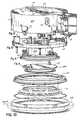
- FIG. 1Dis a disassembled perspective view of the IPVD source of FIG. 1C.
- FIG. 2is a disassembled perspective view of the housing portion of the IPVD source of FIGS. 1C and 1D.
- FIG. 3is a disassembled perspective view of the target assembly portion of the IPVD source of FIGS. 1C and 1D.
- FIG. 3Ais a fragmentary perspective view of a portion of the cover of the target assembly of FIG. 3.
- FIG. 4is an enlarged schematic cross-sectional view of the magnetron magnet assembly of the IPVD source of FIGS. 1C and 1D.
- FIG. 5is an enlarged cross-sectional view, similar to FIG. 4, illustrating an alternative magnet assembly.
- FIG. 6is a disassembled perspective view of the shield and window assembly of the IPVD source of FIGS. 1C and 1D.
- FIG. 6Ais a cross-sectional view of the circled portion of FIG. 6.
- FIG. 7is cross-sectional view of the RF source assembly of the IPVD source of FIGS. 1C and 1D.
- FIG. 8is a disassembled perspective view of the RF source assembly of FIG. 7.
- FIG. 9is an axial cross-sectional view of cooling manifold mounting assembly of the IPVD source of FIGS. 1C and 1D, the line along which the cross section is taken being illustrated in FIG. 13, described below.
- FIG. 10is an enlarged cross-sectional view of one embodiment of a fluid coupling assembly portion of the assembly of FIG. 9, the line along which the cross section is taken being illustrated in FIG. 13, described below.
- FIG. 11is an enlarged cross-sectional view of the mounting connector assembly of the assembly of FIG. 9 for the window and shield assembly of FIG. 6, the line along which the cross section is taken being illustrated in FIG. 13, described below.
- FIG. 12is an enlarged cross-sectional view of a DC con tact stub portion of the assembly of FIG. 9 of the IPVD source assembly of FIGS. 1C and 1D, the line along which the cross section is taken being illustrated in FIG. 13, described below.
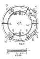
- FIG. 13is a top view of the magnet and cooling manifold mounting assembly portion of the IPVD source assembly of FIGS. 1C and 1D.
- FIG. 13Ais an enlarged view of the encircled portion marked 13 A in FIG. 13.
- FIG. 14is a disassembled perspective view of the IPVD source flange and dark space shield of the IPVD source assembly of FIGS. 1C and 1D.
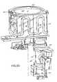
- FIG. 15is a bottom perspective view of the electrostatic chuck wafer support assembly of the apparatus of FIG. 1.
- FIG. 16is a side disassembled perspective view of the wafer support and lifting assembly portion of the apparatus of FIG. 1 for the wafer support of FIG. 15.
- FIG. 17is an axial cross-sectional view of the wafer support assembly portion FIG. 16.
- FIG. 18is a perspective view of the wafer support vertical position adjustment assembly of the apparatus of FIG. 1.
- FIG. 19is a top perspective view of the vacuum chamber wall assembly of the apparatus of FIG. 1.
- FIG. 20is a side perspective view of the lower portion of the apparatus of FIG. 1 showing particularly the vacuum chamber wall assembly of FIG. 19 and the gas vacuum system portion of the apparatus.
- FIG. 21is a schematic diagram of the gas vacuum system of FIG. 20.
- FIG. 22is a disassembled perspective view of the sputter shield portion of the chamber wall assembly of the apparatus of FIG. 1.
- FIG. 23is a disassembled perspective view of the IPVD source hoist mechanism of the apparatus of FIG. 1.
- the IPVD apparatus 500includes a vacuum chamber 501 bounded by a chamber wall assembly 502 .
- the chamber 501is provided with an IPVD source 503 supplying coating material in vapor form into the volume of the sputtering chamber 501 and for ionizing the sputtering material vapor; an electrostatic chuck wafer support system 507 for holding wafers during processing; a wafer handling system 504 , 504 a for loading and unloading wafers for processing; a vacuum and gas handling system 505 (FIGS.
- control system 509which operates the other systems of the apparatus 500 in accordance with the methods and processes described herein and otherwise carried out with the apparatus 500 .
- the apparatus 500is a serviceable module capable of providing features and operating conditions including the following: (1) base vacuum of less than 10 ⁇ 8 Torr, (2) operating inert gas pressure of between 30 and 130 mTorr, (3) provision for reactive gas at partial pressure of 0-50 mTorr, (4) variable substrate-to-target spacing of 6 to 9 inches, (5) electrostatic chucking with backside gas heating or cooling, and (6) shielding that restricts deposition to removable, cleanable components with surfaces having good adhesion of sputtered material to prevent particle generation.
- IPVD source 503The general concepts of the IPVD source 503 are described in U.S. patent application Ser. No. 09/073,141, hereby expressly incorporated herein by reference.
- the particular implementation of the source 503includes a ring-shaped target 10 of a type laid out in that application, particularly one of a frusto-conical shape.
- the principle objectives of the IPVD source 503include providing the following features and properties: (1) to require minimum operator effort and smallest possible set of tools to perform routine tasks, (2) to provide separation of RF and DC power from any water or other cooling fluid to the best extent possible, (3) to provide relative simplicity of design and operation, (4) to allow rapid repair or replacement of the source including quick replacement of the whole internal source assembly, rapid change of the target and of the various chamber shields, (5) to provide modular internal assemblies, and (6) to maintain RF shielding integrity to prevent leakage of radiation into the operating environment.
- the IPVD source 503rests upon the top of the wall 502 and is provided with a source flange and dark space ring assembly 470 that forms a vacuum tight seal with the wall 502 around the perimeter of a circular opening 412 in the top of the chamber wall 502 .
- the IPVD sourceincludes the annular target 10 and an RF source assembly 450 , which energizes an inductively coupled plasma in the chamber 501 .
- the RF source assemblyis situated in an opening 421 inside of the annulus of the target 10 , opposite a wafer, for example, a 200 mm or 300 mm wafer, 100 which is to be mounted on an electrostatic chuck 97 of the wafer support system 507 .
- the source 503includes a source housing assembly 410 that includes a source housing 1 (FIG. 2), which is preferably an aluminum weldment.
- the source housing 1includes structure for mounting the working parts of the source 503 , and coupling structure 411 for rendering the source 503 capable of being engaged, lifted, and lowered by the source hoist assembly 460 for installation on, and removal from, the apparatus 500 , as illustrated in FIG. 1A.
- the IPVD source 503can be rotated and thus inverted by the hoist 460 from its operative, downwardly facing orientation (FIGS. 1 and 1A) to the upwardly facing orientation of FIG. 1B in which the source 503 can be serviced, for example, to replace the target 10 or to remove other components of the source 503 for cleaning or servicing.
- the IPVD source 503is the source of the coating material and the ionization energy for producing the ionized coating material for deposition by the IPVD apparatus 500 .
- Target sputtering poweris brought into the housing 1 via a connector 2 .
- the target sputtering poweris DC power supplied by a DC power supply (not shown) on the apparatus 500 .
- the target poweris provided by an RF power supply.
- the power connector 2mates to a connector 2 a permanently mounted on the chamber wall 502 when the source 503 is installed in its operating position on the top of the chamber 501 .
- a negative DC feed 147passes through watertight strain relieving bushings 149 to a socket 3 mounted in an insulating block 4 inside the housing 1 while a positive feed 148 is connected directly to the housing 1 , which is typically maintained at the system ground potential.
- Ports 5are provided in the top of the housing 1 through which pass conductors 40 (FIG. 7) for RF connections 152 to an RF tuner 96 (FIG. 2) of an inductively coupled plasma (ICP) generator (FIGS. 6 - 8 ) on top of the source housing 1 .
- the autotuner 96is a commercial unit that mounts to the top of the source housing 1 (FIG. 2). Large female connectors 40 a supply power to the RF coil assembly 450 via connectors 40 (FIGS. 7 - 8 ). Outside of the housing 1 , RF cables connect the RF tuner 96 to an RF generator (not shown) on the apparatus 500 .
- the housing 1is also provided with an interlock switch 6 that detects the presence of the RF tuner unit 96 and the coil assembly 450 .
- An interlock switch 7is provided that is actuated by a pushrod mechanism 7 a , which is activated by a spring loaded pin 166 (FIGS. 9 and 13) to activate the switch 7 when the target 10 is properly installed.
- the interlock 7is provided to ensure that water and power cannot be supplied unless the target 10 is in place and locked down.
- a canted coil spring 8is provided that makes an electrical connection to a source flange and dark space ring assembly 470 surrounding a circular opening 412 in the top of the wall 502 of the chamber 501 .
- a plurality of, for example, three to six, hand-operated clips 9are provided at equally spaced intervals around the housing 1 , which, when released, allow the source flange and dark space ring assembly 470 to be removed and the target 10 to be changed or otherwise serviced, or to permit removal and replacement of the target 10 or the servicing of other components within the source housing 1 .
- Ports 150are provided for water inlet and outlet, and ports 151 are provided for a connection to a water loop external to the main source housing 1 .
- the target 10is part of a target assembly 420 , which is illustrated in FIG. 3.
- the target 10is frusto conical, and is designed to minimize manufacturing costs. It has a single upper O-ring groove 11 defining the upper vacuum coupling and a well-finished surface 427 which makes the lower coupling.
- the rear 428 of the target 10is smooth.
- the target 10may be monolithic as is usually the case when the target 10 is copper, or it may be formed by bonding a layer of source material to a structural backing plate by one of a number of techniques well known to sputtering engineers.
- the opposite sides of the targetdefine an included angle of divergence of a cone which is preferably about 110°.
- the 110° included angle of the conical target 10was selected after extensive computer modeling, using the HPEM code of Kushner et al. This angle leads to optimum uniformity of deposition at the pressures, powers, and target-substrate spacings of, preferably, about six to nine inches. A smaller included angle might also be desirable, but angles lower than 90 degrees are expected to lead to a reduction in deposition rate without much uniformity improvement. Higher included angles are expected to give poorer target utilization and poorer deposition uniformity.
- An O-ring groove 11is provided at the upper extreme of the target 10 at the inner edge of the target annulus around central opening 421 of the target 10 .
- Castellated features 12are provided to the outside of the O-ring groove 11 to allow the target 10 to assemble to a cooling water system 422 (FIG. 9) without the use of screws.
- a step 154is provided in the inside diameter around the opening 421 , which, in combination with a similar step in the window shield and window assembly 440 (FIG. 6). described below, prevents deposition of metal on a dielectric window 33 that covers the opening 421 also as described below.
- the target 10mates with a cooling cover 13 to define the cooling water system 422 .
- This cover 13has ‘quad ring’ water seals 14 and 15 on its inside on each side of a channel 16 . These seals 14 , 15 contact the rear of the target 10 when the target 10 and cover 13 are assembled.
- Bayonet assembly structure 153is provided which mates with the castellated features 12 on the target 10 to connect the cover 13 to the target 10 .
- slots 17are provided in the cover 13 to allow the cover 13 to be dropped over the castellated features 12 , after which the target 10 and cover 13 are rotated with respect to each other to produce a ‘jam jar’ effect that tightens the parts 10 , 13 together as they are rotated through about 20°, which is somewhat less than half of the angular spacing between the castellated features 12 and the matching bayonet assembly structure 153 .
- Water for target coolingenters and exits the cooling cover 13 via ports 155 into manifolds 18 formed in a ring-shaped channel 16 in the front surface of the cover 13 , as illustrated in FIG. 3A. These ports 155 and manifolds 18 are located 180° from each other around the channel 16 in the cover 13 .
- the manifolds 18are deeper than the channel 16 and each occupy about a 10° sector of the channel 16 .
- On each side of each manifold 18is a groove 19 a that accepts a comb 19 .
- Each comb 19is a thin metal insert that bears a series of notches 19 b .
- notches 19 bdivide water into separate streams as it enters the main channel 16 , avoiding the formation of stagnation regions in the water flow which could lead to a reduction of cooling efficiency or possible local boiling of the water.
- the design of the combs 19is determined by computational flow dynamics modeling.
- the combs 19may be removed and replaced with others designed for different flow rates versus pressure relationships without removal and replacement of the entire cover 13 .
- the cover 13may be removed from the expired target and reused.
- Water couplingis made through the cover 13 into the manifolds 18 via spring loaded water couplings 69 (FIGS. 9 - 10 ) which are described below.
- DC poweris connected via a spring loaded stub 80 (FIG. 12), described below.
- the IPVD source 503includes a magnetron magnet assembly 430 , illustrated in FIG. 4, which includes a magnet pack 20 that connects to the back of the target assembly 420 .
- the magnet pack 20includes a steel yoke 21 and a series of magnets 22 arranged in three rings including an inner ring 22 a , an intermediate ring 22 b and an outer ring 22 c , as shown.
- the resulting field lines produced by the magnets 22include a main magnetic tunnel 26 , which affects the target erosion at the beginning of a target life and runs in a circular path along an intermediate radius of the annular target 10 , and inner and outer magnetic tunnels 27 and 28 , respectively, which distribute the target erosion toward the inner and outer rims of the target annulus toward the end of the target life.
- the erosion groove due to this arrangementthereby broadens as the target erodes leading to enhanced target material utilization.
- the magnets 22are held in their locations by adhesive bonding.
- Non-magnetic rings 23may be used to space the magnets correctly, and the assembly may be encased in a molded plastic material body 24 having a convenient shape for mounting to the source housing 1 .
- FIG. 5An alternative magnetic arrangement is shown in FIG. 5. This simpler design is expected to lead to lower target utilization than that shown in FIG. 4.
- the magnet assemblies 20are preferably designed so that at least a portion of a magnetic tunnel traps plasma over the target 10 so that a net erosion of the target 10 takes place at all times over the target life so that no net redeposition takes place on the target 10 .
- One way this can be achievedis by placing the intermediate magnet ring 22 b sufficiently far from the target so that its field does not cancel the tunnel formed by field lines of the main tunnel 26 that extend between the opposite poles of the inner and outer magnet rings 22 a and 22 c.
- the magnet packscontain a number of holes 25 bored parallel to the axis which carry the feedthroughs for water and DC power leading to the target.
- the assembly of magnets 22is coated with a hard polymer coating such as polyurethane or enclosed within non-magnetic metallic or plastic cladding pieces, which are bonded to the magnet pack 20 . This coating prevents the magnets 22 and yoke 21 from becoming oxidized in air and also prevents the magnets 22 , which may be of sintered construction, from becoming a contaminating particle source.
- the IPVD source 503also includes a window and window shield assembly 440 , which is illustrated in FIG. 6.
- the shield and window assembly 440includes a dielectric window 33 , formed of a lapped, high purity alumina plate 7 mm thick, and a window shield 26 , formed of an electrically conductive material such as aluminum or copper.
- the shield 26is preferably made of metal and may function as a Faraday shield.
- the shield 26has an integral cooling water channel 27 formed therein and defined between an annular rim portion of the shield 26 and an annular channel cover ring 27 a braised or welded to the rim 27 a of the shield 26 .
- a number of slots 28are milled into the shield 26 .
- the slots 28are preferably chevron-shaped in cross section, as illustrated in FIG. 6A, or have some other cross section that blocks line of sight paths and protects the window 33 from direct deposits of coating material from within the chamber 501 .
- the dimensions of the slots 28are optimized by computer modeling to balance transparency of the shield 26 to RF energy against minimum transmission of sputtered material from the process region of the chamber 501 to the dielectric window 33 .
- Water connection to the channel 27 of the shield 26is made via stainless steel stubs 29 which thread into the shield 26 and make a water seal via O-rings 30 .
- Each of the stubs 29has external threads 31 and a conical tapered end 32 on which a smooth finish has been placed.
- the assembly of the shield 26 with stubs 29 attachedis assembled to the window 33 by inserting the stubs 29 through holes 34 in the dielectric window 33 , which align with holes 34 a , which are 180° apart around the rim of the shield 26 and which communicate with the channel 27 .
- TEFLON washers 35 and aluminum knurled nuts 36are screwed onto the stubs 29 and compress O-rings 37 between the window shield 26 and the window 33 forming a vacuum seal around the water stubs 29 .
- O-rings 38are provided in the nuts 36 , which have no sealing function but perform the function of a spring, helping to prevent over-tightening of the nuts 36 .
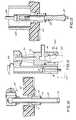
- a dense secondary plasma for ionizing material that has been sputtered from the target 10is excited by an RF coil assembly 450 , illustrated in FIG. 7, which includes a three-dimensional coil 39 whose configuration and electrical performance and properties are described in U.S. patent application Ser. No. 09/277,526, filed on Mar. 26, 1999, entitled Process Apparatus And Method For Improving Plasma Distribution And Performance in an Inductively Coupled Plasma, invented by Jozef Brcka, an inventor herein, hereby expressly incorporated herein by reference.
- the RF feeds to the coilare provided by a pair of male connectors 40 that thread into sockets 41 in the coil end pieces 42 . Water feed is provided through a pair of threaded pipe couplings 43 . These couplings are surrounded by a flange 44 with an O-ring groove 45 .
- the coil 39is mounted within a high dielectric insulating cup 46 made of a material such as TEFLON.
- the thickness of material of the cup 46 in various areas of the cup surfaceis calculated to be as thin as possible consistent with the suppression of arcing to the nearest conductive surface.
- the effective field and pressure-distance product in airare calculated for the stack consisting of the TEFLON, an air gap, and any other dielectric such as the source window 33 .
- the thickness of TEFLONcan be set so that the field is always lower than that required to cause breakdown of air, for reasonable values of the air gap. This calculation allows the cup thickness to be minimized safely.
- a minimum thicknessallows the best coupling to the plasma and lessens the constraints on the dimensions of the coil 39 .
- the cup 46is mounted in an aluminum ring 47 .
- This ringis mounted to the water cooling assembly 422 using shoulder screws 62 and springs 63 which, in operation, press the ring against the dielectric window 33 which is part of the window and shield assembly 440 described above.
- This window 33is pressed against the target upper O-ring 48 , which is located in the groove 11 .
- This spring loadingcompensates for tolerance mismatch and mechanical deformation and so holds the vacuum seals together and allows the system to be pumped down.
- the ring 47also features a canted coil spring 49 and a tube 50 for cooling water.
- Recesses 52are provided around the holes 51 in the back of the ring 47 for TEFLON washers 53 .
- An aluminum enclosure 54is mounted over the coil 39 and held down by a bolt circle so that there is electrical continuity through the canted coil spring 49 , to the aluminum ring 47 .
- the purpose of thisis to prevent water leaks, if any, from reaching the high voltages present on the coil and to act as a primary barrier to RF emission from the source. RF energy can escape only through the dielectric window 33 into the process space of the chamber 501 .
- the enclosureis pierced in four places, two ports 55 carrying RF feeds and two ports 56 carrying water feeds for the coil 39 .
- TEFLON parts 57are passed through the water feed ports 56 and pass over O-rings 45 making a water seal.
- TEFLON insulating pieces 58are used to stand the coil and RF connectors off electrically from the enclosure.
- TEFLON combs 59are used with insulating screws to hold the coil down to the cup 46 . This leads to consistent behavior between different sources.
- cooling wateris distributed via components mounted on a large plastic plate 60 which also supports the magnet assembly 430 , which is mounted thereto on spacers 61 , and the RF source assembly 450 , which is mounted thereto using the shoulder screws 62 .
- a main aluminum manifold block 64is mounted to the plate 60 and brings in water from the exterior of the source via threaded connections.
- a secondary manifold 65allows the flow of water through the coil to be checked by a flow sensor mounted outside the source and also allows connection of the water flow to a cooling channel in the source flange and dark space ring assembly 470 .
- Cooling water for the target 10passes through stub assemblies 68 , as illustrated in FIG. 10.
- the assemblies 68are designed so that water couplings 69 can be assembled through holes no larger than the outer diameter of the coupling tubes themselves; which allows the holes 25 in the magnet pack to be of minimum diameter, which minimizes the disturbance of the magnetic field that these holes might cause.
- the assemblies 68are spring loaded, the springs 70 acting between metal cups 71 that are pressed into the plastic mounting block 60 and washers 72 that are held in place on the water tubes 69 by retaining rings 73 . In this way, in operation, the lower end of the cooling tube bears on an O-ring 74 that is forced into a specially designed detail in the target cooling cover 13 .
- the detailis a doubly tapered bore similar to that used in ISO and SAE standard fluid connecting glands.
- the window shield 26is cooled via special couplings 75 that also make a DC connection 423 to the shield, as illustrated in FIG. 11.
- the couplingfeatures a tapered recess with an inward facing O-ring 76 .
- the entire fittingis spring loaded via springs 77 ; and when assembled, the tapered surface of the stub 29 is forced hard against the O-ring 76 ; making a water seal.
- the canted coil spring 77performs a double function. Firstly, it makes electrical connection to the shield 26 . Secondly, it performs a latching function, engaging a shallow recess in the stub 29 which holds the shield 26 approximately in place after it has been installed to the water housing 422 .
- this couplingbears a tapped hole 78 for making electrical connections.
- the couplinginserts into the RF assembly through the TEFLON washers 53 .
- Support blocks 79are mounted on the block 60 and support the coupling, and they also apply pressure to the springs 77 , These blocks are fitted at their upper end with contact fingers 156 which ground the entire assembly, and through it the Faraday shield, when the source is assembled, by making contact to the source housing 1 .
- the block 60also contains supports for two non-water-related items.
- Oneis the DC contact stub 80 , which is spring loaded similarly to the target water couplings, as illustrated in FIG. 12.
- the stub 80is forced against the target cooling cover, contact being ensured by another canted coil spring 81 .
- the upper end of the stubis fitted with a male connector 158 .
- This DC connector stub assemblyis surrounded by a plastic tube 159 that protects it from spray in the event of a water leak in the source.
- the other itemis a spring-loaded pin 166 (FIG. 9) that passes through the magnet pack and bears against the target cooling cover 13 (FIG. 3).
- this pin 166bears on another plunger assembly 7 a described above, which, in turn, activates a microswitch 7 .
- the activation of this switch 7indicates that the target assembly 420 is correctly installed and, therefore, that it is safe to turn on the cooling water.
- the water distribution assembly 422contains a number of couplings and a considerable length of TEFLON hose. In the event of a leak developing, it is desirable that water be drained to the exterior of the source and taken somewhere it can be detected. Therefore, the block 60 contains a pattern 82 of drainage grooves that terminate at small holes 83 (FIG. 2) in the source housing 1 .
- Vacuum leak checking of the sourceshould be carried out.
- the inner target O-ring as well as the window seal O-ringsare rather relatively inaccessible.
- the block 60is also provided with stainless steel capillary tubes 84 , which are embedded into some of the grooves 82 as shown in FIG. 13A. During leak checking, these tubes 84 can be used to feed helium to the vicinity of the inaccessible O-rings.
- the source flange and dark space ring assembly 470is illustrated.
- This assembly 470includes a source flange 67 on which is mounted the fixed parts 86 corresponding to the clips 9 .
- a swaged-in cooling water tube 471is provided.
- the upper sidebears a recess 87 with an O-ring groove 88 into which is inserted a TEFLON insulator 89 , which is itself provided with an O-ring groove 90 .
- Weep holes 472are provided leading from the recess 87 to the outside diameter of the flange, which provide drainage and visual warning in the event of a cooling water leak.
- the O-ring groove 90bears an O-ring 90 a that interfaces to the target 10 , forming the outer vacuum seal.
- the underside of the source flange 67has another recess into which is mounted the dark space shield 91 .
- This shield 91is held in place by shoulder screws 92 that tighten into slot features 93 .
- the screws 92are slightly loosened and the shield 91 then slightly rotated and lifted off.
- the shield 91is designed so as to not contact the source flange 67 in regions near the O-ring groove 88 to avoid overheating of that O-ring.
- the source flange 67interfaces electrically to the process chamber electrically, using a canted coil spring 94 .
- An O-ring 95makes the vacuum seal.
- IPVD source 503There are several features or considerations relating to the IPVD source 503 . Assembly and dismantling for repairs is one. In assembly, the fully assembled source interior (less Faraday shield assembly 440 and target assembly 420 ) is dropped into the upturned source housing assembly so that the DC connector 158 (FIG. 12) inserts into the socket 4 (FIG. 2). Six screws are inserted and water connected to four ports 151 , 152 . Electrical feeds are plugged in. The source 503 is then ready for use. Dismantling is the reverse of assembly. This simple assembly technique is an advantage of the modular construction of the source. Routine target replacement is another such feature or consideration. After cooling water has been blown out, the source 503 is inverted and the clips 9 released. The flange assembly is then lifted off. The target then can be lifted out and then the Faraday shield assembly can be removed. No tools are needed except to release the dark space shield 91 .
- the electrostatic chuck 507 and the wafer transfer system 504cooperate in the transfer of wafers from one to the other.
- the chuck assembly 507includes a service support assembly 480 as illustrated in FIG. 15, which includes the wafer support, holder or chuck 97 .
- a suitable chuck 97may be obtained from INVAX Inc. or other sources.
- a fluid passageis provided for the passage of cooling fluid, for example, a GALDEN brand perfluorinated fluid.
- the chuck 97is of the tripolar type, having two embedded, electrically isolated, electrodes for the application of a chucking voltage, while RF bias can be applied to the chuck body by way of the electrostatic chuck electrodes. The RF is thereby coupled through to the embedded electrodes and thus to the wafer. All metal parts of the chuck are aluminum coated with a proprietary dielectric. Back side gas can be provided through a central hole.
- a thermocoupleis mounted to the rear of the chuck.
- the chuck 97has a number of counterbored holes and is mounted to the stainless steel base 98 using screws; there are polyimide ‘vespel’ insulators that protect the chuck from damage by the screws and provide electrical isolation.
- An insulating block 99isolates the chuck from the base.
- FIG. 16shows the mounting of the chuck to its support structures.
- the stainless steel base 98is fitted with rest pegs 101 , which support a ring 102 .
- the ringhas features which work with those on the rest pegs to give an accurate alignment of the ring with the chuck.
- This ringhas sockets 103 that are fitted with ceramic lift pins 104 , which pass through holes in the chuck.
- the ring 102rests on the pegs 101 during process.
- the basehas a short downward extending tube at the end of which is a flange 119 that can be clamped to the Z drive assembly 490 described below.
- FIG. 22Two configurations of shields for this table are shown in FIG. 22.
- a stainless shield 105rests on a step on the base 98 and shields the chuck from metal deposition.
- a grounded shield 106is supplemented by a ring 107 , which rests directly on the chuck.
- This ringmay be made of aluminum or stainless steel and may, or may not, be coated with a dielectric material, possibly of high dielectric constant similar to that used in the chuck dielectric. This ring couples to the RF power that is applied to the chuck through the chuck dielectric.
- the shieldcan be in very close proximity to the chuck, thereby more effectively blocking metal deposition; and that RF power is applied to the ring causing it to attain the same bias as the wafer, which lessens the distortion of electric fields near the wafer edge.
- the ringoverlaps but is separated from the grounded shield. This provides a convoluted path for metal deposition and keeps material from being deposited on the chuck.
- the wafer transfer mechanism 504illustrated in FIG. 18, is attached to the base of the chamber wall assembly 502 (FIG. 19) using the threaded pegs 108 .
- a ring 109is held in a raised position by springs 110 . It is held in an accurate position by the features 111 and 112 .
- Slotted pegs 113are mounted to this ring. When the table or chuck is lowered, the pegs 101 descend into the slots 114 in the slotted pegs. The ring 102 is lifted and the pins 104 raised. When the pins have lifted llmm, the pegs 101 reach the bottom of the slots 114 . Usually the transport system would now insert a pick to collect the wafer.
- Service support assembly 480includes a rigid assembly 116 , formed by three silver plated brass tubes 117 with nylon spacers 118 at regular intervals and a silver plated plate at each end, is fixed to the chuck with screws. It has a triple function that includes: (1) mechanical support of the chuck voltage wires, thermocouple wires, temperature control fluid tubes, and backside gas tube; (2) RF power conduction to the chuck body; and (3) conduction of nitrogen purge gas to the space behind the chuck. At low operating temperatures, water condensation hinders chuck operation unless a gas purge is provided to sweep out moisture. In this case there are small cross holes in the support tubes near the interface to the chuck. Purge gas is connected at the lower end of the tube.
- the vertical elevator or Z drive system 490 for vertically moving and adjusting the height of the chuck 97is illustrated in FIG. 18.
- Thisconsists of a tube 120 with an upper flange that can be coupled to the table flange 119 using clamps 121 .
- a rail 122is mounted to the tube which rides in sliders 123 which are supported on a bracket 124 .
- a ball nut 125 mounted to a flange 126 at the lower end of tube 120is driven by a lead screw 127 .
- This screwis turned by a motor and gearbox combination 128 .
- the motoris fitted with a brake (not shown) that prevents backdriving of the motor when it is turned off.
- the motor control systemis conventional.
- Position of the tableis determined using an encoder mounted at the upper end of the lead screw.
- the bracket 124is mounted to the process chamber.
- a backside gas delivery system and components enclosure 129is mounted below the flange 126 .
- This enclosurecontains electronics for conditioning of signals running to and from the chuck.
- the table RF autotuner 130a commercial unit, is mounted to the exterior.
- valves and a universal pressure controllerare mounted to the exterior of the enclosure 129 . These components control the backside gas delivery. In the future, these components will be moved to a position elsewhere.
- a plasma arrestoris used to form an insulating break in the backside gas system and avoid plasma formation in the gas line.
- the vacuum and gas handling system 505is illustrated in the diagram of FIG. 21.
- Thisincludes a chamber and pumping system.
- the chamber 501is contained within a chamber wall assembly 502 which includes, particularly, a vacuum tight chamber enclosure 131 as illustrated in FIGS. 19 and 20, which is of a conventional stainless steel design.
- the enclosure 131has an internal isolation valve 132 for coupling to a handler of the transfer system 504 .
- An eight inch conflat flange in the basecouples to an isolation valve 142 , and this is connected to a cryogenically cooled panel 143 operating at about 110K and a turbomolecular pump 144 .
- the speed of the turbo pumpcan be controlled to allow for processing at relatively high gas pressures in low speed (about 24000 RPM) operation while rapid pump-down from atmospheric pressure is provided at high pump speeds (350 ls ⁇ 1 nominal at about 56000 RPM).
- the turbo pumpis backed by a non oil sealed type rotary pump 145 which is also used to pump the chamber down to 100 mTorr or so after venting at which pressure the isolation valve may be opened.
- the vacuum arrangementis quite conventional except for the use of the water pump/variable speed turbo pump combination.
- the chamberhas external water cooling channels for cooling during normal operation.
- a flangeis provided for mounting of the source hoist.
- the chamberis locally stiffened around this flange by the addition of external welded ribs, to support the loads exerted when the source is raised by the hoist.
- a housing for the DC connector 162 for the sourceis also mounted on the chamber.
- FIG. 21The gas systems for modules with and without reactive gas are shown in the schematic diagrams of FIG. 21. Delivery of argon gas to the chamber is via a simple flange. Reactive gas, if used, passes into a branched ‘spider’ tube 133 , which carries it into the process space. The tubes end in two positions on opposite sides of the table assembly. Small covers 134 rest on the ends of the gas tubes to prevent deposition of sputtered material on the gas tubes.
- a sputter shield assembly 495is provided as illustrated in FIG. 22. These are among five shields that are subject to removal and cleaning. These are the Faraday and dark space shields described above, the table shields described above, and two chamber shields 136 , 137 . These chamber shields are supported on an armature 138 . Upper shield 136 , which typically rises to a higher temperature than lower shield 137 , is supported at three points on the pegs 139 rising from the armature. Features 140 on the shield 138 rest on these pegs, centering the shield in the chamber but allowing radial motion. This avoids the buildup of stresses in the shield due to thermal expansion and deposition of hot material with subsequent differential thermal expansion.
- the shieldrequires no tools to remove it.
- the lower shield 137is inserted into the armature 138 and is supported by it. Self centering behavior arises from the chamfer 141 in the armature. No tools are required to remove the shield.
- the gap between the shields 136 , 137is well controlled and pumping occurs all around the circumference of the process region in a controlled way.
- the height of shield 136controls the gap between the source dark space shield and the shield 136 .
- This gapis designed to be small, preferably of the order of one millimeter, to reduce the passage of metal through the gap.
- the shield 136fits in a recess in the dark space shield, forming a convoluted path that intercepts metal that enters the gap between the shields before the unprotected regions of the chamber are reached. Good dimensional specification is necessary to achieve this as is attention to the thermal expansion of the parts.
- the waferis loaded through a slot 146 in the lower shield 137 .
- this slot 146is closed off by the table shield 105 or 106 .
- the slot 146may also have a surround 147 to intercept sputtered metal more efficiently.
- the source hoist 460is illustrated in FIG. 23.
- the source hoist 460is a pneumatic lift capable of raising a weight of about 200 pounds. It is required to lift the source off the chamber; it must then rotate about a vertical axis. There must also be a motion allowing the source to be turned over for target removal. The source must be lowered for easier access to the target.
- Considerable rigidity of the assemblyis required in order that the source be maintained level when lifted off the top of the wall 502 of the chamber 501 .
- a pneumatic cylinder 173allows the raising and lowering of the source.
- Item 171is intended to move vertically and also to rotate while item 172 rotates only, being kept aligned with item 171 by the cylinder.
- Rollers 174act as bearings on which the upper assembly 172 rotates. There are recessed features 174 into which these rollers can drop. This provides some resistance to the rotation of the assembly at certain points, allowing the operator to detect the correct positions for operation.
- Assembly 176contains a pair of opposed angular bearings. Shaft 177 passes through these and is retained by a cap 178 and a spring washer 179 that pre-loads the bearings. This arrangement leads to a rotational joint with very high radial rigidity.
- the assembly 176also contains a cam wheel feature that, in conjunction with a plunger 180 , ensures that the source can only be rotated in one direction and can be locked in its upright and inverted orientations.
- the hoistmounts to the source using the flange 181 .
- Preferred process parameters for the deposition of tantalum and tantalum nitride in one module 500 and then deposition of copper in another module 500 of the same cluster toolare as follows: DC ICP RF Table Pres- N 2 Flow Table Power Power Power sure (% of total Temperature Film (kW) (kW) (W) (mT) flow) (° C.) Cu 8 to 15 1 to 5 0 to 100 50 to 75 — ⁇ 50 to 0 Ta 8 to 12 1 to 5 0 to 150 80 to — 50 to 100 120 TaN x 8 to 12 1 to 5 0 to 200 80 to 3 to 25 50 to 100 120
Landscapes
- Chemical & Material Sciences (AREA)
- Engineering & Computer Science (AREA)
- Physics & Mathematics (AREA)
- Plasma & Fusion (AREA)
- Analytical Chemistry (AREA)
- Chemical Kinetics & Catalysis (AREA)
- Materials Engineering (AREA)
- Mechanical Engineering (AREA)
- Metallurgy (AREA)
- Organic Chemistry (AREA)
- Physical Vapour Deposition (AREA)
Abstract
Description
- This application is a continuation of PCT application no. PCT/US00/31756, filed, which claims priority in part to U.S. patent application Ser. No. 09/442,600 of John Drewery et al., filed Nov. 18, 1999, hereby expressly incorporated herein by reference.[0001]
- This invention relates to the Ionized Physical Vapor Deposition (IPVD) and, more particularly, to methods and apparatus for depositing films, most particularly metal films, onto semiconductor wafer substrates by sputtering the coating material from a target, ionizing the sputtered material, and directing the ionized coating material onto the surface of the substrates.[0002]
- Ionized physical vapor deposition is a process which has particular utility in filling and lining high aspect ratio structures on silicon wafers. In IPVD, for deposition of thin coatings on semiconductor wafers, materials to be deposited are sputtered or otherwise vaporized from a source and then a substantial fraction of the vaporized material is converted to positive ions before reaching the wafer to be coated. This ionization is accomplished by a high-density plasma which is generated in a process gas in a vacuum chamber. The plasma may be generated by magnetically coupling RF energy through an RF powered excitation coil into the vacuum of the processing chamber. The plasma so generated is concentrated in a region between the source and the wafer. Then electromagnetic forces are applied to the positive ions of coating material, such as by applying a negative bias on the wafer. Such a negative bias may either arise with the wafer electrically isolated, by reason of the immersion of the wafer in a plasma, or by the application of an RF voltage to the wafer. The bias causes ions of coating material to be accelerated toward the wafer so that an increased fraction of the coating material deposits onto the wafer at angles approximately normal to the wafer. This allows deposition of metal over wafer topography including in deep and narrow holes and trenches on the wafer surface, providing good coverage of the bottom and sidewalls of such topography.[0003]
- Certain systems proposed by the assignee of the present application are disclosed in U.S. patent applications Ser. Nos. 08/844,751; 08/837,551 and 08/844,756 filed Apr. 21, 1997, hereby expressly incorporated herein by reference. Such systems include a vacuum chamber which is typically cylindrical in shape and provided with part of its curved outer wall formed of a dielectric material or window. A helical electrically conducting coil is disposed outside the dielectric window and around and concentric with the chamber, with the axial extent of the coil being a significant part of the axial extent of the dielectric wall. In operation, the coil is energized from a supply of RF power through a suitable matching system. The dielectric window allows the energy from the coil to be coupled into the chamber while isolating the coil from direct contact with the plasma. The window is protected from metal coating material deposition by an arrangement of shields, typically formed of metal, which are capable of passing RF magnetic fields into the interior region of the chamber, while preventing deposition of metal onto the dielectric window that would tend to form conducting paths for circulating currents generated by these magnetic fields. Such currents are undesirable because they lead to ohmic heating and to reduction of the magnetic coupling of plasma excitation energy from the coils to the plasma. The purpose of this excitation energy is to generate high-density plasma in the interior region of the chamber. A reduction of coupling causes plasma densities to be reduced and process results to deteriorate.[0004]
- In such IPVD systems, material is, for example, sputtered from a target, which is charged negatively with respect to the plasma, usually by means of a DC power supply. The target is often of a planar magnetron design incorporating a magnetic circuit or other magnet structure which confines a plasma over the target for sputtering the target. The material arrives at a wafer supported on a wafer support or table to which RF bias is typically applied by means of an RF power supply and matching network.[0005]
- A somewhat different geometry employs a plasma generated by a coil placed internal to the vacuum chamber. Such a system does not require dielectric chamber walls nor special shields to protect the dielectric walls. Such a system is described by Barnes et al. in U.S. Pat. No. 5,178,739, expressly incorporated by reference herein. Systems with coils outside of the chamber, as well as the system disclosed in the Barnes et al. patent, involve the use of inductive coils or other coupling elements, either inside or external to the vacuum, that are physically positioned and occupy space between the planes of the sputtering target and the wafer.[0006]
- Whether a coupling element such as a coil is provided inside or outside of a vacuum chamber, dimensions of the system have been constrained by the need for adequate source-to-substrate separation to allow for the installation of the RF energy coupling elements between the source and the substrate. Adequate diameter must also be available around the wafer for installation of coils or other coupling elements. As a direct result of the increased source-to-substrate spacing due to the need to allow space for the coupling element, it is difficult to achieve adequate uniformity of deposition with such systems. If the height of the chamber is reduced to improve uniformity, there is a loss of plasma density in the central region of the chamber and the percentage of ionization of the coating material is reduced. Also, in practice, the entire system must fit within a constrained radius. As a result, there are frequently problems due to heating arising from the proximity of the RF coils to metal surfaces, which may necessitate extra cooling, which increases engineering and production costs and wastes power.[0007]
- An IPVD apparatus with the coil in the chamber has the additional disadvantage that the coils are eroded by the plasma and must, therefore, consist of target grade material of the same type as that being sputtered from the target. Moreover, considerable cooling of coils placed in the vacuum chamber is needed. If liquid is used for this cooling of the coils, there is danger that the coils will be penetrated, by uneven erosion or by arcing, causing a resulting leak of liquid into the system, which is highly undesirable and will likely result in a long period of cleaning and re-qualification of the system. Furthermore, an excitation coil in the chamber also couples capacitively to the plasma, leading to inefficient use of the excitation power and to the broadening of the ion energy spectrum, which may have undesirable effects on the process.[0008]
- The miniaturization of semiconductor devices has resulted in a need to form low resistance connections to contacts at the bottoms of high aspect ratio holes of a fraction of a micron in diameter. This has increased the demand for the use of highly electrically conductive metals, such as copper, over barrier layers of materials, such as tantalum and tantalum nitride. The techniques for depositing such materials in the prior art have not been totally satisfactory.[0009]
- The deposition of materials by PVD methods has, in the prior art, involved critical designs of sputtering sources to produce plasma concentrations of uniform geometries within sputtering chambers and to directly affect the distribution uniformities of the deposited films. The prior art approaches have resulted in compromises of other performance parameters to those ends.[0010]
- As a result of the above considerations and problems, there remains a need for more efficiently coupling energy into the dense coating material ionizing plasma in IPVD processing systems, and to do so without interfering with the optimum dimensions of the chamber and preferably without placing a coil or other coupling element into the vacuum chamber.[0011]
- One objective of the present invention is to provide an IPVD method and an IPVD apparatus in which the placement of the coil or other coupling element does not adversely affect the geometry of the chamber of the processing apparatus. Another objective of the present invention is to provide a more efficient and effective method and apparatus for the performance of IPVD.[0012]
- According to the principles of the present invention, an IPVD apparatus is provided with a ring-shaped source of coating material for producing a vapor that includes atoms or minute particles of the coating material to a processing space within a vacuum chamber. At the center of the ring-shaped source is provided a coupling element for reactively coupling RF energy into the chamber to produce a high-density, reactively coupled plasma in the processing space to ionize coating material passing through the processing space. The ions of coating material drift, whether under the influence of electrostatic or electromagnetic fields or otherwise, toward a substrate in the chamber, at the opposite end of the processing space from the source. Those ions that arrive within a certain distance, for example, in the order of a centimeter, from the substrate, encounter a sheath field and are accelerated toward the substrate so that a high percentage of the coating material arrives on the substrate at angles normal to the substrate, thereby more effectively lining the bottoms and sides of, or filling, small and high aspect ratio features on the surface of the substrate.[0013]
- In one embodiment of the invention, a coating material source, preferably a sputtering target, is provided with a central opening in which is placed a dielectric window. Behind the window, outside the vacuum of the chamber, is located a plasma source which includes a coupling element, preferably a coil, which is connected to the output of an RF energy source. The coupling element is configured to couple, preferably inductively, energy supplied from the energy source through the window at the opening at the center of the material source and into the region of the chamber between the coating material source and the substrate, such as a semiconductor wafer, on a substrate support at the opposite end of the chamber from the coating material source.[0014]
- The apparatus of the present invention includes an annular sputtering target which surrounds a central ceramic window. This annular target is preferably frusto conical in shape. A magnetron magnet assembly is positioned behind the target to produce a plasma confining magnetic field over the target, preferably in the shape of an annular tunnel on the surface of the annular target surrounding the central opening at its center.[0015]
- The coupling element is preferably a coil positioned behind and close to the back outside surface of the dielectric window at the central opening of an annular sputtering target. RF energy of, for example, 13.56 MHZ, is applied to the coil to excite a high-density inductively coupled plasma in the chamber between the target and the substrate. A main sputtering plasma that is trapped under the field of the magnetron magnets at the surface of the target, sputters coating material from the target and into the region of the processing space occupied by the dense secondary plasma, where a substantial portion of the material is stripped of electrons to form positive ions of the coating material. A negative bias voltage is applied to a wafer on the substrate holder, which attracts the positive ions of sputtering material from the region of the secondary plasma and toward and onto the surface of the substrate, with the angles of incidence approaching being perpendicular to the substrate so that they can enter trenches and holes on the wafer substrate to coat the bottoms of these holes and trenches.[0016]
- Certain embodiments of the apparatus and method of the invention include an IPVD source that employs a three-dimensional coil that energizes a dense inductively coupled three-dimensional plasma in three-dimensional regions within the chamber. The chamber is operated at a vacuum pressure of between 30 and 130 mTorr to essentially thermalize the plasma, so that ions of coating material can be formed in the plasma and electrically directed perpendicular to and onto the substrate, thereby reducing the effect of target and magnet configuration on coating uniformity. The IPVD source is coupled through a window into the chamber through a high dielectric material such as a TEFLON spacer and then through a dielectric window such as quartz which forms the vacuum barrier closing a circular opening in the chamber wall at the center of an annular target. Inside the chamber is a window shield having chevron-shaped slots therein oriented relative to the conductors of the coil. The shield protects the window from deposits, particularly deposits of metallic coating material, while passing inductively coupled RF energy into the chamber. The shield may further function as a Faraday shield, preventing capacitive coupling from the coil to the plasma and avoiding flux compression heating. The shield has integral cooling and is formed of cast copper which is plated with aluminum, so that the shield can be reconditioned by chemically dissolving aluminum coating to remove buildup and then re-plating the copper shield with aluminum for reuse. The window and shield assembly form a removeable combination. The window and shield are spaced so the window is self cleaning adjacent the slits in the shield by plasma that forms at this point in the slits.[0017]
- The target is preferably frusto conical, with the walls of the truncated cone inclined about 35° to the horizontal or plane of the window. A permanent magnet pack is employed which produces three, and preferably only three, magnetic tunnels over the target surface, with a main central tunnel dominating early in the target life to erode the mean radius of the annular target and two side tunnels taking over later in the life of the target to erode grooves adjacent the inner and outer rims of the target annulus.[0018]
- The apparatus preferably uses a wafer holder mounted for vertical motion on a Z-table motion drive to provide for target-to-substrate spacing (TSS) of from six to nine inches and to provide for wafer handoff to a transfer arm from a transfer module. The support is provided with an electrostatic chuck, and wafer heating and cooling is provided using a Peltier device remote from the support that connects through a GALDEN fluid loop with the support and through another fluid loop with a heat sink. The electrostatic chuck is tri-polar with the chuck grid serving as electrodes to provide[0019]2-zone bias to the wafer to attract the ionized sputtered material to the wafer. A shadow ring is provided around the edge of the wafer to provide non-contact edge masking.
- The chamber has a removable shield insert in two parts that mechanically float relative to each other to accommodate different expansions due to different heating. The shield assembly is a replaceable subcombination. The apparatus is particularly useful for depositing copper over tantalum and tantalum nitride and for depositing the underlying tantalum and tantalum nitride barrier layer over a patterned wafer, with Ta deposited by ionized PVD and TaN deposited by PVD in the same chamber, followed by deposition of copper by ionized PVD in a similar module attached to a transfer module of the same tool. The copper so deposited is suitable to be followed by any of many methods of Cu fill, particularly by electroplating. The processes are preferably carried out using process parameters, including: pressures, temperatures, gases, bias power and/or voltage levels, sputtering power levels, IC power levels, etc., as described below.[0020]
- With apparatus structure according to the invention, the processing chamber can be dimensioned to provide optimum spacing between the coating material source and the substrate to provide both good ionization of sputtered species as well as good uniformity of deposition on the wafers.[0021]
- The present invention provides greater freedom of design choice in configuring the processing chamber to optimize the IPVD process, and does so while overcoming the difficulties set forth in the background above.[0022]
- These and other objectives and advantages of the present invention will be more readily apparent from the following detailed description of the drawings.[0023]
- FIG. 1 is a schematic cross-sectional diagram of one embodiment of IPVD apparatus according to the present invention.[0024]
- FIG. 1A is a cross-sectional diagram similar to FIG. 1, illustrating the apparatus with the IPVD source being removed.[0025]
- FIG. 1B is a diagram, similar to FIG. 1A, illustrating the IPVD source of the apparatus with the source flange and target assembly being removed.[0026]
- FIG. 1C is a partial cross-sectional diagram of the IPVD source of the apparatus of FIG. 1, the line along which the cross section is taken being illustrated in FIG. 13, described below.[0027]
- FIG. 1D is a disassembled perspective view of the IPVD source of FIG. 1C.[0028]
- FIG. 2 is a disassembled perspective view of the housing portion of the IPVD source of FIGS. 1C and 1D.[0029]
- FIG. 3 is a disassembled perspective view of the target assembly portion of the IPVD source of FIGS. 1C and 1D.[0030]
- FIG. 3A is a fragmentary perspective view of a portion of the cover of the target assembly of FIG. 3.[0031]
- FIG. 4 is an enlarged schematic cross-sectional view of the magnetron magnet assembly of the IPVD source of FIGS. 1C and 1D.[0032]
- FIG. 5 is an enlarged cross-sectional view, similar to FIG. 4, illustrating an alternative magnet assembly.[0033]
- FIG. 6 is a disassembled perspective view of the shield and window assembly of the IPVD source of FIGS. 1C and 1D.[0034]
- FIG. 6A is a cross-sectional view of the circled portion of FIG. 6.[0035]
- FIG. 7 is cross-sectional view of the RF source assembly of the IPVD source of FIGS. 1C and 1D.[0036]
- FIG. 8 is a disassembled perspective view of the RF source assembly of FIG. 7.[0037]
- FIG. 9 is an axial cross-sectional view of cooling manifold mounting assembly of the IPVD source of FIGS. 1C and 1D, the line along which the cross section is taken being illustrated in FIG. 13, described below.[0038]
- FIG. 10 is an enlarged cross-sectional view of one embodiment of a fluid coupling assembly portion of the assembly of FIG. 9, the line along which the cross section is taken being illustrated in FIG. 13, described below.[0039]
- FIG. 11 is an enlarged cross-sectional view of the mounting connector assembly of the assembly of FIG. 9 for the window and shield assembly of FIG. 6, the line along which the cross section is taken being illustrated in FIG. 13, described below.[0040]
- FIG. 12 is an enlarged cross-sectional view of a DC con tact stub portion of the assembly of FIG. 9 of the IPVD source assembly of FIGS. 1C and 1D, the line along which the cross section is taken being illustrated in FIG. 13, described below.[0041]
- FIG. 13 is a top view of the magnet and cooling manifold mounting assembly portion of the IPVD source assembly of FIGS. 1C and 1D.[0042]
- FIG. 13A is an enlarged view of the encircled portion marked[0043]13A in FIG. 13.
- FIG. 14 is a disassembled perspective view of the IPVD source flange and dark space shield of the IPVD source assembly of FIGS. 1C and 1D.[0044]
- FIG. 15 is a bottom perspective view of the electrostatic chuck wafer support assembly of the apparatus of FIG. 1.[0045]
- FIG. 16 is a side disassembled perspective view of the wafer support and lifting assembly portion of the apparatus of FIG. 1 for the wafer support of FIG. 15.[0046]
- FIG. 17 is an axial cross-sectional view of the wafer support assembly portion FIG. 16.[0047]
- FIG. 18 is a perspective view of the wafer support vertical position adjustment assembly of the apparatus of FIG. 1.[0048]
- FIG. 19 is a top perspective view of the vacuum chamber wall assembly of the apparatus of FIG. 1.[0049]
- FIG. 20 is a side perspective view of the lower portion of the apparatus of FIG. 1 showing particularly the vacuum chamber wall assembly of FIG. 19 and the gas vacuum system portion of the apparatus.[0050]
- FIG. 21 is a schematic diagram of the gas vacuum system of FIG. 20.[0051]
- FIG. 22 is a disassembled perspective view of the sputter shield portion of the chamber wall assembly of the apparatus of FIG. 1.[0052]
- FIG. 23 is a disassembled perspective view of the IPVD source hoist mechanism of the apparatus of FIG. 1.[0053]
- An Ionized Physical Vapor Deposition (IPVD)[0054]
apparatus 500 according to one embodiment of the present invention is illustrated in FIG. 1. TheIPVD apparatus 500 includes avacuum chamber 501 bounded by achamber wall assembly 502. Thechamber 501 is provided with anIPVD source 503 supplying coating material in vapor form into the volume of thesputtering chamber 501 and for ionizing the sputtering material vapor; an electrostatic chuckwafer support system 507 for holding wafers during processing; awafer handling system 504,504afor loading and unloading wafers for processing; a vacuum and gas handling system505 (FIGS.20-21) for evacuation of thechamber 501 to a vacuum pressure level; an IPVD source hoist460 for removal and replacement of the target and for performing other servicing of the source; and a control system509 which operates the other systems of theapparatus 500 in accordance with the methods and processes described herein and otherwise carried out with theapparatus 500. - The[0055]
apparatus 500 is a serviceable module capable of providing features and operating conditions including the following: (1) base vacuum of less than 10−8Torr, (2) operating inert gas pressure of between 30 and 130 mTorr, (3) provision for reactive gas at partial pressure of 0-50 mTorr, (4) variable substrate-to-target spacing of 6 to 9 inches, (5) electrostatic chucking with backside gas heating or cooling, and (6) shielding that restricts deposition to removable, cleanable components with surfaces having good adhesion of sputtered material to prevent particle generation. - The general concepts of the[0056]
IPVD source 503 are described in U.S. patent application Ser. No. 09/073,141, hereby expressly incorporated herein by reference. The particular implementation of thesource 503 includes a ring-shapedtarget 10 of a type laid out in that application, particularly one of a frusto-conical shape. Essentially, the principle objectives of theIPVD source 503 include providing the following features and properties: (1) to require minimum operator effort and smallest possible set of tools to perform routine tasks, (2) to provide separation of RF and DC power from any water or other cooling fluid to the best extent possible, (3) to provide relative simplicity of design and operation, (4) to allow rapid repair or replacement of the source including quick replacement of the whole internal source assembly, rapid change of the target and of the various chamber shields, (5) to provide modular internal assemblies, and (6) to maintain RF shielding integrity to prevent leakage of radiation into the operating environment. - The[0057]
IPVD source 503 rests upon the top of thewall 502 and is provided with a source flange and darkspace ring assembly 470 that forms a vacuum tight seal with thewall 502 around the perimeter of acircular opening 412 in the top of thechamber wall 502. The IPVD source includes theannular target 10 and anRF source assembly 450, which energizes an inductively coupled plasma in thechamber 501. The RF source assembly is situated in anopening 421 inside of the annulus of thetarget 10, opposite a wafer, for example, a 200 mm or 300 mm wafer,100 which is to be mounted on anelectrostatic chuck 97 of thewafer support system 507. Thesource 503 includes asource housing assembly 410 that includes a source housing1 (FIG. 2), which is preferably an aluminum weldment. The source housing1 includes structure for mounting the working parts of thesource 503, andcoupling structure 411 for rendering thesource 503 capable of being engaged, lifted, and lowered by the source hoistassembly 460 for installation on, and removal from, theapparatus 500, as illustrated in FIG. 1A. Once lifted by the source hoist460, theIPVD source 503 can be rotated and thus inverted by the hoist460 from its operative, downwardly facing orientation (FIGS. 1 and 1A) to the upwardly facing orientation of FIG. 1B in which thesource 503 can be serviced, for example, to replace thetarget 10 or to remove other components of thesource 503 for cleaning or servicing. - As illustrated in FIG. 2, the[0058]
IPVD source 503 is the source of the coating material and the ionization energy for producing the ionized coating material for deposition by theIPVD apparatus 500. Target sputtering power is brought into the housing1 via aconnector 2. For depositing metal or other electrically conductive coating material, the target sputtering power is DC power supplied by a DC power supply (not shown) on theapparatus 500. Where non-conductive material is to be deposited, the target power is provided by an RF power supply. Thepower connector 2 mates to aconnector 2apermanently mounted on thechamber wall 502 when thesource 503 is installed in its operating position on the top of thechamber 501. As a result, target power cannot appear on thetarget 10 without thesource 503 in place on thechamber 501. A negative DC feed147 passes through watertightstrain relieving bushings 149 to asocket 3 mounted in an insulatingblock 4 inside the housing1 while apositive feed 148 is connected directly to the housing1, which is typically maintained at the system ground potential. - [0059]
Ports 5 are provided in the top of the housing1 through which pass conductors40 (FIG. 7) forRF connections 152 to an RF tuner96 (FIG. 2) of an inductively coupled plasma (ICP) generator (FIGS.6-8) on top of the source housing1. Theautotuner 96 is a commercial unit that mounts to the top of the source housing1 (FIG. 2). Large female connectors40asupply power to theRF coil assembly 450 via connectors40 (FIGS.7-8). Outside of the housing1, RF cables connect theRF tuner 96 to an RF generator (not shown) on theapparatus 500. The housing1 is also provided with an interlock switch6 that detects the presence of theRF tuner unit 96 and thecoil assembly 450. - An interlock switch[0060]7 is provided that is actuated by a pushrod mechanism7a, which is activated by a spring loaded pin166 (FIGS. 9 and 13) to activate the switch7 when the
target 10 is properly installed. The interlock7 is provided to ensure that water and power cannot be supplied unless thetarget 10 is in place and locked down. A cantedcoil spring 8 is provided that makes an electrical connection to a source flange and darkspace ring assembly 470 surrounding acircular opening 412 in the top of thewall 502 of thechamber 501. A plurality of, for example, three to six, hand-operatedclips 9 are provided at equally spaced intervals around the housing1, which, when released, allow the source flange and darkspace ring assembly 470 to be removed and thetarget 10 to be changed or otherwise serviced, or to permit removal and replacement of thetarget 10 or the servicing of other components within the source housing1.Ports 150 are provided for water inlet and outlet, andports 151 are provided for a connection to a water loop external to the main source housing1. - The[0061]
target 10 is part of atarget assembly 420, which is illustrated in FIG. 3. Thetarget 10 is frusto conical, and is designed to minimize manufacturing costs. It has a single upper O-ring groove 11 defining the upper vacuum coupling and a well-finishedsurface 427 which makes the lower coupling. The rear428 of thetarget 10 is smooth. Thetarget 10 may be monolithic as is usually the case when thetarget 10 is copper, or it may be formed by bonding a layer of source material to a structural backing plate by one of a number of techniques well known to sputtering engineers. The opposite sides of the target define an included angle of divergence of a cone which is preferably about 110°. - The 110° included angle of the[0062]
conical target 10 was selected after extensive computer modeling, using the HPEM code of Kushner et al. This angle leads to optimum uniformity of deposition at the pressures, powers, and target-substrate spacings of, preferably, about six to nine inches. A smaller included angle might also be desirable, but angles lower than 90 degrees are expected to lead to a reduction in deposition rate without much uniformity improvement. Higher included angles are expected to give poorer target utilization and poorer deposition uniformity. - An O-[0063]
ring groove 11 is provided at the upper extreme of thetarget 10 at the inner edge of the target annulus aroundcentral opening 421 of thetarget 10. Castellated features12 are provided to the outside of the O-ring groove 11 to allow thetarget 10 to assemble to a cooling water system422 (FIG. 9) without the use of screws. Astep 154 is provided in the inside diameter around theopening 421, which, in combination with a similar step in the window shield and window assembly440 (FIG. 6). described below, prevents deposition of metal on adielectric window 33 that covers theopening 421 also as described below. - The[0064]
target 10 mates with acooling cover 13 to define thecooling water system 422. Thiscover 13 has ‘quad ring’ water seals14 and15 on its inside on each side of achannel 16. Theseseals target 10 when thetarget 10 and cover13 are assembled.Bayonet assembly structure 153 is provided which mates with thecastellated features 12 on thetarget 10 to connect thecover 13 to thetarget 10. To join thetarget 10 andcover 13,slots 17 are provided in thecover 13 to allow thecover 13 to be dropped over thecastellated features 12, after which thetarget 10 and cover13 are rotated with respect to each other to produce a ‘jam jar’ effect that tightens theparts castellated features 12 and the matchingbayonet assembly structure 153. - Water for target cooling enters and exits the[0065]
cooling cover 13 viaports 155 intomanifolds 18 formed in a ring-shapedchannel 16 in the front surface of thecover 13, as illustrated in FIG. 3A. Theseports 155 andmanifolds 18 are located 180° from each other around thechannel 16 in thecover 13. Themanifolds 18 are deeper than thechannel 16 and each occupy about a 10° sector of thechannel 16. On each side of each manifold18 is agroove 19athat accepts acomb 19. Eachcomb 19 is a thin metal insert that bears a series of notches19b. These notches19bdivide water into separate streams as it enters themain channel 16, avoiding the formation of stagnation regions in the water flow which could lead to a reduction of cooling efficiency or possible local boiling of the water. The design of thecombs 19 is determined by computational flow dynamics modeling. Thecombs 19 may be removed and replaced with others designed for different flow rates versus pressure relationships without removal and replacement of theentire cover 13. At the end of target life, thecover 13 may be removed from the expired target and reused. Water coupling is made through thecover 13 into themanifolds 18 via spring loaded water couplings69 (FIGS.9-10) which are described below. DC power is connected via a spring loaded stub80 (FIG. 12), described below. - The[0066]
IPVD source 503 includes amagnetron magnet assembly 430, illustrated in FIG. 4, which includes amagnet pack 20 that connects to the back of thetarget assembly 420. Themagnet pack 20 includes asteel yoke 21 and a series of magnets22 arranged in three rings including aninner ring 22a, anintermediate ring 22band anouter ring 22c, as shown. The resulting field lines produced by the magnets22 include a mainmagnetic tunnel 26, which affects the target erosion at the beginning of a target life and runs in a circular path along an intermediate radius of theannular target 10, and inner and outermagnetic tunnels plastic material body 24 having a convenient shape for mounting to the source housing1. - An alternative magnetic arrangement is shown in FIG. 5. This simpler design is expected to lead to lower target utilization than that shown in FIG. 4. The[0067]
magnet assemblies 20 are preferably designed so that at least a portion of a magnetic tunnel traps plasma over thetarget 10 so that a net erosion of thetarget 10 takes place at all times over the target life so that no net redeposition takes place on thetarget 10. One way this can be achieved is by placing theintermediate magnet ring 22bsufficiently far from the target so that its field does not cancel the tunnel formed by field lines of themain tunnel 26 that extend between the opposite poles of the inner and outer magnet rings22aand22c. - The magnet packs contain a number of[0068]
holes 25 bored parallel to the axis which carry the feedthroughs for water and DC power leading to the target. The assembly of magnets22 is coated with a hard polymer coating such as polyurethane or enclosed within non-magnetic metallic or plastic cladding pieces, which are bonded to themagnet pack 20. This coating prevents the magnets22 andyoke 21 from becoming oxidized in air and also prevents the magnets22, which may be of sintered construction, from becoming a contaminating particle source. - The[0069]
IPVD source 503 also includes a window andwindow shield assembly 440, which is illustrated in FIG. 6. The shield andwindow assembly 440 includes adielectric window 33, formed of a lapped, high purity alumina plate 7 mm thick, and awindow shield 26, formed of an electrically conductive material such as aluminum or copper. For metallic coating material, theshield 26 is preferably made of metal and may function as a Faraday shield. Theshield 26 has an integralcooling water channel 27 formed therein and defined between an annular rim portion of theshield 26 and an annularchannel cover ring 27abraised or welded to therim 27aof theshield 26. A number ofslots 28 are milled into theshield 26. Theslots 28 are preferably chevron-shaped in cross section, as illustrated in FIG. 6A, or have some other cross section that blocks line of sight paths and protects thewindow 33 from direct deposits of coating material from within thechamber 501. The dimensions of theslots 28 are optimized by computer modeling to balance transparency of theshield 26 to RF energy against minimum transmission of sputtered material from the process region of thechamber 501 to thedielectric window 33. - Water connection to the[0070]
channel 27 of theshield 26 is made viastainless steel stubs 29 which thread into theshield 26 and make a water seal via O-rings30. Each of thestubs 29 hasexternal threads 31 and a conicaltapered end 32 on which a smooth finish has been placed. The assembly of theshield 26 withstubs 29 attached is assembled to thewindow 33 by inserting thestubs 29 throughholes 34 in thedielectric window 33, which align withholes 34a, which are 180° apart around the rim of theshield 26 and which communicate with thechannel 27. There are twoholes 34 through which the water stubs pass, one for water inlet and one for water outlet.TEFLON washers 35 and aluminum knurled nuts36 are screwed onto thestubs 29 and compress O-rings 37 between thewindow shield 26 and thewindow 33 forming a vacuum seal around the water stubs29. O-rings 38 are provided in the nuts36, which have no sealing function but perform the function of a spring, helping to prevent over-tightening of the nuts36. - A dense secondary plasma for ionizing material that has been sputtered from the[0071]
target 10 is excited by anRF coil assembly 450, illustrated in FIG. 7, which includes a three-dimensional coil 39 whose configuration and electrical performance and properties are described in U.S. patent application Ser. No. 09/277,526, filed on Mar. 26, 1999, entitled Process Apparatus And Method For Improving Plasma Distribution And Performance in an Inductively Coupled Plasma, invented by Jozef Brcka, an inventor herein, hereby expressly incorporated herein by reference. The RF feeds to the coil are provided by a pair ofmale connectors 40 that thread intosockets 41 in thecoil end pieces 42. Water feed is provided through a pair of threadedpipe couplings 43. These couplings are surrounded by aflange 44 with an O-ring groove 45. - The[0072]
coil 39 is mounted within a high dielectric insulatingcup 46 made of a material such as TEFLON. The thickness of material of thecup 46 in various areas of the cup surface is calculated to be as thin as possible consistent with the suppression of arcing to the nearest conductive surface. To make this calculation, the effective field and pressure-distance product in air are calculated for the stack consisting of the TEFLON, an air gap, and any other dielectric such as thesource window 33. The thickness of TEFLON can be set so that the field is always lower than that required to cause breakdown of air, for reasonable values of the air gap. This calculation allows the cup thickness to be minimized safely. A minimum thickness allows the best coupling to the plasma and lessens the constraints on the dimensions of thecoil 39. - The[0073]
cup 46 is mounted in analuminum ring 47. This ring is mounted to thewater cooling assembly 422 usingshoulder screws 62 and springs63 which, in operation, press the ring against thedielectric window 33 which is part of the window andshield assembly 440 described above. Thiswindow 33, in turn, is pressed against the target upper O-ring 48, which is located in thegroove 11. This spring loading compensates for tolerance mismatch and mechanical deformation and so holds the vacuum seals together and allows the system to be pumped down. - The[0074]
ring 47 also features a cantedcoil spring 49 and atube 50 for cooling water. There are twoaxial holes 51 in thering 47 through whichshield water stubs 29 from the window shield can pass (FIG. 8). Recesses52 are provided around theholes 51 in the back of thering 47 for TEFLON washers53. - An[0075]
aluminum enclosure 54 is mounted over thecoil 39 and held down by a bolt circle so that there is electrical continuity through the cantedcoil spring 49, to thealuminum ring 47. The purpose of this is to prevent water leaks, if any, from reaching the high voltages present on the coil and to act as a primary barrier to RF emission from the source. RF energy can escape only through thedielectric window 33 into the process space of thechamber 501. The enclosure is pierced in four places, twoports 55 carrying RF feeds and twoports 56 carrying water feeds for thecoil 39.TEFLON parts 57 are passed through thewater feed ports 56 and pass over O-rings 45 making a water seal. This provides secondary containment so that a water leak in the coil water coupling does not lead to water being in contact with the RF elements.TEFLON insulating pieces 58 are used to stand the coil and RF connectors off electrically from the enclosure. TEFLON combs59 are used with insulating screws to hold the coil down to thecup 46. This leads to consistent behavior between different sources. - As illustrated in FIG. 9, cooling water is distributed via components mounted on a large[0076]
plastic plate 60 which also supports themagnet assembly 430, which is mounted thereto on spacers61, and theRF source assembly 450, which is mounted thereto using the shoulder screws62. A mainaluminum manifold block 64 is mounted to theplate 60 and brings in water from the exterior of the source via threaded connections. Asecondary manifold 65 allows the flow of water through the coil to be checked by a flow sensor mounted outside the source and also allows connection of the water flow to a cooling channel in the source flange and darkspace ring assembly 470. - Cooling water for the[0077]
target 10 passes throughstub assemblies 68, as illustrated in FIG. 10. Theassemblies 68 are designed so thatwater couplings 69 can be assembled through holes no larger than the outer diameter of the coupling tubes themselves; which allows theholes 25 in the magnet pack to be of minimum diameter, which minimizes the disturbance of the magnetic field that these holes might cause. Theassemblies 68 are spring loaded, thesprings 70 acting betweenmetal cups 71 that are pressed into theplastic mounting block 60 andwashers 72 that are held in place on thewater tubes 69 by retaining rings73. In this way, in operation, the lower end of the cooling tube bears on an O-ring 74 that is forced into a specially designed detail in thetarget cooling cover 13. The detail is a doubly tapered bore similar to that used in ISO and SAE standard fluid connecting glands. - The[0078]
window shield 26 is cooled viaspecial couplings 75 that also make aDC connection 423 to the shield, as illustrated in FIG. 11. The coupling features a tapered recess with an inward facing O-ring 76. The entire fitting is spring loaded viasprings 77; and when assembled, the tapered surface of thestub 29 is forced hard against the O-ring 76; making a water seal. The cantedcoil spring 77 performs a double function. Firstly, it makes electrical connection to theshield 26. Secondly, it performs a latching function, engaging a shallow recess in thestub 29 which holds theshield 26 approximately in place after it has been installed to thewater housing 422. Finally, this coupling bears a tappedhole 78 for making electrical connections. The coupling inserts into the RF assembly through the TEFLON washers53. Support blocks79 are mounted on theblock 60 and support the coupling, and they also apply pressure to thesprings 77, These blocks are fitted at their upper end withcontact fingers 156 which ground the entire assembly, and through it the Faraday shield, when the source is assembled, by making contact to the source housing1. - The[0079]
block 60 also contains supports for two non-water-related items. One is the DC contact stub80, which is spring loaded similarly to the target water couplings, as illustrated in FIG. 12. In this case, the stub80 is forced against the target cooling cover, contact being ensured by another cantedcoil spring 81. The upper end of the stub is fitted with amale connector 158. This DC connector stub assembly is surrounded by aplastic tube 159 that protects it from spray in the event of a water leak in the source. The other item is a spring-loaded pin166 (FIG. 9) that passes through the magnet pack and bears against the target cooling cover13 (FIG. 3). When thesource 503 is assembled, the upper end of thispin 166 bears on another plunger assembly7adescribed above, which, in turn, activates a microswitch7. The activation of this switch7 indicates that thetarget assembly 420 is correctly installed and, therefore, that it is safe to turn on the cooling water. - The[0080]
water distribution assembly 422 contains a number of couplings and a considerable length of TEFLON hose. In the event of a leak developing, it is desirable that water be drained to the exterior of the source and taken somewhere it can be detected. Therefore, theblock 60 contains apattern 82 of drainage grooves that terminate at small holes83 (FIG. 2) in the source housing1. - Vacuum leak checking of the source should be carried out. The inner target O-ring as well as the window seal O-rings are rather relatively inaccessible. For this reason, the[0081]
block 60 is also provided with stainlesssteel capillary tubes 84, which are embedded into some of thegrooves 82 as shown in FIG. 13A. During leak checking, thesetubes 84 can be used to feed helium to the vicinity of the inaccessible O-rings. - Referring to FIG. 14, the source flange and dark[0082]
space ring assembly 470 is illustrated. Thisassembly 470 includes asource flange 67 on which is mounted the fixedparts 86 corresponding to theclips 9. A swaged-incooling water tube 471 is provided. The upper side bears arecess 87 with an O-ring groove 88 into which is inserted aTEFLON insulator 89, which is itself provided with an O-ring groove 90. Weepholes 472 are provided leading from therecess 87 to the outside diameter of the flange, which provide drainage and visual warning in the event of a cooling water leak. The O-ring groove 90 bears an O-ring 90athat interfaces to thetarget 10, forming the outer vacuum seal. The underside of thesource flange 67 has another recess into which is mounted thedark space shield 91. Thisshield 91 is held in place byshoulder screws 92 that tighten into slot features93. To remove theshield 91, thescrews 92 are slightly loosened and theshield 91 then slightly rotated and lifted off. Theshield 91 is designed so as to not contact thesource flange 67 in regions near the O-ring groove 88 to avoid overheating of that O-ring. The source flange67 interfaces electrically to the process chamber electrically, using a cantedcoil spring 94. An O-ring 95 makes the vacuum seal. - There are several features or considerations relating to the[0083]
IPVD source 503. Assembly and dismantling for repairs is one. In assembly, the fully assembled source interior (lessFaraday shield assembly 440 and target assembly420) is dropped into the upturned source housing assembly so that the DC connector158 (FIG. 12) inserts into the socket4 (FIG. 2). Six screws are inserted and water connected to fourports source 503 is then ready for use. Dismantling is the reverse of assembly. This simple assembly technique is an advantage of the modular construction of the source. Routine target replacement is another such feature or consideration. After cooling water has been blown out, thesource 503 is inverted and theclips 9 released. The flange assembly is then lifted off. The target then can be lifted out and then the Faraday shield assembly can be removed. No tools are needed except to release thedark space shield 91. - The[0084]
electrostatic chuck 507 and thewafer transfer system 504 cooperate in the transfer of wafers from one to the other. Thechuck assembly 507 includes aservice support assembly 480 as illustrated in FIG. 15, which includes the wafer support, holder orchuck 97. Asuitable chuck 97 may be obtained from INVAX Inc. or other sources. A fluid passage is provided for the passage of cooling fluid, for example, a GALDEN brand perfluorinated fluid. Thechuck 97 is of the tripolar type, having two embedded, electrically isolated, electrodes for the application of a chucking voltage, while RF bias can be applied to the chuck body by way of the electrostatic chuck electrodes. The RF is thereby coupled through to the embedded electrodes and thus to the wafer. All metal parts of the chuck are aluminum coated with a proprietary dielectric. Back side gas can be provided through a central hole. A thermocouple is mounted to the rear of the chuck. - The[0085]
chuck 97 has a number of counterbored holes and is mounted to thestainless steel base 98 using screws; there are polyimide ‘vespel’ insulators that protect the chuck from damage by the screws and provide electrical isolation. An insulating block99 isolates the chuck from the base. - FIG. 16 shows the mounting of the chuck to its support structures. The[0086]
stainless steel base 98 is fitted with rest pegs101, which support aring 102. The ring has features which work with those on the rest pegs to give an accurate alignment of the ring with the chuck. This ring hassockets 103 that are fitted with ceramic lift pins104, which pass through holes in the chuck. Thering 102 rests on thepegs 101 during process. As the table is lowered to the wafer transfer position, the ring intercepts a separate assembly as described below, and is lifted off the pegs, causing the pins to rise through the chuck and to lift the wafer off the chuck ready for transfer to a handler. The base has a short downward extending tube at the end of which is a flange119 that can be clamped to theZ drive assembly 490 described below. - Two configurations of shields for this table are shown in FIG. 22. In the simplest case, a stainless shield[0087]105 rests on a step on the
base 98 and shields the chuck from metal deposition. Alternatively, a grounded shield106 is supplemented by a ring107, which rests directly on the chuck. This ring may be made of aluminum or stainless steel and may, or may not, be coated with a dielectric material, possibly of high dielectric constant similar to that used in the chuck dielectric. This ring couples to the RF power that is applied to the chuck through the chuck dielectric. Advantages of this are that the shield can be in very close proximity to the chuck, thereby more effectively blocking metal deposition; and that RF power is applied to the ring causing it to attain the same bias as the wafer, which lessens the distortion of electric fields near the wafer edge. The ring overlaps but is separated from the grounded shield. This provides a convoluted path for metal deposition and keeps material from being deposited on the chuck. - The[0088]
wafer transfer mechanism 504, illustrated in FIG. 18, is attached to the base of the chamber wall assembly502 (FIG. 19) using the threaded pegs108. Aring 109 is held in a raised position by springs110. It is held in an accurate position by thefeatures 111 and112. Slotted pegs113 are mounted to this ring. When the table or chuck is lowered, thepegs 101 descend into theslots 114 in the slotted pegs. Thering 102 is lifted and thepins 104 raised. When the pins have lifted llmm, thepegs 101 reach the bottom of theslots 114. Usually the transport system would now insert a pick to collect the wafer. Further lowering of the table compresses thesprings 110 causing the entire system including the wafer on the pins to be lowered onto the pick. The pick is now removed, bearing the wafer. Bellows115 form a vacuum barrier while allowing the table to be raised and lowered.Service support assembly 480 includes arigid assembly 116, formed by three silver platedbrass tubes 117 withnylon spacers 118 at regular intervals and a silver plated plate at each end, is fixed to the chuck with screws. It has a triple function that includes: (1) mechanical support of the chuck voltage wires, thermocouple wires, temperature control fluid tubes, and backside gas tube; (2) RF power conduction to the chuck body; and (3) conduction of nitrogen purge gas to the space behind the chuck. At low operating temperatures, water condensation hinders chuck operation unless a gas purge is provided to sweep out moisture. In this case there are small cross holes in the support tubes near the interface to the chuck. Purge gas is connected at the lower end of the tube. - The vertical elevator or[0089]
Z drive system 490 for vertically moving and adjusting the height of thechuck 97 is illustrated in FIG. 18. This consists of atube 120 with an upper flange that can be coupled to the table flange119 usingclamps 121. Arail 122 is mounted to the tube which rides insliders 123 which are supported on abracket 124. Aball nut 125 mounted to aflange 126 at the lower end oftube 120 is driven by alead screw 127. This screw is turned by a motor andgearbox combination 128. The motor is fitted with a brake (not shown) that prevents backdriving of the motor when it is turned off. The motor control system is conventional. Position of the table is determined using an encoder mounted at the upper end of the lead screw. Thebracket 124 is mounted to the process chamber. - A backside gas delivery system and[0090]
components enclosure 129 is mounted below theflange 126. This enclosure contains electronics for conditioning of signals running to and from the chuck. Thetable RF autotuner 130, a commercial unit, is mounted to the exterior. - In one embodiment, valves and a universal pressure controller (UPC) are mounted to the exterior of the[0091]
enclosure 129. These components control the backside gas delivery. In the future, these components will be moved to a position elsewhere. A plasma arrestor is used to form an insulating break in the backside gas system and avoid plasma formation in the gas line. - The vacuum and[0092]
gas handling system 505 is illustrated in the diagram of FIG. 21. This includes a chamber and pumping system. Thechamber 501 is contained within achamber wall assembly 502 which includes, particularly, a vacuumtight chamber enclosure 131 as illustrated in FIGS. 19 and 20, which is of a conventional stainless steel design. Theenclosure 131 has aninternal isolation valve 132 for coupling to a handler of thetransfer system 504. There are upper and lower flanges for the source and table assemblies and appropriate flanges for vacuum metering, process gas input, etc. An eight inch conflat flange in the base couples to anisolation valve 142, and this is connected to a cryogenically cooledpanel 143 operating at about 110K and aturbomolecular pump 144. The speed of the turbo pump can be controlled to allow for processing at relatively high gas pressures in low speed (about 24000 RPM) operation while rapid pump-down from atmospheric pressure is provided at high pump speeds (350 ls−1nominal at about 56000 RPM). The turbo pump is backed by a non oil sealed type rotary pump145 which is also used to pump the chamber down to 100 mTorr or so after venting at which pressure the isolation valve may be opened. The vacuum arrangement is quite conventional except for the use of the water pump/variable speed turbo pump combination. - During recovery after the venting of the[0093]
chamber 501, internal halogen lamps provide bake-out capability. Process plasma is also used to raise the temperature of the module interior, assisting the bake-out. In this way, pressures of 10−8torr or lower are achieved within several hours after a typical target change procedure. - The chamber has external water cooling channels for cooling during normal operation. A flange is provided for mounting of the source hoist. The chamber is locally stiffened around this flange by the addition of external welded ribs, to support the loads exerted when the source is raised by the hoist. A housing for the[0094]
DC connector 162 for the source is also mounted on the chamber. - The gas systems for modules with and without reactive gas are shown in the schematic diagrams of FIG. 21. Delivery of argon gas to the chamber is via a simple flange. Reactive gas, if used, passes into a branched ‘spider’ tube[0095]133, which carries it into the process space. The tubes end in two positions on opposite sides of the table assembly. Small covers134 rest on the ends of the gas tubes to prevent deposition of sputtered material on the gas tubes.
- A[0096]
sputter shield assembly 495 is provided as illustrated in FIG. 22. These are among five shields that are subject to removal and cleaning. These are the Faraday and dark space shields described above, the table shields described above, and twochamber shields armature 138.Upper shield 136, which typically rises to a higher temperature thanlower shield 137, is supported at three points on thepegs 139 rising from the armature.Features 140 on theshield 138 rest on these pegs, centering the shield in the chamber but allowing radial motion. This avoids the buildup of stresses in the shield due to thermal expansion and deposition of hot material with subsequent differential thermal expansion. Such stresses can lead to particles being released into the system. The shield requires no tools to remove it. Thelower shield 137 is inserted into thearmature 138 and is supported by it. Self centering behavior arises from thechamfer 141 in the armature. No tools are required to remove the shield. - Pumping of the space within the shields should be under control throughout the life of a sputter target regardless of the history of depositions in the chamber, that is, pumping should be at the same rate regardless of the number of wafers coated. In most sputtering systems this is not well controlled. Pumping in these systems may occur through gaps whose dimensions change with chamber temperature or through holes in the shields provided for other purposes. This may lead to process issues particularly in the case of reactive sputtering. This design avoids these problems because the gap is set by the length of the[0097]
pegs 139. These are short and outside the region of highest heat load and so are not significantly altered in length by thermal expansion. As a result, the gap between theshields shield 136 controls the gap between the source dark space shield and theshield 136. This gap is designed to be small, preferably of the order of one millimeter, to reduce the passage of metal through the gap. Theshield 136 fits in a recess in the dark space shield, forming a convoluted path that intercepts metal that enters the gap between the shields before the unprotected regions of the chamber are reached. Good dimensional specification is necessary to achieve this as is attention to the thermal expansion of the parts. - The wafer is loaded through a[0098]
slot 146 in thelower shield 137. During processing, thisslot 146 is closed off by the table shield105 or106. Theslot 146 may also have asurround 147 to intercept sputtered metal more efficiently. - The source hoist[0099]460 is illustrated in FIG. 23. The source hoist460 is a pneumatic lift capable of raising a weight of about200 pounds. It is required to lift the source off the chamber; it must then rotate about a vertical axis. There must also be a motion allowing the source to be turned over for target removal. The source must be lowered for easier access to the target. Considerable rigidity of the assembly is required in order that the source be maintained level when lifted off the top of the
wall 502 of thechamber 501. In the arrangement used, there is a fixedvertical shaft 170 that carries an upper andlower assembly shaft 170. Apneumatic cylinder 173 allows the raising and lowering of the source.Item 171 is intended to move vertically and also to rotate whileitem 172 rotates only, being kept aligned withitem 171 by the cylinder.Rollers 174 act as bearings on which theupper assembly 172 rotates. There are recessedfeatures 174 into which these rollers can drop. This provides some resistance to the rotation of the assembly at certain points, allowing the operator to detect the correct positions for operation. - [0100]
Assembly 176 contains a pair of opposed angular bearings.Shaft 177 passes through these and is retained by acap 178 and aspring washer 179 that pre-loads the bearings. This arrangement leads to a rotational joint with very high radial rigidity. Theassembly 176 also contains a cam wheel feature that, in conjunction with aplunger 180, ensures that the source can only be rotated in one direction and can be locked in its upright and inverted orientations. The hoist mounts to the source using theflange 181. - Preferred process parameters for the deposition of tantalum and tantalum nitride in one[0101]
module 500 and then deposition of copper in anothermodule 500 of the same cluster tool are as follows:DC ICP RF Table Pres- N2Flow Table Power Power Power sure (% of total Temperature Film (kW) (kW) (W) (mT) flow) (° C.) Cu 8 to 15 1 to 5 0 to 100 50 to 75 — −50 to 0 Ta 8 to 12 1 to 5 0 to 150 80 to — 50 to 100 120 TaN x8 to 12 1 to 5 0 to 200 80 to 3 to 25 50 to 100 120 - Those skilled in the art will appreciate that the implementation of the present invention herein can be varied, and that the invention is described in preferred embodiments. Accordingly, additions and modifications can be made without departing from the principles and intentions of the invention.[0102]
Claims (42)
1. An IPVD source assembly for supplying and ionizing material for coating a semiconductor wafer, the assembly comprising:
a housing assembly having:
an external ground connector,
an external target power connector,
an RF power source connector,
external cooling fluid recirculating ports,
an internal target power terminal,
at least two internal RF connectors,
a plurality of internal cooling fluid ports, and
electrically non-conductive support structure;
an RF coil assembly removably secured to the housing and including:
a three-dimensional coil removably connected across the internal RF connectors, and
the coil having a cooling passage therethrough removably connected across at least two of the internal cooling fluid ports;
an annular permanent magnet assembly removably secured to the housing and surrounding the RF coil assembly;
a window assembly removably secured to the to either the housing or the coil assembly, the window assembly including a substantially flat dielectric window;
an annular target assembly removably connected to the housing and forming a vacuum tight seal with the window when so connected, the target assembly including an annular expendable sputtering target configured to form a liquid tight cooling passage for the target that is removably connected across at least two of the internal cooling ports, the target assembly having an electrical connector removably connected to the internal target power terminal of the housing; and
vacuum tight seal structure between the target assembly and the wall of a vacuum processing chamber when the IPVD source assembly is connected thereto.
2. The assembly ofclaim 1 wherein:
the liquid tight cooling passage of the target assembly includes a target backside cover detachable from the target and defining the liquid tight cooling passage between it and the target.
3. The assembly ofclaim 2 wherein:
the target assembly includes replaceable cooling liquid flow control means mounted in the liquid tight cooling passage to permit the varying, of the flow of cooling, liquid therethrough.
4. The assembly ofclaim 1 wherein:
the RF coil assembly includes a high dielectric spacer secured to the coil and extending from the coil to the window.
5. The assembly ofclaim 1 wherein:
the window assembly includes an electrically conductive shield having a plurality of electrically non-conductive features therein and connected to the dielectric window, the shield being electrically grounded or otherwise electrically connected to the housing and having cooling passages therethrough removably connected across at least two of the internal cooling ports.
6. The assembly ofclaim 5 wherein:
the electrically conductive shield is a slotted Faraday shield having the plurality of non-conductive features therein configured in relation to the coil so as to permit substantial inductive coupling of the RF energy from the coil, through the window and shield while preventing substantial capacitive coupling of RF energy from the coil through the window and shield.
7. The assembly ofclaim 5 wherein:
the electrically conductive shield connected to the dielectric window so as to be removable from the housing therewith.
8. The assembly ofclaim 5 wherein:
the window assembly includes spacers configured to maintain the shield spaced a close distance from the window.
9. The assembly ofclaim 5 wherein:
the target power connector is a DC connector to a DC power source; and
the target is a metallic target.
10. The assembly ofclaim 1 wherein:
the vacuum tight seal structure between the target assembly and the wall of a vacuum processing chamber includes an annular flange removably connected to the housing and forming a seat with the target assembly when connected to the housing and forming a vacuum tight seal with the wall of the vacuum processing chamber when the IPVD source assembly is installed on a processing chamber.
11. The assembly ofclaim 10 wherein:
the annular flange is configured to connect the IPVD source assembly to the wall of a processing chamber having an source opening in the top thereof when supported on the wall around the opening by gravity and by atmospheric pressure when a vacuum is affected within the chamber.
12. The assembly ofclaim 1 wherein:
the external ground connector of the housing assembly includes a positive DC feed connected to the source housing and connectable to a ground connection on a processing apparatus;
the external target power connector includes a negative DC power connector mounted to the housing assembly and positioned to connect to a negative terminal connector on the wall of a processing chamber when the IPVD source assembly is mounted on the chamber wall of a processing apparatus;
the internal target power terminal includes a negative DC feed fixed to the housing assembly and insulated from ground;
the RF power source connector includes an RF tuner mounted on the source housing, having RF leads connectable to an RF power source, and having the internal RF connectors connected thereto;
the housing assembly has an interlock sensor thereon connected so as to condition the application of RF power and cooling water to the coil on proper connection of the coil, and has a further interlock thereon connected to condition the application of DC power and cooling water to the target assembly on the proper connection of the target assembly;
the target assembly is a frusto conical ring-shaped target assembly that includes a frusto conical sputtering target, a target back side cover configured to form a water tight seal with the frusto conical target to enclose the cooling liquid passage between the cover and the target, and bayonet connecting structure around a perimeter of the cover and target for connecting the target to and removing it from the cover by a rotary motion;
the window assembly includes an electrically conductive shield having a plurality chevron-shaped slots therein configured to prevent a line-of-sight path through the slots for the motion of coating material from the chamber onto the window, the shield being connected to and spaced from the window and the slots dimensioned to facilitate the formation of plasma between the slots and the window that will clean material deposited at the slots onto the window; and
the coil assembly including an electrically conductive enclosure surrounding the coil so as to provide a barrier to RF emissions from the coil to the outer side of the window outside of the enclosure, the enclosure having openings therethrough for the cooling fluid ports and the RF terminals of the coil.
13. The assembly ofclaim 10 further comprising:
a plurality of hand operable fasteners securing the annular flange to the housing and releasably securing the target assembly to the IPVD source.
14. An ionized physical vapor deposition apparatus the assembly ofclaim 14 and further comprising:
a vacuum chamber having a chamber wall surrounding a vacuum processing space inside of the chamber, the chamber wall having an opening therein at one end of the chamber;
the IPVD source assembly situated in and forming a vacuum tight closure of the opening in the chamber wall;
a gas supply system connected to the chamber so as to supply a gas into the processing space;
a vacuum system connected to the chamber and operative to maintain gas in the processing space at a vacuum pressure level;
an RF energy source outside of the chamber;
a substrate support inside of the chamber opposite the processing space from the iPVD source and having a wafer supporting surface thereon facing the processing space.
15. A method of servicing an IPVD apparatus comprising the steps of:
providing a downwardly facing IPVD source assembly covering an opening on the top of a vacuum processing chamber having:
a housing assembly having target power, RF power and cooling fluid connectors,
an RF coil assembly removably secured to the housing and connected to the RF power connectors and cooling fluid connectors,
an annular permanent magnet assembly removably secured to the housing and surrounding the RF coil assembly;
a window assembly removably secured to the to either the housing or the coil assembly, the window assembly including a substantially flat dielectric window and an electrically conductive shield having a plurality of electrically non-conductive features therein and connected to the dielectric window, the shield being electrically grounded or otherwise electrically connected to the housing and having cooling passages therethrough removably connected to the cooling fluid connectors of the housing, the shield being configured in relation to the coil so as to permit substantial inductive coupling of the RF energy from the coil, through the window and shield and being connected to the dielectric window so as to be removable from the housing therewith,
an annular target assembly removably connected to the housing and having a vacuum tight seal with the window when so connected, the target assembly including an annular expendable sputtering target and a liquid tight cooling passage for the target that is removably connected across at least two of the internal cooling ports, the target assembly being removably electrically connected to the target power connectors of the housing and to the cooling fluid connectors of the housing, and
an annular flange fastened to the housing and forming a vacuum tight seal between the target assembly and the wall of a vacuum processing chamber when the IPVD source assembly is supported thereon;
unsealing the IPVD source assembly from the top of the wall of the chamber and lifting the IPVD source assembly from the top of the wall of the chamber;
inverting the orientation of the IPVD source assembly so that it is upwardly facing;
unfastening the flange by hand from the source housing to release and remove the flange and the target assembly;
replacing the target in the target assembly;
refastening the flange by hand to the source housing and thereby securing the flange and the target assembly to the IPVD source assembly;
inverting the IPVD source assembly until downwardly facing;
lowering the IPVD source assembly onto the top of the wall of the chamber.
16. The method ofclaim 15 further comprising the step of:
after removing the target assembly and before replacing the target assembly, removing the window assembly and removing therefrom and replacing the shield, then reinstalling the window assembly.
17. The method ofclaim 15 wherein:
the shield is formed of copper and has a plated surface;
the method further comprises the step of:
after removing the target assembly and before replacing the target assembly, removing the window assembly and removing the shield therefrom, reconditioning the shield or from a similar shield previously removed from an IPVD source by dissolving the plated surface from shield and thereby removing deposits from the shield then replating the surface of the shield and installing the reconditioned shield in the window assembly, then reinstalling the window assembly in the IPVD source.
18. The method ofclaim 15 further comprising the step of:
after removing the target assembly and before replacing the target window assembly, removing and replacing the magnet assembly with one of a different configuration.
19. The method ofclaim 15 further comprising the step of:
after removing the window assembly and before replacing the window assembly, removing or servicing remaining components of the IPVD source assembly.
20. A replaceable chamber shield for a physical vapor deposition apparatus comprising:
a generally cylindrical thin metal portion configured to surround a processing space in a vacuum processing chamber and to be supported on a plurality of at least three elongated supports circumferentially spaced at a plurality of points around the chamber that are remote from exposure to heat from the processing space, and
an annular end portion configured to surround a substrate support in the chamber and overlapping but not contacting the cylindrical portion to protect the wall of the chamber from coating material deposits in the vicinity thereof and to avoid sliding contact between said portions due to thermal expansion of one of the portions.
21. An ionized physical vapor deposition apparatus comprising:
a vacuum chamber having a chamber wall surrounding a vacuum processing space inside of the chamber, the chamber wall having an opening therein at one end of the chamber;
an IPVD source assembly situated in and forming a vacuum tight closure of the opening in the chamber wall;
a gas supply system connected to the chamber so as to supply a gas into the processing space;
a vacuum system connected to the chamber and operative to maintain gas in the processing space at a vacuum pressure level;
an RF energy source outside of the chamber;
the IPVD source assembly including:
a ring-shaped coating material source from which coating material is supplied to the processing space, the ring-shaped source having an open center and at least one surface in communication with the vacuum processing space,
a window assembly including a dielectric window situated at the open center of the ring-shaped source and forming part of a vacuum tight enclosure with the chamber wall and having a chamber side and an outside, and
a coil outside of the chamber at said one end of the chamber adjacent and on the outside of the dielectric window and connected to the RF energy source so as to inductively couple energy from the RF energy source, when energized thereby, through the window and into the processing space to sustain an inductively coupled plasma in the processing space that is sufficiently dense to ionize coating material from the ring-shaped source in the processing space;
a substrate support inside of the chamber opposite the processing space from the ring-shaped coating material source and having a wafer supporting surface thereon facing the processing space; and
a replaceable thin metal chamber shield between the processing space and the wall of the chamber, the chamber shield including:
a generally cylindrical portion surrounding the processing space and supported on elongated supports at a plurality of points remote from exposure to heat from the processing space, and
an annular end portion surrounding the substrate support and overlapping but not contacting the cylindrical portion to protect the wall of the chamber from coating material deposits in the vicinity thereof and to prevent sliding contact between said portions due to thermal expansion of one of the portions; and
the IPVD source assembly including an annular dark space shield surrounding the a ring-shaped coating material source and being spaced from and in close overlapping proximity to the cylindrical portion of the chamber shield so as to protect the wall of the chamber from coating material deposits in the vicinity thereof.
22. An ionized physical vapor deposition method comprising the steps of:
maintaining a vacuum chamber to a pressure of from 50 to 120 mTorr;
from a ring of coating material, selected from the group consisting of copper or tantalum, at one end of a processing space in a vacuum processing chamber, releasing particles of the material into the processing space;
inductively coupling RF energy from a coil outside the chamber into the processing space through an opening in the coating material at the center of the ring of coating material;
with the coupled RF energy, forming an inductively coupled plasma in the processing space that is sufficiently dense to thermalized ionize a substantial fraction of the coating material in the processing space;
electrically directing positive ions of the coating material from the plasma toward and onto the substrate.
23. An ionized physical vapor deposition apparatus comprising:
a vacuum chamber having a chamber wall surrounding a vacuum processing space inside of the chamber, the chamber wall having an opening therein at one end of the chamber;
an IPVD source assembly situated in and forming a vacuum tight closure of the opening in the chamber wall;
a gas supply system connected to the chamber so as to supply a gas into the processing space;
a vacuum system connected to the chamber and operative to maintain gas in the processing space at a vacuum pressure level;
an RF energy source outside of the chamber;
the IPVD source assembly including:
a ring-shaped coating material source from which coating material is supplied to the processing space, the ring-shaped source having an open center and at least one surface in communication with the vacuum processing space,
a window assembly including a dielectric window situated at the open center of the ring-shaped source and forming part of a vacuum tight enclosure with the chamber wall and having a chamber side and an outside, and
a coil outside of the chamber at said one end of the chamber adjacent and on the outside of the dielectric window and connected to the RF energy source so as to inductively couple energy from the RF energy source, when energized thereby, through the window and into the processing space to sustain an inductively coupled plasma in the processing space that is sufficiently dense to ionize coating material from the ring-shaped source in the processing space;
a substrate support inside of the chamber opposite the processing space from the ring-shaped coating material source and having a wafer supporting surface thereon facing the processing space; and
the gas and/or vacuum systems include a pressure controller configured to maintain vacuum pressure in the chamber sufficiently high so that ions in the plasma essentially thermalize in the processing space so that the distribution, energy and directionality thereof onto a wafer on the wafer supporting surface of the support are predominantly due to the electric field across a plasma sheath between the high-density plasma and the wafer.
24. The apparatus ofclaim 23 wherein the gas supply and pressure control system is operable to maintain the pressure within the vacuum chamber during deposition of the material at a pressure of at least 30 mTorr.
25. The apparatus ofclaim 23 wherein the gas supply and pressure control system is operable to maintain the pressure within the vacuum chamber during deposition of the material at a pressure between 30 mTorr and 130 mTorr.
26. A method of shielding a dielectric window of an IPVD apparatus comprising the steps of:
providing, in an IPVD source of an IPVD processing apparatus, a circular metal shield having a circular rim and a plurality of slots through a central area thereof surrounded by the rim, the shield having cooling fluid passages therein and ports for connecting the cooling passages to an external recirculating source of cooling fluid, the shield having a plated surface of a material that differs from said metal;
removing the shield from the IPVD source;
after removing the shield, reconditioning the shield by dissolving the plated surface from shield and thereby removing deposits from the shield then replating the surface of the shield; then
installing the reconditioned shield in an IPVD source of an IPVD processing apparatus.
27. An ionized physical vapor deposition apparatus comprising:
a vacuum chamber having a chamber wall surrounding a vacuum processing space inside of the chamber, the chamber wall having an opening therein at one end of the chamber;
an IPVD source assembly situated in and forming a vacuum tight closure of the opening in the chamber wall;
a gas supply system connected to the chamber so as to supply a gas into the processing space;
a vacuum system connected to the chamber and operative to maintain gas in the processing space at a vacuum pressure level;
an RF energy source outside of the chamber;
the IPVD source assembly including:
a ring-shaped coating material source from which coating material is supplied to the processing space, the ring-shaped source having an open center and at least one surface in communication with the vacuum processing space,
a window assembly including a dielectric window situated at the open center of the ring-shaped source and forming part of a vacuum tight enclosure with the chamber wall and having a chamber side and an outside, and
a coil outside of the chamber at said one end of the chamber adjacent and on the outside of the dielectric window and connected to the RF energy source so as to inductively couple energy from the RF energy source, when energized thereby, through the window and into the processing space to sustain an inductively coupled plasma in the processing space that is sufficiently dense to ionize coating material from the ring-shaped source in the processing space;
a substrate support inside of the chamber opposite the processing space from the ring-shaped coating material source and having a wafer supporting surface thereon facing the processing space; and
a shield between the window and the processing space configured to physically shield the inside of the window from the deposit thereon of electrically conductive coating material and maintaining effective inductive coupling of the RF energy from the coil into the processing space.
28. The apparatus ofclaim 27 wherein the IPVD source assembly further includes a spacer of high dielectric material between the coil and the window.
29. The apparatus ofclaim 28 wherein the spacer is formed of a plastic material such as TEFLON and substantially fills the space between the coil and the dielectric window.
30. An ionized physical vapor deposition apparatus comprising:
a vacuum chamber having a chamber wall surrounding a vacuum processing space inside of the chamber, the chamber wall having an opening therein at one end of the chamber;
an IPVD source assembly situated in and forming a vacuum tight closure of the opening in the chamber wall;
a gas supply system connected to the chamber so as to supply a gas into the processing space;
a vacuum system connected to the chamber and operative to maintain gas in the processing space at a vacuum pressure level,
an RF energy source outside of the chamber;
the IPVD source assembly including:
a ring-shaped coating material source from which coating material is supplied to the processing space, the ring-shaped source having an open center and at least one surface in communication with the vacuum processing space,
a window assembly including a dielectric window situated at the open center of the ring-shaped source and forming part of a vacuum tight enclosure with the chamber wall and having a chamber side and an outside,
a window shield inside of the chamber parallel and in close proximity to the dielectric window and configured to substantially shield the window from depositions of coating material and to permit substantial inductive coupling of the RF energy from the coil, through the window and shield and into the processing space; and
a coil outside of the chamber at said one end of the chamber adjacent and on the outside of the dielectric window and connected to the RF energy source so as to inductively couple energy from the RF energy source, when energized thereby, through the window and into the processing space to sustain an inductively coupled plasma in the processing space that is sufficiently dense to ionize coating material from the ring-shaped source in the processing space; and
a substrate support inside of the chamber opposite the processing space from the ring-shaped coating material source and having a wafer supporting surface thereon facing the processing space.
31. The apparatus ofclaim 30 wherein:
the window shield is an electrically conductive Faraday shield having the plurality of non-conductive features therein configured in relation to the coil so as to permit substantial inductive coupling of the RF energy from the coil, through the window and shield and into the processing space while preventing substantial capacitive coupling of RF energy from the coil into the chamber.
32. The apparatus ofclaim 30 wherein:
the window shield has a plurality of chevron-shaped slots therein configured in relation to the coil to permit substantial inductive coupling of RF energy from the coil, through the window and shield and into the chamber without providing a line-of-sight path through the slots for the motion of coating material from the chamber onto the window.
33. The apparatus ofclaim 30 wherein:
the window shield has a plurality of slots therein and is spaced from the window and has the slots dimensioned to facilitate the formation of plasma between the slots and the window that will clean material deposited at the slots onto the window.
34. The apparatus wherein:
the window shield is formed of cast metal and has cooling fluid passages integral thereto.
35. The apparatus ofclaim 30 wherein:
the coil is a three-dimensional RF coil configured such that magnetic field lines extending through turns thereof predominantly arch through the dielectric window and the processing space.
36. A coating material shield for protecting a dielectric window in a semiconductor wafer processing apparatus while permitting the coupling of RF energy therethrough, the shield comprising:
a flat circular metal disc having a front side, a back side, an annular rim portion having a cooling fluid passage enclosed therein and a plurality of cooling fluid ports on the back side thereof communicating with the cooling fluid passage, and a circular flat central portion having a plurality of parallel slots therethrough having cooling fluid passages enclosed therein communicating with the cooling fluid passage in the rim.
37. The shield ofclaim 36 wherein the slots are chevron-shaped in cross-section.
38. The shield ofclaim 36 wherein the disc is formed of copper having an aluminum plated surface.
39. A dielectric window assembly for coupling RF energy therethrough into a semiconductor wafer processing apparatus comprising the shield ofclaim 36 and further comprising:
a flat circular dielectric window having a plurality of holes therethrough, the window being connected to the shield on structure extending from the shield that defines the fluid ports thereof, the window being spaced from the shield and oriented parallel to the shield, the window further having an annular vacuum sealing surface around the edge thereof on the side thereof opposite the shield.
40. A dielectric window assembly for coupling RF energy therethrough into a semiconductor wafer processing apparatus comprising the shield ofclaim 36 and further comprising:
a flat circular dielectric window having, a plurality of holes therethrough, the window being connected to the shield on structure extending from the shield that defines the fluid ports thereof, the window being spaced from the shield and oriented parallel to the shield, the window further having an annular vacuum sealing, surface around the edge thereof on the side thereof opposite the shield.
41. An ionized physical vapor deposition apparatus comprising:
a vacuum chamber having a chamber wall surrounding a vacuum processing space inside of the chamber, the chamber wall having an opening therein at one end of the chamber,
an IPVD source assembly situated in and forming a vacuum tight closure of the opening in the chamber wall;
a gas supply system connected to the chamber so as to supply a gas into the processing space;
a vacuum system connected to the chamber and operative to maintain gas in the processing space at a vacuum pressure level;
an RF energy source outside of the chamber;
the IPVD source assembly including:
a ring-shaped coating material source from which coating material is supplied to the processing space, the ring-shaped source having an open center and at least one surface in communication with the vacuum processing space,
a window assembly including a dielectric window situated at the open center of the ring-shaped source and forming part of a vacuum tight enclosure with the chamber wall and having a chamber side and an outside, and
a coil outside of the chamber at said one end of the chamber adjacent and on the outside of the dielectric window and connected to the RF energy source so as to inductively couple energy from the RF energy source, when energized thereby, through the window and into the processing space to sustain an inductively coupled plasma in the processing space that is sufficiently dense to ionize coating material from the ring-shaped source in the processing space;
a substrate support inside of the chamber opposite the processing space from the ring-shaped coating material source and having a wafer supporting surface thereon facing the processing space; and
the substrate support includes an electrostatic chuck to hold a wafer substrate in the wafer support plane for processing, the electrostatic chuck including a bipolar grid and multiple zone wafer biasing system connected to the bipolar grid.
42. An ionized physical vapor deposition apparatus comprising:
a vacuum chamber having a chamber wall surrounding a vacuum processing space inside of the chamber, the chamber wall having an opening therein at one end of the chamber;
an IPVD source assembly situated in and forming a vacuum tight closure of the opening in the chamber wall;
a gas supply system connected to the chamber so as to supply a gas into the processing space;
a vacuum system connected to the chamber and operative to maintain gas in the processing space at a vacuum pressure level;
an RF energy source outside of the chamber;
the IPVD source assembly including:
a ring-shaped coating material source from which coating material is supplied to the processing space, the ring-shaped source having an open center and at least one surface in communication with the vacuum processing space,
a window assembly including a dielectric window situated at the open center of the ring-shaped source and forming part of a vacuum tight enclosure with the chamber wall and having a chamber side and an outside, and
a coil outside of the chamber at said one end of the chamber adjacent and on the outside of the dielectric window and connected to the RF energy source so as to inductively couple energy from the RF energy source, when energized thereby, through the window and into the processing space to sustain an inductively coupled plasma in the processing space that is sufficiently dense to ionize coating material from the ring-shaped source in the processing space;
a substrate support inside of the chamber opposite the processing space from the ring-shaped coating material source and having a wafer supporting surface thereon facing the processing space; and
heating and cooling elements in the wafer support,
back side gas conduction between the wafer support surface and a wafer supported thereon in the wafer support plane,
a non-contact shadow ring overlying the peripheral edge of a substrate on the wafer support.
Priority Applications (1)
| Application Number | Priority Date | Filing Date | Title |
|---|---|---|---|
| US09/896,890US6719886B2 (en) | 1999-11-18 | 2001-06-29 | Method and apparatus for ionized physical vapor deposition |
Applications Claiming Priority (3)
| Application Number | Priority Date | Filing Date | Title |
|---|---|---|---|
| US09/442,600US6287435B1 (en) | 1998-05-06 | 1999-11-18 | Method and apparatus for ionized physical vapor deposition |
| PCT/US2000/031756WO2001037310A2 (en) | 1999-11-18 | 2000-11-17 | Method and apparatus for ionized physical vapor deposition |
| US09/896,890US6719886B2 (en) | 1999-11-18 | 2001-06-29 | Method and apparatus for ionized physical vapor deposition |
Related Parent Applications (1)
| Application Number | Title | Priority Date | Filing Date |
|---|---|---|---|
| PCT/US2000/031756ContinuationWO2001037310A2 (en) | 1999-11-18 | 2000-11-17 | Method and apparatus for ionized physical vapor deposition |
Publications (2)
| Publication Number | Publication Date |
|---|---|
| US20020104751A1true US20020104751A1 (en) | 2002-08-08 |
| US6719886B2 US6719886B2 (en) | 2004-04-13 |
Family
ID=23757416
Family Applications (3)
| Application Number | Title | Priority Date | Filing Date |
|---|---|---|---|
| US09/442,600Expired - LifetimeUS6287435B1 (en) | 1998-05-06 | 1999-11-18 | Method and apparatus for ionized physical vapor deposition |
| US09/688,709Expired - LifetimeUS6458252B1 (en) | 1999-11-18 | 2000-10-17 | High target utilization magnetic arrangement for a truncated conical sputtering target |
| US09/896,890Expired - LifetimeUS6719886B2 (en) | 1999-11-18 | 2001-06-29 | Method and apparatus for ionized physical vapor deposition |
Family Applications Before (2)
| Application Number | Title | Priority Date | Filing Date |
|---|---|---|---|
| US09/442,600Expired - LifetimeUS6287435B1 (en) | 1998-05-06 | 1999-11-18 | Method and apparatus for ionized physical vapor deposition |
| US09/688,709Expired - LifetimeUS6458252B1 (en) | 1999-11-18 | 2000-10-17 | High target utilization magnetic arrangement for a truncated conical sputtering target |
Country Status (8)
| Country | Link |
|---|---|
| US (3) | US6287435B1 (en) |
| EP (1) | EP1243016B1 (en) |
| JP (1) | JP3959273B2 (en) |
| KR (1) | KR100396456B1 (en) |
| CN (1) | CN1425187B (en) |
| AU (1) | AU1660601A (en) |
| TW (1) | TW480529B (en) |
| WO (1) | WO2001037310A2 (en) |
Cited By (354)
| Publication number | Priority date | Publication date | Assignee | Title |
|---|---|---|---|---|
| US20050039679A1 (en)* | 2003-08-18 | 2005-02-24 | Tokyo Electron Limited | Particulate reduction using temperature-controlled chamber shield |
| US20050194910A1 (en)* | 2004-03-05 | 2005-09-08 | Tokyo Electron Limited | Magnetically enhanced capacitive plasma source for ionized physical vapor deposition |
| US20060054494A1 (en)* | 2004-09-16 | 2006-03-16 | Veeco Instruments Inc. | Physical vapor deposition apparatus for depositing thin multilayer films and methods of depositing such films |
| US20060073283A1 (en)* | 2004-10-05 | 2006-04-06 | Applied Materials, Inc. | Apparatus for metal plasma vapor deposition and re-sputter with source and bias power frequencies applied through the workpiece |
| US20060073690A1 (en)* | 2004-10-05 | 2006-04-06 | Applied Materials, Inc. | Apparatus and method for metal plasma vapor deposition and re-sputter with source and bias power frequencies applied through the workpiece |
| US20060073700A1 (en)* | 2004-10-05 | 2006-04-06 | Applied Materials, Inc. | Method for forming a barrier layer in an integrated circuit in a plasma with source and bias power frequencies applied through the workpiece |
| US20060130758A1 (en)* | 2004-12-22 | 2006-06-22 | Lohokare Shrikant P | Methods and arrangement for the reduction of byproduct deposition in a plasma processing system |
| US20060169578A1 (en)* | 2005-02-03 | 2006-08-03 | Applied Materials, Inc. | Apparatus for plasma-enhanced physical vapor deposition of copper with RF source power applied through the workpiece with a lighter-than-copper carrier gas |
| US20060218680A1 (en)* | 2005-03-28 | 2006-09-28 | Bailey Andrew D Iii | Apparatus for servicing a plasma processing system with a robot |
| US20070042628A1 (en)* | 2005-08-17 | 2007-02-22 | Daniel Lyon | Sanitary, live loaded, pass through fitting apparatus |
| US7240981B2 (en) | 2004-02-27 | 2007-07-10 | Hewlett-Packard Development Company, L.P. | Wide array fluid ejection device |
| US20070169794A1 (en)* | 2006-01-21 | 2007-07-26 | Industry-University Cooperation Foundation Sogang University | Cleaning apparatus and high pressure cleaner for use therein |
| US20080127893A1 (en)* | 2006-12-04 | 2008-06-05 | Fernando Gustavo Tomasel | Method and apparatus for preventing the formation of a plasma-inhibiting substance |
| US7404879B2 (en)* | 2003-11-17 | 2008-07-29 | Samsung Electronics Co., Ltd. | Ionized physical vapor deposition apparatus using helical self-resonant coil |
| US20080266812A1 (en)* | 2007-04-04 | 2008-10-30 | Semikron Elektronik Gmbh & Co., Kg | Pressure-contact power semiconductor module and method for producing the same |
| US20090217872A1 (en)* | 2008-02-28 | 2009-09-03 | Applied Materials, Inc. | Backside coating prevention device, coating chamber device for coating plate-shaped substrates, and method of coating |
| US20090218214A1 (en)* | 2008-02-28 | 2009-09-03 | Applied Materials, Inc. | Backside coating prevention device, coating chamber comprising a backside coating prevention device, and method of coating |
| US20100000855A1 (en)* | 2005-12-07 | 2010-01-07 | Ulvac Inc. | Film Forming Apparatus and Method of Forming Film |
| US20100163081A1 (en)* | 2008-12-25 | 2010-07-01 | Mugihei Ikemizu | Cleaning apparatus |
| US20100236684A1 (en)* | 2009-03-18 | 2010-09-23 | Greg Garlough | Plasma deposition to increase adhesion |
| US20100237043A1 (en)* | 2009-03-18 | 2010-09-23 | Greg Garlough | Plasma deposition to increase adhesion |
| US20100276275A1 (en)* | 2008-01-22 | 2010-11-04 | Canon Anelva Corporation | Method of generating fine metal particles, method of manufacturing metal-containing paste, and method of forming thin metal film interconnection |
| US7994794B2 (en) | 2005-06-29 | 2011-08-09 | Lam Research Corporation | Methods for measuring a set of electrical characteristics in a plasma |
| WO2012148568A1 (en)* | 2011-03-01 | 2012-11-01 | Applied Materials, Inc. | Method and apparatus for substrate transfer and radical confinement |
| US20130112554A1 (en)* | 2010-10-29 | 2013-05-09 | Applied Materials, Inc. | Deposition ring and electrostatic chuck for physical vapor deposition chamber |
| EP2486582A4 (en)* | 2009-10-08 | 2016-11-30 | Perkinelmer Health Sci Inc | COUPLING DEVICES AND METHODS OF USE THEREOF |
| US9603231B2 (en) | 2011-04-04 | 2017-03-21 | Canon Anelva Corporation | Processing apparatus |
| US20190051544A1 (en)* | 2017-08-08 | 2019-02-14 | Asm Ip Holding B.V. | Radiation shield |
| US10453694B2 (en) | 2011-03-01 | 2019-10-22 | Applied Materials, Inc. | Abatement and strip process chamber in a dual loadlock configuration |
| KR20200012983A (en)* | 2017-06-01 | 2020-02-05 | 오를리콘 서피스 솔루션스 아크티엔게젤샤프트, 페피콘 | Target assembly for safe and economical evaporation of brittle materials |
| US10559458B1 (en) | 2018-11-26 | 2020-02-11 | Asm Ip Holding B.V. | Method of forming oxynitride film |
| US10566205B2 (en) | 2012-02-29 | 2020-02-18 | Applied Materials, Inc. | Abatement and strip process chamber in a load lock configuration |
| US10561975B2 (en) | 2014-10-07 | 2020-02-18 | Asm Ip Holdings B.V. | Variable conductance gas distribution apparatus and method |
| USD876504S1 (en) | 2017-04-03 | 2020-02-25 | Asm Ip Holding B.V. | Exhaust flow control ring for semiconductor deposition apparatus |
| US10590535B2 (en) | 2017-07-26 | 2020-03-17 | Asm Ip Holdings B.V. | Chemical treatment, deposition and/or infiltration apparatus and method for using the same |
| US10600673B2 (en) | 2015-07-07 | 2020-03-24 | Asm Ip Holding B.V. | Magnetic susceptor to baseplate seal |
| US10604847B2 (en) | 2014-03-18 | 2020-03-31 | Asm Ip Holding B.V. | Gas distribution system, reactor including the system, and methods of using the same |
| US10612136B2 (en) | 2018-06-29 | 2020-04-07 | ASM IP Holding, B.V. | Temperature-controlled flange and reactor system including same |
| US10622375B2 (en) | 2016-11-07 | 2020-04-14 | Asm Ip Holding B.V. | Method of processing a substrate and a device manufactured by using the method |
| US10643826B2 (en) | 2016-10-26 | 2020-05-05 | Asm Ip Holdings B.V. | Methods for thermally calibrating reaction chambers |
| US10643904B2 (en) | 2016-11-01 | 2020-05-05 | Asm Ip Holdings B.V. | Methods for forming a semiconductor device and related semiconductor device structures |
| US10658181B2 (en) | 2018-02-20 | 2020-05-19 | Asm Ip Holding B.V. | Method of spacer-defined direct patterning in semiconductor fabrication |
| US10655221B2 (en) | 2017-02-09 | 2020-05-19 | Asm Ip Holding B.V. | Method for depositing oxide film by thermal ALD and PEALD |
| US10658205B2 (en) | 2017-09-28 | 2020-05-19 | Asm Ip Holdings B.V. | Chemical dispensing apparatus and methods for dispensing a chemical to a reaction chamber |
| US10665452B2 (en) | 2016-05-02 | 2020-05-26 | Asm Ip Holdings B.V. | Source/drain performance through conformal solid state doping |
| US10672636B2 (en) | 2017-08-09 | 2020-06-02 | Asm Ip Holding B.V. | Cassette holder assembly for a substrate cassette and holding member for use in such assembly |
| US10685834B2 (en) | 2017-07-05 | 2020-06-16 | Asm Ip Holdings B.V. | Methods for forming a silicon germanium tin layer and related semiconductor device structures |
| US10683571B2 (en) | 2014-02-25 | 2020-06-16 | Asm Ip Holding B.V. | Gas supply manifold and method of supplying gases to chamber using same |
| US10707106B2 (en) | 2011-06-06 | 2020-07-07 | Asm Ip Holding B.V. | High-throughput semiconductor-processing apparatus equipped with multiple dual-chamber modules |
| US10714315B2 (en) | 2012-10-12 | 2020-07-14 | Asm Ip Holdings B.V. | Semiconductor reaction chamber showerhead |
| US10714350B2 (en) | 2016-11-01 | 2020-07-14 | ASM IP Holdings, B.V. | Methods for forming a transition metal niobium nitride film on a substrate by atomic layer deposition and related semiconductor device structures |
| US10714335B2 (en) | 2017-04-25 | 2020-07-14 | Asm Ip Holding B.V. | Method of depositing thin film and method of manufacturing semiconductor device |
| US10714385B2 (en) | 2016-07-19 | 2020-07-14 | Asm Ip Holding B.V. | Selective deposition of tungsten |
| US10720322B2 (en) | 2016-02-19 | 2020-07-21 | Asm Ip Holding B.V. | Method for forming silicon nitride film selectively on top surface |
| US10720331B2 (en) | 2016-11-01 | 2020-07-21 | ASM IP Holdings, B.V. | Methods for forming a transition metal nitride film on a substrate by atomic layer deposition and related semiconductor device structures |
| US10734223B2 (en) | 2017-10-10 | 2020-08-04 | Asm Ip Holding B.V. | Method for depositing a metal chalcogenide on a substrate by cyclical deposition |
| US10734244B2 (en) | 2017-11-16 | 2020-08-04 | Asm Ip Holding B.V. | Method of processing a substrate and a device manufactured by the same |
| US10734497B2 (en) | 2017-07-18 | 2020-08-04 | Asm Ip Holding B.V. | Methods for forming a semiconductor device structure and related semiconductor device structures |
| US10731249B2 (en) | 2018-02-15 | 2020-08-04 | Asm Ip Holding B.V. | Method of forming a transition metal containing film on a substrate by a cyclical deposition process, a method for supplying a transition metal halide compound to a reaction chamber, and related vapor deposition apparatus |
| US10741385B2 (en) | 2016-07-28 | 2020-08-11 | Asm Ip Holding B.V. | Method and apparatus for filling a gap |
| US10755923B2 (en) | 2018-07-03 | 2020-08-25 | Asm Ip Holding B.V. | Method for depositing silicon-free carbon-containing film as gap-fill layer by pulse plasma-assisted deposition |
| US10755922B2 (en) | 2018-07-03 | 2020-08-25 | Asm Ip Holding B.V. | Method for depositing silicon-free carbon-containing film as gap-fill layer by pulse plasma-assisted deposition |
| US10767789B2 (en) | 2018-07-16 | 2020-09-08 | Asm Ip Holding B.V. | Diaphragm valves, valve components, and methods for forming valve components |
| US10770336B2 (en) | 2017-08-08 | 2020-09-08 | Asm Ip Holding B.V. | Substrate lift mechanism and reactor including same |
| US10770286B2 (en) | 2017-05-08 | 2020-09-08 | Asm Ip Holdings B.V. | Methods for selectively forming a silicon nitride film on a substrate and related semiconductor device structures |
| US10784102B2 (en) | 2016-12-22 | 2020-09-22 | Asm Ip Holding B.V. | Method of forming a structure on a substrate |
| US10787741B2 (en) | 2014-08-21 | 2020-09-29 | Asm Ip Holding B.V. | Method and system for in situ formation of gas-phase compounds |
| US10797133B2 (en) | 2018-06-21 | 2020-10-06 | Asm Ip Holding B.V. | Method for depositing a phosphorus doped silicon arsenide film and related semiconductor device structures |
| US10804098B2 (en) | 2009-08-14 | 2020-10-13 | Asm Ip Holding B.V. | Systems and methods for thin-film deposition of metal oxides using excited nitrogen-oxygen species |
| US10811256B2 (en) | 2018-10-16 | 2020-10-20 | Asm Ip Holding B.V. | Method for etching a carbon-containing feature |
| US10818758B2 (en) | 2018-11-16 | 2020-10-27 | Asm Ip Holding B.V. | Methods for forming a metal silicate film on a substrate in a reaction chamber and related semiconductor device structures |
| USD900036S1 (en) | 2017-08-24 | 2020-10-27 | Asm Ip Holding B.V. | Heater electrical connector and adapter |
| US10829852B2 (en) | 2018-08-16 | 2020-11-10 | Asm Ip Holding B.V. | Gas distribution device for a wafer processing apparatus |
| US10832903B2 (en) | 2011-10-28 | 2020-11-10 | Asm Ip Holding B.V. | Process feed management for semiconductor substrate processing |
| US10844486B2 (en) | 2009-04-06 | 2020-11-24 | Asm Ip Holding B.V. | Semiconductor processing reactor and components thereof |
| US10847366B2 (en) | 2018-11-16 | 2020-11-24 | Asm Ip Holding B.V. | Methods for depositing a transition metal chalcogenide film on a substrate by a cyclical deposition process |
| US10844484B2 (en) | 2017-09-22 | 2020-11-24 | Asm Ip Holding B.V. | Apparatus for dispensing a vapor phase reactant to a reaction chamber and related methods |
| US10847365B2 (en) | 2018-10-11 | 2020-11-24 | Asm Ip Holding B.V. | Method of forming conformal silicon carbide film by cyclic CVD |
| US10847371B2 (en) | 2018-03-27 | 2020-11-24 | Asm Ip Holding B.V. | Method of forming an electrode on a substrate and a semiconductor device structure including an electrode |
| US10854498B2 (en) | 2011-07-15 | 2020-12-01 | Asm Ip Holding B.V. | Wafer-supporting device and method for producing same |
| USD903477S1 (en) | 2018-01-24 | 2020-12-01 | Asm Ip Holdings B.V. | Metal clamp |
| US10851456B2 (en) | 2016-04-21 | 2020-12-01 | Asm Ip Holding B.V. | Deposition of metal borides |
| US10858737B2 (en) | 2014-07-28 | 2020-12-08 | Asm Ip Holding B.V. | Showerhead assembly and components thereof |
| US10867786B2 (en) | 2018-03-30 | 2020-12-15 | Asm Ip Holding B.V. | Substrate processing method |
| US10867788B2 (en) | 2016-12-28 | 2020-12-15 | Asm Ip Holding B.V. | Method of forming a structure on a substrate |
| US10865475B2 (en) | 2016-04-21 | 2020-12-15 | Asm Ip Holding B.V. | Deposition of metal borides and silicides |
| US10872771B2 (en) | 2018-01-16 | 2020-12-22 | Asm Ip Holding B. V. | Method for depositing a material film on a substrate within a reaction chamber by a cyclical deposition process and related device structures |
| US10883175B2 (en) | 2018-08-09 | 2021-01-05 | Asm Ip Holding B.V. | Vertical furnace for processing substrates and a liner for use therein |
| US10892156B2 (en) | 2017-05-08 | 2021-01-12 | Asm Ip Holding B.V. | Methods for forming a silicon nitride film on a substrate and related semiconductor device structures |
| US10896820B2 (en) | 2018-02-14 | 2021-01-19 | Asm Ip Holding B.V. | Method for depositing a ruthenium-containing film on a substrate by a cyclical deposition process |
| US10910262B2 (en) | 2017-11-16 | 2021-02-02 | Asm Ip Holding B.V. | Method of selectively depositing a capping layer structure on a semiconductor device structure |
| US10914004B2 (en) | 2018-06-29 | 2021-02-09 | Asm Ip Holding B.V. | Thin-film deposition method and manufacturing method of semiconductor device |
| US10923344B2 (en) | 2017-10-30 | 2021-02-16 | Asm Ip Holding B.V. | Methods for forming a semiconductor structure and related semiconductor structures |
| US10928731B2 (en) | 2017-09-21 | 2021-02-23 | Asm Ip Holding B.V. | Method of sequential infiltration synthesis treatment of infiltrateable material and structures and devices formed using same |
| US10934619B2 (en) | 2016-11-15 | 2021-03-02 | Asm Ip Holding B.V. | Gas supply unit and substrate processing apparatus including the gas supply unit |
| US10941490B2 (en) | 2014-10-07 | 2021-03-09 | Asm Ip Holding B.V. | Multiple temperature range susceptor, assembly, reactor and system including the susceptor, and methods of using the same |
| USD913980S1 (en) | 2018-02-01 | 2021-03-23 | Asm Ip Holding B.V. | Gas supply plate for semiconductor manufacturing apparatus |
| US10975470B2 (en) | 2018-02-23 | 2021-04-13 | Asm Ip Holding B.V. | Apparatus for detecting or monitoring for a chemical precursor in a high temperature environment |
| US11001925B2 (en) | 2016-12-19 | 2021-05-11 | Asm Ip Holding B.V. | Substrate processing apparatus |
| US11004977B2 (en) | 2017-07-19 | 2021-05-11 | Asm Ip Holding B.V. | Method for depositing a group IV semiconductor and related semiconductor device structures |
| US11018047B2 (en) | 2018-01-25 | 2021-05-25 | Asm Ip Holding B.V. | Hybrid lift pin |
| US11018002B2 (en) | 2017-07-19 | 2021-05-25 | Asm Ip Holding B.V. | Method for selectively depositing a Group IV semiconductor and related semiconductor device structures |
| US11015245B2 (en) | 2014-03-19 | 2021-05-25 | Asm Ip Holding B.V. | Gas-phase reactor and system having exhaust plenum and components thereof |
| US11022879B2 (en) | 2017-11-24 | 2021-06-01 | Asm Ip Holding B.V. | Method of forming an enhanced unexposed photoresist layer |
| US11024523B2 (en) | 2018-09-11 | 2021-06-01 | Asm Ip Holding B.V. | Substrate processing apparatus and method |
| US11031242B2 (en) | 2018-11-07 | 2021-06-08 | Asm Ip Holding B.V. | Methods for depositing a boron doped silicon germanium film |
| USD922229S1 (en) | 2019-06-05 | 2021-06-15 | Asm Ip Holding B.V. | Device for controlling a temperature of a gas supply unit |
| US11049751B2 (en) | 2018-09-14 | 2021-06-29 | Asm Ip Holding B.V. | Cassette supply system to store and handle cassettes and processing apparatus equipped therewith |
| US11056567B2 (en) | 2018-05-11 | 2021-07-06 | Asm Ip Holding B.V. | Method of forming a doped metal carbide film on a substrate and related semiconductor device structures |
| US11053591B2 (en) | 2018-08-06 | 2021-07-06 | Asm Ip Holding B.V. | Multi-port gas injection system and reactor system including same |
| US11056344B2 (en) | 2017-08-30 | 2021-07-06 | Asm Ip Holding B.V. | Layer forming method |
| US11069510B2 (en) | 2017-08-30 | 2021-07-20 | Asm Ip Holding B.V. | Substrate processing apparatus |
| US11081345B2 (en) | 2018-02-06 | 2021-08-03 | Asm Ip Holding B.V. | Method of post-deposition treatment for silicon oxide film |
| US11088002B2 (en) | 2018-03-29 | 2021-08-10 | Asm Ip Holding B.V. | Substrate rack and a substrate processing system and method |
| US11087997B2 (en) | 2018-10-31 | 2021-08-10 | Asm Ip Holding B.V. | Substrate processing apparatus for processing substrates |
| US11094546B2 (en) | 2017-10-05 | 2021-08-17 | Asm Ip Holding B.V. | Method for selectively depositing a metallic film on a substrate |
| US11094582B2 (en) | 2016-07-08 | 2021-08-17 | Asm Ip Holding B.V. | Selective deposition method to form air gaps |
| US11101370B2 (en) | 2016-05-02 | 2021-08-24 | Asm Ip Holding B.V. | Method of forming a germanium oxynitride film |
| US11114283B2 (en) | 2018-03-16 | 2021-09-07 | Asm Ip Holding B.V. | Reactor, system including the reactor, and methods of manufacturing and using same |
| US11114294B2 (en) | 2019-03-08 | 2021-09-07 | Asm Ip Holding B.V. | Structure including SiOC layer and method of forming same |
| USD930782S1 (en) | 2019-08-22 | 2021-09-14 | Asm Ip Holding B.V. | Gas distributor |
| US11127617B2 (en) | 2017-11-27 | 2021-09-21 | Asm Ip Holding B.V. | Storage device for storing wafer cassettes for use with a batch furnace |
| US11127589B2 (en) | 2019-02-01 | 2021-09-21 | Asm Ip Holding B.V. | Method of topology-selective film formation of silicon oxide |
| USD931978S1 (en) | 2019-06-27 | 2021-09-28 | Asm Ip Holding B.V. | Showerhead vacuum transport |
| US11139308B2 (en) | 2015-12-29 | 2021-10-05 | Asm Ip Holding B.V. | Atomic layer deposition of III-V compounds to form V-NAND devices |
| US11139191B2 (en) | 2017-08-09 | 2021-10-05 | Asm Ip Holding B.V. | Storage apparatus for storing cassettes for substrates and processing apparatus equipped therewith |
| US11158513B2 (en) | 2018-12-13 | 2021-10-26 | Asm Ip Holding B.V. | Methods for forming a rhenium-containing film on a substrate by a cyclical deposition process and related semiconductor device structures |
| US11171025B2 (en) | 2019-01-22 | 2021-11-09 | Asm Ip Holding B.V. | Substrate processing device |
| US11171008B2 (en) | 2011-03-01 | 2021-11-09 | Applied Materials, Inc. | Abatement and strip process chamber in a dual load lock configuration |
| USD935572S1 (en) | 2019-05-24 | 2021-11-09 | Asm Ip Holding B.V. | Gas channel plate |
| US11205585B2 (en) | 2016-07-28 | 2021-12-21 | Asm Ip Holding B.V. | Substrate processing apparatus and method of operating the same |
| US11217444B2 (en) | 2018-11-30 | 2022-01-04 | Asm Ip Holding B.V. | Method for forming an ultraviolet radiation responsive metal oxide-containing film |
| US11222772B2 (en) | 2016-12-14 | 2022-01-11 | Asm Ip Holding B.V. | Substrate processing apparatus |
| USD940837S1 (en) | 2019-08-22 | 2022-01-11 | Asm Ip Holding B.V. | Electrode |
| US11227789B2 (en) | 2019-02-20 | 2022-01-18 | Asm Ip Holding B.V. | Method and apparatus for filling a recess formed within a substrate surface |
| US11227782B2 (en) | 2019-07-31 | 2022-01-18 | Asm Ip Holding B.V. | Vertical batch furnace assembly |
| US11230766B2 (en) | 2018-03-29 | 2022-01-25 | Asm Ip Holding B.V. | Substrate processing apparatus and method |
| US11233133B2 (en) | 2015-10-21 | 2022-01-25 | Asm Ip Holding B.V. | NbMC layers |
| US11232963B2 (en) | 2018-10-03 | 2022-01-25 | Asm Ip Holding B.V. | Substrate processing apparatus and method |
| US11242598B2 (en) | 2015-06-26 | 2022-02-08 | Asm Ip Holding B.V. | Structures including metal carbide material, devices including the structures, and methods of forming same |
| US11251068B2 (en) | 2018-10-19 | 2022-02-15 | Asm Ip Holding B.V. | Substrate processing apparatus and substrate processing method |
| US11251040B2 (en) | 2019-02-20 | 2022-02-15 | Asm Ip Holding B.V. | Cyclical deposition method including treatment step and apparatus for same |
| USD944946S1 (en) | 2019-06-14 | 2022-03-01 | Asm Ip Holding B.V. | Shower plate |
| US11270899B2 (en) | 2018-06-04 | 2022-03-08 | Asm Ip Holding B.V. | Wafer handling chamber with moisture reduction |
| US11274369B2 (en) | 2018-09-11 | 2022-03-15 | Asm Ip Holding B.V. | Thin film deposition method |
| US11282698B2 (en) | 2019-07-19 | 2022-03-22 | Asm Ip Holding B.V. | Method of forming topology-controlled amorphous carbon polymer film |
| US11286558B2 (en) | 2019-08-23 | 2022-03-29 | Asm Ip Holding B.V. | Methods for depositing a molybdenum nitride film on a surface of a substrate by a cyclical deposition process and related semiconductor device structures including a molybdenum nitride film |
| US11289326B2 (en) | 2019-05-07 | 2022-03-29 | Asm Ip Holding B.V. | Method for reforming amorphous carbon polymer film |
| US11286562B2 (en) | 2018-06-08 | 2022-03-29 | Asm Ip Holding B.V. | Gas-phase chemical reactor and method of using same |
| US11295980B2 (en) | 2017-08-30 | 2022-04-05 | Asm Ip Holding B.V. | Methods for depositing a molybdenum metal film over a dielectric surface of a substrate by a cyclical deposition process and related semiconductor device structures |
| USD947913S1 (en) | 2019-05-17 | 2022-04-05 | Asm Ip Holding B.V. | Susceptor shaft |
| USD948463S1 (en) | 2018-10-24 | 2022-04-12 | Asm Ip Holding B.V. | Susceptor for semiconductor substrate supporting apparatus |
| US11306395B2 (en) | 2017-06-28 | 2022-04-19 | Asm Ip Holding B.V. | Methods for depositing a transition metal nitride film on a substrate by atomic layer deposition and related deposition apparatus |
| USD949319S1 (en)* | 2019-08-22 | 2022-04-19 | Asm Ip Holding B.V. | Exhaust duct |
| US11315794B2 (en) | 2019-10-21 | 2022-04-26 | Asm Ip Holding B.V. | Apparatus and methods for selectively etching films |
| US11342216B2 (en) | 2019-02-20 | 2022-05-24 | Asm Ip Holding B.V. | Cyclical deposition method and apparatus for filling a recess formed within a substrate surface |
| US11339476B2 (en) | 2019-10-08 | 2022-05-24 | Asm Ip Holding B.V. | Substrate processing device having connection plates, substrate processing method |
| US11345999B2 (en) | 2019-06-06 | 2022-05-31 | Asm Ip Holding B.V. | Method of using a gas-phase reactor system including analyzing exhausted gas |
| US11355338B2 (en) | 2019-05-10 | 2022-06-07 | Asm Ip Holding B.V. | Method of depositing material onto a surface and structure formed according to the method |
| US11361990B2 (en) | 2018-05-28 | 2022-06-14 | Asm Ip Holding B.V. | Substrate processing method and device manufactured by using the same |
| US11374112B2 (en) | 2017-07-19 | 2022-06-28 | Asm Ip Holding B.V. | Method for depositing a group IV semiconductor and related semiconductor device structures |
| US11378337B2 (en) | 2019-03-28 | 2022-07-05 | Asm Ip Holding B.V. | Door opener and substrate processing apparatus provided therewith |
| US11390946B2 (en) | 2019-01-17 | 2022-07-19 | Asm Ip Holding B.V. | Methods of forming a transition metal containing film on a substrate by a cyclical deposition process |
| US11390950B2 (en) | 2017-01-10 | 2022-07-19 | Asm Ip Holding B.V. | Reactor system and method to reduce residue buildup during a film deposition process |
| US11390945B2 (en) | 2019-07-03 | 2022-07-19 | Asm Ip Holding B.V. | Temperature control assembly for substrate processing apparatus and method of using same |
| US11393690B2 (en) | 2018-01-19 | 2022-07-19 | Asm Ip Holding B.V. | Deposition method |
| US11401605B2 (en) | 2019-11-26 | 2022-08-02 | Asm Ip Holding B.V. | Substrate processing apparatus |
| US11410851B2 (en) | 2017-02-15 | 2022-08-09 | Asm Ip Holding B.V. | Methods for forming a metallic film on a substrate by cyclical deposition and related semiconductor device structures |
| US11414760B2 (en) | 2018-10-08 | 2022-08-16 | Asm Ip Holding B.V. | Substrate support unit, thin film deposition apparatus including the same, and substrate processing apparatus including the same |
| US11424119B2 (en) | 2019-03-08 | 2022-08-23 | Asm Ip Holding B.V. | Method for selective deposition of silicon nitride layer and structure including selectively-deposited silicon nitride layer |
| US11430640B2 (en) | 2019-07-30 | 2022-08-30 | Asm Ip Holding B.V. | Substrate processing apparatus |
| US11430674B2 (en) | 2018-08-22 | 2022-08-30 | Asm Ip Holding B.V. | Sensor array, apparatus for dispensing a vapor phase reactant to a reaction chamber and related methods |
| US11437241B2 (en) | 2020-04-08 | 2022-09-06 | Asm Ip Holding B.V. | Apparatus and methods for selectively etching silicon oxide films |
| US11443926B2 (en) | 2019-07-30 | 2022-09-13 | Asm Ip Holding B.V. | Substrate processing apparatus |
| US11447864B2 (en) | 2019-04-19 | 2022-09-20 | Asm Ip Holding B.V. | Layer forming method and apparatus |
| US11447861B2 (en) | 2016-12-15 | 2022-09-20 | Asm Ip Holding B.V. | Sequential infiltration synthesis apparatus and a method of forming a patterned structure |
| US11453943B2 (en) | 2016-05-25 | 2022-09-27 | Asm Ip Holding B.V. | Method for forming carbon-containing silicon/metal oxide or nitride film by ALD using silicon precursor and hydrocarbon precursor |
| USD965044S1 (en) | 2019-08-19 | 2022-09-27 | Asm Ip Holding B.V. | Susceptor shaft |
| USD965524S1 (en) | 2019-08-19 | 2022-10-04 | Asm Ip Holding B.V. | Susceptor support |
| US11469098B2 (en) | 2018-05-08 | 2022-10-11 | Asm Ip Holding B.V. | Methods for depositing an oxide film on a substrate by a cyclical deposition process and related device structures |
| US11476109B2 (en) | 2019-06-11 | 2022-10-18 | Asm Ip Holding B.V. | Method of forming an electronic structure using reforming gas, system for performing the method, and structure formed using the method |
| US11473195B2 (en) | 2018-03-01 | 2022-10-18 | Asm Ip Holding B.V. | Semiconductor processing apparatus and a method for processing a substrate |
| US11482412B2 (en) | 2018-01-19 | 2022-10-25 | Asm Ip Holding B.V. | Method for depositing a gap-fill layer by plasma-assisted deposition |
| US11482533B2 (en) | 2019-02-20 | 2022-10-25 | Asm Ip Holding B.V. | Apparatus and methods for plug fill deposition in 3-D NAND applications |
| US11482418B2 (en) | 2018-02-20 | 2022-10-25 | Asm Ip Holding B.V. | Substrate processing method and apparatus |
| US11488854B2 (en) | 2020-03-11 | 2022-11-01 | Asm Ip Holding B.V. | Substrate handling device with adjustable joints |
| US11488819B2 (en) | 2018-12-04 | 2022-11-01 | Asm Ip Holding B.V. | Method of cleaning substrate processing apparatus |
| US11495459B2 (en) | 2019-09-04 | 2022-11-08 | Asm Ip Holding B.V. | Methods for selective deposition using a sacrificial capping layer |
| US11492703B2 (en) | 2018-06-27 | 2022-11-08 | Asm Ip Holding B.V. | Cyclic deposition methods for forming metal-containing material and films and structures including the metal-containing material |
| US11499226B2 (en) | 2018-11-02 | 2022-11-15 | Asm Ip Holding B.V. | Substrate supporting unit and a substrate processing device including the same |
| US11501968B2 (en) | 2019-11-15 | 2022-11-15 | Asm Ip Holding B.V. | Method for providing a semiconductor device with silicon filled gaps |
| US11499222B2 (en) | 2018-06-27 | 2022-11-15 | Asm Ip Holding B.V. | Cyclic deposition methods for forming metal-containing material and films and structures including the metal-containing material |
| US11515188B2 (en) | 2019-05-16 | 2022-11-29 | Asm Ip Holding B.V. | Wafer boat handling device, vertical batch furnace and method |
| US11515187B2 (en) | 2020-05-01 | 2022-11-29 | Asm Ip Holding B.V. | Fast FOUP swapping with a FOUP handler |
| US11521851B2 (en) | 2020-02-03 | 2022-12-06 | Asm Ip Holding B.V. | Method of forming structures including a vanadium or indium layer |
| US11527403B2 (en) | 2019-12-19 | 2022-12-13 | Asm Ip Holding B.V. | Methods for filling a gap feature on a substrate surface and related semiconductor structures |
| US11527400B2 (en) | 2019-08-23 | 2022-12-13 | Asm Ip Holding B.V. | Method for depositing silicon oxide film having improved quality by peald using bis(diethylamino)silane |
| US11532757B2 (en) | 2016-10-27 | 2022-12-20 | Asm Ip Holding B.V. | Deposition of charge trapping layers |
| US11530876B2 (en) | 2020-04-24 | 2022-12-20 | Asm Ip Holding B.V. | Vertical batch furnace assembly comprising a cooling gas supply |
| US11530483B2 (en) | 2018-06-21 | 2022-12-20 | Asm Ip Holding B.V. | Substrate processing system |
| US11551925B2 (en) | 2019-04-01 | 2023-01-10 | Asm Ip Holding B.V. | Method for manufacturing a semiconductor device |
| US11551912B2 (en) | 2020-01-20 | 2023-01-10 | Asm Ip Holding B.V. | Method of forming thin film and method of modifying surface of thin film |
| USD975665S1 (en) | 2019-05-17 | 2023-01-17 | Asm Ip Holding B.V. | Susceptor shaft |
| US11557474B2 (en) | 2019-07-29 | 2023-01-17 | Asm Ip Holding B.V. | Methods for selective deposition utilizing n-type dopants and/or alternative dopants to achieve high dopant incorporation |
| US11562901B2 (en) | 2019-09-25 | 2023-01-24 | Asm Ip Holding B.V. | Substrate processing method |
| WO2023009983A1 (en)* | 2021-07-29 | 2023-02-02 | Applied Materials, Inc. | Reactor with inductively coupled plasma source |
| US11572620B2 (en) | 2018-11-06 | 2023-02-07 | Asm Ip Holding B.V. | Methods for selectively depositing an amorphous silicon film on a substrate |
| US11581186B2 (en) | 2016-12-15 | 2023-02-14 | Asm Ip Holding B.V. | Sequential infiltration synthesis apparatus |
| US11587815B2 (en) | 2019-07-31 | 2023-02-21 | Asm Ip Holding B.V. | Vertical batch furnace assembly |
| US11587814B2 (en) | 2019-07-31 | 2023-02-21 | Asm Ip Holding B.V. | Vertical batch furnace assembly |
| US11594600B2 (en) | 2019-11-05 | 2023-02-28 | Asm Ip Holding B.V. | Structures with doped semiconductor layers and methods and systems for forming same |
| US11594450B2 (en) | 2019-08-22 | 2023-02-28 | Asm Ip Holding B.V. | Method for forming a structure with a hole |
| USD979506S1 (en) | 2019-08-22 | 2023-02-28 | Asm Ip Holding B.V. | Insulator |
| USD980813S1 (en) | 2021-05-11 | 2023-03-14 | Asm Ip Holding B.V. | Gas flow control plate for substrate processing apparatus |
| US11605528B2 (en) | 2019-07-09 | 2023-03-14 | Asm Ip Holding B.V. | Plasma device using coaxial waveguide, and substrate treatment method |
| USD980814S1 (en) | 2021-05-11 | 2023-03-14 | Asm Ip Holding B.V. | Gas distributor for substrate processing apparatus |
| US11610775B2 (en) | 2016-07-28 | 2023-03-21 | Asm Ip Holding B.V. | Method and apparatus for filling a gap |
| US11610774B2 (en) | 2019-10-02 | 2023-03-21 | Asm Ip Holding B.V. | Methods for forming a topographically selective silicon oxide film by a cyclical plasma-enhanced deposition process |
| US11615970B2 (en) | 2019-07-17 | 2023-03-28 | Asm Ip Holding B.V. | Radical assist ignition plasma system and method |
| USD981973S1 (en) | 2021-05-11 | 2023-03-28 | Asm Ip Holding B.V. | Reactor wall for substrate processing apparatus |
| US11626316B2 (en) | 2019-11-20 | 2023-04-11 | Asm Ip Holding B.V. | Method of depositing carbon-containing material on a surface of a substrate, structure formed using the method, and system for forming the structure |
| US11626308B2 (en) | 2020-05-13 | 2023-04-11 | Asm Ip Holding B.V. | Laser alignment fixture for a reactor system |
| US11629406B2 (en) | 2018-03-09 | 2023-04-18 | Asm Ip Holding B.V. | Semiconductor processing apparatus comprising one or more pyrometers for measuring a temperature of a substrate during transfer of the substrate |
| US11629407B2 (en) | 2019-02-22 | 2023-04-18 | Asm Ip Holding B.V. | Substrate processing apparatus and method for processing substrates |
| US11637014B2 (en) | 2019-10-17 | 2023-04-25 | Asm Ip Holding B.V. | Methods for selective deposition of doped semiconductor material |
| US11637011B2 (en) | 2019-10-16 | 2023-04-25 | Asm Ip Holding B.V. | Method of topology-selective film formation of silicon oxide |
| US11639811B2 (en) | 2017-11-27 | 2023-05-02 | Asm Ip Holding B.V. | Apparatus including a clean mini environment |
| US11639548B2 (en) | 2019-08-21 | 2023-05-02 | Asm Ip Holding B.V. | Film-forming material mixed-gas forming device and film forming device |
| US11646204B2 (en) | 2020-06-24 | 2023-05-09 | Asm Ip Holding B.V. | Method for forming a layer provided with silicon |
| US11643724B2 (en) | 2019-07-18 | 2023-05-09 | Asm Ip Holding B.V. | Method of forming structures using a neutral beam |
| US11644758B2 (en) | 2020-07-17 | 2023-05-09 | Asm Ip Holding B.V. | Structures and methods for use in photolithography |
| US11646184B2 (en) | 2019-11-29 | 2023-05-09 | Asm Ip Holding B.V. | Substrate processing apparatus |
| US11646205B2 (en) | 2019-10-29 | 2023-05-09 | Asm Ip Holding B.V. | Methods of selectively forming n-type doped material on a surface, systems for selectively forming n-type doped material, and structures formed using same |
| US11649546B2 (en) | 2016-07-08 | 2023-05-16 | Asm Ip Holding B.V. | Organic reactants for atomic layer deposition |
| US11658030B2 (en) | 2017-03-29 | 2023-05-23 | Asm Ip Holding B.V. | Method for forming doped metal oxide films on a substrate by cyclical deposition and related semiconductor device structures |
| US11658029B2 (en) | 2018-12-14 | 2023-05-23 | Asm Ip Holding B.V. | Method of forming a device structure using selective deposition of gallium nitride and system for same |
| US11658035B2 (en) | 2020-06-30 | 2023-05-23 | Asm Ip Holding B.V. | Substrate processing method |
| US11664245B2 (en) | 2019-07-16 | 2023-05-30 | Asm Ip Holding B.V. | Substrate processing device |
| US11664199B2 (en) | 2018-10-19 | 2023-05-30 | Asm Ip Holding B.V. | Substrate processing apparatus and substrate processing method |
| US11664267B2 (en) | 2019-07-10 | 2023-05-30 | Asm Ip Holding B.V. | Substrate support assembly and substrate processing device including the same |
| US11676798B2 (en)* | 2019-04-08 | 2023-06-13 | Lam Research Corporation | Cooling for a plasma-based reactor |
| US11674220B2 (en) | 2020-07-20 | 2023-06-13 | Asm Ip Holding B.V. | Method for depositing molybdenum layers using an underlayer |
| US11680839B2 (en) | 2019-08-05 | 2023-06-20 | Asm Ip Holding B.V. | Liquid level sensor for a chemical source vessel |
| US11685991B2 (en) | 2018-02-14 | 2023-06-27 | Asm Ip Holding B.V. | Method for depositing a ruthenium-containing film on a substrate by a cyclical deposition process |
| US11688603B2 (en) | 2019-07-17 | 2023-06-27 | Asm Ip Holding B.V. | Methods of forming silicon germanium structures |
| USD990441S1 (en) | 2021-09-07 | 2023-06-27 | Asm Ip Holding B.V. | Gas flow control plate |
| USD990534S1 (en) | 2020-09-11 | 2023-06-27 | Asm Ip Holding B.V. | Weighted lift pin |
| US11705333B2 (en) | 2020-05-21 | 2023-07-18 | Asm Ip Holding B.V. | Structures including multiple carbon layers and methods of forming and using same |
| US11718913B2 (en) | 2018-06-04 | 2023-08-08 | Asm Ip Holding B.V. | Gas distribution system and reactor system including same |
| US11725280B2 (en) | 2020-08-26 | 2023-08-15 | Asm Ip Holding B.V. | Method for forming metal silicon oxide and metal silicon oxynitride layers |
| US11725277B2 (en) | 2011-07-20 | 2023-08-15 | Asm Ip Holding B.V. | Pressure transmitter for a semiconductor processing environment |
| US11735422B2 (en) | 2019-10-10 | 2023-08-22 | Asm Ip Holding B.V. | Method of forming a photoresist underlayer and structure including same |
| US11742198B2 (en) | 2019-03-08 | 2023-08-29 | Asm Ip Holding B.V. | Structure including SiOCN layer and method of forming same |
| US11742189B2 (en) | 2015-03-12 | 2023-08-29 | Asm Ip Holding B.V. | Multi-zone reactor, system including the reactor, and method of using the same |
| US11767589B2 (en) | 2020-05-29 | 2023-09-26 | Asm Ip Holding B.V. | Substrate processing device |
| US11769682B2 (en) | 2017-08-09 | 2023-09-26 | Asm Ip Holding B.V. | Storage apparatus for storing cassettes for substrates and processing apparatus equipped therewith |
| US11776846B2 (en) | 2020-02-07 | 2023-10-03 | Asm Ip Holding B.V. | Methods for depositing gap filling fluids and related systems and devices |
| US11781243B2 (en) | 2020-02-17 | 2023-10-10 | Asm Ip Holding B.V. | Method for depositing low temperature phosphorous-doped silicon |
| US11781221B2 (en) | 2019-05-07 | 2023-10-10 | Asm Ip Holding B.V. | Chemical source vessel with dip tube |
| US11804364B2 (en) | 2020-05-19 | 2023-10-31 | Asm Ip Holding B.V. | Substrate processing apparatus |
| US11814747B2 (en) | 2019-04-24 | 2023-11-14 | Asm Ip Holding B.V. | Gas-phase reactor system-with a reaction chamber, a solid precursor source vessel, a gas distribution system, and a flange assembly |
| US11823866B2 (en) | 2020-04-02 | 2023-11-21 | Asm Ip Holding B.V. | Thin film forming method |
| US11823876B2 (en) | 2019-09-05 | 2023-11-21 | Asm Ip Holding B.V. | Substrate processing apparatus |
| US11821078B2 (en) | 2020-04-15 | 2023-11-21 | Asm Ip Holding B.V. | Method for forming precoat film and method for forming silicon-containing film |
| US11830738B2 (en) | 2020-04-03 | 2023-11-28 | Asm Ip Holding B.V. | Method for forming barrier layer and method for manufacturing semiconductor device |
| US11830730B2 (en) | 2017-08-29 | 2023-11-28 | Asm Ip Holding B.V. | Layer forming method and apparatus |
| US11828707B2 (en) | 2020-02-04 | 2023-11-28 | Asm Ip Holding B.V. | Method and apparatus for transmittance measurements of large articles |
| US11827981B2 (en) | 2020-10-14 | 2023-11-28 | Asm Ip Holding B.V. | Method of depositing material on stepped structure |
| US11840761B2 (en) | 2019-12-04 | 2023-12-12 | Asm Ip Holding B.V. | Substrate processing apparatus |
| US11846013B2 (en) | 2020-07-31 | 2023-12-19 | Applied Materials, Inc. | Methods and apparatus for extended chamber for through silicon via deposition |
| US11876356B2 (en) | 2020-03-11 | 2024-01-16 | Asm Ip Holding B.V. | Lockout tagout assembly and system and method of using same |
| US11873557B2 (en) | 2020-10-22 | 2024-01-16 | Asm Ip Holding B.V. | Method of depositing vanadium metal |
| US11885013B2 (en) | 2019-12-17 | 2024-01-30 | Asm Ip Holding B.V. | Method of forming vanadium nitride layer and structure including the vanadium nitride layer |
| USD1012873S1 (en) | 2020-09-24 | 2024-01-30 | Asm Ip Holding B.V. | Electrode for semiconductor processing apparatus |
| US11887857B2 (en) | 2020-04-24 | 2024-01-30 | Asm Ip Holding B.V. | Methods and systems for depositing a layer comprising vanadium, nitrogen, and a further element |
| US11885023B2 (en) | 2018-10-01 | 2024-01-30 | Asm Ip Holding B.V. | Substrate retaining apparatus, system including the apparatus, and method of using same |
| US11885020B2 (en) | 2020-12-22 | 2024-01-30 | Asm Ip Holding B.V. | Transition metal deposition method |
| US11891696B2 (en) | 2020-11-30 | 2024-02-06 | Asm Ip Holding B.V. | Injector configured for arrangement within a reaction chamber of a substrate processing apparatus |
| US11901179B2 (en) | 2020-10-28 | 2024-02-13 | Asm Ip Holding B.V. | Method and device for depositing silicon onto substrates |
| US11898243B2 (en) | 2020-04-24 | 2024-02-13 | Asm Ip Holding B.V. | Method of forming vanadium nitride-containing layer |
| US11915929B2 (en) | 2019-11-26 | 2024-02-27 | Asm Ip Holding B.V. | Methods for selectively forming a target film on a substrate comprising a first dielectric surface and a second metallic surface |
| US11923181B2 (en) | 2019-11-29 | 2024-03-05 | Asm Ip Holding B.V. | Substrate processing apparatus for minimizing the effect of a filling gas during substrate processing |
| US11929251B2 (en) | 2019-12-02 | 2024-03-12 | Asm Ip Holding B.V. | Substrate processing apparatus having electrostatic chuck and substrate processing method |
| US11946137B2 (en) | 2020-12-16 | 2024-04-02 | Asm Ip Holding B.V. | Runout and wobble measurement fixtures |
| US11959168B2 (en) | 2020-04-29 | 2024-04-16 | Asm Ip Holding B.V. | Solid source precursor vessel |
| US11961741B2 (en) | 2020-03-12 | 2024-04-16 | Asm Ip Holding B.V. | Method for fabricating layer structure having target topological profile |
| USD1023959S1 (en) | 2021-05-11 | 2024-04-23 | Asm Ip Holding B.V. | Electrode for substrate processing apparatus |
| US11967488B2 (en) | 2013-02-01 | 2024-04-23 | Asm Ip Holding B.V. | Method for treatment of deposition reactor |
| US11976359B2 (en) | 2020-01-06 | 2024-05-07 | Asm Ip Holding B.V. | Gas supply assembly, components thereof, and reactor system including same |
| US11987881B2 (en) | 2020-05-22 | 2024-05-21 | Asm Ip Holding B.V. | Apparatus for depositing thin films using hydrogen peroxide |
| US11986868B2 (en) | 2020-02-28 | 2024-05-21 | Asm Ip Holding B.V. | System dedicated for parts cleaning |
| US11993847B2 (en) | 2020-01-08 | 2024-05-28 | Asm Ip Holding B.V. | Injector |
| US11996292B2 (en) | 2019-10-25 | 2024-05-28 | Asm Ip Holding B.V. | Methods for filling a gap feature on a substrate surface and related semiconductor structures |
| US11996289B2 (en) | 2020-04-16 | 2024-05-28 | Asm Ip Holding B.V. | Methods of forming structures including silicon germanium and silicon layers, devices formed using the methods, and systems for performing the methods |
| US11993843B2 (en) | 2017-08-31 | 2024-05-28 | Asm Ip Holding B.V. | Substrate processing apparatus |
| US11996309B2 (en) | 2019-05-16 | 2024-05-28 | Asm Ip Holding B.V. | Wafer boat handling device, vertical batch furnace and method |
| WO2024112372A1 (en)* | 2022-11-22 | 2024-05-30 | Tokyo Electron U.S. Holdings, Inc. | Vhf broadband coaxial adapter |
| US12009224B2 (en) | 2020-09-29 | 2024-06-11 | Asm Ip Holding B.V. | Apparatus and method for etching metal nitrides |
| US12009241B2 (en) | 2019-10-14 | 2024-06-11 | Asm Ip Holding B.V. | Vertical batch furnace assembly with detector to detect cassette |
| US12006572B2 (en) | 2019-10-08 | 2024-06-11 | Asm Ip Holding B.V. | Reactor system including a gas distribution assembly for use with activated species and method of using same |
| US12020934B2 (en) | 2020-07-08 | 2024-06-25 | Asm Ip Holding B.V. | Substrate processing method |
| US12027365B2 (en) | 2020-11-24 | 2024-07-02 | Asm Ip Holding B.V. | Methods for filling a gap and related systems and devices |
| US12025484B2 (en) | 2018-05-08 | 2024-07-02 | Asm Ip Holding B.V. | Thin film forming method |
| US12033885B2 (en) | 2020-01-06 | 2024-07-09 | Asm Ip Holding B.V. | Channeled lift pin |
| US12040200B2 (en) | 2017-06-20 | 2024-07-16 | Asm Ip Holding B.V. | Semiconductor processing apparatus and methods for calibrating a semiconductor processing apparatus |
| US12040199B2 (en) | 2018-11-28 | 2024-07-16 | Asm Ip Holding B.V. | Substrate processing apparatus for processing substrates |
| US12040177B2 (en) | 2020-08-18 | 2024-07-16 | Asm Ip Holding B.V. | Methods for forming a laminate film by cyclical plasma-enhanced deposition processes |
| US12051602B2 (en) | 2020-05-04 | 2024-07-30 | Asm Ip Holding B.V. | Substrate processing system for processing substrates with an electronics module located behind a door in a front wall of the substrate processing system |
| US12051567B2 (en) | 2020-10-07 | 2024-07-30 | Asm Ip Holding B.V. | Gas supply unit and substrate processing apparatus including gas supply unit |
| US12057314B2 (en) | 2020-05-15 | 2024-08-06 | Asm Ip Holding B.V. | Methods for silicon germanium uniformity control using multiple precursors |
| US12074022B2 (en) | 2020-08-27 | 2024-08-27 | Asm Ip Holding B.V. | Method and system for forming patterned structures using multiple patterning process |
| US12087586B2 (en) | 2020-04-15 | 2024-09-10 | Asm Ip Holding B.V. | Method of forming chromium nitride layer and structure including the chromium nitride layer |
| US12107005B2 (en) | 2020-10-06 | 2024-10-01 | Asm Ip Holding B.V. | Deposition method and an apparatus for depositing a silicon-containing material |
| US12106944B2 (en) | 2020-06-02 | 2024-10-01 | Asm Ip Holding B.V. | Rotating substrate support |
| US12112940B2 (en) | 2019-07-19 | 2024-10-08 | Asm Ip Holding B.V. | Method of forming topology-controlled amorphous carbon polymer film |
| US12125700B2 (en) | 2020-01-16 | 2024-10-22 | Asm Ip Holding B.V. | Method of forming high aspect ratio features |
| US12131885B2 (en) | 2020-12-22 | 2024-10-29 | Asm Ip Holding B.V. | Plasma treatment device having matching box |
| US12129545B2 (en) | 2020-12-22 | 2024-10-29 | Asm Ip Holding B.V. | Precursor capsule, a vessel and a method |
| US12148609B2 (en) | 2020-09-16 | 2024-11-19 | Asm Ip Holding B.V. | Silicon oxide deposition method |
| US12154824B2 (en) | 2020-08-14 | 2024-11-26 | Asm Ip Holding B.V. | Substrate processing method |
| US12159788B2 (en) | 2020-12-14 | 2024-12-03 | Asm Ip Holding B.V. | Method of forming structures for threshold voltage control |
| US12169361B2 (en) | 2019-07-30 | 2024-12-17 | Asm Ip Holding B.V. | Substrate processing apparatus and method |
| US12173404B2 (en) | 2020-03-17 | 2024-12-24 | Asm Ip Holding B.V. | Method of depositing epitaxial material, structure formed using the method, and system for performing the method |
| US12195852B2 (en) | 2020-11-23 | 2025-01-14 | Asm Ip Holding B.V. | Substrate processing apparatus with an injector |
| US12211742B2 (en) | 2020-09-10 | 2025-01-28 | Asm Ip Holding B.V. | Methods for depositing gap filling fluid |
| US12209308B2 (en) | 2020-11-12 | 2025-01-28 | Asm Ip Holding B.V. | Reactor and related methods |
| US12217946B2 (en) | 2020-10-15 | 2025-02-04 | Asm Ip Holding B.V. | Method of manufacturing semiconductor device, and substrate treatment apparatus using ether-CAT |
| US12217954B2 (en) | 2020-08-25 | 2025-02-04 | Asm Ip Holding B.V. | Method of cleaning a surface |
| US12218000B2 (en) | 2020-09-25 | 2025-02-04 | Asm Ip Holding B.V. | Semiconductor processing method |
| US12218269B2 (en) | 2020-02-13 | 2025-02-04 | Asm Ip Holding B.V. | Substrate processing apparatus including light receiving device and calibration method of light receiving device |
| USD1060598S1 (en) | 2021-12-03 | 2025-02-04 | Asm Ip Holding B.V. | Split showerhead cover |
| US12221357B2 (en) | 2020-04-24 | 2025-02-11 | Asm Ip Holding B.V. | Methods and apparatus for stabilizing vanadium compounds |
| US12230531B2 (en) | 2018-04-09 | 2025-02-18 | Asm Ip Holding B.V. | Substrate supporting apparatus, substrate processing apparatus including the same, and substrate processing method |
| US12241158B2 (en) | 2020-07-20 | 2025-03-04 | Asm Ip Holding B.V. | Method for forming structures including transition metal layers |
| US12243757B2 (en) | 2020-05-21 | 2025-03-04 | Asm Ip Holding B.V. | Flange and apparatus for processing substrates |
| US12240760B2 (en) | 2016-03-18 | 2025-03-04 | Asm Ip Holding B.V. | Aligned carbon nanotubes |
| US12243747B2 (en) | 2020-04-24 | 2025-03-04 | Asm Ip Holding B.V. | Methods of forming structures including vanadium boride and vanadium phosphide layers |
| US12243742B2 (en) | 2020-04-21 | 2025-03-04 | Asm Ip Holding B.V. | Method for processing a substrate |
| US12247286B2 (en) | 2019-08-09 | 2025-03-11 | Asm Ip Holding B.V. | Heater assembly including cooling apparatus and method of using same |
| US12255053B2 (en) | 2020-12-10 | 2025-03-18 | Asm Ip Holding B.V. | Methods and systems for depositing a layer |
| US12252785B2 (en) | 2019-06-10 | 2025-03-18 | Asm Ip Holding B.V. | Method for cleaning quartz epitaxial chambers |
| US12266524B2 (en) | 2020-06-16 | 2025-04-01 | Asm Ip Holding B.V. | Method for depositing boron containing silicon germanium layers |
| US12272527B2 (en) | 2018-05-09 | 2025-04-08 | Asm Ip Holding B.V. | Apparatus for use with hydrogen radicals and method of using same |
| US12276023B2 (en) | 2017-08-04 | 2025-04-15 | Asm Ip Holding B.V. | Showerhead assembly for distributing a gas within a reaction chamber |
| US12278129B2 (en) | 2020-03-04 | 2025-04-15 | Asm Ip Holding B.V. | Alignment fixture for a reactor system |
| US12288710B2 (en) | 2020-12-18 | 2025-04-29 | Asm Ip Holding B.V. | Wafer processing apparatus with a rotatable table |
| US12322591B2 (en) | 2020-07-27 | 2025-06-03 | Asm Ip Holding B.V. | Thin film deposition process |
| US12378665B2 (en) | 2018-10-26 | 2025-08-05 | Asm Ip Holding B.V. | High temperature coatings for a preclean and etch apparatus and related methods |
| US12406846B2 (en) | 2020-05-26 | 2025-09-02 | Asm Ip Holding B.V. | Method for depositing boron and gallium containing silicon germanium layers |
| US12410515B2 (en) | 2020-01-29 | 2025-09-09 | Asm Ip Holding B.V. | Contaminant trap system for a reactor system |
| US12431354B2 (en) | 2020-07-01 | 2025-09-30 | Asm Ip Holding B.V. | Silicon nitride and silicon oxide deposition methods using fluorine inhibitor |
| US12431334B2 (en) | 2020-02-13 | 2025-09-30 | Asm Ip Holding B.V. | Gas distribution assembly |
| US12428726B2 (en) | 2019-10-08 | 2025-09-30 | Asm Ip Holding B.V. | Gas injection system and reactor system including same |
| US12444599B2 (en) | 2021-12-08 | 2025-10-14 | Asm Ip Holding B.V. | Method for forming an ultraviolet radiation responsive metal oxide-containing film |
Families Citing this family (134)
| Publication number | Priority date | Publication date | Assignee | Title |
|---|---|---|---|---|
| WO1999027579A1 (en)* | 1997-11-26 | 1999-06-03 | Applied Materials, Inc. | Damage-free sculptured coating deposition |
| US20060137821A1 (en)* | 2004-12-28 | 2006-06-29 | Lam Research Coporation | Window protector for sputter etching of metal layers |
| WO1999053120A1 (en)* | 1998-04-13 | 1999-10-21 | Tokyo Electron Limited | Reduced impedance chamber |
| US6287435B1 (en)* | 1998-05-06 | 2001-09-11 | Tokyo Electron Limited | Method and apparatus for ionized physical vapor deposition |
| US6720261B1 (en)* | 1999-06-02 | 2004-04-13 | Agere Systems Inc. | Method and system for eliminating extrusions in semiconductor vias |
| US6733513B2 (en) | 1999-11-04 | 2004-05-11 | Advanced Bioprosthetic Surfaces, Ltd. | Balloon catheter having metal balloon and method of making same |
| US7300457B2 (en) | 1999-11-19 | 2007-11-27 | Advanced Bio Prosthetic Surfaces, Ltd. | Self-supporting metallic implantable grafts, compliant implantable medical devices and methods of making same |
| US6936066B2 (en) | 1999-11-19 | 2005-08-30 | Advanced Bio Prosthetic Surfaces, Ltd. | Complaint implantable medical devices and methods of making same |
| US8458879B2 (en) | 2001-07-03 | 2013-06-11 | Advanced Bio Prosthetic Surfaces, Ltd., A Wholly Owned Subsidiary Of Palmaz Scientific, Inc. | Method of fabricating an implantable medical device |
| US6531030B1 (en)* | 2000-03-31 | 2003-03-11 | Lam Research Corp. | Inductively coupled plasma etching apparatus |
| US6417626B1 (en)* | 2001-03-01 | 2002-07-09 | Tokyo Electron Limited | Immersed inductively—coupled plasma source |
| US7744735B2 (en)* | 2001-05-04 | 2010-06-29 | Tokyo Electron Limited | Ionized PVD with sequential deposition and etching |
| DE10134513A1 (en)* | 2001-07-16 | 2003-01-30 | Unaxis Balzers Ag | Lifting and support device |
| US6620736B2 (en)* | 2001-07-24 | 2003-09-16 | Tokyo Electron Limited | Electrostatic control of deposition of, and etching by, ionized materials in semiconductor processing |
| US6666982B2 (en) | 2001-10-22 | 2003-12-23 | Tokyo Electron Limited | Protection of dielectric window in inductively coupled plasma generation |
| CH695807A5 (en)* | 2001-11-20 | 2006-08-31 | Unaxis Balzers Ag | Source of vacuum treatment process. |
| US6984574B2 (en)* | 2002-01-23 | 2006-01-10 | Mosel Vitelic, Inc. | Cobalt silicide fabrication using protective titanium |
| US6946054B2 (en)* | 2002-02-22 | 2005-09-20 | Tokyo Electron Limited | Modified transfer function deposition baffles and high density plasma ignition therewith in semiconductor processing |
| US6730174B2 (en) | 2002-03-06 | 2004-05-04 | Applied Materials, Inc. | Unitary removable shield assembly |
| US7901545B2 (en)* | 2004-03-26 | 2011-03-08 | Tokyo Electron Limited | Ionized physical vapor deposition (iPVD) process |
| KR101009813B1 (en)* | 2002-05-14 | 2011-01-19 | 도쿄엘렉트론가부시키가이샤 | Sputtering Cathode Adapter Assembly and Method |
| KR100480357B1 (en)* | 2002-07-10 | 2005-03-30 | 아이티엠 주식회사 | Film deposition apparatus having dual magnetron sputtering system and ion beam source which are synchronized |
| US20040060582A1 (en)* | 2002-09-18 | 2004-04-01 | Dainippon Screen Mfg.Co., Ltd. | Substrate processing apparatus |
| AU2003270817B2 (en) | 2002-09-26 | 2009-09-17 | Vactronix Scientific, Llc | High strength vacuum deposited nitionol alloy films, medical thin film graft materials and method of making same |
| JP4443819B2 (en)* | 2002-10-02 | 2010-03-31 | パナソニック株式会社 | Plasma doping method |
| US20040129221A1 (en)* | 2003-01-08 | 2004-07-08 | Jozef Brcka | Cooled deposition baffle in high density plasma semiconductor processing |
| EP1620047B1 (en) | 2003-05-07 | 2009-11-11 | Advanced Bio Prosthetic Surfaces, Ltd. | Metallic implantable grafts and method of making same |
| US6929720B2 (en)* | 2003-06-09 | 2005-08-16 | Tokyo Electron Limited | Sputtering source for ionized physical vapor deposition of metals |
| US7001491B2 (en)* | 2003-06-26 | 2006-02-21 | Tokyo Electron Limited | Vacuum-processing chamber-shield and multi-chamber pumping method |
| US7273533B2 (en)* | 2003-11-19 | 2007-09-25 | Tokyo Electron Limited | Plasma processing system with locally-efficient inductive plasma coupling |
| JP4541014B2 (en)* | 2004-01-13 | 2010-09-08 | キヤノンアネルバ株式会社 | Plasma assisted sputter deposition system |
| US7700474B2 (en)* | 2006-04-07 | 2010-04-20 | Tokyo Electron Limited | Barrier deposition using ionized physical vapor deposition (iPVD) |
| US20090321247A1 (en)* | 2004-03-05 | 2009-12-31 | Tokyo Electron Limited | IONIZED PHYSICAL VAPOR DEPOSITION (iPVD) PROCESS |
| US7892406B2 (en)* | 2005-03-28 | 2011-02-22 | Tokyo Electron Limited | Ionized physical vapor deposition (iPVD) process |
| US7628864B2 (en)* | 2004-04-28 | 2009-12-08 | Tokyo Electron Limited | Substrate cleaning apparatus and method |
| US7691243B2 (en)* | 2004-06-22 | 2010-04-06 | Tokyo Electron Limited | Internal antennae for plasma processing with metal plasma |
| US7556718B2 (en)* | 2004-06-22 | 2009-07-07 | Tokyo Electron Limited | Highly ionized PVD with moving magnetic field envelope for uniform coverage of feature structure and wafer |
| US7534301B2 (en)* | 2004-09-21 | 2009-05-19 | Applied Materials, Inc. | RF grounding of cathode in process chamber |
| US7279421B2 (en)* | 2004-11-23 | 2007-10-09 | Tokyo Electron Limited | Method and deposition system for increasing deposition rates of metal layers from metal-carbonyl precursors |
| FR2880633B1 (en)* | 2005-01-13 | 2007-04-13 | Anelva Corp | PLASMA-BASED CATHODIC SPRAY DEPOSITION SYSTEM |
| WO2006083929A2 (en)* | 2005-02-03 | 2006-08-10 | Applied Materials, Inc. | A physical vapor deposition plasma reactor with rf source power applied to the target |
| US20080314320A1 (en)* | 2005-02-04 | 2008-12-25 | Component Re-Engineering Company, Inc. | Chamber Mount for High Temperature Application of AIN Heaters |
| WO2006093953A1 (en)* | 2005-02-28 | 2006-09-08 | Tosoh Smd, Inc. | Sputtering target with an insulating ring and a gap between the ring and the target |
| US8974868B2 (en)* | 2005-03-21 | 2015-03-10 | Tokyo Electron Limited | Post deposition plasma cleaning system and method |
| US20070029193A1 (en)* | 2005-08-03 | 2007-02-08 | Tokyo Electron Limited | Segmented biased peripheral electrode in plasma processing method and apparatus |
| US20070068795A1 (en)* | 2005-09-26 | 2007-03-29 | Jozef Brcka | Hollow body plasma uniformity adjustment device and method |
| US20070069383A1 (en)* | 2005-09-28 | 2007-03-29 | Tokyo Electron Limited | Semiconductor device containing a ruthenium diffusion barrier and method of forming |
| US7713876B2 (en)* | 2005-09-28 | 2010-05-11 | Tokyo Electron Limited | Method for integrating a ruthenium layer with bulk copper in copper metallization |
| US7700484B2 (en)* | 2005-09-30 | 2010-04-20 | Tokyo Electron Limited | Method and apparatus for a metallic dry-filling process |
| US7348266B2 (en)* | 2005-09-30 | 2008-03-25 | Tokyo Electron Limited | Method and apparatus for a metallic dry-filling process |
| US20070074968A1 (en)* | 2005-09-30 | 2007-04-05 | Mirko Vukovic | ICP source for iPVD for uniform plasma in combination high pressure deposition and low pressure etch process |
| US7591935B2 (en)* | 2005-12-14 | 2009-09-22 | Tokyo Electron Limited | Enhanced reliability deposition baffle for iPVD |
| US8454749B2 (en)* | 2005-12-19 | 2013-06-04 | Tokyo Electron Limited | Method and system for sealing a first assembly to a second assembly of a processing system |
| US20070169703A1 (en)* | 2006-01-23 | 2007-07-26 | Brent Elliot | Advanced ceramic heater for substrate processing |
| US7618888B2 (en)* | 2006-03-24 | 2009-11-17 | Tokyo Electron Limited | Temperature-controlled metallic dry-fill process |
| US7432195B2 (en)* | 2006-03-29 | 2008-10-07 | Tokyo Electron Limited | Method for integrating a conformal ruthenium layer into copper metallization of high aspect ratio features |
| US20070231489A1 (en)* | 2006-03-29 | 2007-10-04 | Tokyo Electron Limited | Method for introducing a precursor gas to a vapor deposition system |
| US7892358B2 (en)* | 2006-03-29 | 2011-02-22 | Tokyo Electron Limited | System for introducing a precursor gas to a vapor deposition system |
| US20070235319A1 (en)* | 2006-04-07 | 2007-10-11 | Tokyo Electron Limited | Multi-processing using an ionized physical vapor deposition (ipvd) system |
| US7588667B2 (en)* | 2006-04-07 | 2009-09-15 | Tokyo Electron Limited | Depositing rhuthenium films using ionized physical vapor deposition (IPVD) |
| US7569491B2 (en)* | 2006-08-30 | 2009-08-04 | Tokyo Electron Limited | Method for enlarging a nano-structure |
| US7771790B2 (en)* | 2006-08-30 | 2010-08-10 | Tokyo Electron Limited | Method and system for fabricating a nano-structure |
| US20080067058A1 (en)* | 2006-09-15 | 2008-03-20 | Stimson Bradley O | Monolithic target for flat panel application |
| US7473634B2 (en)* | 2006-09-28 | 2009-01-06 | Tokyo Electron Limited | Method for integrated substrate processing in copper metallization |
| US7959775B2 (en)* | 2006-09-29 | 2011-06-14 | Tokyo Electron Limited | Thermal stress-failure-resistant dielectric windows in vacuum processing systems |
| JP5013400B2 (en)* | 2006-09-29 | 2012-08-29 | 国立大学法人東北大学 | Coating film coating equipment |
| US7749398B2 (en)* | 2006-09-29 | 2010-07-06 | Tokyo Electron Limited | Selective-redeposition sources for calibrating a plasma process |
| US7776748B2 (en)* | 2006-09-29 | 2010-08-17 | Tokyo Electron Limited | Selective-redeposition structures for calibrating a plasma process |
| US20080197015A1 (en)* | 2007-02-16 | 2008-08-21 | Terry Bluck | Multiple-magnetron sputtering source with plasma confinement |
| US7767023B2 (en)* | 2007-03-26 | 2010-08-03 | Tokyo Electron Limited | Device for containing catastrophic failure of a turbomolecular pump |
| US20080237860A1 (en)* | 2007-03-27 | 2008-10-02 | Tokyo Electron Limited | Interconnect structures containing a ruthenium barrier film and method of forming |
| US20080242088A1 (en)* | 2007-03-29 | 2008-10-02 | Tokyo Electron Limited | Method of forming low resistivity copper film structures |
| US7704879B2 (en)* | 2007-09-27 | 2010-04-27 | Tokyo Electron Limited | Method of forming low-resistivity recessed features in copper metallization |
| US7884012B2 (en)* | 2007-09-28 | 2011-02-08 | Tokyo Electron Limited | Void-free copper filling of recessed features for semiconductor devices |
| US7972945B2 (en)* | 2007-12-28 | 2011-07-05 | Panasonic Corporation | Plasma doping apparatus and method, and method for manufacturing semiconductor device |
| US7776740B2 (en) | 2008-01-22 | 2010-08-17 | Tokyo Electron Limited | Method for integrating selective low-temperature ruthenium deposition into copper metallization of a semiconductor device |
| CN102084468B (en)* | 2008-02-08 | 2014-10-29 | 朗姆研究公司 | Adjustable gap capacitively coupled RF plasma reactor including lateral bellows and non-contact particle seal |
| US8247030B2 (en)* | 2008-03-07 | 2012-08-21 | Tokyo Electron Limited | Void-free copper filling of recessed features using a smooth non-agglomerated copper seed layer |
| US20090242385A1 (en)* | 2008-03-28 | 2009-10-01 | Tokyo Electron Limited | Method of depositing metal-containing films by inductively coupled physical vapor deposition |
| US20090242396A1 (en)* | 2008-03-31 | 2009-10-01 | Tokyo Electron Limited | Adjustable magnet pack for semiconductor wafer processing |
| US20090242383A1 (en)* | 2008-03-31 | 2009-10-01 | Tokyo Electron Limited | Apparatus and method for rf grounding of ipvd table |
| KR101007711B1 (en)* | 2008-05-19 | 2011-01-13 | 주식회사 에스에프에이 | Plasma processing equipment |
| TWI398196B (en)* | 2008-07-04 | 2013-06-01 | Au Optronics Corp | Protection apparatus for preventing arcing and assembling method thereof |
| US8194384B2 (en)* | 2008-07-23 | 2012-06-05 | Tokyo Electron Limited | High temperature electrostatic chuck and method of using |
| US8299391B2 (en)* | 2008-07-30 | 2012-10-30 | Applied Materials, Inc. | Field enhanced inductively coupled plasma (Fe-ICP) reactor |
| US7871929B2 (en)* | 2008-07-30 | 2011-01-18 | Tel Epion Inc. | Method of forming semiconductor devices containing metal cap layers |
| US7776743B2 (en)* | 2008-07-30 | 2010-08-17 | Tel Epion Inc. | Method of forming semiconductor devices containing metal cap layers |
| US20100078312A1 (en)* | 2008-09-26 | 2010-04-01 | Tango Systems, Inc. | Sputtering Chamber Having ICP Coil and Targets on Top Wall |
| JP5014324B2 (en)* | 2008-12-26 | 2012-08-29 | 信越化学工業株式会社 | High-frequency thermal plasma torch for solid synthesis |
| US20100177454A1 (en)* | 2009-01-09 | 2010-07-15 | Component Re-Engineering Company, Inc. | Electrostatic chuck with dielectric inserts |
| JP5398358B2 (en)* | 2009-05-29 | 2014-01-29 | 三菱重工業株式会社 | Substrate support structure and plasma processing apparatus |
| JP5619666B2 (en)* | 2010-04-16 | 2014-11-05 | ジェイディーエス ユニフェイズ コーポレーションJDS Uniphase Corporation | Ring cathode for use in magnetron sputtering devices |
| US9502222B2 (en) | 2010-04-16 | 2016-11-22 | Viavi Solutions Inc. | Integrated anode and activated reactive gas source for use in magnetron sputtering device |
| US20110278260A1 (en) | 2010-05-14 | 2011-11-17 | Applied Materials, Inc. | Inductive plasma source with metallic shower head using b-field concentrator |
| CN101881636B (en)* | 2010-06-03 | 2012-12-05 | 北京中电科电子装备有限公司 | Elastic sensing apparatus of special semiconductor device |
| US8399353B2 (en) | 2011-01-27 | 2013-03-19 | Tokyo Electron Limited | Methods of forming copper wiring and copper film, and film forming system |
| US8859422B2 (en) | 2011-01-27 | 2014-10-14 | Tokyo Electron Limited | Method of forming copper wiring and method and system for forming copper film |
| KR20140021628A (en)* | 2011-03-30 | 2014-02-20 | 도쿄엘렉트론가부시키가이샤 | Method for forming copper wire |
| JP5870568B2 (en) | 2011-05-12 | 2016-03-01 | 東京エレクトロン株式会社 | Film forming apparatus, plasma processing apparatus, film forming method, and storage medium |
| US9966236B2 (en) | 2011-06-15 | 2018-05-08 | Lam Research Corporation | Powered grid for plasma chamber |
| KR101988391B1 (en) | 2011-06-27 | 2019-06-12 | 솔레라스 리미티드 | Sputtering target |
| JP5644719B2 (en)* | 2011-08-24 | 2014-12-24 | 東京エレクトロン株式会社 | Film forming apparatus, substrate processing apparatus, and plasma generating apparatus |
| US10573500B2 (en) | 2011-12-09 | 2020-02-25 | Seagate Technology Llc | Interchangeable magnet pack |
| US9347129B2 (en) | 2011-12-09 | 2016-05-24 | Seagate Technology Llc | Interchangeable magnet pack |
| CN103184421A (en)* | 2011-12-30 | 2013-07-03 | 鸿富锦精密工业(深圳)有限公司 | Vacuum sputtering target magnetic core |
| USD665491S1 (en)* | 2012-01-25 | 2012-08-14 | Applied Materials, Inc. | Deposition chamber cover ring |
| USD665071S1 (en)* | 2012-01-25 | 2012-08-07 | Applied Materials, Inc. | Deposition chamber liner |
| US8647485B2 (en)* | 2012-03-30 | 2014-02-11 | Applied Materials, Inc. | Process kit shield for plasma enhanced processing chamber |
| JP2014017345A (en)* | 2012-07-09 | 2014-01-30 | Tokyo Electron Ltd | Cu WIRING FORMATION METHOD |
| US20140248718A1 (en)* | 2013-03-04 | 2014-09-04 | Jisoo Kim | Patterning of magnetic tunnel junction (mtj) film stacks |
| CN104051210B (en)* | 2013-03-12 | 2016-05-11 | 中微半导体设备(上海)有限公司 | A kind of plasma processing apparatus that reduces an effect |
| US9620339B2 (en)* | 2013-03-15 | 2017-04-11 | Applied Materials, Inc. | Sputter source for semiconductor process chambers |
| KR101449450B1 (en) | 2013-03-15 | 2014-10-14 | 주식회사 선익시스템 | Metal Feeder for Producing Organic Light Emitting Diodes |
| CN104112640B (en)* | 2013-04-16 | 2016-12-28 | 北京北方微电子基地设备工艺研究中心有限责任公司 | A kind of magnetron sputtering apparatus and magnetically controlled sputter method |
| CN104131251A (en)* | 2013-05-02 | 2014-11-05 | 上海和辉光电有限公司 | Electromagnetic vapor-plating device |
| JP6135455B2 (en)* | 2013-10-25 | 2017-05-31 | 東京エレクトロン株式会社 | Plasma processing apparatus and plasma processing method |
| CN103663997B (en)* | 2013-11-20 | 2017-03-01 | 中国南玻集团股份有限公司 | Glass film coating device and bottom plate die set |
| CN104073774B (en)* | 2014-03-28 | 2017-06-30 | 能源X控股有限公司 | A kind of device for preparing nano-porous structure film and its application |
| CN105206558B (en)* | 2014-05-27 | 2018-09-18 | 北京北方华创微电子装备有限公司 | Protection mechanism, reaction chamber and the semiconductor processing equipment of Waffer edge |
| US9450330B2 (en) | 2014-06-30 | 2016-09-20 | Agilent Technologies, Inc. | Connector assembly for an inductively coupled plasma source |
| WO2016040547A1 (en)* | 2014-09-11 | 2016-03-17 | Massachusetts Institute Of Technology | Processing system for small substrates |
| JP6609425B2 (en)* | 2015-06-17 | 2019-11-20 | 株式会社日立ハイテクノロジーズ | Plasma processing equipment |
| CN105420679B (en)* | 2015-11-16 | 2018-04-03 | 江苏中腾石英材料科技有限公司 | A kind of facing targets magnetron sputtering prepares the device and method for covering copper ceramic substrate |
| CN106920732B (en)* | 2015-12-25 | 2018-10-16 | 中微半导体设备(上海)有限公司 | A kind of electrode structure and ICP etching machines |
| US10373804B2 (en)* | 2017-02-03 | 2019-08-06 | Applied Materials, Inc. | System for tunable workpiece biasing in a plasma reactor |
| CN112853286A (en)* | 2019-11-12 | 2021-05-28 | 应用材料公司 | Physical vapor deposition of piezoelectric films |
| CN110952063B (en)* | 2019-12-01 | 2022-02-08 | 广东金辉铝板幕墙有限公司 | Deflection-preventing multi-arc ion composite coating machine for aluminum plate processing |
| US20210391150A1 (en)* | 2020-06-10 | 2021-12-16 | Plasma-Therm Llc | Plasma Source Configuration |
| CN113808898B (en)* | 2020-06-16 | 2023-12-29 | 中微半导体设备(上海)股份有限公司 | Plasma corrosion resistant part, reaction device and composite coating forming method |
| CN114078680B (en)* | 2020-08-20 | 2023-09-29 | 中微半导体设备(上海)股份有限公司 | Plasma processing apparatus |
| JP2024506289A (en)* | 2021-02-10 | 2024-02-13 | ラム リサーチ コーポレーション | Hybrid liquid/air cooling system for TCP windows |
| CN113928872A (en)* | 2021-09-27 | 2022-01-14 | 中国电子科技集团公司第十一研究所 | Material slag collecting device for molecular beam epitaxy equipment |
| USD1064005S1 (en) | 2022-08-04 | 2025-02-25 | Applied Materials, Inc. | Grounding ring of a process kit for semiconductor substrate processing |
| USD1069863S1 (en)* | 2022-08-04 | 2025-04-08 | Applied Materials, Inc. | Deposition ring of a process kit for semiconductor substrate processing |
Family Cites Families (44)
| Publication number | Priority date | Publication date | Assignee | Title |
|---|---|---|---|---|
| US4461688A (en)* | 1980-06-23 | 1984-07-24 | Vac-Tec Systems, Inc. | Magnetically enhanced sputtering device having a plurality of magnetic field sources including improved plasma trapping device and method |
| US4431901A (en)* | 1982-07-02 | 1984-02-14 | The United States Of America As Represented By The United States Department Of Energy | Induction plasma tube |
| US4657654A (en)* | 1984-05-17 | 1987-04-14 | Varian Associates, Inc. | Targets for magnetron sputter device having separate confining magnetic fields to separate targets subject to separate discharges |
| DE3566194D1 (en) | 1984-08-31 | 1988-12-15 | Hitachi Ltd | Microwave assisting sputtering |
| JPS61190070A (en) | 1985-02-20 | 1986-08-23 | Hitachi Ltd | Sputter device |
| GB8629634D0 (en) | 1986-12-11 | 1987-01-21 | Dobson C D | Reactive ion & sputter etching |
| US4795879A (en)* | 1987-04-13 | 1989-01-03 | The United States Of America As Represented By The United States Department Of Energy | Method of processing materials using an inductively coupled plasma |
| US4834860A (en) | 1987-07-01 | 1989-05-30 | The Boc Group, Inc. | Magnetron sputtering targets |
| US4911814A (en) | 1988-02-08 | 1990-03-27 | Nippon Telegraph And Telephone Corporation | Thin film forming apparatus and ion source utilizing sputtering with microwave plasma |
| US4990229A (en) | 1989-06-13 | 1991-02-05 | Plasma & Materials Technologies, Inc. | High density plasma deposition and etching apparatus |
| US5078851A (en)* | 1989-07-26 | 1992-01-07 | Kouji Nishihata | Low-temperature plasma processor |
| US4948458A (en) | 1989-08-14 | 1990-08-14 | Lam Research Corporation | Method and apparatus for producing magnetically-coupled planar plasma |
| US5069770A (en) | 1990-07-23 | 1991-12-03 | Eastman Kodak Company | Sputtering process employing an enclosed sputtering target |
| US5178739A (en) | 1990-10-31 | 1993-01-12 | International Business Machines Corporation | Apparatus for depositing material into high aspect ratio holes |
| US5171415A (en)* | 1990-12-21 | 1992-12-15 | Novellus Systems, Inc. | Cooling method and apparatus for magnetron sputtering |
| US6063233A (en)* | 1991-06-27 | 2000-05-16 | Applied Materials, Inc. | Thermal control apparatus for inductively coupled RF plasma reactor having an overhead solenoidal antenna |
| DE4125110C2 (en) | 1991-07-30 | 1999-09-09 | Leybold Ag | Magnetron sputtering cathode for vacuum coating systems |
| US5262028A (en) | 1992-06-01 | 1993-11-16 | Sierra Applied Sciences, Inc. | Planar magnetron sputtering magnet assembly |
| DE4235064A1 (en) | 1992-10-17 | 1994-04-21 | Leybold Ag | Device for generating a plasma by means of sputtering |
| US5433812A (en) | 1993-01-19 | 1995-07-18 | International Business Machines Corporation | Apparatus for enhanced inductive coupling to plasmas with reduced sputter contamination |
| US5524908A (en)* | 1994-09-14 | 1996-06-11 | W. L. Gore & Associates | Multi-layer EMI/RFI gasket shield |
| US5569363A (en)* | 1994-10-25 | 1996-10-29 | Sony Corporation | Inductively coupled plasma sputter chamber with conductive material sputtering capabilities |
| US5653812A (en)* | 1995-09-26 | 1997-08-05 | Monsanto Company | Method and apparatus for deposition of diamond-like carbon coatings on drills |
| US5763851A (en)* | 1995-11-27 | 1998-06-09 | Applied Materials, Inc. | Slotted RF coil shield for plasma deposition system |
| JPH09228038A (en) | 1996-02-23 | 1997-09-02 | Balzers Prozes Syst Gmbh | Device for coating a substrate by cathode sputtering with a hollow target |
| TW327236B (en) | 1996-03-12 | 1998-02-21 | Varian Associates | Inductively coupled plasma reactor with faraday-sputter shield |
| DE19635136A1 (en)* | 1996-08-30 | 1998-03-05 | Galvano T Electroforming Plati | HF-permeable vacuum vessel with integrated Faraday screen |
| US6254737B1 (en) | 1996-10-08 | 2001-07-03 | Applied Materials, Inc. | Active shield for generating a plasma for sputtering |
| US6367410B1 (en)* | 1996-12-16 | 2002-04-09 | Applied Materials, Inc. | Closed-loop dome thermal control apparatus for a semiconductor wafer processing system |
| KR100322330B1 (en) | 1997-04-21 | 2002-03-18 | 히가시 데츠로 | Method and apparatus for ionized sputtering of materials |
| US5800688A (en) | 1997-04-21 | 1998-09-01 | Tokyo Electron Limited | Apparatus for ionized sputtering |
| US5855745A (en) | 1997-04-23 | 1999-01-05 | Sierra Applied Sciences, Inc. | Plasma processing system utilizing combined anode/ ion source |
| US6083363A (en)* | 1997-07-02 | 2000-07-04 | Tokyo Electron Limited | Apparatus and method for uniform, low-damage anisotropic plasma processing |
| US6051122A (en)* | 1997-08-21 | 2000-04-18 | Applied Materials, Inc. | Deposition shield assembly for a semiconductor wafer processing system |
| US6565717B1 (en) | 1997-09-15 | 2003-05-20 | Applied Materials, Inc. | Apparatus for sputtering ionized material in a medium to high density plasma |
| EP0908921A1 (en) | 1997-10-10 | 1999-04-14 | European Community | Process chamber for plasma enhanced chemical vapour deposition and apparatus employing said process chamber |
| KR100374222B1 (en)* | 1997-12-24 | 2003-03-04 | 군제 가부시키가이샤 | Transparent member for shielding electromagnetic waves and method of producing the same |
| US6080287A (en)* | 1998-05-06 | 2000-06-27 | Tokyo Electron Limited | Method and apparatus for ionized physical vapor deposition |
| US6197165B1 (en)* | 1998-05-06 | 2001-03-06 | Tokyo Electron Limited | Method and apparatus for ionized physical vapor deposition |
| US6287435B1 (en)* | 1998-05-06 | 2001-09-11 | Tokyo Electron Limited | Method and apparatus for ionized physical vapor deposition |
| US6254745B1 (en) | 1999-02-19 | 2001-07-03 | Tokyo Electron Limited | Ionized physical vapor deposition method and apparatus with magnetic bucket and concentric plasma and material source |
| US6523493B1 (en)* | 2000-08-01 | 2003-02-25 | Tokyo Electron Limited | Ring-shaped high-density plasma source and method |
| US6398929B1 (en)* | 1999-10-08 | 2002-06-04 | Applied Materials, Inc. | Plasma reactor and shields generating self-ionized plasma for sputtering |
| US6446572B1 (en)* | 2000-08-18 | 2002-09-10 | Tokyo Electron Limited | Embedded plasma source for plasma density improvement |
- 1999
- 1999-11-18USUS09/442,600patent/US6287435B1/ennot_activeExpired - Lifetime
- 2000
- 2000-10-17USUS09/688,709patent/US6458252B1/ennot_activeExpired - Lifetime
- 2000-11-10KRKR10-2001-7008832Apatent/KR100396456B1/ennot_activeExpired - Fee Related
- 2000-11-17WOPCT/US2000/031756patent/WO2001037310A2/enactiveSearch and Examination
- 2000-11-17AUAU16606/01Apatent/AU1660601A/ennot_activeAbandoned
- 2000-11-17CNCN008184968Apatent/CN1425187B/ennot_activeExpired - Fee Related
- 2000-11-17EPEP00979201Apatent/EP1243016B1/ennot_activeExpired - Lifetime
- 2000-11-17JPJP2001537766Apatent/JP3959273B2/ennot_activeExpired - Fee Related
- 2000-11-18TWTW089124470Apatent/TW480529B/ennot_activeIP Right Cessation
- 2001
- 2001-06-29USUS09/896,890patent/US6719886B2/ennot_activeExpired - Lifetime
Cited By (482)
| Publication number | Priority date | Publication date | Assignee | Title |
|---|---|---|---|---|
| US7182816B2 (en)* | 2003-08-18 | 2007-02-27 | Tokyo Electron Limited | Particulate reduction using temperature-controlled chamber shield |
| US20050039679A1 (en)* | 2003-08-18 | 2005-02-24 | Tokyo Electron Limited | Particulate reduction using temperature-controlled chamber shield |
| US7404879B2 (en)* | 2003-11-17 | 2008-07-29 | Samsung Electronics Co., Ltd. | Ionized physical vapor deposition apparatus using helical self-resonant coil |
| US7547084B2 (en) | 2004-02-27 | 2009-06-16 | Hewlett-Packard Development Company, L.P. | Wide array fluid ejection device |
| US7543900B2 (en) | 2004-02-27 | 2009-06-09 | Hewlett-Packard Development Company, L.P. | Wide array fluid ejection device |
| US20070257953A1 (en)* | 2004-02-27 | 2007-11-08 | John Wade | Wide array fluid ejection device |
| US20070216716A1 (en)* | 2004-02-27 | 2007-09-20 | John Wade | Wide Array Fluid Ejection Device |
| US7240981B2 (en) | 2004-02-27 | 2007-07-10 | Hewlett-Packard Development Company, L.P. | Wide array fluid ejection device |
| US20050194910A1 (en)* | 2004-03-05 | 2005-09-08 | Tokyo Electron Limited | Magnetically enhanced capacitive plasma source for ionized physical vapor deposition |
| KR101146071B1 (en)* | 2004-03-05 | 2012-05-14 | 도쿄엘렉트론가부시키가이샤 | Magnetically enhanced capacitive plasma source for ionized physical vapor deposition |
| WO2005095666A3 (en)* | 2004-03-05 | 2007-05-18 | Tokyo Electron Ltd | Magnetically enhanced capacitive plasma source for ionized physical vapour deposition-ipvd |
| US20060054494A1 (en)* | 2004-09-16 | 2006-03-16 | Veeco Instruments Inc. | Physical vapor deposition apparatus for depositing thin multilayer films and methods of depositing such films |
| US7214619B2 (en) | 2004-10-05 | 2007-05-08 | Applied Materials, Inc. | Method for forming a barrier layer in an integrated circuit in a plasma with source and bias power frequencies applied through the workpiece |
| US20060073700A1 (en)* | 2004-10-05 | 2006-04-06 | Applied Materials, Inc. | Method for forming a barrier layer in an integrated circuit in a plasma with source and bias power frequencies applied through the workpiece |
| US20060073690A1 (en)* | 2004-10-05 | 2006-04-06 | Applied Materials, Inc. | Apparatus and method for metal plasma vapor deposition and re-sputter with source and bias power frequencies applied through the workpiece |
| US7399943B2 (en)* | 2004-10-05 | 2008-07-15 | Applied Materials, Inc. | Apparatus for metal plasma vapor deposition and re-sputter with source and bias power frequencies applied through the workpiece |
| US20060073283A1 (en)* | 2004-10-05 | 2006-04-06 | Applied Materials, Inc. | Apparatus for metal plasma vapor deposition and re-sputter with source and bias power frequencies applied through the workpiece |
| US7268076B2 (en) | 2004-10-05 | 2007-09-11 | Applied Materials, Inc. | Apparatus and method for metal plasma vapor deposition and re-sputter with source and bias power frequencies applied through the workpiece |
| US7959984B2 (en)* | 2004-12-22 | 2011-06-14 | Lam Research Corporation | Methods and arrangement for the reduction of byproduct deposition in a plasma processing system |
| US20060130758A1 (en)* | 2004-12-22 | 2006-06-22 | Lohokare Shrikant P | Methods and arrangement for the reduction of byproduct deposition in a plasma processing system |
| KR101209534B1 (en) | 2004-12-22 | 2012-12-07 | 램 리써치 코포레이션 | Methods and arrangement for the reduction of byproduct deposition in a plasma processing system |
| WO2006081004A3 (en)* | 2004-12-22 | 2008-08-14 | Lam Res Corp | Methods and arrangement for the reduction of byproduct deposition in a plasma processing system |
| US20060172517A1 (en)* | 2005-02-03 | 2006-08-03 | Applied Materials, Inc. | Method for plasma-enhanced physical vapor deposition of copper with RF source power applied to the target |
| US8062484B2 (en) | 2005-02-03 | 2011-11-22 | Applied Materials, Inc. | Method for plasma-enhanced physical vapor deposition of copper with RF source power applied to the target |
| US20060172536A1 (en)* | 2005-02-03 | 2006-08-03 | Brown Karl M | Apparatus for plasma-enhanced physical vapor deposition of copper with RF source power applied through the workpiece |
| US8512526B2 (en) | 2005-02-03 | 2013-08-20 | Applied Materials, Inc. | Method of performing physical vapor deposition with RF plasma source power applied to the target using a magnetron |
| US20060169584A1 (en)* | 2005-02-03 | 2006-08-03 | Applied Materials Inc. | Physical vapor deposition plasma reactor with RF source power applied to the target |
| US20060169576A1 (en)* | 2005-02-03 | 2006-08-03 | Applied Materials, Inc. | Physical vapor deposition plasma reactor with VHF source power applied through the workpiece |
| US7244344B2 (en) | 2005-02-03 | 2007-07-17 | Applied Materials, Inc. | Physical vapor deposition plasma reactor with VHF source power applied through the workpiece |
| US8562798B2 (en) | 2005-02-03 | 2013-10-22 | Applied Materials, Inc. | Physical vapor deposition plasma reactor with RF source power applied to the target and having a magnetron |
| US20060169578A1 (en)* | 2005-02-03 | 2006-08-03 | Applied Materials, Inc. | Apparatus for plasma-enhanced physical vapor deposition of copper with RF source power applied through the workpiece with a lighter-than-copper carrier gas |
| US20060169582A1 (en)* | 2005-02-03 | 2006-08-03 | Applied Materials, Inc. | Physical vapor deposition plasma reactor with RF source power applied to the target and having a magnetron |
| US7820020B2 (en) | 2005-02-03 | 2010-10-26 | Applied Materials, Inc. | Apparatus for plasma-enhanced physical vapor deposition of copper with RF source power applied through the workpiece with a lighter-than-copper carrier gas |
| US7804040B2 (en) | 2005-02-03 | 2010-09-28 | Applied Materials, Inc. | Physical vapor deposition plasma reactor with arcing suppression |
| US20070193982A1 (en)* | 2005-02-03 | 2007-08-23 | Applied Materials, Inc. | Physical vapor deposition plasma reactor with arcing suppression |
| US20100024186A1 (en)* | 2005-03-28 | 2010-02-04 | Bailey Iii Andrew D | Servicing a plasma processing system with a robot |
| US20060218680A1 (en)* | 2005-03-28 | 2006-09-28 | Bailey Andrew D Iii | Apparatus for servicing a plasma processing system with a robot |
| US8764907B2 (en) | 2005-03-28 | 2014-07-01 | Lam Research Corporation | Servicing a plasma processing system with a robot |
| US7994794B2 (en) | 2005-06-29 | 2011-08-09 | Lam Research Corporation | Methods for measuring a set of electrical characteristics in a plasma |
| US20070042628A1 (en)* | 2005-08-17 | 2007-02-22 | Daniel Lyon | Sanitary, live loaded, pass through fitting apparatus |
| US20100000855A1 (en)* | 2005-12-07 | 2010-01-07 | Ulvac Inc. | Film Forming Apparatus and Method of Forming Film |
| US20110120507A1 (en)* | 2006-01-21 | 2011-05-26 | Industry-University Cooperation Foundation Sogang University | Cleaning apparatus and high pressure cleaner for use therein |
| US20070169794A1 (en)* | 2006-01-21 | 2007-07-26 | Industry-University Cooperation Foundation Sogang University | Cleaning apparatus and high pressure cleaner for use therein |
| US8505559B2 (en) | 2006-01-21 | 2013-08-13 | Industry-University Cooperation Foundation Sogang University | Cleaning apparatus and high pressure cleaner for use therein |
| US7942112B2 (en)* | 2006-12-04 | 2011-05-17 | Advanced Energy Industries, Inc. | Method and apparatus for preventing the formation of a plasma-inhibiting substance |
| US20080127893A1 (en)* | 2006-12-04 | 2008-06-05 | Fernando Gustavo Tomasel | Method and apparatus for preventing the formation of a plasma-inhibiting substance |
| US8368207B2 (en)* | 2007-04-04 | 2013-02-05 | Semikron Elektronik Gmbh & Co., Kg | Pressure-contact power semiconductor module and method for producing the same |
| US20080266812A1 (en)* | 2007-04-04 | 2008-10-30 | Semikron Elektronik Gmbh & Co., Kg | Pressure-contact power semiconductor module and method for producing the same |
| US20100276275A1 (en)* | 2008-01-22 | 2010-11-04 | Canon Anelva Corporation | Method of generating fine metal particles, method of manufacturing metal-containing paste, and method of forming thin metal film interconnection |
| WO2009106962A3 (en)* | 2008-02-28 | 2010-02-04 | Applied Materials, Inc. | Backside coating prevention device, coating chamber comprising a backside coating prevention device, and method of coating |
| US20090218214A1 (en)* | 2008-02-28 | 2009-09-03 | Applied Materials, Inc. | Backside coating prevention device, coating chamber comprising a backside coating prevention device, and method of coating |
| US20090217872A1 (en)* | 2008-02-28 | 2009-09-03 | Applied Materials, Inc. | Backside coating prevention device, coating chamber device for coating plate-shaped substrates, and method of coating |
| US20100163081A1 (en)* | 2008-12-25 | 2010-07-01 | Mugihei Ikemizu | Cleaning apparatus |
| US8361334B2 (en) | 2009-03-18 | 2013-01-29 | Medtronic, Inc. | Plasma deposition to increase adhesion |
| US8524097B2 (en) | 2009-03-18 | 2013-09-03 | Medtronic, Inc. | Plasma deposition to increase adhesion |
| US20100237043A1 (en)* | 2009-03-18 | 2010-09-23 | Greg Garlough | Plasma deposition to increase adhesion |
| US20100236684A1 (en)* | 2009-03-18 | 2010-09-23 | Greg Garlough | Plasma deposition to increase adhesion |
| US10844486B2 (en) | 2009-04-06 | 2020-11-24 | Asm Ip Holding B.V. | Semiconductor processing reactor and components thereof |
| US10804098B2 (en) | 2009-08-14 | 2020-10-13 | Asm Ip Holding B.V. | Systems and methods for thin-film deposition of metal oxides using excited nitrogen-oxygen species |
| EP2486582A4 (en)* | 2009-10-08 | 2016-11-30 | Perkinelmer Health Sci Inc | COUPLING DEVICES AND METHODS OF USE THEREOF |
| US20130112554A1 (en)* | 2010-10-29 | 2013-05-09 | Applied Materials, Inc. | Deposition ring and electrostatic chuck for physical vapor deposition chamber |
| US9689070B2 (en) | 2010-10-29 | 2017-06-27 | Applied Materials, Inc. | Deposition ring and electrostatic chuck for physical vapor deposition chamber |
| US10090181B2 (en) | 2011-03-01 | 2018-10-02 | Applied Materials, Inc. | Method and apparatus for substrate transfer and radical confinement |
| US11177136B2 (en) | 2011-03-01 | 2021-11-16 | Applied Materials, Inc. | Abatement and strip process chamber in a dual loadlock configuration |
| US11171008B2 (en) | 2011-03-01 | 2021-11-09 | Applied Materials, Inc. | Abatement and strip process chamber in a dual load lock configuration |
| WO2012148568A1 (en)* | 2011-03-01 | 2012-11-01 | Applied Materials, Inc. | Method and apparatus for substrate transfer and radical confinement |
| US10453694B2 (en) | 2011-03-01 | 2019-10-22 | Applied Materials, Inc. | Abatement and strip process chamber in a dual loadlock configuration |
| US10468282B2 (en) | 2011-03-01 | 2019-11-05 | Applied Materials, Inc. | Method and apparatus for substrate transfer and radical confinement |
| TWI560759B (en)* | 2011-03-01 | 2016-12-01 | Applied Materials Inc | Method and apparatus for substrate transfer and radical confinement |
| US11574831B2 (en) | 2011-03-01 | 2023-02-07 | Applied Materials, Inc. | Method and apparatus for substrate transfer and radical confinement |
| US9603231B2 (en) | 2011-04-04 | 2017-03-21 | Canon Anelva Corporation | Processing apparatus |
| US10707106B2 (en) | 2011-06-06 | 2020-07-07 | Asm Ip Holding B.V. | High-throughput semiconductor-processing apparatus equipped with multiple dual-chamber modules |
| US10854498B2 (en) | 2011-07-15 | 2020-12-01 | Asm Ip Holding B.V. | Wafer-supporting device and method for producing same |
| US11725277B2 (en) | 2011-07-20 | 2023-08-15 | Asm Ip Holding B.V. | Pressure transmitter for a semiconductor processing environment |
| US10832903B2 (en) | 2011-10-28 | 2020-11-10 | Asm Ip Holding B.V. | Process feed management for semiconductor substrate processing |
| US10566205B2 (en) | 2012-02-29 | 2020-02-18 | Applied Materials, Inc. | Abatement and strip process chamber in a load lock configuration |
| US12094715B2 (en) | 2012-02-29 | 2024-09-17 | Applied Materials, Inc. | Abatement and strip process chamber in a load lock configuration |
| US10943788B2 (en) | 2012-02-29 | 2021-03-09 | Applied Materials, Inc. | Abatement and strip process chamber in a load lock configuration |
| US10714315B2 (en) | 2012-10-12 | 2020-07-14 | Asm Ip Holdings B.V. | Semiconductor reaction chamber showerhead |
| US11501956B2 (en) | 2012-10-12 | 2022-11-15 | Asm Ip Holding B.V. | Semiconductor reaction chamber showerhead |
| US11967488B2 (en) | 2013-02-01 | 2024-04-23 | Asm Ip Holding B.V. | Method for treatment of deposition reactor |
| US10683571B2 (en) | 2014-02-25 | 2020-06-16 | Asm Ip Holding B.V. | Gas supply manifold and method of supplying gases to chamber using same |
| US10604847B2 (en) | 2014-03-18 | 2020-03-31 | Asm Ip Holding B.V. | Gas distribution system, reactor including the system, and methods of using the same |
| US11015245B2 (en) | 2014-03-19 | 2021-05-25 | Asm Ip Holding B.V. | Gas-phase reactor and system having exhaust plenum and components thereof |
| US10858737B2 (en) | 2014-07-28 | 2020-12-08 | Asm Ip Holding B.V. | Showerhead assembly and components thereof |
| US10787741B2 (en) | 2014-08-21 | 2020-09-29 | Asm Ip Holding B.V. | Method and system for in situ formation of gas-phase compounds |
| US10561975B2 (en) | 2014-10-07 | 2020-02-18 | Asm Ip Holdings B.V. | Variable conductance gas distribution apparatus and method |
| US11795545B2 (en) | 2014-10-07 | 2023-10-24 | Asm Ip Holding B.V. | Multiple temperature range susceptor, assembly, reactor and system including the susceptor, and methods of using the same |
| US10941490B2 (en) | 2014-10-07 | 2021-03-09 | Asm Ip Holding B.V. | Multiple temperature range susceptor, assembly, reactor and system including the susceptor, and methods of using the same |
| US11742189B2 (en) | 2015-03-12 | 2023-08-29 | Asm Ip Holding B.V. | Multi-zone reactor, system including the reactor, and method of using the same |
| US11242598B2 (en) | 2015-06-26 | 2022-02-08 | Asm Ip Holding B.V. | Structures including metal carbide material, devices including the structures, and methods of forming same |
| US10600673B2 (en) | 2015-07-07 | 2020-03-24 | Asm Ip Holding B.V. | Magnetic susceptor to baseplate seal |
| US11233133B2 (en) | 2015-10-21 | 2022-01-25 | Asm Ip Holding B.V. | NbMC layers |
| US11139308B2 (en) | 2015-12-29 | 2021-10-05 | Asm Ip Holding B.V. | Atomic layer deposition of III-V compounds to form V-NAND devices |
| US11956977B2 (en) | 2015-12-29 | 2024-04-09 | Asm Ip Holding B.V. | Atomic layer deposition of III-V compounds to form V-NAND devices |
| US10720322B2 (en) | 2016-02-19 | 2020-07-21 | Asm Ip Holding B.V. | Method for forming silicon nitride film selectively on top surface |
| US11676812B2 (en) | 2016-02-19 | 2023-06-13 | Asm Ip Holding B.V. | Method for forming silicon nitride film selectively on top/bottom portions |
| US12240760B2 (en) | 2016-03-18 | 2025-03-04 | Asm Ip Holding B.V. | Aligned carbon nanotubes |
| US10851456B2 (en) | 2016-04-21 | 2020-12-01 | Asm Ip Holding B.V. | Deposition of metal borides |
| US10865475B2 (en) | 2016-04-21 | 2020-12-15 | Asm Ip Holding B.V. | Deposition of metal borides and silicides |
| US11101370B2 (en) | 2016-05-02 | 2021-08-24 | Asm Ip Holding B.V. | Method of forming a germanium oxynitride film |
| US10665452B2 (en) | 2016-05-02 | 2020-05-26 | Asm Ip Holdings B.V. | Source/drain performance through conformal solid state doping |
| US11453943B2 (en) | 2016-05-25 | 2022-09-27 | Asm Ip Holding B.V. | Method for forming carbon-containing silicon/metal oxide or nitride film by ALD using silicon precursor and hydrocarbon precursor |
| US11649546B2 (en) | 2016-07-08 | 2023-05-16 | Asm Ip Holding B.V. | Organic reactants for atomic layer deposition |
| US11749562B2 (en) | 2016-07-08 | 2023-09-05 | Asm Ip Holding B.V. | Selective deposition method to form air gaps |
| US11094582B2 (en) | 2016-07-08 | 2021-08-17 | Asm Ip Holding B.V. | Selective deposition method to form air gaps |
| US10714385B2 (en) | 2016-07-19 | 2020-07-14 | Asm Ip Holding B.V. | Selective deposition of tungsten |
| US10741385B2 (en) | 2016-07-28 | 2020-08-11 | Asm Ip Holding B.V. | Method and apparatus for filling a gap |
| US11694892B2 (en) | 2016-07-28 | 2023-07-04 | Asm Ip Holding B.V. | Method and apparatus for filling a gap |
| US11107676B2 (en) | 2016-07-28 | 2021-08-31 | Asm Ip Holding B.V. | Method and apparatus for filling a gap |
| US11205585B2 (en) | 2016-07-28 | 2021-12-21 | Asm Ip Holding B.V. | Substrate processing apparatus and method of operating the same |
| US11610775B2 (en) | 2016-07-28 | 2023-03-21 | Asm Ip Holding B.V. | Method and apparatus for filling a gap |
| US10943771B2 (en) | 2016-10-26 | 2021-03-09 | Asm Ip Holding B.V. | Methods for thermally calibrating reaction chambers |
| US10643826B2 (en) | 2016-10-26 | 2020-05-05 | Asm Ip Holdings B.V. | Methods for thermally calibrating reaction chambers |
| US11532757B2 (en) | 2016-10-27 | 2022-12-20 | Asm Ip Holding B.V. | Deposition of charge trapping layers |
| US10643904B2 (en) | 2016-11-01 | 2020-05-05 | Asm Ip Holdings B.V. | Methods for forming a semiconductor device and related semiconductor device structures |
| US11810788B2 (en) | 2016-11-01 | 2023-11-07 | Asm Ip Holding B.V. | Methods for forming a transition metal niobium nitride film on a substrate by atomic layer deposition and related semiconductor device structures |
| US10714350B2 (en) | 2016-11-01 | 2020-07-14 | ASM IP Holdings, B.V. | Methods for forming a transition metal niobium nitride film on a substrate by atomic layer deposition and related semiconductor device structures |
| US10720331B2 (en) | 2016-11-01 | 2020-07-21 | ASM IP Holdings, B.V. | Methods for forming a transition metal nitride film on a substrate by atomic layer deposition and related semiconductor device structures |
| US10644025B2 (en) | 2016-11-07 | 2020-05-05 | Asm Ip Holding B.V. | Method of processing a substrate and a device manufactured by using the method |
| US10622375B2 (en) | 2016-11-07 | 2020-04-14 | Asm Ip Holding B.V. | Method of processing a substrate and a device manufactured by using the method |
| US10934619B2 (en) | 2016-11-15 | 2021-03-02 | Asm Ip Holding B.V. | Gas supply unit and substrate processing apparatus including the gas supply unit |
| US11396702B2 (en) | 2016-11-15 | 2022-07-26 | Asm Ip Holding B.V. | Gas supply unit and substrate processing apparatus including the gas supply unit |
| US11222772B2 (en) | 2016-12-14 | 2022-01-11 | Asm Ip Holding B.V. | Substrate processing apparatus |
| US11851755B2 (en) | 2016-12-15 | 2023-12-26 | Asm Ip Holding B.V. | Sequential infiltration synthesis apparatus and a method of forming a patterned structure |
| US11581186B2 (en) | 2016-12-15 | 2023-02-14 | Asm Ip Holding B.V. | Sequential infiltration synthesis apparatus |
| US12000042B2 (en) | 2016-12-15 | 2024-06-04 | Asm Ip Holding B.V. | Sequential infiltration synthesis apparatus and a method of forming a patterned structure |
| US11447861B2 (en) | 2016-12-15 | 2022-09-20 | Asm Ip Holding B.V. | Sequential infiltration synthesis apparatus and a method of forming a patterned structure |
| US11970766B2 (en) | 2016-12-15 | 2024-04-30 | Asm Ip Holding B.V. | Sequential infiltration synthesis apparatus |
| US11001925B2 (en) | 2016-12-19 | 2021-05-11 | Asm Ip Holding B.V. | Substrate processing apparatus |
| US10784102B2 (en) | 2016-12-22 | 2020-09-22 | Asm Ip Holding B.V. | Method of forming a structure on a substrate |
| US11251035B2 (en) | 2016-12-22 | 2022-02-15 | Asm Ip Holding B.V. | Method of forming a structure on a substrate |
| US10867788B2 (en) | 2016-12-28 | 2020-12-15 | Asm Ip Holding B.V. | Method of forming a structure on a substrate |
| US11390950B2 (en) | 2017-01-10 | 2022-07-19 | Asm Ip Holding B.V. | Reactor system and method to reduce residue buildup during a film deposition process |
| US12043899B2 (en) | 2017-01-10 | 2024-07-23 | Asm Ip Holding B.V. | Reactor system and method to reduce residue buildup during a film deposition process |
| US10655221B2 (en) | 2017-02-09 | 2020-05-19 | Asm Ip Holding B.V. | Method for depositing oxide film by thermal ALD and PEALD |
| US12106965B2 (en) | 2017-02-15 | 2024-10-01 | Asm Ip Holding B.V. | Methods for forming a metallic film on a substrate by cyclical deposition and related semiconductor device structures |
| US11410851B2 (en) | 2017-02-15 | 2022-08-09 | Asm Ip Holding B.V. | Methods for forming a metallic film on a substrate by cyclical deposition and related semiconductor device structures |
| US11658030B2 (en) | 2017-03-29 | 2023-05-23 | Asm Ip Holding B.V. | Method for forming doped metal oxide films on a substrate by cyclical deposition and related semiconductor device structures |
| USD876504S1 (en) | 2017-04-03 | 2020-02-25 | Asm Ip Holding B.V. | Exhaust flow control ring for semiconductor deposition apparatus |
| US10950432B2 (en) | 2017-04-25 | 2021-03-16 | Asm Ip Holding B.V. | Method of depositing thin film and method of manufacturing semiconductor device |
| US10714335B2 (en) | 2017-04-25 | 2020-07-14 | Asm Ip Holding B.V. | Method of depositing thin film and method of manufacturing semiconductor device |
| US11848200B2 (en) | 2017-05-08 | 2023-12-19 | Asm Ip Holding B.V. | Methods for selectively forming a silicon nitride film on a substrate and related semiconductor device structures |
| US10892156B2 (en) | 2017-05-08 | 2021-01-12 | Asm Ip Holding B.V. | Methods for forming a silicon nitride film on a substrate and related semiconductor device structures |
| US10770286B2 (en) | 2017-05-08 | 2020-09-08 | Asm Ip Holdings B.V. | Methods for selectively forming a silicon nitride film on a substrate and related semiconductor device structures |
| KR20200012983A (en)* | 2017-06-01 | 2020-02-05 | 오를리콘 서피스 솔루션스 아크티엔게젤샤프트, 페피콘 | Target assembly for safe and economical evaporation of brittle materials |
| KR102674265B1 (en) | 2017-06-01 | 2024-06-11 | 오를리콘 서피스 솔루션스 아크티엔게젤샤프트, 페피콘 | Targeted assembly for safe and economical evaporation of brittle materials |
| US12040200B2 (en) | 2017-06-20 | 2024-07-16 | Asm Ip Holding B.V. | Semiconductor processing apparatus and methods for calibrating a semiconductor processing apparatus |
| US11976361B2 (en) | 2017-06-28 | 2024-05-07 | Asm Ip Holding B.V. | Methods for depositing a transition metal nitride film on a substrate by atomic layer deposition and related deposition apparatus |
| US11306395B2 (en) | 2017-06-28 | 2022-04-19 | Asm Ip Holding B.V. | Methods for depositing a transition metal nitride film on a substrate by atomic layer deposition and related deposition apparatus |
| US10685834B2 (en) | 2017-07-05 | 2020-06-16 | Asm Ip Holdings B.V. | Methods for forming a silicon germanium tin layer and related semiconductor device structures |
| US11164955B2 (en) | 2017-07-18 | 2021-11-02 | Asm Ip Holding B.V. | Methods for forming a semiconductor device structure and related semiconductor device structures |
| US10734497B2 (en) | 2017-07-18 | 2020-08-04 | Asm Ip Holding B.V. | Methods for forming a semiconductor device structure and related semiconductor device structures |
| US11695054B2 (en) | 2017-07-18 | 2023-07-04 | Asm Ip Holding B.V. | Methods for forming a semiconductor device structure and related semiconductor device structures |
| US12363960B2 (en) | 2017-07-19 | 2025-07-15 | Asm Ip Holding B.V. | Method for depositing a Group IV semiconductor and related semiconductor device structures |
| US11374112B2 (en) | 2017-07-19 | 2022-06-28 | Asm Ip Holding B.V. | Method for depositing a group IV semiconductor and related semiconductor device structures |
| US11004977B2 (en) | 2017-07-19 | 2021-05-11 | Asm Ip Holding B.V. | Method for depositing a group IV semiconductor and related semiconductor device structures |
| US11018002B2 (en) | 2017-07-19 | 2021-05-25 | Asm Ip Holding B.V. | Method for selectively depositing a Group IV semiconductor and related semiconductor device structures |
| US11802338B2 (en) | 2017-07-26 | 2023-10-31 | Asm Ip Holding B.V. | Chemical treatment, deposition and/or infiltration apparatus and method for using the same |
| US10590535B2 (en) | 2017-07-26 | 2020-03-17 | Asm Ip Holdings B.V. | Chemical treatment, deposition and/or infiltration apparatus and method for using the same |
| US12276023B2 (en) | 2017-08-04 | 2025-04-15 | Asm Ip Holding B.V. | Showerhead assembly for distributing a gas within a reaction chamber |
| US11587821B2 (en) | 2017-08-08 | 2023-02-21 | Asm Ip Holding B.V. | Substrate lift mechanism and reactor including same |
| KR102617941B1 (en)* | 2017-08-08 | 2023-12-26 | 에이에스엠 아이피 홀딩 비.브이. | Radiation shield |
| US10692741B2 (en)* | 2017-08-08 | 2020-06-23 | Asm Ip Holdings B.V. | Radiation shield |
| US11417545B2 (en) | 2017-08-08 | 2022-08-16 | Asm Ip Holding B.V. | Radiation shield |
| KR20190016434A (en)* | 2017-08-08 | 2019-02-18 | 에이에스엠 아이피 홀딩 비.브이. | Radiation shield |
| US12424464B2 (en) | 2017-08-08 | 2025-09-23 | Asm Ip Holding B.V. | Radiation shield |
| US20190051544A1 (en)* | 2017-08-08 | 2019-02-14 | Asm Ip Holding B.V. | Radiation shield |
| US10770336B2 (en) | 2017-08-08 | 2020-09-08 | Asm Ip Holding B.V. | Substrate lift mechanism and reactor including same |
| US11139191B2 (en) | 2017-08-09 | 2021-10-05 | Asm Ip Holding B.V. | Storage apparatus for storing cassettes for substrates and processing apparatus equipped therewith |
| US10672636B2 (en) | 2017-08-09 | 2020-06-02 | Asm Ip Holding B.V. | Cassette holder assembly for a substrate cassette and holding member for use in such assembly |
| US11769682B2 (en) | 2017-08-09 | 2023-09-26 | Asm Ip Holding B.V. | Storage apparatus for storing cassettes for substrates and processing apparatus equipped therewith |
| USD900036S1 (en) | 2017-08-24 | 2020-10-27 | Asm Ip Holding B.V. | Heater electrical connector and adapter |
| US11830730B2 (en) | 2017-08-29 | 2023-11-28 | Asm Ip Holding B.V. | Layer forming method and apparatus |
| US11295980B2 (en) | 2017-08-30 | 2022-04-05 | Asm Ip Holding B.V. | Methods for depositing a molybdenum metal film over a dielectric surface of a substrate by a cyclical deposition process and related semiconductor device structures |
| US11581220B2 (en) | 2017-08-30 | 2023-02-14 | Asm Ip Holding B.V. | Methods for depositing a molybdenum metal film over a dielectric surface of a substrate by a cyclical deposition process and related semiconductor device structures |
| US11069510B2 (en) | 2017-08-30 | 2021-07-20 | Asm Ip Holding B.V. | Substrate processing apparatus |
| US11056344B2 (en) | 2017-08-30 | 2021-07-06 | Asm Ip Holding B.V. | Layer forming method |
| US11993843B2 (en) | 2017-08-31 | 2024-05-28 | Asm Ip Holding B.V. | Substrate processing apparatus |
| US10928731B2 (en) | 2017-09-21 | 2021-02-23 | Asm Ip Holding B.V. | Method of sequential infiltration synthesis treatment of infiltrateable material and structures and devices formed using same |
| US10844484B2 (en) | 2017-09-22 | 2020-11-24 | Asm Ip Holding B.V. | Apparatus for dispensing a vapor phase reactant to a reaction chamber and related methods |
| US11387120B2 (en) | 2017-09-28 | 2022-07-12 | Asm Ip Holding B.V. | Chemical dispensing apparatus and methods for dispensing a chemical to a reaction chamber |
| US10658205B2 (en) | 2017-09-28 | 2020-05-19 | Asm Ip Holdings B.V. | Chemical dispensing apparatus and methods for dispensing a chemical to a reaction chamber |
| US11094546B2 (en) | 2017-10-05 | 2021-08-17 | Asm Ip Holding B.V. | Method for selectively depositing a metallic film on a substrate |
| US12033861B2 (en) | 2017-10-05 | 2024-07-09 | Asm Ip Holding B.V. | Method for selectively depositing a metallic film on a substrate |
| US10734223B2 (en) | 2017-10-10 | 2020-08-04 | Asm Ip Holding B.V. | Method for depositing a metal chalcogenide on a substrate by cyclical deposition |
| US12040184B2 (en) | 2017-10-30 | 2024-07-16 | Asm Ip Holding B.V. | Methods for forming a semiconductor structure and related semiconductor structures |
| US10923344B2 (en) | 2017-10-30 | 2021-02-16 | Asm Ip Holding B.V. | Methods for forming a semiconductor structure and related semiconductor structures |
| US10910262B2 (en) | 2017-11-16 | 2021-02-02 | Asm Ip Holding B.V. | Method of selectively depositing a capping layer structure on a semiconductor device structure |
| US10734244B2 (en) | 2017-11-16 | 2020-08-04 | Asm Ip Holding B.V. | Method of processing a substrate and a device manufactured by the same |
| US11022879B2 (en) | 2017-11-24 | 2021-06-01 | Asm Ip Holding B.V. | Method of forming an enhanced unexposed photoresist layer |
| US11682572B2 (en) | 2017-11-27 | 2023-06-20 | Asm Ip Holdings B.V. | Storage device for storing wafer cassettes for use with a batch furnace |
| US11639811B2 (en) | 2017-11-27 | 2023-05-02 | Asm Ip Holding B.V. | Apparatus including a clean mini environment |
| US11127617B2 (en) | 2017-11-27 | 2021-09-21 | Asm Ip Holding B.V. | Storage device for storing wafer cassettes for use with a batch furnace |
| US10872771B2 (en) | 2018-01-16 | 2020-12-22 | Asm Ip Holding B. V. | Method for depositing a material film on a substrate within a reaction chamber by a cyclical deposition process and related device structures |
| US11501973B2 (en) | 2018-01-16 | 2022-11-15 | Asm Ip Holding B.V. | Method for depositing a material film on a substrate within a reaction chamber by a cyclical deposition process and related device structures |
| US11482412B2 (en) | 2018-01-19 | 2022-10-25 | Asm Ip Holding B.V. | Method for depositing a gap-fill layer by plasma-assisted deposition |
| US11393690B2 (en) | 2018-01-19 | 2022-07-19 | Asm Ip Holding B.V. | Deposition method |
| US12119228B2 (en) | 2018-01-19 | 2024-10-15 | Asm Ip Holding B.V. | Deposition method |
| US11972944B2 (en) | 2018-01-19 | 2024-04-30 | Asm Ip Holding B.V. | Method for depositing a gap-fill layer by plasma-assisted deposition |
| USD903477S1 (en) | 2018-01-24 | 2020-12-01 | Asm Ip Holdings B.V. | Metal clamp |
| US11018047B2 (en) | 2018-01-25 | 2021-05-25 | Asm Ip Holding B.V. | Hybrid lift pin |
| USD913980S1 (en) | 2018-02-01 | 2021-03-23 | Asm Ip Holding B.V. | Gas supply plate for semiconductor manufacturing apparatus |
| US11735414B2 (en) | 2018-02-06 | 2023-08-22 | Asm Ip Holding B.V. | Method of post-deposition treatment for silicon oxide film |
| US11081345B2 (en) | 2018-02-06 | 2021-08-03 | Asm Ip Holding B.V. | Method of post-deposition treatment for silicon oxide film |
| US11685991B2 (en) | 2018-02-14 | 2023-06-27 | Asm Ip Holding B.V. | Method for depositing a ruthenium-containing film on a substrate by a cyclical deposition process |
| US10896820B2 (en) | 2018-02-14 | 2021-01-19 | Asm Ip Holding B.V. | Method for depositing a ruthenium-containing film on a substrate by a cyclical deposition process |
| US11387106B2 (en) | 2018-02-14 | 2022-07-12 | Asm Ip Holding B.V. | Method for depositing a ruthenium-containing film on a substrate by a cyclical deposition process |
| US12173402B2 (en) | 2018-02-15 | 2024-12-24 | Asm Ip Holding B.V. | Method of forming a transition metal containing film on a substrate by a cyclical deposition process, a method for supplying a transition metal halide compound to a reaction chamber, and related vapor deposition apparatus |
| US10731249B2 (en) | 2018-02-15 | 2020-08-04 | Asm Ip Holding B.V. | Method of forming a transition metal containing film on a substrate by a cyclical deposition process, a method for supplying a transition metal halide compound to a reaction chamber, and related vapor deposition apparatus |
| US11482418B2 (en) | 2018-02-20 | 2022-10-25 | Asm Ip Holding B.V. | Substrate processing method and apparatus |
| US10658181B2 (en) | 2018-02-20 | 2020-05-19 | Asm Ip Holding B.V. | Method of spacer-defined direct patterning in semiconductor fabrication |
| US11939673B2 (en) | 2018-02-23 | 2024-03-26 | Asm Ip Holding B.V. | Apparatus for detecting or monitoring for a chemical precursor in a high temperature environment |
| US10975470B2 (en) | 2018-02-23 | 2021-04-13 | Asm Ip Holding B.V. | Apparatus for detecting or monitoring for a chemical precursor in a high temperature environment |
| US11473195B2 (en) | 2018-03-01 | 2022-10-18 | Asm Ip Holding B.V. | Semiconductor processing apparatus and a method for processing a substrate |
| US11629406B2 (en) | 2018-03-09 | 2023-04-18 | Asm Ip Holding B.V. | Semiconductor processing apparatus comprising one or more pyrometers for measuring a temperature of a substrate during transfer of the substrate |
| US11114283B2 (en) | 2018-03-16 | 2021-09-07 | Asm Ip Holding B.V. | Reactor, system including the reactor, and methods of manufacturing and using same |
| US12020938B2 (en) | 2018-03-27 | 2024-06-25 | Asm Ip Holding B.V. | Method of forming an electrode on a substrate and a semiconductor device structure including an electrode |
| US10847371B2 (en) | 2018-03-27 | 2020-11-24 | Asm Ip Holding B.V. | Method of forming an electrode on a substrate and a semiconductor device structure including an electrode |
| US11398382B2 (en) | 2018-03-27 | 2022-07-26 | Asm Ip Holding B.V. | Method of forming an electrode on a substrate and a semiconductor device structure including an electrode |
| US11230766B2 (en) | 2018-03-29 | 2022-01-25 | Asm Ip Holding B.V. | Substrate processing apparatus and method |
| US11088002B2 (en) | 2018-03-29 | 2021-08-10 | Asm Ip Holding B.V. | Substrate rack and a substrate processing system and method |
| US10867786B2 (en) | 2018-03-30 | 2020-12-15 | Asm Ip Holding B.V. | Substrate processing method |
| US12230531B2 (en) | 2018-04-09 | 2025-02-18 | Asm Ip Holding B.V. | Substrate supporting apparatus, substrate processing apparatus including the same, and substrate processing method |
| US11469098B2 (en) | 2018-05-08 | 2022-10-11 | Asm Ip Holding B.V. | Methods for depositing an oxide film on a substrate by a cyclical deposition process and related device structures |
| US12025484B2 (en) | 2018-05-08 | 2024-07-02 | Asm Ip Holding B.V. | Thin film forming method |
| US12272527B2 (en) | 2018-05-09 | 2025-04-08 | Asm Ip Holding B.V. | Apparatus for use with hydrogen radicals and method of using same |
| US11056567B2 (en) | 2018-05-11 | 2021-07-06 | Asm Ip Holding B.V. | Method of forming a doped metal carbide film on a substrate and related semiconductor device structures |
| US11361990B2 (en) | 2018-05-28 | 2022-06-14 | Asm Ip Holding B.V. | Substrate processing method and device manufactured by using the same |
| US11908733B2 (en) | 2018-05-28 | 2024-02-20 | Asm Ip Holding B.V. | Substrate processing method and device manufactured by using the same |
| US11718913B2 (en) | 2018-06-04 | 2023-08-08 | Asm Ip Holding B.V. | Gas distribution system and reactor system including same |
| US11270899B2 (en) | 2018-06-04 | 2022-03-08 | Asm Ip Holding B.V. | Wafer handling chamber with moisture reduction |
| US11837483B2 (en) | 2018-06-04 | 2023-12-05 | Asm Ip Holding B.V. | Wafer handling chamber with moisture reduction |
| US11286562B2 (en) | 2018-06-08 | 2022-03-29 | Asm Ip Holding B.V. | Gas-phase chemical reactor and method of using same |
| US11530483B2 (en) | 2018-06-21 | 2022-12-20 | Asm Ip Holding B.V. | Substrate processing system |
| US10797133B2 (en) | 2018-06-21 | 2020-10-06 | Asm Ip Holding B.V. | Method for depositing a phosphorus doped silicon arsenide film and related semiconductor device structures |
| US11296189B2 (en) | 2018-06-21 | 2022-04-05 | Asm Ip Holding B.V. | Method for depositing a phosphorus doped silicon arsenide film and related semiconductor device structures |
| US11952658B2 (en) | 2018-06-27 | 2024-04-09 | Asm Ip Holding B.V. | Cyclic deposition methods for forming metal-containing material and films and structures including the metal-containing material |
| US11499222B2 (en) | 2018-06-27 | 2022-11-15 | Asm Ip Holding B.V. | Cyclic deposition methods for forming metal-containing material and films and structures including the metal-containing material |
| US11814715B2 (en) | 2018-06-27 | 2023-11-14 | Asm Ip Holding B.V. | Cyclic deposition methods for forming metal-containing material and films and structures including the metal-containing material |
| US11492703B2 (en) | 2018-06-27 | 2022-11-08 | Asm Ip Holding B.V. | Cyclic deposition methods for forming metal-containing material and films and structures including the metal-containing material |
| US10612136B2 (en) | 2018-06-29 | 2020-04-07 | ASM IP Holding, B.V. | Temperature-controlled flange and reactor system including same |
| US10914004B2 (en) | 2018-06-29 | 2021-02-09 | Asm Ip Holding B.V. | Thin-film deposition method and manufacturing method of semiconductor device |
| US11168395B2 (en) | 2018-06-29 | 2021-11-09 | Asm Ip Holding B.V. | Temperature-controlled flange and reactor system including same |
| US10755923B2 (en) | 2018-07-03 | 2020-08-25 | Asm Ip Holding B.V. | Method for depositing silicon-free carbon-containing film as gap-fill layer by pulse plasma-assisted deposition |
| US10755922B2 (en) | 2018-07-03 | 2020-08-25 | Asm Ip Holding B.V. | Method for depositing silicon-free carbon-containing film as gap-fill layer by pulse plasma-assisted deposition |
| US11923190B2 (en) | 2018-07-03 | 2024-03-05 | Asm Ip Holding B.V. | Method for depositing silicon-free carbon-containing film as gap-fill layer by pulse plasma-assisted deposition |
| US11646197B2 (en) | 2018-07-03 | 2023-05-09 | Asm Ip Holding B.V. | Method for depositing silicon-free carbon-containing film as gap-fill layer by pulse plasma-assisted deposition |
| US10767789B2 (en) | 2018-07-16 | 2020-09-08 | Asm Ip Holding B.V. | Diaphragm valves, valve components, and methods for forming valve components |
| US11053591B2 (en) | 2018-08-06 | 2021-07-06 | Asm Ip Holding B.V. | Multi-port gas injection system and reactor system including same |
| US10883175B2 (en) | 2018-08-09 | 2021-01-05 | Asm Ip Holding B.V. | Vertical furnace for processing substrates and a liner for use therein |
| US10829852B2 (en) | 2018-08-16 | 2020-11-10 | Asm Ip Holding B.V. | Gas distribution device for a wafer processing apparatus |
| US11430674B2 (en) | 2018-08-22 | 2022-08-30 | Asm Ip Holding B.V. | Sensor array, apparatus for dispensing a vapor phase reactant to a reaction chamber and related methods |
| US11274369B2 (en) | 2018-09-11 | 2022-03-15 | Asm Ip Holding B.V. | Thin film deposition method |
| US11804388B2 (en) | 2018-09-11 | 2023-10-31 | Asm Ip Holding B.V. | Substrate processing apparatus and method |
| US11024523B2 (en) | 2018-09-11 | 2021-06-01 | Asm Ip Holding B.V. | Substrate processing apparatus and method |
| US11049751B2 (en) | 2018-09-14 | 2021-06-29 | Asm Ip Holding B.V. | Cassette supply system to store and handle cassettes and processing apparatus equipped therewith |
| US11885023B2 (en) | 2018-10-01 | 2024-01-30 | Asm Ip Holding B.V. | Substrate retaining apparatus, system including the apparatus, and method of using same |
| US11232963B2 (en) | 2018-10-03 | 2022-01-25 | Asm Ip Holding B.V. | Substrate processing apparatus and method |
| US11414760B2 (en) | 2018-10-08 | 2022-08-16 | Asm Ip Holding B.V. | Substrate support unit, thin film deposition apparatus including the same, and substrate processing apparatus including the same |
| US10847365B2 (en) | 2018-10-11 | 2020-11-24 | Asm Ip Holding B.V. | Method of forming conformal silicon carbide film by cyclic CVD |
| US10811256B2 (en) | 2018-10-16 | 2020-10-20 | Asm Ip Holding B.V. | Method for etching a carbon-containing feature |
| US11664199B2 (en) | 2018-10-19 | 2023-05-30 | Asm Ip Holding B.V. | Substrate processing apparatus and substrate processing method |
| US11251068B2 (en) | 2018-10-19 | 2022-02-15 | Asm Ip Holding B.V. | Substrate processing apparatus and substrate processing method |
| USD948463S1 (en) | 2018-10-24 | 2022-04-12 | Asm Ip Holding B.V. | Susceptor for semiconductor substrate supporting apparatus |
| US12378665B2 (en) | 2018-10-26 | 2025-08-05 | Asm Ip Holding B.V. | High temperature coatings for a preclean and etch apparatus and related methods |
| US11087997B2 (en) | 2018-10-31 | 2021-08-10 | Asm Ip Holding B.V. | Substrate processing apparatus for processing substrates |
| US11735445B2 (en) | 2018-10-31 | 2023-08-22 | Asm Ip Holding B.V. | Substrate processing apparatus for processing substrates |
| US11499226B2 (en) | 2018-11-02 | 2022-11-15 | Asm Ip Holding B.V. | Substrate supporting unit and a substrate processing device including the same |
| US11866823B2 (en) | 2018-11-02 | 2024-01-09 | Asm Ip Holding B.V. | Substrate supporting unit and a substrate processing device including the same |
| US11572620B2 (en) | 2018-11-06 | 2023-02-07 | Asm Ip Holding B.V. | Methods for selectively depositing an amorphous silicon film on a substrate |
| US11031242B2 (en) | 2018-11-07 | 2021-06-08 | Asm Ip Holding B.V. | Methods for depositing a boron doped silicon germanium film |
| US11244825B2 (en) | 2018-11-16 | 2022-02-08 | Asm Ip Holding B.V. | Methods for depositing a transition metal chalcogenide film on a substrate by a cyclical deposition process |
| US10847366B2 (en) | 2018-11-16 | 2020-11-24 | Asm Ip Holding B.V. | Methods for depositing a transition metal chalcogenide film on a substrate by a cyclical deposition process |
| US11411088B2 (en) | 2018-11-16 | 2022-08-09 | Asm Ip Holding B.V. | Methods for forming a metal silicate film on a substrate in a reaction chamber and related semiconductor device structures |
| US10818758B2 (en) | 2018-11-16 | 2020-10-27 | Asm Ip Holding B.V. | Methods for forming a metal silicate film on a substrate in a reaction chamber and related semiconductor device structures |
| US11798999B2 (en) | 2018-11-16 | 2023-10-24 | Asm Ip Holding B.V. | Methods for forming a metal silicate film on a substrate in a reaction chamber and related semiconductor device structures |
| US10559458B1 (en) | 2018-11-26 | 2020-02-11 | Asm Ip Holding B.V. | Method of forming oxynitride film |
| US12040199B2 (en) | 2018-11-28 | 2024-07-16 | Asm Ip Holding B.V. | Substrate processing apparatus for processing substrates |
| US11217444B2 (en) | 2018-11-30 | 2022-01-04 | Asm Ip Holding B.V. | Method for forming an ultraviolet radiation responsive metal oxide-containing film |
| US11488819B2 (en) | 2018-12-04 | 2022-11-01 | Asm Ip Holding B.V. | Method of cleaning substrate processing apparatus |
| US11769670B2 (en) | 2018-12-13 | 2023-09-26 | Asm Ip Holding B.V. | Methods for forming a rhenium-containing film on a substrate by a cyclical deposition process and related semiconductor device structures |
| US11158513B2 (en) | 2018-12-13 | 2021-10-26 | Asm Ip Holding B.V. | Methods for forming a rhenium-containing film on a substrate by a cyclical deposition process and related semiconductor device structures |
| US11658029B2 (en) | 2018-12-14 | 2023-05-23 | Asm Ip Holding B.V. | Method of forming a device structure using selective deposition of gallium nitride and system for same |
| US11390946B2 (en) | 2019-01-17 | 2022-07-19 | Asm Ip Holding B.V. | Methods of forming a transition metal containing film on a substrate by a cyclical deposition process |
| US11959171B2 (en) | 2019-01-17 | 2024-04-16 | Asm Ip Holding B.V. | Methods of forming a transition metal containing film on a substrate by a cyclical deposition process |
| US11171025B2 (en) | 2019-01-22 | 2021-11-09 | Asm Ip Holding B.V. | Substrate processing device |
| US11127589B2 (en) | 2019-02-01 | 2021-09-21 | Asm Ip Holding B.V. | Method of topology-selective film formation of silicon oxide |
| US11798834B2 (en) | 2019-02-20 | 2023-10-24 | Asm Ip Holding B.V. | Cyclical deposition method and apparatus for filling a recess formed within a substrate surface |
| US11227789B2 (en) | 2019-02-20 | 2022-01-18 | Asm Ip Holding B.V. | Method and apparatus for filling a recess formed within a substrate surface |
| US11251040B2 (en) | 2019-02-20 | 2022-02-15 | Asm Ip Holding B.V. | Cyclical deposition method including treatment step and apparatus for same |
| US12176243B2 (en) | 2019-02-20 | 2024-12-24 | Asm Ip Holding B.V. | Method and apparatus for filling a recess formed within a substrate surface |
| US11482533B2 (en) | 2019-02-20 | 2022-10-25 | Asm Ip Holding B.V. | Apparatus and methods for plug fill deposition in 3-D NAND applications |
| US11342216B2 (en) | 2019-02-20 | 2022-05-24 | Asm Ip Holding B.V. | Cyclical deposition method and apparatus for filling a recess formed within a substrate surface |
| US11615980B2 (en) | 2019-02-20 | 2023-03-28 | Asm Ip Holding B.V. | Method and apparatus for filling a recess formed within a substrate surface |
| US11629407B2 (en) | 2019-02-22 | 2023-04-18 | Asm Ip Holding B.V. | Substrate processing apparatus and method for processing substrates |
| US12410522B2 (en) | 2019-02-22 | 2025-09-09 | Asm Ip Holding B.V. | Substrate processing apparatus and method for processing substrates |
| US11424119B2 (en) | 2019-03-08 | 2022-08-23 | Asm Ip Holding B.V. | Method for selective deposition of silicon nitride layer and structure including selectively-deposited silicon nitride layer |
| US11114294B2 (en) | 2019-03-08 | 2021-09-07 | Asm Ip Holding B.V. | Structure including SiOC layer and method of forming same |
| US11901175B2 (en) | 2019-03-08 | 2024-02-13 | Asm Ip Holding B.V. | Method for selective deposition of silicon nitride layer and structure including selectively-deposited silicon nitride layer |
| US11742198B2 (en) | 2019-03-08 | 2023-08-29 | Asm Ip Holding B.V. | Structure including SiOCN layer and method of forming same |
| US11378337B2 (en) | 2019-03-28 | 2022-07-05 | Asm Ip Holding B.V. | Door opener and substrate processing apparatus provided therewith |
| US11551925B2 (en) | 2019-04-01 | 2023-01-10 | Asm Ip Holding B.V. | Method for manufacturing a semiconductor device |
| US11676798B2 (en)* | 2019-04-08 | 2023-06-13 | Lam Research Corporation | Cooling for a plasma-based reactor |
| US11447864B2 (en) | 2019-04-19 | 2022-09-20 | Asm Ip Holding B.V. | Layer forming method and apparatus |
| US11814747B2 (en) | 2019-04-24 | 2023-11-14 | Asm Ip Holding B.V. | Gas-phase reactor system-with a reaction chamber, a solid precursor source vessel, a gas distribution system, and a flange assembly |
| US11289326B2 (en) | 2019-05-07 | 2022-03-29 | Asm Ip Holding B.V. | Method for reforming amorphous carbon polymer film |
| US11781221B2 (en) | 2019-05-07 | 2023-10-10 | Asm Ip Holding B.V. | Chemical source vessel with dip tube |
| US11355338B2 (en) | 2019-05-10 | 2022-06-07 | Asm Ip Holding B.V. | Method of depositing material onto a surface and structure formed according to the method |
| US11515188B2 (en) | 2019-05-16 | 2022-11-29 | Asm Ip Holding B.V. | Wafer boat handling device, vertical batch furnace and method |
| US11996309B2 (en) | 2019-05-16 | 2024-05-28 | Asm Ip Holding B.V. | Wafer boat handling device, vertical batch furnace and method |
| USD947913S1 (en) | 2019-05-17 | 2022-04-05 | Asm Ip Holding B.V. | Susceptor shaft |
| USD975665S1 (en) | 2019-05-17 | 2023-01-17 | Asm Ip Holding B.V. | Susceptor shaft |
| USD935572S1 (en) | 2019-05-24 | 2021-11-09 | Asm Ip Holding B.V. | Gas channel plate |
| USD922229S1 (en) | 2019-06-05 | 2021-06-15 | Asm Ip Holding B.V. | Device for controlling a temperature of a gas supply unit |
| US11453946B2 (en) | 2019-06-06 | 2022-09-27 | Asm Ip Holding B.V. | Gas-phase reactor system including a gas detector |
| US11345999B2 (en) | 2019-06-06 | 2022-05-31 | Asm Ip Holding B.V. | Method of using a gas-phase reactor system including analyzing exhausted gas |
| US12195855B2 (en) | 2019-06-06 | 2025-01-14 | Asm Ip Holding B.V. | Gas-phase reactor system including a gas detector |
| US12252785B2 (en) | 2019-06-10 | 2025-03-18 | Asm Ip Holding B.V. | Method for cleaning quartz epitaxial chambers |
| US11908684B2 (en) | 2019-06-11 | 2024-02-20 | Asm Ip Holding B.V. | Method of forming an electronic structure using reforming gas, system for performing the method, and structure formed using the method |
| US11476109B2 (en) | 2019-06-11 | 2022-10-18 | Asm Ip Holding B.V. | Method of forming an electronic structure using reforming gas, system for performing the method, and structure formed using the method |
| USD944946S1 (en) | 2019-06-14 | 2022-03-01 | Asm Ip Holding B.V. | Shower plate |
| USD931978S1 (en) | 2019-06-27 | 2021-09-28 | Asm Ip Holding B.V. | Showerhead vacuum transport |
| US11390945B2 (en) | 2019-07-03 | 2022-07-19 | Asm Ip Holding B.V. | Temperature control assembly for substrate processing apparatus and method of using same |
| US11746414B2 (en) | 2019-07-03 | 2023-09-05 | Asm Ip Holding B.V. | Temperature control assembly for substrate processing apparatus and method of using same |
| US11605528B2 (en) | 2019-07-09 | 2023-03-14 | Asm Ip Holding B.V. | Plasma device using coaxial waveguide, and substrate treatment method |
| US12107000B2 (en) | 2019-07-10 | 2024-10-01 | Asm Ip Holding B.V. | Substrate support assembly and substrate processing device including the same |
| US11664267B2 (en) | 2019-07-10 | 2023-05-30 | Asm Ip Holding B.V. | Substrate support assembly and substrate processing device including the same |
| US11664245B2 (en) | 2019-07-16 | 2023-05-30 | Asm Ip Holding B.V. | Substrate processing device |
| US11996304B2 (en) | 2019-07-16 | 2024-05-28 | Asm Ip Holding B.V. | Substrate processing device |
| US11615970B2 (en) | 2019-07-17 | 2023-03-28 | Asm Ip Holding B.V. | Radical assist ignition plasma system and method |
| US11688603B2 (en) | 2019-07-17 | 2023-06-27 | Asm Ip Holding B.V. | Methods of forming silicon germanium structures |
| US11643724B2 (en) | 2019-07-18 | 2023-05-09 | Asm Ip Holding B.V. | Method of forming structures using a neutral beam |
| US12129548B2 (en) | 2019-07-18 | 2024-10-29 | Asm Ip Holding B.V. | Method of forming structures using a neutral beam |
| US11282698B2 (en) | 2019-07-19 | 2022-03-22 | Asm Ip Holding B.V. | Method of forming topology-controlled amorphous carbon polymer film |
| US12112940B2 (en) | 2019-07-19 | 2024-10-08 | Asm Ip Holding B.V. | Method of forming topology-controlled amorphous carbon polymer film |
| US11557474B2 (en) | 2019-07-29 | 2023-01-17 | Asm Ip Holding B.V. | Methods for selective deposition utilizing n-type dopants and/or alternative dopants to achieve high dopant incorporation |
| US11430640B2 (en) | 2019-07-30 | 2022-08-30 | Asm Ip Holding B.V. | Substrate processing apparatus |
| US11443926B2 (en) | 2019-07-30 | 2022-09-13 | Asm Ip Holding B.V. | Substrate processing apparatus |
| US12169361B2 (en) | 2019-07-30 | 2024-12-17 | Asm Ip Holding B.V. | Substrate processing apparatus and method |
| US11876008B2 (en) | 2019-07-31 | 2024-01-16 | Asm Ip Holding B.V. | Vertical batch furnace assembly |
| US11587815B2 (en) | 2019-07-31 | 2023-02-21 | Asm Ip Holding B.V. | Vertical batch furnace assembly |
| US11227782B2 (en) | 2019-07-31 | 2022-01-18 | Asm Ip Holding B.V. | Vertical batch furnace assembly |
| US11587814B2 (en) | 2019-07-31 | 2023-02-21 | Asm Ip Holding B.V. | Vertical batch furnace assembly |
| US11680839B2 (en) | 2019-08-05 | 2023-06-20 | Asm Ip Holding B.V. | Liquid level sensor for a chemical source vessel |
| US12247286B2 (en) | 2019-08-09 | 2025-03-11 | Asm Ip Holding B.V. | Heater assembly including cooling apparatus and method of using same |
| USD965524S1 (en) | 2019-08-19 | 2022-10-04 | Asm Ip Holding B.V. | Susceptor support |
| USD965044S1 (en) | 2019-08-19 | 2022-09-27 | Asm Ip Holding B.V. | Susceptor shaft |
| US11639548B2 (en) | 2019-08-21 | 2023-05-02 | Asm Ip Holding B.V. | Film-forming material mixed-gas forming device and film forming device |
| US11594450B2 (en) | 2019-08-22 | 2023-02-28 | Asm Ip Holding B.V. | Method for forming a structure with a hole |
| USD979506S1 (en) | 2019-08-22 | 2023-02-28 | Asm Ip Holding B.V. | Insulator |
| USD930782S1 (en) | 2019-08-22 | 2021-09-14 | Asm Ip Holding B.V. | Gas distributor |
| US12040229B2 (en) | 2019-08-22 | 2024-07-16 | Asm Ip Holding B.V. | Method for forming a structure with a hole |
| USD940837S1 (en) | 2019-08-22 | 2022-01-11 | Asm Ip Holding B.V. | Electrode |
| USD949319S1 (en)* | 2019-08-22 | 2022-04-19 | Asm Ip Holding B.V. | Exhaust duct |
| US11827978B2 (en) | 2019-08-23 | 2023-11-28 | Asm Ip Holding B.V. | Methods for depositing a molybdenum nitride film on a surface of a substrate by a cyclical deposition process and related semiconductor device structures including a molybdenum nitride film |
| US11527400B2 (en) | 2019-08-23 | 2022-12-13 | Asm Ip Holding B.V. | Method for depositing silicon oxide film having improved quality by peald using bis(diethylamino)silane |
| US11286558B2 (en) | 2019-08-23 | 2022-03-29 | Asm Ip Holding B.V. | Methods for depositing a molybdenum nitride film on a surface of a substrate by a cyclical deposition process and related semiconductor device structures including a molybdenum nitride film |
| US11898242B2 (en) | 2019-08-23 | 2024-02-13 | Asm Ip Holding B.V. | Methods for forming a polycrystalline molybdenum film over a surface of a substrate and related structures including a polycrystalline molybdenum film |
| US12033849B2 (en) | 2019-08-23 | 2024-07-09 | Asm Ip Holding B.V. | Method for depositing silicon oxide film having improved quality by PEALD using bis(diethylamino)silane |
| US11495459B2 (en) | 2019-09-04 | 2022-11-08 | Asm Ip Holding B.V. | Methods for selective deposition using a sacrificial capping layer |
| US11823876B2 (en) | 2019-09-05 | 2023-11-21 | Asm Ip Holding B.V. | Substrate processing apparatus |
| US11562901B2 (en) | 2019-09-25 | 2023-01-24 | Asm Ip Holding B.V. | Substrate processing method |
| US12230497B2 (en) | 2019-10-02 | 2025-02-18 | Asm Ip Holding B.V. | Methods for forming a topographically selective silicon oxide film by a cyclical plasma-enhanced deposition process |
| US11610774B2 (en) | 2019-10-02 | 2023-03-21 | Asm Ip Holding B.V. | Methods for forming a topographically selective silicon oxide film by a cyclical plasma-enhanced deposition process |
| US12428726B2 (en) | 2019-10-08 | 2025-09-30 | Asm Ip Holding B.V. | Gas injection system and reactor system including same |
| US12006572B2 (en) | 2019-10-08 | 2024-06-11 | Asm Ip Holding B.V. | Reactor system including a gas distribution assembly for use with activated species and method of using same |
| US11339476B2 (en) | 2019-10-08 | 2022-05-24 | Asm Ip Holding B.V. | Substrate processing device having connection plates, substrate processing method |
| US11735422B2 (en) | 2019-10-10 | 2023-08-22 | Asm Ip Holding B.V. | Method of forming a photoresist underlayer and structure including same |
| US12009241B2 (en) | 2019-10-14 | 2024-06-11 | Asm Ip Holding B.V. | Vertical batch furnace assembly with detector to detect cassette |
| US11637011B2 (en) | 2019-10-16 | 2023-04-25 | Asm Ip Holding B.V. | Method of topology-selective film formation of silicon oxide |
| US11637014B2 (en) | 2019-10-17 | 2023-04-25 | Asm Ip Holding B.V. | Methods for selective deposition of doped semiconductor material |
| US11315794B2 (en) | 2019-10-21 | 2022-04-26 | Asm Ip Holding B.V. | Apparatus and methods for selectively etching films |
| US11996292B2 (en) | 2019-10-25 | 2024-05-28 | Asm Ip Holding B.V. | Methods for filling a gap feature on a substrate surface and related semiconductor structures |
| US11646205B2 (en) | 2019-10-29 | 2023-05-09 | Asm Ip Holding B.V. | Methods of selectively forming n-type doped material on a surface, systems for selectively forming n-type doped material, and structures formed using same |
| US11594600B2 (en) | 2019-11-05 | 2023-02-28 | Asm Ip Holding B.V. | Structures with doped semiconductor layers and methods and systems for forming same |
| US12266695B2 (en) | 2019-11-05 | 2025-04-01 | Asm Ip Holding B.V. | Structures with doped semiconductor layers and methods and systems for forming same |
| US11501968B2 (en) | 2019-11-15 | 2022-11-15 | Asm Ip Holding B.V. | Method for providing a semiconductor device with silicon filled gaps |
| US11626316B2 (en) | 2019-11-20 | 2023-04-11 | Asm Ip Holding B.V. | Method of depositing carbon-containing material on a surface of a substrate, structure formed using the method, and system for forming the structure |
| US11401605B2 (en) | 2019-11-26 | 2022-08-02 | Asm Ip Holding B.V. | Substrate processing apparatus |
| US11915929B2 (en) | 2019-11-26 | 2024-02-27 | Asm Ip Holding B.V. | Methods for selectively forming a target film on a substrate comprising a first dielectric surface and a second metallic surface |
| US11646184B2 (en) | 2019-11-29 | 2023-05-09 | Asm Ip Holding B.V. | Substrate processing apparatus |
| US11923181B2 (en) | 2019-11-29 | 2024-03-05 | Asm Ip Holding B.V. | Substrate processing apparatus for minimizing the effect of a filling gas during substrate processing |
| US11929251B2 (en) | 2019-12-02 | 2024-03-12 | Asm Ip Holding B.V. | Substrate processing apparatus having electrostatic chuck and substrate processing method |
| US11840761B2 (en) | 2019-12-04 | 2023-12-12 | Asm Ip Holding B.V. | Substrate processing apparatus |
| US11885013B2 (en) | 2019-12-17 | 2024-01-30 | Asm Ip Holding B.V. | Method of forming vanadium nitride layer and structure including the vanadium nitride layer |
| US12119220B2 (en) | 2019-12-19 | 2024-10-15 | Asm Ip Holding B.V. | Methods for filling a gap feature on a substrate surface and related semiconductor structures |
| US11527403B2 (en) | 2019-12-19 | 2022-12-13 | Asm Ip Holding B.V. | Methods for filling a gap feature on a substrate surface and related semiconductor structures |
| US12033885B2 (en) | 2020-01-06 | 2024-07-09 | Asm Ip Holding B.V. | Channeled lift pin |
| US11976359B2 (en) | 2020-01-06 | 2024-05-07 | Asm Ip Holding B.V. | Gas supply assembly, components thereof, and reactor system including same |
| US11993847B2 (en) | 2020-01-08 | 2024-05-28 | Asm Ip Holding B.V. | Injector |
| US12125700B2 (en) | 2020-01-16 | 2024-10-22 | Asm Ip Holding B.V. | Method of forming high aspect ratio features |
| US11551912B2 (en) | 2020-01-20 | 2023-01-10 | Asm Ip Holding B.V. | Method of forming thin film and method of modifying surface of thin film |
| US12410515B2 (en) | 2020-01-29 | 2025-09-09 | Asm Ip Holding B.V. | Contaminant trap system for a reactor system |
| US11521851B2 (en) | 2020-02-03 | 2022-12-06 | Asm Ip Holding B.V. | Method of forming structures including a vanadium or indium layer |
| US11828707B2 (en) | 2020-02-04 | 2023-11-28 | Asm Ip Holding B.V. | Method and apparatus for transmittance measurements of large articles |
| US11776846B2 (en) | 2020-02-07 | 2023-10-03 | Asm Ip Holding B.V. | Methods for depositing gap filling fluids and related systems and devices |
| US12218269B2 (en) | 2020-02-13 | 2025-02-04 | Asm Ip Holding B.V. | Substrate processing apparatus including light receiving device and calibration method of light receiving device |
| US12431334B2 (en) | 2020-02-13 | 2025-09-30 | Asm Ip Holding B.V. | Gas distribution assembly |
| US11781243B2 (en) | 2020-02-17 | 2023-10-10 | Asm Ip Holding B.V. | Method for depositing low temperature phosphorous-doped silicon |
| US11986868B2 (en) | 2020-02-28 | 2024-05-21 | Asm Ip Holding B.V. | System dedicated for parts cleaning |
| US12278129B2 (en) | 2020-03-04 | 2025-04-15 | Asm Ip Holding B.V. | Alignment fixture for a reactor system |
| US11837494B2 (en) | 2020-03-11 | 2023-12-05 | Asm Ip Holding B.V. | Substrate handling device with adjustable joints |
| US11488854B2 (en) | 2020-03-11 | 2022-11-01 | Asm Ip Holding B.V. | Substrate handling device with adjustable joints |
| US11876356B2 (en) | 2020-03-11 | 2024-01-16 | Asm Ip Holding B.V. | Lockout tagout assembly and system and method of using same |
| US11961741B2 (en) | 2020-03-12 | 2024-04-16 | Asm Ip Holding B.V. | Method for fabricating layer structure having target topological profile |
| US12173404B2 (en) | 2020-03-17 | 2024-12-24 | Asm Ip Holding B.V. | Method of depositing epitaxial material, structure formed using the method, and system for performing the method |
| US11823866B2 (en) | 2020-04-02 | 2023-11-21 | Asm Ip Holding B.V. | Thin film forming method |
| US11830738B2 (en) | 2020-04-03 | 2023-11-28 | Asm Ip Holding B.V. | Method for forming barrier layer and method for manufacturing semiconductor device |
| US11437241B2 (en) | 2020-04-08 | 2022-09-06 | Asm Ip Holding B.V. | Apparatus and methods for selectively etching silicon oxide films |
| US11821078B2 (en) | 2020-04-15 | 2023-11-21 | Asm Ip Holding B.V. | Method for forming precoat film and method for forming silicon-containing film |
| US12087586B2 (en) | 2020-04-15 | 2024-09-10 | Asm Ip Holding B.V. | Method of forming chromium nitride layer and structure including the chromium nitride layer |
| US11996289B2 (en) | 2020-04-16 | 2024-05-28 | Asm Ip Holding B.V. | Methods of forming structures including silicon germanium and silicon layers, devices formed using the methods, and systems for performing the methods |
| US12243742B2 (en) | 2020-04-21 | 2025-03-04 | Asm Ip Holding B.V. | Method for processing a substrate |
| US11887857B2 (en) | 2020-04-24 | 2024-01-30 | Asm Ip Holding B.V. | Methods and systems for depositing a layer comprising vanadium, nitrogen, and a further element |
| US12221357B2 (en) | 2020-04-24 | 2025-02-11 | Asm Ip Holding B.V. | Methods and apparatus for stabilizing vanadium compounds |
| US11898243B2 (en) | 2020-04-24 | 2024-02-13 | Asm Ip Holding B.V. | Method of forming vanadium nitride-containing layer |
| US11530876B2 (en) | 2020-04-24 | 2022-12-20 | Asm Ip Holding B.V. | Vertical batch furnace assembly comprising a cooling gas supply |
| US12130084B2 (en) | 2020-04-24 | 2024-10-29 | Asm Ip Holding B.V. | Vertical batch furnace assembly comprising a cooling gas supply |
| US12243747B2 (en) | 2020-04-24 | 2025-03-04 | Asm Ip Holding B.V. | Methods of forming structures including vanadium boride and vanadium phosphide layers |
| US11959168B2 (en) | 2020-04-29 | 2024-04-16 | Asm Ip Holding B.V. | Solid source precursor vessel |
| US11515187B2 (en) | 2020-05-01 | 2022-11-29 | Asm Ip Holding B.V. | Fast FOUP swapping with a FOUP handler |
| US11798830B2 (en) | 2020-05-01 | 2023-10-24 | Asm Ip Holding B.V. | Fast FOUP swapping with a FOUP handler |
| US12051602B2 (en) | 2020-05-04 | 2024-07-30 | Asm Ip Holding B.V. | Substrate processing system for processing substrates with an electronics module located behind a door in a front wall of the substrate processing system |
| US11626308B2 (en) | 2020-05-13 | 2023-04-11 | Asm Ip Holding B.V. | Laser alignment fixture for a reactor system |
| US12057314B2 (en) | 2020-05-15 | 2024-08-06 | Asm Ip Holding B.V. | Methods for silicon germanium uniformity control using multiple precursors |
| US11804364B2 (en) | 2020-05-19 | 2023-10-31 | Asm Ip Holding B.V. | Substrate processing apparatus |
| US12243757B2 (en) | 2020-05-21 | 2025-03-04 | Asm Ip Holding B.V. | Flange and apparatus for processing substrates |
| US11705333B2 (en) | 2020-05-21 | 2023-07-18 | Asm Ip Holding B.V. | Structures including multiple carbon layers and methods of forming and using same |
| US11987881B2 (en) | 2020-05-22 | 2024-05-21 | Asm Ip Holding B.V. | Apparatus for depositing thin films using hydrogen peroxide |
| US12406846B2 (en) | 2020-05-26 | 2025-09-02 | Asm Ip Holding B.V. | Method for depositing boron and gallium containing silicon germanium layers |
| US11767589B2 (en) | 2020-05-29 | 2023-09-26 | Asm Ip Holding B.V. | Substrate processing device |
| US12106944B2 (en) | 2020-06-02 | 2024-10-01 | Asm Ip Holding B.V. | Rotating substrate support |
| US12266524B2 (en) | 2020-06-16 | 2025-04-01 | Asm Ip Holding B.V. | Method for depositing boron containing silicon germanium layers |
| US11646204B2 (en) | 2020-06-24 | 2023-05-09 | Asm Ip Holding B.V. | Method for forming a layer provided with silicon |
| US11658035B2 (en) | 2020-06-30 | 2023-05-23 | Asm Ip Holding B.V. | Substrate processing method |
| US12431354B2 (en) | 2020-07-01 | 2025-09-30 | Asm Ip Holding B.V. | Silicon nitride and silicon oxide deposition methods using fluorine inhibitor |
| US12020934B2 (en) | 2020-07-08 | 2024-06-25 | Asm Ip Holding B.V. | Substrate processing method |
| US12055863B2 (en) | 2020-07-17 | 2024-08-06 | Asm Ip Holding B.V. | Structures and methods for use in photolithography |
| US11644758B2 (en) | 2020-07-17 | 2023-05-09 | Asm Ip Holding B.V. | Structures and methods for use in photolithography |
| US11674220B2 (en) | 2020-07-20 | 2023-06-13 | Asm Ip Holding B.V. | Method for depositing molybdenum layers using an underlayer |
| US12241158B2 (en) | 2020-07-20 | 2025-03-04 | Asm Ip Holding B.V. | Method for forming structures including transition metal layers |
| US12322591B2 (en) | 2020-07-27 | 2025-06-03 | Asm Ip Holding B.V. | Thin film deposition process |
| US11846013B2 (en) | 2020-07-31 | 2023-12-19 | Applied Materials, Inc. | Methods and apparatus for extended chamber for through silicon via deposition |
| US12154824B2 (en) | 2020-08-14 | 2024-11-26 | Asm Ip Holding B.V. | Substrate processing method |
| US12040177B2 (en) | 2020-08-18 | 2024-07-16 | Asm Ip Holding B.V. | Methods for forming a laminate film by cyclical plasma-enhanced deposition processes |
| US12217954B2 (en) | 2020-08-25 | 2025-02-04 | Asm Ip Holding B.V. | Method of cleaning a surface |
| US11725280B2 (en) | 2020-08-26 | 2023-08-15 | Asm Ip Holding B.V. | Method for forming metal silicon oxide and metal silicon oxynitride layers |
| US12074022B2 (en) | 2020-08-27 | 2024-08-27 | Asm Ip Holding B.V. | Method and system for forming patterned structures using multiple patterning process |
| US12211742B2 (en) | 2020-09-10 | 2025-01-28 | Asm Ip Holding B.V. | Methods for depositing gap filling fluid |
| USD990534S1 (en) | 2020-09-11 | 2023-06-27 | Asm Ip Holding B.V. | Weighted lift pin |
| US12148609B2 (en) | 2020-09-16 | 2024-11-19 | Asm Ip Holding B.V. | Silicon oxide deposition method |
| USD1012873S1 (en) | 2020-09-24 | 2024-01-30 | Asm Ip Holding B.V. | Electrode for semiconductor processing apparatus |
| US12218000B2 (en) | 2020-09-25 | 2025-02-04 | Asm Ip Holding B.V. | Semiconductor processing method |
| US12009224B2 (en) | 2020-09-29 | 2024-06-11 | Asm Ip Holding B.V. | Apparatus and method for etching metal nitrides |
| US12107005B2 (en) | 2020-10-06 | 2024-10-01 | Asm Ip Holding B.V. | Deposition method and an apparatus for depositing a silicon-containing material |
| US12051567B2 (en) | 2020-10-07 | 2024-07-30 | Asm Ip Holding B.V. | Gas supply unit and substrate processing apparatus including gas supply unit |
| US11827981B2 (en) | 2020-10-14 | 2023-11-28 | Asm Ip Holding B.V. | Method of depositing material on stepped structure |
| US12217946B2 (en) | 2020-10-15 | 2025-02-04 | Asm Ip Holding B.V. | Method of manufacturing semiconductor device, and substrate treatment apparatus using ether-CAT |
| US11873557B2 (en) | 2020-10-22 | 2024-01-16 | Asm Ip Holding B.V. | Method of depositing vanadium metal |
| US11901179B2 (en) | 2020-10-28 | 2024-02-13 | Asm Ip Holding B.V. | Method and device for depositing silicon onto substrates |
| US12209308B2 (en) | 2020-11-12 | 2025-01-28 | Asm Ip Holding B.V. | Reactor and related methods |
| US12195852B2 (en) | 2020-11-23 | 2025-01-14 | Asm Ip Holding B.V. | Substrate processing apparatus with an injector |
| US12027365B2 (en) | 2020-11-24 | 2024-07-02 | Asm Ip Holding B.V. | Methods for filling a gap and related systems and devices |
| US11891696B2 (en) | 2020-11-30 | 2024-02-06 | Asm Ip Holding B.V. | Injector configured for arrangement within a reaction chamber of a substrate processing apparatus |
| US12255053B2 (en) | 2020-12-10 | 2025-03-18 | Asm Ip Holding B.V. | Methods and systems for depositing a layer |
| US12159788B2 (en) | 2020-12-14 | 2024-12-03 | Asm Ip Holding B.V. | Method of forming structures for threshold voltage control |
| US11946137B2 (en) | 2020-12-16 | 2024-04-02 | Asm Ip Holding B.V. | Runout and wobble measurement fixtures |
| US12288710B2 (en) | 2020-12-18 | 2025-04-29 | Asm Ip Holding B.V. | Wafer processing apparatus with a rotatable table |
| US12129545B2 (en) | 2020-12-22 | 2024-10-29 | Asm Ip Holding B.V. | Precursor capsule, a vessel and a method |
| US11885020B2 (en) | 2020-12-22 | 2024-01-30 | Asm Ip Holding B.V. | Transition metal deposition method |
| US12131885B2 (en) | 2020-12-22 | 2024-10-29 | Asm Ip Holding B.V. | Plasma treatment device having matching box |
| US12442082B2 (en) | 2021-05-04 | 2025-10-14 | Asm Ip Holding B.V. | Reactor system comprising a tuning circuit |
| USD980813S1 (en) | 2021-05-11 | 2023-03-14 | Asm Ip Holding B.V. | Gas flow control plate for substrate processing apparatus |
| USD980814S1 (en) | 2021-05-11 | 2023-03-14 | Asm Ip Holding B.V. | Gas distributor for substrate processing apparatus |
| USD981973S1 (en) | 2021-05-11 | 2023-03-28 | Asm Ip Holding B.V. | Reactor wall for substrate processing apparatus |
| USD1023959S1 (en) | 2021-05-11 | 2024-04-23 | Asm Ip Holding B.V. | Electrode for substrate processing apparatus |
| WO2023009983A1 (en)* | 2021-07-29 | 2023-02-02 | Applied Materials, Inc. | Reactor with inductively coupled plasma source |
| USD990441S1 (en) | 2021-09-07 | 2023-06-27 | Asm Ip Holding B.V. | Gas flow control plate |
| USD1060598S1 (en) | 2021-12-03 | 2025-02-04 | Asm Ip Holding B.V. | Split showerhead cover |
| US12444599B2 (en) | 2021-12-08 | 2025-10-14 | Asm Ip Holding B.V. | Method for forming an ultraviolet radiation responsive metal oxide-containing film |
| WO2024112372A1 (en)* | 2022-11-22 | 2024-05-30 | Tokyo Electron U.S. Holdings, Inc. | Vhf broadband coaxial adapter |
Also Published As
| Publication number | Publication date |
|---|---|
| JP3959273B2 (en) | 2007-08-15 |
| WO2001037310A3 (en) | 2002-04-11 |
| EP1243016A2 (en) | 2002-09-25 |
| EP1243016B1 (en) | 2011-08-17 |
| TW480529B (en) | 2002-03-21 |
| JP2003514126A (en) | 2003-04-15 |
| US6719886B2 (en) | 2004-04-13 |
| US6287435B1 (en) | 2001-09-11 |
| KR20010093257A (en) | 2001-10-27 |
| US6458252B1 (en) | 2002-10-01 |
| AU1660601A (en) | 2001-05-30 |
| KR100396456B1 (en) | 2003-09-02 |
| WO2001037310A2 (en) | 2001-05-25 |
| CN1425187B (en) | 2010-10-13 |
| CN1425187A (en) | 2003-06-18 |
Similar Documents
| Publication | Publication Date | Title |
|---|---|---|
| US6719886B2 (en) | Method and apparatus for ionized physical vapor deposition | |
| KR102391979B1 (en) | Cooled process tool adapter for use in substrate processing chambers | |
| US6197165B1 (en) | Method and apparatus for ionized physical vapor deposition | |
| US6652711B2 (en) | Inductively-coupled plasma processing system | |
| EP1076911B1 (en) | Method and apparatus for ionized physical vapor deposition | |
| JP4023630B2 (en) | Universal vacuum chamber containing equipment modules such as plasma source, vacuum pump equipment, and / or cantilevered substrate support | |
| US8559159B2 (en) | Electrostatic chuck and methods of use thereof | |
| KR102186535B1 (en) | Wafer processing deposition shielding components | |
| US20070295596A1 (en) | Pvd target | |
| KR20180063347A (en) | Bias-capable flux optimizer / collimator for PVD sputter chambers | |
| US6998033B2 (en) | Sputtering cathode adapter assembly and method | |
| US12014906B2 (en) | High temperature detachable very high frequency (VHF) electrostatic chuck (ESC) for PVD chamber | |
| US20090242383A1 (en) | Apparatus and method for rf grounding of ipvd table |
Legal Events
| Date | Code | Title | Description |
|---|---|---|---|
| AS | Assignment | Owner name:TOKYO ELECTRON LIMITED, JAPAN Free format text:ASSIGNMENT OF ASSIGNORS INTEREST;ASSIGNORS:DREWERY, JOHN STEPHEN;REYNOLDS, GLYN;RUSSELL, DERREK ANDREW;AND OTHERS;REEL/FRAME:012192/0085;SIGNING DATES FROM 20010716 TO 20010731 | |
| FEPP | Fee payment procedure | Free format text:PAYOR NUMBER ASSIGNED (ORIGINAL EVENT CODE: ASPN); ENTITY STATUS OF PATENT OWNER: LARGE ENTITY Free format text:PAYER NUMBER DE-ASSIGNED (ORIGINAL EVENT CODE: RMPN); ENTITY STATUS OF PATENT OWNER: LARGE ENTITY | |
| STCF | Information on status: patent grant | Free format text:PATENTED CASE | |
| CC | Certificate of correction | ||
| CC | Certificate of correction | ||
| FPAY | Fee payment | Year of fee payment:4 | |
| FPAY | Fee payment | Year of fee payment:8 | |
| FPAY | Fee payment | Year of fee payment:12 |