US20020102810A1 - Method for fabricating a semiconductor device - Google Patents
Method for fabricating a semiconductor deviceDownload PDFInfo
- Publication number
- US20020102810A1 US20020102810A1US10/053,598US5359802AUS2002102810A1US 20020102810 A1US20020102810 A1US 20020102810A1US 5359802 AUS5359802 AUS 5359802AUS 2002102810 A1US2002102810 A1US 2002102810A1
- Authority
- US
- United States
- Prior art keywords
- film
- capacitor
- semiconductor device
- insulator
- lower electrode
- Prior art date
- Legal status (The legal status is an assumption and is not a legal conclusion. Google has not performed a legal analysis and makes no representation as to the accuracy of the status listed.)
- Granted
Links
Images


Classifications
- H—ELECTRICITY
- H10—SEMICONDUCTOR DEVICES; ELECTRIC SOLID-STATE DEVICES NOT OTHERWISE PROVIDED FOR
- H10D—INORGANIC ELECTRIC SEMICONDUCTOR DEVICES
- H10D1/00—Resistors, capacitors or inductors
- H10D1/01—Manufacture or treatment
- H10D1/041—Manufacture or treatment of capacitors having no potential barriers
- H10D1/042—Manufacture or treatment of capacitors having no potential barriers using deposition processes to form electrode extensions
- H—ELECTRICITY
- H01—ELECTRIC ELEMENTS
- H01L—SEMICONDUCTOR DEVICES NOT COVERED BY CLASS H10
- H01L21/00—Processes or apparatus adapted for the manufacture or treatment of semiconductor or solid state devices or of parts thereof
- H01L21/02—Manufacture or treatment of semiconductor devices or of parts thereof
- H01L21/02104—Forming layers
- H01L21/02107—Forming insulating materials on a substrate
- H01L21/02109—Forming insulating materials on a substrate characterised by the type of layer, e.g. type of material, porous/non-porous, pre-cursors, mixtures or laminates
- H01L21/02112—Forming insulating materials on a substrate characterised by the type of layer, e.g. type of material, porous/non-porous, pre-cursors, mixtures or laminates characterised by the material of the layer
- H01L21/02123—Forming insulating materials on a substrate characterised by the type of layer, e.g. type of material, porous/non-porous, pre-cursors, mixtures or laminates characterised by the material of the layer the material containing silicon
- H01L21/02126—Forming insulating materials on a substrate characterised by the type of layer, e.g. type of material, porous/non-porous, pre-cursors, mixtures or laminates characterised by the material of the layer the material containing silicon the material containing Si, O, and at least one of H, N, C, F, or other non-metal elements, e.g. SiOC, SiOC:H or SiONC
- H01L21/0214—Forming insulating materials on a substrate characterised by the type of layer, e.g. type of material, porous/non-porous, pre-cursors, mixtures or laminates characterised by the material of the layer the material containing silicon the material containing Si, O, and at least one of H, N, C, F, or other non-metal elements, e.g. SiOC, SiOC:H or SiONC the material being a silicon oxynitride, e.g. SiON or SiON:H
- H—ELECTRICITY
- H01—ELECTRIC ELEMENTS
- H01L—SEMICONDUCTOR DEVICES NOT COVERED BY CLASS H10
- H01L21/00—Processes or apparatus adapted for the manufacture or treatment of semiconductor or solid state devices or of parts thereof
- H01L21/02—Manufacture or treatment of semiconductor devices or of parts thereof
- H01L21/02104—Forming layers
- H01L21/02107—Forming insulating materials on a substrate
- H01L21/02109—Forming insulating materials on a substrate characterised by the type of layer, e.g. type of material, porous/non-porous, pre-cursors, mixtures or laminates
- H01L21/02112—Forming insulating materials on a substrate characterised by the type of layer, e.g. type of material, porous/non-porous, pre-cursors, mixtures or laminates characterised by the material of the layer
- H01L21/02172—Forming insulating materials on a substrate characterised by the type of layer, e.g. type of material, porous/non-porous, pre-cursors, mixtures or laminates characterised by the material of the layer the material containing at least one metal element, e.g. metal oxides, metal nitrides, metal oxynitrides or metal carbides
- H01L21/02175—Forming insulating materials on a substrate characterised by the type of layer, e.g. type of material, porous/non-porous, pre-cursors, mixtures or laminates characterised by the material of the layer the material containing at least one metal element, e.g. metal oxides, metal nitrides, metal oxynitrides or metal carbides characterised by the metal
- H01L21/02178—Forming insulating materials on a substrate characterised by the type of layer, e.g. type of material, porous/non-porous, pre-cursors, mixtures or laminates characterised by the material of the layer the material containing at least one metal element, e.g. metal oxides, metal nitrides, metal oxynitrides or metal carbides characterised by the metal the material containing aluminium, e.g. Al2O3
- H—ELECTRICITY
- H01—ELECTRIC ELEMENTS
- H01L—SEMICONDUCTOR DEVICES NOT COVERED BY CLASS H10
- H01L21/00—Processes or apparatus adapted for the manufacture or treatment of semiconductor or solid state devices or of parts thereof
- H01L21/02—Manufacture or treatment of semiconductor devices or of parts thereof
- H01L21/02104—Forming layers
- H01L21/02107—Forming insulating materials on a substrate
- H01L21/02109—Forming insulating materials on a substrate characterised by the type of layer, e.g. type of material, porous/non-porous, pre-cursors, mixtures or laminates
- H01L21/02112—Forming insulating materials on a substrate characterised by the type of layer, e.g. type of material, porous/non-porous, pre-cursors, mixtures or laminates characterised by the material of the layer
- H01L21/02172—Forming insulating materials on a substrate characterised by the type of layer, e.g. type of material, porous/non-porous, pre-cursors, mixtures or laminates characterised by the material of the layer the material containing at least one metal element, e.g. metal oxides, metal nitrides, metal oxynitrides or metal carbides
- H01L21/02175—Forming insulating materials on a substrate characterised by the type of layer, e.g. type of material, porous/non-porous, pre-cursors, mixtures or laminates characterised by the material of the layer the material containing at least one metal element, e.g. metal oxides, metal nitrides, metal oxynitrides or metal carbides characterised by the metal
- H01L21/02181—Forming insulating materials on a substrate characterised by the type of layer, e.g. type of material, porous/non-porous, pre-cursors, mixtures or laminates characterised by the material of the layer the material containing at least one metal element, e.g. metal oxides, metal nitrides, metal oxynitrides or metal carbides characterised by the metal the material containing hafnium, e.g. HfO2
- H—ELECTRICITY
- H01—ELECTRIC ELEMENTS
- H01L—SEMICONDUCTOR DEVICES NOT COVERED BY CLASS H10
- H01L21/00—Processes or apparatus adapted for the manufacture or treatment of semiconductor or solid state devices or of parts thereof
- H01L21/02—Manufacture or treatment of semiconductor devices or of parts thereof
- H01L21/02104—Forming layers
- H01L21/02107—Forming insulating materials on a substrate
- H01L21/02109—Forming insulating materials on a substrate characterised by the type of layer, e.g. type of material, porous/non-porous, pre-cursors, mixtures or laminates
- H01L21/02112—Forming insulating materials on a substrate characterised by the type of layer, e.g. type of material, porous/non-porous, pre-cursors, mixtures or laminates characterised by the material of the layer
- H01L21/02172—Forming insulating materials on a substrate characterised by the type of layer, e.g. type of material, porous/non-porous, pre-cursors, mixtures or laminates characterised by the material of the layer the material containing at least one metal element, e.g. metal oxides, metal nitrides, metal oxynitrides or metal carbides
- H01L21/02175—Forming insulating materials on a substrate characterised by the type of layer, e.g. type of material, porous/non-porous, pre-cursors, mixtures or laminates characterised by the material of the layer the material containing at least one metal element, e.g. metal oxides, metal nitrides, metal oxynitrides or metal carbides characterised by the metal
- H01L21/02183—Forming insulating materials on a substrate characterised by the type of layer, e.g. type of material, porous/non-porous, pre-cursors, mixtures or laminates characterised by the material of the layer the material containing at least one metal element, e.g. metal oxides, metal nitrides, metal oxynitrides or metal carbides characterised by the metal the material containing tantalum, e.g. Ta2O5
- H—ELECTRICITY
- H01—ELECTRIC ELEMENTS
- H01L—SEMICONDUCTOR DEVICES NOT COVERED BY CLASS H10
- H01L21/00—Processes or apparatus adapted for the manufacture or treatment of semiconductor or solid state devices or of parts thereof
- H01L21/02—Manufacture or treatment of semiconductor devices or of parts thereof
- H01L21/02104—Forming layers
- H01L21/02107—Forming insulating materials on a substrate
- H01L21/02109—Forming insulating materials on a substrate characterised by the type of layer, e.g. type of material, porous/non-porous, pre-cursors, mixtures or laminates
- H01L21/02112—Forming insulating materials on a substrate characterised by the type of layer, e.g. type of material, porous/non-porous, pre-cursors, mixtures or laminates characterised by the material of the layer
- H01L21/02172—Forming insulating materials on a substrate characterised by the type of layer, e.g. type of material, porous/non-porous, pre-cursors, mixtures or laminates characterised by the material of the layer the material containing at least one metal element, e.g. metal oxides, metal nitrides, metal oxynitrides or metal carbides
- H01L21/02175—Forming insulating materials on a substrate characterised by the type of layer, e.g. type of material, porous/non-porous, pre-cursors, mixtures or laminates characterised by the material of the layer the material containing at least one metal element, e.g. metal oxides, metal nitrides, metal oxynitrides or metal carbides characterised by the metal
- H01L21/02189—Forming insulating materials on a substrate characterised by the type of layer, e.g. type of material, porous/non-porous, pre-cursors, mixtures or laminates characterised by the material of the layer the material containing at least one metal element, e.g. metal oxides, metal nitrides, metal oxynitrides or metal carbides characterised by the metal the material containing zirconium, e.g. ZrO2
- H—ELECTRICITY
- H01—ELECTRIC ELEMENTS
- H01L—SEMICONDUCTOR DEVICES NOT COVERED BY CLASS H10
- H01L21/00—Processes or apparatus adapted for the manufacture or treatment of semiconductor or solid state devices or of parts thereof
- H01L21/02—Manufacture or treatment of semiconductor devices or of parts thereof
- H01L21/02104—Forming layers
- H01L21/02107—Forming insulating materials on a substrate
- H01L21/02109—Forming insulating materials on a substrate characterised by the type of layer, e.g. type of material, porous/non-porous, pre-cursors, mixtures or laminates
- H01L21/02112—Forming insulating materials on a substrate characterised by the type of layer, e.g. type of material, porous/non-porous, pre-cursors, mixtures or laminates characterised by the material of the layer
- H01L21/02172—Forming insulating materials on a substrate characterised by the type of layer, e.g. type of material, porous/non-porous, pre-cursors, mixtures or laminates characterised by the material of the layer the material containing at least one metal element, e.g. metal oxides, metal nitrides, metal oxynitrides or metal carbides
- H01L21/02197—Forming insulating materials on a substrate characterised by the type of layer, e.g. type of material, porous/non-porous, pre-cursors, mixtures or laminates characterised by the material of the layer the material containing at least one metal element, e.g. metal oxides, metal nitrides, metal oxynitrides or metal carbides the material having a perovskite structure, e.g. BaTiO3
- H—ELECTRICITY
- H01—ELECTRIC ELEMENTS
- H01L—SEMICONDUCTOR DEVICES NOT COVERED BY CLASS H10
- H01L21/00—Processes or apparatus adapted for the manufacture or treatment of semiconductor or solid state devices or of parts thereof
- H01L21/02—Manufacture or treatment of semiconductor devices or of parts thereof
- H01L21/02104—Forming layers
- H01L21/02107—Forming insulating materials on a substrate
- H01L21/02109—Forming insulating materials on a substrate characterised by the type of layer, e.g. type of material, porous/non-porous, pre-cursors, mixtures or laminates
- H01L21/022—Forming insulating materials on a substrate characterised by the type of layer, e.g. type of material, porous/non-porous, pre-cursors, mixtures or laminates the layer being a laminate, i.e. composed of sublayers, e.g. stacks of alternating high-k metal oxides
- H—ELECTRICITY
- H01—ELECTRIC ELEMENTS
- H01L—SEMICONDUCTOR DEVICES NOT COVERED BY CLASS H10
- H01L21/00—Processes or apparatus adapted for the manufacture or treatment of semiconductor or solid state devices or of parts thereof
- H01L21/02—Manufacture or treatment of semiconductor devices or of parts thereof
- H01L21/02104—Forming layers
- H01L21/02107—Forming insulating materials on a substrate
- H01L21/02225—Forming insulating materials on a substrate characterised by the process for the formation of the insulating layer
- H01L21/0226—Forming insulating materials on a substrate characterised by the process for the formation of the insulating layer formation by a deposition process
- H01L21/02263—Forming insulating materials on a substrate characterised by the process for the formation of the insulating layer formation by a deposition process deposition from the gas or vapour phase
- H01L21/02271—Forming insulating materials on a substrate characterised by the process for the formation of the insulating layer formation by a deposition process deposition from the gas or vapour phase deposition by decomposition or reaction of gaseous or vapour phase compounds, i.e. chemical vapour deposition
- H01L21/0228—Forming insulating materials on a substrate characterised by the process for the formation of the insulating layer formation by a deposition process deposition from the gas or vapour phase deposition by decomposition or reaction of gaseous or vapour phase compounds, i.e. chemical vapour deposition deposition by cyclic CVD, e.g. ALD, ALE, pulsed CVD
- H—ELECTRICITY
- H10—SEMICONDUCTOR DEVICES; ELECTRIC SOLID-STATE DEVICES NOT OTHERWISE PROVIDED FOR
- H10D—INORGANIC ELECTRIC SEMICONDUCTOR DEVICES
- H10D1/00—Resistors, capacitors or inductors
- H10D1/60—Capacitors
- H10D1/68—Capacitors having no potential barriers
- H10D1/682—Capacitors having no potential barriers having dielectrics comprising perovskite structures
- H10D1/684—Capacitors having no potential barriers having dielectrics comprising perovskite structures the dielectrics comprising multiple layers, e.g. comprising buffer layers, seed layers or gradient layers
- H—ELECTRICITY
- H10—SEMICONDUCTOR DEVICES; ELECTRIC SOLID-STATE DEVICES NOT OTHERWISE PROVIDED FOR
- H10D—INORGANIC ELECTRIC SEMICONDUCTOR DEVICES
- H10D1/00—Resistors, capacitors or inductors
- H10D1/60—Capacitors
- H10D1/68—Capacitors having no potential barriers
- H10D1/692—Electrodes
- H10D1/711—Electrodes having non-planar surfaces, e.g. formed by texturisation
- H10D1/716—Electrodes having non-planar surfaces, e.g. formed by texturisation having vertical extensions
- H—ELECTRICITY
- H01—ELECTRIC ELEMENTS
- H01L—SEMICONDUCTOR DEVICES NOT COVERED BY CLASS H10
- H01L21/00—Processes or apparatus adapted for the manufacture or treatment of semiconductor or solid state devices or of parts thereof
- H01L21/02—Manufacture or treatment of semiconductor devices or of parts thereof
- H01L21/02104—Forming layers
- H01L21/02107—Forming insulating materials on a substrate
- H01L21/02225—Forming insulating materials on a substrate characterised by the process for the formation of the insulating layer
- H01L21/0226—Forming insulating materials on a substrate characterised by the process for the formation of the insulating layer formation by a deposition process
- H01L21/02263—Forming insulating materials on a substrate characterised by the process for the formation of the insulating layer formation by a deposition process deposition from the gas or vapour phase
- H01L21/02271—Forming insulating materials on a substrate characterised by the process for the formation of the insulating layer formation by a deposition process deposition from the gas or vapour phase deposition by decomposition or reaction of gaseous or vapour phase compounds, i.e. chemical vapour deposition
Definitions
- the present inventionrelates to a method for fabricating a semiconductor device, especially a method for forming a capacitor structure in the semiconductor device.
- DRAMsdynamic RAMs
- a typical memory cell of such a DRAMis structurally simple and comprises two components: a transfer transistor and a capacitor. Therefore, it is applied very extensively in various fields because of such a simple circuitry most suitable for providing a highly integrated semiconductor device.
- the mixed semiconductor devicehas a memory cell consisting of a transfer transistor and a capacitor.
- a capacitor having a three-dimensional structurehas been developed and used for that memory cell.
- the reason of fabricating the three-dimensionally structured capacitoris the follow. That is, in connection with the fabrication of finer and denser semiconductor device, the reduction in the occupied area of a capacitor becomes indispensable. In this case, however, the capacity of the capacitor should be kept at more than the predetermined level for ensuring the reliable and stable operation of a memory part of the semiconductor device. Therefore, it becomes indispensable to change the shape of each electrode in the capacitor from a flat shape into a three-dimensional shape so as to expand the surface area of the electrode in its reduced area occupied in the capacitor.
- a stack structureFor such a three-dimensional structure of the capacitor in the memory cell, there are two structural designs (i.e., a stack structure and a trench structure). Each of these structures has its own merits and demerits.
- the stack structurehas considerable tolerance to an incident alpha-ray or a noise from any circuit or the like, allowing the operation of the capacitor in stable even at a comparatively small capacitance value. Therefore, such a stack structure may be effective in the process of fabricating a semiconductor device even though the chip employs design rules of approximately 0.10 ⁇ m.
- the capacitor having the stack structure(hereinafter, such a capacitor is referred to as a stacked-type capacitor) requires a dielectric film (i.e., a capacity insulator film) with an extremely high dielectric constant for ensuring a predetermined capacitance value in a very small area. Therefore, several materials have been intensively studied for the dielectric film.
- a dielectric filmi.e., a capacity insulator film
- the materialsinclude insulating materials such as tantalum pentoxide (Ta 2 O 5 ), SrTiO 3 (hereinafter, simply referred to as a STO), a (Ba, Sr)TiO 3 (hereinafter, simply referred to as a BST), and Pb(Zr, Ti) 0 3 (hereinafter, simply referred to as a PZT).
- insulating materialssuch as tantalum pentoxide (Ta 2 O 5 ), SrTiO 3 (hereinafter, simply referred to as a STO), a (Ba, Sr)TiO 3 (hereinafter, simply referred to as a BST), and Pb(Zr, Ti) 0 3 (hereinafter, simply referred to as a PZT).
- insulating materialssuch as tantalum pentoxide (Ta 2 O 5 ), SrTiO 3 (hereinafter, simply referred to as a STO), a (Ba, Sr)
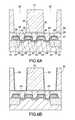
- FIG. 11A and FIG. 11Bwe will describe the configuration of the stacked-type capacitor having the conventional high dielectric constant film.
- FIG. 11Athere is shown a schematic plan view of the stacked-type capacitor only with a lower electrode 105 , a capacity insulator film 106 , and an upper electrode 107 for simplified illustration.
- FIG. 11Bis a cross sectional view of the stacked-type capacitor along the break line X-Y in FIG. 11A.
- a diffusion layer 102 with a N-type electric conductionis formed on a predetermined area of the surface of a silicon substrate 101 with a P-type electric conduction.
- a part of an insulator film 103 on the silicon substrate 101is opened and filled with a plug 104 .
- the lower electrode 105is formed on the insulator film 105 so as to directly cover the insulator film 105 .
- the lower electrode 105can be electrically connected to the diffusion layer 102 through the plug 104 .
- the capacity insulator film 106is formed on the side and top of the lower electrode 105 and the exposed surface of the interlayer insulator film 103 .
- the insulator film 106is made of a metal film such as a ruthenium oxide film, while the capacity insulator film 106 is made of another metal film such as a Ta 2 O 5 film or a STO film.
- an upper electrode 107is formed so as to cover the whole.
- the upper electrode 107may be made of the same material as that of the lower electrode 105 .
- the present inventorshave been thoroughly studied about the capacitor having a Metal/Insulator/Metal (MIM) structure in which a high dielectric constant material such as one described above is used as a capacity insulator film. Consequently, they found the fact that a leak current in the capacity insulator film increased as the measuring temperature increased when the capacity insulator film was made of a metal oxide film such as a tantalum pentoxide (Ta 2 0 5 ), zirconium dioxide (ZrO 2 ), hafnium dioxide (HfO 2 ), STO(SrTiO 3 ), BST((Ba,Sr) TiO 3 ), orPZT(Pb(Zr,Ti) 0 3 ) film.
- a metal oxide filmsuch as a tantalum pentoxide (Ta 2 0 5 ), zirconium dioxide (ZrO 2 ), hafnium dioxide (HfO 2 ), STO(SrTiO 3 ), BST((Ba,S
- FIG. 12there is shown one of the features of a capacitor having the above MIM structure (hereinafter, simply referred to as a MIM capacitor) in which a STO film is used as its capacity insulator film.
- a MIM capacitorin which a STO film is used as its capacity insulator film.
- the applied voltage between the lower electrode and the upper electrodeis in the range of ⁇ 1 volt to +1 volt.
- the horizontal axisrepresents the inverse (1/T) of an absolute temperature (i.e., a measuring temperature measured in kelvins (K)), while the vertical axis represents the logarithm of leak current (J/T 2 ) in the capacitor (insulator) film.
- the leak current (J/T 2 ) in the capacitoris substantially in inverse proportion to the inverse (1/T) of the measuring temperature.
- the leak (J/T 2 ) in the capacitorcan be restricted with the thermal release of electrons from the lower or upper electrode (i.e., the capacitor electrode) to the capacitive insulator film.
- the leak current (J) in the capacitor filmdramatically increases as the measuring temperature increases.
- the dependence of such a leak current on temperatureis varied with respect to the above applied voltage. Whatever the case may be, however, the leak current is proportional to the measuring temperature.
- a guaranteed operating temperature of the semiconductor deviceshould be of about 150° C. at maximum.
- the increase in leak currentstrongly affects on the operation of the device.
- the MIM capacitorthere is a growing demand on the MIM capacitor in that its capacity insulator film must be prevented from the increase in leak current even though the operation temperature increases.
- An object of the present inventionis to provide a method for fabricating a semiconductor device where the capacitance value of a capacity insulator film made of a metal oxide having a high dielectric constant is increased by a simple procedure.
- a method for fabricating a semiconductor devicecomprising the steps of: forming a metal film as a lower electrode of a capacitor on a semiconductor substrate, followed by forming a capacity insulator film over the lower electrode by means of atomic layer chemical vapor deposition (ALCVD); and forming an upper electrode of the capacitor on the capacity insulator film.
- ACVDatomic layer chemical vapor deposition
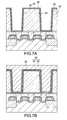
- FIG. 1Ais a plan view of the MIM capacitor for illustrating the first embodiment of the present invention
- FIG. 1Bis a cross sectional view of the MIM capacitor along the break line A-B in FIG. 1A;
- FIGS. 2A and 2Bare cross sectional views of enlarged parts of the MIM capacitor shown in FIG. 1A, respectively;
- FIGS. 3A and 3Bare cross sectional views of enlarged parts of another MIM-structured capacitor, respectively;
- FIG. 4Ais a cross sectional view of the capacitor for illustrating the step of forming the capacity insulator film in accordance with the present invention
- FIG. 4Bis a sequence diagram for introducing the reaction gases into the reaction chamber for the ALCVD process
- FIG. 5Ais a cross sectional view of the capacitor for illustrating the step of forming the capacity insulator film in accordance with the present invention
- FIG. 5Bis a sequence diagram for introducing the reaction gases into the reaction chamber for the ALCVD process
- FIG. 6A and 6Bare cross sectional views for illustrating different steps for fabricating the MIM capacitor in accordance with the second embodiment of the present invention, respectively;
- FIG. 7A and 7Bare cross sectional views for illustrating further steps for fabricating the MIM capacitor in accordance with the second embodiment of the present invention, respectively;
- FIG. 8is a graph for explaining the effects of the present invention.
- FIG. 9is a cross sectional view of the conventional MIM-structured capacitor for contrasting with the second embodiment of the present invention.
- FIG. 10is a graph for illustrating the generation of leak current in the capacity insulator film of the conventional MIM-structured capacitor
- FIG. 11Ais a plan view of the conventional MIM-structured capacitor and FIG. 11B is a cross sectional view thereof along the break line X-Y in FIG. 11A;
- FIG. 12is a graph for explaining the problems of the prior art, in which the measuring temperature dependency of leak current in the capacitor film is illustrated.
- FIG. 1A and FIG. 1Bthere is shown a capacitor for illustrating a method for fabricating a semiconductor device as a first preferred embodiment of the present invention.
- the capacitor to be implemented on a semiconductor deviceis fabricated as follows. First, a silicon substrate 1 with a P-type electric conduction is prepared and a diffusion layer 2 with a N-type electric conduction is then formed on a predetermined area of the surface of the silicon substrate 1 . Subsequently, an interlayer insulator film 3 is formed on both the silicon substrate 1 and the diffusion layer 2 .
- a plug 4is formed by making a hole through a part of an interlayer insulator film 3 so as to extend on the surface of the N-type diffusion layer 2 , followed by forming a lower electrode 5 so as to directly cover the surface of the interlayer insulator film 3 and to make an electrical contact with the diffusion layer 2 through the plug 4 .
- the interlayer insulator film 3consists of a silicon oxide film
- the plug 4consists of a barrier film made of titanium nitride (Tin) with tungsten.
- the lower electrode 5consists of a metal film made of ruthenium dioxide.
- the capacitor of the present embodimentincludes first and second dielectric films.
- the first dielectric filmis prepared by covering the surface of the interlayer insulator film 3 and the surface of the lower electrode 5 with an extra-thin barrier insulator layer 6 .
- the barrier insulator layer 6is an alumina film with a thickness of from 1 nm to 5 nm.
- the relative dielectric constant of such an alumina filmis on the order of 10. In this case, the current passing through the film is Fowler Nordheim (F-N) tunneling current or direct tunneling current mechanism.
- F-NFowler Nordheim
- a high dielectric constant film 7is provided as the second dielectric film and covers the surface of the barrier insulator layer 6 .
- the high dielectric constant film 7is made of tantalum pentoxide (Ta 2 O 5 ) with a film thickness of about 10 nm.
- the Ta 2 O 5 filmhas a relative dielectric constant of about 25.
- the barrier insulator layer 6 and the high dielectric constant film 7make up a capacity insulator film 8 .
- an upper electrode 7is formed so as to cover the whole of the above structure in fabrication.
- the upper electrode 7consists of a metal film made of tungsten or the like.
- the MIM capacitorcan be fabricated by the above steps in the method of the present embodiment.
- FIG. 2Ais an enlarged cross sectional view of a portion circled by the break line 10 in FIG. 1B and FIG. 2B is an enlarged cross sectional view of a portion circled by the break line 11 in FIG. 1 B.
- the barrier insulator layer 6 and the high dielectric constant film 7are successively formed on the lower electrode 5 , and the upper electrode 9 is then formed on the surface of the high dielectric constant film 7 .
- the lower electrode 5 and the upper electrode 9are metal films as described above.
- the lower electrodeis the RuO 2 film as described above.
- the lower electrodemay be one selected from an IrO 2 film, a RuO 2 /Ru film (i.e., a laminated film where a Ruo 2 film is deposited on a Ru film), and an IrO 2 /Ir film (i.e., a laminated film where an IrO 2 film is deposited on an Ir film) .
- the lower electrode 5may be a TiN film, a TaN film, or a WN film, or alternatively a metal film coated with a TiN film or a TaN film.
- the upper electrode 9may be prepared from a metal with a high melting point, such as tungsten, in stead of the above metal film.
- the barrier insulator layer 6is an insulator film having the F-N tunneling current or direct tunneling current mechanism.
- a laminated film 6may be a siliconoxinitride (SION) film. That is, the material to be used is one that brings the barrier insulator layer 6 into intimate contact with the above lower electrode 5 .
- the high dielectric constant film 7may be a metal oxide film such as a zirconium dioxide (ZrO 2 ) film, a hafnium dioxide (HfO 2 ) film, a STO (SrTiO 3 ) film, BST ((Ba, Sr)TiO 3 ) film, or a PZT (Pb (Zr, Ti)O 3 ) film.
- a metal oxide filmsuch as a zirconium dioxide (ZrO 2 ) film, a hafnium dioxide (HfO 2 ) film, a STO (SrTiO 3 ) film, BST ((Ba, Sr)TiO 3 ) film, or a PZT (Pb (Zr, Ti)O 3 ) film.
- the inter layer insulator film 3may be an insulator film based on a Si—O bond.
- Such an insulator filmmay be a low dielectric constant film made of a compound selected from silsesquionxanes including hydrogen silsesquioxane, methyl silsesquioxane, methylated hydrogen silsequioxane, and furuorinated silsesquioxane.
- the barrier insulator layer 6is made of a material that facilitates the cladding to the interlayer insulator film 3 .
- the cladding of the above alumina film to the above interlayer insulator filmcan be very strong.
- FIG. 3we will describe another configuration of the capacity insulator film in accordance with the present invention.
- FIGS. 3A and 3Bare enlarged cross sectional views of the MIM capacitor shown in FIGS. 1A and 1B, as in the cases of FIGS. 2A and 2B.
- the high dielectric constant film 7is formed and coated on the surface of the lower electrode 5 and then a barrier insulator layer 6 a is formed on the surface of the high dielectric constant film, followed by forming the upper electrode 9 on the barrier insulator layer 6 a.
- FIG. 3Athe high dielectric constant film 7 is formed and coated on the surface of the lower electrode 5 and then a barrier insulator layer 6 a is formed on the surface of the high dielectric constant film, followed by forming the upper electrode 9 on the barrier insulator layer 6 a.
- the barrier insulator film 6is formed and coated on the surface of the lower electrode 5 and then the high dielectric constant film and the laminated film 6 a are successively formed on the barrier insulator film 6 , followed by forming the upper electrode 9 on the laminated film 6 a.
- each of the lower electrode 5 , the barrier insulator films 6 , 6 a, the high dielectric constant film 7 , and the upper electrode 9may be the same material as one explained in the description for FIG. 2A.
- FIGS. 4A and 4B and FIGS. 5A and 5Bwe will describe the method for preparing the laminated film 6 and the high dielectric constant film 7 which serve as the building blocks for the MIM capacitor shown in FIGS. 1A and 1B.
- FIG. 4Ais a cross sectional view of the structure after forming the barrier insulator film 6 on both the surface of the interlayer insulator film 3 and the surface of the lower electrode 5 .
- a barrier insulator film 6is prepared by means of the atomic layer chemical vapor deposition (ALCVD) (hereinafter, simply referred to as the ALCVD process)
- a system to be used in this casemay be a multiple chamber film formation system.
- the film formation in the ALCVD processis performed by introducing reaction gases into reaction chambers intermittently as precisely spaced pulses.
- the sequence of introducing the reaction gases into the chamberis illustrated in FIG. 4B.
- a semiconductor wafer to be subjected to the film formationis placed on a substrate at a temperature in the range of 200° C. to 350° C. in the chamber.
- an atmospheric gas to be introduced into the chamberis an inert gas such as a nitrogen gas or an argon gas and the gas pressure in the chamber is kept at the order of 100 Pa.
- a trimethyl aluminum gasis introduced into the chamber intermittently as precisely spaced pulses.
- the intermittently spaced introduction of the TMA gasallows the chemical adsorption of TMA or its activated species on both the surface of the interlayer insulator film 3 and the surface of the lower electrode 5 . In this embodiment, such a chemical adsorption forms a single atomic layer.
- the lower electrode 5should be a conductive metal film made of metal oxide or metal nitride as illustrated in FIG. 2A.
- the interlayer insulator film 3is an insulator film provided as a silicon oxide film, so that TMA can be easily accumulated on the surface of such a film by means of chemical adsorption.
- the introduction of TMA gasis interrupted and a purge gas is then introduced into the chamber as a pulse to exhaust the TMA gas from the chamber.
- the purge gasmay be a nitrogen gas, an argon gas, a helium gas.
- the introduction of purge gasis interrupted and an oxidation gas is then introduced into the chamber as a pulse.
- the oxidation gasthermally reacts with the TMA or activated species thereof adsorbed on both the surface of the interlayer insulator film 3 and the surface of the lower electrode 5 , resulting in the formation of an alumina film at an atomic layer level.
- the oxidation gasmay be ozone ( 0 3 ).
- the purge gasis introduced into the chamber again as a pulse.
- the adsorption of TMA or activated species thereof and the oxidation of adsorbed TMA or activated species thereofare provided as events in a unit cycle for forming the alumina film at an atomic layer level.
- a unit cycleis repeatedly performed to adjust the film thickness of the barrier insulator layer 6 .
- the unit cycleis completed within about one second and the film thickness of the alumina film at the atomic layer level may be in the range of 0.1 nm to 0.2 nm.
- the unit cyclecan be repeated ten or twenty times.
- the alumina film with a film thickness of 1 nm to 5 nmis formed and provided as a barrier insulator film 6 .
- the temperature of the substrate in the ALCVD processmay be adjusted at 400° C. or less.
- barrier insulator layer 6having the exceedingly high coating property to both the surface of the interlayer 6 and the surface of the lower electrode 5 in the ALCVD process.
- FIG. 5Ais a cross sectional view of the structure after forming the high dielectric constant film 7 so as to be coated on the surface of the interlayer insulator film 3 and the surface of the barrier insulator layer 6 on the lower electrode 5 .
- reaction gasesare introduced into another chamber of the above multi-chamber film formation system intermittently as spaced pulses.
- FIG. 5Billustrates the sequence of introducing such reaction gases into the reaction chamber.
- a semiconductor wafer to be subjected to the film formationis placed on the substrate at a temperature in the range of 200° C. to 350° C. in the above chamber.
- an atmospheric gasis introduced into the reaction chamber and the gas pressure in the chamber is kept at the order of 200 Pa.
- a tantalum tetrachloride (TaCl 4 ) gasis introduced as a source gas into the chamber as intermittently as spaced pulses.
- TaCl 4tantalum tetrachloride
- Such intermittently spaced introduction of such a source gasallows the chemical adsorption of Ta atoms or tantalum chloride on the surface of the barrier insulator layer 5 .
- such a chemical adsorptionis of a single atomic layer or of several atomic layers.
- the Ta atomscombine with oxygen atoms, so that they can be chemically adsorbed on the surface of the barrier insulator layer 6 without any difficulty.
- a purge gasis introduced into the chamber as a pulse when the introduction of source gas is interrupted to exhaust the source gas from the chamber.
- an oxidation gasis introduced into the chamber as a pulse during the period of interrupting the introduction of purge gas.
- the oxidation gasthermally reacts with the adsorbed Ta atoms to form a tantalum pentoxide film at an atomic layer level.
- the oxidation gasmaybe water vapor (H 2 O), ozone (O 3 ), or the like.
- the purge gasis introduced into the chamber again.
- the adsorption of Ta atoms and the oxidation of adsorbed Ta atomsare provided as events in a unit cycle for forming the tantalum pentoxide film at an atomic layer level or at several layer levels.
- a cycleis repeatedly performed to adjust the film thickness of the high dielectric constant film 7 .
- the rate of forming such a tantalum pentoxide filmis on the order of 5 nm/minute. Therefore, the tantalum pentoxide film of 10 nm in film thickness can be obtained within the order of 2 minutes.
- each of the barrier insulator layer 6 and the high dielectric constant film 7can be controlled more effectively if each of them is formed by the above ALCVD process.
- the ALCVD processallows the extensive improvement on the step coverage characteristics of the capacity insulator film (i.e., the capability of covering the stepped portion to be caused in the film formation). Therefore, the high-quality capacity insulator film having excellent insulation performance can be easily formed.
- the problem of oxygen depletioncan be solved when the high dielectric constant film is formed by such a process, so that the subsequent step of heat treatment on the high dielectric constant film in an atmosphere of oxygen can be eliminated.
- the above advantages of using the ALCVD processis not limited to the case in which the tantalum pentoxide film is provided as the high dielectric constant film. Such advantages can be also obtained using the metal oxide film explained in the description for FIG. 2.
- FIGS. 6A and 6B and FIGS. 7A and 7BA second preferred embodiment of the present invention will be now described in detail with reference to FIGS. 6A and 6B and FIGS. 7A and 7B.
- a MIM-structured capacitoris formed on a logic device to be fabricated with 0.10- ⁇ m design rules. The effects to be caused as a result of leak current in the capacity insulator film in the capacitor of the present embodiment will be concretely described below.
- a chip separation area 22is formed on a silicon substrate 21 with a P-type electric conduction by the process of shallow trench isolation (STI). Then, a polycrystal silicon layer 23 is formed on the silicon substrate 21 through a gate insulator film and then a side-wall insulator film 24 is formed on the side wall of the polycrystal silicon layer 23 by the well known process in the art.
- STIshallow trench isolation
- a source drain diffusion layer 25 with a N-type electric conductionis formed by means of ion implantation and thermal treatment. Furthermore, using the silicide technology, a silicide layer 26 is selectively formed on the surface of the polycrystal silicon layer 23 and the surface of the source drain diffusion layer 25 . In this embodiment, the silicide layer 26 can be made of cobalt silicide.
- a protective insulator film 27is formed using a silicon nitride film, followed by depositing a silicon oxide film thereon to form a first interlayer insulator film 28 . Subsequently, a predetermined area of the first interlayer insulator film 28 is opened to form a hole to be filled with a plug 29 .
- the plug 29consists of tungsten.
- a etching stopper layer 30 and a second interlayer insulator film 31are laminated on the surface of the first interlayer insulator film 28 and the top of the plug 29 .
- the etching stopper 30is a thin silicon nitride film and the second interlayer insulator film 31 is a silicon oxide film.
- the predetermined area of the second interlayer insulator film 31is subjected to a reactive ion beam etching (RIE) to perform dry etching to form a capacitance hole 32 .
- RIEreactive ion beam etching
- the etching stopper layer 30protects the plug 29 from the dry etching in the RIE process.
- the subsequent dry etchingallows the selective removal of the etching stopper layer 30 to complete the formation of such a hole 32 .
- a lower electrode 33is formed along the inner side of the capacitance hole 32 .
- the lower electrode 33is connected to the plug 29 .
- the lower electrode 33consists of a TiN film with a film thickness of about 20 nm.
- a barrier insulator layer 34is formed on the surface of the high lower electrode 33 and the surface of the second interlayer insulator film 31 by depositing an alumina film of 2 nm in film thickness. Then, a high dielectric constant film 35 is formed on the barrier insulator layer 34 by depositing a tantalum pentoxide film of 10 nm in film thickness.
- a barrier conductive layer 36 and a tungsten film 37are successively formed on the high dielectric constant film 35 and are then subjected to the step of pattering using the well known photolithographic and dry etching technologies to make an upper electrode 38 , resulting in a basic structure of the MIM capacitor.
- the obtained resultsare represented as a graph shown in FIG. 8. In this figure, the potentials applied between the lower electrode 33 and the upper electrode 38 are plotted on the horizontal axis. To be more specific, the source drain diffusion layer 25 and the silicon substrate 21 are grounded and positive or negative potential is applied on the upper electrode 38 .
- the leak currents in the capacity (insulator) filmare plotted on the vertical axis of the graph.
- a set of the measuring temperatures 25° C. (room temp.), 85° C., and 125° C.is used as the parameter as shown in the figure.
- the leak currents in the capacity filmdo not depend on the measuring temperatures at all. It means that the current passing through the barrier insulator layer 34 has nothing to do with the dependency on temperature. In this embodiment, the flow of electrons in the barrier insulator layer 34 may become Fowler Nordheim (F-N) tunneling current or direct tunneling current mechanism.
- F-NFowler Nordheim
- FIG. 9is identical to the second preferred embodiment except that a high dielectric constant film 35 formed on the lower electrode 33 is made of a tantalum pentoxide film with a film thickness of 10 nm.
- an upper electrode 38is comprised of a barrier conductive layer 36 and a tungsten film 37 and placed on the high dielectric constant film 35 .
- the second embodimenthas been explained for the capacitor in which the barrier insulator layer 34 is formed on the surface of the lower electrode 33 .
- itis not limited to such a configuration.
- the dependency of leak current in the capacity insulator film on temperaturecannot be observed in each of the designs in which the barrier insulator layer is placed between the high dielectric constant film and the upper electrode, or the barrier insulator layers are respectively placed between the lower electrode and the high dielectric constant film and between the upper electrode and the high dielectric constant film.
- a metal film to be used as the lower or upper electrodemay be osmium (Os) or oxide thereof, rhenium (Re), platinum (Pt), palladium (Pd), or rhodium (Rh) .
- rhenium (Re)platinum
- Ptpalladium
- Rhrhodium
- a metal filmmay be titanium (Ti), tantalum (Ta), ruthenium (Ru), or iridium (Ir).
- any conductive compoundmay be used, such as the above metal oxide or the metal nitride, oxynitride, or carbide.
- the metal film that makes up the lower or upper electrodemay be provided as a laminated material consisting of different metal films.
- the alumina film or SiON filmhas been explained as the barrier insulator layer.
- the barrier insulator filmmay be any insulator film having the F-N tunneling current or direct tunneling current mechanism.
- the tantalum pentoxide filmis formed by the ALCVD process.
- the respective source gas as shown in FIG. 5Bmaybe alcoholate, hafnium chloride, strontiumDRM, barium DRM, or titanium chloride.
- the approximate relative dielectric constant of the above high dielectric constant filmis 25 for the zirconium dioxide (ZrO 2 ), 30 for the relative dielectric constant of the hafnium dioxide (HfO 2 ) film, 100 for the STO (SrTiO 3 ) film, and 300 for the BST ((Ba, Sr) TiO 3 ) film.
- the temperature for film formationmay be in the range of 200° C. to 350° C.
- the metal oxide film as described aboveis prepared by the above ALCVD process, such a film can be used as a capacityin sulator film of the MIM capacitor.
- a metal oxide filmmay be provided by stacking the different metal oxide films.
- the MIM capacitor using a high dielectric constant material such as a metal oxide film as a capacity insulator filman insulator film is provided as a barrier insulator layer between a lower electrode or an upper electrode and the high dielectric constant material of the capacitor, where the flow of electrons in the insulator film becomes Fowler Nordheim (F-N) tunneling current or direct tunneling current mechanism.
- the barrier insulator film or the capacity insulator filmmay be formed by the ALCVD process.
- the composition of the capacity insulator filmcan be controlled more effectively as it is formed by the above ALCVD process.
- the ALCVD processallows the extensive improvement on the step coverage characteristics of the capacity insulator film (i.e., the capability of covering the stepped portion to be caused in the film formation). Therefore, the high-quality capacity insulator film having excellent insulation performance and the negligible dependency of its operation on temperature can be easily formed.
- the operation of the semiconductor device on which the MIM capacitor is mountedbecomes very stable.
- the stacked type capacitor having the high reliability, in which the high dielectric constant film is used as a capacity insulator film,can be obtained, so that the very high integration and high densification of semiconductor device can be extensively accelerated.
Landscapes
- Engineering & Computer Science (AREA)
- Manufacturing & Machinery (AREA)
- Physics & Mathematics (AREA)
- Condensed Matter Physics & Semiconductors (AREA)
- General Physics & Mathematics (AREA)
- Computer Hardware Design (AREA)
- Microelectronics & Electronic Packaging (AREA)
- Power Engineering (AREA)
- Chemical & Material Sciences (AREA)
- Chemical Kinetics & Catalysis (AREA)
- Materials Engineering (AREA)
- Semiconductor Memories (AREA)
- Semiconductor Integrated Circuits (AREA)
Abstract
Description
- 1. Field of the Invention[0001]
- The present invention relates to a method for fabricating a semiconductor device, especially a method for forming a capacitor structure in the semiconductor device.[0002]
- 2. Description of the Prior Art[0003]
- Among various types of semiconductor device, dynamic RAMs (DRAMs) have been well known in the art as memory devices where the input and output of information can be performed as needed. A typical memory cell of such a DRAM is structurally simple and comprises two components: a transfer transistor and a capacitor. Therefore, it is applied very extensively in various fields because of such a simple circuitry most suitable for providing a highly integrated semiconductor device.[0004]
- Also, in the latest technology of semiconductor device, system LSIs are becoming important. For providing such semiconductor devices, various mixed semiconductor devices with fundamentally different types of components have been developed and studied, such as a logic-mixed memory device in which a logic circuit and a memory circuit are mounted together on a single semiconductor chip and an analog-mixed logic device in which a logic circuit and an analog circuit are mounted on a single semiconductor chip Just as in the case with the DRAM mentioned above, the mixed semiconductor device has a memory cell consisting of a transfer transistor and a capacitor.[0005]
- In conjunction with the further increase in integration of semiconductor device, a capacitor having a three-dimensional structure has been developed and used for that memory cell. The reason of fabricating the three-dimensionally structured capacitor is the follow. That is, in connection with the fabrication of finer and denser semiconductor device, the reduction in the occupied area of a capacitor becomes indispensable. In this case, however, the capacity of the capacitor should be kept at more than the predetermined level for ensuring the reliable and stable operation of a memory part of the semiconductor device. Therefore, it becomes indispensable to change the shape of each electrode in the capacitor from a flat shape into a three-dimensional shape so as to expand the surface area of the electrode in its reduced area occupied in the capacitor.[0006]
- For such a three-dimensional structure of the capacitor in the memory cell, there are two structural designs (i.e., a stack structure and a trench structure). Each of these structures has its own merits and demerits. The stack structure has considerable tolerance to an incident alpha-ray or a noise from any circuit or the like, allowing the operation of the capacitor in stable even at a comparatively small capacitance value. Therefore, such a stack structure may be effective in the process of fabricating a semiconductor device even though the chip employs design rules of approximately 0.10 μm.[0007]
- Recently, furthermore, the capacitor having the stack structure (hereinafter, such a capacitor is referred to as a stacked-type capacitor) requires a dielectric film (i.e., a capacity insulator film) with an extremely high dielectric constant for ensuring a predetermined capacitance value in a very small area. Therefore, several materials have been intensively studied for the dielectric film. The materials include insulating materials such as tantalum pentoxide (Ta[0008]2O5), SrTiO3(hereinafter, simply referred to as a STO), a (Ba, Sr)TiO3(hereinafter, simply referred to as a BST), and Pb(Zr, Ti)03(hereinafter, simply referred to as a PZT). Moreover, it becomes necessary to provide a new conductive material to be provided as a lower electrode of the above stacked-type capacitor for the purpose of ensuring a high reliability of the capacitor by means of an appropriate combination of the above high dielectric insulator material with the lower electrode. In the Digest of Technical Papers, pp. 831-834, of the annual IEEE International Electron Devices Meeting (IEDM) held on 1994, a STO film is used as a capacity insulator film and ruthenium dioxide (RuO2) is used as a conductive material of a lower electrode. In addition, the same kind of the capacitor structure can be found in Japanese Patent Application Laying-open No. 2000-114482.
- Referring now to FIG. 11A and FIG. 11B, we will describe the configuration of the stacked-type capacitor having the conventional high dielectric constant film. In FIG. 11A, there is shown a schematic plan view of the stacked-type capacitor only with a[0009]
lower electrode 105, acapacity insulator film 106, and anupper electrode 107 for simplified illustration. FIG. 11B is a cross sectional view of the stacked-type capacitor along the break line X-Y in FIG. 11A. - As shown in FIG. 11B, a[0010]
diffusion layer 102 with a N-type electric conduction is formed on a predetermined area of the surface of asilicon substrate 101 with a P-type electric conduction. A part of aninsulator film 103 on thesilicon substrate 101 is opened and filled with aplug 104. Also, thelower electrode 105 is formed on theinsulator film 105 so as to directly cover theinsulator film 105. Thus, thelower electrode 105 can be electrically connected to thediffusion layer 102 through theplug 104. - As shown in FIG. 11A and FIG. 11B, furthermore, the[0011]
capacity insulator film 106 is formed on the side and top of thelower electrode 105 and the exposed surface of theinterlayer insulator film 103. Here, theinsulator film 106 is made of a metal film such as a ruthenium oxide film, while thecapacity insulator film 106 is made of another metal film such as a Ta2O5film or a STO film. Then, anupper electrode 107 is formed so as to cover the whole. Here, theupper electrode 107 may be made of the same material as that of thelower electrode 105. - The present inventors have been thoroughly studied about the capacitor having a Metal/Insulator/Metal (MIM) structure in which a high dielectric constant material such as one described above is used as a capacity insulator film. Consequently, they found the fact that a leak current in the capacity insulator film increased as the measuring temperature increased when the capacity insulator film was made of a metal oxide film such as a tantalum pentoxide (Ta[0012]205), zirconium dioxide (ZrO2), hafnium dioxide (HfO2), STO(SrTiO3), BST((Ba,Sr) TiO3), orPZT(Pb(Zr,Ti)03) film.
- In the following description, we will give a brief explanation of the dependence of the above leak current on measuring temperature with reference to FIG. 12. In this figure, there is shown one of the features of a capacitor having the above MIM structure (hereinafter, simply referred to as a MIM capacitor) in which a STO film is used as its capacity insulator film. In this case, furthermore, the applied voltage between the lower electrode and the upper electrode is in the range of −1 volt to +1 volt.[0013]
- In the graph shown in FIG. 12, the horizontal axis represents the inverse (1/T) of an absolute temperature (i.e., a measuring temperature measured in kelvins (K)), while the vertical axis represents the logarithm of leak current (J/T[0014]2) in the capacitor (insulator) film. As shown in FIG. 12, the leak current (J/T2) in the capacitor is substantially in inverse proportion to the inverse (1/T) of the measuring temperature. In other words, the leak (J/T2) in the capacitor can be restricted with the thermal release of electrons from the lower or upper electrode (i.e., the capacitor electrode) to the capacitive insulator film. In the prior art, therefore, the leak current (J) in the capacitor film dramatically increases as the measuring temperature increases. By the way, it is also known that the dependence of such a leak current on temperature is varied with respect to the above applied voltage. Whatever the case may be, however, the leak current is proportional to the measuring temperature.
- For operating the semiconductor device, a guaranteed operating temperature of the semiconductor device should be of about 150° C. at maximum. Notably in the case of the logic mixed memory device, the increase in leak current strongly affects on the operation of the device. For such a logic mixed memory device, therefore, there is a growing demand on the MIM capacitor in that its capacity insulator film must be prevented from the increase in leak current even though the operation temperature increases.[0015]
- An object of the present invention is to provide a method for fabricating a semiconductor device where the capacitance value of a capacity insulator film made of a metal oxide having a high dielectric constant is increased by a simple procedure.[0016]
- There is provided a method for fabricating a semiconductor device, comprising the steps of: forming a metal film as a lower electrode of a capacitor on a semiconductor substrate, followed by forming a capacity insulator film over the lower electrode by means of atomic layer chemical vapor deposition (ALCVD); and forming an upper electrode of the capacitor on the capacity insulator film.[0017]
- The above mentioned and other objects, features and advantages of this invention will become more apparent by reference to the following detailed description of the invention taken in conjunction with the accompanying drawings, wherein:[0018]
- FIG. 1A is a plan view of the MIM capacitor for illustrating the first embodiment of the present invention, and FIG. 1B is a cross sectional view of the MIM capacitor along the break line A-B in FIG. 1A;[0019]
- FIGS. 2A and 2B are cross sectional views of enlarged parts of the MIM capacitor shown in FIG. 1A, respectively;[0020]
- FIGS. 3A and 3B are cross sectional views of enlarged parts of another MIM-structured capacitor, respectively;[0021]
- FIG. 4A is a cross sectional view of the capacitor for illustrating the step of forming the capacity insulator film in accordance with the present invention, and FIG. 4B is a sequence diagram for introducing the reaction gases into the reaction chamber for the ALCVD process;[0022]
- FIG. 5A is a cross sectional view of the capacitor for illustrating the step of forming the capacity insulator film in accordance with the present invention, and FIG. 5B is a sequence diagram for introducing the reaction gases into the reaction chamber for the ALCVD process;[0023]
- FIG. 6A and 6B are cross sectional views for illustrating different steps for fabricating the MIM capacitor in accordance with the second embodiment of the present invention, respectively;[0024]
- FIG. 7A and 7B are cross sectional views for illustrating further steps for fabricating the MIM capacitor in accordance with the second embodiment of the present invention, respectively;[0025]
- FIG. 8 is a graph for explaining the effects of the present invention;[0026]
- FIG. 9 is a cross sectional view of the conventional MIM-structured capacitor for contrasting with the second embodiment of the present invention;[0027]
- FIG. 10 is a graph for illustrating the generation of leak current in the capacity insulator film of the conventional MIM-structured capacitor;[0028]
- FIG. 11A is a plan view of the conventional MIM-structured capacitor and FIG. 11B is a cross sectional view thereof along the break line X-Y in FIG. 11A; and[0029]
- FIG. 12 is a graph for explaining the problems of the prior art, in which the measuring temperature dependency of leak current in the capacitor film is illustrated.[0030]
- Hereinafter, we will describe preferred embodiments of the present invention in detail with reference to the attached drawings.[0031]
- (First Preferred Embodiment)[0032]
- Referring to FIG. 1A and FIG. 1B, there is shown a capacitor for illustrating a method for fabricating a semiconductor device as a first preferred embodiment of the present invention. As with the conventional one shown in FIG. 11A and FIG. 11B, the capacitor to be implemented on a semiconductor device is fabricated as follows. First, a[0033]
silicon substrate 1 with a P-type electric conduction is prepared and adiffusion layer 2 with a N-type electric conduction is then formed on a predetermined area of the surface of thesilicon substrate 1. Subsequently, aninterlayer insulator film 3 is formed on both thesilicon substrate 1 and thediffusion layer 2. Then, aplug 4 is formed by making a hole through a part of aninterlayer insulator film 3 so as to extend on the surface of the N-type diffusion layer 2, followed by forming alower electrode 5 so as to directly cover the surface of theinterlayer insulator film 3 and to make an electrical contact with thediffusion layer 2 through theplug 4. In this embodiment, theinterlayer insulator film 3 consists of a silicon oxide film, and theplug 4 consists of a barrier film made of titanium nitride (Tin) with tungsten. Also, thelower electrode 5 consists of a metal film made of ruthenium dioxide. - Furthermore, the capacitor of the present embodiment includes first and second dielectric films. The first dielectric film is prepared by covering the surface of the[0034]
interlayer insulator film 3 and the surface of thelower electrode 5 with an extra-thinbarrier insulator layer 6. Here, thebarrier insulator layer 6 is an alumina film with a thickness of from 1 nm to 5 nm. Also, the relative dielectric constant of such an alumina film is on the order of 10. In this case, the current passing through the film is Fowler Nordheim (F-N) tunneling current or direct tunneling current mechanism. Subsequently, a high dielectricconstant film 7 is provided as the second dielectric film and covers the surface of thebarrier insulator layer 6. Here, the high dielectricconstant film 7 is made of tantalum pentoxide (Ta2O5) with a film thickness of about 10 nm. In addition, the Ta2O5film has a relative dielectric constant of about 25. As shown in the figures, thebarrier insulator layer 6 and the high dielectricconstant film 7 make up acapacity insulator film 8. - Moreover, an[0035]
upper electrode 7 is formed so as to cover the whole of the above structure in fabrication. Here, theupper electrode 7 consists of a metal film made of tungsten or the like. - Accordingly, the MIM capacitor can be fabricated by the above steps in the method of the present embodiment.[0036]
- Referring now to FIG. 2A and FIG. 2A, the features of the present embodiment will be further described in detail. FIG. 2A is an enlarged cross sectional view of a portion circled by the[0037]
break line 10 in FIG. 1B and FIG. 2B is an enlarged cross sectional view of a portion circled by the break line11 in FIG.1B. - As shown in FIG. 2A, the[0038]
barrier insulator layer 6 and the high dielectricconstant film 7 are successively formed on thelower electrode 5, and theupper electrode 9 is then formed on the surface of the high dielectricconstant film 7. Here, thelower electrode 5 and theupper electrode 9 are metal films as described above. In addition, the lower electrode is the RuO2film as described above. In this embodiment, alternatively, the lower electrode may be one selected from an IrO2film, a RuO2/Ru film (i.e., a laminated film where a Ruo2film is deposited on a Ru film), and an IrO2/Ir film (i.e., a laminated film where an IrO2film is deposited on an Ir film) . Furthermore, thelower electrode 5 may be a TiN film, a TaN film, or a WN film, or alternatively a metal film coated with a TiN film or a TaN film. In this embodiment, furthermore, theupper electrode 9 may be prepared from a metal with a high melting point, such as tungsten, in stead of the above metal film. - As described above, the[0039]
barrier insulator layer 6 is an insulator film having the F-N tunneling current or direct tunneling current mechanism. Such alaminated film 6 may be a siliconoxinitride (SION) film. That is, the material to be used is one that brings thebarrier insulator layer 6 into intimate contact with the abovelower electrode 5. - In stead of the Ta[0040]2O5film, furthermore, the high dielectric
constant film 7 may be a metal oxide film such as a zirconium dioxide (ZrO2) film, a hafnium dioxide (HfO2) film, a STO (SrTiO3) film, BST ((Ba, Sr)TiO3) film, or a PZT (Pb (Zr, Ti)O3) film. - As shown in FIG. 2B, furthermore, the[0041]
barrier insulator layer 6 and the high dielectricconstant film 7 are laminated on theinterlayer insulator film 3, followed by forming theupper electrode 9 on the surface of the high dielectricconstant film 7. Instead of the silicon dioxide film, the interlayer insulator film 3 may be an insulator film based on a Si—O bond. Such an insulator film may be a low dielectric constant film made of a compound selected from silsesquionxanes including hydrogen silsesquioxane, methyl silsesquioxane, methylated hydrogen silsequioxane, and furuorinated silsesquioxane. - In this embodiment, a matter of great import is that the[0042]
barrier insulator layer 6 is made of a material that facilitates the cladding to theinterlayer insulator film 3. Thus, the cladding of the above alumina film to the above interlayer insulator film can be very strong. - Referring now to FIG. 3, we will describe another configuration of the capacity insulator film in accordance with the present invention.[0043]
- FIGS. 3A and 3B are enlarged cross sectional views of the MIM capacitor shown in FIGS. 1A and 1B, as in the cases of FIGS. 2A and 2B. In FIG. 3A, the high dielectric[0044]
constant film 7 is formed and coated on the surface of thelower electrode 5 and then abarrier insulator layer 6ais formed on the surface of the high dielectric constant film, followed by forming theupper electrode 9 on thebarrier insulator layer 6a.In FIG. 3B, on the other hand, thebarrier insulator film 6 is formed and coated on the surface of thelower electrode 5 and then the high dielectric constant film and thelaminated film 6aare successively formed on thebarrier insulator film 6, followed by forming theupper electrode 9 on thelaminated film 6a. - In such a MIM-structured capacitor, each of the[0045]
lower electrode 5, thebarrier insulator films constant film 7, and theupper electrode 9 may be the same material as one explained in the description for FIG. 2A. - Referring now to FIGS. 4A and 4B and FIGS. 5A and 5B, we will describe the method for preparing the[0046]
laminated film 6 and the high dielectricconstant film 7 which serve as the building blocks for the MIM capacitor shown in FIGS. 1A and 1B. - FIG. 4A is a cross sectional view of the structure after forming the[0047]
barrier insulator film 6 on both the surface of theinterlayer insulator film 3 and the surface of thelower electrode 5. Here, such abarrier insulator film 6 is prepared by means of the atomic layer chemical vapor deposition (ALCVD) (hereinafter, simply referred to as the ALCVD process) A system to be used in this case may be a multiple chamber film formation system. The film formation in the ALCVD process is performed by introducing reaction gases into reaction chambers intermittently as precisely spaced pulses. The sequence of introducing the reaction gases into the chamber is illustrated in FIG. 4B. A semiconductor wafer to be subjected to the film formation is placed on a substrate at a temperature in the range of 200° C. to 350° C. in the chamber. - As shown in FIG. 4B, an atmospheric gas to be introduced into the chamber is an inert gas such as a nitrogen gas or an argon gas and the gas pressure in the chamber is kept at the order of 100 Pa. After the introduction of such an atmospheric gas, a trimethyl aluminum gas is introduced into the chamber intermittently as precisely spaced pulses. The intermittently spaced introduction of the TMA gas allows the chemical adsorption of TMA or its activated species on both the surface of the[0048]
interlayer insulator film 3 and the surface of thelower electrode 5. In this embodiment, such a chemical adsorption forms a single atomic layer. - In other words, aluminum atoms in the TMA combine with oxygen atoms or nitrogen atoms so that the chemical adsorption can be attained. Thus, the[0049]
lower electrode 5 should be a conductive metal film made of metal oxide or metal nitride as illustrated in FIG. 2A. In addition, theinterlayer insulator film 3 is an insulator film provided as a silicon oxide film, so that TMA can be easily accumulated on the surface of such a film by means of chemical adsorption. - As shown in FIG. 4B, subsequently, the introduction of TMA gas is interrupted and a purge gas is then introduced into the chamber as a pulse to exhaust the TMA gas from the chamber. Here, the purge gas may be a nitrogen gas, an argon gas, a helium gas. Subsequently, the introduction of purge gas is interrupted and an oxidation gas is then introduced into the chamber as a pulse. The oxidation gas thermally reacts with the TMA or activated species thereof adsorbed on both the surface of the[0050]
interlayer insulator film 3 and the surface of thelower electrode 5, resulting in the formation of an alumina film at an atomic layer level. In this embodiment, the oxidation gas may be ozone (03). Then, the purge gas is introduced into the chamber again as a pulse. - The adsorption of TMA or activated species thereof and the oxidation of adsorbed TMA or activated species thereof are provided as events in a unit cycle for forming the alumina film at an atomic layer level. Thus, such a cycle is repeatedly performed to adjust the film thickness of the[0051]
barrier insulator layer 6. Here, the unit cycle is completed within about one second and the film thickness of the alumina film at the atomic layer level may be in the range of 0.1 nm to 0.2 nm. In the above ALCVD process, therefore, the unit cycle can be repeated ten or twenty times. As a result, the alumina film with a film thickness of 1 nm to 5 nm is formed and provided as abarrier insulator film 6. - For the ALCVD process, it is important to adjust the temperature of the substrate because of the need for preventing the[0052]
lower electrode 5 from oxidation. In this case, there is no problem when the conductive metal oxide such as the RuO2film is used. However, oxidation should be prevented when the metal nitride such as the TiN film or the TaN film is used. Here, the oxidation of TiN film can be occurred at a temperature of 450° C. or more, and the oxidation of TaN film can be occurred at a temperature of 500° C. or more. For avoiding such a disadvantage, therefore, the temperature of the substrate in the ALCVD process may be adjusted at 400° C. or less. - As described above, it becomes possible to form the[0053]
barrier insulator layer 6 having the exceedingly high coating property to both the surface of theinterlayer 6 and the surface of thelower electrode 5 in the ALCVD process. - Next, the high dielectric[0054]
constant film 7 is formed on the abovebarrier insulator layer 6. FIG. 5A is a cross sectional view of the structure after forming the high dielectricconstant film 7 so as to be coated on the surface of theinterlayer insulator film 3 and the surface of thebarrier insulator layer 6 on thelower electrode 5. In the following description, we will describe the case in which the high dielectricconstant film 7 is formed by the above ALCVD process. In this case, reaction gases are introduced into another chamber of the above multi-chamber film formation system intermittently as spaced pulses. FIG. 5B illustrates the sequence of introducing such reaction gases into the reaction chamber. In this case, also, a semiconductor wafer to be subjected to the film formation is placed on the substrate at a temperature in the range of 200° C. to 350° C. in the above chamber. - As shown in FIG. 5B, an atmospheric gas is introduced into the reaction chamber and the gas pressure in the chamber is kept at the order of 200 Pa. Then, a tantalum tetrachloride (TaCl[0055]4) gas is introduced as a source gas into the chamber as intermittently as spaced pulses. Such intermittently spaced introduction of such a source gas allows the chemical adsorption of Ta atoms or tantalum chloride on the surface of the
barrier insulator layer 5. In this embodiment, such a chemical adsorption is of a single atomic layer or of several atomic layers. As the Ta atoms combine with oxygen atoms, so that they can be chemically adsorbed on the surface of thebarrier insulator layer 6 without any difficulty. - As shown in FIG. 5B, furthermore, a purge gas is introduced into the chamber as a pulse when the introduction of source gas is interrupted to exhaust the source gas from the chamber. Likewise, an oxidation gas is introduced into the chamber as a pulse during the period of interrupting the introduction of purge gas. The oxidation gas thermally reacts with the adsorbed Ta atoms to form a tantalum pentoxide film at an atomic layer level. In this embodiment, the oxidation gas maybe water vapor (H[0056]2O), ozone (O3), or the like. Subsequently, the purge gas is introduced into the chamber again.
- The adsorption of Ta atoms and the oxidation of adsorbed Ta atoms are provided as events in a unit cycle for forming the tantalum pentoxide film at an atomic layer level or at several layer levels. Thus, such a cycle is repeatedly performed to adjust the film thickness of the high dielectric[0057]
constant film 7. Here, the rate of forming such a tantalum pentoxide film is on the order of 5 nm/minute. Therefore, the tantalum pentoxide film of 10 nm in film thickness can be obtained within the order of 2 minutes. - The composition of each of the[0058]
barrier insulator layer 6 and the high dielectricconstant film 7 can be controlled more effectively if each of them is formed by the above ALCVD process. In addition, the ALCVD process allows the extensive improvement on the step coverage characteristics of the capacity insulator film (i.e., the capability of covering the stepped portion to be caused in the film formation). Therefore, the high-quality capacity insulator film having excellent insulation performance can be easily formed. In addition, the problem of oxygen depletion can be solved when the high dielectric constant film is formed by such a process, so that the subsequent step of heat treatment on the high dielectric constant film in an atmosphere of oxygen can be eliminated. The above advantages of using the ALCVD process is not limited to the case in which the tantalum pentoxide film is provided as the high dielectric constant film. Such advantages can be also obtained using the metal oxide film explained in the description for FIG. 2. - (Second Preferred Embodiment)[0059]
- A second preferred embodiment of the present invention will be now described in detail with reference to FIGS. 6A and 6B and FIGS. 7A and 7B. In this embodiment, a MIM-structured capacitor is formed on a logic device to be fabricated with 0.10-μm design rules. The effects to be caused as a result of leak current in the capacity insulator film in the capacitor of the present embodiment will be concretely described below.[0060]
- As shown in FIG. 6A, at first, a[0061]
chip separation area 22 is formed on asilicon substrate 21 with a P-type electric conduction by the process of shallow trench isolation (STI). Then, apolycrystal silicon layer 23 is formed on thesilicon substrate 21 through a gate insulator film and then a side-wall insulator film 24 is formed on the side wall of thepolycrystal silicon layer 23 by the well known process in the art. - Subsequently, a source[0062]
drain diffusion layer 25 with a N-type electric conduction is formed by means of ion implantation and thermal treatment. Furthermore, using the silicide technology, asilicide layer 26 is selectively formed on the surface of thepolycrystal silicon layer 23 and the surface of the sourcedrain diffusion layer 25. In this embodiment, thesilicide layer 26 can be made of cobalt silicide. - Then a[0063]
protective insulator film 27 is formed using a silicon nitride film, followed by depositing a silicon oxide film thereon to form a firstinterlayer insulator film 28. Subsequently, a predetermined area of the firstinterlayer insulator film 28 is opened to form a hole to be filled with aplug 29. In this embodiment, theplug 29 consists of tungsten. - Furthermore, a[0064]
etching stopper layer 30 and a secondinterlayer insulator film 31 are laminated on the surface of the firstinterlayer insulator film 28 and the top of theplug 29. Here, theetching stopper 30 is a thin silicon nitride film and the secondinterlayer insulator film 31 is a silicon oxide film. - The predetermined area of the second[0065]
interlayer insulator film 31 is subjected to a reactive ion beam etching (RIE) to perform dry etching to form acapacitance hole 32. In this case, theetching stopper layer 30 protects theplug 29 from the dry etching in the RIE process. Then, the subsequent dry etching allows the selective removal of theetching stopper layer 30 to complete the formation of such ahole 32. - As shown in FIG. 6B, furthermore, a[0066]
lower electrode 33 is formed along the inner side of thecapacitance hole 32. Thelower electrode 33 is connected to theplug 29. In this embodiment, thelower electrode 33 consists of a TiN film with a film thickness of about 20 nm. - Next, as shown in FIG. 7A, as explained in the first preferred embodiment, a[0067]
barrier insulator layer 34 is formed on the surface of the highlower electrode 33 and the surface of the secondinterlayer insulator film 31 by depositing an alumina film of 2 nm in film thickness. Then, a high dielectricconstant film 35 is formed on thebarrier insulator layer 34 by depositing a tantalum pentoxide film of 10 nm in film thickness. - Subsequently, as shown in FIG. 7B, a barrier[0068]
conductive layer 36 and atungsten film 37 are successively formed on the high dielectricconstant film 35 and are then subjected to the step of pattering using the well known photolithographic and dry etching technologies to make anupper electrode 38, resulting in a basic structure of the MIM capacitor. We investigated the details of leak current occurred in the MIM capacitor thus obtained. The obtained results are represented as a graph shown in FIG. 8. In this figure, the potentials applied between thelower electrode 33 and theupper electrode 38 are plotted on the horizontal axis. To be more specific, the sourcedrain diffusion layer 25 and thesilicon substrate 21 are grounded and positive or negative potential is applied on theupper electrode 38. Then, the leak currents in the capacity (insulator) film are plotted on the vertical axis of the graph. In addition, a set of the measuringtemperatures 25° C. (room temp.), 85° C., and 125° C. is used as the parameter as shown in the figure. - In the present embodiment, as is evident from FIG. 8, the leak currents in the capacity film do not depend on the measuring temperatures at all. It means that the current passing through the[0069]
barrier insulator layer 34 has nothing to do with the dependency on temperature. In this embodiment, the flow of electrons in thebarrier insulator layer 34 may become Fowler Nordheim (F-N) tunneling current or direct tunneling current mechanism. - For comparison, the conventional MIM-structured capacitor-will be described. The configuration of the conventional MIM-structured capacitor is shown in FIG. 9, which is identical to the second preferred embodiment except that a high dielectric[0070]
constant film 35 formed on thelower electrode 33 is made of a tantalum pentoxide film with a film thickness of 10 nm. In addition, anupper electrode 38 is comprised of a barrierconductive layer 36 and atungsten film 37 and placed on the high dielectricconstant film 35. - Leak currents in the conventional MIM-structured capacitor thus obtained were observed. The results shown in FIG. 10 will be explained below. In FIG. 10, currents to be applied between the[0071]
lower electrode 33 and theupper electrode 38 are plotted on the horizontal axis and leak currents in the capacity (insulator) film are plotted on the vertical axis of the graph. In addition, a set of the measuringtemperatures 25° C. (room temp.), 85° C., and 125° C. is used as the parameter as shown in the figure. - As is evident from FIG. 10, in the conventional MIM-structured capacitor, the leak current in the capacity film is excessively dependent on the measuring temperature. That is, the leak current increases as the measuring temperature increases. This is a concrete example of the features of the conventional capacitor shown in FIG. 12.[0072]
- In the above description, the second embodiment has been explained for the capacitor in which the[0073]
barrier insulator layer 34 is formed on the surface of thelower electrode 33. However, it is not limited to such a configuration. The dependency of leak current in the capacity insulator film on temperature cannot be observed in each of the designs in which the barrier insulator layer is placed between the high dielectric constant film and the upper electrode, or the barrier insulator layers are respectively placed between the lower electrode and the high dielectric constant film and between the upper electrode and the high dielectric constant film. - In the present embodiment described above, a metal film to be used as the lower or upper electrode may be osmium (Os) or oxide thereof, rhenium (Re), platinum (Pt), palladium (Pd), or rhodium (Rh) . In the case of forming the barrier insulator film using the above ALCVD process, there is a need to adsorb oxygen or hydroxyl group on the surface of the metal film such as rhenium (Re), platinum (Pt), palladium (Pd), or rhodium (Rh) Alternatively, such a metal film may be titanium (Ti), tantalum (Ta), ruthenium (Ru), or iridium (Ir). Furthermore, any conductive compound may be used, such as the above metal oxide or the metal nitride, oxynitride, or carbide.[0074]
- The metal film that makes up the lower or upper electrode may be provided as a laminated material consisting of different metal films.[0075]
- In the above embodiment, the alumina film or SiON film has been explained as the barrier insulator layer. Alternatively, the barrier insulator film may be any insulator film having the F-N tunneling current or direct tunneling current mechanism.[0076]
- Furthermore, the preferred embodiment has been explained such that the tantalum pentoxide film is formed by the ALCVD process. In the case of forming azirconium dioxide (ZrO[0077]2) film, a hafnium dioxide (HfO2) film, a STO (SrTiO3) film, or a BST ((Ba, Sr) TiO3) film as a high dielectric constant film by the ALCVD process, the respective source gas as shown in FIG. 5B maybe alcoholate, hafnium chloride, strontiumDRM, barium DRM, or titanium chloride.
- The approximate relative dielectric constant of the above high dielectric constant film is 25 for the zirconium dioxide (ZrO[0078]2), 30 for the relative dielectric constant of the hafnium dioxide (HfO2) film, 100 for the STO (SrTiO3) film, and 300 for the BST ((Ba, Sr) TiO3) film. In each of these cases, the temperature for film formation may be in the range of 200° C. to 350° C.
- Furthermore, if the metal oxide film as described above is prepared by the above ALCVD process, such a film can be used as a capacityin sulator film of the MIM capacitor. Alternatively, such a metal oxide film may be provided by stacking the different metal oxide films.[0079]
- As described above, therefore, in the principal part of the present invention, the MIM capacitor using a high dielectric constant material such a metal oxide film as a capacity insulator film, an insulator film is provided as a barrier insulator layer between a lower electrode or an upper electrode and the high dielectric constant material of the capacitor, where the flow of electrons in the insulator film becomes Fowler Nordheim (F-N) tunneling current or direct tunneling current mechanism. Alternatively, the barrier insulator film or the capacity insulator film may be formed by the ALCVD process.[0080]
- According to the present invention, consequently, the composition of the capacity insulator film can be controlled more effectively as it is formed by the above ALCVD process. In addition, the ALCVD process allows the extensive improvement on the step coverage characteristics of the capacity insulator film (i.e., the capability of covering the stepped portion to be caused in the film formation). Therefore, the high-quality capacity insulator film having excellent insulation performance and the negligible dependency of its operation on temperature can be easily formed.[0081]
- After this manner, the operation of the semiconductor device on which the MIM capacitor is mounted becomes very stable. In addition, the stacked type capacitor having the high reliability, in which the high dielectric constant film is used as a capacity insulator film, can be obtained, so that the very high integration and high densification of semiconductor device can be extensively accelerated.[0082]
- Although the invention has been described with reference to specific embodiments, this description is not meant to be construed in a limiting sense. Various modifications of the disclosed embodiments will become apparent to persons skilled in the art upon reference to the description of the invention. It is therefore contemplated that the appended claims will cover any modifications or embodiments as fall within the true scope of the invention.[0083]
Claims (8)
Applications Claiming Priority (3)
| Application Number | Priority Date | Filing Date | Title |
|---|---|---|---|
| JP2001020514AJP2002222934A (en) | 2001-01-29 | 2001-01-29 | Semiconductor device and method of manufacturing the same |
| JP2001-020514 | 2001-01-29 | ||
| JP20514/2001 | 2001-01-29 |
Publications (2)
| Publication Number | Publication Date |
|---|---|
| US20020102810A1true US20020102810A1 (en) | 2002-08-01 |
| US6596602B2 US6596602B2 (en) | 2003-07-22 |
Family
ID=18886212
Family Applications (1)
| Application Number | Title | Priority Date | Filing Date |
|---|---|---|---|
| US10/053,598Expired - Fee RelatedUS6596602B2 (en) | 2001-01-29 | 2002-01-24 | Method of fabricating a high dielectric constant metal oxide capacity insulator film using atomic layer CVD |
Country Status (4)
| Country | Link |
|---|---|
| US (1) | US6596602B2 (en) |
| JP (1) | JP2002222934A (en) |
| KR (1) | KR20020063525A (en) |
| TW (1) | TW538536B (en) |
Cited By (24)
| Publication number | Priority date | Publication date | Assignee | Title |
|---|---|---|---|---|
| US20030193270A1 (en)* | 2002-04-11 | 2003-10-16 | Samsung Electro-Mechanics Co., Ltd. | Piezoelectric transformer device and housing for piezoelectric transformer and method of manufacturing them |
| US20040043636A1 (en)* | 2002-08-28 | 2004-03-04 | Micron Technology, Inc. | Systems and methods for forming tantalum oxide layers and tantalum precursor compounds |
| US20040105934A1 (en)* | 2002-06-04 | 2004-06-03 | Mei Chang | Ruthenium layer formation for copper film deposition |
| US6784049B2 (en)* | 2002-08-28 | 2004-08-31 | Micron Technology, Inc. | Method for forming refractory metal oxide layers with tetramethyldisiloxane |
| US20040241321A1 (en)* | 2002-06-04 | 2004-12-02 | Applied Materials, Inc. | Ruthenium layer formation for copper film deposition |
| US20050220998A1 (en)* | 2002-06-04 | 2005-10-06 | Applied Materials, Inc. | Noble metal layer formation for copper film deposition |
| US20060017115A1 (en)* | 2004-07-22 | 2006-01-26 | Kuo-Chi Tu | One-transistor random access memory technology compatible with metal gate process |
| US20060081905A1 (en)* | 2004-10-15 | 2006-04-20 | Samsung Electronics Co., Ltd. | Dielectric multilayer of microelectronic device and method of fabricating the same |
| US20060199372A1 (en)* | 2005-03-01 | 2006-09-07 | Applied Materials, Inc. | Reduction of copper dewetting by transition metal deposition |
| US20070066012A1 (en)* | 2005-09-16 | 2007-03-22 | Takashi Ohtsuka | Semiconductor device and method for fabricating the same |
| US20070235059A1 (en)* | 2006-04-07 | 2007-10-11 | Applied Materials, Inc. | Method of recovering valuable material from exhaust gas stream of a reaction chamber |
| CN100365801C (en)* | 2004-08-24 | 2008-01-30 | 恩益禧电子股份有限公司 | Method for manufacturing semiconductor device |
| US7429402B2 (en) | 2004-12-10 | 2008-09-30 | Applied Materials, Inc. | Ruthenium as an underlayer for tungsten film deposition |
| US20090004816A1 (en)* | 2007-06-28 | 2009-01-01 | Hynix Semiconductor Inc. | Method of forming isolation layer of semiconductor device |
| US20090085156A1 (en)* | 2007-09-28 | 2009-04-02 | Gilbert Dewey | Metal surface treatments for uniformly growing dielectric layers |
| US20090087982A1 (en)* | 2007-09-28 | 2009-04-02 | Applied Materials, Inc. | Selective ruthenium deposition on copper materials |
| US7682946B2 (en) | 2005-11-04 | 2010-03-23 | Applied Materials, Inc. | Apparatus and process for plasma-enhanced atomic layer deposition |
| WO2010103452A1 (en)* | 2009-03-11 | 2010-09-16 | Nxp B.V. | Low-frequency filter comprising maxwell-wagner stack |
| US20110057292A1 (en)* | 2009-09-09 | 2011-03-10 | Micron Technology, Inc. | Capacitors and interconnects including at least two portions of a metal nitride material, methods of forming such structures, and semiconductor devices including such structures |
| KR101303178B1 (en) | 2006-10-10 | 2013-09-09 | 삼성전자주식회사 | Method of manufacturing dielectric film in capacitor |
| JP2015039025A (en)* | 2014-10-17 | 2015-02-26 | ルネサスエレクトロニクス株式会社 | Semiconductor device and method of manufacturing semiconductor device |
| US20190006459A1 (en)* | 2017-06-28 | 2019-01-03 | Avago Technologies General Ip (Singapore) Pte. Ltd. | High-Dielectric Constant Capacitor Structures on III-V Substrates |
| US10937746B2 (en)* | 2018-08-31 | 2021-03-02 | Stmicroelectronics (Rousset) Sas | Integrated ultralong time constant time measurement device and fabrication process |
| US20220336576A1 (en)* | 2021-04-16 | 2022-10-20 | Taiwan Semiconductor Manufacturing Company, Ltd. | Semiconductor device and manufacturing method thereof |
Families Citing this family (134)
| Publication number | Priority date | Publication date | Assignee | Title |
|---|---|---|---|---|
| US6974766B1 (en) | 1998-10-01 | 2005-12-13 | Applied Materials, Inc. | In situ deposition of a low κ dielectric layer, barrier layer, etch stop, and anti-reflective coating for damascene application |
| US6620723B1 (en) | 2000-06-27 | 2003-09-16 | Applied Materials, Inc. | Formation of boride barrier layers using chemisorption techniques |
| US6551929B1 (en) | 2000-06-28 | 2003-04-22 | Applied Materials, Inc. | Bifurcated deposition process for depositing refractory metal layers employing atomic layer deposition and chemical vapor deposition techniques |
| US7101795B1 (en) | 2000-06-28 | 2006-09-05 | Applied Materials, Inc. | Method and apparatus for depositing refractory metal layers employing sequential deposition techniques to form a nucleation layer |
| US7405158B2 (en) | 2000-06-28 | 2008-07-29 | Applied Materials, Inc. | Methods for depositing tungsten layers employing atomic layer deposition techniques |
| US7112503B1 (en)* | 2000-08-31 | 2006-09-26 | Micron Technology, Inc. | Enhanced surface area capacitor fabrication methods |
| US6420230B1 (en)* | 2000-08-31 | 2002-07-16 | Micron Technology, Inc. | Capacitor fabrication methods and capacitor constructions |
| US7217615B1 (en)* | 2000-08-31 | 2007-05-15 | Micron Technology, Inc. | Capacitor fabrication methods including forming a conductive layer |
| US6596643B2 (en)* | 2001-05-07 | 2003-07-22 | Applied Materials, Inc. | CVD TiSiN barrier for copper integration |
| JP3863391B2 (en)* | 2001-06-13 | 2006-12-27 | Necエレクトロニクス株式会社 | Semiconductor device |
| US9051641B2 (en) | 2001-07-25 | 2015-06-09 | Applied Materials, Inc. | Cobalt deposition on barrier surfaces |
| US20090004850A1 (en) | 2001-07-25 | 2009-01-01 | Seshadri Ganguli | Process for forming cobalt and cobalt silicide materials in tungsten contact applications |
| US8110489B2 (en) | 2001-07-25 | 2012-02-07 | Applied Materials, Inc. | Process for forming cobalt-containing materials |
| JP2005504885A (en) | 2001-07-25 | 2005-02-17 | アプライド マテリアルズ インコーポレイテッド | Barrier formation using a novel sputter deposition method |
| US20030029715A1 (en) | 2001-07-25 | 2003-02-13 | Applied Materials, Inc. | An Apparatus For Annealing Substrates In Physical Vapor Deposition Systems |
| KR100415538B1 (en)* | 2001-09-14 | 2004-01-24 | 주식회사 하이닉스반도체 | Capacitor with double dielectric layer and method for fabricating the same |
| US6936906B2 (en) | 2001-09-26 | 2005-08-30 | Applied Materials, Inc. | Integration of barrier layer and seed layer |
| US7049226B2 (en)* | 2001-09-26 | 2006-05-23 | Applied Materials, Inc. | Integration of ALD tantalum nitride for copper metallization |
| US7780785B2 (en)* | 2001-10-26 | 2010-08-24 | Applied Materials, Inc. | Gas delivery apparatus for atomic layer deposition |
| US6916398B2 (en) | 2001-10-26 | 2005-07-12 | Applied Materials, Inc. | Gas delivery apparatus and method for atomic layer deposition |
| US7081271B2 (en) | 2001-12-07 | 2006-07-25 | Applied Materials, Inc. | Cyclical deposition of refractory metal silicon nitride |
| US6911391B2 (en) | 2002-01-26 | 2005-06-28 | Applied Materials, Inc. | Integration of titanium and titanium nitride layers |
| US6833161B2 (en) | 2002-02-26 | 2004-12-21 | Applied Materials, Inc. | Cyclical deposition of tungsten nitride for metal oxide gate electrode |
| KR100455287B1 (en)* | 2002-02-28 | 2004-11-06 | 삼성전자주식회사 | Capacitor for semiconductor device, manufacturing method thereof and electronic device employing the capacitor |
| US6972267B2 (en) | 2002-03-04 | 2005-12-06 | Applied Materials, Inc. | Sequential deposition of tantalum nitride using a tantalum-containing precursor and a nitrogen-containing precursor |
| US7279432B2 (en) | 2002-04-16 | 2007-10-09 | Applied Materials, Inc. | System and method for forming an integrated barrier layer |
| US7105065B2 (en)* | 2002-04-25 | 2006-09-12 | Micron Technology, Inc. | Metal layer forming methods and capacitor electrode forming methods |
| US7186385B2 (en) | 2002-07-17 | 2007-03-06 | Applied Materials, Inc. | Apparatus for providing gas to a processing chamber |
| KR100475116B1 (en)* | 2002-11-12 | 2005-03-11 | 삼성전자주식회사 | Capacitor of semiconductor memory device having composite AI2O2/HfO2 dielectric layer and manufacturing method thereof |
| US7425493B2 (en) | 2002-08-17 | 2008-09-16 | Samsung Electronics Co., Ltd. | Methods of forming dielectric structures and capacitors |
| JP4046588B2 (en) | 2002-10-10 | 2008-02-13 | Necエレクトロニクス株式会社 | Capacitor manufacturing method |
| EP1420080A3 (en) | 2002-11-14 | 2005-11-09 | Applied Materials, Inc. | Apparatus and method for hybrid chemical deposition processes |
| JP4290421B2 (en) | 2002-12-27 | 2009-07-08 | Necエレクトロニクス株式会社 | Semiconductor device and manufacturing method thereof |
| CN1319128C (en)* | 2003-01-02 | 2007-05-30 | 上海华虹(集团)有限公司 | High dielectric grid laminating structure |
| US7244683B2 (en) | 2003-01-07 | 2007-07-17 | Applied Materials, Inc. | Integration of ALD/CVD barriers with porous low k materials |
| US7095072B2 (en) | 2003-01-16 | 2006-08-22 | Nec Electronics Corporation | Semiconductor device with wiring layers forming a capacitor |
| JP3842745B2 (en) | 2003-02-28 | 2006-11-08 | 株式会社東芝 | Semiconductor device and manufacturing method thereof |
| JP4009550B2 (en)* | 2003-03-27 | 2007-11-14 | エルピーダメモリ株式会社 | Method for forming metal oxide film |
| US7211508B2 (en) | 2003-06-18 | 2007-05-01 | Applied Materials, Inc. | Atomic layer deposition of tantalum based barrier materials |
| US7440255B2 (en)* | 2003-07-21 | 2008-10-21 | Micron Technology, Inc. | Capacitor constructions and methods of forming |
| KR100947064B1 (en)* | 2003-08-13 | 2010-03-10 | 삼성전자주식회사 | Capacitor of semiconductor device and memory device having same |
| US20050181226A1 (en)* | 2004-01-26 | 2005-08-18 | Applied Materials, Inc. | Method and apparatus for selectively changing thin film composition during electroless deposition in a single chamber |
| JP4800627B2 (en)* | 2004-03-24 | 2011-10-26 | セイコーエプソン株式会社 | Ferroelectric memory device |
| US20050252449A1 (en) | 2004-05-12 | 2005-11-17 | Nguyen Son T | Control of gas flow and delivery to suppress the formation of particles in an MOCVD/ALD system |
| US7241686B2 (en)* | 2004-07-20 | 2007-07-10 | Applied Materials, Inc. | Atomic layer deposition of tantalum-containing materials using the tantalum precursor TAIMATA |
| KR100688499B1 (en) | 2004-08-26 | 2007-03-02 | 삼성전자주식회사 | MIM capacitor comprising a dielectric film having a crystallization preventing film and a method of manufacturing the same |
| US7189431B2 (en)* | 2004-09-30 | 2007-03-13 | Tokyo Electron Limited | Method for forming a passivated metal layer |
| KR100728962B1 (en)* | 2004-11-08 | 2007-06-15 | 주식회사 하이닉스반도체 | Capacitor of semiconductor device with zrconium oxide and method of manufacturing the same |
| KR20060072338A (en)* | 2004-12-23 | 2006-06-28 | 주식회사 하이닉스반도체 | Dielectric film formation method and capacitor formation method of semiconductor device using same |
| KR100703966B1 (en)* | 2005-01-19 | 2007-04-05 | 삼성전자주식회사 | Multilayer dielectric film of microelectronic device and manufacturing method thereof |
| JP4679270B2 (en)* | 2005-06-30 | 2011-04-27 | 株式会社東芝 | Semiconductor device and manufacturing method thereof |
| KR100648860B1 (en)* | 2005-09-08 | 2006-11-24 | 주식회사 하이닉스반도체 | A dielectric film, a method of forming the same, and a semiconductor memory device including the dielectric film and a method of manufacturing the same |
| JP2007141904A (en)* | 2005-11-15 | 2007-06-07 | Elpida Memory Inc | Capacitor and manufacturing method thereof |
| KR100670747B1 (en) | 2005-11-28 | 2007-01-17 | 주식회사 하이닉스반도체 | Capacitor Manufacturing Method Of Semiconductor Device |
| JP4833650B2 (en) | 2005-12-08 | 2011-12-07 | パナソニック株式会社 | Semiconductor device and manufacturing method thereof |
| KR100672766B1 (en)* | 2005-12-27 | 2007-01-22 | 주식회사 하이닉스반도체 | Capacitor Manufacturing Method of Semiconductor Device |
| US7798096B2 (en) | 2006-05-05 | 2010-09-21 | Applied Materials, Inc. | Plasma, UV and ion/neutral assisted ALD or CVD in a batch tool |
| US7521379B2 (en) | 2006-10-09 | 2009-04-21 | Applied Materials, Inc. | Deposition and densification process for titanium nitride barrier layers |
| US20080142483A1 (en)* | 2006-12-07 | 2008-06-19 | Applied Materials, Inc. | Multi-step dep-etch-dep high density plasma chemical vapor deposition processes for dielectric gapfills |
| US7939422B2 (en)* | 2006-12-07 | 2011-05-10 | Applied Materials, Inc. | Methods of thin film process |
| WO2008108128A1 (en) | 2007-03-08 | 2008-09-12 | Nec Corporation | Dielectric material, capacitor using dielectric material, semiconductor device using dielectric material, and method for producing dielectric material |
| US7585762B2 (en) | 2007-09-25 | 2009-09-08 | Applied Materials, Inc. | Vapor deposition processes for tantalum carbide nitride materials |
| US7678298B2 (en) | 2007-09-25 | 2010-03-16 | Applied Materials, Inc. | Tantalum carbide nitride materials by vapor deposition processes |
| US7824743B2 (en) | 2007-09-28 | 2010-11-02 | Applied Materials, Inc. | Deposition processes for titanium nitride barrier and aluminum |
| US8491967B2 (en) | 2008-09-08 | 2013-07-23 | Applied Materials, Inc. | In-situ chamber treatment and deposition process |
| US20100062149A1 (en) | 2008-09-08 | 2010-03-11 | Applied Materials, Inc. | Method for tuning a deposition rate during an atomic layer deposition process |
| US8146896B2 (en) | 2008-10-31 | 2012-04-03 | Applied Materials, Inc. | Chemical precursor ampoule for vapor deposition processes |
| US8901657B1 (en)* | 2009-08-14 | 2014-12-02 | Triquint Semiconductor, Inc. | Integrated capacitor having an overhanging top capacitor plate |
| US9324576B2 (en) | 2010-05-27 | 2016-04-26 | Applied Materials, Inc. | Selective etch for silicon films |
| US8741778B2 (en) | 2010-12-14 | 2014-06-03 | Applied Materials, Inc. | Uniform dry etch in two stages |
| US8492874B2 (en) | 2011-02-04 | 2013-07-23 | Qualcomm Incorporated | High density metal-insulator-metal trench capacitor |
| US8771539B2 (en) | 2011-02-22 | 2014-07-08 | Applied Materials, Inc. | Remotely-excited fluorine and water vapor etch |
| US9064815B2 (en) | 2011-03-14 | 2015-06-23 | Applied Materials, Inc. | Methods for etch of metal and metal-oxide films |
| US8999856B2 (en) | 2011-03-14 | 2015-04-07 | Applied Materials, Inc. | Methods for etch of sin films |
| US8771536B2 (en) | 2011-08-01 | 2014-07-08 | Applied Materials, Inc. | Dry-etch for silicon-and-carbon-containing films |
| US8679982B2 (en) | 2011-08-26 | 2014-03-25 | Applied Materials, Inc. | Selective suppression of dry-etch rate of materials containing both silicon and oxygen |
| US8679983B2 (en) | 2011-09-01 | 2014-03-25 | Applied Materials, Inc. | Selective suppression of dry-etch rate of materials containing both silicon and nitrogen |
| US8927390B2 (en) | 2011-09-26 | 2015-01-06 | Applied Materials, Inc. | Intrench profile |
| US8808563B2 (en) | 2011-10-07 | 2014-08-19 | Applied Materials, Inc. | Selective etch of silicon by way of metastable hydrogen termination |
| EP2584588B1 (en)* | 2011-10-21 | 2017-10-04 | Imec | Method of forming MIM capacitor with Ru-comprising oxygen diffusion barrier |
| WO2013070436A1 (en) | 2011-11-08 | 2013-05-16 | Applied Materials, Inc. | Methods of reducing substrate dislocation during gapfill processing |
| US9373517B2 (en) | 2012-08-02 | 2016-06-21 | Applied Materials, Inc. | Semiconductor processing with DC assisted RF power for improved control |
| US9034770B2 (en) | 2012-09-17 | 2015-05-19 | Applied Materials, Inc. | Differential silicon oxide etch |
| US9023734B2 (en) | 2012-09-18 | 2015-05-05 | Applied Materials, Inc. | Radical-component oxide etch |
| US9390937B2 (en) | 2012-09-20 | 2016-07-12 | Applied Materials, Inc. | Silicon-carbon-nitride selective etch |
| US9132436B2 (en) | 2012-09-21 | 2015-09-15 | Applied Materials, Inc. | Chemical control features in wafer process equipment |
| US8765574B2 (en) | 2012-11-09 | 2014-07-01 | Applied Materials, Inc. | Dry etch process |
| US8969212B2 (en) | 2012-11-20 | 2015-03-03 | Applied Materials, Inc. | Dry-etch selectivity |
| US9064816B2 (en) | 2012-11-30 | 2015-06-23 | Applied Materials, Inc. | Dry-etch for selective oxidation removal |
| US8980763B2 (en) | 2012-11-30 | 2015-03-17 | Applied Materials, Inc. | Dry-etch for selective tungsten removal |
| US9111877B2 (en) | 2012-12-18 | 2015-08-18 | Applied Materials, Inc. | Non-local plasma oxide etch |
| US8921234B2 (en) | 2012-12-21 | 2014-12-30 | Applied Materials, Inc. | Selective titanium nitride etching |
| US10256079B2 (en) | 2013-02-08 | 2019-04-09 | Applied Materials, Inc. | Semiconductor processing systems having multiple plasma configurations |
| US9362130B2 (en) | 2013-03-01 | 2016-06-07 | Applied Materials, Inc. | Enhanced etching processes using remote plasma sources |
| US9040422B2 (en) | 2013-03-05 | 2015-05-26 | Applied Materials, Inc. | Selective titanium nitride removal |
| US8801952B1 (en) | 2013-03-07 | 2014-08-12 | Applied Materials, Inc. | Conformal oxide dry etch |
| US10170282B2 (en) | 2013-03-08 | 2019-01-01 | Applied Materials, Inc. | Insulated semiconductor faceplate designs |
| US20140271097A1 (en) | 2013-03-15 | 2014-09-18 | Applied Materials, Inc. | Processing systems and methods for halide scavenging |
| US8895449B1 (en) | 2013-05-16 | 2014-11-25 | Applied Materials, Inc. | Delicate dry clean |
| US9114438B2 (en) | 2013-05-21 | 2015-08-25 | Applied Materials, Inc. | Copper residue chamber clean |
| US9493879B2 (en) | 2013-07-12 | 2016-11-15 | Applied Materials, Inc. | Selective sputtering for pattern transfer |
| US9773648B2 (en) | 2013-08-30 | 2017-09-26 | Applied Materials, Inc. | Dual discharge modes operation for remote plasma |
| US8956980B1 (en) | 2013-09-16 | 2015-02-17 | Applied Materials, Inc. | Selective etch of silicon nitride |
| US8951429B1 (en) | 2013-10-29 | 2015-02-10 | Applied Materials, Inc. | Tungsten oxide processing |
| US9576809B2 (en) | 2013-11-04 | 2017-02-21 | Applied Materials, Inc. | Etch suppression with germanium |
| US9236265B2 (en) | 2013-11-04 | 2016-01-12 | Applied Materials, Inc. | Silicon germanium processing |
| US9520303B2 (en) | 2013-11-12 | 2016-12-13 | Applied Materials, Inc. | Aluminum selective etch |
| US9245762B2 (en) | 2013-12-02 | 2016-01-26 | Applied Materials, Inc. | Procedure for etch rate consistency |
| US9117855B2 (en) | 2013-12-04 | 2015-08-25 | Applied Materials, Inc. | Polarity control for remote plasma |
| US9263278B2 (en) | 2013-12-17 | 2016-02-16 | Applied Materials, Inc. | Dopant etch selectivity control |
| US9287095B2 (en) | 2013-12-17 | 2016-03-15 | Applied Materials, Inc. | Semiconductor system assemblies and methods of operation |
| US9190293B2 (en) | 2013-12-18 | 2015-11-17 | Applied Materials, Inc. | Even tungsten etch for high aspect ratio trenches |
| US9287134B2 (en) | 2014-01-17 | 2016-03-15 | Applied Materials, Inc. | Titanium oxide etch |
| US9396989B2 (en) | 2014-01-27 | 2016-07-19 | Applied Materials, Inc. | Air gaps between copper lines |
| US9293568B2 (en) | 2014-01-27 | 2016-03-22 | Applied Materials, Inc. | Method of fin patterning |
| US9385028B2 (en) | 2014-02-03 | 2016-07-05 | Applied Materials, Inc. | Air gap process |
| US9299575B2 (en) | 2014-03-17 | 2016-03-29 | Applied Materials, Inc. | Gas-phase tungsten etch |
| US9299537B2 (en) | 2014-03-20 | 2016-03-29 | Applied Materials, Inc. | Radial waveguide systems and methods for post-match control of microwaves |
| US9299538B2 (en) | 2014-03-20 | 2016-03-29 | Applied Materials, Inc. | Radial waveguide systems and methods for post-match control of microwaves |
| US9136273B1 (en) | 2014-03-21 | 2015-09-15 | Applied Materials, Inc. | Flash gate air gap |
| US9903020B2 (en) | 2014-03-31 | 2018-02-27 | Applied Materials, Inc. | Generation of compact alumina passivation layers on aluminum plasma equipment components |
| US9309598B2 (en) | 2014-05-28 | 2016-04-12 | Applied Materials, Inc. | Oxide and metal removal |
| US9847289B2 (en) | 2014-05-30 | 2017-12-19 | Applied Materials, Inc. | Protective via cap for improved interconnect performance |
| US9378969B2 (en) | 2014-06-19 | 2016-06-28 | Applied Materials, Inc. | Low temperature gas-phase carbon removal |
| US9406523B2 (en) | 2014-06-19 | 2016-08-02 | Applied Materials, Inc. | Highly selective doped oxide removal method |
| US9425058B2 (en) | 2014-07-24 | 2016-08-23 | Applied Materials, Inc. | Simplified litho-etch-litho-etch process |
| US9378978B2 (en) | 2014-07-31 | 2016-06-28 | Applied Materials, Inc. | Integrated oxide recess and floating gate fin trimming |
| US9159606B1 (en) | 2014-07-31 | 2015-10-13 | Applied Materials, Inc. | Metal air gap |
| US9496167B2 (en) | 2014-07-31 | 2016-11-15 | Applied Materials, Inc. | Integrated bit-line airgap formation and gate stack post clean |
| US9165786B1 (en) | 2014-08-05 | 2015-10-20 | Applied Materials, Inc. | Integrated oxide and nitride recess for better channel contact in 3D architectures |
| US9659753B2 (en) | 2014-08-07 | 2017-05-23 | Applied Materials, Inc. | Grooved insulator to reduce leakage current |
| US9553102B2 (en) | 2014-08-19 | 2017-01-24 | Applied Materials, Inc. | Tungsten separation |
| US9355856B2 (en) | 2014-09-12 | 2016-05-31 | Applied Materials, Inc. | V trench dry etch |
| US20160225652A1 (en) | 2015-02-03 | 2016-08-04 | Applied Materials, Inc. | Low temperature chuck for plasma processing systems |
Family Cites Families (6)
| Publication number | Priority date | Publication date | Assignee | Title |
|---|---|---|---|---|
| US6287965B1 (en)* | 1997-07-28 | 2001-09-11 | Samsung Electronics Co, Ltd. | Method of forming metal layer using atomic layer deposition and semiconductor device having the metal layer as barrier metal layer or upper or lower electrode of capacitor |
| KR100385946B1 (en)* | 1999-12-08 | 2003-06-02 | 삼성전자주식회사 | Method for forming a metal layer by an atomic layer deposition and a semiconductor device with the metal layer as a barrier metal layer, an upper electrode, or a lower electrode of capacitor |
| KR100275727B1 (en)* | 1998-01-06 | 2001-01-15 | 윤종용 | Capacitor for semiconductor device & manufacturing method |
| KR100705926B1 (en)* | 1999-12-22 | 2007-04-11 | 주식회사 하이닉스반도체 | Capacitor Manufacturing Method of Semiconductor Device |
| KR100356473B1 (en)* | 1999-12-29 | 2002-10-18 | 주식회사 하이닉스반도체 | Method of forming a aluminum oxide thin film in a semiconductor device |
| US6420230B1 (en)* | 2000-08-31 | 2002-07-16 | Micron Technology, Inc. | Capacitor fabrication methods and capacitor constructions |
- 2001
- 2001-01-29JPJP2001020514Apatent/JP2002222934A/enactivePending
- 2002
- 2002-01-24USUS10/053,598patent/US6596602B2/ennot_activeExpired - Fee Related
- 2002-01-29TWTW091101527Apatent/TW538536B/ennot_activeIP Right Cessation
- 2002-01-29KRKR1020020005125Apatent/KR20020063525A/ennot_activeCeased
Cited By (48)
| Publication number | Priority date | Publication date | Assignee | Title |
|---|---|---|---|---|
| US20030193270A1 (en)* | 2002-04-11 | 2003-10-16 | Samsung Electro-Mechanics Co., Ltd. | Piezoelectric transformer device and housing for piezoelectric transformer and method of manufacturing them |
| US20060153973A1 (en)* | 2002-06-04 | 2006-07-13 | Applied Materials, Inc. | Ruthenium layer formation for copper film deposition |
| US7910165B2 (en) | 2002-06-04 | 2011-03-22 | Applied Materials, Inc. | Ruthenium layer formation for copper film deposition |
| US20040105934A1 (en)* | 2002-06-04 | 2004-06-03 | Mei Chang | Ruthenium layer formation for copper film deposition |
| US7658970B2 (en) | 2002-06-04 | 2010-02-09 | Mei Chang | Noble metal layer formation for copper film deposition |
| US20040241321A1 (en)* | 2002-06-04 | 2004-12-02 | Applied Materials, Inc. | Ruthenium layer formation for copper film deposition |
| US20050220998A1 (en)* | 2002-06-04 | 2005-10-06 | Applied Materials, Inc. | Noble metal layer formation for copper film deposition |
| US7404985B2 (en) | 2002-06-04 | 2008-07-29 | Applied Materials, Inc. | Noble metal layer formation for copper film deposition |
| US7264846B2 (en) | 2002-06-04 | 2007-09-04 | Applied Materials, Inc. | Ruthenium layer formation for copper film deposition |
| US7030042B2 (en) | 2002-08-28 | 2006-04-18 | Micron Technology, Inc. | Systems and methods for forming tantalum oxide layers and tantalum precursor compounds |
| US20040043636A1 (en)* | 2002-08-28 | 2004-03-04 | Micron Technology, Inc. | Systems and methods for forming tantalum oxide layers and tantalum precursor compounds |
| US6784049B2 (en)* | 2002-08-28 | 2004-08-31 | Micron Technology, Inc. | Method for forming refractory metal oxide layers with tetramethyldisiloxane |
| US20050009266A1 (en)* | 2002-08-28 | 2005-01-13 | Micron Technology, Inc. | Systems and methods for forming refractory metal oxide layers |
| US7858815B2 (en) | 2002-08-28 | 2010-12-28 | Micron Technology, Inc. | Systems and methods for forming tantalum oxide layers and tantalum precursor compounds |
| US20080227303A1 (en)* | 2002-08-28 | 2008-09-18 | Micron Technology, Inc. | Systems and methods for forming tantalum oxide layers and tantalum precursor compounds |
| US7271083B2 (en)* | 2004-07-22 | 2007-09-18 | Taiwan Semiconductor Manufacturing Company, Ltd. | One-transistor random access memory technology compatible with metal gate process |
| US7884408B2 (en) | 2004-07-22 | 2011-02-08 | Taiwan Semiconductor Manufacturing Company, Ltd. | One-transistor random access memory technology compatible with metal gate process |
| US20060017115A1 (en)* | 2004-07-22 | 2006-01-26 | Kuo-Chi Tu | One-transistor random access memory technology compatible with metal gate process |
| US20080073688A1 (en)* | 2004-07-22 | 2008-03-27 | Kuo-Chi Tu | One-Transistor Random Access Memory Technology Compatible with Metal Gate Process |
| CN100365801C (en)* | 2004-08-24 | 2008-01-30 | 恩益禧电子股份有限公司 | Method for manufacturing semiconductor device |
| US20060081905A1 (en)* | 2004-10-15 | 2006-04-20 | Samsung Electronics Co., Ltd. | Dielectric multilayer of microelectronic device and method of fabricating the same |
| DE102005049998B4 (en)* | 2004-10-15 | 2010-01-07 | Samsung Electronics Co., Ltd., Suwon | Dielectric multilayer, microelectronic device, capacitor and manufacturing process |
| US7429402B2 (en) | 2004-12-10 | 2008-09-30 | Applied Materials, Inc. | Ruthenium as an underlayer for tungsten film deposition |
| US20090142474A1 (en)* | 2004-12-10 | 2009-06-04 | Srinivas Gandikota | Ruthenium as an underlayer for tungsten film deposition |
| US7691442B2 (en) | 2004-12-10 | 2010-04-06 | Applied Materials, Inc. | Ruthenium or cobalt as an underlayer for tungsten film deposition |
| US7265048B2 (en) | 2005-03-01 | 2007-09-04 | Applied Materials, Inc. | Reduction of copper dewetting by transition metal deposition |
| US20060199372A1 (en)* | 2005-03-01 | 2006-09-07 | Applied Materials, Inc. | Reduction of copper dewetting by transition metal deposition |
| US20070066012A1 (en)* | 2005-09-16 | 2007-03-22 | Takashi Ohtsuka | Semiconductor device and method for fabricating the same |
| US9032906B2 (en) | 2005-11-04 | 2015-05-19 | Applied Materials, Inc. | Apparatus and process for plasma-enhanced atomic layer deposition |
| US7682946B2 (en) | 2005-11-04 | 2010-03-23 | Applied Materials, Inc. | Apparatus and process for plasma-enhanced atomic layer deposition |
| US7850779B2 (en) | 2005-11-04 | 2010-12-14 | Applied Materisals, Inc. | Apparatus and process for plasma-enhanced atomic layer deposition |
| US20070235059A1 (en)* | 2006-04-07 | 2007-10-11 | Applied Materials, Inc. | Method of recovering valuable material from exhaust gas stream of a reaction chamber |
| US7833358B2 (en) | 2006-04-07 | 2010-11-16 | Applied Materials, Inc. | Method of recovering valuable material from exhaust gas stream of a reaction chamber |
| KR101303178B1 (en) | 2006-10-10 | 2013-09-09 | 삼성전자주식회사 | Method of manufacturing dielectric film in capacitor |
| US20090004816A1 (en)* | 2007-06-28 | 2009-01-01 | Hynix Semiconductor Inc. | Method of forming isolation layer of semiconductor device |
| US20090087982A1 (en)* | 2007-09-28 | 2009-04-02 | Applied Materials, Inc. | Selective ruthenium deposition on copper materials |
| US7737028B2 (en) | 2007-09-28 | 2010-06-15 | Applied Materials, Inc. | Selective ruthenium deposition on copper materials |
| US20090085156A1 (en)* | 2007-09-28 | 2009-04-02 | Gilbert Dewey | Metal surface treatments for uniformly growing dielectric layers |
| WO2010103452A1 (en)* | 2009-03-11 | 2010-09-16 | Nxp B.V. | Low-frequency filter comprising maxwell-wagner stack |
| US20110057292A1 (en)* | 2009-09-09 | 2011-03-10 | Micron Technology, Inc. | Capacitors and interconnects including at least two portions of a metal nitride material, methods of forming such structures, and semiconductor devices including such structures |
| US8564094B2 (en)* | 2009-09-09 | 2013-10-22 | Micron Technology, Inc. | Capacitors including at least two portions of a metal nitride material, methods of forming such structures, and semiconductor devices including such structures |
| US8835274B2 (en) | 2009-09-09 | 2014-09-16 | Micron Technology, Inc. | Interconnects and semiconductor devices including at least two portions of a metal nitride material and methods of fabrication |
| JP2015039025A (en)* | 2014-10-17 | 2015-02-26 | ルネサスエレクトロニクス株式会社 | Semiconductor device and method of manufacturing semiconductor device |
| US20190006459A1 (en)* | 2017-06-28 | 2019-01-03 | Avago Technologies General Ip (Singapore) Pte. Ltd. | High-Dielectric Constant Capacitor Structures on III-V Substrates |
| CN109148422A (en)* | 2017-06-28 | 2019-01-04 | 安华高科技股份有限公司 | High-K capacitor structure on III-V substrate |
| US10937746B2 (en)* | 2018-08-31 | 2021-03-02 | Stmicroelectronics (Rousset) Sas | Integrated ultralong time constant time measurement device and fabrication process |
| US11721646B2 (en) | 2018-08-31 | 2023-08-08 | Stmicroelectronics (Rousset) Sas | Integrated ultralong time constant time measurement device and fabrication process |
| US20220336576A1 (en)* | 2021-04-16 | 2022-10-20 | Taiwan Semiconductor Manufacturing Company, Ltd. | Semiconductor device and manufacturing method thereof |
Also Published As
| Publication number | Publication date |
|---|---|
| JP2002222934A (en) | 2002-08-09 |
| TW538536B (en) | 2003-06-21 |
| US6596602B2 (en) | 2003-07-22 |
| KR20020063525A (en) | 2002-08-03 |
Similar Documents
| Publication | Publication Date | Title |
|---|---|---|
| US6596602B2 (en) | Method of fabricating a high dielectric constant metal oxide capacity insulator film using atomic layer CVD | |
| US7038263B2 (en) | Integrated circuits with rhodium-rich structures | |
| US7157783B2 (en) | Platinum stuffed with silicon oxide as a diffusion oxygen barrier for semiconductor devices | |
| US7361548B2 (en) | Methods of forming a capacitor using an atomic layer deposition process | |
| US5573979A (en) | Sloped storage node for a 3-D dram cell structure | |
| US6818523B2 (en) | Semiconductor storage device manufacturing method which forms a hydrogen diffusion inhibiting layer | |
| KR0170308B1 (en) | Method of manufacturing ferroelectric capacitor | |
| US20040018747A1 (en) | Deposition method of a dielectric layer | |
| US20050227431A1 (en) | Memory device with platinum-rhodium stack as an oxygen barrier | |
| US6180481B1 (en) | Barrier layer fabrication methods | |
| JP2004134579A (en) | Capacitor and method of manufacturing the same | |
| US20070066012A1 (en) | Semiconductor device and method for fabricating the same | |
| US5742472A (en) | Stacked capacitors for integrated circuit devices and related methods | |
| US6888189B2 (en) | Dielectric element including oxide-based dielectric film and method of fabricating the same | |
| US6376299B1 (en) | Capacitor for semiconductor memory device and method of manufacturing the same | |
| KR100219506B1 (en) | Capacitor Manufacturing Method of Semiconductor Device | |
| US20020074661A1 (en) | Semiconductor device and method of manufacturing the same | |
| JP3303788B2 (en) | Method for manufacturing electrode structure of semiconductor integrated circuit | |
| US6465300B2 (en) | Method for forming a lower electrode for use in a semiconductor device | |
| JP2005184024A (en) | Semiconductor device and manufacturing method therefor | |
| US6437968B1 (en) | Capacitive element |
Legal Events
| Date | Code | Title | Description |
|---|---|---|---|
| AS | Assignment | Owner name:NEC CORPORATION, JAPAN Free format text:ASSIGNMENT OF ASSIGNORS INTEREST;ASSIGNORS:IIZUKA, TOSHIHIRO;YAMAMOTO, TOMOE;REEL/FRAME:012532/0505 Effective date:20020121 | |
| FEPP | Fee payment procedure | Free format text:PAYOR NUMBER ASSIGNED (ORIGINAL EVENT CODE: ASPN); ENTITY STATUS OF PATENT OWNER: LARGE ENTITY | |
| AS | Assignment | Owner name:NEC ELECTRONICS CORPORATION, JAPAN Free format text:ASSIGNMENT OF ASSIGNORS INTEREST;ASSIGNOR:NEC CORPORATION;REEL/FRAME:013764/0362 Effective date:20021101 | |
| FPAY | Fee payment | Year of fee payment:4 | |
| AS | Assignment | Owner name:RENESAS ELECTRONICS CORPORATION, JAPAN Free format text:CHANGE OF NAME;ASSIGNOR:NEC ELECTRONICS CORPORATION;REEL/FRAME:025486/0592 Effective date:20100401 | |
| FPAY | Fee payment | Year of fee payment:8 | |
| REMI | Maintenance fee reminder mailed | ||
| LAPS | Lapse for failure to pay maintenance fees | ||
| STCH | Information on status: patent discontinuation | Free format text:PATENT EXPIRED DUE TO NONPAYMENT OF MAINTENANCE FEES UNDER 37 CFR 1.362 | |
| FP | Lapsed due to failure to pay maintenance fee | Effective date:20150722 |