US20020102787A1 - Passivation for improved bipolar yield - Google Patents
Passivation for improved bipolar yieldDownload PDFInfo
- Publication number
- US20020102787A1 US20020102787A1US09/773,798US77379801AUS2002102787A1US 20020102787 A1US20020102787 A1US 20020102787A1US 77379801 AUS77379801 AUS 77379801AUS 2002102787 A1US2002102787 A1US 2002102787A1
- Authority
- US
- United States
- Prior art keywords
- sige
- passivation layer
- emitter
- bipolar transistor
- layer
- Prior art date
- Legal status (The legal status is an assumption and is not a legal conclusion. Google has not performed a legal analysis and makes no representation as to the accuracy of the status listed.)
- Granted
Links
- 238000002161passivationMethods0.000titleclaimsabstractdescription42
- 229910000577Silicon-germaniumInorganic materials0.000claimsabstractdescription89
- 238000000034methodMethods0.000claimsabstractdescription34
- 229910021332silicideInorganic materials0.000claimsabstractdescription23
- FVBUAEGBCNSCDD-UHFFFAOYSA-Nsilicide(4-)Chemical compound[Si-4]FVBUAEGBCNSCDD-UHFFFAOYSA-N0.000claimsabstractdescription22
- 239000012212insulatorSubstances0.000claimsdescription32
- 239000000758substrateSubstances0.000claimsdescription27
- 238000002955isolationMethods0.000claimsdescription19
- 238000001289rapid thermal chemical vapour depositionMethods0.000claimsdescription13
- 239000004065semiconductorSubstances0.000claimsdescription13
- 150000004767nitridesChemical class0.000claimsdescription12
- 229910021420polycrystalline siliconInorganic materials0.000claimsdescription11
- 229910052710siliconInorganic materials0.000claimsdescription11
- 238000005137deposition processMethods0.000claimsdescription7
- VYPSYNLAJGMNEJ-UHFFFAOYSA-NSilicium dioxideChemical compoundO=[Si]=OVYPSYNLAJGMNEJ-UHFFFAOYSA-N0.000claimsdescription5
- XUIMIQQOPSSXEZ-UHFFFAOYSA-NSiliconChemical compound[Si]XUIMIQQOPSSXEZ-UHFFFAOYSA-N0.000claimsdescription5
- 238000000623plasma-assisted chemical vapour depositionMethods0.000claimsdescription5
- 229920005591polysiliconPolymers0.000claimsdescription5
- 239000010703siliconSubstances0.000claimsdescription5
- 238000000038ultrahigh vacuum chemical vapour depositionMethods0.000claimsdescription4
- 150000001875compoundsChemical class0.000claimsdescription3
- QJGQUHMNIGDVPM-UHFFFAOYSA-Nnitrogen groupChemical group[N]QJGQUHMNIGDVPM-UHFFFAOYSA-N0.000claimsdescription3
- 229910001218Gallium arsenideInorganic materials0.000claimsdescription2
- 229910000673Indium arsenideInorganic materials0.000claimsdescription2
- 229910052681coesiteInorganic materials0.000claimsdescription2
- 229910052906cristobaliteInorganic materials0.000claimsdescription2
- 229910052732germaniumInorganic materials0.000claimsdescription2
- RPQDHPTXJYYUPQ-UHFFFAOYSA-Nindium arsenideChemical compound[In]#[As]RPQDHPTXJYYUPQ-UHFFFAOYSA-N0.000claimsdescription2
- 238000001451molecular beam epitaxyMethods0.000claimsdescription2
- 239000000377silicon dioxideSubstances0.000claimsdescription2
- 229910052682stishoviteInorganic materials0.000claimsdescription2
- 229910052905tridymiteInorganic materials0.000claimsdescription2
- 239000010410layerSubstances0.000description66
- 239000000463materialSubstances0.000description9
- 238000005530etchingMethods0.000description7
- 230000015572biosynthetic processEffects0.000description6
- 238000004519manufacturing processMethods0.000description5
- 238000005229chemical vapour depositionMethods0.000description4
- 238000001020plasma etchingMethods0.000description4
- 238000000151depositionMethods0.000description3
- 238000005516engineering processMethods0.000description3
- 238000005468ion implantationMethods0.000description3
- 238000001459lithographyMethods0.000description3
- 230000004913activationEffects0.000description2
- 238000000137annealingMethods0.000description2
- 230000000295complement effectEffects0.000description2
- 230000008021depositionEffects0.000description2
- 239000003989dielectric materialSubstances0.000description2
- 238000002513implantationMethods0.000description2
- 229910044991metal oxideInorganic materials0.000description2
- 150000004706metal oxidesChemical class0.000description2
- 229910052581Si3N4Inorganic materials0.000description1
- 238000000224chemical solution depositionMethods0.000description1
- 229910017052cobaltInorganic materials0.000description1
- 239000010941cobaltSubstances0.000description1
- GUTLYIVDDKVIGB-UHFFFAOYSA-Ncobalt atomChemical compound[Co]GUTLYIVDDKVIGB-UHFFFAOYSA-N0.000description1
- 238000001312dry etchingMethods0.000description1
- 238000011049fillingMethods0.000description1
- 238000011065in-situ storageMethods0.000description1
- 230000000873masking effectEffects0.000description1
- 229910052757nitrogenInorganic materials0.000description1
- NJPPVKZQTLUDBO-UHFFFAOYSA-NnovaluronChemical compoundC1=C(Cl)C(OC(F)(F)C(OC(F)(F)F)F)=CC=C1NC(=O)NC(=O)C1=C(F)C=CC=C1FNJPPVKZQTLUDBO-UHFFFAOYSA-N0.000description1
- 230000003647oxidationEffects0.000description1
- 238000007254oxidation reactionMethods0.000description1
- 238000002294plasma sputter depositionMethods0.000description1
- 238000005498polishingMethods0.000description1
- 230000001681protective effectEffects0.000description1
- 229910052814silicon oxideInorganic materials0.000description1
- 239000002356single layerSubstances0.000description1
Images


Classifications
- H—ELECTRICITY
- H10—SEMICONDUCTOR DEVICES; ELECTRIC SOLID-STATE DEVICES NOT OTHERWISE PROVIDED FOR
- H10D—INORGANIC ELECTRIC SEMICONDUCTOR DEVICES
- H10D10/00—Bipolar junction transistors [BJT]
- H10D10/01—Manufacture or treatment
- H10D10/021—Manufacture or treatment of heterojunction BJTs [HBT]
- H—ELECTRICITY
- H10—SEMICONDUCTOR DEVICES; ELECTRIC SOLID-STATE DEVICES NOT OTHERWISE PROVIDED FOR
- H10D—INORGANIC ELECTRIC SEMICONDUCTOR DEVICES
- H10D10/00—Bipolar junction transistors [BJT]
- H10D10/80—Heterojunction BJTs
- H10D10/821—Vertical heterojunction BJTs
- H10D10/891—Vertical heterojunction BJTs comprising lattice-mismatched active layers, e.g. SiGe strained-layer transistors
Definitions
- the present inventionrelates to heterojunction bipolar transistors, and more particularly to a method of fabricating a SiGe heterojunction bipolar transistor in which the SiGe bipolar yield is improved by protecting the edges, i.e., sidewalls, of the bipolar emitter with a passivation layer prior to siliciding the silicon surfaces of the bipolar transistor.
- CMOScomplementary metal oxide semiconductor
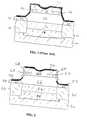
- FIG. 1A typical prior art SiGe heterojunction bipolar transistor is shown, for example, in FIG. 1.
- the SiGe heterojunction bipolar transistor shown in FIG. 1comprises semiconductor substrate 10 of a first conductivity type having sub-collector 14 and collector 16 formed therein. Isolation regions 12 , which are also present in the substrate, define the outer boundaries of the bipolar transistor.
- the bipolar transistor of FIG. 1further includes SiGe layer 20 formed on a surface of substrate 10 as well as isolation regions 12 .
- the SiGe layerincludes polycrystalline Si regions 24 that are formed over the isolation regions and SiGe base region 22 that is formed over the collector and subcollector regions.
- the prior art bipolar transistoralso includes patterned insulator layer 26 formed on the base region and emitter 28 formed on the patterned insulator layer as well as a surface of SiGe base region 22 . Silicide regions 30 are also present in the structure shown in FIG. 1.
- a major problem with the prior art SiGe heterojunction bipolar transistors of the type illustrated in FIG. 1is that the SiGe bipolar yield is significantly reduced because of the presence of shorts which are introduced into the structure during the silicide process. The shorts are caused by the presence of silicide bridges that exist in the structure. As such, a 20-30% yield loss is typically associated with prior art SiGe heterojunction bipolar transistors. The SiGe bipolar yield loss is more pronounced when cobalt disilicide regions are formed in the structure.
- One object of the present inventionis to provide a method of fabricating a SiGe heterojunction bipolar transistor wherein improved SiGe bipolar yield is achieved.
- Another object of the present inventionis to provide a method of fabricating a SiGe heterojunction bipolar transistor wherein the shorts caused during the formation of silicide regions in the structure are substantially eliminated.
- a further object of the present inventionis to provide a method of fabricating a SiGe heterojunction bipolar transistor which prevents bridging between adjacent silicide regions.
- An even further object of the present inventionis to provide a method of fabricating a SiGe heterojunction bipolar transistor using processing steps that are compatible with existing bipolar and CMOS (complementary metal oxide semiconductor) processing steps.
- the passivation layeris formed on the edges of the emitter in the present invention by utilizing a rapid thermal chemical vapor deposition (RTCVD) process which is capable of providing a conformal layer thereon.
- RTCVDrapid thermal chemical vapor deposition
- the passivation layer employed in the present inventionmay be composed of a nitride an oxide, an oxynitride or any combination thereof.
- the method of the present inventioncomprises the steps of:
- the passivation layeris formed from a rapid thermal chemical vapor deposition process which is capable of forming a conformal layer of passivating material on the sidewalls of the emitter.
- the passivating layer employed in the present inventionmay be composed of a nitride, an oxide, an oxynitride or any combination thereof. Of these passivating materials, it is highly preferred in the present invention that the passivation layer be composed of a nitride.
- Another aspect of the present inventionrelates to the SiGe heterojunction bipolar transistor that is fabricated from the above-mentioned processing steps.
- the inventive SiGe heterojunction bipolar transistorcomprises:
- a semiconductor substratehaving a collector and subcollector region formed therein, wherein said collector is formed between isolation regions that are also present in the substrate;
- SiGe layerformed on said substrate, said SiGe layer including polycrystalline Si regions formed above said isolation regions and a SiGe base region formed above said collector and subcollector regions;
- a patterned insulator layerformed on said SiGe base region, said patterned insulator layer having an opening therein; an emitter formed on said patterned insulator layer and in contact with said SiGe base region through said opening, said emitter having exposed sidewalls;
- the passivation layeris employed in the present invention as a means for preventing bridging between adjacent silicide regions which, if present in the structure, causes silicide shorts.
- FIG. 1is a pictorial representation of a prior art SiGe heterojunction bipolar transistor which does not include the passivation layer of the present invention formed on any exposed sidewalls of the emitter.
- FIG. 2is a pictorial representation of the inventive SiGe heterojunction bipolar transistor which includes a conformal passivation layer formed on exposed sidewalls of the emitter.
- FIGS. 3 - 8are pictorial representations of the inventive bipolar transistor through various processing steps of the present invention.
- FIG. 2represents a cross-sectional view of the inventive SiGe heterojunction bipolar transistor.
- the SiGe heterojunction bipolar transistorcomprises semiconductor substrate 50 of a first conductivity type (N or P) having sub-collector region 54 and collector region 56 formed therein.
- Isolation regions 52which are also present in the substrate define the outer boundaries of the bipolar device region and serve to isolate the bipolar device region shown in FIG. 2 from adjacent device regions.
- the SiGe bipolar transistor of FIG. 2also includes SiGe layer 58 formed on substrate 50 as well as isolation regions 52 .
- the SiGe layerincludes polycrystalline Si regions 60 that are formed over isolation regions 52 and SiGe base region 62 which is formed over the collector and subcollector regions.
- the SiGe base regionincludes extrinsic base and intrinsic regions; these regions are not separately labeled in the drawings, but are nevertheless meant to be included within region 62 . It is noted that the extrinsic and intrinsic base regions of the structure are sometimes referred to as the pedestal portion of a bipolar transistor device.
- the bipolar transistor of FIG. 2also comprises a patterned insulator layer 64 which has an opening formed therein and an emitter, i.e., a region of intrinsic polysilicon, 66 formed on said patterned insulator layer and in,contact with the SiGe base region through the opening in the patterned insulator layer.
- the inventive bipolar transistor shown in FIG. 2also includes conformal passivation layer 68 which is present on the exposed sidewalls of emitter 66 ; conformal passivation layer 68 may also be present on sidewalls of the patterned insulator as well as on a portion of the SiGe base region.
- Silicide regions 70are also shown in the inventive bipolar transistor. The silicide regions are formed on the horizontal portion of the emitter as well as exposed portions of SiGe layer 58 .
- the bipolar transistor shown in FIG. 2has improved SiGe bipolar yield because of the presence of the passivation layer which is formed in the structure prior to forming the silicide regions.
- the passivation layerprevents bridging between adjacent silicide regions which typically occurs in prior art SiGe heterojunction bipolar transistors. See FIG. 1
- bipolar yieldmay be improved as much as 20 to 30%; therefore the present invention provides an improved structure compared with prior art SiGe bipolar transistors which do not contain the passivation layer therein.
- FIG. 3shows the bipolar device region of an initial structure that is employed in the present invention.
- the initial structure shown in FIG. 3comprises substrate 50 having sub-collector region 54 , collector region 56 and isolation regions 52 formed therein.
- substrate 50is composed of any semiconducting material including, but not limited to: Si, Ge, SiGe, GaAs, InAs, InP and all other III/V compound semiconductors. Layered substrates comprising the same or different semiconducting material, e.g., Si/Si or Si/SiGe, are also contemplated herein. Of these semiconducting materials, it is preferred that substrate 50 be composed of Si. As mentioned above, the substrate may be a N-type substrate or a P-type substrate depending on the type of device to be subsequently formed.
- the structure of FIG. 3is formed by first forming an oxide layer (not shown) on the surface of substrate 50 using a conventional deposition process such as chemical vapor deposition (CVD), plasma-assisted CVD, or sputtering, or alternatively the oxide layer is grown thermally.
- Sub-collector region 54is then formed in the substrate using a conventional ion implantation step.
- a thick oxidealso not shown, on the order of about 240 nm, is grown on the surface to eliminate implantation damage.
- the thick oxide as well as the previously mentioned oxide layerare removed utilizing an etching process which has a high selectivity for removing oxide as compared to silicon.
- Isolation regions 52are then formed by either using a conventional local oxidation of silicon (LOCOS) process or by utilizing lithography, etching and trench isolation filling. It is noted that the drawings show the formation of isolation trench regions which are formed as follows: A patterned masking layer (not shown) is first formed on the surface of substrate 50 exposing portions of the substrate. Isolation trenches are then etched into the exposed portions of the substrate utilizing a conventional dry etching process such as reactive-ion etching (RIE) or plasma-etching.
- RIEreactive-ion etching
- the trenches thus formedmay be optionally lined with a conventional liner material, i.e., an oxide, and thereafter CVD or another like deposition process is employed to fill the trenches with silicon oxide or another like trench dielectric material.
- a conventional liner materiali.e., an oxide
- CVD or another like deposition processis employed to fill the trenches with silicon oxide or another like trench dielectric material.
- the trench dielectric materialmay optionally be densified after deposition and a conventional planarization process such as chemical-mechanical polishing (CMP) may also be optionally employed.
- CMPchemical-mechanical polishing
- collector region 56is then formed in the bipolar device region (between the two isolation regions shown in FIG. 2) utilizing conventional ion implantation and activation annealing processes that are well known to those skilled in the art.
- the activation annealing processis typically carried out at a temperature of about 950° C. or above for a time of about 30 seconds or less.
- the bipolar device region shown in the drawingsmay be protected by forming a protective material such as Si 3 N 4 thereon, and conventional processing steps which are capable of forming adjacent device regions can be performed. After completion of the adjacent device regions and subsequent protection thereof, the inventive process continues. It should be noted that in some embodiments, the adjacent device regions are formed after completely fabricating the bipolar transistor.
- SiGe layer 58is formed on substrate 50 as well as isolation regions 52 .
- the SiGe layerincludes polycrystalline Si regions 60 that are formed over isolation regions 52 , and SiGe base region 62 which is formed over the collector and subcollector regions.
- the SiGe layeris formed epitaxially utilizing any conventional deposition technique including, but not limited to: ultra-high vacuum chemical vapor deposition (UHVCVD; molecular beam epitaxy (MBE), rapid thermal chemical vapor deposition (RTCVD) and plasma-enhanced chemical vapor deposition (PECVD).
- UHVCVDultra-high vacuum chemical vapor deposition
- MBEmolecular beam epitaxy
- RTCVDrapid thermal chemical vapor deposition
- PECVDplasma-enhanced chemical vapor deposition
- insulator layer 61(which will subsequently become patterned insulator 64 ) is formed on SiGe base layer 62 utilizing a conventional deposition process such as CVD, plasma-assisted CVD, chemical solution deposition and other like deposition processes.
- the insulatormay be a single layer, as is shown in FIG. 5, or it may contain multi-insulator layers.
- the insulator layeris composed of the same or different insulator material which is selected from the group consisting of SiO 2 , Si oxynitride and other like insulators.
- Emitter window opening 63is then formed in insulator layer 61 so as to expose a portion of the SiGe base region, See FIG. 6.
- the emitter window openingis formed utilizing lithography and etching.
- the etching step usedis selective in removing the insulator material as compared to the SiGe layer.
- an intrinsic polysilicon layer(which will subsequently become emitter 66 ) is formed on the patterned insulator and in the emitter window opening by utilizing either a conventional in-situ doping deposition process or deposition followed by ion implantation.
- the polysilicon and the insulatorare then selectively removed so as to form patterned insulator 64 and emitter 66 on SiGe base region 62 , See FIG. 7.
- lithography and etchingare employed in forming the structure shown in FIG. 7. It is should be noted that a single etching process may be employed in removing portions of the intrinsic polysilicon layer and insulator layer 61 , or separate etching steps may be employed in removing these layers. It is noted that in the structure shown in FIG. 7, emitter 66 has exposed sidewalls 69 .
- conformal passivation layer 68is formed on exposed sidewalls 69 of emitter 68 as well as on the vertical sidewalls of patterned insulator 64 and a portion of SiGe base region 62 .
- the conformal passivation layeris formed utilizing a rapid thermal chemical vapor deposition (RTCVD) process.
- the passivation layermay be composed of an oxide, an oxynitride, a nitride, or any combination thereof. Of these materials, it is preferred in the present invention that a nitride passivation layer be employed.
- the nitride passivation layeris formed by a RTCVD process that is carried out in a nitrogen-containing atmosphere such as NO, N 2 O or N 2 , at a temperature of about 700° C. or higher.
- the passivation layercan then be selectively removed using an anisotropic RIE process. This will leave sidewalls protecting the emitter edges and a complete protecting layer over other regions intentionally left passivated via a lithographic process.
- the structure shown in FIG. 8is subjected to a conventional silicidation process which is capable of forming silicide regions 70 in the structure. Specifically, the silicide regions are formed in portions of SiGe layer 58 that are not protected by the passivation layer.
- This step of the present inventionresults in the formation of the structure shown in FIG. 2; note in FIG. 2, no bridging between adjacent silicide regions, as is the case in FIG. 1, is observed.
Landscapes
- Bipolar Transistors (AREA)
Abstract
Description
- The present invention relates to heterojunction bipolar transistors, and more particularly to a method of fabricating a SiGe heterojunction bipolar transistor in which the SiGe bipolar yield is improved by protecting the edges, i.e., sidewalls, of the bipolar emitter with a passivation layer prior to siliciding the silicon surfaces of the bipolar transistor.[0001]
- Significant growth in both high-frequency wired and wireless markets has introduced new opportunities where compound semiconductors such as SiGe have unique advantages over bulk complementary metal oxide semiconductor (CMOS) technology. With the rapid advancement of epitaxial-layer pseudomorphic SiGe deposition processes, epitaxial-base SiGe heterojunction bipolar transistors have been integrated with mainstream advanced CMOS development for wide market acceptance, providing the advantages of SiGe technology for analog and RF circuitry while maintaining the full utilization of the advanced CMOS technology base for digital logic circuitry.[0002]
- A typical prior art SiGe heterojunction bipolar transistor is shown, for example, in FIG. 1. Specifically, the SiGe heterojunction bipolar transistor shown in FIG. 1 comprises[0003]
semiconductor substrate 10 of a first conductivity type having sub-collector14 and collector16 formed therein.Isolation regions 12, which are also present in the substrate, define the outer boundaries of the bipolar transistor. The bipolar transistor of FIG. 1 further includesSiGe layer 20 formed on a surface ofsubstrate 10 as well asisolation regions 12. The SiGe layer includespolycrystalline Si regions 24 that are formed over the isolation regions andSiGe base region 22 that is formed over the collector and subcollector regions. The prior art bipolar transistor also includes patternedinsulator layer 26 formed on the base region andemitter 28 formed on the patterned insulator layer as well as a surface ofSiGe base region 22.Silicide regions 30 are also present in the structure shown in FIG. 1. - A major problem with the prior art SiGe heterojunction bipolar transistors of the type illustrated in FIG. 1 is that the SiGe bipolar yield is significantly reduced because of the presence of shorts which are introduced into the structure during the silicide process. The shorts are caused by the presence of silicide bridges that exist in the structure. As such, a 20-30% yield loss is typically associated with prior art SiGe heterojunction bipolar transistors. The SiGe bipolar yield loss is more pronounced when cobalt disilicide regions are formed in the structure.[0004]
- In view of the above mentioned problem with prior art heterojunction bipolar transistors, there is still a continued need for developing a new and improved method which is capable of fabricating a heterojunction bipolar transistor in which the SiGe bipolar yield loss due to silicide shorts has been substantially eliminated.[0005]
- One object of the present invention is to provide a method of fabricating a SiGe heterojunction bipolar transistor wherein improved SiGe bipolar yield is achieved.[0006]
- Another object of the present invention is to provide a method of fabricating a SiGe heterojunction bipolar transistor wherein the shorts caused during the formation of silicide regions in the structure are substantially eliminated.[0007]
- A further object of the present invention is to provide a method of fabricating a SiGe heterojunction bipolar transistor which prevents bridging between adjacent silicide regions.[0008]
- An even further object of the present invention is to provide a method of fabricating a SiGe heterojunction bipolar transistor using processing steps that are compatible with existing bipolar and CMOS (complementary metal oxide semiconductor) processing steps.[0009]
- These and other objects and advantages are achieved in the present invention by protecting the edges of the emitter with a passivation layer prior to the formation of silicide regions in the structure. The passivation layer is formed on the edges of the emitter in the present invention by utilizing a rapid thermal chemical vapor deposition (RTCVD) process which is capable of providing a conformal layer thereon. The passivation layer employed in the present invention may be composed of a nitride an oxide, an oxynitride or any combination thereof.[0010]
- Specifically, the method of the present invention comprises the steps of:[0011]
- (a) forming a passivation layer on at least exposed sidewalls of an emitter, said emitter is in contact with an underlying SiGe base region through an emitter opening formed in an insulator layer; and[0012]
- (b) siliciding any exposed silicon surfaces so as to form silicide regions therein.[0013]
- In accordance with the present invention, the passivation layer is formed from a rapid thermal chemical vapor deposition process which is capable of forming a conformal layer of passivating material on the sidewalls of the emitter. The passivating layer employed in the present invention may be composed of a nitride, an oxide, an oxynitride or any combination thereof. Of these passivating materials, it is highly preferred in the present invention that the passivation layer be composed of a nitride.[0014]
- Another aspect of the present invention relates to the SiGe heterojunction bipolar transistor that is fabricated from the above-mentioned processing steps. Specifically, the inventive SiGe heterojunction bipolar transistor comprises:[0015]
- a semiconductor substrate having a collector and subcollector region formed therein, wherein said collector is formed between isolation regions that are also present in the substrate;[0016]
- a SiGe layer formed on said substrate, said SiGe layer including polycrystalline Si regions formed above said isolation regions and a SiGe base region formed above said collector and subcollector regions;[0017]
- a patterned insulator layer formed on said SiGe base region, said patterned insulator layer having an opening therein; an emitter formed on said patterned insulator layer and in contact with said SiGe base region through said opening, said emitter having exposed sidewalls;[0018]
- a conformal passivation layer formed on at least said exposed sidewalls of said emitter; and[0019]
- silicide regions formed on exposed portions of said SiGe layer and said emitter not covered by said conformal passivation layer.[0020]
- It is emphasized that the passivation layer is employed in the present invention as a means for preventing bridging between adjacent silicide regions which, if present in the structure, causes silicide shorts.[0021]
- FIG. 1 is a pictorial representation of a prior art SiGe heterojunction bipolar transistor which does not include the passivation layer of the present invention formed on any exposed sidewalls of the emitter.[0022]
- FIG. 2 is a pictorial representation of the inventive SiGe heterojunction bipolar transistor which includes a conformal passivation layer formed on exposed sidewalls of the emitter.[0023]
- FIGS.[0024]3-8 are pictorial representations of the inventive bipolar transistor through various processing steps of the present invention.
- The present invention which provides a method for improving the SiGe bipolar yield of a SiGe bipolar transistor as well as a SiGe heterojunction bipolar transistor will now be described in more detail by referring to the drawings the accompany the present invention. It is noted that in the accompanying drawings, like and corresponding elements are referred to by like reference numerals. Also, for simplicity, only one bipolar device region is shown in the drawings. Other bipolar device regions as well as digital logic circuitry may be formed adjacent to the bipolar device region depicted in the drawings.[0025]
- Reference is first made to FIG. 2 which represents a cross-sectional view of the inventive SiGe heterojunction bipolar transistor. Specifically, the SiGe heterojunction bipolar transistor comprises[0026]
semiconductor substrate 50 of a first conductivity type (N or P) havingsub-collector region 54 andcollector region 56 formed therein.Isolation regions 52 which are also present in the substrate define the outer boundaries of the bipolar device region and serve to isolate the bipolar device region shown in FIG. 2 from adjacent device regions. - The SiGe bipolar transistor of FIG. 2 also includes[0027]
SiGe layer 58 formed onsubstrate 50 as well asisolation regions 52. In accordance with the present invention, the SiGe layer includespolycrystalline Si regions 60 that are formed overisolation regions 52 and SiGebase region 62 which is formed over the collector and subcollector regions. The SiGe base region includes extrinsic base and intrinsic regions; these regions are not separately labeled in the drawings, but are nevertheless meant to be included withinregion 62. It is noted that the extrinsic and intrinsic base regions of the structure are sometimes referred to as the pedestal portion of a bipolar transistor device. - The bipolar transistor of FIG. 2 also comprises a patterned[0028]
insulator layer 64 which has an opening formed therein and an emitter, i.e., a region of intrinsic polysilicon,66 formed on said patterned insulator layer and in,contact with the SiGe base region through the opening in the patterned insulator layer. The inventive bipolar transistor shown in FIG. 2 also includesconformal passivation layer 68 which is present on the exposed sidewalls ofemitter 66;conformal passivation layer 68 may also be present on sidewalls of the patterned insulator as well as on a portion of the SiGe base region.Silicide regions 70 are also shown in the inventive bipolar transistor. The silicide regions are formed on the horizontal portion of the emitter as well as exposed portions ofSiGe layer 58. - It is noted that the bipolar transistor shown in FIG. 2 has improved SiGe bipolar yield because of the presence of the passivation layer which is formed in the structure prior to forming the silicide regions. The passivation layer prevents bridging between adjacent silicide regions which typically occurs in prior art SiGe heterojunction bipolar transistors. See FIG. 1 In the present invention, bipolar yield may be improved as much as 20 to 30%; therefore the present invention provides an improved structure compared with prior art SiGe bipolar transistors which do not contain the passivation layer therein.[0029]
- The method and various materials that are employed in forming the SiGe heterojunction bipolar transistor shown in FIG. 2 will now be described in more detail. Reference is first made to FIG. 3 which shows the bipolar device region of an initial structure that is employed in the present invention. The initial structure shown in FIG. 3 comprises[0030]
substrate 50 havingsub-collector region 54,collector region 56 andisolation regions 52 formed therein. - The structure shown in FIG. 3 is fabricated using conventional processing steps that are well known to those skilled in the art. Moreover, conventional materials are used in fabricating the same. For example,[0031]
substrate 50 is composed of any semiconducting material including, but not limited to: Si, Ge, SiGe, GaAs, InAs, InP and all other III/V compound semiconductors. Layered substrates comprising the same or different semiconducting material, e.g., Si/Si or Si/SiGe, are also contemplated herein. Of these semiconducting materials, it is preferred thatsubstrate 50 be composed of Si. As mentioned above, the substrate may be a N-type substrate or a P-type substrate depending on the type of device to be subsequently formed. - The structure of FIG. 3 is formed by first forming an oxide layer (not shown) on the surface of[0032]
substrate 50 using a conventional deposition process such as chemical vapor deposition (CVD), plasma-assisted CVD, or sputtering, or alternatively the oxide layer is grown thermally.Sub-collector region 54 is then formed in the substrate using a conventional ion implantation step. After the implantation step, a thick oxide (also not shown), on the order of about 240 nm, is grown on the surface to eliminate implantation damage. Next, the thick oxide as well as the previously mentioned oxide layer are removed utilizing an etching process which has a high selectivity for removing oxide as compared to silicon. - [0033]
Isolation regions 52 are then formed by either using a conventional local oxidation of silicon (LOCOS) process or by utilizing lithography, etching and trench isolation filling. It is noted that the drawings show the formation of isolation trench regions which are formed as follows: A patterned masking layer (not shown) is first formed on the surface ofsubstrate 50 exposing portions of the substrate. Isolation trenches are then etched into the exposed portions of the substrate utilizing a conventional dry etching process such as reactive-ion etching (RIE) or plasma-etching. The trenches thus formed may be optionally lined with a conventional liner material, i.e., an oxide, and thereafter CVD or another like deposition process is employed to fill the trenches with silicon oxide or another like trench dielectric material. The trench dielectric material may optionally be densified after deposition and a conventional planarization process such as chemical-mechanical polishing (CMP) may also be optionally employed. - Following the formation of isolation regions in the substrate,[0034]
collector region 56 is then formed in the bipolar device region (between the two isolation regions shown in FIG. 2) utilizing conventional ion implantation and activation annealing processes that are well known to those skilled in the art. The activation annealing process is typically carried out at a temperature of about 950° C. or above for a time of about 30 seconds or less. - At this point of the inventive process, the bipolar device region shown in the drawings may be protected by forming a protective material such as Si[0035]3N4thereon, and conventional processing steps which are capable of forming adjacent device regions can be performed. After completion of the adjacent device regions and subsequent protection thereof, the inventive process continues. It should be noted that in some embodiments, the adjacent device regions are formed after completely fabricating the bipolar transistor.
- The next step of the present invention is shown in FIG. 4. In this figure,[0036]
SiGe layer 58 is formed onsubstrate 50 as well asisolation regions 52. In accordance with the present invention, the SiGe layer includespolycrystalline Si regions 60 that are formed overisolation regions 52, andSiGe base region 62 which is formed over the collector and subcollector regions. - The SiGe layer is formed epitaxially utilizing any conventional deposition technique including, but not limited to: ultra-high vacuum chemical vapor deposition (UHVCVD; molecular beam epitaxy (MBE), rapid thermal chemical vapor deposition (RTCVD) and plasma-enhanced chemical vapor deposition (PECVD). The conditions used in forming the SiGe layer (which are conventional and well known to those skilled in the art) vary depending upon the desired technique employed.[0037]
- Next, and as shown in FIG. 5, insulator layer[0038]61 (which will subsequently become patterned insulator64) is formed on
SiGe base layer 62 utilizing a conventional deposition process such as CVD, plasma-assisted CVD, chemical solution deposition and other like deposition processes. The insulator may be a single layer, as is shown in FIG. 5, or it may contain multi-insulator layers. The insulator layer is composed of the same or different insulator material which is selected from the group consisting of SiO2, Si oxynitride and other like insulators. - [0039]
Emitter window opening 63 is then formed ininsulator layer 61 so as to expose a portion of the SiGe base region, See FIG. 6. The emitter window opening is formed utilizing lithography and etching. The etching step used is selective in removing the insulator material as compared to the SiGe layer. - Following formation of the emitter window opening, an intrinsic polysilicon layer (which will subsequently become emitter[0040]66) is formed on the patterned insulator and in the emitter window opening by utilizing either a conventional in-situ doping deposition process or deposition followed by ion implantation. The polysilicon and the insulator are then selectively removed so as to form patterned
insulator 64 andemitter 66 onSiGe base region 62, See FIG. 7. Specifically, lithography and etching are employed in forming the structure shown in FIG. 7. It is should be noted that a single etching process may be employed in removing portions of the intrinsic polysilicon layer andinsulator layer 61, or separate etching steps may be employed in removing these layers. It is noted that in the structure shown in FIG. 7,emitter 66 has exposedsidewalls 69. - Next, as shown in FIG. 8,[0041]
conformal passivation layer 68 is formed on exposed sidewalls69 ofemitter 68 as well as on the vertical sidewalls of patternedinsulator 64 and a portion ofSiGe base region 62. In accordance with the present invention the conformal passivation layer is formed utilizing a rapid thermal chemical vapor deposition (RTCVD) process. The passivation layer may be composed of an oxide, an oxynitride, a nitride, or any combination thereof. Of these materials, it is preferred in the present invention that a nitride passivation layer be employed. When a nitride passivation layer is to be formed, the nitride passivation layer is formed by a RTCVD process that is carried out in a nitrogen-containing atmosphere such as NO, N2O or N2, at a temperature of about 700° C. or higher. - The passivation layer can then be selectively removed using an anisotropic RIE process. This will leave sidewalls protecting the emitter edges and a complete protecting layer over other regions intentionally left passivated via a lithographic process.[0042]
- Following the passivation of the exposed sidewalls of[0043]
emitter 66, the structure shown in FIG. 8 is subjected to a conventional silicidation process which is capable of formingsilicide regions 70 in the structure. Specifically, the silicide regions are formed in portions ofSiGe layer 58 that are not protected by the passivation layer. This step of the present invention results in the formation of the structure shown in FIG. 2; note in FIG. 2, no bridging between adjacent silicide regions, as is the case in FIG. 1, is observed. - While this invention has been particularly shown and described with respect to preferred embodiments thereof, it will be understood by those skilled in the art that the foregoing and other changes in forms and details may be made without departing from the spirit and scope of the present invention. It is therefore intended that the present invention not be limited to the exact forms and details described and illustrated, but fall within the scope of the appended claims.[0044]
Claims (17)
Priority Applications (1)
| Application Number | Priority Date | Filing Date | Title |
|---|---|---|---|
| US09/773,798US7214593B2 (en) | 2001-02-01 | 2001-02-01 | Passivation for improved bipolar yield |
Applications Claiming Priority (1)
| Application Number | Priority Date | Filing Date | Title |
|---|---|---|---|
| US09/773,798US7214593B2 (en) | 2001-02-01 | 2001-02-01 | Passivation for improved bipolar yield |
Publications (2)
| Publication Number | Publication Date |
|---|---|
| US20020102787A1true US20020102787A1 (en) | 2002-08-01 |
| US7214593B2 US7214593B2 (en) | 2007-05-08 |
Family
ID=25099333
Family Applications (1)
| Application Number | Title | Priority Date | Filing Date |
|---|---|---|---|
| US09/773,798Expired - Fee RelatedUS7214593B2 (en) | 2001-02-01 | 2001-02-01 | Passivation for improved bipolar yield |
Country Status (1)
| Country | Link |
|---|---|
| US (1) | US7214593B2 (en) |
Cited By (2)
| Publication number | Priority date | Publication date | Assignee | Title |
|---|---|---|---|---|
| US20070057374A1 (en)* | 2005-09-13 | 2007-03-15 | International Business Machines Corporation | Embedded barrier for dielectric encapsulation |
| CN102956478A (en)* | 2011-08-24 | 2013-03-06 | 上海华虹Nec电子有限公司 | Compensation method for increase of amplification times of direct current caused by thinning of germanium-silicon edge |
Families Citing this family (1)
| Publication number | Priority date | Publication date | Assignee | Title |
|---|---|---|---|---|
| US8558282B1 (en)* | 2012-09-08 | 2013-10-15 | International Business Machines Corporation | Germanium lateral bipolar junction transistor |
Citations (18)
| Publication number | Priority date | Publication date | Assignee | Title |
|---|---|---|---|---|
| US4691219A (en)* | 1980-07-08 | 1987-09-01 | International Business Machines Corporation | Self-aligned polysilicon base contact structure |
| US4871684A (en)* | 1987-10-29 | 1989-10-03 | International Business Machines Corporation | Self-aligned polysilicon emitter and contact structure for high performance bipolar transistors |
| US4929570A (en)* | 1986-10-06 | 1990-05-29 | National Semiconductor Corporation | Selective epitaxy BiCMOS process |
| US5067002A (en)* | 1987-01-30 | 1991-11-19 | Motorola, Inc. | Integrated circuit structures having polycrystalline electrode contacts |
| US5106767A (en)* | 1990-12-07 | 1992-04-21 | International Business Machines Corporation | Process for fabricating low capacitance bipolar junction transistor |
| US5121184A (en)* | 1991-03-05 | 1992-06-09 | Hewlett-Packard Company | Bipolar transistor containing a self-aligned emitter contact and method for forming transistor |
| US5162255A (en)* | 1989-04-27 | 1992-11-10 | Fujitsu Limited | Method for manufacturing a hetero bipolar transistor |
| US5286661A (en)* | 1992-08-26 | 1994-02-15 | Motorola, Inc. | Method of forming a bipolar transistor having an emitter overhang |
| US5323032A (en)* | 1991-09-05 | 1994-06-21 | Nec Corporation | Dual layer epitaxtial base heterojunction bipolar transistor |
| US5331199A (en)* | 1992-04-30 | 1994-07-19 | International Business Machines Corporation | Bipolar transistor with reduced topography |
| US5336625A (en)* | 1990-11-14 | 1994-08-09 | Samsung Semiconductor Corporation | BiCMOS process with low base recombination current bipolar transistors |
| US5374566A (en)* | 1993-01-27 | 1994-12-20 | National Semiconductor Corporation | Method of fabricating a BiCMOS structure |
| US5504018A (en)* | 1994-06-16 | 1996-04-02 | Nec Corporation | Process of fabricating bipolar transistor having epitaxially grown base layer without deterioration of transistor characteristics |
| US5614758A (en)* | 1991-07-26 | 1997-03-25 | Hewlett-Packard Company | Fully walled emitter-base in a bipolar transistor |
| US5661046A (en)* | 1990-04-02 | 1997-08-26 | National Semiconductor Corporation | Method of fabricating BiCMOS device |
| US5773350A (en)* | 1997-01-28 | 1998-06-30 | National Semiconductor Corporation | Method for forming a self-aligned bipolar junction transistor with silicide extrinsic base contacts and selective epitaxial grown intrinsic base |
| US5897359A (en)* | 1996-12-09 | 1999-04-27 | Electronics And Telecommunications Research Institute | Method of manufacturing a silicon/silicon germanium heterojunction bipolar transistor |
| US5939738A (en)* | 1995-10-25 | 1999-08-17 | Texas Instruments Incorporated | Low base-resistance bipolar transistor |
Family Cites Families (14)
| Publication number | Priority date | Publication date | Assignee | Title |
|---|---|---|---|---|
| EP0147249B1 (en)* | 1983-09-19 | 1989-01-18 | Fairchild Semiconductor Corporation | Method of manufacturing transistor structures having junctions bound by insulating layers, and resulting structures |
| US4987102A (en)* | 1989-12-04 | 1991-01-22 | Motorola, Inc. | Process for forming high purity thin films |
| US5177567A (en)* | 1991-07-19 | 1993-01-05 | Energy Conversion Devices, Inc. | Thin-film structure for chalcogenide electrical switching devices and process therefor |
| JP2971246B2 (en)* | 1992-04-15 | 1999-11-02 | 株式会社東芝 | Method for manufacturing hetero bipolar transistor |
| JPH06151829A (en)* | 1992-11-02 | 1994-05-31 | Kawasaki Steel Corp | Method for manufacturing semiconductor device |
| US5620907A (en)* | 1995-04-10 | 1997-04-15 | Lucent Technologies Inc. | Method for making a heterojunction bipolar transistor |
| US5963789A (en)* | 1996-07-08 | 1999-10-05 | Kabushiki Kaisha Toshiba | Method for silicon island formation |
| FR2756104B1 (en) | 1996-11-19 | 1999-01-29 | Sgs Thomson Microelectronics | MANUFACTURE OF BIPOLAR / CMOS INTEGRATED CIRCUITS |
| US6040225A (en) | 1997-08-29 | 2000-03-21 | The Whitaker Corporation | Method of fabricating polysilicon based resistors in Si-Ge heterojunction devices |
| US6331492B2 (en)* | 1997-12-31 | 2001-12-18 | Texas Instruments Incorporated | Nitridation for split gate multiple voltage devices |
| US6268779B1 (en)* | 1999-03-19 | 2001-07-31 | Telefonaktiebolaget Lm Ericsson (Publ) | Integrated oscillators and tuning circuits |
| US6326652B1 (en)* | 1999-06-18 | 2001-12-04 | Micron Technology, Inc., | CMOS imager with a self-aligned buried contact |
| US6169007B1 (en)* | 1999-06-25 | 2001-01-02 | Applied Micro Circuits Corporation | Self-aligned non-selective thin-epi-base silicon germanium (SiGe) heterojunction bipolar transistor BicMOS process using silicon dioxide etchback |
| US6319775B1 (en)* | 1999-10-25 | 2001-11-20 | Advanced Micro Devices, Inc. | Nitridation process for fabricating an ONO floating-gate electrode in a two-bit EEPROM device |
- 2001
- 2001-02-01USUS09/773,798patent/US7214593B2/ennot_activeExpired - Fee Related
Patent Citations (18)
| Publication number | Priority date | Publication date | Assignee | Title |
|---|---|---|---|---|
| US4691219A (en)* | 1980-07-08 | 1987-09-01 | International Business Machines Corporation | Self-aligned polysilicon base contact structure |
| US4929570A (en)* | 1986-10-06 | 1990-05-29 | National Semiconductor Corporation | Selective epitaxy BiCMOS process |
| US5067002A (en)* | 1987-01-30 | 1991-11-19 | Motorola, Inc. | Integrated circuit structures having polycrystalline electrode contacts |
| US4871684A (en)* | 1987-10-29 | 1989-10-03 | International Business Machines Corporation | Self-aligned polysilicon emitter and contact structure for high performance bipolar transistors |
| US5162255A (en)* | 1989-04-27 | 1992-11-10 | Fujitsu Limited | Method for manufacturing a hetero bipolar transistor |
| US5661046A (en)* | 1990-04-02 | 1997-08-26 | National Semiconductor Corporation | Method of fabricating BiCMOS device |
| US5336625A (en)* | 1990-11-14 | 1994-08-09 | Samsung Semiconductor Corporation | BiCMOS process with low base recombination current bipolar transistors |
| US5106767A (en)* | 1990-12-07 | 1992-04-21 | International Business Machines Corporation | Process for fabricating low capacitance bipolar junction transistor |
| US5121184A (en)* | 1991-03-05 | 1992-06-09 | Hewlett-Packard Company | Bipolar transistor containing a self-aligned emitter contact and method for forming transistor |
| US5614758A (en)* | 1991-07-26 | 1997-03-25 | Hewlett-Packard Company | Fully walled emitter-base in a bipolar transistor |
| US5323032A (en)* | 1991-09-05 | 1994-06-21 | Nec Corporation | Dual layer epitaxtial base heterojunction bipolar transistor |
| US5331199A (en)* | 1992-04-30 | 1994-07-19 | International Business Machines Corporation | Bipolar transistor with reduced topography |
| US5286661A (en)* | 1992-08-26 | 1994-02-15 | Motorola, Inc. | Method of forming a bipolar transistor having an emitter overhang |
| US5374566A (en)* | 1993-01-27 | 1994-12-20 | National Semiconductor Corporation | Method of fabricating a BiCMOS structure |
| US5504018A (en)* | 1994-06-16 | 1996-04-02 | Nec Corporation | Process of fabricating bipolar transistor having epitaxially grown base layer without deterioration of transistor characteristics |
| US5939738A (en)* | 1995-10-25 | 1999-08-17 | Texas Instruments Incorporated | Low base-resistance bipolar transistor |
| US5897359A (en)* | 1996-12-09 | 1999-04-27 | Electronics And Telecommunications Research Institute | Method of manufacturing a silicon/silicon germanium heterojunction bipolar transistor |
| US5773350A (en)* | 1997-01-28 | 1998-06-30 | National Semiconductor Corporation | Method for forming a self-aligned bipolar junction transistor with silicide extrinsic base contacts and selective epitaxial grown intrinsic base |
Cited By (5)
| Publication number | Priority date | Publication date | Assignee | Title |
|---|---|---|---|---|
| US20070057374A1 (en)* | 2005-09-13 | 2007-03-15 | International Business Machines Corporation | Embedded barrier for dielectric encapsulation |
| US7394154B2 (en) | 2005-09-13 | 2008-07-01 | International Business Machines Corporation | Embedded barrier for dielectric encapsulation |
| US20080217777A1 (en)* | 2005-09-13 | 2008-09-11 | International Business Machines Corporation | Embedded barrier for dielectric encapsulation |
| US7968456B2 (en) | 2005-09-13 | 2011-06-28 | International Business Machines Corporation | Method of forming an embedded barrier layer for protection from chemical mechanical polishing process |
| CN102956478A (en)* | 2011-08-24 | 2013-03-06 | 上海华虹Nec电子有限公司 | Compensation method for increase of amplification times of direct current caused by thinning of germanium-silicon edge |
Also Published As
| Publication number | Publication date |
|---|---|
| US7214593B2 (en) | 2007-05-08 |
Similar Documents
| Publication | Publication Date | Title |
|---|---|---|
| US6492238B1 (en) | Bipolar transistor with raised extrinsic base fabricated in an integrated BiCMOS circuit | |
| US6936910B2 (en) | BiCMOS technology on SOI substrates | |
| US7888745B2 (en) | Bipolar transistor with dual shallow trench isolation and low base resistance | |
| CN100411190C (en) | BiCMOS structure and method of forming base in BiCMOS process | |
| US6465870B2 (en) | ESD robust silicon germanium transistor with emitter NP-block mask extrinsic base ballasting resistor with doped facet region | |
| US6656809B2 (en) | Method to fabricate SiGe HBTs with controlled current gain and improved breakdown voltage characteristics | |
| US6846710B2 (en) | Method for manufacturing self-aligned BiCMOS | |
| US6906401B2 (en) | Method to fabricate high-performance NPN transistors in a BiCMOS process | |
| US6674102B2 (en) | Sti pull-down to control SiGe facet growth | |
| US7265018B2 (en) | Method to build self-aligned NPN in advanced BiCMOS technology | |
| US6800921B1 (en) | Method of fabricating a polysilicon capacitor utilizing fet and bipolar base polysilicon layers | |
| JP2004532531A (en) | C implantation to improve the yield of SiGe bipolar | |
| US6777302B1 (en) | Nitride pedestal for raised extrinsic base HBT process | |
| JP4148518B2 (en) | BiCMOS integration with raised external base | |
| US7214593B2 (en) | Passivation for improved bipolar yield | |
| US7132700B1 (en) | SiGe layer having small poly grains | |
| US20030219963A1 (en) | Self-aligned method for fabricating epitaxial base bipolar transistor device |
Legal Events
| Date | Code | Title | Description |
|---|---|---|---|
| AS | Assignment | Owner name:INTERNATIONAL BUSINESS MACHINES CORPORATION, NEW Y Free format text:ASSIGNMENT OF ASSIGNORS INTEREST;ASSIGNORS:COOLBAUGH, DOUGLAS DUANE;GRAY, PETER B.;JOHNSON, DONNA KAYE;AND OTHERS;REEL/FRAME:011547/0328;SIGNING DATES FROM 20010130 TO 20010201 | |
| STCF | Information on status: patent grant | Free format text:PATENTED CASE | |
| FPAY | Fee payment | Year of fee payment:4 | |
| REMI | Maintenance fee reminder mailed | ||
| FPAY | Fee payment | Year of fee payment:8 | |
| SULP | Surcharge for late payment | Year of fee payment:7 | |
| AS | Assignment | Owner name:GLOBALFOUNDRIES U.S. 2 LLC, NEW YORK Free format text:ASSIGNMENT OF ASSIGNORS INTEREST;ASSIGNOR:INTERNATIONAL BUSINESS MACHINES CORPORATION;REEL/FRAME:036550/0001 Effective date:20150629 | |
| AS | Assignment | Owner name:GLOBALFOUNDRIES INC., CAYMAN ISLANDS Free format text:ASSIGNMENT OF ASSIGNORS INTEREST;ASSIGNORS:GLOBALFOUNDRIES U.S. 2 LLC;GLOBALFOUNDRIES U.S. INC.;REEL/FRAME:036779/0001 Effective date:20150910 | |
| AS | Assignment | Owner name:WILMINGTON TRUST, NATIONAL ASSOCIATION, DELAWARE Free format text:SECURITY AGREEMENT;ASSIGNOR:GLOBALFOUNDRIES INC.;REEL/FRAME:049490/0001 Effective date:20181127 | |
| FEPP | Fee payment procedure | Free format text:MAINTENANCE FEE REMINDER MAILED (ORIGINAL EVENT CODE: REM.); ENTITY STATUS OF PATENT OWNER: LARGE ENTITY | |
| LAPS | Lapse for failure to pay maintenance fees | Free format text:PATENT EXPIRED FOR FAILURE TO PAY MAINTENANCE FEES (ORIGINAL EVENT CODE: EXP.); ENTITY STATUS OF PATENT OWNER: LARGE ENTITY | |
| STCH | Information on status: patent discontinuation | Free format text:PATENT EXPIRED DUE TO NONPAYMENT OF MAINTENANCE FEES UNDER 37 CFR 1.362 | |
| FP | Lapsed due to failure to pay maintenance fee | Effective date:20190508 | |
| AS | Assignment | Owner name:GLOBALFOUNDRIES INC., CAYMAN ISLANDS Free format text:RELEASE BY SECURED PARTY;ASSIGNOR:WILMINGTON TRUST, NATIONAL ASSOCIATION;REEL/FRAME:054636/0001 Effective date:20201117 | |
| AS | Assignment | Owner name:GLOBALFOUNDRIES U.S. INC., NEW YORK Free format text:RELEASE BY SECURED PARTY;ASSIGNOR:WILMINGTON TRUST, NATIONAL ASSOCIATION;REEL/FRAME:056987/0001 Effective date:20201117 |