US20020100751A1 - Apparatus and method for atmospheric pressure reactive atom plasma processing for surface modification - Google Patents
Apparatus and method for atmospheric pressure reactive atom plasma processing for surface modificationDownload PDFInfo
- Publication number
- US20020100751A1 US20020100751A1US10/002,483US248301AUS2002100751A1US 20020100751 A1US20020100751 A1US 20020100751A1US 248301 AUS248301 AUS 248301AUS 2002100751 A1US2002100751 A1US 2002100751A1
- Authority
- US
- United States
- Prior art keywords
- plasma
- workpiece
- plasma torch
- torch
- plasma processing
- Prior art date
- Legal status (The legal status is an assumption and is not a legal conclusion. Google has not performed a legal analysis and makes no representation as to the accuracy of the status listed.)
- Granted
Links
- 238000000034methodMethods0.000titleclaimsabstractdescription95
- 238000012545processingMethods0.000titleclaimsabstractdescription46
- 238000012986modificationMethods0.000titledescription3
- 230000004048modificationEffects0.000titledescription3
- 239000000463materialSubstances0.000claimsabstractdescription62
- 239000007789gasSubstances0.000claimsdescription62
- 230000008569processEffects0.000claimsdescription33
- 238000007493shaping processMethods0.000claimsdescription23
- 238000005498polishingMethods0.000claimsdescription18
- 239000002243precursorSubstances0.000claimsdescription16
- 235000012431wafersNutrition0.000claimsdescription15
- 238000005530etchingMethods0.000claimsdescription8
- 238000006243chemical reactionMethods0.000claimsdescription6
- 238000004140cleaningMethods0.000claimsdescription4
- 230000008878couplingEffects0.000claimsdescription3
- 238000010168coupling processMethods0.000claimsdescription3
- 238000005859coupling reactionMethods0.000claimsdescription3
- 239000007788liquidSubstances0.000claimsdescription3
- 239000007787solidSubstances0.000claimsdescription3
- 210000002381plasmaAnatomy0.000description120
- XKRFYHLGVUSROY-UHFFFAOYSA-NArgonChemical compound[Ar]XKRFYHLGVUSROY-UHFFFAOYSA-N0.000description18
- 239000000126substanceSubstances0.000description16
- 125000004429atomChemical group0.000description15
- 238000009616inductively coupled plasmaMethods0.000description14
- 239000012713reactive precursorSubstances0.000description14
- VYPSYNLAJGMNEJ-UHFFFAOYSA-NSilicium dioxideChemical compoundO=[Si]=OVYPSYNLAJGMNEJ-UHFFFAOYSA-N0.000description9
- 229910052786argonInorganic materials0.000description9
- 150000002500ionsChemical class0.000description8
- 239000000203mixtureSubstances0.000description8
- YCKRFDGAMUMZLT-UHFFFAOYSA-NFluorine atomChemical compound[F]YCKRFDGAMUMZLT-UHFFFAOYSA-N0.000description7
- 230000008901benefitEffects0.000description7
- 239000011737fluorineSubstances0.000description7
- 229910052731fluorineInorganic materials0.000description7
- 239000010410layerSubstances0.000description7
- 239000000047productSubstances0.000description7
- 239000000523sampleSubstances0.000description7
- XUIMIQQOPSSXEZ-UHFFFAOYSA-NSiliconChemical compound[Si]XUIMIQQOPSSXEZ-UHFFFAOYSA-N0.000description6
- 238000013459approachMethods0.000description6
- QVGXLLKOCUKJST-UHFFFAOYSA-Natomic oxygenChemical compound[O]QVGXLLKOCUKJST-UHFFFAOYSA-N0.000description6
- 239000011521glassSubstances0.000description6
- 239000001301oxygenSubstances0.000description6
- 229910052760oxygenInorganic materials0.000description6
- 229910052710siliconInorganic materials0.000description6
- 239000010703siliconSubstances0.000description6
- 238000000992sputter etchingMethods0.000description6
- 238000013519translationMethods0.000description6
- 229910004014SiF4Inorganic materials0.000description5
- 238000009826distributionMethods0.000description5
- 230000005284excitationEffects0.000description5
- 238000009499grossingMethods0.000description5
- ABTOQLMXBSRXSM-UHFFFAOYSA-Nsilicon tetrafluorideChemical compoundF[Si](F)(F)FABTOQLMXBSRXSM-UHFFFAOYSA-N0.000description5
- RYGMFSIKBFXOCR-UHFFFAOYSA-NCopperChemical compound[Cu]RYGMFSIKBFXOCR-UHFFFAOYSA-N0.000description4
- 229910052802copperInorganic materials0.000description4
- 239000010949copperSubstances0.000description4
- 230000008021depositionEffects0.000description4
- 230000003628erosive effectEffects0.000description4
- 238000004519manufacturing processMethods0.000description4
- 229910052751metalInorganic materials0.000description4
- 239000002184metalSubstances0.000description4
- 230000003287optical effectEffects0.000description4
- 239000004065semiconductorSubstances0.000description4
- HBMJWWWQQXIZIP-UHFFFAOYSA-Nsilicon carbideChemical compound[Si+]#[C-]HBMJWWWQQXIZIP-UHFFFAOYSA-N0.000description4
- 229910010271silicon carbideInorganic materials0.000description4
- 230000008859changeEffects0.000description3
- 239000007795chemical reaction productSubstances0.000description3
- 238000004891communicationMethods0.000description3
- 238000011109contaminationMethods0.000description3
- 238000010586diagramMethods0.000description3
- 238000010790dilutionMethods0.000description3
- 239000012895dilutionSubstances0.000description3
- 230000000694effectsEffects0.000description3
- 230000003993interactionEffects0.000description3
- 238000003754machiningMethods0.000description3
- 239000000376reactantSubstances0.000description3
- 235000012239silicon dioxideNutrition0.000description3
- OKTJSMMVPCPJKN-UHFFFAOYSA-NCarbonChemical compound[C]OKTJSMMVPCPJKN-UHFFFAOYSA-N0.000description2
- ZAMOUSCENKQFHK-UHFFFAOYSA-NChlorine atomChemical compound[Cl]ZAMOUSCENKQFHK-UHFFFAOYSA-N0.000description2
- GWEVSGVZZGPLCZ-UHFFFAOYSA-NTitan oxideChemical compoundO=[Ti]=OGWEVSGVZZGPLCZ-UHFFFAOYSA-N0.000description2
- MCMNRKCIXSYSNV-UHFFFAOYSA-NZirconium dioxideChemical compoundO=[Zr]=OMCMNRKCIXSYSNV-UHFFFAOYSA-N0.000description2
- 238000005299abrasionMethods0.000description2
- 239000003570airSubstances0.000description2
- 229910052782aluminiumInorganic materials0.000description2
- XAGFODPZIPBFFR-UHFFFAOYSA-NaluminiumChemical compound[Al]XAGFODPZIPBFFR-UHFFFAOYSA-N0.000description2
- 230000015572biosynthetic processEffects0.000description2
- -1but not limited toChemical compound0.000description2
- 229910052799carbonInorganic materials0.000description2
- 239000012707chemical precursorSubstances0.000description2
- 229910052801chlorineInorganic materials0.000description2
- 239000000460chlorineSubstances0.000description2
- 230000003247decreasing effectEffects0.000description2
- 238000013461designMethods0.000description2
- QDOXWKRWXJOMAK-UHFFFAOYSA-Ndichromium trioxideChemical compoundO=[Cr]O[Cr]=OQDOXWKRWXJOMAK-UHFFFAOYSA-N0.000description2
- 230000004907fluxEffects0.000description2
- 239000005350fused silica glassSubstances0.000description2
- 238000000227grindingMethods0.000description2
- 238000010438heat treatmentMethods0.000description2
- XLYOFNOQVPJJNP-ZSJDYOACSA-Nheavy waterSubstances[2H]O[2H]XLYOFNOQVPJJNP-ZSJDYOACSA-N0.000description2
- 230000006698inductionEffects0.000description2
- 150000002739metalsChemical class0.000description2
- 239000010453quartzSubstances0.000description2
- 239000000377silicon dioxideSubstances0.000description2
- 238000006557surface reactionMethods0.000description2
- XOLBLPGZBRYERU-UHFFFAOYSA-Ntin dioxideChemical compoundO=[Sn]=OXOLBLPGZBRYERU-UHFFFAOYSA-N0.000description2
- WKBOTKDWSSQWDR-UHFFFAOYSA-NBromine atomChemical compound[Br]WKBOTKDWSSQWDR-UHFFFAOYSA-N0.000description1
- 229910002480Cu-OInorganic materials0.000description1
- 229910003265NiCr2O4Inorganic materials0.000description1
- 229910020439SiO2+4HFInorganic materials0.000description1
- 239000003082abrasive agentSubstances0.000description1
- 239000012080ambient airSubstances0.000description1
- 238000004458analytical methodMethods0.000description1
- 239000007864aqueous solutionSubstances0.000description1
- 238000000889atomisationMethods0.000description1
- 230000004888barrier functionEffects0.000description1
- 230000005540biological transmissionEffects0.000description1
- GDTBXPJZTBHREO-UHFFFAOYSA-NbromineSubstancesBrBrGDTBXPJZTBHREO-UHFFFAOYSA-N0.000description1
- 229910052794bromiumInorganic materials0.000description1
- 239000006227byproductSubstances0.000description1
- 150000001768cationsChemical class0.000description1
- 238000000576coating methodMethods0.000description1
- 239000010952cobalt-chromeSubstances0.000description1
- 229910052681coesiteInorganic materials0.000description1
- 150000001875compoundsChemical class0.000description1
- 239000000356contaminantSubstances0.000description1
- 238000012937correctionMethods0.000description1
- 229910052906cristobaliteInorganic materials0.000description1
- 238000000354decomposition reactionMethods0.000description1
- 230000007547defectEffects0.000description1
- 230000007812deficiencyEffects0.000description1
- 230000001627detrimental effectEffects0.000description1
- 238000007516diamond turningMethods0.000description1
- 238000003411electrode reactionMethods0.000description1
- 238000005516engineering processMethods0.000description1
- 230000007613environmental effectEffects0.000description1
- 230000005281excited stateEffects0.000description1
- 238000002474experimental methodMethods0.000description1
- 239000010408filmSubstances0.000description1
- 238000001914filtrationMethods0.000description1
- 125000001153fluoro groupChemical groupF*0.000description1
- 230000006870functionEffects0.000description1
- 150000008282halocarbonsChemical class0.000description1
- 238000011065in-situ storageMethods0.000description1
- 238000010884ion-beam techniqueMethods0.000description1
- CPLXHLVBOLITMK-UHFFFAOYSA-Nmagnesium oxideInorganic materials[Mg]=OCPLXHLVBOLITMK-UHFFFAOYSA-N0.000description1
- 150000001247metal acetylidesChemical class0.000description1
- 238000002156mixingMethods0.000description1
- 230000007935neutral effectEffects0.000description1
- GNRSAWUEBMWBQH-UHFFFAOYSA-Nnickel(II) oxideInorganic materials[Ni]=OGNRSAWUEBMWBQH-UHFFFAOYSA-N0.000description1
- 229910052756noble gasInorganic materials0.000description1
- 239000011368organic materialSubstances0.000description1
- 230000037361pathwayEffects0.000description1
- 230000000737periodic effectEffects0.000description1
- 230000000704physical effectEffects0.000description1
- 238000001020plasma etchingMethods0.000description1
- 238000007517polishing processMethods0.000description1
- 239000000843powderSubstances0.000description1
- 230000005855radiationEffects0.000description1
- 229910001404rare earth metal oxideInorganic materials0.000description1
- 230000009257reactivityEffects0.000description1
- 230000006798recombinationEffects0.000description1
- 238000005215recombinationMethods0.000description1
- 238000013341scale-upMethods0.000description1
- 150000003377silicon compoundsChemical class0.000description1
- 229910000679solderInorganic materials0.000description1
- 239000000243solutionSubstances0.000description1
- 238000009987spinningMethods0.000description1
- 239000007921spraySubstances0.000description1
- 230000000087stabilizing effectEffects0.000description1
- 229910052682stishoviteInorganic materials0.000description1
- 238000006467substitution reactionMethods0.000description1
- 239000002344surface layerSubstances0.000description1
- 230000003746surface roughnessEffects0.000description1
- 230000008646thermal stressEffects0.000description1
- 239000010409thin filmSubstances0.000description1
- 229910052905tridymiteInorganic materials0.000description1
- 238000009423ventilationMethods0.000description1
- 238000011179visual inspectionMethods0.000description1
- 230000004580weight lossEffects0.000description1
- 238000003631wet chemical etchingMethods0.000description1
- 238000001039wet etchingMethods0.000description1
Images


Classifications
- H—ELECTRICITY
- H01—ELECTRIC ELEMENTS
- H01L—SEMICONDUCTOR DEVICES NOT COVERED BY CLASS H10
- H01L21/00—Processes or apparatus adapted for the manufacture or treatment of semiconductor or solid state devices or of parts thereof
- H01L21/67—Apparatus specially adapted for handling semiconductor or electric solid state devices during manufacture or treatment thereof; Apparatus specially adapted for handling wafers during manufacture or treatment of semiconductor or electric solid state devices or components ; Apparatus not specifically provided for elsewhere
- H01L21/67005—Apparatus not specifically provided for elsewhere
- H01L21/67011—Apparatus for manufacture or treatment
- H01L21/67092—Apparatus for mechanical treatment
- B—PERFORMING OPERATIONS; TRANSPORTING
- B23—MACHINE TOOLS; METAL-WORKING NOT OTHERWISE PROVIDED FOR
- B23K—SOLDERING OR UNSOLDERING; WELDING; CLADDING OR PLATING BY SOLDERING OR WELDING; CUTTING BY APPLYING HEAT LOCALLY, e.g. FLAME CUTTING; WORKING BY LASER BEAM
- B23K1/00—Soldering, e.g. brazing, or unsoldering
- B23K1/20—Preliminary treatment of work or areas to be soldered, e.g. in respect of a galvanic coating
- B23K1/206—Cleaning
- C—CHEMISTRY; METALLURGY
- C03—GLASS; MINERAL OR SLAG WOOL
- C03C—CHEMICAL COMPOSITION OF GLASSES, GLAZES OR VITREOUS ENAMELS; SURFACE TREATMENT OF GLASS; SURFACE TREATMENT OF FIBRES OR FILAMENTS MADE FROM GLASS, MINERALS OR SLAGS; JOINING GLASS TO GLASS OR OTHER MATERIALS
- C03C15/00—Surface treatment of glass, not in the form of fibres or filaments, by etching
- C—CHEMISTRY; METALLURGY
- C04—CEMENTS; CONCRETE; ARTIFICIAL STONE; CERAMICS; REFRACTORIES
- C04B—LIME, MAGNESIA; SLAG; CEMENTS; COMPOSITIONS THEREOF, e.g. MORTARS, CONCRETE OR LIKE BUILDING MATERIALS; ARTIFICIAL STONE; CERAMICS; REFRACTORIES; TREATMENT OF NATURAL STONE
- C04B41/00—After-treatment of mortars, concrete, artificial stone or ceramics; Treatment of natural stone
- C04B41/53—After-treatment of mortars, concrete, artificial stone or ceramics; Treatment of natural stone involving the removal of at least part of the materials of the treated article, e.g. etching, drying of hardened concrete
- C—CHEMISTRY; METALLURGY
- C04—CEMENTS; CONCRETE; ARTIFICIAL STONE; CERAMICS; REFRACTORIES
- C04B—LIME, MAGNESIA; SLAG; CEMENTS; COMPOSITIONS THEREOF, e.g. MORTARS, CONCRETE OR LIKE BUILDING MATERIALS; ARTIFICIAL STONE; CERAMICS; REFRACTORIES; TREATMENT OF NATURAL STONE
- C04B41/00—After-treatment of mortars, concrete, artificial stone or ceramics; Treatment of natural stone
- C04B41/80—After-treatment of mortars, concrete, artificial stone or ceramics; Treatment of natural stone of only ceramics
- C04B41/91—After-treatment of mortars, concrete, artificial stone or ceramics; Treatment of natural stone of only ceramics involving the removal of part of the materials of the treated articles, e.g. etching
- C—CHEMISTRY; METALLURGY
- C23—COATING METALLIC MATERIAL; COATING MATERIAL WITH METALLIC MATERIAL; CHEMICAL SURFACE TREATMENT; DIFFUSION TREATMENT OF METALLIC MATERIAL; COATING BY VACUUM EVAPORATION, BY SPUTTERING, BY ION IMPLANTATION OR BY CHEMICAL VAPOUR DEPOSITION, IN GENERAL; INHIBITING CORROSION OF METALLIC MATERIAL OR INCRUSTATION IN GENERAL
- C23C—COATING METALLIC MATERIAL; COATING MATERIAL WITH METALLIC MATERIAL; SURFACE TREATMENT OF METALLIC MATERIAL BY DIFFUSION INTO THE SURFACE, BY CHEMICAL CONVERSION OR SUBSTITUTION; COATING BY VACUUM EVAPORATION, BY SPUTTERING, BY ION IMPLANTATION OR BY CHEMICAL VAPOUR DEPOSITION, IN GENERAL
- C23C16/00—Chemical coating by decomposition of gaseous compounds, without leaving reaction products of surface material in the coating, i.e. chemical vapour deposition [CVD] processes
- C23C16/04—Coating on selected surface areas, e.g. using masks
- C23C16/047—Coating on selected surface areas, e.g. using masks using irradiation by energy or particles
- H—ELECTRICITY
- H05—ELECTRIC TECHNIQUES NOT OTHERWISE PROVIDED FOR
- H05H—PLASMA TECHNIQUE; PRODUCTION OF ACCELERATED ELECTRICALLY-CHARGED PARTICLES OR OF NEUTRONS; PRODUCTION OR ACCELERATION OF NEUTRAL MOLECULAR OR ATOMIC BEAMS
- H05H1/00—Generating plasma; Handling plasma
- H05H1/24—Generating plasma
- H05H1/26—Plasma torches
- H05H1/30—Plasma torches using applied electromagnetic fields, e.g. high frequency or microwave energy
- H—ELECTRICITY
- H05—ELECTRIC TECHNIQUES NOT OTHERWISE PROVIDED FOR
- H05H—PLASMA TECHNIQUE; PRODUCTION OF ACCELERATED ELECTRICALLY-CHARGED PARTICLES OR OF NEUTRONS; PRODUCTION OR ACCELERATION OF NEUTRAL MOLECULAR OR ATOMIC BEAMS
- H05H2245/00—Applications of plasma devices
- H05H2245/40—Surface treatments
Definitions
- the field of the inventionrelates to shaping surfaces using a gas plasma.
- optics produced with current or prior art polishing methodscannot withstand the high intensity of light produced by high-powered laser systems.
- One of the engineering challenges in such an advanced systemis the need for a large number of defect-free optics to be produced within an acceptable period of time and at an acceptable cost.
- Subsurface defects in such an opticcan cause cracks to form on the rear surface of lenses exposed to high ultraviolet laser light levels. These cracks can grow until a large fraction of the light is obscured or until the lens fractures. Some of these lenses also serve as a vacuum barrier, making catastrophic failure a serious safety concern.
- Conventional abrasives-based polishingcan be used for many materials. This polishing process is both chemical and mechanical, involving surface and solution chemistry as well as mechanical abrasion. Mechanical abrasion rapidly removes material, but can produce subsurface damage and cause the damage to propagate deeper into the workpiece. The chemical portion dissolves and redeposits glass, forming a relatively smooth surface. The chemical kinetics of redeposition favor the formation of smooth surfaces, as high spots are mechanically abraded away while holes are filled through redeposition.
- This process of redepositioncan lead to problems in some applications. Analysis of the redeposition layer reveals a tremendous number of contaminants, mostly from the abrasive but also from previous polishing steps. This redeposition layer can affect the adhesion and physical properties of optical coatings. Below this redeposition zone can be an underlying zone of damaged glass, up to tens of microns thick or more. When high fluxes of light pass through this zone, damage sites can nucleate and grow, eventually leading to failure of the entire optic. The quality of the polish, and the underlying redeposition layer and subsurface damage, ultimately control how much light can be transmitted through the optics.
- Ion millingis a well-established technique for removing small amounts of material from a surface using a kinetic beam of ions. Some advantages of ion milling include: no surface contact, no weight on the optic, no edge effects, and correction of long spatial wavelength errors.
- RIEreactive ion etch
- PACEPlasma Assisted Chemical Machining
- a major limitation of this capacitively-coupled discharge approachis the requirement that the workpiece be either conductive or less than 10 mm thick.
- etch ratesare dependant on part thickness, decreasing by a factor of ten when thickness changed from 2 to 10 mm. Above 10 mm the rates are too low to be of much use. If metrology is needed in an iterative procedure, the chamber must be vented and pumped down for the next etch step. The convergence rate for PACE is also typically very low, resulting in a long, expensive multi-step process.
- PACE technologywas recently improved by the substitution of a microwave plasma source for the capacitively coupled system, but the rates are still too slow for optics manufacturing.
- a direct current (DC) plasmacan be used at atmospheric pressure to thin wafers.
- DCdirect current
- a direct current (DC) plasmacan be used at atmospheric pressure to thin wafers.
- a plasma Jetand also referred to as Atmospheric Downstream Plasma (ADP)
- ADPAtmospheric Downstream Plasma
- argonas the plasma gas
- the main intent of the deviceis to do backside thinning of processed silicon wafers for smart card and other consumer applications.
- wafersare thinned in a batch mode by placing them on a platten and using planetary type motion to move the sub-aperture plasma in a pseudo-random fashion across the surface.
- atmospheric DC plasma jetssuch as ADP are not well suited for the precise shaping and smoothing of surfaces or for material deposition. Because the reactive gas is mixed with the bulk gas prior to excitation, the reactive species in the plasma are widely distributed across the discharge. This substantially increases the footprint and the minimum feature size that can be etched into a surface. Furthermore, the electrodes that are used to establish the arc are eroded by the reactants. This adds particulates to the gas stream, as well as causing fluctuations in plasma conditions, and accounting for the reduced uniformity compared to RIE systems. Detrimental electrode reactions also preclude the use of oxygen and many other plasma gases.
- CVMChemical Vapor Machining
- RFradio frequency
- ApJetAnother type of plasma jet has been developed to etch and deposit material on surfaces as well as to clean surfaces, known as an “ApJet.”
- This systemconsists of two concentric electrodes that generate a DC plasma which exits through a nozzle. The discharge is at a low temperature, making the process suitable for cleaning temperature-sensitive materials.
- the ApJetis not suitable for precisely shaping and polishing surfaces, as etch rates are low and the electrodes and nozzle erode and deposit material onto the surface. This makes precision control difficult. Furthermore, the ApJet cannot smooth rough surfaces.
- Systems and methods in accordance with the present inventionovercome deficiencies and obstacles in the prior art to produce a highly-controllable, precise, atmospheric, non-contact material removal process. These systems and methods also provide improved processes for shaping geometric surfaces and rapidly shaping hard-to-machine materials, as well as rapidly thinning finished silicon devices with high smoothness and minimal thickness variation.
- One method for shaping a surface of a workpieceinvolves placing the workpiece in a plasma processing chamber that includes a plasma torch, such as an ICP torch.
- a plasma torchsuch as an ICP torch.
- the workpiece and plasma torchare moved with respect to each other, whether by translating and/or rotating the workpiece, the plasma, or both.
- Reactive atom plasma processingis used to shape the surface of the workpiece with the discharge from the plasma torch.
- Reactive atom plasma processingcan also be used for purposes such as to planarize, polish, clean, or thin the workpiece. The processing may cause minimal or no damage to the workpiece underneath the surface, and may involve removing material from the surface of the workpiece.
- Such a system for shaping the surface of a workpiececan involve a plasma torch configured to shape the surface of a workpiece using a reactive plasma process.
- a translatorcan be used to translate the workpiece, the torch, or both, such that the desired shape, planarization, polishing, or cleaning is achieved.
- the torchcan be contained in a plasma processing or other appropriate chamber.
- FIG. 1is a diagram of a system in accordance with one embodiment of the present invention.
- FIG. 2is a diagram of the ICP torch of FIG. 1.
- FIG. 3is a diagram showing relative concentrations of reactive atoms and reactive ions in a plasma discharge that can be used in accordance with one embodiment of the present invention.
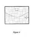
- FIG. 4is a graph of a footprint of a tool that may be used in accordance with one embodiment of the present invention.
- FIG. 5is a flowchart showing a process in accordance with one embodiment of the present invention.
- FIG. 6is a flowchart showing another process in accordance with one embodiment of the present invention.
- FIG. 1shows one embodiment of a reactive atom plasma (RAP) system that can be used in accordance with the present invention.
- FIG. 1shows an ICP torch in a plasma box 106 .
- the torchconsists of an inner tube 134 , an outer tube 138 , and an intermediate tube 136 .
- the inner tube 134has a gas inlet 100 for receiving a reactive precursor gas from the mass flow controller 118 .
- the intermediate tube 136has a gas inlet 102 for receiving an auxiliary gas from the flow controller 118 .
- the outer tube 138has a gas inlet 104 for receiving a plasma gas from the mass flow controller 118 .
- the mass flow controller 118receives the necessary gasses from a number of gas supplies 120 , 122 , 124 , 126 , and controls the amount and rate of gasses passed to the respective tube of the ICP torch.
- the ICP torchgenerates a plasma discharge 108 , which can be used to, for example, shape or polish a workpiece 110 located on a chuck 112 in the workpiece box 114 .
- the plasma box 106 and workpiece box 114are separate, allowing the plasma discharge 108 and/or torch to pass at least partially between the plasma 106 box and the workpiece box 114 .
- the workpiece box 114has an exhaust 132 for carrying away any process gases or products resulting from, for example, the interaction of the plasma discharge 108 and the workpiece 110 . In other embodiments, there may not be separate boxes for the plasma torch and the workpiece.
- the chuck 112 in this embodimentis in communication with a translation stage 116 , which is adapted to translate and/or rotate a workpiece 110 on the chuck 112 with respect to the plasma discharge 108 .
- the translation stage 116is in communication with a computer control system 130 , such as may be programmed to provide the necessary information or control to the translation stage 116 to allow the workpiece 110 to be moved along a proper path to achieve a desired shaping or polishing of the workpiece.
- the computer control system 130is in communication with an RF power supply 128 , which supplies power to the ICP torch.
- the computer control system 130also provides the necessary information to the mass flow controller 118 .
- the torch itselfcan be seen in greater detail in FIG. 2.
- An induction coil 140surrounds the outer tube 138 of the torch near the plasma discharge 144 .
- Current from the RF power supplyflows through the coil 140 around the end of the torch. This energy is coupled into the plasma.
- the excitation zones 142into which the reactive precursor is injected, and the plasma envelop 146 , which can be for example a sheath of argon gas.
- FIG. 5One method for using such a system is shown in FIG. 5.
- a workpieceis placed in a plasma processing chamber that includes a plasma torch 500 .
- At least one of the workpiece and the plasma torchis translated and/or rotated, such as by translating the workpiece with respect to the torch 502 .
- Reactive atom plasma processingis then used to shape the surface of the workpiece with the discharge from the plasma torch 504 .
- the workpieceis again placed in a plasma processing chamber including a plasma torch 600 .
- a controlled flow of precursoris placed in a central channel of the plasma torch 602 .
- a plasma gasis introduced through an outer tube 604 , and an auxiliary gas is introduced through an intermediate tube of the plasma torch 606 .
- the gasescan be introduced relatively simultaneously.
- Energyis coupled to the plasma discharge in an annular region of the plasma torch 608 .
- At least one of the workpiece and the plasma torchis translated and/or rotated, such as by translating the workpiece with respect to the torch 610 .
- Reactive atom plasma processingis then used to shape the surface of the workpiece with the discharge from the plasma torch 612 .
- a reactive atom plasma process in accordance with the present inventionis based, at least in part, on the reactive chemistry of atomic radicals formed by the interaction of a non-reactive precursor chemical with a plasma.
- the atomic radicals formed by the decomposition of a non-reactive precursorinteract with material on the surface of the part being shaped.
- the surface materialis transformed to a gaseous reaction product and leaves the surface.
- a variety of materialscan be processed using different chemical precursors and different plasma compositions.
- the products of the surface reaction in this processmust be a gas under the conditions of the plasma exposure for etching to take place. If not, a surface reaction residue will build up on the surface which will impede further etching.
- the chemistryis specific to fluorine and materials that react with fluorine to form gaseous products. Following are three specific examples where weight loss was measured.
- the materials processedinclude:
- Silicon carbideworks with or without the addition of O 2 .
- the use of O 2can greatly speed the operation.
- One such balanced equationis given by:
- the reactionmay also work with CF 4 supplied by the device and ambient oxygen in the tool enclosure.
- fluorine-containing chemicalsmay be suitable for use as reactive precursors.
- chemicals of the type C n F 2n+2such as C 2 F 6 , C 3 F 8 , and C 4 F10 can be used.
- Fluorine chemicals with other cationsmay also be suitable, as well as F 2 .
- materials that do not contain siliconsuch as, but not limited to, oxides, metals, carbides, and organic materials
- a different reactive atomic speciesmay be appropriate, such as chlorine or bromine.
- Compounds containing these elementsmay also be suitable as reactive precursors.
- An example of such a suitable class of chemicalswould be the class of halocarbons. Mixtures of more than one reactive precursor can also be used.
- the reactive precursor chemicalcan be introduced as a gas.
- a reactive precursorcould also be introduced to the plasma in either liquid or solid form.
- Liquidscan be aspirated into the plasma and fine powders can be nebulized by mixing with a gas before introduction to the plasma.
- an aqueous solution of HFcan be particularly effective because it supplies both fluorine for etching and oxygen for carbon removal, if needed.
- the equations for such a processmay be given by:
- RIErequires a vacuum
- RAP processingcan be used at atmospheric pressure
- RAPhas much higher material removal rates and can be used as a sub-aperture tool to precisely shape surfaces
- RIEis best suited to remove small quantities of material across an entire surface.
- RIEcannot smooth rough surfaces whereas RAP processing rapidly polishes and etches surfaces.
- An inductively-coupled plasmais an excellent source of reactive atoms useful for shaping damage free surfaces.
- An ICP dischargehas previously been used to produce crystalline films of a number of oxides, such as MgO, ZrO 2 , NiO, SnO 2 , TiO 2 , ZnCr 2 O 4 , Cr 2 O 3 , CoCr 2 O 4 , NiCr 2 O 4 , and several rare earth oxides.
- Super conducting thin films of Bi—Pb—Sr—Ca—Cu—Ohave also been fabricated with ICP plasma spray methods.
- the high electrical conductivity of partially ionized gasesmay contribute to the ease of inductively coupled plasma formation at high pressures.
- ICP systemsdo not require electrodes.
- a number of gasescan be used as the host plasma, though argon may be the principle component.
- Atypical dischargecan be characterized by a high current (such as 100 to 1000 amps) and a relatively low voltage (such as 10 to 100 volts).
- the flowing plasmais not in complete thermodynamic equilibrium, but ion and excited state atom populations can be within 10% of equilibrium values.
- Electron densitiescan be high, typically above 10 15 cm ⁇ 3 , which suggests electron temperatures above 15,000K.
- a peak temperature of 10,000Kcan be calculated from the ratio of emission intensities for a set of argon lines (again assuming equilibrium) and gas kinetic temperatures have been estimated to be roughly 6,000K. These high temperatures make the ICP an efficient source for the generation of reactive atoms.
- the current from a 27.12 MHz RF generatorflows through a three turn copper load coil around the top of the torch, such as the one shown in FIG. 2.
- the energyis coupled into the plasma through an annular “skin region” that is located on the outer edge of the plasma nearest the load coil.
- the plasmacan be supported in a quartz tube by the plasma gas, which can be introduced tangentially to form a stabilizing vortex.
- the “skin region”is thinnest along the central axis and the droplets or gas easily penetrate the discharge. As the droplets travel through the plasma they becomes progressively desolvated, atomized, excited, and ionized.
- the relative distribution of ions and atoms in the dischargeis represented in FIG. 3.
- a standard, commercially-available three tube torchcan be used, such as one having three concentric tubes as discussed above.
- the outer tubecan handle the bulk of the plasma gas, while the inner tube can be used to inject the reactive precursor.
- Energycan be coupled into the discharge in an annular region inside the torch. As a result of this coupling zone and the ensuing temperature gradient, a simple way to introduce the reactive gas, or a material to be deposited, is through the center.
- the reactive gascan also be mixed with the plasma gas, although the quartz tube can erode under this configuration.
- Injecting the reactive precursor into the center of the excitation zonehas several important advantages over other techniques.
- Some atmospheric plasma jet systemssuch as ADP, mix the precursor gas in with the plasma gas, creating a uniform plume of reactive species. This exposes the electrodes or plasma tubes to the reactive species, leading to erosion and contamination of the plasma.
- the reactive precursoris introduced around the edge of the excitation zone, which also leads to direct exposure of the electrodes and plasma contamination.
- the reactive species in the RAP systemare enveloped by a sheath of argon, which not only reduces the plasma torch erosion but also reduces interactions between the reactive species and the atmosphere.
- the second of the three tubescan be used to introduce an auxiliary gas, such as at a rate of about 1 L/min.
- the auxiliary gascan have at least two functions. First, the gas can keep the hot plasma away from the inner tube, since even brief contact may seal the inner tube shut. Second, the gas can be used to adjust the position of the discharge in space.
- the inner diameter of the outer tubecan be used to control the size of the discharge. On a standard torch, this can be on the order of about 18 mm. In an attempt to shrink such a system, torches of a two tube design can be constructed, which can have an inner diameter of, for example, about 6 mm, although larger or smaller inner diameters may be appropriate.
- the outer tube gassuch as a plasma gas
- the tangential introductioncan also be maintained with no auxiliary tube.
- a de-mountable systemcan be used, where the tubes are individually held and separately replaced.
- An advantage to such a systemis that the length of the outer tube can be lengthened, allowing the plasma to cool down while preventing reactive radical atoms from reacting with air.
- a small torch erosion problemmay exist due to a minor portion of the precursor not entering the central zone but instead going around the outside of the plasma.
- An increase in skin depthi.e. a thicker energy coupling zone
- a plasma boxcan be used to house the ICP torch.
- the plasma boxcan be used, for example, to shield an operator from radio frequency energy generated during a process, and/or from UV light produced by a plasma.
- the plasma boxcan be kept under a slight negative pressure, such as by hooking it up to a chemical hood exhaust system.
- the entire enclosurecan be constructed, for example, from a single sheet of copper that has been folded, rather than connected from individual plates.
- RFOne of the characteristics of RF is that it travels along a surface of a metal rather than through a metal. RF tends to find and leak out of seams and around door frames. Since it may not be possible to completely avoid edges, the edges of the box can be filled with, for example, silver solder and ground with a radius on them, so that there are no sharp points or edges. Pieces that move, such as doors, can be bolted tight, such as through the use of fasteners.
- Holes and windowscan be formed or cut into the box, such as to allow for air to enter the plasma and sample box, as well as to allow access for servicing, and to provide a place for visual inspection of the system while operating. Since RF cannot escape from holes much smaller than the wavelength of the radiation (for 13.56 MHz the wavelength in vacuum is about 23 meters), a 100 mm square window can have very little leakage.
- the windowscan use welders glass, for example, and the service holes can be covered with copper tape or other UV-filtering material.
- An aluminum sample boxcan be used to contain the workpiece and translation stages. Aluminum plates can be bolted together to form such a box. It may be unnecessary to use copper, as there may be no need to shield from RF.
- the sample boxcan be connected directly to an adjoining torch box, such as through a circular hole. There can also be a window to allow an operator of the system to watch the part during the process, as well as ventilation openings if necessary.
- a main exhaust systemcan be connected to the top of the chamber, although other designs may have the exhaust hose or the stage in a different location, such as may minimize turbulence around the part. There can also be a gauge to measure the pressure differential between the room and the inside of the chamber.
- the main components inside a sample chamber in accordance with the present inventionare the translation stages and the chuck.
- the chuckcan be a relatively simple vacuum system, which can be mounted to the rotary stage and connected to a pump, such as a carbon vane pump, through a rotary or other appropriate connection.
- the chuckcan be smaller than, or equal in size to, the size of the part. If the chuck protrudes past the part, a small amount of chuck material may deposit on the edge or surface.
- Devicessuch as rotometers and mass flow controllers can be used to meter gas flow.
- a systemcan, for example, use mass flow controllers with piezoelectric transducers to monitor gas flow on all lines except the auxiliary.
- a power source and control panelcan be rack mounted. This can be a commercial unit useful for low pressure capacitively coupled discharges.
- the rackcan also contain the stage controller and the electronics for the mass flow controllers.
- the introduction of reactive gas into the plasmacan be controlled by a mass flow controller over a range, for example, of 2000 ml of CF 4 per minute to 0.05 ml per minute, with an accuracy that may be in the range of +/ ⁇ 2.0%.
- a mass flow controllerover a range, for example, of 2000 ml of CF 4 per minute to 0.05 ml per minute, with an accuracy that may be in the range of +/ ⁇ 2.0%.
- the main gas flowsuch as may contain a plasma gas, can serve to supply the discharge with a flowing stream of, for example, argon.
- the flow ratecan be changed over a fairly wide range, such as from zero to about 40 L/min. If the flow is too fast, the plasma may “blow out.” A large flow rate can result in a dilution of both the reactive gas and of the energy put into the system.
- Standard RF unitsoperate at 13.56 MHz, 27.12 MHz, or 40.68 MHz. The frequencies are presently set by the FCC, and may not effect the performance of atomization but may affect the skin depth of the plasma. While a standard RF unit can have a maximum power of 5 to 10 kW, many applications may never require power above 2.5 kW.
- the additional powermay do nothing but deposit more heat on the part.
- Surface heating on the partcan be important to reaction rates and reaction efficiency. Generally, the rates increase with temperature. It may be undesirable to greatly increase the temperature of the part, as reaction products can be produced that condense on cooler areas of the part and on the housing of the device. Too much heat can also cause thermal stress in the part, as well as a change in shape due to thermal expansion.
- the additional energy at the high power settingscan also serve to reduce the number of active species, such as by converting the reactive atoms to ions and reduce their reactivity.
- the processmust produce a volatile reaction product to be successful.
- the plasma temperaturecan be between 5,000 and 15,000° C. As the plasma can be a non-equilibrium system, different techniques for estimating temperature can yield different results. The lower value, 5,000° C., is the gas kinetic temperature and may bear the largest responsibility for heating the part.
- the entire systemcan be mounted on an optical table, or any other appropriate mounting surface or structure. Since the removal tool is a gaseous flow of reactive atoms, it may not be very vibration sensitive. To eliminate any environmental contribution, a clean room or other appropriate enclosure can be built around the sample chamber and torch box.
- One advantage of a system in accordance with the present inventionis the dynamic range of material removal.
- the reactive gascan be delivered in such minute quantities that single atomic layers are removed, such as over a period of seconds or even minutes.
- the processcan remove at least grams of material per minute. While they might not be practical for material removal, very low etch rates can be important for modifying the surface of materials treated with the plasma.
- a dynamic range of five orders of magnitude in etch rateis available in one embodiment, although additional orders of magnitude in etch rate are possible using different ranges and mixtures.
- a high endsuch as may be achieved by confining a precursor to the central channel, it is possible to introduce 1000 ml/min of 100% CF 4 .
- a 1% mix of CF 4 in argoncan be delivered to a central channel with a flow rate of 1 ml/min.
- Etch ratescan be reduced by two more orders of magnitude such as by using a flow controller that operates, for example, from 0 to 10 ml/min and/or by a further 10 ⁇ or other appropriate dilution of the gas.
- FIG. 4is a probe trace of a pit produced by a 1.5 kW plasma with a reactive gas flow rate of 50 mls/minute over a 5 minute period.
- the distance from the load coils (energy induction zone) to the part surfacewas 25 mm.
- the tool shape produced by the plasma systemcan be extremely shallow and broad, which can relax the requirements for precision X-Y positioning of the tool or the part.
- the footprint of the plasma dischargecan be stable and reproducible, and dependant on controllable parameters. Fairly similar etch rates can be produced if similar systems are run under identical conditions, and the same system can be highly reproducible from day to day. For extremely precise surfaces, the footprint of the tool may need to be measured before each removal step. It may also be possible, however, to determine the footprint as a by product of the iterative shaping process.
- any shape on the partis required, other than a Gaussian depression of various depths, it may be necessary to translate and/or rotate the part relative to the torch, although it may also be possible to translate and/or rotate the torch with respect to the part, or both with respect to each other. If the torch is held stationary and lowered into the part a depression or pit may result. If the torch translates across the part while spinning, a trench may be produced. The floor of the trench can take on the characteristics of the distribution of reactive species in the torch, and also can be determined by how closely the torch paths approach each other on subsequent passes. It may be necessary to move two stages at the same time. To accomplish this, a second controller can be used, such as may be computer- or machine-controlled. A basic system can be limited to a constant rotation speed, with the translation speed across the part being controlled in a stepwise fashion (i.e. go a certain distance at a fixed speed and at a certain point change the speed).
- a rough partcan be measured for which a fairly accurate estimate of the footprint is known, such as from previous experiments.
- the final desired part shapemay be known, and a pathway for the tool can be calculated to get the final shape from all of the input variables, including such input variables as initial part shape, plasma conditions, dwell time, and removal behavior of the workpiece material.
- the part shapecould be accurately measured and compared with the desired shape. The difference may be the error in the assumption of the footprint shape.
- the partcan be rotated as it is translated in front of the discharge.
- the speed of the torch across the surfacemay need to be constant.
- One of the more surprising and interesting features of systems in accordance with the present inventionis the planarization and/or polishing of rough surfaces.
- Parameters which can dictate the time required to polish glass or other suitable materials with the plasma systeminclude the concentration of species in the plasma gas (both reactants and products) and the temperature of the surface and surrounding gas. Exchange of species on and off the surface, as well as the local redeposition of material during etching, can be principally responsible for the rapid smoothing of rough surfaces, resulting in planarization on at least a local scale.
- the relatively high concentration of species in the plasma, and the local equilibrium established across the boundary layer by this process,can explain why other lower pressure plasma systems such as PACE do not exhibit such a smoothing effect.
- the higher pressure gascan reduce the mean free path of the products, keeping the products in the surface region for a greater amount of time.
- the higher pressure gascan have a greater heat capacity, keeping the near surface region of the solid at a higher temperature. While low pressure plasma temperatures may be the same, the actual amount of heat deposited on the surface using an atmospheric pressure plasma system can be greater due to the higher flux of gas. This is evident in the fact that one system in accordance with the present invention uses a 1.5 to 2.25 kW plasma while the PACE and microwave devices commonly run at a few hundred watts in a maximum configuration.
- Another way to change the amount of material available for deposition, and to affect the rate of planarization or smoothing,is to add a reactant into the plasma that would cause deposition while the fluorine atoms cause etching .
- a combination of some volatile silicon compound with the addition of oxygenmay be sufficient.
- An equilibrium-deposition state in accordance with the present inventionis not the same as previous plasma deposition, as the process does not simply fill in holes but rather involves a local redistribution of material at the surface. This may be important for applications where it is necessary that the structure of the final surface material be nearly identical to the bulk phase.
Landscapes
- Chemical & Material Sciences (AREA)
- Engineering & Computer Science (AREA)
- Materials Engineering (AREA)
- Physics & Mathematics (AREA)
- Ceramic Engineering (AREA)
- Organic Chemistry (AREA)
- Mechanical Engineering (AREA)
- Structural Engineering (AREA)
- Plasma & Fusion (AREA)
- Chemical Kinetics & Catalysis (AREA)
- General Chemical & Material Sciences (AREA)
- Microelectronics & Electronic Packaging (AREA)
- Power Engineering (AREA)
- Geochemistry & Mineralogy (AREA)
- Toxicology (AREA)
- Condensed Matter Physics & Semiconductors (AREA)
- General Physics & Mathematics (AREA)
- Manufacturing & Machinery (AREA)
- Computer Hardware Design (AREA)
- Health & Medical Sciences (AREA)
- Life Sciences & Earth Sciences (AREA)
- Electromagnetism (AREA)
- Metallurgy (AREA)
- Spectroscopy & Molecular Physics (AREA)
- Drying Of Semiconductors (AREA)
- ing And Chemical Polishing (AREA)
- Treatments Of Macromolecular Shaped Articles (AREA)
- Plasma Technology (AREA)
- Physical Or Chemical Processes And Apparatus (AREA)
- Cleaning Or Drying Semiconductors (AREA)
- Cleaning In General (AREA)
Abstract
Description
- This application claims priority to U.S. Provisional patent application No. 60/265,332, filed Jan. 30, 2001, entitled APPARATUS AND METHOD FOR ATMOSPHERIC PRESSURE REACTIVE ATOM PLASMA PROCESSING FOR SHAPING OF DAMAGE FREE SURFACES.[0001]
- This application is cross-referenced and incorporated herein by reference.[0002]
- [0003] The U.S. Government has rights in this invention pursuant to Contract No. W-7405-ENG-48 between the United States Department of Energy and the University of California.
- The following application is cross-referenced and incorporated herein by reference:[0004]
- U.S. Patent Application No. _________entitled APPARATUS AND METHOD FOR ATMOSPHERIC PRESSURE REACTIVE ATOM PLASMA PROCESSING FOR SHAPING OF DAMAGE FREE SURFACES, inventor Jeffrey W. Carr, filed Nov. 1, 2001.[0005]
- The field of the invention relates to shaping surfaces using a gas plasma.[0006]
- Modern materials present a number of formidable challenges to the fabricators of a wide range of optical, semiconductor, and electronic components, many of which require precision shaping, smoothing, and polishing. Current methods, such as conventional grinding and polishing, have a number of disadvantages. Physical contact methods, such as grinding, abrasive polishing, diamond turning and ion milling, involve physical force at the microscopic scale and can create damage in the subsurface of the material being treated. Physical contact methods also have a trade-off between speed and quality. Smooth surfaces can require the use of very slow material removal rates, while hard materials such as silicon carbide can be extremely difficult to polish. Soft or delicate structures can also be difficult to polish, as the physical force involved can crack or bend the structures. Some materials such as glass can also end up with a surface layer of redeposited material, which can affect the properties and behavior of the manufactured component.[0007]
- Damage-free Laser Optics[0008]
- In one example of such a manufacturing challenge, optics produced with current or prior art polishing methods cannot withstand the high intensity of light produced by high-powered laser systems. One of the engineering challenges in such an advanced system is the need for a large number of defect-free optics to be produced within an acceptable period of time and at an acceptable cost. Subsurface defects in such an optic can cause cracks to form on the rear surface of lenses exposed to high ultraviolet laser light levels. These cracks can grow until a large fraction of the light is obscured or until the lens fractures. Some of these lenses also serve as a vacuum barrier, making catastrophic failure a serious safety concern.[0009]
- Conventional abrasives-based polishing can be used for many materials. This polishing process is both chemical and mechanical, involving surface and solution chemistry as well as mechanical abrasion. Mechanical abrasion rapidly removes material, but can produce subsurface damage and cause the damage to propagate deeper into the workpiece. The chemical portion dissolves and redeposits glass, forming a relatively smooth surface. The chemical kinetics of redeposition favor the formation of smooth surfaces, as high spots are mechanically abraded away while holes are filled through redeposition.[0010]
- This process of redeposition can lead to problems in some applications. Analysis of the redeposition layer reveals a tremendous number of contaminants, mostly from the abrasive but also from previous polishing steps. This redeposition layer can affect the adhesion and physical properties of optical coatings. Below this redeposition zone can be an underlying zone of damaged glass, up to tens of microns thick or more. When high fluxes of light pass through this zone, damage sites can nucleate and grow, eventually leading to failure of the entire optic. The quality of the polish, and the underlying redeposition layer and subsurface damage, ultimately control how much light can be transmitted through the optics.[0011]
- In order to produce optics capable of routinely withstanding laser intensities as high as 12 J/cm[0012]2,a process is required to remove the 20-30 microns of damaged material. Conventional polishing can be used to remove this damage layer, but it must be done very slowly—on the order of about 0.1 μm per hour. Polishing for this length of time also necessitates periodic checks of the shape of the part using precision metrology.
- Wet Etching[0013]
- Another approach to removing the damage layer in an optic is a wet chemical etch. In such a process, only a limited amount of material can be removed before the surface becomes excessively pitted, with a resulting increase in the amount of light scattered by the optic. Optics processed by wet etch have been tested, with the disappointing result that the damage threshold was unaffected.[0014]
- Ion milling[0015]
- Another approach utilizes ion milling after conventional polishing. Ion milling is a well-established technique for removing small amounts of material from a surface using a kinetic beam of ions. Some advantages of ion milling include: no surface contact, no weight on the optic, no edge effects, and correction of long spatial wavelength errors.[0016]
- There are numerous disadvantages to ion milling, however, including high surface temperatures, an increase in surface roughness, and the need for vacuum. The temperature is dependant on beam current, so that an increase in etch rate produces an increase in temperature often surpasses several hundred ° C. Nearly all heat must be removed through the chuck, usually requiring a good thermal connection between the workpiece and the holder. This is difficult when working on transmission optics because they must be held by the edges so as not to damage the polished surface. Further, ion beams cannot smooth surfaces. For small amounts of material removal, roughness can be held constant. Large amounts of material removal cause an unfortunate increase in roughness.[0017]
- Reduced Pressure Plasma Methods[0018]
- Another approach involves plasma etching at reduced temperature, which is used extensively in the semiconductor industry for processing of a wide variety of materials including semiconductors, metals and glasses. Reactive ions are believed to be responsible for the majority of material removal, leading the technique to be known as reactive ion etch (RIE). Considerable effort has been put into developing plasmas with uniform etch rates over the entire discharge, making RIE unsuitable for the production of figured precision components. The greatest practical drawback to RIE for precision finishing of optical components is the need for vacuum and a low material removal rate. Translating either the source or workpiece with precision on a complicated path inside a vacuum chamber is challenging, especially in the case of large optics. In-situ metrology would also be awkward.[0019]
- A modified RIE for polishing at reduced pressure has been built using a capacitively coupled discharge. Named “Plasma Assisted Chemical Machining” (PACE), the system has been successful in shaping and polishing fused silica. While the parts polished by PACE have shown no evidence of subsurface damage or surface contamination, it has been found that greater sub-surface damage present before etching resulted in an increased roughness after etching.[0020]
- A major limitation of this capacitively-coupled discharge approach is the requirement that the workpiece be either conductive or less than 10 mm thick. In addition, etch rates are dependant on part thickness, decreasing by a factor of ten when thickness changed from 2 to 10 mm. Above 10 mm the rates are too low to be of much use. If metrology is needed in an iterative procedure, the chamber must be vented and pumped down for the next etch step. The convergence rate for PACE is also typically very low, resulting in a long, expensive multi-step process. PACE technology was recently improved by the substitution of a microwave plasma source for the capacitively coupled system, but the rates are still too slow for optics manufacturing.[0021]
- Atmospheric Pressure Plasma Methods[0022]
- In yet another approach, a direct current (DC) plasma can be used at atmospheric pressure to thin wafers. Originally called a “Plasma Jet” and also referred to as Atmospheric Downstream Plasma (ADP), such a system uses argon as the plasma gas, with a trace amount of fluorine or chlorine for reactive atom production. The main intent of the device is to do backside thinning of processed silicon wafers for smart card and other consumer applications. With the ADP tool, wafers are thinned in a batch mode by placing them on a platten and using planetary type motion to move the sub-aperture plasma in a pseudo-random fashion across the surface.[0023]
- Unfortunately, atmospheric DC plasma jets such as ADP are not well suited for the precise shaping and smoothing of surfaces or for material deposition. Because the reactive gas is mixed with the bulk gas prior to excitation, the reactive species in the plasma are widely distributed across the discharge. This substantially increases the footprint and the minimum feature size that can be etched into a surface. Furthermore, the electrodes that are used to establish the arc are eroded by the reactants. This adds particulates to the gas stream, as well as causing fluctuations in plasma conditions, and accounting for the reduced uniformity compared to RIE systems. Detrimental electrode reactions also preclude the use of oxygen and many other plasma gases.[0024]
- Another plasma process, known as Chemical Vapor Machining (CVM), is a radio frequency (RF) plasma process that has been used to slice silicon. This plasma is generated around a wire or blade electrode immersed in a noble gas atmosphere containing a trace of reactive components. Like the PACE process it closely resembles, material removal through CVM is entirely chemical in nature. The damage for CVM and wet chemical etching are similar, close to the intrinsic damage typically found in silicon used in the semiconductor industry.[0025]
- Several performance characteristics limit the applications of CVM. First, the non-rotationally symmetric nature of the footprint makes the process difficult to model and control. Process rates are limited by the rate at which the plasma converts the reactive precursor gas into radical atoms. The device is difficult to scale up, limiting the maximum removal rate and the practical limit for fine-scale material removal. While no vacuum is required for CVM, the workpiece must be enclosed in a vessel to contain the plasma atmosphere.[0026]
- Another type of plasma jet has been developed to etch and deposit material on surfaces as well as to clean surfaces, known as an “ApJet.” This system consists of two concentric electrodes that generate a DC plasma which exits through a nozzle. The discharge is at a low temperature, making the process suitable for cleaning temperature-sensitive materials. The ApJet is not suitable for precisely shaping and polishing surfaces, as etch rates are low and the electrodes and nozzle erode and deposit material onto the surface. This makes precision control difficult. Furthermore, the ApJet cannot smooth rough surfaces.[0027]
- Systems and methods in accordance with the present invention overcome deficiencies and obstacles in the prior art to produce a highly-controllable, precise, atmospheric, non-contact material removal process. These systems and methods also provide improved processes for shaping geometric surfaces and rapidly shaping hard-to-machine materials, as well as rapidly thinning finished silicon devices with high smoothness and minimal thickness variation.[0028]
- One method for shaping a surface of a workpiece involves placing the workpiece in a plasma processing chamber that includes a plasma torch, such as an ICP torch. The workpiece and plasma torch are moved with respect to each other, whether by translating and/or rotating the workpiece, the plasma, or both. Reactive atom plasma processing is used to shape the surface of the workpiece with the discharge from the plasma torch. Reactive atom plasma processing can also be used for purposes such as to planarize, polish, clean, or thin the workpiece. The processing may cause minimal or no damage to the workpiece underneath the surface, and may involve removing material from the surface of the workpiece.[0029]
- Also included in the present invention are tools and systems for accomplishing these and other methods. Such a system for shaping the surface of a workpiece can involve a plasma torch configured to shape the surface of a workpiece using a reactive plasma process. A translator can be used to translate the workpiece, the torch, or both, such that the desired shape, planarization, polishing, or cleaning is achieved. The torch can be contained in a plasma processing or other appropriate chamber.[0030]
- FIG. 1 is a diagram of a system in accordance with one embodiment of the present invention.[0031]
- FIG. 2 is a diagram of the ICP torch of FIG. 1.[0032]
- FIG. 3 is a diagram showing relative concentrations of reactive atoms and reactive ions in a plasma discharge that can be used in accordance with one embodiment of the present invention.[0033]
- FIG. 4 is a graph of a footprint of a tool that may be used in accordance with one embodiment of the present invention.[0034]
- FIG. 5 is a flowchart showing a process in accordance with one embodiment of the present invention.[0035]
- FIG. 6 is a flowchart showing another process in accordance with one embodiment of the present invention.[0036]
- Systems and methods in accordance with the present invention have advantages over prior art systems, such as PACE and chemical vapor machining, in that the number of potential products increases to include devices fabricated from heat sensitive components and heterogeneous materials that are typically difficult to polish by chemical means. Polishing and planarization are now be possible with little heat gain and minimal material removal.[0037]
- FIG. 1 shows one embodiment of a reactive atom plasma (RAP) system that can be used in accordance with the present invention. FIG. 1 shows an ICP torch in a[0038]
plasma box 106. The torch consists of aninner tube 134, anouter tube 138, and anintermediate tube 136. Theinner tube 134 has agas inlet 100 for receiving a reactive precursor gas from themass flow controller 118. Theintermediate tube 136 has agas inlet 102 for receiving an auxiliary gas from theflow controller 118. Theouter tube 138 has agas inlet 104 for receiving a plasma gas from themass flow controller 118. Themass flow controller 118 receives the necessary gasses from a number ofgas supplies plasma discharge 108, which can be used to, for example, shape or polish aworkpiece 110 located on achuck 112 in theworkpiece box 114. In this embodiment, theplasma box 106 andworkpiece box 114 are separate, allowing theplasma discharge 108 and/or torch to pass at least partially between theplasma 106 box and theworkpiece box 114. Theworkpiece box 114 has anexhaust 132 for carrying away any process gases or products resulting from, for example, the interaction of theplasma discharge 108 and theworkpiece 110. In other embodiments, there may not be separate boxes for the plasma torch and the workpiece. - The[0039]
chuck 112 in this embodiment is in communication with atranslation stage 116, which is adapted to translate and/or rotate aworkpiece 110 on thechuck 112 with respect to theplasma discharge 108. Thetranslation stage 116 is in communication with acomputer control system 130, such as may be programmed to provide the necessary information or control to thetranslation stage 116 to allow theworkpiece 110 to be moved along a proper path to achieve a desired shaping or polishing of the workpiece. Thecomputer control system 130 is in communication with anRF power supply 128, which supplies power to the ICP torch. Thecomputer control system 130 also provides the necessary information to themass flow controller 118. - The torch itself can be seen in greater detail in FIG. 2. An[0040]
induction coil 140 surrounds theouter tube 138 of the torch near theplasma discharge 144. Current from the RF power supply flows through thecoil 140 around the end of the torch. This energy is coupled into the plasma. Also shown are theexcitation zones 142, into which the reactive precursor is injected, and theplasma envelop 146, which can be for example a sheath of argon gas. - One method for using such a system is shown in FIG. 5. In this method, a workpiece is placed in a plasma processing chamber that includes a[0041]
plasma torch 500. At least one of the workpiece and the plasma torch is translated and/or rotated, such as by translating the workpiece with respect to thetorch 502. Reactive atom plasma processing is then used to shape the surface of the workpiece with the discharge from theplasma torch 504. - In another method, shown in FIG. 6, the workpiece is again placed in a plasma processing chamber including a[0042]
plasma torch 600. A controlled flow of precursor is placed in a central channel of theplasma torch 602. A plasma gas is introduced through anouter tube 604, and an auxiliary gas is introduced through an intermediate tube of theplasma torch 606. The gases can be introduced relatively simultaneously. Energy is coupled to the plasma discharge in an annular region of theplasma torch 608. At least one of the workpiece and the plasma torch is translated and/or rotated, such as by translating the workpiece with respect to thetorch 610. Reactive atom plasma processing is then used to shape the surface of the workpiece with the discharge from theplasma torch 612. - Chemistry[0043]
- A reactive atom plasma process in accordance with the present invention is based, at least in part, on the reactive chemistry of atomic radicals formed by the interaction of a non-reactive precursor chemical with a plasma. In one such process, the atomic radicals formed by the decomposition of a non-reactive precursor interact with material on the surface of the part being shaped. The surface material is transformed to a gaseous reaction product and leaves the surface. A variety of materials can be processed using different chemical precursors and different plasma compositions. The products of the surface reaction in this process must be a gas under the conditions of the plasma exposure for etching to take place. If not, a surface reaction residue will build up on the surface which will impede further etching.[0044]
- In one process in accordance with the present invention, the chemistry is specific to fluorine and materials that react with fluorine to form gaseous products. Following are three specific examples where weight loss was measured. The materials processed include:[0045]
- Silicon dioxide (fused quartz) where the balanced reaction of concern is[0046]
- SiO2+CF4→SiF4+CO2
- Silicon carbide works with or without the addition of O[0047]2. The use of O2can greatly speed the operation. One such balanced equation is given by:
- SiC+CF4+2O2O→SiF4+2CO2
- Silicon works with or without addition of oxygen to the plasma. Oxygen can also be supplied by the ambient air. A balanced equation that can be used with the process is given by:[0048]
- Si+CF4+O2→SiF4+CO2
- The reaction may also work with CF[0049]4supplied by the device and ambient oxygen in the tool enclosure.
- Other fluorocarbons and molecules containing fluorine can work as well. SF[0050]6has been used as the chemical precursor to successfully etch silica glass. The equation can be the same as for CF4, such as may be given by:
- 3SiO2+2SF6→3SiF4+2SO2+O2
- or[0051]
- 3SiO2+2SF6→3SiF4+2SO3
- In addition to SF[0052]6, a large number of fluorine-containing chemicals may be suitable for use as reactive precursors. For example, chemicals of the type CnF2n+2such as C2F6, C3F8, and C4F10 can be used. Fluorine chemicals with other cations may also be suitable, as well as F2. For work on materials that do not contain silicon, such as, but not limited to, oxides, metals, carbides, and organic materials, a different reactive atomic species may be appropriate, such as chlorine or bromine. Compounds containing these elements may also be suitable as reactive precursors. An example of such a suitable class of chemicals would be the class of halocarbons. Mixtures of more than one reactive precursor can also be used.
- In the above examples, the reactive precursor chemical can be introduced as a gas. Such a reactive precursor could also be introduced to the plasma in either liquid or solid form. Liquids can be aspirated into the plasma and fine powders can be nebulized by mixing with a gas before introduction to the plasma. In fact, an aqueous solution of HF can be particularly effective because it supplies both fluorine for etching and oxygen for carbon removal, if needed. The equations for such a process may be given by:[0053]
- SiO2+4HF→SiF4+2H2O
- or[0054]
- SiC+4HF+2O2→SiF4+CO2+2H2O
- Such a process has several advantages over the RIE process. RIE requires a vacuum, whereas RAP processing can be used at atmospheric pressure. RAP has much higher material removal rates and can be used as a sub-aperture tool to precisely shape surfaces, whereas RIE is best suited to remove small quantities of material across an entire surface. Finally, RIE cannot smooth rough surfaces whereas RAP processing rapidly polishes and etches surfaces.[0055]
- ICP Plasma Torch[0056]
- An inductively-coupled plasma (ICP) is an excellent source of reactive atoms useful for shaping damage free surfaces. An ICP discharge has previously been used to produce crystalline films of a number of oxides, such as MgO, ZrO[0057]2, NiO, SnO2, TiO2, ZnCr2O4, Cr2O3, CoCr2O4, NiCr2O4, and several rare earth oxides. Super conducting thin films of Bi—Pb—Sr—Ca—Cu—O have also been fabricated with ICP plasma spray methods.
- The high electrical conductivity of partially ionized gases (for example 120 ohm/cm-1 at 15,000° K. for argon) may contribute to the ease of inductively coupled plasma formation at high pressures. ICP systems do not require electrodes. A number of gases can be used as the host plasma, though argon may be the principle component. Atypical discharge can be characterized by a high current (such as 100 to 1000 amps) and a relatively low voltage (such as 10 to 100 volts). The flowing plasma is not in complete thermodynamic equilibrium, but ion and excited state atom populations can be within 10% of equilibrium values. Electron densities can be high, typically above 10[0058]15cm−3, which suggests electron temperatures above 15,000K. A peak temperature of 10,000K can be calculated from the ratio of emission intensities for a set of argon lines (again assuming equilibrium) and gas kinetic temperatures have been estimated to be roughly 6,000K. These high temperatures make the ICP an efficient source for the generation of reactive atoms.
- The current from a 27.12 MHz RF generator flows through a three turn copper load coil around the top of the torch, such as the one shown in FIG. 2. The energy is coupled into the plasma through an annular “skin region” that is located on the outer edge of the plasma nearest the load coil. The plasma can be supported in a quartz tube by the plasma gas, which can be introduced tangentially to form a stabilizing vortex. The “skin region” is thinnest along the central axis and the droplets or gas easily penetrate the discharge. As the droplets travel through the plasma they becomes progressively desolvated, atomized, excited, and ionized. The relative distribution of ions and atoms in the discharge is represented in FIG. 3. Spatial profiles at five places in the plasma indicate that the excited ion population decays faster than that of the neutral atoms, most likely a result of ion-electron recombination. The maximum atomic emission from the material injected into the plasma occurs several millimeters above the load coil near the visible tip of the discharge ([0059]
zone 3 and4). Radiative decay in this region is used to spectroscopically determine the composition of the injected material. - A standard, commercially-available three tube torch can be used, such as one having three concentric tubes as discussed above. The outer tube can handle the bulk of the plasma gas, while the inner tube can be used to inject the reactive precursor. Energy can be coupled into the discharge in an annular region inside the torch. As a result of this coupling zone and the ensuing temperature gradient, a simple way to introduce the reactive gas, or a material to be deposited, is through the center. The reactive gas can also be mixed with the plasma gas, although the quartz tube can erode under this configuration.[0060]
- Injecting the reactive precursor into the center of the excitation zone has several important advantages over other techniques. Some atmospheric plasma jet systems, such as ADP, mix the precursor gas in with the plasma gas, creating a uniform plume of reactive species. This exposes the electrodes or plasma tubes to the reactive species, leading to erosion and contamination of the plasma. In some configurations of PACE, the reactive precursor is introduced around the edge of the excitation zone, which also leads to direct exposure of the electrodes and plasma contamination. In contrast, the reactive species in the RAP system are enveloped by a sheath of argon, which not only reduces the plasma torch erosion but also reduces interactions between the reactive species and the atmosphere.[0061]
- The second of the three tubes, optional in some embodiments, can be used to introduce an auxiliary gas, such as at a rate of about 1 L/min. The auxiliary gas can have at least two functions. First, the gas can keep the hot plasma away from the inner tube, since even brief contact may seal the inner tube shut. Second, the gas can be used to adjust the position of the discharge in space.[0062]
- The inner diameter of the outer tube can be used to control the size of the discharge. On a standard torch, this can be on the order of about 18 mm. In an attempt to shrink such a system, torches of a two tube design can be constructed, which can have an inner diameter of, for example, about 6 mm, although larger or smaller inner diameters may be appropriate.[0063]
- The outer tube gas, such as a plasma gas, can be introduced tangentially and can stabilize the discharge. The tangential introduction can also be maintained with no auxiliary tube. A de-mountable system can be used, where the tubes are individually held and separately replaced. An advantage to such a system is that the length of the outer tube can be lengthened, allowing the plasma to cool down while preventing reactive radical atoms from reacting with air.[0064]
- A small torch erosion problem may exist due to a minor portion of the precursor not entering the central zone but instead going around the outside of the plasma. An increase in skin depth (i.e. a thicker energy coupling zone) can constrict the central channel, possibly restricting the precursor flow and allowing some to escape to the periphery. One of the advantages of systems in accordance with the present invention is that there is little to no electrode or nozzle erosion.[0065]
- Housing[0066]
- As shown in FIG. 1, there are several basic blocks to a system in accordance with the present invention. A plasma box can be used to house the ICP torch. The plasma box can be used, for example, to shield an operator from radio frequency energy generated during a process, and/or from UV light produced by a plasma. The plasma box can be kept under a slight negative pressure, such as by hooking it up to a chemical hood exhaust system. The entire enclosure can be constructed, for example, from a single sheet of copper that has been folded, rather than connected from individual plates.[0067]
- One of the characteristics of RF is that it travels along a surface of a metal rather than through a metal. RF tends to find and leak out of seams and around door frames. Since it may not be possible to completely avoid edges, the edges of the box can be filled with, for example, silver solder and ground with a radius on them, so that there are no sharp points or edges. Pieces that move, such as doors, can be bolted tight, such as through the use of fasteners.[0068]
- Holes and windows can be formed or cut into the box, such as to allow for air to enter the plasma and sample box, as well as to allow access for servicing, and to provide a place for visual inspection of the system while operating. Since RF cannot escape from holes much smaller than the wavelength of the radiation ( for 13.56 MHz the wavelength in vacuum is about 23 meters), a 100 mm square window can have very little leakage. The windows can use welders glass, for example, and the service holes can be covered with copper tape or other UV-filtering material.[0069]
- An aluminum sample box can be used to contain the workpiece and translation stages. Aluminum plates can be bolted together to form such a box. It may be unnecessary to use copper, as there may be no need to shield from RF. The sample box can be connected directly to an adjoining torch box, such as through a circular hole. There can also be a window to allow an operator of the system to watch the part during the process, as well as ventilation openings if necessary. A main exhaust system can be connected to the top of the chamber, although other designs may have the exhaust hose or the stage in a different location, such as may minimize turbulence around the part. There can also be a gauge to measure the pressure differential between the room and the inside of the chamber.[0070]
- The main components inside a sample chamber in accordance with the present invention, with the exception of the sample, are the translation stages and the chuck. The chuck can be a relatively simple vacuum system, which can be mounted to the rotary stage and connected to a pump, such as a carbon vane pump, through a rotary or other appropriate connection. The chuck can be smaller than, or equal in size to, the size of the part. If the chuck protrudes past the part, a small amount of chuck material may deposit on the edge or surface.[0071]
- Gas Flow Control[0072]
- Devices such as rotometers and mass flow controllers can be used to meter gas flow. A system can, for example, use mass flow controllers with piezoelectric transducers to monitor gas flow on all lines except the auxiliary. A power source and control panel can be rack mounted. This can be a commercial unit useful for low pressure capacitively coupled discharges. The rack can also contain the stage controller and the electronics for the mass flow controllers.[0073]
- The introduction of reactive gas into the plasma can be controlled by a mass flow controller over a range, for example, of 2000 ml of CF[0074]4per minute to 0.05 ml per minute, with an accuracy that may be in the range of +/−2.0%. With such a system, it may be possible to go from, for example, 40 L/min of CF4(by using CF4in the main body of the plasma) to 0.01 ml/min (using dilution).
- There can be several mass flow controllers controlling gas introduction. Having several controllers in series and/or parallel with flow ranges such as from 10 L/min to 0.1 L/min can provide a great deal of flexibility, and allows for complex chemistries of reactive precursor gases. In one example, 1 ml/min of CF[0075]4is introduced into the central channel using such a system.
- The main gas flow, such as may contain a plasma gas, can serve to supply the discharge with a flowing stream of, for example, argon. The flow rate can be changed over a fairly wide range, such as from zero to about 40 L/min. If the flow is too fast, the plasma may “blow out.” A large flow rate can result in a dilution of both the reactive gas and of the energy put into the system.[0076]
- RF Power Supply and Control[0077]
- A wide range of power conditions can be used when operating a system in accordance with the present invention. Standard RF units operate at 13.56 MHz, 27.12 MHz, or 40.68 MHz. The frequencies are presently set by the FCC, and may not effect the performance of atomization but may affect the skin depth of the plasma. While a standard RF unit can have a maximum power of 5 to 10 kW, many applications may never require power above 2.5 kW.[0078]
- At certain reactive gas flow rates, the additional power may do nothing but deposit more heat on the part. Surface heating on the part can be important to reaction rates and reaction efficiency. Generally, the rates increase with temperature. It may be undesirable to greatly increase the temperature of the part, as reaction products can be produced that condense on cooler areas of the part and on the housing of the device. Too much heat can also cause thermal stress in the part, as well as a change in shape due to thermal expansion. The additional energy at the high power settings can also serve to reduce the number of active species, such as by converting the reactive atoms to ions and reduce their reactivity.[0079]
- In one system in accordance with the present invention, the process must produce a volatile reaction product to be successful. The plasma temperature can be between 5,000 and 15,000° C. As the plasma can be a non-equilibrium system, different techniques for estimating temperature can yield different results. The lower value, 5,000° C., is the gas kinetic temperature and may bear the largest responsibility for heating the part.[0080]
- The entire system can be mounted on an optical table, or any other appropriate mounting surface or structure. Since the removal tool is a gaseous flow of reactive atoms, it may not be very vibration sensitive. To eliminate any environmental contribution, a clean room or other appropriate enclosure can be built around the sample chamber and torch box.[0081]
- Dynamic Range[0082]
- One advantage of a system in accordance with the present invention is the dynamic range of material removal. At a low setting, the reactive gas can be delivered in such minute quantities that single atomic layers are removed, such as over a period of seconds or even minutes. At higher settings, the process can remove at least grams of material per minute. While they might not be practical for material removal, very low etch rates can be important for modifying the surface of materials treated with the plasma.[0083]
- By using a range of mass flow controllers and using precursor gas in 100%, 10% and 1% mixtures with argon, a dynamic range of five orders of magnitude in etch rate is available in one embodiment, although additional orders of magnitude in etch rate are possible using different ranges and mixtures. At a high end, such as may be achieved by confining a precursor to the central channel, it is possible to introduce 1000 ml/min of 100% CF[0084]4. On a low end, a 1% mix of CF4in argon can be delivered to a central channel with a flow rate of 1 ml/min. Etch rates can be reduced by two more orders of magnitude such as by using a flow controller that operates, for example, from 0 to 10 ml/min and/or by a further 10× or other appropriate dilution of the gas.
- Precision Shaping[0085]
- Using conditions such as those described above, it is possible to get a stable, predictable, reproducible distribution of reactive species that is roughly Gaussian in nature, although other distributions are possible and may be appropriate for certain applications. For many applications, it may only be desirable that the distribution be radially symmetric. For example, a 18 mm inner diameter torch may have a spread of about 30 mm. FIG. 4 is a probe trace of a pit produced by a 1.5 kW plasma with a reactive gas flow rate of 50 mls/minute over a 5 minute period. The distance from the load coils (energy induction zone) to the part surface was 25 mm. As the exposure time is increased or decreased, such a hole can get deeper or shallower, but its width may not vary greatly. Therefore, the tool shape produced by the plasma system can be extremely shallow and broad, which can relax the requirements for precision X-Y positioning of the tool or the part.[0086]
- An important factor in this process is the fact that the footprint of the plasma discharge can be stable and reproducible, and dependant on controllable parameters. Fairly similar etch rates can be produced if similar systems are run under identical conditions, and the same system can be highly reproducible from day to day. For extremely precise surfaces, the footprint of the tool may need to be measured before each removal step. It may also be possible, however, to determine the footprint as a by product of the iterative shaping process.[0087]
- If any shape on the part is required, other than a Gaussian depression of various depths, it may be necessary to translate and/or rotate the part relative to the torch, although it may also be possible to translate and/or rotate the torch with respect to the part, or both with respect to each other. If the torch is held stationary and lowered into the part a depression or pit may result. If the torch translates across the part while spinning, a trench may be produced. The floor of the trench can take on the characteristics of the distribution of reactive species in the torch, and also can be determined by how closely the torch paths approach each other on subsequent passes. It may be necessary to move two stages at the same time. To accomplish this, a second controller can be used, such as may be computer- or machine-controlled. A basic system can be limited to a constant rotation speed, with the translation speed across the part being controlled in a stepwise fashion (i.e. go a certain distance at a fixed speed and at a certain point change the speed).[0088]
- In such a process, a rough part can be measured for which a fairly accurate estimate of the footprint is known, such as from previous experiments. The final desired part shape may be known, and a pathway for the tool can be calculated to get the final shape from all of the input variables, including such input variables as initial part shape, plasma conditions, dwell time, and removal behavior of the workpiece material. When completed, the part shape could be accurately measured and compared with the desired shape. The difference may be the error in the assumption of the footprint shape.[0089]
- To produce an approximation to complex (or flat) surfaces with such a system, the part can be rotated as it is translated in front of the discharge. For uniform material removal in certain applications, the speed of the torch across the surface may need to be constant. For some applications it may be necessary to vary all parameters simultaneously including tool position, part position, gas flow rate, gas flow composition and excitation energy.[0090]
- Rapid Polishing of Rough Surfaces[0091]
- One of the more surprising and interesting features of systems in accordance with the present invention is the planarization and/or polishing of rough surfaces. Parameters which can dictate the time required to polish glass or other suitable materials with the plasma system include the concentration of species in the plasma gas (both reactants and products) and the temperature of the surface and surrounding gas. Exchange of species on and off the surface, as well as the local redeposition of material during etching, can be principally responsible for the rapid smoothing of rough surfaces, resulting in planarization on at least a local scale.[0092]
- The relatively high concentration of species in the plasma, and the local equilibrium established across the boundary layer by this process, can explain why other lower pressure plasma systems such as PACE do not exhibit such a smoothing effect. The higher pressure gas can reduce the mean free path of the products, keeping the products in the surface region for a greater amount of time. In addition, the higher pressure gas can have a greater heat capacity, keeping the near surface region of the solid at a higher temperature. While low pressure plasma temperatures may be the same, the actual amount of heat deposited on the surface using an atmospheric pressure plasma system can be greater due to the higher flux of gas. This is evident in the fact that one system in accordance with the present invention uses a 1.5 to 2.25 kW plasma while the PACE and microwave devices commonly run at a few hundred watts in a maximum configuration.[0093]
- Another way to change the amount of material available for deposition, and to affect the rate of planarization or smoothing, is to add a reactant into the plasma that would cause deposition while the fluorine atoms cause etching . A combination of some volatile silicon compound with the addition of oxygen may be sufficient.[0094]
- An equilibrium-deposition state in accordance with the present invention is not the same as previous plasma deposition, as the process does not simply fill in holes but rather involves a local redistribution of material at the surface. This may be important for applications where it is necessary that the structure of the final surface material be nearly identical to the bulk phase.[0095]
- The foregoing description of preferred embodiments of the present invention has been provided for the purposes of illustration and description. It is not intended to be exhaustive or to limit the invention to the precise forms disclosed. Many modifications and variations will be apparent to the practitioner skilled in the art. The embodiments were chosen and described in order to best explain the principles of the invention and its practical application, thereby enabling others skilled in the art to understand the invention for various embodiments and with various modifications that are suited to the particular use contemplated. It is intended that the scope of the invention be defined by the following claims and their equivalence.[0096]
Claims (41)
Priority Applications (7)
| Application Number | Priority Date | Filing Date | Title |
|---|---|---|---|
| US10/002,483US7591957B2 (en) | 2001-01-30 | 2001-11-01 | Method for atmospheric pressure reactive atom plasma processing for surface modification |
| AT02706029TATE548751T1 (en) | 2001-01-30 | 2002-01-29 | METHOD AND SYSTEM FOR REACTIVE ATOMIC PLASMA PROCESSING WITH ATMOSPHERIC PRESSURE FOR SURFACE MODIFICATIONS |
| JP2002562128AJP2004518527A (en) | 2001-01-30 | 2002-01-29 | Atmospheric pressure reactive atomic plasma processing apparatus and method for surface modification |
| PCT/US2002/002436WO2002062111A2 (en) | 2001-01-30 | 2002-01-29 | Apparatus and method for atmospheric pressure reactive atom plasma processing for surface modification |
| AU2002240138AAU2002240138A1 (en) | 2001-01-30 | 2002-01-29 | Apparatus and method for atmospheric pressure reactive atom plasma processing for surface modification |
| EP02706029AEP1366508B1 (en) | 2001-01-30 | 2002-01-29 | Method of and system for atmospheric pressure reactive atom plasma processing for surface modification |
| US10/868,426US20050000656A1 (en) | 2001-01-30 | 2004-06-15 | Apparatus for atmospheric pressure reactive atom plasma processing for surface modification |
Applications Claiming Priority (2)
| Application Number | Priority Date | Filing Date | Title |
|---|---|---|---|
| US26533201P | 2001-01-30 | 2001-01-30 | |
| US10/002,483US7591957B2 (en) | 2001-01-30 | 2001-11-01 | Method for atmospheric pressure reactive atom plasma processing for surface modification |
Related Child Applications (1)
| Application Number | Title | Priority Date | Filing Date |
|---|---|---|---|
| US10/868,426DivisionUS20050000656A1 (en) | 2001-01-30 | 2004-06-15 | Apparatus for atmospheric pressure reactive atom plasma processing for surface modification |
Publications (2)
| Publication Number | Publication Date |
|---|---|
| US20020100751A1true US20020100751A1 (en) | 2002-08-01 |
| US7591957B2 US7591957B2 (en) | 2009-09-22 |
Family
ID=26670448
Family Applications (2)
| Application Number | Title | Priority Date | Filing Date |
|---|---|---|---|
| US10/002,483Expired - Fee RelatedUS7591957B2 (en) | 2001-01-30 | 2001-11-01 | Method for atmospheric pressure reactive atom plasma processing for surface modification |
| US10/868,426AbandonedUS20050000656A1 (en) | 2001-01-30 | 2004-06-15 | Apparatus for atmospheric pressure reactive atom plasma processing for surface modification |
Family Applications After (1)
| Application Number | Title | Priority Date | Filing Date |
|---|---|---|---|
| US10/868,426AbandonedUS20050000656A1 (en) | 2001-01-30 | 2004-06-15 | Apparatus for atmospheric pressure reactive atom plasma processing for surface modification |
Country Status (6)
| Country | Link |
|---|---|
| US (2) | US7591957B2 (en) |
| EP (1) | EP1366508B1 (en) |
| JP (1) | JP2004518527A (en) |
| AT (1) | ATE548751T1 (en) |
| AU (1) | AU2002240138A1 (en) |
| WO (1) | WO2002062111A2 (en) |
Cited By (44)
| Publication number | Priority date | Publication date | Assignee | Title |
|---|---|---|---|---|
| US20040012941A1 (en)* | 2001-09-30 | 2004-01-22 | Intel Corporation | Low profile stacked multi-chip package and method of forming same |
| US20040089632A1 (en)* | 2002-11-07 | 2004-05-13 | Heung-Sik Park | Method for etching an object using a plasma and an object etched by a plasma |
| US20040107796A1 (en)* | 2002-12-04 | 2004-06-10 | Satyendra Kumar | Plasma-assisted melting |
| US20040137745A1 (en)* | 2003-01-10 | 2004-07-15 | International Business Machines Corporation | Method and apparatus for removing backside edge polymer |
| US20040173580A1 (en)* | 2003-03-07 | 2004-09-09 | Carr Jeffrey W | Apparatus for non-contact cleaning of a surface |
| WO2004114357A1 (en)* | 2003-06-16 | 2004-12-29 | Saint-Gobain Glass France | Method and device for removing layers in some areas of glass plates |
| US20050093460A1 (en)* | 2003-11-04 | 2005-05-05 | Samsung Electronics Co., Ltd. | Helical resonator type plasma processing apparatus |
| US20050195966A1 (en)* | 2004-03-03 | 2005-09-08 | Sigma Dynamics, Inc. | Method and apparatus for optimizing the results produced by a prediction model |
| GB2418293A (en)* | 2005-08-10 | 2006-03-22 | Thermo Electron Corp | Inductively coupled plasma alignment apparatus and method |
| WO2005125286A3 (en)* | 2004-06-16 | 2006-08-03 | Je Plasmaconsult Gmbh | Device for the treatment of a substrate by means of at least one plasma jet |
| US7214280B2 (en) | 2002-05-08 | 2007-05-08 | Btu International Inc. | Plasma-assisted decrystallization |
| US7432470B2 (en) | 2002-05-08 | 2008-10-07 | Btu International, Inc. | Surface cleaning and sterilization |
| US20080277271A1 (en)* | 2005-04-19 | 2008-11-13 | Sdc Materials, Inc | Gas delivery system with constant overpressure relative to ambient to system with varying vacuum suction |
| US20090068598A1 (en)* | 2007-06-27 | 2009-03-12 | Sony Corporation | Laser processing apparatus and laser processing method, debris collection mechanism and debris collection method, and method for producing display panel |
| US7510664B2 (en) | 2001-01-30 | 2009-03-31 | Rapt Industries, Inc. | Apparatus and method for atmospheric pressure reactive atom plasma processing for shaping of damage free surfaces |
| US20090223929A1 (en)* | 2006-03-30 | 2009-09-10 | Masaru Hori | Apparatus and method of removing coating of line-shaped body using plasma |
| US7591957B2 (en) | 2001-01-30 | 2009-09-22 | Rapt Industries, Inc. | Method for atmospheric pressure reactive atom plasma processing for surface modification |
| US7955513B2 (en) | 2001-11-07 | 2011-06-07 | Rapt Industries, Inc. | Apparatus and method for reactive atom plasma processing for material deposition |
| US8470112B1 (en) | 2009-12-15 | 2013-06-25 | SDCmaterials, Inc. | Workflow for novel composite materials |
| US8481449B1 (en) | 2007-10-15 | 2013-07-09 | SDCmaterials, Inc. | Method and system for forming plug and play oxide catalysts |
| US8545652B1 (en) | 2009-12-15 | 2013-10-01 | SDCmaterials, Inc. | Impact resistant material |
| US8557727B2 (en) | 2009-12-15 | 2013-10-15 | SDCmaterials, Inc. | Method of forming a catalyst with inhibited mobility of nano-active material |
| US8652992B2 (en) | 2009-12-15 | 2014-02-18 | SDCmaterials, Inc. | Pinning and affixing nano-active material |
| US8669202B2 (en) | 2011-02-23 | 2014-03-11 | SDCmaterials, Inc. | Wet chemical and plasma methods of forming stable PtPd catalysts |
| US8668803B1 (en) | 2009-12-15 | 2014-03-11 | SDCmaterials, Inc. | Sandwich of impact resistant material |
| US8679433B2 (en) | 2011-08-19 | 2014-03-25 | SDCmaterials, Inc. | Coated substrates for use in catalysis and catalytic converters and methods of coating substrates with washcoat compositions |
| CN103854993A (en)* | 2012-12-07 | 2014-06-11 | 哈尔滨工业大学深圳研究生院 | Atmosphere plasma chemistry planarization method and device |
| US8803025B2 (en) | 2009-12-15 | 2014-08-12 | SDCmaterials, Inc. | Non-plugging D.C. plasma gun |
| US20140251212A1 (en)* | 2013-03-07 | 2014-09-11 | Tokyo Electron Limited | Hopper and thermal spraying apparatus |
| CN104743496A (en)* | 2013-12-29 | 2015-07-01 | 北京北方微电子基地设备工艺研究中心有限责任公司 | Deep silicon etching method and equipment for deep silicon etching |
| US9126191B2 (en) | 2009-12-15 | 2015-09-08 | SDCmaterials, Inc. | Advanced catalysts for automotive applications |
| US9149797B2 (en) | 2009-12-15 | 2015-10-06 | SDCmaterials, Inc. | Catalyst production method and system |
| US9156025B2 (en) | 2012-11-21 | 2015-10-13 | SDCmaterials, Inc. | Three-way catalytic converter using nanoparticles |
| US9427732B2 (en) | 2013-10-22 | 2016-08-30 | SDCmaterials, Inc. | Catalyst design for heavy-duty diesel combustion engines |
| US9511352B2 (en) | 2012-11-21 | 2016-12-06 | SDCmaterials, Inc. | Three-way catalytic converter using nanoparticles |
| US9517448B2 (en) | 2013-10-22 | 2016-12-13 | SDCmaterials, Inc. | Compositions of lean NOx trap (LNT) systems and methods of making and using same |
| US9586179B2 (en) | 2013-07-25 | 2017-03-07 | SDCmaterials, Inc. | Washcoats and coated substrates for catalytic converters and methods of making and using same |
| DE102015119325A1 (en) | 2015-11-10 | 2017-05-11 | Leibniz-Institut für Oberflächenmodifizierung e.V. | Method for smoothing surfaces of a workpiece |
| US9687811B2 (en) | 2014-03-21 | 2017-06-27 | SDCmaterials, Inc. | Compositions for passive NOx adsorption (PNA) systems and methods of making and using same |
| KR101846599B1 (en)* | 2010-10-20 | 2018-04-06 | 램 리써치 코포레이션 | Plasma ignition and sustaining methods and apparatuses |
| US20190232073A1 (en)* | 2016-09-02 | 2019-08-01 | Leibniz-Institut Für Piasmaforschung Und Technologie E.V. | Device and method for generating a plasma jet |
| US10709007B2 (en)* | 2014-09-30 | 2020-07-07 | Plasco Conversion Technologies Inc. | Non-equilibrium plasma system and method of refining syngas |
| US20220282373A1 (en)* | 2021-03-05 | 2022-09-08 | Sky Tech Inc. | Atomic layer deposition device |
| US11993011B1 (en)* | 2020-02-03 | 2024-05-28 | National Technology & Engineering Solutions Of Sandia, Llc | Plasma micronozzle adapter |
Families Citing this family (29)
| Publication number | Priority date | Publication date | Assignee | Title |
|---|---|---|---|---|
| JP3799314B2 (en)* | 2002-09-27 | 2006-07-19 | 株式会社日立ハイテクノロジーズ | Etching processing apparatus and etching processing method |
| JP4189324B2 (en)* | 2003-01-27 | 2008-12-03 | パナソニック株式会社 | Plasma processing method and apparatus |
| DE10328559B4 (en)* | 2003-06-24 | 2006-04-20 | Leibniz-Institut für Oberflächenmodifizierung e.V. | Process for the precision machining of transparent materials with pulsed laser radiation |
| US7297892B2 (en)* | 2003-08-14 | 2007-11-20 | Rapt Industries, Inc. | Systems and methods for laser-assisted plasma processing |
| US7304263B2 (en)* | 2003-08-14 | 2007-12-04 | Rapt Industries, Inc. | Systems and methods utilizing an aperture with a reactive atom plasma torch |
| KR101502248B1 (en)* | 2007-09-19 | 2015-03-12 | 퀄컴 인코포레이티드 | Maximizing power yield from wireless power magnetic resonators |
| JP4946823B2 (en)* | 2007-11-22 | 2012-06-06 | パナソニック株式会社 | Substrate cleaning device |
| JP4946837B2 (en)* | 2007-12-04 | 2012-06-06 | パナソニック株式会社 | Substrate cleaning apparatus and cleaning method |
| JP2009259530A (en)* | 2008-04-15 | 2009-11-05 | Shibaura Mechatronics Corp | Plasma generating device, plasma treatment device, and method for manufacturing electronic device |
| US8269134B2 (en)* | 2008-04-25 | 2012-09-18 | Atomic Energy Council—Institute of Nuclear Energy Research | Direct current steam plasma torch and method for reducing the erosion of electrodes thereof |
| JP5415853B2 (en) | 2009-07-10 | 2014-02-12 | 東京エレクトロン株式会社 | Surface treatment method |
| JP5272051B2 (en)* | 2011-07-20 | 2013-08-28 | 株式会社日立ハイテクノロジーズ | Charged particle beam equipment |
| US9574268B1 (en)* | 2011-10-28 | 2017-02-21 | Asm America, Inc. | Pulsed valve manifold for atomic layer deposition |
| JP5510437B2 (en)* | 2011-12-07 | 2014-06-04 | パナソニック株式会社 | Plasma processing apparatus and plasma processing method |
| US9388492B2 (en) | 2011-12-27 | 2016-07-12 | Asm America, Inc. | Vapor flow control apparatus for atomic layer deposition |
| DE102012014537B4 (en) | 2012-07-21 | 2015-08-20 | Bundesrepublik Deutschland, vertreten durch das Bundesministerium der Verteidigung, dieses vertreten durch das Bundesamt für Ausrüstung, Informationstechnik und Nutzung der Bundeswehr | A method for smoothing a damaged outer surface and atmosphere plasma means therefor |
| US9633862B2 (en)* | 2015-08-31 | 2017-04-25 | Kabushiki Kaisha Toshiba | Semiconductor manufacturing apparatus and semiconductor manufacturing method |
| NL1041529B1 (en)* | 2015-10-16 | 2017-05-02 | Draka Comteq Bv | A method for etching a primary preform and the etched primary preform thus obtained. |
| US10995406B2 (en)* | 2016-04-01 | 2021-05-04 | Universities Space Research Association | In situ tailoring of material properties in 3D printed electronics |
| US10662527B2 (en) | 2016-06-01 | 2020-05-26 | Asm Ip Holding B.V. | Manifolds for uniform vapor deposition |
| TWI649446B (en)* | 2017-03-15 | 2019-02-01 | 漢民科技股份有限公司 | Detachable gas injectorused for semiconductor equipment |
| CN107555763B (en)* | 2017-08-26 | 2020-06-23 | 石家庄华莹玻璃制品有限公司 | Crystal glass production and manufacturing assembly line |
| CA3076753A1 (en) | 2017-10-01 | 2019-04-04 | Space Foundry Inc. | Modular print head assembly for plasma jet printing |
| KR102024568B1 (en)* | 2018-02-13 | 2019-09-24 | 한국기초과학지원연구원 | Point etching module using annular surface dielectric barrier discharge apparatus and method for control etching profile of point etching module |
| CN108515460A (en)* | 2018-04-10 | 2018-09-11 | 湖南工学院 | Planar optical elements sub-surface damage detection method |
| US11492701B2 (en) | 2019-03-19 | 2022-11-08 | Asm Ip Holding B.V. | Reactor manifolds |
| JP7340396B2 (en)* | 2019-09-24 | 2023-09-07 | 株式会社Screenホールディングス | Substrate processing method and substrate processing apparatus |
| KR20210048408A (en) | 2019-10-22 | 2021-05-03 | 에이에스엠 아이피 홀딩 비.브이. | Semiconductor deposition reactor manifolds |
| US12154768B2 (en) | 2020-12-26 | 2024-11-26 | Industrial Technology Research Institute | Surface processing equipment and surface processing method |
Citations (92)
| Publication number | Priority date | Publication date | Assignee | Title |
|---|---|---|---|---|
| US3830428A (en)* | 1972-02-23 | 1974-08-20 | Electricity Council | Plasma torches |
| US4035604A (en)* | 1973-01-17 | 1977-07-12 | Rolls-Royce (1971) Limited | Methods and apparatus for finishing articles |
| US4050408A (en)* | 1974-11-22 | 1977-09-27 | European Atomic Energy Community (Euratom) | Apparatus for depositing thin layers of materials by reactive spraying in a high-frequency inductive plasma |
| US4431898A (en)* | 1981-09-01 | 1984-02-14 | The Perkin-Elmer Corporation | Inductively coupled discharge for plasma etching and resist stripping |
| US4431901A (en)* | 1982-07-02 | 1984-02-14 | The United States Of America As Represented By The United States Department Of Energy | Induction plasma tube |
| US4532199A (en)* | 1983-03-01 | 1985-07-30 | Tokyo Shibaura Denki Kabushiki Kaisha | Method of forming amorphous silicon film |
| US4674683A (en)* | 1986-05-06 | 1987-06-23 | The Perkin-Elmer Corporation | Plasma flame spray gun method and apparatus with adjustable ratio of radial and tangential plasma gas flow |
| US4739147A (en)* | 1987-01-30 | 1988-04-19 | The Dow Chemical Company | Pre-aligned demountable plasma torch |
| US4771015A (en)* | 1985-12-28 | 1988-09-13 | Canon Kabushiki Kaisha | Method for producing an electronic device having a multi-layer structure |
| US5106827A (en)* | 1989-09-18 | 1992-04-21 | The Perkin Elmer Corporation | Plasma assisted oxidation of perovskites for forming high temperature superconductors using inductively coupled discharges |
| US5200595A (en)* | 1991-04-12 | 1993-04-06 | Universite De Sherbrooke | High performance induction plasma torch with a water-cooled ceramic confinement tube |
| US5238532A (en)* | 1992-02-27 | 1993-08-24 | Hughes Aircraft Company | Method and apparatus for removal of subsurface damage in semiconductor materials by plasma etching |
| US5254830A (en)* | 1991-05-07 | 1993-10-19 | Hughes Aircraft Company | System for removing material from semiconductor wafers using a contained plasma |
| US5256205A (en)* | 1990-05-09 | 1993-10-26 | Jet Process Corporation | Microwave plasma assisted supersonic gas jet deposition of thin film materials |
| US5280154A (en)* | 1992-01-30 | 1994-01-18 | International Business Machines Corporation | Radio frequency induction plasma processing system utilizing a uniform field coil |
| US5291415A (en)* | 1991-12-13 | 1994-03-01 | Hughes Aircraft Company | Method to determine tool paths for thinning and correcting errors in thickness profiles of films |
| US5290382A (en)* | 1991-12-13 | 1994-03-01 | Hughes Aircraft Company | Methods and apparatus for generating a plasma for "downstream" rapid shaping of surfaces of substrates and films |
| US5292400A (en)* | 1992-03-23 | 1994-03-08 | Hughes Aircraft Company | Method and apparatus for producing variable spatial frequency control in plasma assisted chemical etching |
| US5298103A (en)* | 1993-07-15 | 1994-03-29 | Hughes Aircraft Company | Electrode assembly useful in confined plasma assisted chemical etching |
| US5302237A (en)* | 1992-02-13 | 1994-04-12 | The United States Of America As Represented By The Secretary Of Commerce | Localized plasma processing |
| US5336355A (en)* | 1991-12-13 | 1994-08-09 | Hughes Aircraft Company | Methods and apparatus for confinement of a plasma etch region for precision shaping of surfaces of substances and films |
| US5344524A (en)* | 1993-06-30 | 1994-09-06 | Honeywell Inc. | SOI substrate fabrication |
| US5346578A (en)* | 1992-11-04 | 1994-09-13 | Novellus Systems, Inc. | Induction plasma source |
| US5364496A (en)* | 1993-08-20 | 1994-11-15 | Hughes Aircraft Company | Highly durable noncontaminating surround materials for plasma etching |
| US5386119A (en)* | 1993-03-25 | 1995-01-31 | Hughes Aircraft Company | Apparatus and method for thick wafer measurement |
| US5419803A (en)* | 1993-11-17 | 1995-05-30 | Hughes Aircraft Company | Method of planarizing microstructures |
| US5430355A (en)* | 1993-07-30 | 1995-07-04 | Texas Instruments Incorporated | RF induction plasma source for plasma processing |
| US5468955A (en)* | 1994-12-20 | 1995-11-21 | International Business Machines Corporation | Neutral beam apparatus for in-situ production of reactants and kinetic energy transfer |
| US5563709A (en)* | 1994-09-13 | 1996-10-08 | Integrated Process Equipment Corp. | Apparatus for measuring, thinning and flattening silicon structures |
| US5591068A (en)* | 1995-03-13 | 1997-01-07 | Regents Of The University Of California | Precision non-contact polishing tool |
| US5629054A (en)* | 1990-11-20 | 1997-05-13 | Canon Kabushiki Kaisha | Method for continuously forming a functional deposit film of large area by micro-wave plasma CVD method |
| US5650032A (en)* | 1995-06-06 | 1997-07-22 | International Business Machines Corporation | Apparatus for producing an inductive plasma for plasma processes |
| US5676863A (en)* | 1994-07-22 | 1997-10-14 | Alcatel Fibres Optiques | Induction plasma torch |
| US5683548A (en)* | 1996-02-22 | 1997-11-04 | Motorola, Inc. | Inductively coupled plasma reactor and process |
| US5688415A (en)* | 1995-05-30 | 1997-11-18 | Ipec Precision, Inc. | Localized plasma assisted chemical etching through a mask |
| US5767627A (en)* | 1997-01-09 | 1998-06-16 | Trusi Technologies, Llc | Plasma generation and plasma processing of materials |
| US5795493A (en)* | 1995-05-01 | 1998-08-18 | Motorola, Inc. | Laser assisted plasma chemical etching method |
| US5811022A (en)* | 1994-11-15 | 1998-09-22 | Mattson Technology, Inc. | Inductive plasma reactor |
| US5811021A (en)* | 1995-02-28 | 1998-09-22 | Hughes Electronics Corporation | Plasma assisted chemical transport method and apparatus |
| US5863829A (en)* | 1995-08-24 | 1999-01-26 | Komatsu Electronic Metals Co., Ltd. | Process for fabricating SOI substrate |
| US5877471A (en)* | 1997-06-11 | 1999-03-02 | The Regents Of The University Of California | Plasma torch having a cooled shield assembly |
| US5897712A (en)* | 1996-07-16 | 1999-04-27 | Applied Materials, Inc. | Plasma uniformity control for an inductive plasma source |
| US5932293A (en)* | 1996-03-29 | 1999-08-03 | Metalspray U.S.A., Inc. | Thermal spray systems |
| US5942445A (en)* | 1996-03-25 | 1999-08-24 | Shin-Etsu Handotai Co., Ltd. | Method of manufacturing semiconductor wafers |
| US5944902A (en)* | 1997-02-10 | 1999-08-31 | Applied Materials, Inc. | Plasma source for HDP-CVD chamber |
| US5955383A (en)* | 1997-01-22 | 1999-09-21 | Taiwan Semiconductor Manufacturing Company Ltd. | Method for controlling etch rate when using consumable electrodes during plasma etching |
| US5961772A (en)* | 1997-01-23 | 1999-10-05 | The Regents Of The University Of California | Atmospheric-pressure plasma jet |
| US5965034A (en)* | 1995-12-04 | 1999-10-12 | Mc Electronics Co., Ltd. | High frequency plasma process wherein the plasma is executed by an inductive structure in which the phase and anti-phase portion of the capacitive currents between the inductive structure and the plasma are balanced |
| US5981392A (en)* | 1996-03-28 | 1999-11-09 | Shin-Etsu Handotai Co., Ltd. | Method of manufacturing semiconductor monocrystalline mirror-surface wafers which includes a gas phase etching process, and semiconductor monocrystalline mirror-surface wafers manufactured by the method |
| US6017221A (en)* | 1995-12-04 | 2000-01-25 | Flamm; Daniel L. | Process depending on plasma discharges sustained by inductive coupling |
| US6028286A (en)* | 1998-12-30 | 2000-02-22 | Lam Research Corporation | Method for igniting a plasma inside a plasma processing reactor |
| US6040548A (en)* | 1996-05-31 | 2000-03-21 | Ipec Precision, Inc. | Apparatus for generating and deflecting a plasma jet |
| US6056848A (en)* | 1996-09-11 | 2000-05-02 | Ctp, Inc. | Thin film electrostatic shield for inductive plasma processing |
| US6068784A (en)* | 1989-10-03 | 2000-05-30 | Applied Materials, Inc. | Process used in an RF coupled plasma reactor |
| US6073578A (en)* | 1998-10-09 | 2000-06-13 | Electronics And Telecommunications Research Insitute | RF induction plasma source generating apparatus |
| US6074947A (en)* | 1998-07-10 | 2000-06-13 | Plasma Sil, Llc | Process for improving uniform thickness of semiconductor substrates using plasma assisted chemical etching |
| US6085688A (en)* | 1998-03-27 | 2000-07-11 | Applied Materials, Inc. | Method and apparatus for improving processing and reducing charge damage in an inductively coupled plasma reactor |
| US6093655A (en)* | 1998-02-12 | 2000-07-25 | Micron Technology, Inc. | Plasma etching methods |
| US6105534A (en)* | 1996-05-31 | 2000-08-22 | Ipec Precision, Inc. | Apparatus for plasma jet treatment of substrates |
| US6139678A (en)* | 1997-11-20 | 2000-10-31 | Trusi Technologies, Llc | Plasma processing methods and apparatus |
| US6148764A (en)* | 1997-12-29 | 2000-11-21 | Jet Process Corporation | Multiple micro inlet silane injection system for the jet vapor deposition of silicon nitride with a microwave discharge jet source |
| US6153852A (en)* | 1999-02-12 | 2000-11-28 | Thermal Conversion Corp | Use of a chemically reactive plasma for thermal-chemical processes |
| US6170428B1 (en)* | 1996-07-15 | 2001-01-09 | Applied Materials, Inc. | Symmetric tunable inductively coupled HDP-CVD reactor |
| US6194036B1 (en)* | 1997-10-20 | 2001-02-27 | The Regents Of The University Of California | Deposition of coatings using an atmospheric pressure plasma jet |
| US6200908B1 (en)* | 1999-08-04 | 2001-03-13 | Memc Electronic Materials, Inc. | Process for reducing waviness in semiconductor wafers |
| US6203661B1 (en)* | 1999-12-07 | 2001-03-20 | Trusi Technologies, Llc | Brim and gas escape for non-contact wafer holder |
| US6207924B1 (en)* | 1997-05-30 | 2001-03-27 | Centre National De La Recherche Scientifique | Inductive plasma torch with a reagent injector |
| US6209480B1 (en)* | 1996-07-10 | 2001-04-03 | Mehrdad M. Moslehi | Hermetically-sealed inductively-coupled plasma source structure and method of use |
| US6214161B1 (en)* | 1997-08-07 | 2001-04-10 | Robert Bosch Gmbh | Method and apparatus for anisotropic etching of substrates |
| US6218640B1 (en)* | 1999-07-19 | 2001-04-17 | Timedomain Cvd, Inc. | Atmospheric pressure inductive plasma apparatus |
| US6228330B1 (en)* | 1999-06-08 | 2001-05-08 | The Regents Of The University Of California | Atmospheric-pressure plasma decontamination/sterilization chamber |
| US6238587B1 (en)* | 1996-05-31 | 2001-05-29 | Ipec Precison, Inc. | Method for treating articles with a plasma jet |
| US6239553B1 (en)* | 1999-04-22 | 2001-05-29 | Applied Materials, Inc. | RF plasma source for material processing |
| US6239004B1 (en)* | 1997-08-29 | 2001-05-29 | Shin-Etsu Handotai Co., Ltd. | Method of forming oxide film on an SOI layer and method of fabricating a bonded wafer |
| US6245202B1 (en)* | 1996-04-12 | 2001-06-12 | Hitachi, Ltd. | Plasma treatment device |
| US6284668B1 (en)* | 1995-08-10 | 2001-09-04 | Tokyo Electron Limited | Plasma polishing method |
| US20020037374A1 (en)* | 1998-08-28 | 2002-03-28 | Nicolas Gherardi | Method and device for surface treatment with a plasma at atmospheric pressure |
| US20020038689A1 (en)* | 2000-08-31 | 2002-04-04 | Rudolf Bayer | Reduced and atmospheric pressure process capable epitaxial chamber |
| US20020058143A1 (en)* | 2000-09-22 | 2002-05-16 | Hunt Andrew T. | Chemical vapor deposition methods for making powders and coatings, and coatings made using these methods |
| US20020148560A1 (en)* | 2001-01-30 | 2002-10-17 | Carr Jeffrey W. | Apparatus and method for atmospheric pressure reactive atom plasma processing for shaping of damage free surfaces |
| US20030021746A1 (en)* | 1995-03-14 | 2003-01-30 | Fincke James R. | Thermal synthesis apparatus and process |
| US20030113479A1 (en)* | 2001-08-23 | 2003-06-19 | Konica Corporation | Atmospheric pressure plasma treatmet apparatus and atmospheric pressure plasma treatment method |
| US20040115936A1 (en)* | 1999-01-05 | 2004-06-17 | Depetrillo Al | Remote ICP torch for semiconductor processing |
| US20040118348A1 (en)* | 2002-03-07 | 2004-06-24 | Mills Randell L.. | Microwave power cell, chemical reactor, and power converter |
| US20040173316A1 (en)* | 2003-03-07 | 2004-09-09 | Carr Jeffrey W. | Apparatus and method using a microwave source for reactive atom plasma processing |
| US20040173580A1 (en)* | 2003-03-07 | 2004-09-09 | Carr Jeffrey W | Apparatus for non-contact cleaning of a surface |
| US20050000656A1 (en)* | 2001-01-30 | 2005-01-06 | Rapt Industries, Inc. | Apparatus for atmospheric pressure reactive atom plasma processing for surface modification |
| US20050018199A1 (en)* | 2003-07-24 | 2005-01-27 | Leblanc Philip R. | Fiber array interferometer for inspecting glass sheets |
| US20050061774A1 (en)* | 2003-08-14 | 2005-03-24 | Rapt Industries, Inc. | Apparatus and method for non-contact shaping and smoothing of damage-free glass substrates |
| US20050118348A1 (en)* | 2002-03-14 | 2005-06-02 | Veli Kasma | Surface treatment process |
| US20080029485A1 (en)* | 2003-08-14 | 2008-02-07 | Rapt Industries, Inc. | Systems and Methods for Precision Plasma Processing |
| US20080035612A1 (en)* | 2003-08-14 | 2008-02-14 | Rapt Industries, Inc. | Systems and Methods Utilizing an Aperture with a Reactive Atom Plasma Torch |
Family Cites Families (72)
| Publication number | Priority date | Publication date | Assignee | Title |
|---|---|---|---|---|
| US3264508A (en) | 1962-06-27 | 1966-08-02 | Lai William | Plasma torch |
| FR2224991A5 (en) | 1973-04-05 | 1974-10-31 | France Etat | |
| BE806181A (en) | 1973-10-17 | 1974-02-15 | Soudure Autogene Elect | PROCESS FOR PRIMING A COLUMN OF PLASMA INSIDE AN ENCLOSURE AND ROD-ELECTRODE FOR THE EXECUTION OF THE SAID PROCESS |
| JPS50153024U (en) | 1974-05-31 | 1975-12-19 | ||
| JPS5673539A (en) | 1979-11-22 | 1981-06-18 | Toshiba Corp | Surface treating apparatus of microwave plasma |
| US4306175A (en) | 1980-02-29 | 1981-12-15 | Instrumentation Laboratory Inc. | Induction plasma system |
| US4439463A (en) | 1982-02-18 | 1984-03-27 | Atlantic Richfield Company | Plasma assisted deposition system |
| US4440558A (en) | 1982-06-14 | 1984-04-03 | International Telephone And Telegraph Corporation | Fabrication of optical preforms by axial chemical vapor deposition |
| US4440556A (en) | 1982-06-23 | 1984-04-03 | International Telephone And Telegraph Corporation | Optical fiber drawing using plasma torch |
| US4689467A (en) | 1982-12-17 | 1987-08-25 | Inoue-Japax Research Incorporated | Laser machining apparatus |
| US4668366A (en) | 1984-08-02 | 1987-05-26 | The Perkin-Elmer Corporation | Optical figuring by plasma assisted chemical transport and etching apparatus therefor |
| US4863501A (en) | 1985-09-26 | 1989-09-05 | Polaroid Corporation, Patent Department | Method of employing plasma for finishing start rods |
| US4897282A (en) | 1986-09-08 | 1990-01-30 | Iowa State University Reserach Foundation, Inc. | Thin film coating process using an inductively coupled plasma |
| EP0284436B1 (en) | 1987-03-27 | 1993-07-21 | Canon Kabushiki Kaisha | Substrate-treating apparatus |
| FR2614751B1 (en) | 1987-04-29 | 1991-10-04 | Aerospatiale | METHOD AND DEVICE FOR THE INJECTION OF A MATERIAL IN A FLUID FORM INTO A HOT GAS FLOW AND APPARATUS USING THE SAME |
| JPS63289798A (en) | 1987-05-21 | 1988-11-28 | Babcock Hitachi Kk | High-frequency induction plasma torch |
| FR2616614B1 (en) | 1987-06-10 | 1989-10-20 | Air Liquide | MICROWAVE PLASMA TORCH, DEVICE COMPRISING SUCH A TORCH AND METHOD FOR MANUFACTURING POWDER USING THE SAME |
| JPH0615415B2 (en) | 1987-10-09 | 1994-03-02 | 株式会社フジクラ | Surface treatment method for optical fiber preform |
| US5007771A (en) | 1988-02-01 | 1991-04-16 | Keystone Environmental Resources, Inc. | Method for treating contaminated soil by biological degradation on a sloped surface |
| JP2805009B2 (en) | 1988-05-11 | 1998-09-30 | 株式会社日立製作所 | Plasma generator and plasma element analyzer |
| US5356674A (en) | 1989-05-04 | 1994-10-18 | Deutsche Forschungsanstalt Fuer Luft-Raumfahrt E.V. | Process for applying ceramic coatings using a plasma jet carrying a free form non-metallic element |
| US5000771A (en) | 1989-12-29 | 1991-03-19 | At&T Bell Laboratories | Method for manufacturing an article comprising a refractory dielectric body |
| CA2037660C (en) | 1990-03-07 | 1997-08-19 | Tadashi Kamimura | Methods of modifying surface qualities of metallic articles and apparatuses therefor |
| US5095189A (en) | 1990-09-26 | 1992-03-10 | General Electric Company | Method for reducing plasma constriction by intermediate injection of hydrogen in RF plasma gun |
| US5144151A (en) | 1991-03-20 | 1992-09-01 | Thorne Brent A | Apparatus and method for detecting the presence of a discontinuity on a glass surface |
| RU2030811C1 (en) | 1991-05-24 | 1995-03-10 | Инженерный центр "Плазмодинамика" | Solid body plasma processing plant |
| US5820940A (en) | 1991-09-05 | 1998-10-13 | Technalum Research, Inc. | Preparation of adhesive coatings from thermally reactive binary and multicomponent powders |
| US5349154A (en) | 1991-10-16 | 1994-09-20 | Rockwell International Corporation | Diamond growth by microwave generated plasma flame |
| JPH0782918B2 (en) | 1991-11-11 | 1995-09-06 | 株式会社三社電機製作所 | Induction plasma torch |
| US5206471A (en) | 1991-12-26 | 1993-04-27 | Applied Science And Technology, Inc. | Microwave activated gas generator |
| US5376224A (en) | 1992-02-27 | 1994-12-27 | Hughes Aircraft Company | Method and apparatus for non-contact plasma polishing and smoothing of uniformly thinned substrates |
| DE69319778T2 (en) | 1992-04-10 | 1998-12-17 | Canon K.K., Tokio/Tokyo | Apparatus and method for recording optical information suitable for using card-shaped recording media with different reflectivities |
| US5364434A (en) | 1992-09-30 | 1994-11-15 | The United States Of America As Represented By The Secretary Of The Navy | Plasma treatment of glass surfaces to remove carbon |
| EP0595159B1 (en) | 1992-10-26 | 1997-12-29 | Schott Glaswerke | Process and apparatus for interior coating of strongly curved, essentially dome-shaped substrates by CVD |
| US5429730A (en) | 1992-11-02 | 1995-07-04 | Kabushiki Kaisha Toshiba | Method of repairing defect of structure |
| CA2084281C (en) | 1992-12-01 | 1999-07-06 | Roberto Nunes Szente | Plasma torch for central injection depositing |
| US5372674A (en) | 1993-05-14 | 1994-12-13 | Hughes Aircraft Company | Electrode for use in a plasma assisted chemical etching process |
| US5375064A (en) | 1993-12-02 | 1994-12-20 | Hughes Aircraft Company | Method and apparatus for moving a material removal tool with low tool accelerations |
| JPH0969397A (en) | 1995-08-31 | 1997-03-11 | Hitachi Ltd | Inductively coupled plasma generator |
| JPH09251935A (en) | 1996-03-18 | 1997-09-22 | Applied Materials Inc | Plasma ignition device, semiconductor manufacturing apparatus using plasma, and plasma ignition method for semiconductor device |
| JPH09252100A (en) | 1996-03-18 | 1997-09-22 | Shin Etsu Handotai Co Ltd | Manufacture of bonded wafer and the wafer manufactured by the method |
| US5928527A (en) | 1996-04-15 | 1999-07-27 | The Boeing Company | Surface modification using an atmospheric pressure glow discharge plasma source |
| US6312554B1 (en) | 1996-12-05 | 2001-11-06 | Applied Materials, Inc. | Apparatus and method for controlling the ratio of reactive to non-reactive ions in a semiconductor wafer processing chamber |
| JP3917703B2 (en) | 1997-02-18 | 2007-05-23 | スピードファム株式会社 | Plasma etching method and apparatus |
| DE19713352A1 (en) | 1997-03-29 | 1998-10-01 | Deutsch Zentr Luft & Raumfahrt | Plasma torch system |
| JP3333110B2 (en) | 1997-04-23 | 2002-10-07 | 積水化学工業株式会社 | Surface treatment method using discharge plasma |
| US5895817A (en)* | 1997-06-19 | 1999-04-20 | Praxair Technology, Inc. | Method and apparatus for direct oxygen injection with a reactant stream into a fluidized bed reactor |
| US6482476B1 (en) | 1997-10-06 | 2002-11-19 | Shengzhong Frank Liu | Low temperature plasma enhanced CVD ceramic coating process for metal, alloy and ceramic materials |
| US5925266A (en)* | 1997-10-15 | 1999-07-20 | The Perkin-Elmer Corporation | Mounting apparatus for induction coupled plasma torch |
| US6230719B1 (en) | 1998-02-27 | 2001-05-15 | Micron Technology, Inc. | Apparatus for removing contaminants on electronic devices |
| DE19814812C2 (en) | 1998-04-02 | 2000-05-11 | Mut Mikrowellen Umwelt Technol | Plasma torch with a microwave transmitter |
| US6058688A (en)* | 1998-05-08 | 2000-05-09 | Deere & Company | Windrower specialty crop platform having right- and left-hand cantilevered augers located beneath a full-length center-feed auger |
| US6041623A (en) | 1998-08-27 | 2000-03-28 | Lucent Technologies Inc. | Process for fabricating article comprising refractory dielectric body |
| US6406590B1 (en) | 1998-09-08 | 2002-06-18 | Sharp Kaubushiki Kaisha | Method and apparatus for surface treatment using plasma |
| DE69929271T2 (en) | 1998-10-26 | 2006-09-21 | Matsushita Electric Works, Ltd., Kadoma | Apparatus and method for plasma treatment |
| JP3814431B2 (en) | 1998-12-03 | 2006-08-30 | 松下電器産業株式会社 | Manufacturing method of semiconductor device |
| JP2000174004A (en) | 1998-12-03 | 2000-06-23 | Chemitoronics Co Ltd | Method and apparatus for plasma etching |
| JP2000183044A (en) | 1998-12-11 | 2000-06-30 | Chemitoronics Co Ltd | Plasma etching device and method |
| DE19859877A1 (en) | 1998-12-23 | 2000-06-29 | Robert Magerle | Nanotomography |
| US6553788B1 (en) | 1999-02-23 | 2003-04-29 | Nippon Sheet Glass Co., Ltd. | Glass substrate for magnetic disk and method for manufacturing |
| US6262523B1 (en) | 1999-04-21 | 2001-07-17 | The Regents Of The University Of California | Large area atmospheric-pressure plasma jet |
| DE19925790A1 (en) | 1999-06-05 | 2000-12-07 | Inst Oberflaechenmodifizierung | High rate processing of material surfaces especially in optical applications, microelectronics or in microsystems comprises using a plasma beam source |
| US6229111B1 (en) | 1999-10-13 | 2001-05-08 | The University Of Tennessee Research Corporation | Method for laser/plasma surface alloying |
| KR100499118B1 (en) | 2000-02-24 | 2005-07-04 | 삼성전자주식회사 | Monolithic fluidic nozzle assembly using mono-crystalline silicon wafer and method for manufacturing the same |
| US6468833B2 (en) | 2000-03-31 | 2002-10-22 | American Air Liquide, Inc. | Systems and methods for application of substantially dry atmospheric plasma surface treatment to various electronic component packaging and assembly methods |
| AUPQ861500A0 (en) | 2000-07-06 | 2000-08-03 | Varian Australia Pty Ltd | Plasma source for spectrometry |
| US6491978B1 (en) | 2000-07-10 | 2002-12-10 | Applied Materials, Inc. | Deposition of CVD layers for copper metallization using novel metal organic chemical vapor deposition (MOCVD) precursors |
| US6929865B2 (en) | 2000-10-24 | 2005-08-16 | James J. Myrick | Steel reinforced concrete systems |
| US6534921B1 (en) | 2000-11-09 | 2003-03-18 | Samsung Electronics Co., Ltd. | Method for removing residual metal-containing polymer material and ion implanted photoresist in atmospheric downstream plasma jet system |
| JP2002170815A (en) | 2000-12-01 | 2002-06-14 | Matsushita Electric Works Ltd | Surface treatment device and surface treatment method |
| DE10104615A1 (en) | 2001-02-02 | 2002-08-14 | Bosch Gmbh Robert | Method for producing a functional coating with an HF-ICP plasma beam source |
| US6660177B2 (en) | 2001-11-07 | 2003-12-09 | Rapt Industries Inc. | Apparatus and method for reactive atom plasma processing for material deposition |
- 2001
- 2001-11-01USUS10/002,483patent/US7591957B2/ennot_activeExpired - Fee Related
- 2002
- 2002-01-29EPEP02706029Apatent/EP1366508B1/ennot_activeExpired - Lifetime
- 2002-01-29AUAU2002240138Apatent/AU2002240138A1/ennot_activeAbandoned
- 2002-01-29WOPCT/US2002/002436patent/WO2002062111A2/enactiveSearch and Examination
- 2002-01-29ATAT02706029Tpatent/ATE548751T1/enactive
- 2002-01-29JPJP2002562128Apatent/JP2004518527A/enactivePending
- 2004
- 2004-06-15USUS10/868,426patent/US20050000656A1/ennot_activeAbandoned
Patent Citations (98)
| Publication number | Priority date | Publication date | Assignee | Title |
|---|---|---|---|---|
| US3830428A (en)* | 1972-02-23 | 1974-08-20 | Electricity Council | Plasma torches |
| US4035604A (en)* | 1973-01-17 | 1977-07-12 | Rolls-Royce (1971) Limited | Methods and apparatus for finishing articles |
| US4050408A (en)* | 1974-11-22 | 1977-09-27 | European Atomic Energy Community (Euratom) | Apparatus for depositing thin layers of materials by reactive spraying in a high-frequency inductive plasma |
| US4431898A (en)* | 1981-09-01 | 1984-02-14 | The Perkin-Elmer Corporation | Inductively coupled discharge for plasma etching and resist stripping |
| US4431901A (en)* | 1982-07-02 | 1984-02-14 | The United States Of America As Represented By The United States Department Of Energy | Induction plasma tube |
| US4532199A (en)* | 1983-03-01 | 1985-07-30 | Tokyo Shibaura Denki Kabushiki Kaisha | Method of forming amorphous silicon film |
| US4771015A (en)* | 1985-12-28 | 1988-09-13 | Canon Kabushiki Kaisha | Method for producing an electronic device having a multi-layer structure |
| US4674683A (en)* | 1986-05-06 | 1987-06-23 | The Perkin-Elmer Corporation | Plasma flame spray gun method and apparatus with adjustable ratio of radial and tangential plasma gas flow |
| US4739147A (en)* | 1987-01-30 | 1988-04-19 | The Dow Chemical Company | Pre-aligned demountable plasma torch |
| US5106827A (en)* | 1989-09-18 | 1992-04-21 | The Perkin Elmer Corporation | Plasma assisted oxidation of perovskites for forming high temperature superconductors using inductively coupled discharges |
| US6068784A (en)* | 1989-10-03 | 2000-05-30 | Applied Materials, Inc. | Process used in an RF coupled plasma reactor |
| US5256205A (en)* | 1990-05-09 | 1993-10-26 | Jet Process Corporation | Microwave plasma assisted supersonic gas jet deposition of thin film materials |
| US5629054A (en)* | 1990-11-20 | 1997-05-13 | Canon Kabushiki Kaisha | Method for continuously forming a functional deposit film of large area by micro-wave plasma CVD method |
| US5200595A (en)* | 1991-04-12 | 1993-04-06 | Universite De Sherbrooke | High performance induction plasma torch with a water-cooled ceramic confinement tube |
| US5254830A (en)* | 1991-05-07 | 1993-10-19 | Hughes Aircraft Company | System for removing material from semiconductor wafers using a contained plasma |
| US5291415A (en)* | 1991-12-13 | 1994-03-01 | Hughes Aircraft Company | Method to determine tool paths for thinning and correcting errors in thickness profiles of films |
| US5290382A (en)* | 1991-12-13 | 1994-03-01 | Hughes Aircraft Company | Methods and apparatus for generating a plasma for "downstream" rapid shaping of surfaces of substrates and films |
| US5336355A (en)* | 1991-12-13 | 1994-08-09 | Hughes Aircraft Company | Methods and apparatus for confinement of a plasma etch region for precision shaping of surfaces of substances and films |
| US5280154A (en)* | 1992-01-30 | 1994-01-18 | International Business Machines Corporation | Radio frequency induction plasma processing system utilizing a uniform field coil |
| US5302237A (en)* | 1992-02-13 | 1994-04-12 | The United States Of America As Represented By The Secretary Of Commerce | Localized plasma processing |
| US5238532A (en)* | 1992-02-27 | 1993-08-24 | Hughes Aircraft Company | Method and apparatus for removal of subsurface damage in semiconductor materials by plasma etching |
| US5292400A (en)* | 1992-03-23 | 1994-03-08 | Hughes Aircraft Company | Method and apparatus for producing variable spatial frequency control in plasma assisted chemical etching |
| US5346578A (en)* | 1992-11-04 | 1994-09-13 | Novellus Systems, Inc. | Induction plasma source |
| US5405480A (en)* | 1992-11-04 | 1995-04-11 | Novellus Systems, Inc. | Induction plasma source |
| US5386119A (en)* | 1993-03-25 | 1995-01-31 | Hughes Aircraft Company | Apparatus and method for thick wafer measurement |
| US5344524A (en)* | 1993-06-30 | 1994-09-06 | Honeywell Inc. | SOI substrate fabrication |
| US5298103A (en)* | 1993-07-15 | 1994-03-29 | Hughes Aircraft Company | Electrode assembly useful in confined plasma assisted chemical etching |
| US5430355A (en)* | 1993-07-30 | 1995-07-04 | Texas Instruments Incorporated | RF induction plasma source for plasma processing |
| US5364496A (en)* | 1993-08-20 | 1994-11-15 | Hughes Aircraft Company | Highly durable noncontaminating surround materials for plasma etching |
| US5419803A (en)* | 1993-11-17 | 1995-05-30 | Hughes Aircraft Company | Method of planarizing microstructures |
| US5676863A (en)* | 1994-07-22 | 1997-10-14 | Alcatel Fibres Optiques | Induction plasma torch |
| US5563709A (en)* | 1994-09-13 | 1996-10-08 | Integrated Process Equipment Corp. | Apparatus for measuring, thinning and flattening silicon structures |
| US6143129A (en)* | 1994-11-15 | 2000-11-07 | Mattson Technology, Inc. | Inductive plasma reactor |
| US5811022A (en)* | 1994-11-15 | 1998-09-22 | Mattson Technology, Inc. | Inductive plasma reactor |
| US5468955A (en)* | 1994-12-20 | 1995-11-21 | International Business Machines Corporation | Neutral beam apparatus for in-situ production of reactants and kinetic energy transfer |
| US5811021A (en)* | 1995-02-28 | 1998-09-22 | Hughes Electronics Corporation | Plasma assisted chemical transport method and apparatus |
| US5591068A (en)* | 1995-03-13 | 1997-01-07 | Regents Of The University Of California | Precision non-contact polishing tool |
| US20030021746A1 (en)* | 1995-03-14 | 2003-01-30 | Fincke James R. | Thermal synthesis apparatus and process |
| US5795493A (en)* | 1995-05-01 | 1998-08-18 | Motorola, Inc. | Laser assisted plasma chemical etching method |
| US5688415A (en)* | 1995-05-30 | 1997-11-18 | Ipec Precision, Inc. | Localized plasma assisted chemical etching through a mask |
| US5650032A (en)* | 1995-06-06 | 1997-07-22 | International Business Machines Corporation | Apparatus for producing an inductive plasma for plasma processes |
| US6284668B1 (en)* | 1995-08-10 | 2001-09-04 | Tokyo Electron Limited | Plasma polishing method |
| US5863829A (en)* | 1995-08-24 | 1999-01-26 | Komatsu Electronic Metals Co., Ltd. | Process for fabricating SOI substrate |
| US6017221A (en)* | 1995-12-04 | 2000-01-25 | Flamm; Daniel L. | Process depending on plasma discharges sustained by inductive coupling |
| US5965034A (en)* | 1995-12-04 | 1999-10-12 | Mc Electronics Co., Ltd. | High frequency plasma process wherein the plasma is executed by an inductive structure in which the phase and anti-phase portion of the capacitive currents between the inductive structure and the plasma are balanced |
| US5683548A (en)* | 1996-02-22 | 1997-11-04 | Motorola, Inc. | Inductively coupled plasma reactor and process |
| US5942445A (en)* | 1996-03-25 | 1999-08-24 | Shin-Etsu Handotai Co., Ltd. | Method of manufacturing semiconductor wafers |
| US5981392A (en)* | 1996-03-28 | 1999-11-09 | Shin-Etsu Handotai Co., Ltd. | Method of manufacturing semiconductor monocrystalline mirror-surface wafers which includes a gas phase etching process, and semiconductor monocrystalline mirror-surface wafers manufactured by the method |
| US5932293A (en)* | 1996-03-29 | 1999-08-03 | Metalspray U.S.A., Inc. | Thermal spray systems |
| US6245202B1 (en)* | 1996-04-12 | 2001-06-12 | Hitachi, Ltd. | Plasma treatment device |
| US6105534A (en)* | 1996-05-31 | 2000-08-22 | Ipec Precision, Inc. | Apparatus for plasma jet treatment of substrates |
| US6238587B1 (en)* | 1996-05-31 | 2001-05-29 | Ipec Precison, Inc. | Method for treating articles with a plasma jet |
| US6040548A (en)* | 1996-05-31 | 2000-03-21 | Ipec Precision, Inc. | Apparatus for generating and deflecting a plasma jet |
| US6209480B1 (en)* | 1996-07-10 | 2001-04-03 | Mehrdad M. Moslehi | Hermetically-sealed inductively-coupled plasma source structure and method of use |
| US6170428B1 (en)* | 1996-07-15 | 2001-01-09 | Applied Materials, Inc. | Symmetric tunable inductively coupled HDP-CVD reactor |
| US5897712A (en)* | 1996-07-16 | 1999-04-27 | Applied Materials, Inc. | Plasma uniformity control for an inductive plasma source |
| US6056848A (en)* | 1996-09-11 | 2000-05-02 | Ctp, Inc. | Thin film electrostatic shield for inductive plasma processing |
| US5767627A (en)* | 1997-01-09 | 1998-06-16 | Trusi Technologies, Llc | Plasma generation and plasma processing of materials |
| US5955383A (en)* | 1997-01-22 | 1999-09-21 | Taiwan Semiconductor Manufacturing Company Ltd. | Method for controlling etch rate when using consumable electrodes during plasma etching |
| US6030489A (en)* | 1997-01-22 | 2000-02-29 | Taiwan Semiconductor Manufacturing Company, Ltd. | Apparatus for controlling etch rate when using consumable electrodes during plasma etching |
| US5961772A (en)* | 1997-01-23 | 1999-10-05 | The Regents Of The University Of California | Atmospheric-pressure plasma jet |
| US5944902A (en)* | 1997-02-10 | 1999-08-31 | Applied Materials, Inc. | Plasma source for HDP-CVD chamber |
| US6207924B1 (en)* | 1997-05-30 | 2001-03-27 | Centre National De La Recherche Scientifique | Inductive plasma torch with a reagent injector |
| US5877471A (en)* | 1997-06-11 | 1999-03-02 | The Regents Of The University Of California | Plasma torch having a cooled shield assembly |
| US6214161B1 (en)* | 1997-08-07 | 2001-04-10 | Robert Bosch Gmbh | Method and apparatus for anisotropic etching of substrates |
| US6239004B1 (en)* | 1997-08-29 | 2001-05-29 | Shin-Etsu Handotai Co., Ltd. | Method of forming oxide film on an SOI layer and method of fabricating a bonded wafer |
| US6194036B1 (en)* | 1997-10-20 | 2001-02-27 | The Regents Of The University Of California | Deposition of coatings using an atmospheric pressure plasma jet |
| US6139678A (en)* | 1997-11-20 | 2000-10-31 | Trusi Technologies, Llc | Plasma processing methods and apparatus |
| US6148764A (en)* | 1997-12-29 | 2000-11-21 | Jet Process Corporation | Multiple micro inlet silane injection system for the jet vapor deposition of silicon nitride with a microwave discharge jet source |
| US6093655A (en)* | 1998-02-12 | 2000-07-25 | Micron Technology, Inc. | Plasma etching methods |
| US6085688A (en)* | 1998-03-27 | 2000-07-11 | Applied Materials, Inc. | Method and apparatus for improving processing and reducing charge damage in an inductively coupled plasma reactor |
| US6074947A (en)* | 1998-07-10 | 2000-06-13 | Plasma Sil, Llc | Process for improving uniform thickness of semiconductor substrates using plasma assisted chemical etching |
| US20020037374A1 (en)* | 1998-08-28 | 2002-03-28 | Nicolas Gherardi | Method and device for surface treatment with a plasma at atmospheric pressure |
| US6073578A (en)* | 1998-10-09 | 2000-06-13 | Electronics And Telecommunications Research Insitute | RF induction plasma source generating apparatus |
| US6028286A (en)* | 1998-12-30 | 2000-02-22 | Lam Research Corporation | Method for igniting a plasma inside a plasma processing reactor |
| US20040115936A1 (en)* | 1999-01-05 | 2004-06-17 | Depetrillo Al | Remote ICP torch for semiconductor processing |
| US6153852A (en)* | 1999-02-12 | 2000-11-28 | Thermal Conversion Corp | Use of a chemically reactive plasma for thermal-chemical processes |
| US6239553B1 (en)* | 1999-04-22 | 2001-05-29 | Applied Materials, Inc. | RF plasma source for material processing |
| US6228330B1 (en)* | 1999-06-08 | 2001-05-08 | The Regents Of The University Of California | Atmospheric-pressure plasma decontamination/sterilization chamber |
| US6218640B1 (en)* | 1999-07-19 | 2001-04-17 | Timedomain Cvd, Inc. | Atmospheric pressure inductive plasma apparatus |
| US6200908B1 (en)* | 1999-08-04 | 2001-03-13 | Memc Electronic Materials, Inc. | Process for reducing waviness in semiconductor wafers |
| US6203661B1 (en)* | 1999-12-07 | 2001-03-20 | Trusi Technologies, Llc | Brim and gas escape for non-contact wafer holder |
| US20020038689A1 (en)* | 2000-08-31 | 2002-04-04 | Rudolf Bayer | Reduced and atmospheric pressure process capable epitaxial chamber |
| US20020058143A1 (en)* | 2000-09-22 | 2002-05-16 | Hunt Andrew T. | Chemical vapor deposition methods for making powders and coatings, and coatings made using these methods |
| US20050000656A1 (en)* | 2001-01-30 | 2005-01-06 | Rapt Industries, Inc. | Apparatus for atmospheric pressure reactive atom plasma processing for surface modification |
| US20020148560A1 (en)* | 2001-01-30 | 2002-10-17 | Carr Jeffrey W. | Apparatus and method for atmospheric pressure reactive atom plasma processing for shaping of damage free surfaces |
| US20030113479A1 (en)* | 2001-08-23 | 2003-06-19 | Konica Corporation | Atmospheric pressure plasma treatmet apparatus and atmospheric pressure plasma treatment method |
| US20040118348A1 (en)* | 2002-03-07 | 2004-06-24 | Mills Randell L.. | Microwave power cell, chemical reactor, and power converter |
| US20050118348A1 (en)* | 2002-03-14 | 2005-06-02 | Veli Kasma | Surface treatment process |
| US20040173580A1 (en)* | 2003-03-07 | 2004-09-09 | Carr Jeffrey W | Apparatus for non-contact cleaning of a surface |
| US20040173579A1 (en)* | 2003-03-07 | 2004-09-09 | Carr Jeffrey W. | Apparatus and method for non-contact cleaning of a surface |
| US20040173316A1 (en)* | 2003-03-07 | 2004-09-09 | Carr Jeffrey W. | Apparatus and method using a microwave source for reactive atom plasma processing |
| US20050184034A1 (en)* | 2003-03-07 | 2005-08-25 | Rapt Industries, Inc. | Method for using a microwave source for reactive atom-plasma processing |
| US20080083425A1 (en)* | 2003-03-07 | 2008-04-10 | Rapt Industries, Inc. | Method for Non-Contact Cleaning of a Surface |
| US20050018199A1 (en)* | 2003-07-24 | 2005-01-27 | Leblanc Philip R. | Fiber array interferometer for inspecting glass sheets |
| US20050061774A1 (en)* | 2003-08-14 | 2005-03-24 | Rapt Industries, Inc. | Apparatus and method for non-contact shaping and smoothing of damage-free glass substrates |
| US20080029485A1 (en)* | 2003-08-14 | 2008-02-07 | Rapt Industries, Inc. | Systems and Methods for Precision Plasma Processing |
| US20080035612A1 (en)* | 2003-08-14 | 2008-02-14 | Rapt Industries, Inc. | Systems and Methods Utilizing an Aperture with a Reactive Atom Plasma Torch |
Cited By (101)
| Publication number | Priority date | Publication date | Assignee | Title |
|---|---|---|---|---|
| US7591957B2 (en) | 2001-01-30 | 2009-09-22 | Rapt Industries, Inc. | Method for atmospheric pressure reactive atom plasma processing for surface modification |
| US7510664B2 (en) | 2001-01-30 | 2009-03-31 | Rapt Industries, Inc. | Apparatus and method for atmospheric pressure reactive atom plasma processing for shaping of damage free surfaces |
| US20040012941A1 (en)* | 2001-09-30 | 2004-01-22 | Intel Corporation | Low profile stacked multi-chip package and method of forming same |
| US6696320B2 (en)* | 2001-09-30 | 2004-02-24 | Intel Corporation | Low profile stacked multi-chip package and method of forming same |
| US7009300B2 (en) | 2001-09-30 | 2006-03-07 | Intel Corporation | Low profile stacked multi-chip package and method of forming same |
| US7955513B2 (en) | 2001-11-07 | 2011-06-07 | Rapt Industries, Inc. | Apparatus and method for reactive atom plasma processing for material deposition |
| US7432470B2 (en) | 2002-05-08 | 2008-10-07 | Btu International, Inc. | Surface cleaning and sterilization |
| US7214280B2 (en) | 2002-05-08 | 2007-05-08 | Btu International Inc. | Plasma-assisted decrystallization |
| US20040089632A1 (en)* | 2002-11-07 | 2004-05-13 | Heung-Sik Park | Method for etching an object using a plasma and an object etched by a plasma |
| US7491344B2 (en)* | 2002-11-07 | 2009-02-17 | Samsung Electronics Co., Ltd. | Method for etching an object using a plasma and an object etched by a plasma |
| US20040107796A1 (en)* | 2002-12-04 | 2004-06-10 | Satyendra Kumar | Plasma-assisted melting |
| US7189940B2 (en)* | 2002-12-04 | 2007-03-13 | Btu International Inc. | Plasma-assisted melting |
| US20040137745A1 (en)* | 2003-01-10 | 2004-07-15 | International Business Machines Corporation | Method and apparatus for removing backside edge polymer |
| US20040173580A1 (en)* | 2003-03-07 | 2004-09-09 | Carr Jeffrey W | Apparatus for non-contact cleaning of a surface |
| WO2004114357A1 (en)* | 2003-06-16 | 2004-12-29 | Saint-Gobain Glass France | Method and device for removing layers in some areas of glass plates |
| US7922925B2 (en) | 2003-06-16 | 2011-04-12 | Saint-Gobain Glass France | Method and device for removing layers in some areas of glass plates |
| US20050093460A1 (en)* | 2003-11-04 | 2005-05-05 | Samsung Electronics Co., Ltd. | Helical resonator type plasma processing apparatus |
| US20050195966A1 (en)* | 2004-03-03 | 2005-09-08 | Sigma Dynamics, Inc. | Method and apparatus for optimizing the results produced by a prediction model |
| WO2005125286A3 (en)* | 2004-06-16 | 2006-08-03 | Je Plasmaconsult Gmbh | Device for the treatment of a substrate by means of at least one plasma jet |
| US9132404B2 (en)* | 2005-04-19 | 2015-09-15 | SDCmaterials, Inc. | Gas delivery system with constant overpressure relative to ambient to system with varying vacuum suction |
| US9180423B2 (en) | 2005-04-19 | 2015-11-10 | SDCmaterials, Inc. | Highly turbulent quench chamber |
| US20080277271A1 (en)* | 2005-04-19 | 2008-11-13 | Sdc Materials, Inc | Gas delivery system with constant overpressure relative to ambient to system with varying vacuum suction |
| US9599405B2 (en) | 2005-04-19 | 2017-03-21 | SDCmaterials, Inc. | Highly turbulent quench chamber |
| US9719727B2 (en) | 2005-04-19 | 2017-08-01 | SDCmaterials, Inc. | Fluid recirculation system for use in vapor phase particle production system |
| US9216398B2 (en) | 2005-04-19 | 2015-12-22 | SDCmaterials, Inc. | Method and apparatus for making uniform and ultrasmall nanoparticles |
| US9023754B2 (en) | 2005-04-19 | 2015-05-05 | SDCmaterials, Inc. | Nano-skeletal catalyst |
| US20070045247A1 (en)* | 2005-08-10 | 2007-03-01 | Philip Marriott | Inductively coupled plasma alignment apparatus and method |
| GB2418293B (en)* | 2005-08-10 | 2007-01-31 | Thermo Electron Corp | Inductively coupled plasma alignment apparatus and method |
| US7273996B2 (en) | 2005-08-10 | 2007-09-25 | Thermo Fisher Scientific Inc. | Inductively coupled plasma alignment apparatus and method |
| GB2418293A (en)* | 2005-08-10 | 2006-03-22 | Thermo Electron Corp | Inductively coupled plasma alignment apparatus and method |
| US8758637B2 (en)* | 2006-03-30 | 2014-06-24 | The Furukawa Electric Co., Ltd. | Apparatus and method of removing coating of line-shaped body using plasma |
| US20090223929A1 (en)* | 2006-03-30 | 2009-09-10 | Masaru Hori | Apparatus and method of removing coating of line-shaped body using plasma |
| US8524631B2 (en) | 2007-05-11 | 2013-09-03 | SDCmaterials, Inc. | Nano-skeletal catalyst |
| US8574408B2 (en) | 2007-05-11 | 2013-11-05 | SDCmaterials, Inc. | Fluid recirculation system for use in vapor phase particle production system |
| EP2152453A4 (en)* | 2007-05-11 | 2017-08-02 | SDC Materials, Inc. | Gas delivery system with constant overpressure relative to ambient to system with varying vacuum suction |
| US8604398B1 (en) | 2007-05-11 | 2013-12-10 | SDCmaterials, Inc. | Microwave purification process |
| US8956574B2 (en)* | 2007-05-11 | 2015-02-17 | SDCmaterials, Inc. | Gas delivery system with constant overpressure relative to ambient to system with varying vacuum suction |
| US8663571B2 (en) | 2007-05-11 | 2014-03-04 | SDCmaterials, Inc. | Method and apparatus for making uniform and ultrasmall nanoparticles |
| US8893651B1 (en) | 2007-05-11 | 2014-11-25 | SDCmaterials, Inc. | Plasma-arc vaporization chamber with wide bore |
| US8906316B2 (en) | 2007-05-11 | 2014-12-09 | SDCmaterials, Inc. | Fluid recirculation system for use in vapor phase particle production system |
| US20090068598A1 (en)* | 2007-06-27 | 2009-03-12 | Sony Corporation | Laser processing apparatus and laser processing method, debris collection mechanism and debris collection method, and method for producing display panel |
| US9737878B2 (en) | 2007-10-15 | 2017-08-22 | SDCmaterials, Inc. | Method and system for forming plug and play metal catalysts |
| US8759248B2 (en) | 2007-10-15 | 2014-06-24 | SDCmaterials, Inc. | Method and system for forming plug and play metal catalysts |
| US9302260B2 (en) | 2007-10-15 | 2016-04-05 | SDCmaterials, Inc. | Method and system for forming plug and play metal catalysts |
| US9186663B2 (en) | 2007-10-15 | 2015-11-17 | SDCmaterials, Inc. | Method and system for forming plug and play metal compound catalysts |
| US9592492B2 (en) | 2007-10-15 | 2017-03-14 | SDCmaterials, Inc. | Method and system for forming plug and play oxide catalysts |
| US9597662B2 (en) | 2007-10-15 | 2017-03-21 | SDCmaterials, Inc. | Method and system for forming plug and play metal compound catalysts |
| US9089840B2 (en) | 2007-10-15 | 2015-07-28 | SDCmaterials, Inc. | Method and system for forming plug and play oxide catalysts |
| US8575059B1 (en) | 2007-10-15 | 2013-11-05 | SDCmaterials, Inc. | Method and system for forming plug and play metal compound catalysts |
| US8507402B1 (en) | 2007-10-15 | 2013-08-13 | SDCmaterials, Inc. | Method and system for forming plug and play metal catalysts |
| US8507401B1 (en) | 2007-10-15 | 2013-08-13 | SDCmaterials, Inc. | Method and system for forming plug and play metal catalysts |
| US8481449B1 (en) | 2007-10-15 | 2013-07-09 | SDCmaterials, Inc. | Method and system for forming plug and play oxide catalysts |
| US8865611B2 (en) | 2009-12-15 | 2014-10-21 | SDCmaterials, Inc. | Method of forming a catalyst with inhibited mobility of nano-active material |
| US9522388B2 (en) | 2009-12-15 | 2016-12-20 | SDCmaterials, Inc. | Pinning and affixing nano-active material |
| US8932514B1 (en) | 2009-12-15 | 2015-01-13 | SDCmaterials, Inc. | Fracture toughness of glass |
| US8877357B1 (en) | 2009-12-15 | 2014-11-04 | SDCmaterials, Inc. | Impact resistant material |
| US8470112B1 (en) | 2009-12-15 | 2013-06-25 | SDCmaterials, Inc. | Workflow for novel composite materials |
| US8992820B1 (en) | 2009-12-15 | 2015-03-31 | SDCmaterials, Inc. | Fracture toughness of ceramics |
| US8859035B1 (en) | 2009-12-15 | 2014-10-14 | SDCmaterials, Inc. | Powder treatment for enhanced flowability |
| US8545652B1 (en) | 2009-12-15 | 2013-10-01 | SDCmaterials, Inc. | Impact resistant material |
| US8557727B2 (en) | 2009-12-15 | 2013-10-15 | SDCmaterials, Inc. | Method of forming a catalyst with inhibited mobility of nano-active material |
| US9126191B2 (en) | 2009-12-15 | 2015-09-08 | SDCmaterials, Inc. | Advanced catalysts for automotive applications |
| US8828328B1 (en) | 2009-12-15 | 2014-09-09 | SDCmaterails, Inc. | Methods and apparatuses for nano-materials powder treatment and preservation |
| US9149797B2 (en) | 2009-12-15 | 2015-10-06 | SDCmaterials, Inc. | Catalyst production method and system |
| US8652992B2 (en) | 2009-12-15 | 2014-02-18 | SDCmaterials, Inc. | Pinning and affixing nano-active material |
| US8821786B1 (en) | 2009-12-15 | 2014-09-02 | SDCmaterials, Inc. | Method of forming oxide dispersion strengthened alloys |
| US8803025B2 (en) | 2009-12-15 | 2014-08-12 | SDCmaterials, Inc. | Non-plugging D.C. plasma gun |
| US8668803B1 (en) | 2009-12-15 | 2014-03-11 | SDCmaterials, Inc. | Sandwich of impact resistant material |
| US9533289B2 (en) | 2009-12-15 | 2017-01-03 | SDCmaterials, Inc. | Advanced catalysts for automotive applications |
| US8906498B1 (en) | 2009-12-15 | 2014-12-09 | SDCmaterials, Inc. | Sandwich of impact resistant material |
| US9308524B2 (en) | 2009-12-15 | 2016-04-12 | SDCmaterials, Inc. | Advanced catalysts for automotive applications |
| US9332636B2 (en) | 2009-12-15 | 2016-05-03 | SDCmaterials, Inc. | Sandwich of impact resistant material |
| KR101846599B1 (en)* | 2010-10-20 | 2018-04-06 | 램 리써치 코포레이션 | Plasma ignition and sustaining methods and apparatuses |
| US10395901B2 (en) | 2010-10-20 | 2019-08-27 | Lam Research Corporation | Plasma ignition and sustaining apparatus |
| US8669202B2 (en) | 2011-02-23 | 2014-03-11 | SDCmaterials, Inc. | Wet chemical and plasma methods of forming stable PtPd catalysts |
| US9433938B2 (en) | 2011-02-23 | 2016-09-06 | SDCmaterials, Inc. | Wet chemical and plasma methods of forming stable PTPD catalysts |
| US9216406B2 (en) | 2011-02-23 | 2015-12-22 | SDCmaterials, Inc. | Wet chemical and plasma methods of forming stable PtPd catalysts |
| US9498751B2 (en) | 2011-08-19 | 2016-11-22 | SDCmaterials, Inc. | Coated substrates for use in catalysis and catalytic converters and methods of coating substrates with washcoat compositions |
| US8679433B2 (en) | 2011-08-19 | 2014-03-25 | SDCmaterials, Inc. | Coated substrates for use in catalysis and catalytic converters and methods of coating substrates with washcoat compositions |
| US8969237B2 (en) | 2011-08-19 | 2015-03-03 | SDCmaterials, Inc. | Coated substrates for use in catalysis and catalytic converters and methods of coating substrates with washcoat compositions |
| US9511352B2 (en) | 2012-11-21 | 2016-12-06 | SDCmaterials, Inc. | Three-way catalytic converter using nanoparticles |
| US9533299B2 (en) | 2012-11-21 | 2017-01-03 | SDCmaterials, Inc. | Three-way catalytic converter using nanoparticles |
| US9156025B2 (en) | 2012-11-21 | 2015-10-13 | SDCmaterials, Inc. | Three-way catalytic converter using nanoparticles |
| CN103854993A (en)* | 2012-12-07 | 2014-06-11 | 哈尔滨工业大学深圳研究生院 | Atmosphere plasma chemistry planarization method and device |
| US20140251212A1 (en)* | 2013-03-07 | 2014-09-11 | Tokyo Electron Limited | Hopper and thermal spraying apparatus |
| US9586179B2 (en) | 2013-07-25 | 2017-03-07 | SDCmaterials, Inc. | Washcoats and coated substrates for catalytic converters and methods of making and using same |
| US9517448B2 (en) | 2013-10-22 | 2016-12-13 | SDCmaterials, Inc. | Compositions of lean NOx trap (LNT) systems and methods of making and using same |
| US9427732B2 (en) | 2013-10-22 | 2016-08-30 | SDCmaterials, Inc. | Catalyst design for heavy-duty diesel combustion engines |
| US9566568B2 (en) | 2013-10-22 | 2017-02-14 | SDCmaterials, Inc. | Catalyst design for heavy-duty diesel combustion engines |
| US9950316B2 (en) | 2013-10-22 | 2018-04-24 | Umicore Ag & Co. Kg | Catalyst design for heavy-duty diesel combustion engines |
| CN104743496A (en)* | 2013-12-29 | 2015-07-01 | 北京北方微电子基地设备工艺研究中心有限责任公司 | Deep silicon etching method and equipment for deep silicon etching |
| US9687811B2 (en) | 2014-03-21 | 2017-06-27 | SDCmaterials, Inc. | Compositions for passive NOx adsorption (PNA) systems and methods of making and using same |
| US10086356B2 (en) | 2014-03-21 | 2018-10-02 | Umicore Ag & Co. Kg | Compositions for passive NOx adsorption (PNA) systems and methods of making and using same |
| US10413880B2 (en) | 2014-03-21 | 2019-09-17 | Umicore Ag & Co. Kg | Compositions for passive NOx adsorption (PNA) systems and methods of making and using same |
| US10709007B2 (en)* | 2014-09-30 | 2020-07-07 | Plasco Conversion Technologies Inc. | Non-equilibrium plasma system and method of refining syngas |
| DE102015119325A1 (en) | 2015-11-10 | 2017-05-11 | Leibniz-Institut für Oberflächenmodifizierung e.V. | Method for smoothing surfaces of a workpiece |
| US20190232073A1 (en)* | 2016-09-02 | 2019-08-01 | Leibniz-Institut Für Piasmaforschung Und Technologie E.V. | Device and method for generating a plasma jet |
| US11633617B2 (en)* | 2016-09-02 | 2023-04-25 | Leibniz-Institut für Plasmaforschung und Technologie e.V. | Device and method for generating a plasma jet |
| US11993011B1 (en)* | 2020-02-03 | 2024-05-28 | National Technology & Engineering Solutions Of Sandia, Llc | Plasma micronozzle adapter |
| US20220282373A1 (en)* | 2021-03-05 | 2022-09-08 | Sky Tech Inc. | Atomic layer deposition device |
| US11685996B2 (en)* | 2021-03-05 | 2023-06-27 | Sky Tech Inc. | Atomic layer deposition device |
Also Published As
| Publication number | Publication date |
|---|---|
| WO2002062111A3 (en) | 2003-06-05 |
| EP1366508A2 (en) | 2003-12-03 |
| JP2004518527A (en) | 2004-06-24 |
| US7591957B2 (en) | 2009-09-22 |
| EP1366508B1 (en) | 2012-03-07 |
| ATE548751T1 (en) | 2012-03-15 |
| US20050000656A1 (en) | 2005-01-06 |
| AU2002240138A1 (en) | 2002-08-12 |
| WO2002062111A2 (en) | 2002-08-08 |
| EP1366508A4 (en) | 2008-04-02 |
Similar Documents
| Publication | Publication Date | Title |
|---|---|---|
| US7591957B2 (en) | Method for atmospheric pressure reactive atom plasma processing for surface modification | |
| US7311851B2 (en) | Apparatus and method for reactive atom plasma processing for material deposition | |
| US7510664B2 (en) | Apparatus and method for atmospheric pressure reactive atom plasma processing for shaping of damage free surfaces | |
| Ichiki et al. | Localized and ultrahigh-rate etching of silicon wafers using atmospheric-pressure microplasma jets | |
| US7297892B2 (en) | Systems and methods for laser-assisted plasma processing | |
| US7371992B2 (en) | Method for non-contact cleaning of a surface | |
| US20050184034A1 (en) | Method for using a microwave source for reactive atom-plasma processing | |
| Arnold et al. | Ultra‐precision surface machining with reactive plasma jets | |
| JP2001244240A (en) | Method of manufacturing semiconductor wafer | |
| Schindler et al. | Precision optical asphere fabrication by plasma jet chemical etching (PJCE) and ion beam figuring | |
| Yu et al. | Plasma Ultraprecision Processing | |
| Zhang et al. | The design of an atmospheric pressure plasma torch used for polishing ultra-smooth surfaces | |
| WO2024258750A1 (en) | Substrate etching with plasma jet | |
| JP2002025980A (en) | Method of manufacturing semiconductor wafer | |
| Böhm et al. | Atmospheric plasma jet machining of optical surfaces | |
| Castelli et al. | Production Engineering Research & Development | |
| Butov et al. | Changes in the level of nitric oxide blood at patients with pulmonary multi-drug resistant tuberculosis in the process of chemotherapy | |
| Morgenroth et al. | Study of a new SiO 2 etching process allowing deep and anisotropic trenches. Optimization of new reactor parameters by means of actinometry. |
Legal Events
| Date | Code | Title | Description |
|---|---|---|---|
| AS | Assignment | Owner name:RAPT INDUSTRIES, INC., CALIFORNIA Free format text:ASSIGNMENT OF ASSIGNORS INTEREST;ASSIGNOR:CARR, JEFFREY W.;REEL/FRAME:012766/0182 Effective date:20020318 | |
| AS | Assignment | Owner name:ENGERY, UNITED STATES DEPARTMENT OF, DISTRICT OF C Free format text:CONFIRMATORY LICENSE;ASSIGNOR:CALIFORNIA UNIVERSITY OF THE REGENTS OF THE;REEL/FRAME:015413/0206 Effective date:20041112 | |
| AS | Assignment | Owner name:VENCORE SOLUTIONS, OREGON Free format text:SECURITY AGREEMENT;ASSIGNOR:RAPT INDUSTRIES INC., A CALIFORNIA CORPORATION;REEL/FRAME:022408/0040 Effective date:20081215 | |
| STCF | Information on status: patent grant | Free format text:PATENTED CASE | |
| CC | Certificate of correction | ||
| AS | Assignment | Owner name:IMREAL ENTERPRISES, LLC, CALIFORNIA Free format text:ASSIGNMENT AND PURCHASE;ASSIGNOR:VENCORE SOLUTIONS LLC;REEL/FRAME:028920/0429 Effective date:20120904 | |
| AS | Assignment | Owner name:IMREAL ENTERPRISES, LLC, CALIFORNIA Free format text:ASSIGNMENT OF ASSIGNORS INTEREST;ASSIGNOR:RAPT INDUSTRIES, INC.;REEL/FRAME:029174/0420 Effective date:20121011 | |
| REMI | Maintenance fee reminder mailed | ||
| FPAY | Fee payment | Year of fee payment:4 | |
| SULP | Surcharge for late payment | ||
| FPAY | Fee payment | Year of fee payment:8 | |
| FEPP | Fee payment procedure | Free format text:MAINTENANCE FEE REMINDER MAILED (ORIGINAL EVENT CODE: REM.); ENTITY STATUS OF PATENT OWNER: SMALL ENTITY | |
| LAPS | Lapse for failure to pay maintenance fees | Free format text:PATENT EXPIRED FOR FAILURE TO PAY MAINTENANCE FEES (ORIGINAL EVENT CODE: EXP.); ENTITY STATUS OF PATENT OWNER: SMALL ENTITY | |
| STCH | Information on status: patent discontinuation | Free format text:PATENT EXPIRED DUE TO NONPAYMENT OF MAINTENANCE FEES UNDER 37 CFR 1.362 | |
| FP | Lapsed due to failure to pay maintenance fee | Effective date:20210922 |