US20020098681A1 - Reduced electromigration and stressed induced migration of Cu wires by surface coating - Google Patents
Reduced electromigration and stressed induced migration of Cu wires by surface coatingDownload PDFInfo
- Publication number
- US20020098681A1 US20020098681A1US10/054,605US5460501AUS2002098681A1US 20020098681 A1US20020098681 A1US 20020098681A1US 5460501 AUS5460501 AUS 5460501AUS 2002098681 A1US2002098681 A1US 2002098681A1
- Authority
- US
- United States
- Prior art keywords
- conductor
- metal
- conductive film
- layer
- dielectric
- Prior art date
- Legal status (The legal status is an assumption and is not a legal conclusion. Google has not performed a legal analysis and makes no representation as to the accuracy of the status listed.)
- Abandoned
Links
- 238000000576coating methodMethods0.000titleabstractdescription15
- 239000011248coating agentSubstances0.000titleabstractdescription12
- 230000005012migrationEffects0.000titledescription9
- 238000013508migrationMethods0.000titledescription9
- 229910052751metalInorganic materials0.000claimsabstractdescription58
- 239000002184metalSubstances0.000claimsabstractdescription58
- 238000000034methodMethods0.000claimsabstractdescription45
- 238000000151depositionMethods0.000claimsabstractdescription12
- 230000008021depositionEffects0.000claimsabstractdescription11
- 238000005229chemical vapour depositionMethods0.000claimsabstractdescription10
- 239000000126substanceSubstances0.000claimsabstractdescription8
- 230000003647oxidationEffects0.000claimsabstractdescription7
- 238000007254oxidation reactionMethods0.000claimsabstractdescription7
- 150000001875compoundsChemical class0.000claimsabstract3
- 230000008646thermal stressEffects0.000claimsabstract3
- 239000010949copperSubstances0.000claimsdescription102
- 239000004020conductorSubstances0.000claimsdescription88
- 239000000758substrateSubstances0.000claimsdescription20
- RYGMFSIKBFXOCR-UHFFFAOYSA-NCopperChemical group[Cu]RYGMFSIKBFXOCR-UHFFFAOYSA-N0.000claimsdescription13
- 229910052802copperInorganic materials0.000claimsdescription11
- 229910021645metal ionInorganic materials0.000claimsdescription9
- 229910052763palladiumInorganic materials0.000claimsdescription6
- 238000005240physical vapour depositionMethods0.000claimsdescription6
- 229910052581Si3N4Inorganic materials0.000claimsdescription5
- VYPSYNLAJGMNEJ-UHFFFAOYSA-NSilicium dioxideChemical compoundO=[Si]=OVYPSYNLAJGMNEJ-UHFFFAOYSA-N0.000claimsdescription5
- 229910052799carbonInorganic materials0.000claimsdescription5
- 230000007797corrosionEffects0.000claimsdescription5
- 238000005260corrosionMethods0.000claimsdescription5
- -1hypophosphite ionsChemical class0.000claimsdescription5
- 239000002105nanoparticleSubstances0.000claimsdescription5
- HQVNEWCFYHHQES-UHFFFAOYSA-Nsilicon nitrideChemical groupN12[Si]34N5[Si]62N3[Si]51N64HQVNEWCFYHHQES-UHFFFAOYSA-N0.000claimsdescription5
- 229910052721tungstenInorganic materials0.000claimsdescription5
- RTZKZFJDLAIYFH-UHFFFAOYSA-NetherSubstancesCCOCCRTZKZFJDLAIYFH-UHFFFAOYSA-N0.000claimsdescription4
- 229910001218Gallium arsenideInorganic materials0.000claimsdescription3
- 229910000577Silicon-germaniumInorganic materials0.000claimsdescription3
- YPTUAQWMBNZZRN-UHFFFAOYSA-NdimethylaminoboronChemical compound[B]N(C)CYPTUAQWMBNZZRN-UHFFFAOYSA-N0.000claimsdescription3
- 239000000203mixtureSubstances0.000claimsdescription3
- 229910052814silicon oxideInorganic materials0.000claimsdescription3
- OKTJSMMVPCPJKN-UHFFFAOYSA-NCarbonChemical compound[C]OKTJSMMVPCPJKN-UHFFFAOYSA-N0.000claims4
- 238000000137annealingMethods0.000claims4
- 229910052796boronInorganic materials0.000claims4
- 229910052738indiumInorganic materials0.000claims4
- JBRZTFJDHDCESZ-UHFFFAOYSA-NAsGaChemical compound[As]#[Ga]JBRZTFJDHDCESZ-UHFFFAOYSA-N0.000claims2
- ZOXJGFHDIHLPTG-UHFFFAOYSA-NBoronChemical compound[B]ZOXJGFHDIHLPTG-UHFFFAOYSA-N0.000claims2
- 229910000881Cu alloyInorganic materials0.000claims2
- LEVVHYCKPQWKOP-UHFFFAOYSA-N[Si].[Ge]Chemical compound[Si].[Ge]LEVVHYCKPQWKOP-UHFFFAOYSA-N0.000claims2
- 229910003460diamondInorganic materials0.000claims2
- 239000010432diamondSubstances0.000claims2
- 230000008020evaporationEffects0.000claims2
- 238000001704evaporationMethods0.000claims2
- 238000000053physical methodMethods0.000claims2
- 229910052710siliconInorganic materials0.000claims2
- 239000010703siliconSubstances0.000claims2
- 238000004544sputter depositionMethods0.000claims2
- 230000008569processEffects0.000abstractdescription19
- 238000012545processingMethods0.000abstractdescription4
- 238000005498polishingMethods0.000abstractdescription3
- 238000009792diffusion processMethods0.000abstractdescription2
- 238000001312dry etchingMethods0.000abstractdescription2
- 150000002739metalsChemical class0.000abstractdescription2
- 239000010408filmSubstances0.000description8
- KDLHZDBZIXYQEI-UHFFFAOYSA-NpalladiumSubstances[Pd]KDLHZDBZIXYQEI-UHFFFAOYSA-N0.000description8
- 238000012360testing methodMethods0.000description8
- 230000008859changeEffects0.000description7
- 239000003638chemical reducing agentSubstances0.000description4
- 239000000956alloySubstances0.000description3
- 229910045601alloyInorganic materials0.000description3
- XLJKHNWPARRRJB-UHFFFAOYSA-Ncobalt(2+)Chemical compound[Co+2]XLJKHNWPARRRJB-UHFFFAOYSA-N0.000description3
- 230000006872improvementEffects0.000description3
- 230000004048modificationEffects0.000description3
- 238000012986modificationMethods0.000description3
- 230000015572biosynthetic processEffects0.000description2
- 239000003054catalystSubstances0.000description2
- 238000005137deposition processMethods0.000description2
- 230000009977dual effectEffects0.000description2
- 238000009713electroplatingMethods0.000description2
- 238000004519manufacturing processMethods0.000description2
- 239000000463materialSubstances0.000description2
- 238000005259measurementMethods0.000description2
- ACVYVLVWPXVTIT-UHFFFAOYSA-MphosphinateChemical compound[O-][PH2]=OACVYVLVWPXVTIT-UHFFFAOYSA-M0.000description2
- 235000017166Bambusa arundinaceaNutrition0.000description1
- 235000017491Bambusa tuldaNutrition0.000description1
- 241001330002BambuseaeSpecies0.000description1
- 229910000531Co alloyInorganic materials0.000description1
- 229910020674Co—BInorganic materials0.000description1
- 235000015334Phyllostachys viridisNutrition0.000description1
- 229910004205SiNXInorganic materials0.000description1
- 229910009038Sn—PInorganic materials0.000description1
- 230000004913activationEffects0.000description1
- 230000004075alterationEffects0.000description1
- 239000011425bambooSubstances0.000description1
- 230000015556catabolic processEffects0.000description1
- 238000006243chemical reactionMethods0.000description1
- 229910017052cobaltInorganic materials0.000description1
- 239000010941cobaltSubstances0.000description1
- GUTLYIVDDKVIGB-UHFFFAOYSA-Ncobalt atomChemical compound[Co]GUTLYIVDDKVIGB-UHFFFAOYSA-N0.000description1
- 229910001429cobalt ionInorganic materials0.000description1
- WDHWFGNRFMPTQS-UHFFFAOYSA-Ncobalt tinChemical compound[Co].[Sn]WDHWFGNRFMPTQS-UHFFFAOYSA-N0.000description1
- JPNWDVUTVSTKMV-UHFFFAOYSA-Ncobalt tungstenChemical compound[Co].[W]JPNWDVUTVSTKMV-UHFFFAOYSA-N0.000description1
- 229910052681coesiteInorganic materials0.000description1
- 229910052906cristobaliteInorganic materials0.000description1
- 238000006731degradation reactionMethods0.000description1
- 230000032798delaminationEffects0.000description1
- 230000001419dependent effectEffects0.000description1
- 230000005684electric fieldEffects0.000description1
- 238000000454electroless metal depositionMethods0.000description1
- 238000007772electroless platingMethods0.000description1
- 238000005516engineering processMethods0.000description1
- 238000013213extrapolationMethods0.000description1
- 238000009413insulationMethods0.000description1
- 150000002500ionsChemical class0.000description1
- 230000008018meltingEffects0.000description1
- 238000002844meltingMethods0.000description1
- 150000002736metal compoundsChemical class0.000description1
- 238000001465metallisationMethods0.000description1
- 238000004377microelectronicMethods0.000description1
- 230000009467reductionEffects0.000description1
- 239000004065semiconductorSubstances0.000description1
- 239000000377silicon dioxideSubstances0.000description1
- 235000012239silicon dioxideNutrition0.000description1
- 229910052682stishoviteInorganic materials0.000description1
- 230000035882stressEffects0.000description1
- 239000010409thin filmSubstances0.000description1
- 229910052905tridymiteInorganic materials0.000description1
- WFKWXMTUELFFGS-UHFFFAOYSA-NtungstenChemical compound[W]WFKWXMTUELFFGS-UHFFFAOYSA-N0.000description1
- 239000010937tungstenSubstances0.000description1
- 235000012431wafersNutrition0.000description1
Images


Classifications
- H—ELECTRICITY
- H01—ELECTRIC ELEMENTS
- H01L—SEMICONDUCTOR DEVICES NOT COVERED BY CLASS H10
- H01L21/00—Processes or apparatus adapted for the manufacture or treatment of semiconductor or solid state devices or of parts thereof
- H01L21/02—Manufacture or treatment of semiconductor devices or of parts thereof
- H01L21/04—Manufacture or treatment of semiconductor devices or of parts thereof the devices having potential barriers, e.g. a PN junction, depletion layer or carrier concentration layer
- H01L21/18—Manufacture or treatment of semiconductor devices or of parts thereof the devices having potential barriers, e.g. a PN junction, depletion layer or carrier concentration layer the devices having semiconductor bodies comprising elements of Group IV of the Periodic Table or AIIIBV compounds with or without impurities, e.g. doping materials
- H01L21/30—Treatment of semiconductor bodies using processes or apparatus not provided for in groups H01L21/20 - H01L21/26
- H01L21/31—Treatment of semiconductor bodies using processes or apparatus not provided for in groups H01L21/20 - H01L21/26 to form insulating layers thereon, e.g. for masking or by using photolithographic techniques; After treatment of these layers; Selection of materials for these layers
- H01L21/3205—Deposition of non-insulating-, e.g. conductive- or resistive-, layers on insulating layers; After-treatment of these layers
- H—ELECTRICITY
- H01—ELECTRIC ELEMENTS
- H01L—SEMICONDUCTOR DEVICES NOT COVERED BY CLASS H10
- H01L21/00—Processes or apparatus adapted for the manufacture or treatment of semiconductor or solid state devices or of parts thereof
- H01L21/70—Manufacture or treatment of devices consisting of a plurality of solid state components formed in or on a common substrate or of parts thereof; Manufacture of integrated circuit devices or of parts thereof
- H01L21/71—Manufacture of specific parts of devices defined in group H01L21/70
- H01L21/768—Applying interconnections to be used for carrying current between separate components within a device comprising conductors and dielectrics
- H01L21/76838—Applying interconnections to be used for carrying current between separate components within a device comprising conductors and dielectrics characterised by the formation and the after-treatment of the conductors
- H01L21/76841—Barrier, adhesion or liner layers
- H01L21/76843—Barrier, adhesion or liner layers formed in openings in a dielectric
- H—ELECTRICITY
- H01—ELECTRIC ELEMENTS
- H01L—SEMICONDUCTOR DEVICES NOT COVERED BY CLASS H10
- H01L21/00—Processes or apparatus adapted for the manufacture or treatment of semiconductor or solid state devices or of parts thereof
- H01L21/02—Manufacture or treatment of semiconductor devices or of parts thereof
- H01L21/04—Manufacture or treatment of semiconductor devices or of parts thereof the devices having potential barriers, e.g. a PN junction, depletion layer or carrier concentration layer
- H01L21/18—Manufacture or treatment of semiconductor devices or of parts thereof the devices having potential barriers, e.g. a PN junction, depletion layer or carrier concentration layer the devices having semiconductor bodies comprising elements of Group IV of the Periodic Table or AIIIBV compounds with or without impurities, e.g. doping materials
- H01L21/28—Manufacture of electrodes on semiconductor bodies using processes or apparatus not provided for in groups H01L21/20 - H01L21/268
- H01L21/283—Deposition of conductive or insulating materials for electrodes conducting electric current
- H01L21/288—Deposition of conductive or insulating materials for electrodes conducting electric current from a liquid, e.g. electrolytic deposition
- H—ELECTRICITY
- H01—ELECTRIC ELEMENTS
- H01L—SEMICONDUCTOR DEVICES NOT COVERED BY CLASS H10
- H01L21/00—Processes or apparatus adapted for the manufacture or treatment of semiconductor or solid state devices or of parts thereof
- H01L21/70—Manufacture or treatment of devices consisting of a plurality of solid state components formed in or on a common substrate or of parts thereof; Manufacture of integrated circuit devices or of parts thereof
- H01L21/71—Manufacture of specific parts of devices defined in group H01L21/70
- H01L21/768—Applying interconnections to be used for carrying current between separate components within a device comprising conductors and dielectrics
- H01L21/76838—Applying interconnections to be used for carrying current between separate components within a device comprising conductors and dielectrics characterised by the formation and the after-treatment of the conductors
- H01L21/76841—Barrier, adhesion or liner layers
- H01L21/76843—Barrier, adhesion or liner layers formed in openings in a dielectric
- H01L21/76849—Barrier, adhesion or liner layers formed in openings in a dielectric the layer being positioned on top of the main fill metal
- H—ELECTRICITY
- H01—ELECTRIC ELEMENTS
- H01L—SEMICONDUCTOR DEVICES NOT COVERED BY CLASS H10
- H01L21/00—Processes or apparatus adapted for the manufacture or treatment of semiconductor or solid state devices or of parts thereof
- H01L21/70—Manufacture or treatment of devices consisting of a plurality of solid state components formed in or on a common substrate or of parts thereof; Manufacture of integrated circuit devices or of parts thereof
- H01L21/71—Manufacture of specific parts of devices defined in group H01L21/70
- H01L21/768—Applying interconnections to be used for carrying current between separate components within a device comprising conductors and dielectrics
- H01L21/76838—Applying interconnections to be used for carrying current between separate components within a device comprising conductors and dielectrics characterised by the formation and the after-treatment of the conductors
- H01L21/76841—Barrier, adhesion or liner layers
- H01L21/76853—Barrier, adhesion or liner layers characterized by particular after-treatment steps
- H01L21/76861—Post-treatment or after-treatment not introducing additional chemical elements into the layer
- H01L21/76864—Thermal treatment
- H—ELECTRICITY
- H01—ELECTRIC ELEMENTS
- H01L—SEMICONDUCTOR DEVICES NOT COVERED BY CLASS H10
- H01L23/00—Details of semiconductor or other solid state devices
- H01L23/52—Arrangements for conducting electric current within the device in operation from one component to another, i.e. interconnections, e.g. wires, lead frames
- H01L23/522—Arrangements for conducting electric current within the device in operation from one component to another, i.e. interconnections, e.g. wires, lead frames including external interconnections consisting of a multilayer structure of conductive and insulating layers inseparably formed on the semiconductor body
- H01L23/532—Arrangements for conducting electric current within the device in operation from one component to another, i.e. interconnections, e.g. wires, lead frames including external interconnections consisting of a multilayer structure of conductive and insulating layers inseparably formed on the semiconductor body characterised by the materials
- H01L23/53204—Conductive materials
- H01L23/53209—Conductive materials based on metals, e.g. alloys, metal silicides
- H01L23/53228—Conductive materials based on metals, e.g. alloys, metal silicides the principal metal being copper
- H01L23/53238—Additional layers associated with copper layers, e.g. adhesion, barrier, cladding layers
- H—ELECTRICITY
- H01—ELECTRIC ELEMENTS
- H01L—SEMICONDUCTOR DEVICES NOT COVERED BY CLASS H10
- H01L23/00—Details of semiconductor or other solid state devices
- H01L23/52—Arrangements for conducting electric current within the device in operation from one component to another, i.e. interconnections, e.g. wires, lead frames
- H01L23/522—Arrangements for conducting electric current within the device in operation from one component to another, i.e. interconnections, e.g. wires, lead frames including external interconnections consisting of a multilayer structure of conductive and insulating layers inseparably formed on the semiconductor body
- H01L23/532—Arrangements for conducting electric current within the device in operation from one component to another, i.e. interconnections, e.g. wires, lead frames including external interconnections consisting of a multilayer structure of conductive and insulating layers inseparably formed on the semiconductor body characterised by the materials
- H01L23/5329—Insulating materials
- B—PERFORMING OPERATIONS; TRANSPORTING
- B82—NANOTECHNOLOGY
- B82Y—SPECIFIC USES OR APPLICATIONS OF NANOSTRUCTURES; MEASUREMENT OR ANALYSIS OF NANOSTRUCTURES; MANUFACTURE OR TREATMENT OF NANOSTRUCTURES
- B82Y40/00—Manufacture or treatment of nanostructures
- H—ELECTRICITY
- H01—ELECTRIC ELEMENTS
- H01L—SEMICONDUCTOR DEVICES NOT COVERED BY CLASS H10
- H01L2924/00—Indexing scheme for arrangements or methods for connecting or disconnecting semiconductor or solid-state bodies as covered by H01L24/00
- H01L2924/0001—Technical content checked by a classifier
- H01L2924/0002—Not covered by any one of groups H01L24/00, H01L24/00 and H01L2224/00
Definitions
- This inventionrelates to metal interconnections on semiconductor chips and more particularly to a surface coating or treatment to prevent surface atoms of conductors from being moved downstream by an electron current, a phenomena known as electromigration, and/or from being moved by a stress gradient tending to relax stress known as stress induced migration.
- the basic process for fabricating Cu conductor patternsis by the damascene method where trenches are formed in a dielectric layer, a liner is formed in the trenches and then the trenches are filled with Cu and then chemical mechanical polished (CMP) which terminates in a clean top Cu surface coplanar with the dielectric layer.
- CMPchemical mechanical polished
- Cu/metal liner interfacesare formed on the other three surfaces of the Cu conductor.
- the electromigration lifetimeis a function of the line thickness, width and cross section area. Data from measurements showed that only the top surface was contributing to mass transport for Cu conductors with bamboo-like and near bamboo grain structure and a combination of boundary and surface were contributing to mass transport for wider lines.
- the driving forces, Fare Z*eE and (Ds/Dx) W for electromigration and stress induced migration forces, respectively, where Z* is the effective charge number, e is the electronic charge, E is the electric field, (Ds/Dx) is the stress gradient, and W is the atomic volume.
- Modification of the Cu conductor surfacecan be done after CMP. Then, the process should be selective to Cu and provide a thin layer on the surface of the Cu conductor so as to remain substantially coplanar with the dielectric or insulation containing the trenches. The process must result in improved adhesion between the Cu conductor and the subsequently formed dielectric over layer and improved oxidation resistance of the Cu atoms in the Cu conductor, as well as reduced atomic transport of the Cu conductor, to provide maximum reliability.
- the exposed Cu surface of a Cu conductoris altered by providing a thin metal layer in the range from 1 to 20 nm on the Cu surface, such as subsequent to a CMP planarization or a dry etching process, in order to reduce susceptibility to electromigration, oxidation, corrosion, stress voiding and delamination during subsequent chip processing and/or chip utilization, thus improving reliability and yield.
- This inventionteaches the method of electroless metal deposition as one way to form a thin metal layer on a Cu conductor to increase electromigration lifetime and stress induced migration resistance.
- the selective deposition processcomprises the following steps.
- Me n+is a metal ion, for example, Co 2+ .
- Equation 3For example, using hypophosphite as the reducing agent and cobalt ions as the capping metal, we have a chemical reaction as shown in Equation 3.
- hypophosphitecapping layer
- metal palladiumcobalt, cobalt-tungsten, cobalt-tungsten-phosphide, cobalt-tin, cobalt-tin-phosphide, colbalt phosphide and other alloys of cobalt.
- other reducing agentscan be used, such as dimethylamino borane, which allows deposition of other types of alloys, such as Co—B or Ni—B.
- the exposed surface of the copper conductorsare coated with a thin film preferably in the range from 1 to 10 nm thick of a metal compound or alloy which is strongly adhered via chemical and/or metalurgical bonds to copper atoms on or in the copper surface.
- the thickness of the coating film on the copper surfacemust be small: maximum 20 nm, and preferably between 1 and 10 nm due to damascene process considerations. In this way, at least three major properties are achieved: a) the resistivity of the Cu line is not affected or increased by more than 20%, b) the electrical leakage, which may occur due to bridging between Cu conductors, is eliminated and c) no further planarization of the Cu conductor or line is necessary. Planarization or substantial planarization of the Cu conductor/dielectric surface is required in order to provide a planarized top surface of a subsequently formed dielectric layer thereover without the need to planarized the top surface of the subsequent dielectric layer. Step features from one surface are translated through the next layer to the surface above especially when formed by CVD.
- the preferred composition of the coating filmsmay be Co—Sn—P, Co—W—P, Co—P or Pd.
- the wafers with coated filmswere annealed at 300° C. for two (2) hours to further improve the chemical or metalurgical bonding to the copper surface and slow down diffusion of the copper atoms along the Cu surface at the Cu conductor/dielectric interface and along grain boundaries.
- the Cu conductor/dielectric interfaceis between the Cu conductor and the dielectric layer formed over the Cu conductor.
- the Cu conductor in a damascene processis in a trench in a dielectric layer with a metal liner formed in the trench prior to filling with the Cu conductor.
- FIG. 1is a cross section view of one embodiment of the invention.
- FIGS. 2 A- 2 Dare cross section views of stages in the fabrication of a second embodiment of the invention.
- FIGS. 3 A- 3 Eare cross section views of stages in fabricating a third embodiment.
- FIG. 4is a cross section view of a three level electromigration test structure.
- FIG. 5is a graph showing the ohmic resistance of a Cu conductor and liner in a trench in a dielectric layer with and without a thin metal film on the top surface versus time.
- FIG. 1is a cross section view of an example of a Cu Back End of the Line (BEOL) structure on an integrated circuit chip 10 containing Cu lines and vias produced by a single damascene process.
- BEOLCu Back End of the Line
- integrated circuit chip 10has a substrate 11 which may be, for example, Si, SiGe, Ge, SOI and GaAs.
- substrate 11may have formed therein, source 16 and drain 17 regions and gate 18 of a typical FET transistor 19 .
- source 16 and drain 17 regionsare recessed oxide regions 21 and 22 on substrate 11 .
- a layer 23 of oxideis formed over oxide regions 21 and 22 and FET transistor 19 .
- a source contact openingis formed layer 23 and filled with metal 25 which is usually tungsten.
- Layer 23 and metal 25are planarized by Chemical Mechanical Polishing (CMP).
- CMPChemical Mechanical Polishing
- a capping layer 26 of, for example, silicon nitrideis formed on the upper surface of layer 23 .
- Layer 27 of dielectricis formed on layer 26 and trenches are formed therein.
- a liner 28is formed on the bottom and sidewalls of trenches and then filled with Cu to form lines 29 .
- Layer 27 and lines 29are planarized by CMP.
- a capping layer 31is formed on the upper surface of layer 27 and lines 29 .
- a layer 32 of dielectricis formed on capping layer 31 .
- Via openingsare formed in layers 31 and 32 followed by formation of a metal liner 33 and metal such as Cu in the opening to form via 34 .
- Layers 32 and via 34are planarized by CMP.
- a capping layer 36is formed on layers 32 and via 34 .
- a layer 37 of dielectricis formed on capping layer 36 . Trenches or openings are formed in layer 37 and capping layer 36 .
- a liner 38is formed in the trenches in layer 37 and capping layer 36 .
- the trenchesare filled with Cu metal to form lines 39 .
- Layer 37 and lines 39are planarized by CMP.
- a capping layer 42is formed on layer 37 and lines 39 .
- Capping layers 26 , 31 and 36are of a different dielectric than the dielectric of layers 23 , 27 , 32 and 37 whcih may be silicon oxide, diamond-like-carbon (DLC), fluorinated DLC, poly (alylene ether), SiCOH etc. SiCOH is described in Ser. No. 09/107,567 filed Jun. 29, 1998 which is incorporated herein by reference to show one example of a low k (dielectric constant) dielectric. Note that the BEOL is fabricated using a single damascene Cu process, i.e., each Cu layer is individually processed, and the tops of lines 31 amd 39 are interfaced with dielectric 8 .
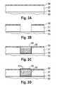
- FIGS. 2 A- 2 Dshows a process sequence for fabrication of a single damascene Cu line illustrating the selective deposition or formation of a metal capping layer by electroless plating.
- dielectric layers 55 - 57 and 58are deposited as shown in FIG. 2A.
- a patternis transferred by lithographic processing into dielectric layers 56 and 57 as shown in FIG. 2B.
- Liner metal 59is then deposited followed by Cu conductor 60 which is thicker than the pattern depth.
- the excess Cu conductor 60 and the liner 59are removed by CMP to form a planar surface as shown in FIG. 2C.
- a thin electroless metal coating 63is deposited selectively onto the Cu conductor 60 as shown in FIG. 2D.
- the process shown in FIGS. 2 A- 2 Dmay be repeated for the next Cu conductor interconnection level.
- FIG. 3is a process sequence for a dual damascene process in which lines and vias of Cu are deposited simultaneously.
- the pattern opening for vias 71are transferred through the dielectric layer 67 as shown in FIG. 3B, then the line or via patterns are transferred as shown in FIG. 3C into layer 67 , during which the via etch for vias 71 continue through dielectric layers 66 and 67 to the previously formed Cu line below (not shown).
- the pattern opening for the lines 70may be transferred first through dielectric layer 67 then the via pattern may be transferred into layer 67 to provide the opening shown in FIG. 3C.
- the liner metal 69is then deposited, Cu is deposited into both patterns, usually by electroplating, and planarized by CMP to provide a structure of lines 70 and vias 71 as shown in FIG. 3D.
- the electroless metal coating 74is then formed on the top surface of line 70 as shown in FIG. 3E. Continuation of the structure to the next level requires repeating the step of forming planer dielectric layers 66 ′ and 67 ′ shown in FIG. 3E.
- the electroless coating 74now separates the Cu surface of line 70 from the planar dielectric 66 ′ formed above.
- the materials used for layers 23 , 27 , 32 , and 37may be used for layers 55 and 57 isn FIGS. 2 A- 2 D and layers 65 and 67 in FIGS. 3 A- 3 E.
- the materials used for layers 26 , 31 , 36 and 42may be used for layer 56 in FIGS. 2 A- 2 D and layer 66 in FIGS. 3 A- 3 E.
- FIG. 4shows a cross section view of a three-level damascene interconnection with a SiNx/SiO2 dielectric.
- a dielectric layer 67has a lower W line 76 connecting through a W via 77 to the lower surface of liner 69 and a first end of Cu conductor 70 .
- Cu conductor 70has liner 69 on three surfaces and has a width of 0.28 ⁇ m.
- Cu conductor 70was electroplated.
- a second end of Cu conductor 70is connected through liner 79 to the lower surface of Cu conductor 80 . Electron current was passed from W line 76 to Cu conductor 80 .
- the upper surface of Cu conductor 70 and dielectric layer 67was planarized by CMP. Then a metal film 74 was formed on the upper surface of Cu conductor 70 .
- a dielectric layer 66 ′ of silicon nitridewas formed on layer 67 and Cu conductor 70 .
- a dielectric layer 67 ′was formed above layer 66 ′.
- a trench and viawas formed in dielectric layer 67 ′ and a liner was formed in trench and via followed by filling with Cu conductor 80 .
- the layer 67 ′ and Cu conductor 80was planarized by CMP.
- Cu condutor 80was chosen to be wide and short to prevent electromigation damage in Cu conductor 80 .
- a layer 82 of silicon nitridewas formed on layer 67 ′ and Cu conductor 80 .
- a dielectric layer 84was formed over layer 82 .
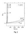
- Test structure 75was tested for electromigration at 294° C. and at 25 mA/mm 2 with various electroless deposited metal coatings 74 and with no coating as shown in FIG. 1.
- FIG. 5shows electromigration testing at 294° C. illustrating the superior lifetimes of Cu lines having a metal liner 69 on three sides and coated with metal layers 74 on the top surface of Cu conductor 70 .
- the ordinaterepresents R/R 0 and the abscissa represents time in hours. Note that the resistance change as a function of time which monitors rate of migration, has not reached normal failure levels of 1.2 in FIG. 5 representing a 20% change in reistance of coated samples even after 20 ⁇ the failure time of uncoated Cu lines.
- FIG. 5illustrates the significant improvement in electromigration lifetime by metal coating 74 .
- the resistance change in Cu conductor 70 in test structure 75is monitored as a means of tracking the degree of Cu atomic migration that is occurring, the higher the resistance change over time the more the Cu atomic transport and the lower the Cu conductor lifetime. As is shown in FIG. 5, the resistance increases catastrophically in the uncoated samples shown by curves 91 - 94 while in all of the coated samples with metal film 74 the resistance change is very slow as shown by curves 97 - 99 . In this test, the normal lifetime was defined as 20% change to its original resistance R 0 , and was not reached until after at least 2200 hours, whereas the Cu line with no top surface coating has failed within 100 hours.
Landscapes
- Engineering & Computer Science (AREA)
- Physics & Mathematics (AREA)
- Condensed Matter Physics & Semiconductors (AREA)
- General Physics & Mathematics (AREA)
- Computer Hardware Design (AREA)
- Microelectronics & Electronic Packaging (AREA)
- Power Engineering (AREA)
- Manufacturing & Machinery (AREA)
- Internal Circuitry In Semiconductor Integrated Circuit Devices (AREA)
- Chemically Coating (AREA)
- Electrodes Of Semiconductors (AREA)
Abstract
Description
- This invention relates to metal interconnections on semiconductor chips and more particularly to a surface coating or treatment to prevent surface atoms of conductors from being moved downstream by an electron current, a phenomena known as electromigration, and/or from being moved by a stress gradient tending to relax stress known as stress induced migration.[0001]
- Increased density and speed of microelectronic circuitry has caused a shift in the metallization system from Al(Cu) to Cu to reduce the resistance of the conductor. At the same time, the need for higher levels of current density has exposed the Al(Cu) lines to failure by electromigration, limiting the extent to which circuit designers can increase performance. The higher melting point of Cu is expected to improve the current carrying capability of the conductors, extending electromigration lifetime. However, from our test results, we have found that the electromigration lifetime is most dependent on the atomic behavior such as atomic transport at the Cu/dielectric interface and not on the intrinsic character of the Cu lattice, grain boundary or Cu/liner interface atom transport. Thus, the specifications for allowed current in Cu conductors proved not to be significantly superior to those for Al(Cu).[0002]
- The basic process for fabricating Cu conductor patterns is by the damascene method where trenches are formed in a dielectric layer, a liner is formed in the trenches and then the trenches are filled with Cu and then chemical mechanical polished (CMP) which terminates in a clean top Cu surface coplanar with the dielectric layer. Cu/metal liner interfaces are formed on the other three surfaces of the Cu conductor. The electromigration lifetime is a function of the line thickness, width and cross section area. Data from measurements showed that only the top surface was contributing to mass transport for Cu conductors with bamboo-like and near bamboo grain structure and a combination of boundary and surface were contributing to mass transport for wider lines. The same relationship was found to be independent of the Cu deposition method, i.e., whether the deposition was by Physical Vapor Deposition (PVD), Chemical Vapor Deposition (CVD) or electroplating, illustrating the pervasiveness of the problem. In addition to electromigration lifetime failure, it was found that Cu conductor patterns are susceptible to atomic voiding under thermal cycle stress, with voids always found to be initiated at the Cu/dielectric interface where the atomic mobility is highest. Since the copper migration rate, drift velocity, is a product of mobility (D/kT) times driving force (F) where D is the diffusivity of Cu, T is the absolute temperature in Kelvin, k is the Boltzmann constant. The driving forces, F, are Z*eE and (Ds/Dx) W for electromigration and stress induced migration forces, respectively, where Z* is the effective charge number, e is the electronic charge, E is the electric field, (Ds/Dx) is the stress gradient, and W is the atomic volume. It is now inevitable that achievement of a Cu conductor technology with which the highest performance and reliability can be realized will require alteration or modification of the Cu/dielectric interface of an overlayer to reduce Cu transport and atomic voiding.[0003]
- Modification of the Cu conductor surface can be done after CMP. Then, the process should be selective to Cu and provide a thin layer on the surface of the Cu conductor so as to remain substantially coplanar with the dielectric or insulation containing the trenches. The process must result in improved adhesion between the Cu conductor and the subsequently formed dielectric over layer and improved oxidation resistance of the Cu atoms in the Cu conductor, as well as reduced atomic transport of the Cu conductor, to provide maximum reliability.[0004]
- In accordance with the present invention, the exposed Cu surface of a Cu conductor is altered by providing a thin metal layer in the range from 1 to 20 nm on the Cu surface, such as subsequent to a CMP planarization or a dry etching process, in order to reduce susceptibility to electromigration, oxidation, corrosion, stress voiding and delamination during subsequent chip processing and/or chip utilization, thus improving reliability and yield. This invention teaches the method of electroless metal deposition as one way to form a thin metal layer on a Cu conductor to increase electromigration lifetime and stress induced migration resistance.[0005]
- The selective deposition process comprises the following steps.[0006]
- a. Selective activation of the copper surface using a Pd ion catalyst which is shown in Equation 1.[0007]
- Cu+Pd++-à Cu+++Pd (1)
- This procedure leaves a multitude of Pd nanoparticles on the surface of the copper lines to act as a catalyst for the next step.[0008]
- b. Selective deposition of a metal or alloy using electroless reduction which is shown in Equation 2.[0009]
- reducing agent+Men++Cu-à Cu/Me+oxidized form of reducing agent (2)
- Where Me[0010]n+ is a metal ion, for example, Co2+.
- For example, using hypophosphite as the reducing agent and cobalt ions as the capping metal, we have a chemical reaction as shown in Equation 3.[0011]
- 2 H2PO2−+Co2++H20 . . . (( . . . Cu . . . ))-à Co+2HP032−+H2+4 H+ (3)
- In the course of this invention we have used the hypophosphite (capping layer) system described above, and deposited onto the surface of the copper conductor the metal palladium, cobalt, cobalt-tungsten, cobalt-tungsten-phosphide, cobalt-tin, cobalt-tin-phosphide, colbalt phosphide and other alloys of cobalt. It is also understood that other reducing agents can be used, such as dimethylamino borane, which allows deposition of other types of alloys, such as Co—B or Ni—B.[0012]
- As a result of steps a and b above, the exposed surface of the copper conductors are coated with a thin film preferably in the range from 1 to 10 nm thick of a metal compound or alloy which is strongly adhered via chemical and/or metalurgical bonds to copper atoms on or in the copper surface.[0013]
- The following important findings are critical to this invention in a damascene process for making copper interconnects on integrated circuit chips.[0014]
- 1. The thickness of the coating film on the copper surface must be small: maximum 20 nm, and preferably between 1 and 10 nm due to damascene process considerations. In this way, at least three major properties are achieved: a) the resistivity of the Cu line is not affected or increased by more than 20%, b) the electrical leakage, which may occur due to bridging between Cu conductors, is eliminated and c) no further planarization of the Cu conductor or line is necessary. Planarization or substantial planarization of the Cu conductor/dielectric surface is required in order to provide a planarized top surface of a subsequently formed dielectric layer thereover without the need to planarized the top surface of the subsequent dielectric layer. Step features from one surface are translated through the next layer to the surface above especially when formed by CVD.[0015]
- 2. The preferred composition of the coating films may be Co—Sn—P, Co—W—P, Co—P or Pd.[0016]
- 3. The wafers with coated films were annealed at 300° C. for two (2) hours to further improve the chemical or metalurgical bonding to the copper surface and slow down diffusion of the copper atoms along the Cu surface at the Cu conductor/dielectric interface and along grain boundaries. The Cu conductor/dielectric interface is between the Cu conductor and the dielectric layer formed over the Cu conductor. The Cu conductor in a damascene process is in a trench in a dielectric layer with a metal liner formed in the trench prior to filling with the Cu conductor.[0017]
- 4. Also, selective CVD of metals, or other deposition processes may be used to deposit a metal film on the surface of the Cu conductor with chemical and/or metalurgical bonding to achieve increased electromigration resistance of the Cu conductor.[0018]
- These and other features, objects, and advantages of the present invention will become apparent upon consideration of the following detailed description of the invention when read in conjunction with the drawing in which:[0019]
- FIG. 1 is a cross section view of one embodiment of the invention.[0020]
- FIGS.[0021]2A-2D are cross section views of stages in the fabrication of a second embodiment of the invention.
- FIGS.[0022]3A-3E are cross section views of stages in fabricating a third embodiment.
- FIG. 4 is a cross section view of a three level electromigration test structure.[0023]
- FIG. 5 is a graph showing the ohmic resistance of a Cu conductor and liner in a trench in a dielectric layer with and without a thin metal film on the top surface versus time.[0024]
- Referring now to the drawing, FIG. 1 is a cross section view of an example of a Cu Back End of the Line (BEOL) structure on an integrated[0025]
circuit chip 10 containing Cu lines and vias produced by a single damascene process. - In FIG. 1,[0026]
integrated circuit chip 10 has asubstrate 11 which may be, for example, Si, SiGe, Ge, SOI and GaAs.Substrate 11 may have formed therein,source 16 and drain17 regions andgate 18 of a typical FET transistor19. On either side ofsource 16 and drain17 regions are recessedoxide regions substrate 11. Alayer 23 of oxide is formed overoxide regions layer 23 and filled withmetal 25 which is usually tungsten.Layer 23 andmetal 25 are planarized by Chemical Mechanical Polishing (CMP). Acapping layer 26 of, for example, silicon nitride is formed on the upper surface oflayer 23.Layer 27 of dielectric is formed onlayer 26 and trenches are formed therein. Aliner 28 is formed on the bottom and sidewalls of trenches and then filled with Cu to formlines 29.Layer 27 andlines 29 are planarized by CMP. Acapping layer 31 is formed on the upper surface oflayer 27 and lines29. Alayer 32 of dielectric is formed on cappinglayer 31. Via openings are formed inlayers metal liner 33 and metal such as Cu in the opening to form via34.Layers 32 and via34 are planarized by CMP. Acapping layer 36 is formed onlayers 32 and via34. A layer37 of dielectric is formed on cappinglayer 36. Trenches or openings are formed in layer37 andcapping layer 36. Aliner 38 is formed in the trenches in layer37 andcapping layer 36. The trenches are filled with Cu metal to formlines 39. Layer37 andlines 39 are planarized by CMP. Acapping layer 42 is formed on layer37 and lines39. Capping layers26,31 and36 are of a different dielectric than the dielectric oflayers lines 31amd 39 are interfaced with dielectric8. - FIGS.[0027]2A-2D shows a process sequence for fabrication of a single damascene Cu line illustrating the selective deposition or formation of a metal capping layer by electroless plating. In the process sequence, dielectric layers55-57 and58 are deposited as shown in FIG. 2A. A pattern is transferred by lithographic processing into
dielectric layers Liner metal 59 is then deposited followed byCu conductor 60 which is thicker than the pattern depth. Theexcess Cu conductor 60 and theliner 59 are removed by CMP to form a planar surface as shown in FIG. 2C. A thinelectroless metal coating 63 is deposited selectively onto theCu conductor 60 as shown in FIG. 2D. The process shown in FIGS.2A-2D may be repeated for the next Cu conductor interconnection level. - FIG. 3 is a process sequence for a dual damascene process in which lines and vias of Cu are deposited simultaneously. Starting from planar dielectric layers[0028]65-67 shown in FIG. 3A, the pattern opening for
vias 71 are transferred through thedielectric layer 67 as shown in FIG. 3B, then the line or via patterns are transferred as shown in FIG. 3C intolayer 67, during which the via etch forvias 71 continue throughdielectric layers lines 70 may be transferred first throughdielectric layer 67 then the via pattern may be transferred intolayer 67 to provide the opening shown in FIG. 3C. Theliner metal 69 is then deposited, Cu is deposited into both patterns, usually by electroplating, and planarized by CMP to provide a structure oflines 70 and vias71 as shown in FIG. 3D. Theelectroless metal coating 74 is then formed on the top surface ofline 70 as shown in FIG. 3E. Continuation of the structure to the next level requires repeating the step of forming planer dielectric layers66′ and67′ shown in FIG. 3E. Theelectroless coating 74 now separates the Cu surface ofline 70 from theplanar dielectric 66′ formed above. The materials used forlayers layers layers layer 56 in FIGS.2A-2D andlayer 66 in FIGS.3A-3E. - In both the single and dual damascene processes shown in FIGS. 2 and 3, the critical improvement in reliability is afforded by the total encompassing or enclosing of the Cu conductor by[0029]
metal layers liner 38 as shown in FIG. 1 and the fourth or top surface ofconductor 39 is shown to be in contact with dielectric, usually cappingdielectric layer 42 which interface is the source of Cu atomic transport and atomic voiding. - The[0030]
test structure 75 shown in FIG. 4 was used for electromigration lifetime measurements. FIG. 4 shows a cross section view of a three-level damascene interconnection with a SiNx/SiO2 dielectric. Adielectric layer 67 has alower W line 76 connecting through a W via77 to the lower surface ofliner 69 and a first end ofCu conductor 70.Cu conductor 70 hasliner 69 on three surfaces and has a width of 0.28 μm.Cu conductor 70 was electroplated. A second end ofCu conductor 70 is connected throughliner 79 to the lower surface of Cu conductor80. Electron current was passed fromW line 76 to Cu conductor80. The upper surface ofCu conductor 70 anddielectric layer 67 was planarized by CMP. Then ametal film 74 was formed on the upper surface ofCu conductor 70. Adielectric layer 66′ of silicon nitride was formed onlayer 67 andCu conductor 70. Adielectric layer 67′ was formed abovelayer 66′. A trench and via was formed indielectric layer 67′ and a liner was formed in trench and via followed by filling with Cu conductor80. Thelayer 67′ and Cu conductor80 was planarized by CMP. Cu condutor80 was chosen to be wide and short to prevent electromigation damage in Cu conductor80. A layer82 of silicon nitride was formed onlayer 67′ and Cu conductor80. Adielectric layer 84 was formed over layer82.Test structure 75 was tested for electromigration at 294° C. and at 25 mA/mm2with various electroless depositedmetal coatings 74 and with no coating as shown in FIG. 1. - FIG. 5 shows electromigration testing at 294° C. illustrating the superior lifetimes of Cu lines having a[0031]
metal liner 69 on three sides and coated withmetal layers 74 on the top surface ofCu conductor 70. In FIG. 5, the ordinate represents R/R0and the abscissa represents time in hours. Note that the resistance change as a function of time which monitors rate of migration, has not reached normal failure levels of 1.2 in FIG. 5 representing a 20% change in reistance of coated samples even after 20× the failure time of uncoated Cu lines. FIG. 5 illustrates the significant improvement in electromigration lifetime bymetal coating 74. The resistance change inCu conductor 70 intest structure 75 is monitored as a means of tracking the degree of Cu atomic migration that is occurring, the higher the resistance change over time the more the Cu atomic transport and the lower the Cu conductor lifetime. As is shown in FIG. 5, the resistance increases catastrophically in the uncoated samples shown by curves91-94 while in all of the coated samples withmetal film 74 the resistance change is very slow as shown by curves97-99. In this test, the normal lifetime was defined as 20% change to its original resistance R0, and was not reached until after at least 2200 hours, whereas the Cu line with no top surface coating has failed within 100 hours. The lowest rate of change is found withcoating 74 of CoWP shown bycurve 97, but all of thecoatings 74 of CoSnP shown bycurve 98 and Pd shown bycurve 99 provided similarly long lifetimes. It is expected that extrapolation of the improvement to use temperatures 100° C. would give more than two orders of magnitude increase in electromigration and stress migration lifetime, which translates to exceptional flexibility for the circuit designers and effectively removes electromigration as the limiting factor for use current. It was also found with the same set of coated samples that atomic stress voiding was not observed under thermal cycle conditions that produced voiding in the standard uncoated samples. The results of this testing further supports the hypothesis that the uncoated surfaces, or interfaces of Cu with dielectric, are the major sources of electromigration and thus reliability degradation. - While there has been described and illustrated a structure and method for improving the electromigration resistance and reducing the stress induced migration in a Cu conductor by forming a conductive film having metal to metal chemical and metallurgical bonding on and to the upper surface of the Cu conductor, it will be apparent to those skilled in the art that modifications and variations are possible without deviating from the broad scope of the invention which shall be limited solely by the scope of the claims appended hereto.[0032]
Claims (36)
1. A method for forming conductors with high electromigration resistance comprising the steps of
forming a layer of dielectric on a substrate,
forming at least one trench in said layer of dielectric,
forming a metal liner in said trench,
forming a conductor on said metal liner filling said trench,
forming a planarized upper surface of said conductor planar with the upper surface of said layer of dielectric, and
forming a conductive film over said upper surface of said conductor, said conductive film forming a metal to metal metallurgical bond.
2. The method ofclaim 1 wherein said step of forming a conductive film includes the step of forming said conductive film by electroless deposition whereby said upper surface of said conductor is protected from oxidation and corrosion and provides high electromigration resistance and high resistance to thermal stress voiding.
3. The method ofclaim 2 wherein said electroless deposited film has a thickness in the range of 1 to 20 nanometers.
4. The method ofclaim 2 wherein said electroless deposited film has a thickness in the range of 1 to 10 nanometers.
5. The method ofclaim 2 wherein said step of electroless deposition includes the steps of first immersing said substrate in a solution of metal ions whereby a layer of nanoparticles of metal are formed on said upper surface of said conductor,
second immersing said substrate in an electroless complexed solution of metal ions and hypophosphite ions whereby a metal-phosphide conductive film is formed on said upper surface of said conductor, and
annealing said substrate in one of an inert and reducing atmosphere at a temperature of at least 300° C. for at least 2 hours whereby excellent adhesion is obtained between said conductor and said metal phosphide-conductive film.
6. The method ofclaim 5 wherein said step of second immersing is omitted.
7. The method ofclaim 5 wherein said conductive film is selected from the group consisting of CoWP, CoSnP, CoP, Pd, In and W and is in the range from 1 to 20 nm thick.
8. The method ofclaim 2 wherein said step of electroless deposition includes the steps of first immersing said substrate in a solution of metal ions whereby a layer of nanoparticles of metal are formed on the surface of said conductor,
second immersing said substrate in an electroless complexed solution of metal ions and dimethylamino borane whereby a layer of metal-boron conductive film is formed on said upper surface of said conductor, and
annealing said substrate in one of an inert and reducing atmosphere at a temperature of at least 300° C. for at least 2 hours whereby excellent adhesion is obtained between said conductor and said metal boron conductive film.
9. The method ofclaim 1 wherein said conductive film is applied on the surface of said conductor by physical methods such as Chemical Vapor Deposition (CVD), Physical Vapor Deposition (PVD), evaporation, sputtering and thermal metal interdiffusion.
10. The method ofclaim 9 wherein said conductive film is selected from the group consisting of Pd, In, W and mixtures thereof.
11. A structure comprising:
a layer of dielectric on a substrate,
at least one trench formed in said dielectric on said substrate,
a metal liner formed in said trench,
a conductor on said liner filling said trench,
a planarized upper surface of said conductor with the upper surface of said layer of dielectric, and
a conductive film over said upper surface of said conductor, said conductive film forming a metal to metal chemical and metallurgical bond.
12. The structure ofclaim 11 wherein said conductive film is selected from the group consisting of CoWP, CoSnP, CoP, Pd, CoB, CoSnB, CoWB, In, NiB and W whereby said upper surface of said conductor is protected from oxidation and corrosion.
13. The structure ofclaim 12 wherein said conductive film has a thickness in the range of 1 to 20 nm.
14. The structure ofclaim 12 further including an insulating cap dielectric layer over said conductive film on said conductor and said layer of dielectric.
15. The structure ofclaim 14 wherein said insulating dielectric cap layer is selected from the group consisting of silicon nitride, silicon oxide, insulating compounds of SICOH having dielectric constants less than 3.2, diamond-like carbon, fluorinated diamond like carbon and poly (Arylene ether).
16. The structure ofclaim 11 wherein said conductor is selected from the group consisting of copper and copper alloys.
17. The structure ofclaim 11 wherein said susbtrate is chosen from the group of silicon, silicon-germanium, SOI, and gallium arsenide.
18. A method for forming conductors with high electromigration resistance comprising the steps of
forming a patterned conductor on a substrate,
forming a conductive film over said surface of said conductor, said conductive film forming a metal to metal metallurgical bond.
19. The method ofclaim 18 wherein said step of forming a conductive film includes the step of forming said conductive film by electroless deposition whereby said surface of said conductor is protected from oxidation and corrosion and provides high electromigration resistance and high resistance to thermal stress voiding.
20. The method ofclaim 19 wherein said electroless deposited film has a thickness in the range of 1 to 20 nanometers.
21. The method ofclaim 19 wherein said electroless deposited film has a thickness in the range of 1 to 10 nanometers.
22. The method ofclaim 19 wherein said step of electroless deposition includes the steps of first immersing said substrate in a solution of metal ions whereby a layer of nanoparticles of metal are formed on said surface of said conductor,
second immersing said substrate in an electroless complexed solution of metal ions and hypophosphite ions whereby a metal-phosphide conductive film is formed on said surface of said conductor, and
annealing said substrate in one of an inert and reducing atmosphere at a temperature of at least 300° C. for at least 2 hours whereby excellent adhesion is obtained between said conductor and said metal phosphide conductive film.
23. The method ofclaim 22 wherein said step of second immersing is omitted.
24. The method ofclaim 22 wherein said conductive film is selected from the group consisting of CoWP, CoSnP, CoP, Pd, In and W and is in the range from 1 to 20 nm thick.
25. The method ofclaim 19 wherein said step of electroless deposition includes the steps of first immersing said substrate in a solution of metal ions whereby a layer of nanoparticles of metal are formed on the surface of said conductor,
second immersing said substrate in an electroless complexed solution of metal ions and dimethylamino borane whereby a layer of metal-boron conductive film is formed on said surface of said conductor, and
annealing said substrate in one of an inert and reducing atmosphere at a temperature of at least 300° C. for at least 2 hours whereby excellent adhesion is obtained between said conductor and said metal boron conductive film.
26. The method ofclaim 18 wherein said conductive film is applied on the surface of said conductor by physical methods such as Chemical Vapor Deposition (CVD), Physical Vapor Deposition (PVD), evaporation, sputtering and thermal metal interdiffusion.
27. The method ofclaim 26 wherein said conductive film is selected from the group consisting of Pd, In, W and mixtures thereof.
28. A structure comprising:
a patterned conductor on a substrate,
a conductive film over said surface of said conductor, said conductive film forming a metal to metal metallurgical bond.
29. The structure ofclaim 28 wherein said conductive film is selected from the group consisting of CoWP, CoSnP, CoP, Pd, CoB, CoSnB, CoWB, In, NiB and W whereby said upper surface of said conductor is protected from oxidation and corrosion.
30. The structure ofclaim 29 wherein said conductive film has a thickness in the range of 1 to 20 nm.
31. The structure ofclaim 29 further including an insulating cap dielectric layer over said conductive film on said conductor.
32. The structure ofclaim 31 wherein said insulating dielectric cap layer is selected from the group consisting of silicon nitride, silicon oxide, insulating compounds of SICOH having dielectric constants less than 3.2, diamond-like carbon, fluorinated diamond like carbon and poly (Arylene ether).
33. The structure ofclaim 29 wherein said conductor is selected from the group consisting of copper and copper alloys.
34. The structure ofclaim 29 wherein said susbtrate is chosen from the group of silicon, silicon-germanium, SOI, and gallium arsenide.
35. The method ofclaim 8 wherein said conductive film is selected from the group consisting of CoB, CoSnB, CoWB and NiB.
36. The method ofclaim 25 wherein said conductive film is selected from the group consisting of CoB, CoSnB, CoWB and NiB.
Priority Applications (3)
| Application Number | Priority Date | Filing Date | Title |
|---|---|---|---|
| US10/054,605US20020098681A1 (en) | 1999-07-27 | 2001-11-13 | Reduced electromigration and stressed induced migration of Cu wires by surface coating |
| US11/183,773US7468320B2 (en) | 1999-07-27 | 2005-07-19 | Reduced electromigration and stressed induced migration of copper wires by surface coating |
| US12/341,856US20090142924A1 (en) | 1999-07-27 | 2008-12-22 | Reduced electromigration and stressed induced migration of cu wires by surface coating |
Applications Claiming Priority (2)
| Application Number | Priority Date | Filing Date | Title |
|---|---|---|---|
| US09/361,573US6342733B1 (en) | 1999-07-27 | 1999-07-27 | Reduced electromigration and stressed induced migration of Cu wires by surface coating |
| US10/054,605US20020098681A1 (en) | 1999-07-27 | 2001-11-13 | Reduced electromigration and stressed induced migration of Cu wires by surface coating |
Related Parent Applications (1)
| Application Number | Title | Priority Date | Filing Date |
|---|---|---|---|
| US09/361,573DivisionUS6342733B1 (en) | 1999-07-27 | 1999-07-27 | Reduced electromigration and stressed induced migration of Cu wires by surface coating |
Related Child Applications (1)
| Application Number | Title | Priority Date | Filing Date |
|---|---|---|---|
| US11/183,773ContinuationUS7468320B2 (en) | 1999-07-27 | 2005-07-19 | Reduced electromigration and stressed induced migration of copper wires by surface coating |
Publications (1)
| Publication Number | Publication Date |
|---|---|
| US20020098681A1true US20020098681A1 (en) | 2002-07-25 |
Family
ID=23422581
Family Applications (4)
| Application Number | Title | Priority Date | Filing Date |
|---|---|---|---|
| US09/361,573Expired - LifetimeUS6342733B1 (en) | 1999-07-27 | 1999-07-27 | Reduced electromigration and stressed induced migration of Cu wires by surface coating |
| US10/054,605AbandonedUS20020098681A1 (en) | 1999-07-27 | 2001-11-13 | Reduced electromigration and stressed induced migration of Cu wires by surface coating |
| US11/183,773Expired - LifetimeUS7468320B2 (en) | 1999-07-27 | 2005-07-19 | Reduced electromigration and stressed induced migration of copper wires by surface coating |
| US12/341,856AbandonedUS20090142924A1 (en) | 1999-07-27 | 2008-12-22 | Reduced electromigration and stressed induced migration of cu wires by surface coating |
Family Applications Before (1)
| Application Number | Title | Priority Date | Filing Date |
|---|---|---|---|
| US09/361,573Expired - LifetimeUS6342733B1 (en) | 1999-07-27 | 1999-07-27 | Reduced electromigration and stressed induced migration of Cu wires by surface coating |
Family Applications After (2)
| Application Number | Title | Priority Date | Filing Date |
|---|---|---|---|
| US11/183,773Expired - LifetimeUS7468320B2 (en) | 1999-07-27 | 2005-07-19 | Reduced electromigration and stressed induced migration of copper wires by surface coating |
| US12/341,856AbandonedUS20090142924A1 (en) | 1999-07-27 | 2008-12-22 | Reduced electromigration and stressed induced migration of cu wires by surface coating |
Country Status (7)
| Country | Link |
|---|---|
| US (4) | US6342733B1 (en) |
| EP (1) | EP1210732A1 (en) |
| JP (1) | JP2003505882A (en) |
| KR (1) | KR100496711B1 (en) |
| CN (1) | CN1191621C (en) |
| TW (1) | TW483137B (en) |
| WO (1) | WO2001008213A1 (en) |
Cited By (191)
| Publication number | Priority date | Publication date | Assignee | Title |
|---|---|---|---|---|
| US20030190812A1 (en)* | 2002-04-03 | 2003-10-09 | Deenesh Padhi | Electroless deposition method |
| US20030190426A1 (en)* | 2002-04-03 | 2003-10-09 | Deenesh Padhi | Electroless deposition method |
| US20030189026A1 (en)* | 2002-04-03 | 2003-10-09 | Deenesh Padhi | Electroless deposition method |
| US20040002212A1 (en)* | 2002-06-29 | 2004-01-01 | Hynix Semiconductor Inc. | Method for forming copper metal line in semiconductor device |
| US20040087141A1 (en)* | 2002-10-30 | 2004-05-06 | Applied Materials, Inc. | Post rinse to improve selective deposition of electroless cobalt on copper for ULSI application |
| US20040106219A1 (en)* | 2002-08-19 | 2004-06-03 | Kabushiki Kaisha Toshiba | Method of accelerating test of semiconductor device |
| US20040113277A1 (en)* | 2002-12-11 | 2004-06-17 | Chiras Stefanie Ruth | Formation of aligned capped metal lines and interconnections in multilevel semiconductor structures |
| US20050081785A1 (en)* | 2003-10-15 | 2005-04-21 | Applied Materials, Inc. | Apparatus for electroless deposition |
| US20050095830A1 (en)* | 2003-10-17 | 2005-05-05 | Applied Materials, Inc. | Selective self-initiating electroless capping of copper with cobalt-containing alloys |
| US20050101130A1 (en)* | 2003-11-07 | 2005-05-12 | Applied Materials, Inc. | Method and tool of chemical doping CoW alloys with Re for increasing barrier properties of electroless capping layers for IC Cu interconnects |
| WO2005045923A1 (en)* | 2003-10-27 | 2005-05-19 | Intel Corporation | A method for making a semiconductor device having increased conductive material reliability |
| US20050124158A1 (en)* | 2003-10-15 | 2005-06-09 | Lopatin Sergey D. | Silver under-layers for electroless cobalt alloys |
| US20050136193A1 (en)* | 2003-10-17 | 2005-06-23 | Applied Materials, Inc. | Selective self-initiating electroless capping of copper with cobalt-containing alloys |
| US20050164497A1 (en)* | 2004-01-26 | 2005-07-28 | Sergey Lopatin | Pretreatment for electroless deposition |
| US20050161338A1 (en)* | 2004-01-26 | 2005-07-28 | Applied Materials, Inc. | Electroless cobalt alloy deposition process |
| US20050170650A1 (en)* | 2004-01-26 | 2005-08-04 | Hongbin Fang | Electroless palladium nitrate activation prior to cobalt-alloy deposition |
| US20050181226A1 (en)* | 2004-01-26 | 2005-08-18 | Applied Materials, Inc. | Method and apparatus for selectively changing thin film composition during electroless deposition in a single chamber |
| US20050253268A1 (en)* | 2004-04-22 | 2005-11-17 | Shao-Ta Hsu | Method and structure for improving adhesion between intermetal dielectric layer and cap layer |
| US20050260345A1 (en)* | 2003-10-06 | 2005-11-24 | Applied Materials, Inc. | Apparatus for electroless deposition of metals onto semiconductor substrates |
| US20050263066A1 (en)* | 2004-01-26 | 2005-12-01 | Dmitry Lubomirsky | Apparatus for electroless deposition of metals onto semiconductor substrates |
| US20060001160A1 (en)* | 2003-05-16 | 2006-01-05 | Wen-Kai Wan | Surface treatment of metal interconnect lines |
| US20060003570A1 (en)* | 2003-12-02 | 2006-01-05 | Arulkumar Shanmugasundram | Method and apparatus for electroless capping with vapor drying |
| US20060240187A1 (en)* | 2005-01-27 | 2006-10-26 | Applied Materials, Inc. | Deposition of an intermediate catalytic layer on a barrier layer for copper metallization |
| US20060246699A1 (en)* | 2005-03-18 | 2006-11-02 | Weidman Timothy W | Process for electroless copper deposition on a ruthenium seed |
| US20060251800A1 (en)* | 2005-03-18 | 2006-11-09 | Weidman Timothy W | Contact metallization scheme using a barrier layer over a silicide layer |
| US20060264043A1 (en)* | 2005-03-18 | 2006-11-23 | Stewart Michael P | Electroless deposition process on a silicon contact |
| US7148079B1 (en)* | 2002-11-01 | 2006-12-12 | Advanced Micro Devices, Inc. | Diamond like carbon silicon on insulator substrates and methods of fabrication thereof |
| US20060278123A1 (en)* | 2003-05-09 | 2006-12-14 | Basf Aktiengesellschaft | Composition for the currentless deposition of ternary materials for use in the semiconductor industry |
| US20070071888A1 (en)* | 2005-09-21 | 2007-03-29 | Arulkumar Shanmugasundram | Method and apparatus for forming device features in an integrated electroless deposition system |
| US20070111519A1 (en)* | 2003-10-15 | 2007-05-17 | Applied Materials, Inc. | Integrated electroless deposition system |
| US20070134913A1 (en)* | 2005-12-14 | 2007-06-14 | Semiconductor Manufacturing International (Shanghai) Corporation | Method to eliminate Cu dislocation for reliability and yield |
| US20080120580A1 (en)* | 2006-11-22 | 2008-05-22 | International Business Machines Corporation | Design Structures Incorporating Interconnect Structures with Improved Electromigration Resistance |
| US20090087983A1 (en)* | 2007-09-28 | 2009-04-02 | Applied Materials, Inc. | Aluminum contact integration on cobalt silicide junction |
| US20090111280A1 (en)* | 2004-02-26 | 2009-04-30 | Applied Materials, Inc. | Method for removing oxides |
| US20090236745A1 (en)* | 2008-03-24 | 2009-09-24 | Air Products And Chemicals, Inc. | Adhesion to Copper and Copper Electromigration Resistance |
| US7651934B2 (en) | 2005-03-18 | 2010-01-26 | Applied Materials, Inc. | Process for electroless copper deposition |
| KR101016341B1 (en) | 2004-04-30 | 2011-02-22 | 매그나칩 반도체 유한회사 | Inductor manufacturing method of semiconductor device |
| CN102544131A (en)* | 2012-03-12 | 2012-07-04 | 谢振华 | Improved electrode structure for solar battery panel |
| CN103135819A (en)* | 2011-11-29 | 2013-06-05 | 迎辉科技股份有限公司 | Conductive substrate with oxidation resistant metal layer |
| US8679982B2 (en) | 2011-08-26 | 2014-03-25 | Applied Materials, Inc. | Selective suppression of dry-etch rate of materials containing both silicon and oxygen |
| US8679983B2 (en) | 2011-09-01 | 2014-03-25 | Applied Materials, Inc. | Selective suppression of dry-etch rate of materials containing both silicon and nitrogen |
| US8765574B2 (en) | 2012-11-09 | 2014-07-01 | Applied Materials, Inc. | Dry etch process |
| US8771539B2 (en) | 2011-02-22 | 2014-07-08 | Applied Materials, Inc. | Remotely-excited fluorine and water vapor etch |
| US8801952B1 (en) | 2013-03-07 | 2014-08-12 | Applied Materials, Inc. | Conformal oxide dry etch |
| US8808563B2 (en) | 2011-10-07 | 2014-08-19 | Applied Materials, Inc. | Selective etch of silicon by way of metastable hydrogen termination |
| US8895449B1 (en) | 2013-05-16 | 2014-11-25 | Applied Materials, Inc. | Delicate dry clean |
| US8921234B2 (en) | 2012-12-21 | 2014-12-30 | Applied Materials, Inc. | Selective titanium nitride etching |
| US8927390B2 (en) | 2011-09-26 | 2015-01-06 | Applied Materials, Inc. | Intrench profile |
| US8951429B1 (en) | 2013-10-29 | 2015-02-10 | Applied Materials, Inc. | Tungsten oxide processing |
| US8956980B1 (en) | 2013-09-16 | 2015-02-17 | Applied Materials, Inc. | Selective etch of silicon nitride |
| US8969212B2 (en) | 2012-11-20 | 2015-03-03 | Applied Materials, Inc. | Dry-etch selectivity |
| US8975152B2 (en) | 2011-11-08 | 2015-03-10 | Applied Materials, Inc. | Methods of reducing substrate dislocation during gapfill processing |
| US8980763B2 (en) | 2012-11-30 | 2015-03-17 | Applied Materials, Inc. | Dry-etch for selective tungsten removal |
| US8999856B2 (en) | 2011-03-14 | 2015-04-07 | Applied Materials, Inc. | Methods for etch of sin films |
| US9023734B2 (en) | 2012-09-18 | 2015-05-05 | Applied Materials, Inc. | Radical-component oxide etch |
| US9023732B2 (en) | 2013-03-15 | 2015-05-05 | Applied Materials, Inc. | Processing systems and methods for halide scavenging |
| US9034770B2 (en) | 2012-09-17 | 2015-05-19 | Applied Materials, Inc. | Differential silicon oxide etch |
| US9040422B2 (en) | 2013-03-05 | 2015-05-26 | Applied Materials, Inc. | Selective titanium nitride removal |
| US9064816B2 (en) | 2012-11-30 | 2015-06-23 | Applied Materials, Inc. | Dry-etch for selective oxidation removal |
| US9064815B2 (en) | 2011-03-14 | 2015-06-23 | Applied Materials, Inc. | Methods for etch of metal and metal-oxide films |
| US9111877B2 (en) | 2012-12-18 | 2015-08-18 | Applied Materials, Inc. | Non-local plasma oxide etch |
| US9117855B2 (en) | 2013-12-04 | 2015-08-25 | Applied Materials, Inc. | Polarity control for remote plasma |
| US9114438B2 (en) | 2013-05-21 | 2015-08-25 | Applied Materials, Inc. | Copper residue chamber clean |
| US9132436B2 (en) | 2012-09-21 | 2015-09-15 | Applied Materials, Inc. | Chemical control features in wafer process equipment |
| US9136273B1 (en) | 2014-03-21 | 2015-09-15 | Applied Materials, Inc. | Flash gate air gap |
| US9159606B1 (en) | 2014-07-31 | 2015-10-13 | Applied Materials, Inc. | Metal air gap |
| US9165786B1 (en) | 2014-08-05 | 2015-10-20 | Applied Materials, Inc. | Integrated oxide and nitride recess for better channel contact in 3D architectures |
| US9190293B2 (en) | 2013-12-18 | 2015-11-17 | Applied Materials, Inc. | Even tungsten etch for high aspect ratio trenches |
| US9236266B2 (en) | 2011-08-01 | 2016-01-12 | Applied Materials, Inc. | Dry-etch for silicon-and-carbon-containing films |
| US9236265B2 (en) | 2013-11-04 | 2016-01-12 | Applied Materials, Inc. | Silicon germanium processing |
| US9245762B2 (en) | 2013-12-02 | 2016-01-26 | Applied Materials, Inc. | Procedure for etch rate consistency |
| US9263278B2 (en) | 2013-12-17 | 2016-02-16 | Applied Materials, Inc. | Dopant etch selectivity control |
| US9269590B2 (en) | 2014-04-07 | 2016-02-23 | Applied Materials, Inc. | Spacer formation |
| US9287134B2 (en) | 2014-01-17 | 2016-03-15 | Applied Materials, Inc. | Titanium oxide etch |
| US9287095B2 (en) | 2013-12-17 | 2016-03-15 | Applied Materials, Inc. | Semiconductor system assemblies and methods of operation |
| US9293568B2 (en) | 2014-01-27 | 2016-03-22 | Applied Materials, Inc. | Method of fin patterning |
| US9299537B2 (en) | 2014-03-20 | 2016-03-29 | Applied Materials, Inc. | Radial waveguide systems and methods for post-match control of microwaves |
| US9299583B1 (en) | 2014-12-05 | 2016-03-29 | Applied Materials, Inc. | Aluminum oxide selective etch |
| US9299575B2 (en) | 2014-03-17 | 2016-03-29 | Applied Materials, Inc. | Gas-phase tungsten etch |
| US9299538B2 (en) | 2014-03-20 | 2016-03-29 | Applied Materials, Inc. | Radial waveguide systems and methods for post-match control of microwaves |
| US9309598B2 (en) | 2014-05-28 | 2016-04-12 | Applied Materials, Inc. | Oxide and metal removal |
| US9324576B2 (en) | 2010-05-27 | 2016-04-26 | Applied Materials, Inc. | Selective etch for silicon films |
| US9343272B1 (en) | 2015-01-08 | 2016-05-17 | Applied Materials, Inc. | Self-aligned process |
| US9349605B1 (en) | 2015-08-07 | 2016-05-24 | Applied Materials, Inc. | Oxide etch selectivity systems and methods |
| US9355862B2 (en) | 2014-09-24 | 2016-05-31 | Applied Materials, Inc. | Fluorine-based hardmask removal |
| US9355856B2 (en) | 2014-09-12 | 2016-05-31 | Applied Materials, Inc. | V trench dry etch |
| US9362130B2 (en) | 2013-03-01 | 2016-06-07 | Applied Materials, Inc. | Enhanced etching processes using remote plasma sources |
| US9368364B2 (en) | 2014-09-24 | 2016-06-14 | Applied Materials, Inc. | Silicon etch process with tunable selectivity to SiO2 and other materials |
| US9373517B2 (en) | 2012-08-02 | 2016-06-21 | Applied Materials, Inc. | Semiconductor processing with DC assisted RF power for improved control |
| US9373522B1 (en) | 2015-01-22 | 2016-06-21 | Applied Mateials, Inc. | Titanium nitride removal |
| US9378978B2 (en) | 2014-07-31 | 2016-06-28 | Applied Materials, Inc. | Integrated oxide recess and floating gate fin trimming |
| US9378969B2 (en) | 2014-06-19 | 2016-06-28 | Applied Materials, Inc. | Low temperature gas-phase carbon removal |
| US9385028B2 (en) | 2014-02-03 | 2016-07-05 | Applied Materials, Inc. | Air gap process |
| US9390937B2 (en) | 2012-09-20 | 2016-07-12 | Applied Materials, Inc. | Silicon-carbon-nitride selective etch |
| US9396989B2 (en) | 2014-01-27 | 2016-07-19 | Applied Materials, Inc. | Air gaps between copper lines |
| US9406523B2 (en) | 2014-06-19 | 2016-08-02 | Applied Materials, Inc. | Highly selective doped oxide removal method |
| US9425058B2 (en) | 2014-07-24 | 2016-08-23 | Applied Materials, Inc. | Simplified litho-etch-litho-etch process |
| US9449846B2 (en) | 2015-01-28 | 2016-09-20 | Applied Materials, Inc. | Vertical gate separation |
| US9472417B2 (en) | 2013-11-12 | 2016-10-18 | Applied Materials, Inc. | Plasma-free metal etch |
| US9478432B2 (en) | 2014-09-25 | 2016-10-25 | Applied Materials, Inc. | Silicon oxide selective removal |
| US9493879B2 (en) | 2013-07-12 | 2016-11-15 | Applied Materials, Inc. | Selective sputtering for pattern transfer |
| US9496167B2 (en) | 2014-07-31 | 2016-11-15 | Applied Materials, Inc. | Integrated bit-line airgap formation and gate stack post clean |
| US9499898B2 (en) | 2014-03-03 | 2016-11-22 | Applied Materials, Inc. | Layered thin film heater and method of fabrication |
| US9502258B2 (en) | 2014-12-23 | 2016-11-22 | Applied Materials, Inc. | Anisotropic gap etch |
| US9553102B2 (en) | 2014-08-19 | 2017-01-24 | Applied Materials, Inc. | Tungsten separation |
| US9576809B2 (en) | 2013-11-04 | 2017-02-21 | Applied Materials, Inc. | Etch suppression with germanium |
| US9659753B2 (en) | 2014-08-07 | 2017-05-23 | Applied Materials, Inc. | Grooved insulator to reduce leakage current |
| US9691645B2 (en) | 2015-08-06 | 2017-06-27 | Applied Materials, Inc. | Bolted wafer chuck thermal management systems and methods for wafer processing systems |
| US9721789B1 (en) | 2016-10-04 | 2017-08-01 | Applied Materials, Inc. | Saving ion-damaged spacers |
| US9728437B2 (en) | 2015-02-03 | 2017-08-08 | Applied Materials, Inc. | High temperature chuck for plasma processing systems |
| US9741593B2 (en) | 2015-08-06 | 2017-08-22 | Applied Materials, Inc. | Thermal management systems and methods for wafer processing systems |
| US9768034B1 (en) | 2016-11-11 | 2017-09-19 | Applied Materials, Inc. | Removal methods for high aspect ratio structures |
| US9773648B2 (en) | 2013-08-30 | 2017-09-26 | Applied Materials, Inc. | Dual discharge modes operation for remote plasma |
| US9847289B2 (en) | 2014-05-30 | 2017-12-19 | Applied Materials, Inc. | Protective via cap for improved interconnect performance |
| US9865484B1 (en) | 2016-06-29 | 2018-01-09 | Applied Materials, Inc. | Selective etch using material modification and RF pulsing |
| US9881805B2 (en) | 2015-03-02 | 2018-01-30 | Applied Materials, Inc. | Silicon selective removal |
| US9885117B2 (en) | 2014-03-31 | 2018-02-06 | Applied Materials, Inc. | Conditioned semiconductor system parts |
| US9929050B2 (en)* | 2013-07-16 | 2018-03-27 | Taiwan Semiconductor Manufacturing Company, Ltd. | Mechanisms for forming three-dimensional integrated circuit (3DIC) stacking structure |
| US9934942B1 (en) | 2016-10-04 | 2018-04-03 | Applied Materials, Inc. | Chamber with flow-through source |
| US9947549B1 (en) | 2016-10-10 | 2018-04-17 | Applied Materials, Inc. | Cobalt-containing material removal |
| US10026621B2 (en) | 2016-11-14 | 2018-07-17 | Applied Materials, Inc. | SiN spacer profile patterning |
| US10043684B1 (en) | 2017-02-06 | 2018-08-07 | Applied Materials, Inc. | Self-limiting atomic thermal etching systems and methods |
| US10043674B1 (en) | 2017-08-04 | 2018-08-07 | Applied Materials, Inc. | Germanium etching systems and methods |
| US10049891B1 (en) | 2017-05-31 | 2018-08-14 | Applied Materials, Inc. | Selective in situ cobalt residue removal |
| US10062579B2 (en) | 2016-10-07 | 2018-08-28 | Applied Materials, Inc. | Selective SiN lateral recess |
| US10062585B2 (en) | 2016-10-04 | 2018-08-28 | Applied Materials, Inc. | Oxygen compatible plasma source |
| US10062587B2 (en) | 2012-07-18 | 2018-08-28 | Applied Materials, Inc. | Pedestal with multi-zone temperature control and multiple purge capabilities |
| US10062575B2 (en) | 2016-09-09 | 2018-08-28 | Applied Materials, Inc. | Poly directional etch by oxidation |
| US10128086B1 (en) | 2017-10-24 | 2018-11-13 | Applied Materials, Inc. | Silicon pretreatment for nitride removal |
| US10163696B2 (en) | 2016-11-11 | 2018-12-25 | Applied Materials, Inc. | Selective cobalt removal for bottom up gapfill |
| US10170336B1 (en) | 2017-08-04 | 2019-01-01 | Applied Materials, Inc. | Methods for anisotropic control of selective silicon removal |
| US10170282B2 (en) | 2013-03-08 | 2019-01-01 | Applied Materials, Inc. | Insulated semiconductor faceplate designs |
| US10224210B2 (en) | 2014-12-09 | 2019-03-05 | Applied Materials, Inc. | Plasma processing system with direct outlet toroidal plasma source |
| US10242908B2 (en) | 2016-11-14 | 2019-03-26 | Applied Materials, Inc. | Airgap formation with damage-free copper |
| US10256079B2 (en) | 2013-02-08 | 2019-04-09 | Applied Materials, Inc. | Semiconductor processing systems having multiple plasma configurations |
| US10256112B1 (en) | 2017-12-08 | 2019-04-09 | Applied Materials, Inc. | Selective tungsten removal |
| US10283321B2 (en) | 2011-01-18 | 2019-05-07 | Applied Materials, Inc. | Semiconductor processing system and methods using capacitively coupled plasma |
| US10283324B1 (en) | 2017-10-24 | 2019-05-07 | Applied Materials, Inc. | Oxygen treatment for nitride etching |
| US10297458B2 (en) | 2017-08-07 | 2019-05-21 | Applied Materials, Inc. | Process window widening using coated parts in plasma etch processes |
| US10319649B2 (en) | 2017-04-11 | 2019-06-11 | Applied Materials, Inc. | Optical emission spectroscopy (OES) for remote plasma monitoring |
| US10319739B2 (en) | 2017-02-08 | 2019-06-11 | Applied Materials, Inc. | Accommodating imperfectly aligned memory holes |
| US10319600B1 (en) | 2018-03-12 | 2019-06-11 | Applied Materials, Inc. | Thermal silicon etch |
| US10354889B2 (en) | 2017-07-17 | 2019-07-16 | Applied Materials, Inc. | Non-halogen etching of silicon-containing materials |
| US10403507B2 (en) | 2017-02-03 | 2019-09-03 | Applied Materials, Inc. | Shaped etch profile with oxidation |
| US10431429B2 (en) | 2017-02-03 | 2019-10-01 | Applied Materials, Inc. | Systems and methods for radial and azimuthal control of plasma uniformity |
| US10468267B2 (en) | 2017-05-31 | 2019-11-05 | Applied Materials, Inc. | Water-free etching methods |
| US10490406B2 (en) | 2018-04-10 | 2019-11-26 | Appled Materials, Inc. | Systems and methods for material breakthrough |
| US10490418B2 (en) | 2014-10-14 | 2019-11-26 | Applied Materials, Inc. | Systems and methods for internal surface conditioning assessment in plasma processing equipment |
| US10497573B2 (en) | 2018-03-13 | 2019-12-03 | Applied Materials, Inc. | Selective atomic layer etching of semiconductor materials |
| US10504754B2 (en) | 2016-05-19 | 2019-12-10 | Applied Materials, Inc. | Systems and methods for improved semiconductor etching and component protection |
| US10504700B2 (en) | 2015-08-27 | 2019-12-10 | Applied Materials, Inc. | Plasma etching systems and methods with secondary plasma injection |
| US10522371B2 (en) | 2016-05-19 | 2019-12-31 | Applied Materials, Inc. | Systems and methods for improved semiconductor etching and component protection |
| US10541246B2 (en) | 2017-06-26 | 2020-01-21 | Applied Materials, Inc. | 3D flash memory cells which discourage cross-cell electrical tunneling |
| US10541184B2 (en) | 2017-07-11 | 2020-01-21 | Applied Materials, Inc. | Optical emission spectroscopic techniques for monitoring etching |
| US10546729B2 (en) | 2016-10-04 | 2020-01-28 | Applied Materials, Inc. | Dual-channel showerhead with improved profile |
| US10566206B2 (en) | 2016-12-27 | 2020-02-18 | Applied Materials, Inc. | Systems and methods for anisotropic material breakthrough |
| US10573496B2 (en) | 2014-12-09 | 2020-02-25 | Applied Materials, Inc. | Direct outlet toroidal plasma source |
| US10573527B2 (en) | 2018-04-06 | 2020-02-25 | Applied Materials, Inc. | Gas-phase selective etching systems and methods |
| US10593560B2 (en) | 2018-03-01 | 2020-03-17 | Applied Materials, Inc. | Magnetic induction plasma source for semiconductor processes and equipment |
| US10593523B2 (en) | 2014-10-14 | 2020-03-17 | Applied Materials, Inc. | Systems and methods for internal surface conditioning in plasma processing equipment |
| US10600858B2 (en) | 2018-04-10 | 2020-03-24 | Samsung Display Co., Ltd. | Organic light-emitting display device and method of manufacturing the same |
| US10615047B2 (en) | 2018-02-28 | 2020-04-07 | Applied Materials, Inc. | Systems and methods to form airgaps |
| US10629473B2 (en) | 2016-09-09 | 2020-04-21 | Applied Materials, Inc. | Footing removal for nitride spacer |
| US10672642B2 (en) | 2018-07-24 | 2020-06-02 | Applied Materials, Inc. | Systems and methods for pedestal configuration |
| US10679870B2 (en) | 2018-02-15 | 2020-06-09 | Applied Materials, Inc. | Semiconductor processing chamber multistage mixing apparatus |
| US10699879B2 (en) | 2018-04-17 | 2020-06-30 | Applied Materials, Inc. | Two piece electrode assembly with gap for plasma control |
| US10727080B2 (en) | 2017-07-07 | 2020-07-28 | Applied Materials, Inc. | Tantalum-containing material removal |
| US10755941B2 (en) | 2018-07-06 | 2020-08-25 | Applied Materials, Inc. | Self-limiting selective etching systems and methods |
| US10854426B2 (en) | 2018-01-08 | 2020-12-01 | Applied Materials, Inc. | Metal recess for semiconductor structures |
| US10872778B2 (en) | 2018-07-06 | 2020-12-22 | Applied Materials, Inc. | Systems and methods utilizing solid-phase etchants |
| US10886137B2 (en) | 2018-04-30 | 2021-01-05 | Applied Materials, Inc. | Selective nitride removal |
| US10892198B2 (en) | 2018-09-14 | 2021-01-12 | Applied Materials, Inc. | Systems and methods for improved performance in semiconductor processing |
| US10903054B2 (en) | 2017-12-19 | 2021-01-26 | Applied Materials, Inc. | Multi-zone gas distribution systems and methods |
| US10920319B2 (en) | 2019-01-11 | 2021-02-16 | Applied Materials, Inc. | Ceramic showerheads with conductive electrodes |
| US10920320B2 (en) | 2017-06-16 | 2021-02-16 | Applied Materials, Inc. | Plasma health determination in semiconductor substrate processing reactors |
| US10943834B2 (en) | 2017-03-13 | 2021-03-09 | Applied Materials, Inc. | Replacement contact process |
| US10964512B2 (en) | 2018-02-15 | 2021-03-30 | Applied Materials, Inc. | Semiconductor processing chamber multistage mixing apparatus and methods |
| US11049755B2 (en) | 2018-09-14 | 2021-06-29 | Applied Materials, Inc. | Semiconductor substrate supports with embedded RF shield |
| US11062887B2 (en) | 2018-09-17 | 2021-07-13 | Applied Materials, Inc. | High temperature RF heater pedestals |
| US11121002B2 (en) | 2018-10-24 | 2021-09-14 | Applied Materials, Inc. | Systems and methods for etching metals and metal derivatives |
| US11239061B2 (en) | 2014-11-26 | 2022-02-01 | Applied Materials, Inc. | Methods and systems to enhance process uniformity |
| US11257693B2 (en) | 2015-01-09 | 2022-02-22 | Applied Materials, Inc. | Methods and systems to improve pedestal temperature control |
| US11276559B2 (en) | 2017-05-17 | 2022-03-15 | Applied Materials, Inc. | Semiconductor processing chamber for multiple precursor flow |
| US11276590B2 (en) | 2017-05-17 | 2022-03-15 | Applied Materials, Inc. | Multi-zone semiconductor substrate supports |
| US11328909B2 (en) | 2017-12-22 | 2022-05-10 | Applied Materials, Inc. | Chamber conditioning and removal processes |
| US11417534B2 (en) | 2018-09-21 | 2022-08-16 | Applied Materials, Inc. | Selective material removal |
| US11437242B2 (en) | 2018-11-27 | 2022-09-06 | Applied Materials, Inc. | Selective removal of silicon-containing materials |
| US11594428B2 (en) | 2015-02-03 | 2023-02-28 | Applied Materials, Inc. | Low temperature chuck for plasma processing systems |
| US11682560B2 (en) | 2018-10-11 | 2023-06-20 | Applied Materials, Inc. | Systems and methods for hafnium-containing film removal |
| US11721527B2 (en) | 2019-01-07 | 2023-08-08 | Applied Materials, Inc. | Processing chamber mixing systems |
| US12340979B2 (en) | 2017-05-17 | 2025-06-24 | Applied Materials, Inc. | Semiconductor processing chamber for improved precursor flow |
Families Citing this family (140)
| Publication number | Priority date | Publication date | Assignee | Title |
|---|---|---|---|---|
| US7338908B1 (en) | 2003-10-20 | 2008-03-04 | Novellus Systems, Inc. | Method for fabrication of semiconductor interconnect structure with reduced capacitance, leakage current, and improved breakdown voltage |
| JP3708732B2 (en)* | 1998-12-25 | 2005-10-19 | Necエレクトロニクス株式会社 | Manufacturing method of semiconductor device |
| US7105434B2 (en) | 1999-10-02 | 2006-09-12 | Uri Cohen | Advanced seed layery for metallic interconnects |
| TW476134B (en)* | 2000-02-22 | 2002-02-11 | Ibm | Method for forming dual-layer low dielectric barrier for interconnects and device formed |
| JP3979791B2 (en) | 2000-03-08 | 2007-09-19 | 株式会社ルネサステクノロジ | Semiconductor device and manufacturing method thereof |
| US20020081842A1 (en)* | 2000-04-14 | 2002-06-27 | Sambucetti Carlos J. | Electroless metal liner formation methods |
| WO2002029892A2 (en)* | 2000-10-03 | 2002-04-11 | Broadcom Corporation | High-density metal capacitor using dual-damascene copper interconnect |
| US6977224B2 (en)* | 2000-12-28 | 2005-12-20 | Intel Corporation | Method of electroless introduction of interconnect structures |
| JP2003049280A (en)* | 2001-06-01 | 2003-02-21 | Ebara Corp | Electroless plating solution and semiconductor device |
| US6469385B1 (en)* | 2001-06-04 | 2002-10-22 | Advanced Micro Devices, Inc. | Integrated circuit with dielectric diffusion barrier layer formed between interconnects and interlayer dielectric layers |
| JP2002367998A (en)* | 2001-06-11 | 2002-12-20 | Ebara Corp | Semiconductor device and manufacturing method therefor |
| JP4891018B2 (en)* | 2001-08-07 | 2012-03-07 | ルネサスエレクトロニクス株式会社 | Manufacturing method of semiconductor integrated circuit device |
| JP4309608B2 (en)* | 2001-09-12 | 2009-08-05 | 株式会社東芝 | Semiconductor device and manufacturing method thereof |
| US6670717B2 (en)* | 2001-10-15 | 2003-12-30 | International Business Machines Corporation | Structure and method for charge sensitive electrical devices |
| US20040107783A1 (en)* | 2002-03-05 | 2004-06-10 | Musa Christine P. | Sample collection arrangement operative in environments of restricted access |
| US20030207206A1 (en)* | 2002-04-22 | 2003-11-06 | General Electric Company | Limited play data storage media and method for limiting access to data thereon |
| US7008872B2 (en)* | 2002-05-03 | 2006-03-07 | Intel Corporation | Use of conductive electrolessly deposited etch stop layers, liner layers and via plugs in interconnect structures |
| US7060619B2 (en)* | 2003-03-04 | 2006-06-13 | Infineon Technologies Ag | Reduction of the shear stress in copper via's in organic interlayer dielectric material |
| TWI312370B (en)* | 2003-04-18 | 2009-07-21 | Nat Tsing Hua Universit | Conduction wires of electromigration effect-insignificant alloys and the designing method thereof |
| JP2005002448A (en)* | 2003-06-13 | 2005-01-06 | Tokyo Electron Ltd | Electroless plating equipment and electroless plating method |
| US7087104B2 (en) | 2003-06-26 | 2006-08-08 | Intel Corporation | Preparation of electroless deposition solutions |
| JP2005048209A (en)* | 2003-07-30 | 2005-02-24 | Hitachi Ltd | Electroless plating method, electroless plating apparatus, semiconductor device manufacturing method and manufacturing apparatus |
| DE10339990B8 (en)* | 2003-08-29 | 2013-01-31 | Advanced Micro Devices, Inc. | A method of fabricating a metal line having increased resistance to electromigration along an interface of a dielectric barrier layer by implanting material into the metal line |
| US6835578B1 (en) | 2003-09-26 | 2004-12-28 | Taiwan Semiconductor Manufacturing Company, Ltd. | Test structure for differentiating the line and via contribution in stress migration |
| DE10345453B4 (en) | 2003-09-30 | 2009-08-20 | Infineon Technologies Ag | Method for producing an optical sensor with an integrated layer stack arrangement |
| US8372757B2 (en) | 2003-10-20 | 2013-02-12 | Novellus Systems, Inc. | Wet etching methods for copper removal and planarization in semiconductor processing |
| US8530359B2 (en)* | 2003-10-20 | 2013-09-10 | Novellus Systems, Inc. | Modulated metal removal using localized wet etching |
| US7531463B2 (en)* | 2003-10-20 | 2009-05-12 | Novellus Systems, Inc. | Fabrication of semiconductor interconnect structure |
| US8158532B2 (en)* | 2003-10-20 | 2012-04-17 | Novellus Systems, Inc. | Topography reduction and control by selective accelerator removal |
| US7972970B2 (en) | 2003-10-20 | 2011-07-05 | Novellus Systems, Inc. | Fabrication of semiconductor interconnect structure |
| US7193323B2 (en)* | 2003-11-18 | 2007-03-20 | International Business Machines Corporation | Electroplated CoWP composite structures as copper barrier layers |
| US20060033678A1 (en)* | 2004-01-26 | 2006-02-16 | Applied Materials, Inc. | Integrated electroless deposition system |
| US8084400B2 (en)* | 2005-10-11 | 2011-12-27 | Intermolecular, Inc. | Methods for discretized processing and process sequence integration of regions of a substrate |
| US7390739B2 (en)* | 2005-05-18 | 2008-06-24 | Lazovsky David E | Formation of a masking layer on a dielectric region to facilitate formation of a capping layer on electrically conductive regions separated by the dielectric region |
| US20060292846A1 (en)* | 2004-09-17 | 2006-12-28 | Pinto Gustavo A | Material management in substrate processing |
| US20060060301A1 (en)* | 2004-09-17 | 2006-03-23 | Lazovsky David E | Substrate processing using molecular self-assembly |
| US7749881B2 (en)* | 2005-05-18 | 2010-07-06 | Intermolecular, Inc. | Formation of a masking layer on a dielectric region to facilitate formation of a capping layer on electrically conductive regions separated by the dielectric region |
| US8882914B2 (en)* | 2004-09-17 | 2014-11-11 | Intermolecular, Inc. | Processing substrates using site-isolated processing |
| US7223691B2 (en)* | 2004-10-14 | 2007-05-29 | International Business Machines Corporation | Method of forming low resistance and reliable via in inter-level dielectric interconnect |
| US7227266B2 (en)* | 2004-11-09 | 2007-06-05 | Taiwan Semiconductor Manufacturing Company, Ltd. | Interconnect structure to reduce stress induced voiding effect |
| US7879710B2 (en)* | 2005-05-18 | 2011-02-01 | Intermolecular, Inc. | Substrate processing including a masking layer |
| US7309658B2 (en)* | 2004-11-22 | 2007-12-18 | Intermolecular, Inc. | Molecular self-assembly in substrate processing |
| JP4963349B2 (en) | 2005-01-14 | 2012-06-27 | ルネサスエレクトロニクス株式会社 | Manufacturing method of semiconductor device |
| US20060162658A1 (en)* | 2005-01-27 | 2006-07-27 | Applied Materials, Inc. | Ruthenium layer deposition apparatus and method |
| US7438949B2 (en)* | 2005-01-27 | 2008-10-21 | Applied Materials, Inc. | Ruthenium containing layer deposition method |
| DE102005009073B4 (en)* | 2005-02-28 | 2009-09-10 | Advanced Micro Devices, Inc., Sunnyvale | Process for the after-treatment of a semiconductor structure |
| US7422979B2 (en)* | 2005-03-11 | 2008-09-09 | Freescale Semiconductor, Inc. | Method of forming a semiconductor device having a diffusion barrier stack and structure thereof |
| US7335588B2 (en)* | 2005-04-15 | 2008-02-26 | International Business Machines Corporation | Interconnect structure and method of fabrication of same |
| US7317253B2 (en)* | 2005-04-25 | 2008-01-08 | Sony Corporation | Cobalt tungsten phosphate used to fill voids arising in a copper metallization process |
| US20060261436A1 (en)* | 2005-05-19 | 2006-11-23 | Freescale Semiconductor, Inc. | Electronic device including a trench field isolation region and a process for forming the same |
| US7935631B2 (en) | 2005-07-04 | 2011-05-03 | Freescale Semiconductor, Inc. | Method of forming a continuous layer of a first metal selectively on a second metal and an integrated circuit formed from the method |
| US7563704B2 (en)* | 2005-09-19 | 2009-07-21 | International Business Machines Corporation | Method of forming an interconnect including a dielectric cap having a tensile stress |
| US7544574B2 (en)* | 2005-10-11 | 2009-06-09 | Intermolecular, Inc. | Methods for discretized processing of regions of a substrate |
| US8776717B2 (en)* | 2005-10-11 | 2014-07-15 | Intermolecular, Inc. | Systems for discretized processing of regions of a substrate |
| US7955436B2 (en)* | 2006-02-24 | 2011-06-07 | Intermolecular, Inc. | Systems and methods for sealing in site-isolated reactors |
| US7605082B1 (en) | 2005-10-13 | 2009-10-20 | Novellus Systems, Inc. | Capping before barrier-removal IC fabrication method |
| US7301236B2 (en)* | 2005-10-18 | 2007-11-27 | International Business Machines Corporation | Increasing electromigration lifetime and current density in IC using vertically upwardly extending dummy via |
| US20070099422A1 (en)* | 2005-10-28 | 2007-05-03 | Kapila Wijekoon | Process for electroless copper deposition |
| US20070099806A1 (en)* | 2005-10-28 | 2007-05-03 | Stewart Michael P | Composition and method for selectively removing native oxide from silicon-containing surfaces |
| JP2007134425A (en)* | 2005-11-09 | 2007-05-31 | Sony Corp | Semiconductor device and its manufacturing method |
| US7253100B2 (en)* | 2005-11-17 | 2007-08-07 | International Business Machines Corporation | Reducing damage to ulk dielectric during cross-linked polymer removal |
| US7863183B2 (en)* | 2006-01-18 | 2011-01-04 | International Business Machines Corporation | Method for fabricating last level copper-to-C4 connection with interfacial cap structure |
| US8772772B2 (en)* | 2006-05-18 | 2014-07-08 | Intermolecular, Inc. | System and method for increasing productivity of combinatorial screening |
| EP1994550A4 (en)* | 2006-02-10 | 2012-01-11 | Intermolecular Inc | Method and apparatus for combinatorially varying materials, unit process and process sequence |
| US20070222076A1 (en)* | 2006-03-21 | 2007-09-27 | Masanaga Fukasawa | Single or dual damascene structure reducing or eliminating the formation of micro-trenches arising from lithographic misalignment |
| US20070249127A1 (en)* | 2006-04-24 | 2007-10-25 | Freescale Semiconductor, Inc. | Electronic device including a semiconductor layer and a sidewall spacer and a process of forming the same |
| US7670895B2 (en) | 2006-04-24 | 2010-03-02 | Freescale Semiconductor, Inc | Process of forming an electronic device including a semiconductor layer and another layer adjacent to an opening within the semiconductor layer |
| US7491622B2 (en)* | 2006-04-24 | 2009-02-17 | Freescale Semiconductor, Inc. | Process of forming an electronic device including a layer formed using an inductively coupled plasma |
| US7528078B2 (en) | 2006-05-12 | 2009-05-05 | Freescale Semiconductor, Inc. | Process of forming electronic device including a densified nitride layer adjacent to an opening within a semiconductor layer |
| US8193087B2 (en)* | 2006-05-18 | 2012-06-05 | Taiwan Semiconductor Manufacturing Co., Ltd. | Process for improving copper line cap formation |
| US8278216B1 (en) | 2006-08-18 | 2012-10-02 | Novellus Systems, Inc. | Selective capping of copper |
| JP4757740B2 (en)* | 2006-08-21 | 2011-08-24 | 富士通株式会社 | Semiconductor device |
| US7569475B2 (en)* | 2006-11-15 | 2009-08-04 | International Business Machines Corporation | Interconnect structure having enhanced electromigration reliability and a method of fabricating same |
| US7576003B2 (en)* | 2006-11-29 | 2009-08-18 | International Business Machines Corporation | Dual liner capping layer interconnect structure and method |
| JP5154140B2 (en)* | 2006-12-28 | 2013-02-27 | 東京エレクトロン株式会社 | Semiconductor device and manufacturing method thereof |
| US8011317B2 (en)* | 2006-12-29 | 2011-09-06 | Intermolecular, Inc. | Advanced mixing system for integrated tool having site-isolated reactors |
| KR100881621B1 (en)* | 2007-01-12 | 2009-02-04 | 삼성전자주식회사 | Semiconductor device and method of forming the same |
| US7859113B2 (en)* | 2007-02-27 | 2010-12-28 | International Business Machines Corporation | Structure including via having refractory metal collar at copper wire and dielectric layer liner-less interface and related method |
| US7667328B2 (en) | 2007-02-28 | 2010-02-23 | International Business Machines Corporation | Integration circuits for reducing electromigration effect |
| US7790599B2 (en)* | 2007-04-13 | 2010-09-07 | International Business Machines Corporation | Metal cap for interconnect structures |
| US20080265416A1 (en)* | 2007-04-27 | 2008-10-30 | Shen-Nan Lee | Metal line formation using advaced CMP slurry |
| US7851288B2 (en)* | 2007-06-08 | 2010-12-14 | International Business Machines Corporation | Field effect transistor using carbon based stress liner |
| US7732924B2 (en) | 2007-06-12 | 2010-06-08 | International Business Machines Corporation | Semiconductor wiring structures including dielectric cap within metal cap layer |
| US8138604B2 (en)* | 2007-06-21 | 2012-03-20 | International Business Machines Corporation | Metal cap with ultra-low k dielectric material for circuit interconnect applications |
| US7884018B2 (en)* | 2007-06-21 | 2011-02-08 | International Business Machines Corporation | Method for improving the selectivity of a CVD process |
| US20090004851A1 (en)* | 2007-06-29 | 2009-01-01 | Taiwan Semiconductor Manufacturing Co., Ltd. | Salicidation process using electroless plating to deposit metal and introduce dopant impurities |
| US7994640B1 (en)* | 2007-07-02 | 2011-08-09 | Novellus Systems, Inc. | Nanoparticle cap layer |
| US8039379B1 (en) | 2007-07-02 | 2011-10-18 | Novellus Systems, Inc. | Nanoparticle cap layer |
| KR100884986B1 (en) | 2007-07-26 | 2009-02-23 | 주식회사 동부하이텍 | Semiconductor device and its manufacturing method |
| US7960036B2 (en)* | 2007-07-31 | 2011-06-14 | International Business Machines Corporation | Semiconductor structure and method of manufacturing same |
| US7861204B2 (en)* | 2007-12-20 | 2010-12-28 | International Business Machines Corporation | Structures including integrated circuits for reducing electromigration effect |
| US7776740B2 (en)* | 2008-01-22 | 2010-08-17 | Tokyo Electron Limited | Method for integrating selective low-temperature ruthenium deposition into copper metallization of a semiconductor device |
| US7998864B2 (en)* | 2008-01-29 | 2011-08-16 | International Business Machines Corporation | Noble metal cap for interconnect structures |
| US7834457B2 (en)* | 2008-02-28 | 2010-11-16 | International Business Machines Corporation | Bilayer metal capping layer for interconnect applications |
| US7830010B2 (en) | 2008-04-03 | 2010-11-09 | International Business Machines Corporation | Surface treatment for selective metal cap applications |
| US7956466B2 (en) | 2008-05-09 | 2011-06-07 | International Business Machines Corporation | Structure for interconnect structure containing various capping materials for electrical fuse and other related applications |
| US8772156B2 (en)* | 2008-05-09 | 2014-07-08 | International Business Machines Corporation | Methods of fabricating interconnect structures containing various capping materials for electrical fuse and other related applications |
| US8354751B2 (en)* | 2008-06-16 | 2013-01-15 | International Business Machines Corporation | Interconnect structure for electromigration enhancement |
| DE102008030849B4 (en) | 2008-06-30 | 2013-12-19 | Advanced Micro Devices, Inc. | A method of reducing leakage currents in dielectric materials having metal regions and a metal capping layer in semiconductor devices |
| US8981427B2 (en)* | 2008-07-15 | 2015-03-17 | Taiwan Semiconductor Manufacturing Company, Ltd. | Polishing of small composite semiconductor materials |
| US7696093B2 (en)* | 2008-08-12 | 2010-04-13 | Advanced Micro Devices, Inc. | Methods for forming copper interconnects for semiconductor devices |
| US8013446B2 (en)* | 2008-08-12 | 2011-09-06 | International Business Machines Corporation | Nitrogen-containing metal cap for interconnect structures |
| US8232645B2 (en) | 2008-08-14 | 2012-07-31 | International Business Machines Corporation | Interconnect structures, design structure and method of manufacture |
| US8823176B2 (en)* | 2008-10-08 | 2014-09-02 | International Business Machines Corporation | Discontinuous/non-uniform metal cap structure and process for interconnect integration |
| US8232625B2 (en)* | 2009-03-26 | 2012-07-31 | International Business Machines Corporation | ESD network circuit with a through wafer via structure and a method of manufacture |
| US8054597B2 (en)* | 2009-06-23 | 2011-11-08 | International Business Machines Corporation | Electrostatic discharge structures and methods of manufacture |
| KR101962587B1 (en)* | 2009-09-02 | 2019-07-18 | 노벨러스 시스템즈, 인코포레이티드 | Apparatus and Method for Processing a Work Piece |
| US8039966B2 (en)* | 2009-09-03 | 2011-10-18 | International Business Machines Corporation | Structures of and methods and tools for forming in-situ metallic/dielectric caps for interconnects |
| US8211776B2 (en)* | 2010-01-05 | 2012-07-03 | International Business Machines Corporation | Integrated circuit line with electromigration barriers |
| US8404582B2 (en) | 2010-05-04 | 2013-03-26 | International Business Machines Corporation | Structure and method for manufacturing interconnect structures having self-aligned dielectric caps |
| CN102376633A (en)* | 2010-08-26 | 2012-03-14 | 中国科学院微电子研究所 | Semiconductor structure and manufacturing method thereof |
| JP5891771B2 (en) | 2011-01-18 | 2016-03-23 | 富士通株式会社 | Surface coating method, semiconductor device, and mounting circuit board |
| US8877645B2 (en) | 2011-09-15 | 2014-11-04 | International Business Machines Corporation | Integrated circuit structure having selectively formed metal cap |
| KR20210118981A (en) | 2011-11-04 | 2021-10-01 | 인텔 코포레이션 | Methods and apparatuses to form self-aligned caps |
| US8492274B2 (en) | 2011-11-07 | 2013-07-23 | International Business Machines Corporation | Metal alloy cap integration |
| KR101407877B1 (en)* | 2011-12-28 | 2014-06-17 | (주)엘지하우시스 | Transparent conductivity film with excellent electric property and touch panel using the same |
| US9960110B2 (en) | 2011-12-30 | 2018-05-01 | Intel Corporation | Self-enclosed asymmetric interconnect structures |
| KR102030797B1 (en) | 2012-03-30 | 2019-11-11 | 삼성디스플레이 주식회사 | Manufacturing method for thin film transistor array panel |
| US9472450B2 (en) | 2012-05-10 | 2016-10-18 | Samsung Electronics Co., Ltd. | Graphene cap for copper interconnect structures |
| US8772938B2 (en) | 2012-12-04 | 2014-07-08 | Intel Corporation | Semiconductor interconnect structures |
| US9312203B2 (en) | 2013-01-02 | 2016-04-12 | Globalfoundries Inc. | Dual damascene structure with liner |
| US9076847B2 (en) | 2013-01-18 | 2015-07-07 | International Business Machines Corporation | Selective local metal cap layer formation for improved electromigration behavior |
| US9123726B2 (en) | 2013-01-18 | 2015-09-01 | International Business Machines Corporation | Selective local metal cap layer formation for improved electromigration behavior |
| US8962479B2 (en) | 2013-05-10 | 2015-02-24 | International Business Machines Corporation | Interconnect structures containing nitrided metallic residues |
| US8765546B1 (en) | 2013-06-24 | 2014-07-01 | United Microelectronics Corp. | Method for fabricating fin-shaped field-effect transistor |
| US9558999B2 (en) | 2013-09-12 | 2017-01-31 | Globalfoundries Inc. | Ultra-thin metal wires formed through selective deposition |
| US9202749B2 (en) | 2014-02-06 | 2015-12-01 | International Business Machines Corporation | Process methods for advanced interconnect patterning |
| US9281211B2 (en) | 2014-02-10 | 2016-03-08 | International Business Machines Corporation | Nanoscale interconnect structure |
| US9899234B2 (en) | 2014-06-30 | 2018-02-20 | Lam Research Corporation | Liner and barrier applications for subtractive metal integration |
| US10727122B2 (en) | 2014-12-08 | 2020-07-28 | International Business Machines Corporation | Self-aligned via interconnect structures |
| US9379221B1 (en) | 2015-01-08 | 2016-06-28 | International Business Machines Corporation | Bottom-up metal gate formation on replacement metal gate finFET devices |
| US9595473B2 (en) | 2015-06-01 | 2017-03-14 | International Business Machines Corporation | Critical dimension shrink through selective metal growth on metal hardmask sidewalls |
| US9478508B1 (en) | 2015-06-08 | 2016-10-25 | Raytheon Company | Microwave integrated circuit (MMIC) damascene electrical interconnect for microwave energy transmission |
| US9748169B1 (en) | 2016-04-04 | 2017-08-29 | International Business Machines Corporation | Treating copper interconnects |
| US9721889B1 (en)* | 2016-07-26 | 2017-08-01 | Globalfoundries Inc. | Middle of the line (MOL) metal contacts |
| KR102492733B1 (en) | 2017-09-29 | 2023-01-27 | 삼성디스플레이 주식회사 | Copper plasma etching method and manufacturing method of display panel |
| KR102521222B1 (en)* | 2017-11-15 | 2023-04-12 | 삼성전자주식회사 | Semiconductor device and method for fabricating the same |
| US11158519B2 (en)* | 2018-12-06 | 2021-10-26 | Corning Incorporated | Method of forming capped metallized vias |
| US11424198B2 (en)* | 2020-09-01 | 2022-08-23 | Nanya Technology Corporation | Semiconductor device with graphene layers and method for fabricating the same |
| US20230335498A1 (en)* | 2022-04-18 | 2023-10-19 | Taiwan Semiconductor Manufacturing Company, Ltd. | Interconnection structure and methods of forming the same |
Family Cites Families (27)
| Publication number | Priority date | Publication date | Assignee | Title |
|---|---|---|---|---|
| JPS5771519A (en) | 1980-10-22 | 1982-05-04 | Dainippon Printing Co Ltd | Magnetic recording medium |
| GB2184288A (en) | 1985-12-16 | 1987-06-17 | Nat Semiconductor Corp | Oxidation inhibition of copper bonding pads using palladium |
| US5169680A (en)* | 1987-05-07 | 1992-12-08 | Intel Corporation | Electroless deposition for IC fabrication |
| GB8922126D0 (en)* | 1989-10-02 | 1989-11-15 | Normalair Garrett Ltd | Oxygen monitoring method and apparatus |
| US5151168A (en)* | 1990-09-24 | 1992-09-29 | Micron Technology, Inc. | Process for metallizing integrated circuits with electrolytically-deposited copper |
| JP3371967B2 (en)* | 1991-03-08 | 2003-01-27 | ソニー株式会社 | Wiring formation method |
| US5627345A (en) | 1991-10-24 | 1997-05-06 | Kawasaki Steel Corporation | Multilevel interconnect structure |
| JP2875680B2 (en)* | 1992-03-17 | 1999-03-31 | 株式会社東芝 | Method for filling or coating micropores or microdents on substrate surface |
| JPH066012A (en) | 1992-06-16 | 1994-01-14 | Ebara Corp | Coating structure for electric circuit |
| US5739579A (en)* | 1992-06-29 | 1998-04-14 | Intel Corporation | Method for forming interconnections for semiconductor fabrication and semiconductor device having such interconnections |
| US5681779A (en) | 1994-02-04 | 1997-10-28 | Lsi Logic Corporation | Method of doping metal layers for electromigration resistance |
| KR100193100B1 (en) | 1995-02-02 | 1999-06-15 | 모리시다 요이치 | Semiconductor device and manufacturing method |
| US5674787A (en)* | 1996-01-16 | 1997-10-07 | Sematech, Inc. | Selective electroless copper deposited interconnect plugs for ULSI applications |
| US6077774A (en)* | 1996-03-29 | 2000-06-20 | Texas Instruments Incorporated | Method of forming ultra-thin and conformal diffusion barriers encapsulating copper |
| JP3309717B2 (en) | 1996-06-26 | 2002-07-29 | 三菱電機株式会社 | Method of manufacturing integrated circuit wiring |
| US5693563A (en)* | 1996-07-15 | 1997-12-02 | Chartered Semiconductor Manufacturing Pte Ltd. | Etch stop for copper damascene process |
| US5695810A (en)* | 1996-11-20 | 1997-12-09 | Cornell Research Foundation, Inc. | Use of cobalt tungsten phosphide as a barrier material for copper metallization |
| KR100216266B1 (en)* | 1996-12-26 | 1999-08-16 | 구본준 | Semiconductor manufacturing method |
| US5801100A (en)* | 1997-03-07 | 1998-09-01 | Industrial Technology Research Institute | Electroless copper plating method for forming integrated circuit structures |
| JPH1116906A (en) | 1997-06-27 | 1999-01-22 | Sony Corp | Semiconductor device and its manufacturing method |
| US6100184A (en)* | 1997-08-20 | 2000-08-08 | Sematech, Inc. | Method of making a dual damascene interconnect structure using low dielectric constant material for an inter-level dielectric layer |
| EP0933814A1 (en)* | 1998-01-28 | 1999-08-04 | Interuniversitair Micro-Elektronica Centrum Vzw | A metallization structure on a fluorine-containing dielectric and a method for fabrication thereof |
| US5968333A (en)* | 1998-04-07 | 1999-10-19 | Advanced Micro Devices, Inc. | Method of electroplating a copper or copper alloy interconnect |
| US6372633B1 (en)* | 1998-07-08 | 2002-04-16 | Applied Materials, Inc. | Method and apparatus for forming metal interconnects |
| US6180523B1 (en)* | 1998-10-13 | 2001-01-30 | Industrial Technology Research Institute | Copper metallization of USLI by electroless process |
| US6174812B1 (en)* | 1999-06-08 | 2001-01-16 | United Microelectronics Corp. | Copper damascene technology for ultra large scale integration circuits |
| US6136707A (en)* | 1999-10-02 | 2000-10-24 | Cohen; Uri | Seed layers for interconnects and methods for fabricating such seed layers |
- 1999
- 1999-07-27USUS09/361,573patent/US6342733B1/ennot_activeExpired - Lifetime
- 2000
- 2000-07-27KRKR10-2002-7000748Apatent/KR100496711B1/ennot_activeExpired - Fee Related
- 2000-07-27WOPCT/US2000/020378patent/WO2001008213A1/ennot_activeApplication Discontinuation
- 2000-07-27JPJP2001512629Apatent/JP2003505882A/enactivePending
- 2000-07-27CNCNB008108315Apatent/CN1191621C/ennot_activeExpired - Fee Related
- 2000-07-27EPEP00952213Apatent/EP1210732A1/ennot_activeWithdrawn
- 2000-07-29TWTW089115047Apatent/TW483137B/ennot_activeIP Right Cessation
- 2001
- 2001-11-13USUS10/054,605patent/US20020098681A1/ennot_activeAbandoned
- 2005
- 2005-07-19USUS11/183,773patent/US7468320B2/ennot_activeExpired - Lifetime
- 2008
- 2008-12-22USUS12/341,856patent/US20090142924A1/ennot_activeAbandoned
Cited By (294)
| Publication number | Priority date | Publication date | Assignee | Title |
|---|---|---|---|---|
| US20030190426A1 (en)* | 2002-04-03 | 2003-10-09 | Deenesh Padhi | Electroless deposition method |
| US20030189026A1 (en)* | 2002-04-03 | 2003-10-09 | Deenesh Padhi | Electroless deposition method |
| US20030190812A1 (en)* | 2002-04-03 | 2003-10-09 | Deenesh Padhi | Electroless deposition method |
| US6905622B2 (en) | 2002-04-03 | 2005-06-14 | Applied Materials, Inc. | Electroless deposition method |
| US6899816B2 (en) | 2002-04-03 | 2005-05-31 | Applied Materials, Inc. | Electroless deposition method |
| US20040002212A1 (en)* | 2002-06-29 | 2004-01-01 | Hynix Semiconductor Inc. | Method for forming copper metal line in semiconductor device |
| US6815339B2 (en)* | 2002-06-29 | 2004-11-09 | Hynix Semiconductor Inc. | Method for forming copper metal line in semiconductor device |
| US7157368B2 (en)* | 2002-08-19 | 2007-01-02 | Kabushiki Kaisha Toshiba | Method of accelerating test of semiconductor device |
| US20040106219A1 (en)* | 2002-08-19 | 2004-06-03 | Kabushiki Kaisha Toshiba | Method of accelerating test of semiconductor device |
| US7485475B2 (en)* | 2002-08-19 | 2009-02-03 | Kabushiki Kaisha Toshiba | Method of accelerating test of semiconductor device |
| US20070077762A1 (en)* | 2002-08-19 | 2007-04-05 | Kabushiki Kaisha Toshiba | Method of accelerating test of semiconductor device |
| US20040087141A1 (en)* | 2002-10-30 | 2004-05-06 | Applied Materials, Inc. | Post rinse to improve selective deposition of electroless cobalt on copper for ULSI application |
| US6821909B2 (en) | 2002-10-30 | 2004-11-23 | Applied Materials, Inc. | Post rinse to improve selective deposition of electroless cobalt on copper for ULSI application |
| US20050136185A1 (en)* | 2002-10-30 | 2005-06-23 | Sivakami Ramanathan | Post rinse to improve selective deposition of electroless cobalt on copper for ULSI application |
| US7148079B1 (en)* | 2002-11-01 | 2006-12-12 | Advanced Micro Devices, Inc. | Diamond like carbon silicon on insulator substrates and methods of fabrication thereof |
| US7825516B2 (en)* | 2002-12-11 | 2010-11-02 | International Business Machines Corporation | Formation of aligned capped metal lines and interconnections in multilevel semiconductor structures |
| US20040113277A1 (en)* | 2002-12-11 | 2004-06-17 | Chiras Stefanie Ruth | Formation of aligned capped metal lines and interconnections in multilevel semiconductor structures |
| US9062378B2 (en) | 2003-05-09 | 2015-06-23 | Basf Aktiengesellschaft | Compositions for the currentless deposition of ternary materials for use in the semiconductor industry |
| US20060278123A1 (en)* | 2003-05-09 | 2006-12-14 | Basf Aktiengesellschaft | Composition for the currentless deposition of ternary materials for use in the semiconductor industry |
| US7850770B2 (en) | 2003-05-09 | 2010-12-14 | Basf Aktiengesellschaft | Compositions for the currentless deposition of ternary materials for use in the semiconductor industry |
| US8053894B2 (en) | 2003-05-16 | 2011-11-08 | Taiwan Semiconductor Manufacturing Company, Ltd. | Surface treatment of metal interconnect lines |
| US20060001160A1 (en)* | 2003-05-16 | 2006-01-05 | Wen-Kai Wan | Surface treatment of metal interconnect lines |
| US20050260345A1 (en)* | 2003-10-06 | 2005-11-24 | Applied Materials, Inc. | Apparatus for electroless deposition of metals onto semiconductor substrates |
| US7654221B2 (en) | 2003-10-06 | 2010-02-02 | Applied Materials, Inc. | Apparatus for electroless deposition of metals onto semiconductor substrates |
| US20050124158A1 (en)* | 2003-10-15 | 2005-06-09 | Lopatin Sergey D. | Silver under-layers for electroless cobalt alloys |
| US20070111519A1 (en)* | 2003-10-15 | 2007-05-17 | Applied Materials, Inc. | Integrated electroless deposition system |
| US20050081785A1 (en)* | 2003-10-15 | 2005-04-21 | Applied Materials, Inc. | Apparatus for electroless deposition |
| US7064065B2 (en) | 2003-10-15 | 2006-06-20 | Applied Materials, Inc. | Silver under-layers for electroless cobalt alloys |
| US7341633B2 (en) | 2003-10-15 | 2008-03-11 | Applied Materials, Inc. | Apparatus for electroless deposition |
| US20050095830A1 (en)* | 2003-10-17 | 2005-05-05 | Applied Materials, Inc. | Selective self-initiating electroless capping of copper with cobalt-containing alloys |
| US20050136193A1 (en)* | 2003-10-17 | 2005-06-23 | Applied Materials, Inc. | Selective self-initiating electroless capping of copper with cobalt-containing alloys |
| WO2005045923A1 (en)* | 2003-10-27 | 2005-05-19 | Intel Corporation | A method for making a semiconductor device having increased conductive material reliability |
| US20050161828A1 (en)* | 2003-10-27 | 2005-07-28 | Dubin Valery M. | Method for making a semiconductor device having increased conductive material reliability |
| US7372165B2 (en) | 2003-10-27 | 2008-05-13 | Intel Corporation | Method for making a semiconductor device having increased conductive material reliability |
| US7229922B2 (en) | 2003-10-27 | 2007-06-12 | Intel Corporation | Method for making a semiconductor device having increased conductive material reliability |
| US20050101130A1 (en)* | 2003-11-07 | 2005-05-12 | Applied Materials, Inc. | Method and tool of chemical doping CoW alloys with Re for increasing barrier properties of electroless capping layers for IC Cu interconnects |
| US20060003570A1 (en)* | 2003-12-02 | 2006-01-05 | Arulkumar Shanmugasundram | Method and apparatus for electroless capping with vapor drying |
| US20050181226A1 (en)* | 2004-01-26 | 2005-08-18 | Applied Materials, Inc. | Method and apparatus for selectively changing thin film composition during electroless deposition in a single chamber |
| US20050263066A1 (en)* | 2004-01-26 | 2005-12-01 | Dmitry Lubomirsky | Apparatus for electroless deposition of metals onto semiconductor substrates |
| US7827930B2 (en) | 2004-01-26 | 2010-11-09 | Applied Materials, Inc. | Apparatus for electroless deposition of metals onto semiconductor substrates |
| US20050161338A1 (en)* | 2004-01-26 | 2005-07-28 | Applied Materials, Inc. | Electroless cobalt alloy deposition process |
| US20050164497A1 (en)* | 2004-01-26 | 2005-07-28 | Sergey Lopatin | Pretreatment for electroless deposition |
| US7256111B2 (en) | 2004-01-26 | 2007-08-14 | Applied Materials, Inc. | Pretreatment for electroless deposition |
| US20050170650A1 (en)* | 2004-01-26 | 2005-08-04 | Hongbin Fang | Electroless palladium nitrate activation prior to cobalt-alloy deposition |
| US8846163B2 (en) | 2004-02-26 | 2014-09-30 | Applied Materials, Inc. | Method for removing oxides |
| US20090111280A1 (en)* | 2004-02-26 | 2009-04-30 | Applied Materials, Inc. | Method for removing oxides |
| US20050253268A1 (en)* | 2004-04-22 | 2005-11-17 | Shao-Ta Hsu | Method and structure for improving adhesion between intermetal dielectric layer and cap layer |
| KR101016341B1 (en) | 2004-04-30 | 2011-02-22 | 매그나칩 반도체 유한회사 | Inductor manufacturing method of semiconductor device |
| US20060240187A1 (en)* | 2005-01-27 | 2006-10-26 | Applied Materials, Inc. | Deposition of an intermediate catalytic layer on a barrier layer for copper metallization |
| US7514353B2 (en) | 2005-03-18 | 2009-04-07 | Applied Materials, Inc. | Contact metallization scheme using a barrier layer over a silicide layer |
| US20060264043A1 (en)* | 2005-03-18 | 2006-11-23 | Stewart Michael P | Electroless deposition process on a silicon contact |
| US8308858B2 (en) | 2005-03-18 | 2012-11-13 | Applied Materials, Inc. | Electroless deposition process on a silicon contact |
| US7651934B2 (en) | 2005-03-18 | 2010-01-26 | Applied Materials, Inc. | Process for electroless copper deposition |
| US20060251800A1 (en)* | 2005-03-18 | 2006-11-09 | Weidman Timothy W | Contact metallization scheme using a barrier layer over a silicide layer |
| US7659203B2 (en) | 2005-03-18 | 2010-02-09 | Applied Materials, Inc. | Electroless deposition process on a silicon contact |
| US20060246699A1 (en)* | 2005-03-18 | 2006-11-02 | Weidman Timothy W | Process for electroless copper deposition on a ruthenium seed |
| US20100107927A1 (en)* | 2005-03-18 | 2010-05-06 | Stewart Michael P | Electroless deposition process on a silicon contact |
| US20060252252A1 (en)* | 2005-03-18 | 2006-11-09 | Zhize Zhu | Electroless deposition processes and compositions for forming interconnects |
| US20070071888A1 (en)* | 2005-09-21 | 2007-03-29 | Arulkumar Shanmugasundram | Method and apparatus for forming device features in an integrated electroless deposition system |
| US20070134913A1 (en)* | 2005-12-14 | 2007-06-14 | Semiconductor Manufacturing International (Shanghai) Corporation | Method to eliminate Cu dislocation for reliability and yield |
| US7897508B2 (en)* | 2005-12-14 | 2011-03-01 | Semiconductor Manufacturing International (Shanghai) Corporation | Method to eliminate Cu dislocation for reliability and yield |
| US20080120580A1 (en)* | 2006-11-22 | 2008-05-22 | International Business Machines Corporation | Design Structures Incorporating Interconnect Structures with Improved Electromigration Resistance |
| US7984409B2 (en)* | 2006-11-22 | 2011-07-19 | International Business Machines Corporation | Structures incorporating interconnect structures with improved electromigration resistance |
| US7666781B2 (en) | 2006-11-22 | 2010-02-23 | International Business Machines Corporation | Interconnect structures with improved electromigration resistance and methods for forming such interconnect structures |
| US20080116582A1 (en)* | 2006-11-22 | 2008-05-22 | Louis Lu-Chen Hsu | Interconnect Structures with Improved Electromigration Resistance and Methods for Forming Such Interconnect Structures |
| US7867900B2 (en) | 2007-09-28 | 2011-01-11 | Applied Materials, Inc. | Aluminum contact integration on cobalt silicide junction |
| US20090087983A1 (en)* | 2007-09-28 | 2009-04-02 | Applied Materials, Inc. | Aluminum contact integration on cobalt silicide junction |
| US8043976B2 (en) | 2008-03-24 | 2011-10-25 | Air Products And Chemicals, Inc. | Adhesion to copper and copper electromigration resistance |
| US20090236745A1 (en)* | 2008-03-24 | 2009-09-24 | Air Products And Chemicals, Inc. | Adhesion to Copper and Copper Electromigration Resistance |
| US9754800B2 (en) | 2010-05-27 | 2017-09-05 | Applied Materials, Inc. | Selective etch for silicon films |
| US9324576B2 (en) | 2010-05-27 | 2016-04-26 | Applied Materials, Inc. | Selective etch for silicon films |
| US10283321B2 (en) | 2011-01-18 | 2019-05-07 | Applied Materials, Inc. | Semiconductor processing system and methods using capacitively coupled plasma |
| US8771539B2 (en) | 2011-02-22 | 2014-07-08 | Applied Materials, Inc. | Remotely-excited fluorine and water vapor etch |
| US9064815B2 (en) | 2011-03-14 | 2015-06-23 | Applied Materials, Inc. | Methods for etch of metal and metal-oxide films |
| US8999856B2 (en) | 2011-03-14 | 2015-04-07 | Applied Materials, Inc. | Methods for etch of sin films |
| US9842744B2 (en) | 2011-03-14 | 2017-12-12 | Applied Materials, Inc. | Methods for etch of SiN films |
| US10062578B2 (en) | 2011-03-14 | 2018-08-28 | Applied Materials, Inc. | Methods for etch of metal and metal-oxide films |
| US9236266B2 (en) | 2011-08-01 | 2016-01-12 | Applied Materials, Inc. | Dry-etch for silicon-and-carbon-containing films |
| US8679982B2 (en) | 2011-08-26 | 2014-03-25 | Applied Materials, Inc. | Selective suppression of dry-etch rate of materials containing both silicon and oxygen |
| US8679983B2 (en) | 2011-09-01 | 2014-03-25 | Applied Materials, Inc. | Selective suppression of dry-etch rate of materials containing both silicon and nitrogen |
| US8927390B2 (en) | 2011-09-26 | 2015-01-06 | Applied Materials, Inc. | Intrench profile |
| US9012302B2 (en) | 2011-09-26 | 2015-04-21 | Applied Materials, Inc. | Intrench profile |
| US8808563B2 (en) | 2011-10-07 | 2014-08-19 | Applied Materials, Inc. | Selective etch of silicon by way of metastable hydrogen termination |
| US9418858B2 (en) | 2011-10-07 | 2016-08-16 | Applied Materials, Inc. | Selective etch of silicon by way of metastable hydrogen termination |
| US8975152B2 (en) | 2011-11-08 | 2015-03-10 | Applied Materials, Inc. | Methods of reducing substrate dislocation during gapfill processing |
| CN103135819A (en)* | 2011-11-29 | 2013-06-05 | 迎辉科技股份有限公司 | Conductive substrate with oxidation resistant metal layer |
| CN102544131A (en)* | 2012-03-12 | 2012-07-04 | 谢振华 | Improved electrode structure for solar battery panel |
| US10062587B2 (en) | 2012-07-18 | 2018-08-28 | Applied Materials, Inc. | Pedestal with multi-zone temperature control and multiple purge capabilities |
| US9373517B2 (en) | 2012-08-02 | 2016-06-21 | Applied Materials, Inc. | Semiconductor processing with DC assisted RF power for improved control |
| US10032606B2 (en) | 2012-08-02 | 2018-07-24 | Applied Materials, Inc. | Semiconductor processing with DC assisted RF power for improved control |
| US9887096B2 (en) | 2012-09-17 | 2018-02-06 | Applied Materials, Inc. | Differential silicon oxide etch |
| US9034770B2 (en) | 2012-09-17 | 2015-05-19 | Applied Materials, Inc. | Differential silicon oxide etch |
| US9023734B2 (en) | 2012-09-18 | 2015-05-05 | Applied Materials, Inc. | Radical-component oxide etch |
| US9437451B2 (en) | 2012-09-18 | 2016-09-06 | Applied Materials, Inc. | Radical-component oxide etch |
| US9390937B2 (en) | 2012-09-20 | 2016-07-12 | Applied Materials, Inc. | Silicon-carbon-nitride selective etch |
| US9978564B2 (en) | 2012-09-21 | 2018-05-22 | Applied Materials, Inc. | Chemical control features in wafer process equipment |
| US10354843B2 (en) | 2012-09-21 | 2019-07-16 | Applied Materials, Inc. | Chemical control features in wafer process equipment |
| US11264213B2 (en) | 2012-09-21 | 2022-03-01 | Applied Materials, Inc. | Chemical control features in wafer process equipment |
| US9132436B2 (en) | 2012-09-21 | 2015-09-15 | Applied Materials, Inc. | Chemical control features in wafer process equipment |
| US8765574B2 (en) | 2012-11-09 | 2014-07-01 | Applied Materials, Inc. | Dry etch process |
| US9384997B2 (en) | 2012-11-20 | 2016-07-05 | Applied Materials, Inc. | Dry-etch selectivity |
| US8969212B2 (en) | 2012-11-20 | 2015-03-03 | Applied Materials, Inc. | Dry-etch selectivity |
| US9412608B2 (en) | 2012-11-30 | 2016-08-09 | Applied Materials, Inc. | Dry-etch for selective tungsten removal |
| US8980763B2 (en) | 2012-11-30 | 2015-03-17 | Applied Materials, Inc. | Dry-etch for selective tungsten removal |
| US9064816B2 (en) | 2012-11-30 | 2015-06-23 | Applied Materials, Inc. | Dry-etch for selective oxidation removal |
| US9111877B2 (en) | 2012-12-18 | 2015-08-18 | Applied Materials, Inc. | Non-local plasma oxide etch |
| US9355863B2 (en) | 2012-12-18 | 2016-05-31 | Applied Materials, Inc. | Non-local plasma oxide etch |
| US9449845B2 (en) | 2012-12-21 | 2016-09-20 | Applied Materials, Inc. | Selective titanium nitride etching |
| US8921234B2 (en) | 2012-12-21 | 2014-12-30 | Applied Materials, Inc. | Selective titanium nitride etching |
| US11024486B2 (en) | 2013-02-08 | 2021-06-01 | Applied Materials, Inc. | Semiconductor processing systems having multiple plasma configurations |
| US10256079B2 (en) | 2013-02-08 | 2019-04-09 | Applied Materials, Inc. | Semiconductor processing systems having multiple plasma configurations |
| US9362130B2 (en) | 2013-03-01 | 2016-06-07 | Applied Materials, Inc. | Enhanced etching processes using remote plasma sources |
| US10424485B2 (en) | 2013-03-01 | 2019-09-24 | Applied Materials, Inc. | Enhanced etching processes using remote plasma sources |
| US9040422B2 (en) | 2013-03-05 | 2015-05-26 | Applied Materials, Inc. | Selective titanium nitride removal |
| US9607856B2 (en) | 2013-03-05 | 2017-03-28 | Applied Materials, Inc. | Selective titanium nitride removal |
| US9093390B2 (en) | 2013-03-07 | 2015-07-28 | Applied Materials, Inc. | Conformal oxide dry etch |
| US8801952B1 (en) | 2013-03-07 | 2014-08-12 | Applied Materials, Inc. | Conformal oxide dry etch |
| US10170282B2 (en) | 2013-03-08 | 2019-01-01 | Applied Materials, Inc. | Insulated semiconductor faceplate designs |
| US9153442B2 (en) | 2013-03-15 | 2015-10-06 | Applied Materials, Inc. | Processing systems and methods for halide scavenging |
| US9449850B2 (en) | 2013-03-15 | 2016-09-20 | Applied Materials, Inc. | Processing systems and methods for halide scavenging |
| US9704723B2 (en) | 2013-03-15 | 2017-07-11 | Applied Materials, Inc. | Processing systems and methods for halide scavenging |
| US9659792B2 (en) | 2013-03-15 | 2017-05-23 | Applied Materials, Inc. | Processing systems and methods for halide scavenging |
| US9991134B2 (en) | 2013-03-15 | 2018-06-05 | Applied Materials, Inc. | Processing systems and methods for halide scavenging |
| US9184055B2 (en) | 2013-03-15 | 2015-11-10 | Applied Materials, Inc. | Processing systems and methods for halide scavenging |
| US9093371B2 (en) | 2013-03-15 | 2015-07-28 | Applied Materials, Inc. | Processing systems and methods for halide scavenging |
| US9023732B2 (en) | 2013-03-15 | 2015-05-05 | Applied Materials, Inc. | Processing systems and methods for halide scavenging |
| US8895449B1 (en) | 2013-05-16 | 2014-11-25 | Applied Materials, Inc. | Delicate dry clean |
| US9114438B2 (en) | 2013-05-21 | 2015-08-25 | Applied Materials, Inc. | Copper residue chamber clean |
| US9493879B2 (en) | 2013-07-12 | 2016-11-15 | Applied Materials, Inc. | Selective sputtering for pattern transfer |
| US9929050B2 (en)* | 2013-07-16 | 2018-03-27 | Taiwan Semiconductor Manufacturing Company, Ltd. | Mechanisms for forming three-dimensional integrated circuit (3DIC) stacking structure |
| US9773648B2 (en) | 2013-08-30 | 2017-09-26 | Applied Materials, Inc. | Dual discharge modes operation for remote plasma |
| US9209012B2 (en) | 2013-09-16 | 2015-12-08 | Applied Materials, Inc. | Selective etch of silicon nitride |
| US8956980B1 (en) | 2013-09-16 | 2015-02-17 | Applied Materials, Inc. | Selective etch of silicon nitride |
| US8951429B1 (en) | 2013-10-29 | 2015-02-10 | Applied Materials, Inc. | Tungsten oxide processing |
| US9576809B2 (en) | 2013-11-04 | 2017-02-21 | Applied Materials, Inc. | Etch suppression with germanium |
| US9236265B2 (en) | 2013-11-04 | 2016-01-12 | Applied Materials, Inc. | Silicon germanium processing |
| US9711366B2 (en) | 2013-11-12 | 2017-07-18 | Applied Materials, Inc. | Selective etch for metal-containing materials |
| US9472417B2 (en) | 2013-11-12 | 2016-10-18 | Applied Materials, Inc. | Plasma-free metal etch |
| US9520303B2 (en) | 2013-11-12 | 2016-12-13 | Applied Materials, Inc. | Aluminum selective etch |
| US9245762B2 (en) | 2013-12-02 | 2016-01-26 | Applied Materials, Inc. | Procedure for etch rate consistency |
| US9472412B2 (en) | 2013-12-02 | 2016-10-18 | Applied Materials, Inc. | Procedure for etch rate consistency |
| US9117855B2 (en) | 2013-12-04 | 2015-08-25 | Applied Materials, Inc. | Polarity control for remote plasma |
| US9263278B2 (en) | 2013-12-17 | 2016-02-16 | Applied Materials, Inc. | Dopant etch selectivity control |
| US9287095B2 (en) | 2013-12-17 | 2016-03-15 | Applied Materials, Inc. | Semiconductor system assemblies and methods of operation |
| US9190293B2 (en) | 2013-12-18 | 2015-11-17 | Applied Materials, Inc. | Even tungsten etch for high aspect ratio trenches |
| US9287134B2 (en) | 2014-01-17 | 2016-03-15 | Applied Materials, Inc. | Titanium oxide etch |
| US9293568B2 (en) | 2014-01-27 | 2016-03-22 | Applied Materials, Inc. | Method of fin patterning |
| US9396989B2 (en) | 2014-01-27 | 2016-07-19 | Applied Materials, Inc. | Air gaps between copper lines |
| US9385028B2 (en) | 2014-02-03 | 2016-07-05 | Applied Materials, Inc. | Air gap process |
| US9499898B2 (en) | 2014-03-03 | 2016-11-22 | Applied Materials, Inc. | Layered thin film heater and method of fabrication |
| US9299575B2 (en) | 2014-03-17 | 2016-03-29 | Applied Materials, Inc. | Gas-phase tungsten etch |
| US9299538B2 (en) | 2014-03-20 | 2016-03-29 | Applied Materials, Inc. | Radial waveguide systems and methods for post-match control of microwaves |
| US9837249B2 (en) | 2014-03-20 | 2017-12-05 | Applied Materials, Inc. | Radial waveguide systems and methods for post-match control of microwaves |
| US9564296B2 (en) | 2014-03-20 | 2017-02-07 | Applied Materials, Inc. | Radial waveguide systems and methods for post-match control of microwaves |
| US9299537B2 (en) | 2014-03-20 | 2016-03-29 | Applied Materials, Inc. | Radial waveguide systems and methods for post-match control of microwaves |
| US9136273B1 (en) | 2014-03-21 | 2015-09-15 | Applied Materials, Inc. | Flash gate air gap |
| US9903020B2 (en) | 2014-03-31 | 2018-02-27 | Applied Materials, Inc. | Generation of compact alumina passivation layers on aluminum plasma equipment components |
| US9885117B2 (en) | 2014-03-31 | 2018-02-06 | Applied Materials, Inc. | Conditioned semiconductor system parts |
| US9269590B2 (en) | 2014-04-07 | 2016-02-23 | Applied Materials, Inc. | Spacer formation |
| US10465294B2 (en) | 2014-05-28 | 2019-11-05 | Applied Materials, Inc. | Oxide and metal removal |
| US9309598B2 (en) | 2014-05-28 | 2016-04-12 | Applied Materials, Inc. | Oxide and metal removal |
| US9847289B2 (en) | 2014-05-30 | 2017-12-19 | Applied Materials, Inc. | Protective via cap for improved interconnect performance |
| US9378969B2 (en) | 2014-06-19 | 2016-06-28 | Applied Materials, Inc. | Low temperature gas-phase carbon removal |
| US9406523B2 (en) | 2014-06-19 | 2016-08-02 | Applied Materials, Inc. | Highly selective doped oxide removal method |
| US9425058B2 (en) | 2014-07-24 | 2016-08-23 | Applied Materials, Inc. | Simplified litho-etch-litho-etch process |
| US9159606B1 (en) | 2014-07-31 | 2015-10-13 | Applied Materials, Inc. | Metal air gap |
| US9378978B2 (en) | 2014-07-31 | 2016-06-28 | Applied Materials, Inc. | Integrated oxide recess and floating gate fin trimming |
| US9496167B2 (en) | 2014-07-31 | 2016-11-15 | Applied Materials, Inc. | Integrated bit-line airgap formation and gate stack post clean |
| US9773695B2 (en) | 2014-07-31 | 2017-09-26 | Applied Materials, Inc. | Integrated bit-line airgap formation and gate stack post clean |
| US9165786B1 (en) | 2014-08-05 | 2015-10-20 | Applied Materials, Inc. | Integrated oxide and nitride recess for better channel contact in 3D architectures |
| US9659753B2 (en) | 2014-08-07 | 2017-05-23 | Applied Materials, Inc. | Grooved insulator to reduce leakage current |
| US9553102B2 (en) | 2014-08-19 | 2017-01-24 | Applied Materials, Inc. | Tungsten separation |
| US9355856B2 (en) | 2014-09-12 | 2016-05-31 | Applied Materials, Inc. | V trench dry etch |
| US9478434B2 (en) | 2014-09-24 | 2016-10-25 | Applied Materials, Inc. | Chlorine-based hardmask removal |
| US9355862B2 (en) | 2014-09-24 | 2016-05-31 | Applied Materials, Inc. | Fluorine-based hardmask removal |
| US9368364B2 (en) | 2014-09-24 | 2016-06-14 | Applied Materials, Inc. | Silicon etch process with tunable selectivity to SiO2 and other materials |
| US9837284B2 (en) | 2014-09-25 | 2017-12-05 | Applied Materials, Inc. | Oxide etch selectivity enhancement |
| US9613822B2 (en) | 2014-09-25 | 2017-04-04 | Applied Materials, Inc. | Oxide etch selectivity enhancement |
| US9478432B2 (en) | 2014-09-25 | 2016-10-25 | Applied Materials, Inc. | Silicon oxide selective removal |
| US10707061B2 (en) | 2014-10-14 | 2020-07-07 | Applied Materials, Inc. | Systems and methods for internal surface conditioning in plasma processing equipment |
| US10796922B2 (en) | 2014-10-14 | 2020-10-06 | Applied Materials, Inc. | Systems and methods for internal surface conditioning assessment in plasma processing equipment |
| US10490418B2 (en) | 2014-10-14 | 2019-11-26 | Applied Materials, Inc. | Systems and methods for internal surface conditioning assessment in plasma processing equipment |
| US10593523B2 (en) | 2014-10-14 | 2020-03-17 | Applied Materials, Inc. | Systems and methods for internal surface conditioning in plasma processing equipment |
| US11239061B2 (en) | 2014-11-26 | 2022-02-01 | Applied Materials, Inc. | Methods and systems to enhance process uniformity |
| US11637002B2 (en) | 2014-11-26 | 2023-04-25 | Applied Materials, Inc. | Methods and systems to enhance process uniformity |
| US9299583B1 (en) | 2014-12-05 | 2016-03-29 | Applied Materials, Inc. | Aluminum oxide selective etch |
| US10224210B2 (en) | 2014-12-09 | 2019-03-05 | Applied Materials, Inc. | Plasma processing system with direct outlet toroidal plasma source |
| US10573496B2 (en) | 2014-12-09 | 2020-02-25 | Applied Materials, Inc. | Direct outlet toroidal plasma source |
| US9502258B2 (en) | 2014-12-23 | 2016-11-22 | Applied Materials, Inc. | Anisotropic gap etch |
| US9343272B1 (en) | 2015-01-08 | 2016-05-17 | Applied Materials, Inc. | Self-aligned process |
| US11257693B2 (en) | 2015-01-09 | 2022-02-22 | Applied Materials, Inc. | Methods and systems to improve pedestal temperature control |
| US9373522B1 (en) | 2015-01-22 | 2016-06-21 | Applied Mateials, Inc. | Titanium nitride removal |
| US9449846B2 (en) | 2015-01-28 | 2016-09-20 | Applied Materials, Inc. | Vertical gate separation |
| US10468285B2 (en) | 2015-02-03 | 2019-11-05 | Applied Materials, Inc. | High temperature chuck for plasma processing systems |
| US9728437B2 (en) | 2015-02-03 | 2017-08-08 | Applied Materials, Inc. | High temperature chuck for plasma processing systems |
| US12009228B2 (en) | 2015-02-03 | 2024-06-11 | Applied Materials, Inc. | Low temperature chuck for plasma processing systems |
| US11594428B2 (en) | 2015-02-03 | 2023-02-28 | Applied Materials, Inc. | Low temperature chuck for plasma processing systems |
| US9881805B2 (en) | 2015-03-02 | 2018-01-30 | Applied Materials, Inc. | Silicon selective removal |
| US10468276B2 (en) | 2015-08-06 | 2019-11-05 | Applied Materials, Inc. | Thermal management systems and methods for wafer processing systems |
| US10147620B2 (en) | 2015-08-06 | 2018-12-04 | Applied Materials, Inc. | Bolted wafer chuck thermal management systems and methods for wafer processing systems |
| US9691645B2 (en) | 2015-08-06 | 2017-06-27 | Applied Materials, Inc. | Bolted wafer chuck thermal management systems and methods for wafer processing systems |
| US11158527B2 (en) | 2015-08-06 | 2021-10-26 | Applied Materials, Inc. | Thermal management systems and methods for wafer processing systems |
| US9741593B2 (en) | 2015-08-06 | 2017-08-22 | Applied Materials, Inc. | Thermal management systems and methods for wafer processing systems |
| US10607867B2 (en) | 2015-08-06 | 2020-03-31 | Applied Materials, Inc. | Bolted wafer chuck thermal management systems and methods for wafer processing systems |
| US9349605B1 (en) | 2015-08-07 | 2016-05-24 | Applied Materials, Inc. | Oxide etch selectivity systems and methods |
| US10424464B2 (en) | 2015-08-07 | 2019-09-24 | Applied Materials, Inc. | Oxide etch selectivity systems and methods |
| US10424463B2 (en) | 2015-08-07 | 2019-09-24 | Applied Materials, Inc. | Oxide etch selectivity systems and methods |
| US11476093B2 (en) | 2015-08-27 | 2022-10-18 | Applied Materials, Inc. | Plasma etching systems and methods with secondary plasma injection |
| US10504700B2 (en) | 2015-08-27 | 2019-12-10 | Applied Materials, Inc. | Plasma etching systems and methods with secondary plasma injection |
| US10522371B2 (en) | 2016-05-19 | 2019-12-31 | Applied Materials, Inc. | Systems and methods for improved semiconductor etching and component protection |
| US11735441B2 (en) | 2016-05-19 | 2023-08-22 | Applied Materials, Inc. | Systems and methods for improved semiconductor etching and component protection |
| US10504754B2 (en) | 2016-05-19 | 2019-12-10 | Applied Materials, Inc. | Systems and methods for improved semiconductor etching and component protection |
| US12057329B2 (en) | 2016-06-29 | 2024-08-06 | Applied Materials, Inc. | Selective etch using material modification and RF pulsing |
| US9865484B1 (en) | 2016-06-29 | 2018-01-09 | Applied Materials, Inc. | Selective etch using material modification and RF pulsing |
| US10629473B2 (en) | 2016-09-09 | 2020-04-21 | Applied Materials, Inc. | Footing removal for nitride spacer |
| US10062575B2 (en) | 2016-09-09 | 2018-08-28 | Applied Materials, Inc. | Poly directional etch by oxidation |
| US9721789B1 (en) | 2016-10-04 | 2017-08-01 | Applied Materials, Inc. | Saving ion-damaged spacers |
| US9934942B1 (en) | 2016-10-04 | 2018-04-03 | Applied Materials, Inc. | Chamber with flow-through source |
| US10062585B2 (en) | 2016-10-04 | 2018-08-28 | Applied Materials, Inc. | Oxygen compatible plasma source |
| US10546729B2 (en) | 2016-10-04 | 2020-01-28 | Applied Materials, Inc. | Dual-channel showerhead with improved profile |
| US10541113B2 (en) | 2016-10-04 | 2020-01-21 | Applied Materials, Inc. | Chamber with flow-through source |
| US11049698B2 (en) | 2016-10-04 | 2021-06-29 | Applied Materials, Inc. | Dual-channel showerhead with improved profile |
| US10224180B2 (en) | 2016-10-04 | 2019-03-05 | Applied Materials, Inc. | Chamber with flow-through source |
| US10319603B2 (en) | 2016-10-07 | 2019-06-11 | Applied Materials, Inc. | Selective SiN lateral recess |
| US10062579B2 (en) | 2016-10-07 | 2018-08-28 | Applied Materials, Inc. | Selective SiN lateral recess |
| US9947549B1 (en) | 2016-10-10 | 2018-04-17 | Applied Materials, Inc. | Cobalt-containing material removal |
| US9768034B1 (en) | 2016-11-11 | 2017-09-19 | Applied Materials, Inc. | Removal methods for high aspect ratio structures |
| US10770346B2 (en) | 2016-11-11 | 2020-09-08 | Applied Materials, Inc. | Selective cobalt removal for bottom up gapfill |
| US10163696B2 (en) | 2016-11-11 | 2018-12-25 | Applied Materials, Inc. | Selective cobalt removal for bottom up gapfill |
| US10186428B2 (en) | 2016-11-11 | 2019-01-22 | Applied Materials, Inc. | Removal methods for high aspect ratio structures |
| US10026621B2 (en) | 2016-11-14 | 2018-07-17 | Applied Materials, Inc. | SiN spacer profile patterning |
| US10600639B2 (en) | 2016-11-14 | 2020-03-24 | Applied Materials, Inc. | SiN spacer profile patterning |
| US10242908B2 (en) | 2016-11-14 | 2019-03-26 | Applied Materials, Inc. | Airgap formation with damage-free copper |
| US10566206B2 (en) | 2016-12-27 | 2020-02-18 | Applied Materials, Inc. | Systems and methods for anisotropic material breakthrough |
| US10431429B2 (en) | 2017-02-03 | 2019-10-01 | Applied Materials, Inc. | Systems and methods for radial and azimuthal control of plasma uniformity |
| US10903052B2 (en) | 2017-02-03 | 2021-01-26 | Applied Materials, Inc. | Systems and methods for radial and azimuthal control of plasma uniformity |
| US10403507B2 (en) | 2017-02-03 | 2019-09-03 | Applied Materials, Inc. | Shaped etch profile with oxidation |
| US10043684B1 (en) | 2017-02-06 | 2018-08-07 | Applied Materials, Inc. | Self-limiting atomic thermal etching systems and methods |
| US10325923B2 (en) | 2017-02-08 | 2019-06-18 | Applied Materials, Inc. | Accommodating imperfectly aligned memory holes |
| US10529737B2 (en) | 2017-02-08 | 2020-01-07 | Applied Materials, Inc. | Accommodating imperfectly aligned memory holes |
| US10319739B2 (en) | 2017-02-08 | 2019-06-11 | Applied Materials, Inc. | Accommodating imperfectly aligned memory holes |
| US10943834B2 (en) | 2017-03-13 | 2021-03-09 | Applied Materials, Inc. | Replacement contact process |
| US10319649B2 (en) | 2017-04-11 | 2019-06-11 | Applied Materials, Inc. | Optical emission spectroscopy (OES) for remote plasma monitoring |
| US12340979B2 (en) | 2017-05-17 | 2025-06-24 | Applied Materials, Inc. | Semiconductor processing chamber for improved precursor flow |
| US11276590B2 (en) | 2017-05-17 | 2022-03-15 | Applied Materials, Inc. | Multi-zone semiconductor substrate supports |
| US11361939B2 (en) | 2017-05-17 | 2022-06-14 | Applied Materials, Inc. | Semiconductor processing chamber for multiple precursor flow |
| US11915950B2 (en) | 2017-05-17 | 2024-02-27 | Applied Materials, Inc. | Multi-zone semiconductor substrate supports |
| US11276559B2 (en) | 2017-05-17 | 2022-03-15 | Applied Materials, Inc. | Semiconductor processing chamber for multiple precursor flow |
| US10497579B2 (en) | 2017-05-31 | 2019-12-03 | Applied Materials, Inc. | Water-free etching methods |
| US10468267B2 (en) | 2017-05-31 | 2019-11-05 | Applied Materials, Inc. | Water-free etching methods |
| US10049891B1 (en) | 2017-05-31 | 2018-08-14 | Applied Materials, Inc. | Selective in situ cobalt residue removal |
| US10920320B2 (en) | 2017-06-16 | 2021-02-16 | Applied Materials, Inc. | Plasma health determination in semiconductor substrate processing reactors |
| US10541246B2 (en) | 2017-06-26 | 2020-01-21 | Applied Materials, Inc. | 3D flash memory cells which discourage cross-cell electrical tunneling |
| US10727080B2 (en) | 2017-07-07 | 2020-07-28 | Applied Materials, Inc. | Tantalum-containing material removal |
| US10541184B2 (en) | 2017-07-11 | 2020-01-21 | Applied Materials, Inc. | Optical emission spectroscopic techniques for monitoring etching |
| US10354889B2 (en) | 2017-07-17 | 2019-07-16 | Applied Materials, Inc. | Non-halogen etching of silicon-containing materials |
| US10170336B1 (en) | 2017-08-04 | 2019-01-01 | Applied Materials, Inc. | Methods for anisotropic control of selective silicon removal |
| US10593553B2 (en) | 2017-08-04 | 2020-03-17 | Applied Materials, Inc. | Germanium etching systems and methods |
| US10043674B1 (en) | 2017-08-04 | 2018-08-07 | Applied Materials, Inc. | Germanium etching systems and methods |
| US11101136B2 (en) | 2017-08-07 | 2021-08-24 | Applied Materials, Inc. | Process window widening using coated parts in plasma etch processes |
| US10297458B2 (en) | 2017-08-07 | 2019-05-21 | Applied Materials, Inc. | Process window widening using coated parts in plasma etch processes |
| US10128086B1 (en) | 2017-10-24 | 2018-11-13 | Applied Materials, Inc. | Silicon pretreatment for nitride removal |
| US10283324B1 (en) | 2017-10-24 | 2019-05-07 | Applied Materials, Inc. | Oxygen treatment for nitride etching |
| US10256112B1 (en) | 2017-12-08 | 2019-04-09 | Applied Materials, Inc. | Selective tungsten removal |
| US10903054B2 (en) | 2017-12-19 | 2021-01-26 | Applied Materials, Inc. | Multi-zone gas distribution systems and methods |
| US12148597B2 (en) | 2017-12-19 | 2024-11-19 | Applied Materials, Inc. | Multi-zone gas distribution systems and methods |
| US11328909B2 (en) | 2017-12-22 | 2022-05-10 | Applied Materials, Inc. | Chamber conditioning and removal processes |
| US10854426B2 (en) | 2018-01-08 | 2020-12-01 | Applied Materials, Inc. | Metal recess for semiconductor structures |
| US10861676B2 (en) | 2018-01-08 | 2020-12-08 | Applied Materials, Inc. | Metal recess for semiconductor structures |
| US10679870B2 (en) | 2018-02-15 | 2020-06-09 | Applied Materials, Inc. | Semiconductor processing chamber multistage mixing apparatus |
| US10964512B2 (en) | 2018-02-15 | 2021-03-30 | Applied Materials, Inc. | Semiconductor processing chamber multistage mixing apparatus and methods |
| US10699921B2 (en) | 2018-02-15 | 2020-06-30 | Applied Materials, Inc. | Semiconductor processing chamber multistage mixing apparatus |
| US10615047B2 (en) | 2018-02-28 | 2020-04-07 | Applied Materials, Inc. | Systems and methods to form airgaps |
| US10593560B2 (en) | 2018-03-01 | 2020-03-17 | Applied Materials, Inc. | Magnetic induction plasma source for semiconductor processes and equipment |
| US11004689B2 (en) | 2018-03-12 | 2021-05-11 | Applied Materials, Inc. | Thermal silicon etch |
| US10319600B1 (en) | 2018-03-12 | 2019-06-11 | Applied Materials, Inc. | Thermal silicon etch |
| US10497573B2 (en) | 2018-03-13 | 2019-12-03 | Applied Materials, Inc. | Selective atomic layer etching of semiconductor materials |
| US10573527B2 (en) | 2018-04-06 | 2020-02-25 | Applied Materials, Inc. | Gas-phase selective etching systems and methods |
| US10600858B2 (en) | 2018-04-10 | 2020-03-24 | Samsung Display Co., Ltd. | Organic light-emitting display device and method of manufacturing the same |
| US10490406B2 (en) | 2018-04-10 | 2019-11-26 | Appled Materials, Inc. | Systems and methods for material breakthrough |
| US10699879B2 (en) | 2018-04-17 | 2020-06-30 | Applied Materials, Inc. | Two piece electrode assembly with gap for plasma control |
| US10886137B2 (en) | 2018-04-30 | 2021-01-05 | Applied Materials, Inc. | Selective nitride removal |
| US10755941B2 (en) | 2018-07-06 | 2020-08-25 | Applied Materials, Inc. | Self-limiting selective etching systems and methods |
| US10872778B2 (en) | 2018-07-06 | 2020-12-22 | Applied Materials, Inc. | Systems and methods utilizing solid-phase etchants |
| US10672642B2 (en) | 2018-07-24 | 2020-06-02 | Applied Materials, Inc. | Systems and methods for pedestal configuration |
| US10892198B2 (en) | 2018-09-14 | 2021-01-12 | Applied Materials, Inc. | Systems and methods for improved performance in semiconductor processing |
| US11049755B2 (en) | 2018-09-14 | 2021-06-29 | Applied Materials, Inc. | Semiconductor substrate supports with embedded RF shield |
| US11062887B2 (en) | 2018-09-17 | 2021-07-13 | Applied Materials, Inc. | High temperature RF heater pedestals |
| US11417534B2 (en) | 2018-09-21 | 2022-08-16 | Applied Materials, Inc. | Selective material removal |
| US11682560B2 (en) | 2018-10-11 | 2023-06-20 | Applied Materials, Inc. | Systems and methods for hafnium-containing film removal |
| US11121002B2 (en) | 2018-10-24 | 2021-09-14 | Applied Materials, Inc. | Systems and methods for etching metals and metal derivatives |
| US11437242B2 (en) | 2018-11-27 | 2022-09-06 | Applied Materials, Inc. | Selective removal of silicon-containing materials |
| US11721527B2 (en) | 2019-01-07 | 2023-08-08 | Applied Materials, Inc. | Processing chamber mixing systems |
| US10920319B2 (en) | 2019-01-11 | 2021-02-16 | Applied Materials, Inc. | Ceramic showerheads with conductive electrodes |
Also Published As
| Publication number | Publication date |
|---|---|
| WO2001008213A1 (en) | 2001-02-01 |
| TW483137B (en) | 2002-04-11 |
| US6342733B1 (en) | 2002-01-29 |
| KR100496711B1 (en) | 2005-06-23 |
| EP1210732A1 (en) | 2002-06-05 |
| US20050266673A1 (en) | 2005-12-01 |
| US7468320B2 (en) | 2008-12-23 |
| JP2003505882A (en) | 2003-02-12 |
| KR20020021394A (en) | 2002-03-20 |
| CN1191621C (en) | 2005-03-02 |
| US20090142924A1 (en) | 2009-06-04 |
| CN1364311A (en) | 2002-08-14 |
Similar Documents
| Publication | Publication Date | Title |
|---|---|---|
| US7468320B2 (en) | Reduced electromigration and stressed induced migration of copper wires by surface coating | |
| JP2003505882A5 (en) | ||
| CN100409437C (en) | Multi-level interconnection structure and method for forming Cu interconnection on IC wafer | |
| KR100647995B1 (en) | Method for forming a semiconductor device | |
| US6147000A (en) | Method for forming low dielectric passivation of copper interconnects | |
| US6506668B1 (en) | Utilization of annealing enhanced or repaired seed layer to improve copper interconnect reliability | |
| US7625815B2 (en) | Reduced leakage interconnect structure | |
| US20070267751A1 (en) | Structure and method for creating reliable via contacts for interconnect applications | |
| KR100403063B1 (en) | Method for forming dual-layer low dielectric barrier for interconnects and device formed | |
| US8802563B2 (en) | Surface repair structure and process for interconnect applications | |
| US20100084767A1 (en) | Discontinuous/non-uniform metal cap structure and process for interconnect integration | |
| US7867897B2 (en) | Low leakage metal-containing cap process using oxidation | |
| US6642145B1 (en) | Method of manufacturing an integrated circuit with a dielectric diffusion barrier layer formed between interconnects and interlayer dielectric layers | |
| US6955984B2 (en) | Surface treatment of metal interconnect lines | |
| US6717266B1 (en) | Use of an alloying element to form a stable oxide layer on the surface of metal features | |
| US6445070B1 (en) | Coherent carbide diffusion barrier for integrated circuit interconnects | |
| US6756306B2 (en) | Low temperature dielectric deposition to improve copper electromigration performance | |
| US6462417B1 (en) | Coherent alloy diffusion barrier for integrated circuit interconnects | |
| US6979903B1 (en) | Integrated circuit with dielectric diffusion barrier layer formed between interconnects and interlayer dielectric layers | |
| US6706630B1 (en) | Method for forming an alloyed metal conductive element of an integrated circuit |
Legal Events
| Date | Code | Title | Description |
|---|---|---|---|
| STCB | Information on status: application discontinuation | Free format text:ABANDONED -- AFTER EXAMINER'S ANSWER OR BOARD OF APPEALS DECISION | |
| AS | Assignment | Owner name:GLOBALFOUNDRIES U.S. 2 LLC, NEW YORK Free format text:ASSIGNMENT OF ASSIGNORS INTEREST;ASSIGNOR:INTERNATIONAL BUSINESS MACHINES CORPORATION;REEL/FRAME:036550/0001 Effective date:20150629 | |
| AS | Assignment | Owner name:GLOBALFOUNDRIES INC., CAYMAN ISLANDS Free format text:ASSIGNMENT OF ASSIGNORS INTEREST;ASSIGNORS:GLOBALFOUNDRIES U.S. 2 LLC;GLOBALFOUNDRIES U.S. INC.;REEL/FRAME:036779/0001 Effective date:20150910 |