US20020097597A1 - MRAM bit line word line architecture - Google Patents
MRAM bit line word line architectureDownload PDFInfo
- Publication number
- US20020097597A1 US20020097597A1US09/965,086US96508601AUS2002097597A1US 20020097597 A1US20020097597 A1US 20020097597A1US 96508601 AUS96508601 AUS 96508601AUS 2002097597 A1US2002097597 A1US 2002097597A1
- Authority
- US
- United States
- Prior art keywords
- lines
- adjacent
- programming current
- series
- bit lines
- Prior art date
- Legal status (The legal status is an assumption and is not a legal conclusion. Google has not performed a legal analysis and makes no representation as to the accuracy of the status listed.)
- Granted
Links
- 238000000034methodMethods0.000claimsdescription14
- 230000003247decreasing effectEffects0.000abstractdescription2
- 230000008901benefitEffects0.000description10
- 239000004020conductorSubstances0.000description7
- 230000008569processEffects0.000description4
- 238000004519manufacturing processMethods0.000description3
- 239000000203mixtureSubstances0.000description3
- 238000003491arrayMethods0.000description2
- 238000005516engineering processMethods0.000description2
- 239000004065semiconductorSubstances0.000description2
- 238000004904shorteningMethods0.000description2
- 230000004075alterationEffects0.000description1
- 238000010276constructionMethods0.000description1
- 230000001186cumulative effectEffects0.000description1
- 230000006870functionEffects0.000description1
- 230000020169heat generationEffects0.000description1
- 230000006872improvementEffects0.000description1
- 230000000644propagated effectEffects0.000description1
- 230000009467reductionEffects0.000description1
- 238000006467substitution reactionMethods0.000description1
Images


Classifications
- G—PHYSICS
- G11—INFORMATION STORAGE
- G11C—STATIC STORES
- G11C11/00—Digital stores characterised by the use of particular electric or magnetic storage elements; Storage elements therefor
- G11C11/02—Digital stores characterised by the use of particular electric or magnetic storage elements; Storage elements therefor using magnetic elements
- G11C11/14—Digital stores characterised by the use of particular electric or magnetic storage elements; Storage elements therefor using magnetic elements using thin-film elements
- G11C11/15—Digital stores characterised by the use of particular electric or magnetic storage elements; Storage elements therefor using magnetic elements using thin-film elements using multiple magnetic layers
- G—PHYSICS
- G11—INFORMATION STORAGE
- G11C—STATIC STORES
- G11C7/00—Arrangements for writing information into, or reading information out from, a digital store
- G11C7/12—Bit line control circuits, e.g. drivers, boosters, pull-up circuits, pull-down circuits, precharging circuits, equalising circuits, for bit lines
- G—PHYSICS
- G11—INFORMATION STORAGE
- G11C—STATIC STORES
- G11C11/00—Digital stores characterised by the use of particular electric or magnetic storage elements; Storage elements therefor
- G11C11/02—Digital stores characterised by the use of particular electric or magnetic storage elements; Storage elements therefor using magnetic elements
- G11C11/16—Digital stores characterised by the use of particular electric or magnetic storage elements; Storage elements therefor using magnetic elements using elements in which the storage effect is based on magnetic spin effect
- G—PHYSICS
- G11—INFORMATION STORAGE
- G11C—STATIC STORES
- G11C7/00—Arrangements for writing information into, or reading information out from, a digital store
- G11C7/18—Bit line organisation; Bit line lay-out
- G—PHYSICS
- G11—INFORMATION STORAGE
- G11C—STATIC STORES
- G11C8/00—Arrangements for selecting an address in a digital store
- G11C8/08—Word line control circuits, e.g. drivers, boosters, pull-up circuits, pull-down circuits, precharging circuits, for word lines
- G—PHYSICS
- G11—INFORMATION STORAGE
- G11C—STATIC STORES
- G11C8/00—Arrangements for selecting an address in a digital store
- G11C8/14—Word line organisation; Word line lay-out
Definitions
- This inventionrelates to semiconductor memory devices and more particularly to a random access memory architecture having lowered bit and word line resistance across the architecture.
- MRAMMagnetic random access memory
- the length of the word and bit lines that form the arrayis not typically a design concern.
- the resistance across the bit and word linesis of particular concern in magnetic random access memory (MRAM) devices because the programming current in MRAM devices is higher than in traditional memory devices.
- MRAMmagnetic random access memory
- the length of the bit and word linesis restricted by the resistance of the lines when the programming current is propagated through the lines. While longer word and bit lines provide larger arrays and better efficiency, the longer word and bit lines have high resistance that results in an excessive voltage drop and undesirable heat generation.
- the devicecomprises a plurality of bit lines and a plurality of word lines.
- the plurality of word linesform a cross-point array with the plurality of bit lines.
- One of a plurality of memory cellsis located at each of the cross-points in the array.
- a bit decoder having a current source and current sinkis coupled to the bit lines and a word decoder having a current source and a current sink is coupled to the word lines.
- a first series of switch circuitsare coupled to two adjacent bit lines. The first series of switch circuits are located along the adjacent bit lines resulting in the array being divided into segments along the adjacent bit lines.
- the memory cell at the corresponding cross-pointis selected for writing when the corresponding bit and word lines are provided with a predetermined amount of current.
- the switch circuitsare located along the word lines.
- the memory devicewill utilize a first series of switch circuits along the bit lines and a second series of switch circuits are coupled to two adjacent word lines. The second series of switch circuits are located along the adjacent word lines resulting in the array being divided into segments along the adjacent word lines.
- One advantage of a preferred embodiment of the present inventionis that it reduces the resistance across word and bit lines which limit bit and word line length.
- Another advantage of a preferred embodiment of the present inventionis that it uses an easily implemented switch circuit to reduce resistance across the word and bit lines.
- a further advantage of a preferred embodiment of the present inventionis that some of the architecture of the preferred embodiment can be located beneath the array to reduce the amount of physical space needed.
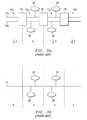
- FIG. 1illustrates a prior art memory cell array
- FIG. 2illustrates a preferred embodiment memory device of the present invention
- FIGS. 3 a and 3 billustrate the reduced line resistance achieved by use of the preferred embodiments of the invention
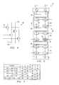
- FIG. 4illustrates a preferred embodiment switch circuit of the present invention
- FIG. 5is a truth table illustrating the operation of the switch circuits
- FIG. 6is a portion of a preferred embodiment of the present invention.
- FIG. 7is another preferred embodiment memory device of the present invention.
- FIG. 1illustrates a prior art MRAM array 10 .
- the MRAM array 10comprises bit lines 12 and word lines 14 which intersect to form points 16 .
- At each point 16is located a memory cell 18 .
- the bit lines 12 and word lines 14each have a decoder (not shown) which contains circuitry to provide a programming current I to the bit line 12 and word line 14 .
- the bit and word lines 12 , 14can be shortened to reduce the resistance. Short bit and word lines, however, result in small arrays that increase the physical space needed. With decreasing physical size of semiconductor devices, this proposes an unacceptable condition.
- the short bit and word lines 12 , 14also result in poor efficiency.
- FIG. 2illustrates a preferred embodiment memory device 20 of the present invention.
- the memory device 20comprises a plurality of bit lines 22 and a plurality of word lines 24 that form a cross-point array with the plurality of bit lines 22 (shown as 22 a and 22 b ).
- a plurality of memory cells 28are located at cross-points 30 which correspond to an intersection of one of the plurality of bit lines 22 with one of the plurality of word lines 24 .
- Coupled to the plurality of bit lines 22is a bit decoder 32 having current sources 34 and current sinks 36 .
- a word decoder 38is coupled to the plurality or word lines 24 .
- the word decoder 38also has current sources 34 and current sinks 36 .
- a first series of switch circuits 40is coupled to two adjacent bit lines 22 .
- the first series of switch circuits 40is located along two adjacent bit lines 22 resulting in the array 26 being divided into segments 42 along the adjacent bit lines.
- the two adjacent bit lines 22are divided into three segments, however, it should be appreciated by those skilled in the art that any number of switch circuits can be used along two adjacent bit lines 22 to divide the array 26 into any number of segments 42 .
- the number of switches usedis determined by the resistance and available space beneath the array.
- Each of the segments 42will contain multiple memory cells 28 , preferably in the range of 128 to 256 memory cells 28 . In FIG. 2, each of the segments 42 is shown having only two memory cells 28 for clarity.
- a programming current Iwould be delivered to the corresponding bit line 22 of a given memory cell 28 to be selected for writing.
- the programming current I pis divided between two adjacent bit lines 22 a, 22 b. About one-half of the programming current I p is provided to each of the two adjacent bit lines 22 a, 22 b.
- any portion of the programming current I pcan be provided to each of two adjacent bit lines 22 a, 22 b as is sufficient to allow the array to operate as described.
- the switch circuits 40are utilized to provide the entire programming current I p to one of the bit lines 22 a or 22 b in a segment 42 .
- the overall resistanceis lowered without shortening the bit lines 22 a, 22 b. This is because the programming current flows through two conductors 22 a and 22 b in two of the segments and only flows through a single conductor for the one segment containing the memory cell to be programmed.
- FIGS. 3 a and 3 billustrate the reduced line resistance achieved by the use of the preferred embodiments of the invention.
- programming current I pflows through both lines 22 a and 22 b in the first segment 42 a, as well as in segments 42 c and 42 d. Each of these segments, then, have only half the resistance they would otherwise have in a single line implementation of Figure 3 b.
- Segment 42 bwhich contains the memory cell 28 to be programmed, has the full programming current I p flowing through only a single conductor 22 a, so that the memory cell connected to conductor 22 a receives the full programming current I p,
- This segment 42 bwould contribute the same amount of line resistance as a prior art bit line, because the current is flowing though only one conductor.
- the line resistance for line 14 of FIG. 3 bis 4*R (normalized to the resistance of one line segment of line 14 .
- the cumulative line resistance for the embodimentis shown in FIG. 3 a is 2.5*R.
- the illustrated embodimentprovides only 5 ⁇ 8 the total line resistance or a reduction of 37.5% of line resistance over the prior art.
- additional line resistance improvementcan be obtained as the number of switch circuits, and hence line segments, increases.
- the above described modelis not entirely accurate, however, as the on state resistance of switch circuit 40 must also be taken into account. Using well known CMOS technology, however, the on state resistance of the switch circuit can be minimized, as discussed further below.
- FIG. 4illustrates a preferred embodiment switch circuit 40 of the present invention that allows a memory cell array to be divided into segments.
- the segmentseffectively shorten the length of bit and word lines that are activated by the current I p at any given time. This “shortened” line length within a segment reduces the resistance across the bit lines, providing improved operation of the memory device.
- the preferred embodiment switch circuit 40comprises transistors T 1 , T 2 , T 3 , and T 4 .
- the transistors T 1 , T 2 , T 3 , and T 4are turned on by control lines 54 which are typically connected to a control circuit (not shown).
- the control circuitis realized with decoders 32 and 34 .
- switch circuit 40illustrates how turning on the various combinations of transistors T 1 , T 2 , T 3 , and T 4 provides the entire current I p through one or the other of two adjacent bit lines 56 and 58 or the current originally provided to each of the two adjacent bit lines 56 , 58 is continued through each of the two adjacent bit lines 56 , 58 . In the latter state, neither of the two adjacent bit lines 56 , 58 in a segment is selected.
- switch circuit 40is discussed in greater detail below with reference to the figures.
- the switch circuits along the two adjacent bit lines 56 , 58can be activated by their respective control signals to provide programming current to either of the bit lines 56 , 58 in a particular segment.
- three switch circuits 60 , 62 , 64are illustrated.
- the three switch circuits 60 , 62 , 64divide the array into three segments 66 , 68 , 70 thus shortening the length of the bit lines 56 , 58 that can be provided programming current at any given time.
- About one-half of the programming current I pis originally provided to each of the bit lines 56 and 58 .
- the switch circuit 60will operate to turn on transistors T 1 and T 2 (see truth table in FIG. 5 and the schematic of FIG. 4) to continue to allow about one-half of the programming current I p to flow to each of the bit lines 56 , 58 . In this state, none of the memory cells coupled to the portions of bit lines 56 , 58 residing in segment 66 will be selected. Because the memory cell 72 resides in segment 68 , the next switch circuit 62 must be programmed to provide programming current I p to bit line 58 . Referring to the truth table in FIG. 5 and the schematic of FIG. 4, to provide the entire programming current I p to line 58 , transistors T 2 and T 3 must be turned on. Thus, data can be written to the memory cell 72 if its corresponding word line 78 is also provided with programming current I p .
- the programming current I pshould flow through both conductors 56 and 58 .
- the succeeding switch circuit 64must be programmed to allow the programming current I p to be split between those portions of the bit lines 56 , 58 that reside in segment 70 .
- transistors T 2 and T 4must be turned on. This is accomplished by splitting the programming current I p coming from that portion of bit line 58 that resides in segment 68 .
- the control circuit(not shown) must be designed to program the control lines to each of the switch circuits such that only one memory cell in a corresponding segment and at a corresponding bit line can receive the programming current at any given time.
- switch circuitscan be utilized on the word lines instead of the bit lines to reduce the amount of resistance across the word lines.
- switch circuits 80are utilized on both the bit and word lines 82 and 84 , respectively, as shown in FIG. 7 to reduce the amount of resistance across both the bit and word lines 83 , 84 .
- the switch circuit logicis located beneath the array to reduce the amount of physical space needed across the array. Because the array in the MRAM is free of transistors, there is an opportunity to put some logic beneath the array.
Landscapes
- Engineering & Computer Science (AREA)
- Microelectronics & Electronic Packaging (AREA)
- Computer Hardware Design (AREA)
- Semiconductor Memories (AREA)
- Mram Or Spin Memory Techniques (AREA)
- Hall/Mr Elements (AREA)
- Read Only Memory (AREA)
Abstract
Description
- This patent claims the benefit of U.S. Provisional Patent Application No. 60/263,984, filed Jan. 24, 2001, which is incorporated herein by reference.[0001]
- This invention relates to semiconductor memory devices and more particularly to a random access memory architecture having lowered bit and word line resistance across the architecture.[0002]
- Traditional memory devices, such as DRAM and FLASH memory devices, generally include an array of word and bit lines that intersect to form an array. At each intersection is coupled a memory cell. Programming current can be provided to the word and bit lines that correspond to the desired memory cell in order to write data to or read data from the memory cell. Magnetic random access memory (MRAM) devices are an emerging technology which provide numerous benefits over DRAM and FLASH memory devices such as non-volatility in contrast to the DRAM device, and faster operation, in contrast to the FLASH memory devices.[0003]
- In traditional memory devices, the length of the word and bit lines that form the array is not typically a design concern. However, the resistance across the bit and word lines is of particular concern in magnetic random access memory (MRAM) devices because the programming current in MRAM devices is higher than in traditional memory devices. The length of the bit and word lines is restricted by the resistance of the lines when the programming current is propagated through the lines. While longer word and bit lines provide larger arrays and better efficiency, the longer word and bit lines have high resistance that results in an excessive voltage drop and undesirable heat generation.[0004]
- In MRAM devices, high resistance across the word and bit lines can cause several problems. One problem is a resulting voltage drop across bit and word lines. If the voltage falls outside of an operating voltage range the memory cell could be damaged.[0005]
- These and other problems are generally solved or circumvented, and technical advantages are generally achieved by the present invention, which in one embodiment provides a random access memory architecture.[0006]
- In one preferred embodiment memory device of the present invention, the device comprises a plurality of bit lines and a plurality of word lines. The plurality of word lines form a cross-point array with the plurality of bit lines. One of a plurality of memory cells is located at each of the cross-points in the array. A bit decoder having a current source and current sink is coupled to the bit lines and a word decoder having a current source and a current sink is coupled to the word lines. A first series of switch circuits are coupled to two adjacent bit lines. The first series of switch circuits are located along the adjacent bit lines resulting in the array being divided into segments along the adjacent bit lines. The memory cell at the corresponding cross-point is selected for writing when the corresponding bit and word lines are provided with a predetermined amount of current.[0007]
- In another preferred embodiment, the switch circuits are located along the word lines. In yet another embodiment, the memory device will utilize a first series of switch circuits along the bit lines and a second series of switch circuits are coupled to two adjacent word lines. The second series of switch circuits are located along the adjacent word lines resulting in the array being divided into segments along the adjacent word lines.[0008]
- One advantage of a preferred embodiment of the present invention is that it reduces the resistance across word and bit lines which limit bit and word line length.[0009]
- Another advantage of a preferred embodiment of the present invention is that it uses an easily implemented switch circuit to reduce resistance across the word and bit lines.[0010]
- A further advantage of a preferred embodiment of the present invention is that some of the architecture of the preferred embodiment can be located beneath the array to reduce the amount of physical space needed.[0011]
- The foregoing has outlined rather broadly the features and technical advantages of the present invention in order that the detailed description of the invention that follows may be better understood. Additional features and advantages of the invention will be described hereinafter, which form the subject of the claims of the invention. It should be appreciated by those skilled in the art that the concepts and specific embodiment disclosed may be readily utilized as a basis for modifying or designing other structures or processes for carrying out the same purposes of the present invention. It should also be realized by those skilled in the art that such equivalent constructions do not depart from the spirit and scope of the invention as set forth in the appended claims.[0012]
- For a more complete understanding of the present invention, and the advantages thereof, reference is now made to the following descriptions taken in conjunction with the accompanying drawing, in which:[0013]
- FIG. 1 illustrates a prior art memory cell array;[0014]
- FIG. 2 illustrates a preferred embodiment memory device of the present invention;[0015]
- FIGS. 3[0016]aand3billustrate the reduced line resistance achieved by use of the preferred embodiments of the invention;
- FIG. 4 illustrates a preferred embodiment switch circuit of the present invention;[0017]
- FIG. 5 is a truth table illustrating the operation of the switch circuits;[0018]
- FIG. 6 is a portion of a preferred embodiment of the present invention; and[0019]
- FIG. 7 is another preferred embodiment memory device of the present invention.[0020]
- The making and using of the presently preferred embodiments is discussed in detail below. It should be appreciated, however, that the present invention provides many applicable inventive concepts that can be embodied in a wide variety of specific contexts. The specific embodiments discussed are merely illustrative of specific ways to make and use the invention, and do not limit the scope of the invention. Although the present invention will be discussed in the context of MRAM applications, it should be appreciated by those skilled in the art that the present invention may be utilized in other applications.[0021]
- FIG. 1 illustrates a prior[0022]
art MRAM array 10. TheMRAM array 10 comprisesbit lines 12 andword lines 14 which intersect to formpoints 16. At eachpoint 16 is located amemory cell 18. Thebit lines 12 andword lines 14 each have a decoder (not shown) which contains circuitry to provide a programming current I to thebit line 12 andword line 14. However, because of the length of thebit line 12 andword line 14, the resistance of these lines when the programming current I is provided is high and causes the voltage to drop across the bit and word lines. The bit andword lines word lines - FIG. 2 illustrates a preferred[0023]
embodiment memory device 20 of the present invention. Thememory device 20 comprises a plurality of bit lines22 and a plurality ofword lines 24 that form a cross-point array with the plurality of bit lines22 (shown as22aand22b). A plurality ofmemory cells 28 are located atcross-points 30 which correspond to an intersection of one of the plurality of bit lines22 with one of the plurality ofword lines 24. Coupled to the plurality of bit lines22 is abit decoder 32 havingcurrent sources 34 andcurrent sinks 36. Aword decoder 38 is coupled to the plurality orword lines 24. Theword decoder 38 also hascurrent sources 34 andcurrent sinks 36. A first series ofswitch circuits 40 is coupled to two adjacent bit lines22. The first series ofswitch circuits 40 is located along two adjacent bit lines22 resulting in thearray 26 being divided intosegments 42 along the adjacent bit lines. For exemplary purposes the two adjacent bit lines22 are divided into three segments, however, it should be appreciated by those skilled in the art that any number of switch circuits can be used along two adjacent bit lines22 to divide thearray 26 into any number ofsegments 42. The number of switches used is determined by the resistance and available space beneath the array. Each of thesegments 42 will containmultiple memory cells 28, preferably in the range of 128 to 256memory cells 28. In FIG. 2, each of thesegments 42 is shown having only twomemory cells 28 for clarity. - Referring back to FIG. 1, in the prior art, a programming current I would be delivered to the corresponding bit line[0024]22 of a given
memory cell 28 to be selected for writing. In the present invention the programming current Ipis divided between twoadjacent bit lines adjacent bit lines adjacent bit lines memory cell 28, theswitch circuits 40 are utilized to provide the entire programming current Ipto one of the bit lines22aor22bin asegment 42. By providing programming current Ipto only thatsegment 42, the overall resistance is lowered without shortening the bit lines22a,22b.This is because the programming current flows through twoconductors - FIGS. 3[0025]aand3billustrate the reduced line resistance achieved by the use of the preferred embodiments of the invention. As illustrated, programming current Ipflows through both
lines first segment 42a,as well as insegments Segment 42b,which contains thememory cell 28 to be programmed, has the full programming current Ipflowing through only asingle conductor 22a,so that the memory cell connected toconductor 22areceives the full programming current Ip,Thissegment 42bwould contribute the same amount of line resistance as a prior art bit line, because the current is flowing though only one conductor. Cumulatively, the line resistance forline 14 of FIG. 3bis 4*R (normalized to the resistance of one line segment ofline 14. By contrast, the cumulative line resistance for the embodiment is shown in FIG. 3ais 2.5*R. As such, the illustrated embodiment provides only ⅝ the total line resistance or a reduction of 37.5% of line resistance over the prior art. One skilled in the art will recognize that additional line resistance improvement can be obtained as the number of switch circuits, and hence line segments, increases. The above described model is not entirely accurate, however, as the on state resistance ofswitch circuit 40 must also be taken into account. Using well known CMOS technology, however, the on state resistance of the switch circuit can be minimized, as discussed further below. - FIG. 4 illustrates a preferred[0026]
embodiment switch circuit 40 of the present invention that allows a memory cell array to be divided into segments. The segments effectively shorten the length of bit and word lines that are activated by the current Ipat any given time. This “shortened” line length within a segment reduces the resistance across the bit lines, providing improved operation of the memory device. - The preferred[0027]
embodiment switch circuit 40 comprises transistors T1, T2, T3, and T4. The transistors T1, T2, T3, and T4 are turned on bycontrol lines 54 which are typically connected to a control circuit (not shown). In the preferred embodiments, the control circuit is realized withdecoders switch circuit 40, the path of the programming current Ipcan be changed to select particular segments in the memory device. The truth table of FIG. 5, for example, illustrates how turning on the various combinations of transistors T1, T2, T3, and T4 provides the entire current Ipthrough one or the other of twoadjacent bit lines adjacent bit lines adjacent bit lines adjacent bit lines switch circuit 40 is discussed in greater detail below with reference to the figures. - Referring to FIG. 6 which shows a portion of the[0028]
array 26 within thememory device 20, the switch circuits along the twoadjacent bit lines switch circuits switch circuits segments memory cell 72 is to be selected for writing, the entire programming current Ipwill be provided to that portion ofbit line 58 that resides insegment 68. To accomplish this, theswitch circuit 60 will operate to turn on transistors T1 and T2 (see truth table in FIG. 5 and the schematic of FIG. 4) to continue to allow about one-half of the programming current Ipto flow to each of the bit lines56,58. In this state, none of the memory cells coupled to the portions ofbit lines segment 66 will be selected. Because thememory cell 72 resides insegment 68, thenext switch circuit 62 must be programmed to provide programming current Ipto bitline 58. Referring to the truth table in FIG. 5 and the schematic of FIG. 4, to provide the entire programming current Ipto line58, transistors T2 and T3 must be turned on. Thus, data can be written to thememory cell 72 if itscorresponding word line 78 is also provided with programming current Ip. - In order to lesson the line resistance of the[0029]
next segment 70, the programming current Ipshould flow through bothconductors switch circuit 64 must be programmed to allow the programming current Ipto be split between those portions of the bit lines56,58 that reside insegment 70. Again referring to the truth table in FIG. 5, to provide an amount of current less than the programming current to each of theconductors bit line 58 that resides insegment 68. Thus, the control circuit (not shown) must be designed to program the control lines to each of the switch circuits such that only one memory cell in a corresponding segment and at a corresponding bit line can receive the programming current at any given time. - In another embodiment of the present invention, switch circuits can be utilized on the word lines instead of the bit lines to reduce the amount of resistance across the word lines. In yet another[0030]
embodiment switch circuits 80 are utilized on both the bit andword lines word lines 83,84. In another embodiment the switch circuit logic is located beneath the array to reduce the amount of physical space needed across the array. Because the array in the MRAM is free of transistors, there is an opportunity to put some logic beneath the array. - Although the present invention and its advantages have been described in detail, it should be understood that various changes, substitutions and alterations can be made herein without departing from the spirit and scope of the invention as defined by the appended claims. Moreover, the scope of the present application is not intended to be limited to the particular embodiments of the process, machine, manufacture, composition of matter, means, methods and steps described in the specification. As one of ordinary skill in the art will readily appreciate from the disclosure of the present invention, processes, machines, manufacture, compositions of matter, means, methods, or steps, presently existing or later to be developed, that perform substantially the same function or achieve substantially the same result as the corresponding embodiments described herein may be utilized according to the present invention. Accordingly, the appended claims are intended to include within their scope such processes, machines, manufacture, compositions of matter, means, methods, or steps.[0031]
Claims (20)
Priority Applications (8)
| Application Number | Priority Date | Filing Date | Title |
|---|---|---|---|
| US09/965,086US6584006B2 (en) | 2001-01-24 | 2001-09-27 | MRAM bit line word line architecture |
| DE60226986TDE60226986D1 (en) | 2001-01-24 | 2002-01-24 | MRAM BITLEITUNGWORTLEITUNGSARCHITEKTUR |
| CNB028040732ACN100338683C (en) | 2001-01-24 | 2002-01-24 | MRAM bit line word line architecture |
| JP2002560138AJP3996061B2 (en) | 2001-01-24 | 2002-01-24 | Memory device and memory cell selection method |
| PCT/US2002/001925WO2002059899A2 (en) | 2001-01-24 | 2002-01-24 | Mram bit line word line architecture |
| TW091101141ATW546650B (en) | 2001-01-24 | 2002-01-24 | MRAM bit line word line architecture |
| KR1020037009811AKR100565109B1 (en) | 2001-01-24 | 2002-01-24 | MRM bit line word line architecture |
| EP02702060AEP1435098B1 (en) | 2001-01-24 | 2002-01-24 | Mram bit line word line architecture |
Applications Claiming Priority (2)
| Application Number | Priority Date | Filing Date | Title |
|---|---|---|---|
| US26398401P | 2001-01-24 | 2001-01-24 | |
| US09/965,086US6584006B2 (en) | 2001-01-24 | 2001-09-27 | MRAM bit line word line architecture |
Publications (2)
| Publication Number | Publication Date |
|---|---|
| US20020097597A1true US20020097597A1 (en) | 2002-07-25 |
| US6584006B2 US6584006B2 (en) | 2003-06-24 |
Family
ID=26950183
Family Applications (1)
| Application Number | Title | Priority Date | Filing Date |
|---|---|---|---|
| US09/965,086Expired - LifetimeUS6584006B2 (en) | 2001-01-24 | 2001-09-27 | MRAM bit line word line architecture |
Country Status (8)
| Country | Link |
|---|---|
| US (1) | US6584006B2 (en) |
| EP (1) | EP1435098B1 (en) |
| JP (1) | JP3996061B2 (en) |
| KR (1) | KR100565109B1 (en) |
| CN (1) | CN100338683C (en) |
| DE (1) | DE60226986D1 (en) |
| TW (1) | TW546650B (en) |
| WO (1) | WO2002059899A2 (en) |
Cited By (2)
| Publication number | Priority date | Publication date | Assignee | Title |
|---|---|---|---|---|
| US20060158919A1 (en)* | 2004-11-30 | 2006-07-20 | Tsuneo Inaba | Semiconductor memory device |
| EP1662510A3 (en)* | 2004-11-30 | 2006-08-02 | Kabushiki Kaisha Toshiba | Arrangement of write lines in an MRAM device |
Families Citing this family (18)
| Publication number | Priority date | Publication date | Assignee | Title |
|---|---|---|---|---|
| US7233522B2 (en) | 2002-12-31 | 2007-06-19 | Sandisk 3D Llc | NAND memory array incorporating capacitance boosting of channel regions in unselected memory cells and method for operation of same |
| US7505321B2 (en)* | 2002-12-31 | 2009-03-17 | Sandisk 3D Llc | Programmable memory array structure incorporating series-connected transistor strings and methods for fabrication and operation of same |
| US7005350B2 (en)* | 2002-12-31 | 2006-02-28 | Matrix Semiconductor, Inc. | Method for fabricating programmable memory array structures incorporating series-connected transistor strings |
| US6822903B2 (en)* | 2003-03-31 | 2004-11-23 | Matrix Semiconductor, Inc. | Apparatus and method for disturb-free programming of passive element memory cells |
| US7233024B2 (en)* | 2003-03-31 | 2007-06-19 | Sandisk 3D Llc | Three-dimensional memory device incorporating segmented bit line memory array |
| US6879505B2 (en)* | 2003-03-31 | 2005-04-12 | Matrix Semiconductor, Inc. | Word line arrangement having multi-layer word line segments for three-dimensional memory array |
| US7177183B2 (en) | 2003-09-30 | 2007-02-13 | Sandisk 3D Llc | Multiple twin cell non-volatile memory array and logic block structure and method therefor |
| US6972989B2 (en) | 2003-10-10 | 2005-12-06 | Infincon Technologies Ag | Reference current distribution in MRAM devices |
| US6873535B1 (en)* | 2004-02-04 | 2005-03-29 | Taiwan Semiconductor Manufacturing Company, Ltd. | Multiple width and/or thickness write line in MRAM |
| US7359279B2 (en)* | 2005-03-31 | 2008-04-15 | Sandisk 3D Llc | Integrated circuit memory array configuration including decoding compatibility with partial implementation of multiple memory layers |
| US7272052B2 (en)* | 2005-03-31 | 2007-09-18 | Sandisk 3D Llc | Decoding circuit for non-binary groups of memory line drivers |
| US7142471B2 (en)* | 2005-03-31 | 2006-11-28 | Sandisk 3D Llc | Method and apparatus for incorporating block redundancy in a memory array |
| US7054219B1 (en) | 2005-03-31 | 2006-05-30 | Matrix Semiconductor, Inc. | Transistor layout configuration for tight-pitched memory array lines |
| US7471539B2 (en)* | 2005-12-20 | 2008-12-30 | Taiwan Semiconductor Manufacturing Co., Ltd. | High current interconnect structure for IC memory device programming |
| US7480172B2 (en) | 2006-01-25 | 2009-01-20 | Magic Technologies, Inc. | Programming scheme for segmented word line MRAM array |
| US7773405B2 (en) | 2006-06-08 | 2010-08-10 | Nec Corporation | Magnetic random access memory and operating method of magnetic random access memory |
| KR100758299B1 (en)* | 2006-07-25 | 2007-09-12 | 삼성전자주식회사 | Flash memory device and its writing method |
| JP2020155181A (en)* | 2019-03-20 | 2020-09-24 | キオクシア株式会社 | Semiconductor memory device |
Family Cites Families (6)
| Publication number | Priority date | Publication date | Assignee | Title |
|---|---|---|---|---|
| DE3101802A1 (en) | 1981-01-21 | 1982-08-19 | Siemens AG, 1000 Berlin und 8000 München | MONOLITHICALLY INTEGRATED SEMICONDUCTOR MEMORY |
| US5024993A (en)* | 1990-05-02 | 1991-06-18 | Microelectronics & Computer Technology Corporation | Superconducting-semiconducting circuits, devices and systems |
| JPH06318683A (en) | 1993-05-01 | 1994-11-15 | Toshiba Corp | Semiconductor memory device and manufacturing method thereof |
| JP3560266B2 (en) | 1995-08-31 | 2004-09-02 | 株式会社ルネサステクノロジ | Semiconductor device and semiconductor data device |
| DE19853447A1 (en)* | 1998-11-19 | 2000-05-25 | Siemens Ag | Magnetic storage |
| US6111783A (en) | 1999-06-16 | 2000-08-29 | Hewlett-Packard Company | MRAM device including write circuit for supplying word and bit line current having unequal magnitudes |
- 2001
- 2001-09-27USUS09/965,086patent/US6584006B2/ennot_activeExpired - Lifetime
- 2002
- 2002-01-24EPEP02702060Apatent/EP1435098B1/ennot_activeExpired - Lifetime
- 2002-01-24JPJP2002560138Apatent/JP3996061B2/ennot_activeExpired - Fee Related
- 2002-01-24TWTW091101141Apatent/TW546650B/ennot_activeIP Right Cessation
- 2002-01-24CNCNB028040732Apatent/CN100338683C/ennot_activeExpired - Fee Related
- 2002-01-24KRKR1020037009811Apatent/KR100565109B1/ennot_activeExpired - Fee Related
- 2002-01-24WOPCT/US2002/001925patent/WO2002059899A2/enactiveIP Right Grant
- 2002-01-24DEDE60226986Tpatent/DE60226986D1/ennot_activeExpired - Lifetime
Cited By (3)
| Publication number | Priority date | Publication date | Assignee | Title |
|---|---|---|---|---|
| US20060158919A1 (en)* | 2004-11-30 | 2006-07-20 | Tsuneo Inaba | Semiconductor memory device |
| EP1662510A3 (en)* | 2004-11-30 | 2006-08-02 | Kabushiki Kaisha Toshiba | Arrangement of write lines in an MRAM device |
| US7359234B2 (en) | 2004-11-30 | 2008-04-15 | Kabushiki Kaisha Toshiba | Semiconductor memory device |
Also Published As
| Publication number | Publication date |
|---|---|
| CN100338683C (en) | 2007-09-19 |
| KR100565109B1 (en) | 2006-03-30 |
| WO2002059899A2 (en) | 2002-08-01 |
| WO2002059899A3 (en) | 2003-02-13 |
| EP1435098A2 (en) | 2004-07-07 |
| KR20040012715A (en) | 2004-02-11 |
| US6584006B2 (en) | 2003-06-24 |
| TW546650B (en) | 2003-08-11 |
| JP3996061B2 (en) | 2007-10-24 |
| CN1488145A (en) | 2004-04-07 |
| DE60226986D1 (en) | 2008-07-17 |
| JP2004518288A (en) | 2004-06-17 |
| EP1435098B1 (en) | 2008-06-04 |
Similar Documents
| Publication | Publication Date | Title |
|---|---|---|
| US6584006B2 (en) | MRAM bit line word line architecture | |
| US7623369B2 (en) | Method and system for providing a magnetic memory structure utilizing spin transfer | |
| US6496414B2 (en) | Nonvolatile semiconductor memory | |
| KR101365478B1 (en) | A magnetic random access memory circuit | |
| US8284602B2 (en) | Pipe latch circuit of multi-bit prefetch-type semiconductor memory device with improved structure | |
| JP4637388B2 (en) | Thin film magnetic memory device | |
| KR20070122201A (en) | Decoding Circuit for Non-Binary Groups of Memory Line Drivers | |
| US6650567B1 (en) | Nonvolatile semiconductor memories with a NAND logic cell structure | |
| US6947322B2 (en) | Semiconductor memory device | |
| JPWO2010147029A1 (en) | Semiconductor device | |
| KR100748070B1 (en) | Peak program current reduction apparatus and method | |
| JP4646608B2 (en) | Semiconductor memory device | |
| US6606268B2 (en) | Non-volatile semiconductor integrated circuit | |
| JP2010129161A (en) | Semiconductor memory and bit line control method | |
| US6249466B1 (en) | Row redundancy scheme | |
| US7378879B1 (en) | Decoding systems and methods | |
| JP3582773B2 (en) | Semiconductor storage device | |
| US6680857B2 (en) | Unit-architecture with implemented limited bank-column-select repairability | |
| TW202247184A (en) | Memory device | |
| CN119274611A (en) | Memory circuit and method of operating the same | |
| JP2007042192A (en) | Magnetic random access memory |
Legal Events
| Date | Code | Title | Description |
|---|---|---|---|
| AS | Assignment | Owner name:INFINEON TECHNOLOGIES NORTH AMERICA CORP., CALIFOR Free format text:ASSIGNMENT OF ASSIGNORS INTEREST;ASSIGNOR:VIEHMANN, HANS-HEINRICH;REEL/FRAME:012229/0444 Effective date:20010913 | |
| STCF | Information on status: patent grant | Free format text:PATENTED CASE | |
| AS | Assignment | Owner name:INFINEON TECHNOLOGIES AG, GERMANY Free format text:ASSIGNMENT OF ASSIGNORS INTEREST;ASSIGNOR:INFINEON TECHNOLOGIES NORTH AMERICA CORP.;REEL/FRAME:013806/0145 Effective date:20030430 | |
| FEPP | Fee payment procedure | Free format text:PAYOR NUMBER ASSIGNED (ORIGINAL EVENT CODE: ASPN); ENTITY STATUS OF PATENT OWNER: LARGE ENTITY | |
| FPAY | Fee payment | Year of fee payment:4 | |
| AS | Assignment | Owner name:QIMONDA AG,GERMANY Free format text:ASSIGNMENT OF ASSIGNORS INTEREST;ASSIGNOR:INFINEON TECHNOLOGIES AG;REEL/FRAME:023768/0001 Effective date:20060425 Owner name:QIMONDA AG, GERMANY Free format text:ASSIGNMENT OF ASSIGNORS INTEREST;ASSIGNOR:INFINEON TECHNOLOGIES AG;REEL/FRAME:023768/0001 Effective date:20060425 | |
| FPAY | Fee payment | Year of fee payment:8 | |
| FPAY | Fee payment | Year of fee payment:12 | |
| AS | Assignment | Owner name:INFINEON TECHNOLOGIES AG, GERMANY Free format text:ASSIGNMENT OF ASSIGNORS INTEREST;ASSIGNOR:QIMONDA AG;REEL/FRAME:035623/0001 Effective date:20141009 | |
| AS | Assignment | Owner name:POLARIS INNOVATIONS LIMITED, IRELAND Free format text:ASSIGNMENT OF ASSIGNORS INTEREST;ASSIGNOR:INFINEON TECHNOLOGIES AG;REEL/FRAME:036808/0284 Effective date:20150708 |