US20020097486A1 - Optical element change-over control apparatus and microscope using the same - Google Patents
Optical element change-over control apparatus and microscope using the sameDownload PDFInfo
- Publication number
- US20020097486A1 US20020097486A1US09/910,740US91074001AUS2002097486A1US 20020097486 A1US20020097486 A1US 20020097486A1US 91074001 AUS91074001 AUS 91074001AUS 2002097486 A1US2002097486 A1US 2002097486A1
- Authority
- US
- United States
- Prior art keywords
- optical element
- change
- over
- detecting
- origin
- Prior art date
- Legal status (The legal status is an assumption and is not a legal conclusion. Google has not performed a legal analysis and makes no representation as to the accuracy of the status listed.)
- Granted
Links
- 230000003287optical effectEffects0.000titleclaimsabstractdescription168
- 238000000034methodMethods0.000claimsdescription14
- 230000004044responseEffects0.000description6
- 238000005286illuminationMethods0.000description5
- 230000008901benefitEffects0.000description4
- 238000001514detection methodMethods0.000description4
- 230000006870functionEffects0.000description4
- 230000005540biological transmissionEffects0.000description3
- 230000002093peripheral effectEffects0.000description3
- 230000008859changeEffects0.000description2
- 238000010586diagramMethods0.000description2
- 238000012986modificationMethods0.000description2
- 230000004048modificationEffects0.000description2
- 229940000425combination drugDrugs0.000description1
- 239000003814drugSubstances0.000description1
- 229910052736halogenInorganic materials0.000description1
- 150000002367halogensChemical class0.000description1
- 238000003780insertionMethods0.000description1
- 230000037431insertionEffects0.000description1
- QSHDDOUJBYECFT-UHFFFAOYSA-NmercuryChemical compound[Hg]QSHDDOUJBYECFT-UHFFFAOYSA-N0.000description1
Images


Classifications
- G—PHYSICS
- G02—OPTICS
- G02B—OPTICAL ELEMENTS, SYSTEMS OR APPARATUS
- G02B21/00—Microscopes
- G02B21/24—Base structure
- G02B21/248—Base structure objective (or ocular) turrets
Definitions
- the present inventionrelates to an optical element change-over control apparatus for automatically changing necessary optical elements for various observations and an optical microscope using the control apparatus.
- the objective lenscan be designed for 6-stage change-over, and the viewing method for 4-stage change-over.
- the degree of freedom of microscope controlchanges, so that the control function must be changed in many cases.
- the degree of freedom of the currently set unite.g., the number of holes of the revolver, should be learned in advance by any method.
- Jpn. Pat. Appln. KOKAI Publication No. 8-179218for example, is a microscopic system, which comprises motor-operated loading-unloading means for inserting into and removing various optical members from an optical path, detecting means for detecting any of the optical members in the optical path, input means for inputting control instructions from an operator, and control means.
- the control meansreceives information on the state of the optical member from the detecting means, and delivers a control command to the loading-unloading means to control the insertion of the optical member concerned in response to a control instruction inputted through the input means.
- the microscopic systemfurther comprises setting means for optionally setting element data on various optical members, memory means capable of storing the element data on the optical members set by means of the setting means and holding the element data even in a power-off state, and display means for displaying the contents of the element data on the optical members.
- optical members having new element datacan be added to the optical member unit, and optimum control of a lighting system and an aiming system can be carried out with use of the added optical members.
- the environment of the microscopecan be easily built up, and the resulting microscopic system can enjoy improved operating efficiency.
- the general control of the microscopeis optimized in accordance with only element data on the objective lens that is attached to the revolver and element data on a filter that is attached to the cube cassette and applied to the viewing method.
- the controlcannot cope with change of the number of change-over stages of the optical member unit, such as the number of holes of the revolver and the number of change-over stags of the cube cassette.
- the present inventionhas been contrived in consideration of these circumstances, and its object is to provide an optical element change-over control apparatus, capable of carrying out smooth microscopic operation by detecting the number of change-over stages of optical element change-over units, such as a revolver, cube cassette, filter turret, etc., without changing the control function even in the case where the number of change-over stages of the change-over units is changed as the change-over units attached to the body of a microscope are replaced, and a microscope using the same.
- optical element change-over control apparatuscapable of carrying out smooth microscopic operation by detecting the number of change-over stages of optical element change-over units, such as a revolver, cube cassette, filter turret, etc.
- an optical element change-over control apparatuscomprises: an optical element change-over member capable of holding a plurality of optical elements and rotating alternatively to locate a specific optical element on an optical path; a driving element for rotating the optical element change-over member; a positioning detecting element for detecting the selected optical element being positioned so that the optical element stays in a predetermined position on the optical path and outputting positioning signals; an origin detecting element for detecting the point of origin of the optical element change-over member; and a control element for driving the driving element to rotate the optical element change-over member and counting the positioning signals delivered from the positioning detecting element during the time interval that elapses from the instant that the point of origin of the optical element change-over member is first detected by means of the origin detecting element until the point of origin of the optical element change-over member is secondly detected by means of the origin detecting element, thereby detecting the number of change-over stages of the optical element change-over member.
- a microscopic apparatususes an optical element change-over control apparatus, which comprises: an optical element change-over member capable of holding a plurality of optical elements and rotating alternatively to locate a specific optical element on an optical path; a driving element for rotating the optical element change-over member; a positioning detecting element for detecting the selected optical element being positioned so that the optical element stays in a predetermined position on the optical path and outputting positioning signals; an origin detecting element for detecting the point of origin of the optical element change-over member; and a control element for driving the driving element to rotate the optical element change-over member and counting the positioning signals delivered from the positioning detecting element during the time interval that elapses from the instant that the point of origin of the optical element change-over member is first detected by means of the origin detecting element until the point of origin of the optical element change-over member is secondly detected by means of the origin detecting element, thereby detecting the number of change-over stages of the optical element change-over member.
- a method for detecting the number of change-over stages of an optical element change-over membercapable of holding a plurality of optical elements and rotating alternatively to locate a specific optical element on an optical path, the method comprising: a member rotating step of driving a driving element to rotate the optical element change-over member; a first origin position detecting step of detecting the origin position of the optical element change-over member by means of an origin detecting element; a positioning signal detecting step of determining whether or not a positioning signal, indicative of the selected optical element being positioned so that the optical element stays in a predetermined position on the optical path, is detected after the origin position is detected and incrementing a count value indicative of the number of change-over stages of the optical element change-over member by one every time the positioning signal is detected; and a second origin position detecting step of determining whether or not the origin position of the optical element change-over member is detected again during the execution of the positioning signal detecting step and stopping the rotation of the optical element change
- FIG. 2is a diagram showing a control section and an operating section of the apparatus according to the first embodiment
- FIG. 3is a front view of a filter cassette of the apparatus according to the first embodiment
- FIG. 4is a partial side view of the filter cassette of the apparatus according to the first embodiment
- FIG. 7is a flowchart for controlling the apparatus according to the first embodiment.
- FIG. 8is a flowchart for controlling an apparatus according to a second embodiment of the invention.
- FIGS. 1 and 2A first embodiment of the present invention will now be described with reference to FIGS. 1 and 2.
- a light source 1 for transmissive illuminatione.g., a halogen lamp
- the filter turret 4is fitted with six different filters for six-stage change-over.
- These filersinclude, for example, an ND filter 4 a for adjusting the brightness of the light source 1 for transmission without changing its color temperature, a compensating filter 4 b for color correction. Desired filters can be alternatively inserted into and removed from the lighting optical system.
- Illumination light transmitted through the filter turret 4 for transmissionis guided through a transmissive aperture stop 5 , condenser optical element unit 6 , and condenser top lens unit 7 and applied to a specimen S on a specimen stage 8 from under the stage 8 .
- the condenser optical element unit 6is composed of six different condensers 6 a to 6 f (of which 6 c to 6 f are not shown) that can be alternatively inserted into and removed from the optical path.
- the condenser top lens unit 7is composed of a plurality of condenser top lenses 7 a and 7 b that can be alternatively inserted into the optical path.
- the specimen stage 8can two-dimensionally move the specimen S within a plane that extends at right angles to the optical axis of the microscope and vertically move for focusing along the optical axis.
- a six-stage revolver 10that can be loaded with six different objective lenses 9 a to 9 f (of which 9 b to 9 f are not shown) is removably held for rotation on the lower surface of an arm end portion (not shown) of the microscope. Any of the objective lenses 9 a to 9 f can be inserted into or removed from the optical path on the optical axis in the observational light path by rotating the revolver 10 . Further, a cube cassette 11 is located on the optical axis on the observational light path on the upper surface of the arm end portion of the microscope.
- the cube cassette 11is in the form of a four-stage turret that is loaded with four different filter cubes 11 a to 11 d (of which 11 c and 11 d are not shown). Any of the filter cubes can be alternatively inserted into and removed from the optical path by various microscopic methods.
- a light source 14 for incident illuminationformed of a mercury vapor lamp
- a collector lens 15is condensed by means of a collector lens 15 , and landed on an incident light filter turret 16 that is changeably attached to the microscope body (not shown).
- the filter turret 16which is changeable in six stages, is fitted with six different filters 16 a to 16 f (of which 16 c to 16 f are not shown).
- the filter 16 ais an ND filter for adjusting the brightness of the light source 14 for incident illumination without changing its color temperature, while the filter 16 b is a compensating filter for color correction. Any of the filters 16 a to 16 f can be alternatively inserted into and removed from the optical path.
- a control section 19 and an operating section 20 shown in FIG. 1will now be described with reference to FIG. 2.
- the control section 19is composed of a CPU 21 , ROM 22 , RAM 23 , and nonvolatile memory 24 , which are connected to one another by means of their respective CPU buses.
- the ROM 22is stored with programs in which control contents are described, while the RAM 23 is loaded with data for control operation.
- the nonvolatile memory 24which may be an EEPROMM, NVRAM, or flash memory, stores or reads necessary information as the programs are executed.
- the operating section 20is formed of a display element 25 and a switch input element 26 , which are connected to the CPU 21 .
- the operating section 20delivers an operation signal from the switch input element 26 to the CPU 21 , and controls position information on various driving elements 27 to 31 (mentioned later).
- control section 19is provided with an external I/F (not shown) such as an RS-232C, USB, or Ethernet.
- an external controllersuch as a PC
- the control section 19can carry out driving element control that is equivalent to operation through the operating section 20 .
- the transmissive filter turret driving element 27rotates the transmissive filter turret 4 , thereby alternatively inserting into or removing one of filters 4 a to 4 f from the optical path.
- a condenser unit driving element 28In response to a driving signal from the control section 19 , a condenser unit driving element 28 carries out stop adjustment for the transmissive aperture stop 5 , and rotates the condenser optical element unit 6 and the condenser top lens unit 7 , thereby alternatively inserting into or removing the desired optical element 6 a or 6 b and the top lens 7 a or 7 b from the optical path.
- a revolver driving element 29rotates the revolver 10 , thereby alternatively inserting into or removing one of the objective lenses 9 a to 9 f from the optical path.
- a cube cassette driving element 30rotates the cube cassette 11 , thereby alternatively inserting into or removing one of the filter cubes 11 a to 11 d from the optical path.
- an incident filter turret driving element 31rotates the incident filter turret 16 , thereby alternatively inserting into or removing one of the filters 16 a to 16 f from the optical path.
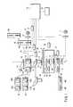
- FIGS. 3 and 4are a front view and a side view, respectively, of the cube cassette 11 .
- the cubes 11 a to 11 dare arranged at equal spaces on the circumference of a circle on a disc 11 - 1 .
- the disc 11 - 1is rotated by means of a pulse motor 30 - 1 of the cube cassette driving element 30 .
- a magnet 11 - 2 for detecting the origin position of the disc 11 - 1is attached to the outer peripheral surface of the disc 11 - 1 .
- a Hall element 30 - 2 of the cube cassette driving element 30is located in a position opposite to the magnet 11 - 2 .
- openings 11 - 3 to 11 - 6are provided on the outer periphery of the disc 11 - 1 .
- the openings 11 - 3 to 11 - 6are used to detect positioning of the cubes 11 a to 11 d on an optical path OP.
- held on the cube cassette driving element 30is a photo-interrupter 30 - 3 , which detects the openings 11 - 3 to 11 - 6 .
- the filter cube 11 cis located on the optical path OP, correct positioning of the cube 11 c on the optical path OP can be detected by detecting the presence of the opening 11 - 5 by means of the photo-interrupter 30 - 3 .
- the filter turret 4 , revolver 10 , and incident filter turret 16are provided with a magnet for origin position detection and openings for positioning detection each.
- the transmissive filter turret driving element 27 , condenser unit driving element 28 , and revolver driving element 29are provided with a Hall element and a photo-interrupter each.
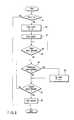
- the control section 19is started to clear the count number in a counter (not shown) (C: 0 ; Step S 1 ). Thereafter, the disc 11 - 1 is rotated by means of the cube cassette driving element 30 (Step S 2 ). As the disc 11 - 1 rotates in this manner, the position of the magnet 11 - 2 on the disc 11 - 1 is detected by means of the Hall element 30 - 2 . If the origin position of the disc 11 - 1 is detected by doing this (Step S 3 ), counting detected positioning signals is started (Step S 4 ). As the disc 11 - 1 further rotates so that the opening 11 - 5 is detected by means of the photo-interrupter 30 - 3 , the positioning signals are detected, and the count C is upped (C: 1 ; Step S 5 ).
- counting the positioning signals for the disc 11 - 1is continued. As the disc 11 - 1 then rotates, the opening 11 - 4 reaches the photo-interrupter 30 - 3 , whereupon the count C is upped (C: 2 ; Step S 5 ). Likewise, the detected positioning signals for the openings 11 - 3 and 11 - 6 continue to be counted in succession, and the count C is upped (C: 3 , C: 4 ; Step S 5 ) on each occasion.
- the magnet 11 - 2 that is held on the disc 11 - 1is detected again by means of the Hall element 30 - 2 that is held in the cube cassette driving element 30 , and therefore, the origin position of the disc 11 - 1 is detected again (Step S 6 ), whereupon the rotation of the disc 11 - 1 stops (Step S 7 ). Then, the count (C: 4 ) is loaded into the nonvolatile memory 24 , whereupon the searching operation is finished. The number of change-over stages (four stages) of the cube cassette 11 can be detected by examining the value of the count C.
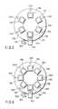
- FIG. 5shows a six-stage cube cassette 110 that is used in place of the cube cassette 11 . Searching operation with use of the cube cassette 110 will now be described with reference to the flowchart of FIG. 7.
- a magnet 110 - 2 for origin detectionis attached to the peripheral edge of the disc 110 - 1 , six different cubes 110 a to 10 f are placed on the disc 110 - 1 , and openings 110 - 3 to 110 - 8 are provided corresponding to the cubes 110 a to 110 f , respectively.
- the control section 19starts the searching operation for the cube cassette 110 .
- the count number in the counter(not shown) is cleared (C: 0 ; Step S 1 ).
- the disc 110 - 1is rotated by means of the cube cassette driving element 30 (Step S 2 ).
- the position of the magnet 110 - 2 on the disc 110 - 1is detected by means of the Hall element 30 - 2 . If the origin position of the disc 110 - 1 is detected by doing this (Step S 3 ), the counter starts counting detected positioning signals (Step S 4 ).
- the positioning signalsare detected, and the count C is upped (C: 1 ; Step S 5 ). Further, counting the positioning signals for the disc 110 - 1 is continued. If the opening 110 - 5 is detected by means of the photo-interrupter 30 - 3 as the disc 110 - 1 rotates, the count C is upped (C: 2 ; Step S 5 ). Likewise, the opening 110 - 4 is detected, and the count C is upped (C: 3 ; Step S 5 ). Likewise, the openings 110 - 3 , 110 - 8 and 110 - 7 are detected, and the count C is upped (C: 4 , C: 5 , C: 6 ; Step S 5 ).
- the rotation of the disc 110 - 1is continued, moreover, the magnet 110 - 2 held on the disc 110 - 1 is detected again by means of the Hall element 30 - 2 that is held in the cube cassette driving element 30 . Thereupon, the origin position of the disc 110 - 1 is detected (Step S 6 ), and the rotation of the disc 110 - 1 stops (Step S 7 ). Then, the count (C: 6 ) is loaded into the nonvolatile memory 24 , whereupon the searching operation is finished. The number of change-over stages (six stages) of the cube cassette 11 can be detected by examining the value of the count C.
- FIG. 6shows an eight-stage cube cassette 120 .
- the number of change-over stages (eight stages) of the cube cassette 120can be also detected with reference to the flowchart of FIG. 7.
- a magnet 120 - 2 for origin detectionis attached to the peripheral edge of a disc 120 - 1 , eight different cubes 120 a to 120 h are placed on the disc 120 - 1 , and openings 120 - 3 to 120 - 10 are provided corresponding to the cubes 120 a to 120 f, respectively.
- the controlcan be started when the apparatus is switched on as the so-called initializing operation. If searching operation is started by a first cycle of change-over operation for the cube cassette based on the operation of the operating section 20 , instead of switching the apparatus on, the searching operation can be carried out only when necessary. Thus, the time that is required by the searching operation with the power on can be saved.
- the cube cassettes 11 , 110 and 120have been described as components that constitute an optical element change-over control apparatus.
- searching operation for the number of change-over stages of the optical elementcan be also carried out with respect to replaceable transmissive filter turrets 4 and 40 , revolvers 10 and 100 , and incident filter turrets 16 and 160 shown in FIG. 1.
- switches 100 a and 100 bare additionally used as setting members for previously setting the control section 19 or the operating section 20 to settle whether or not to execute operation for detecting the point of origin of the optical element change-over member.
- dip switchesare used as the switches 100 i a l and 100 b.
- Step S 1the state of the switch 100 a or 100 b that is attached to the control section 19 or the operating section 20 is examined (Step S 1 ). If the switch 100 a or 100 b is off, searching operation is not executed. In this case, the value of the count C is read from the nonvolatile memory 24 and detected as the number of change-over stages of the cube cassette (END). If the switch 100 a or 100 b is on, on the other hand, searching operation for the cube cassette 11 is started. After the control section 19 is started to clear the count number in the counter (not shown) (C: 0 ; Step S 2 ), the disc 11 - 1 is rotated by means of the cube cassette driving element 30 (Step S 3 ).
- Step S 4the position of the magnet 11 - 2 on the disc 11 - 1 is detected by means of the Hall element 30 - 2 . If the origin position of the disc 11 - 1 is detected by doing this (Step S 4 ), counting the positioning signals is started (Step S 5 ). As the disc 11 - 1 further rotates so that the opening 11 - 5 is detected by means of the photo-interrupter 30 - 3 , the positioning signals are outputted, and the count C is upped (C: 1 ; Step S 6 ). Further, counting the positioning signals for the disc 11 - 1 is continued.
- the count Cis upped (C: 2 ; Step S 6 ).
- the positioning signals for the openings 11 - 3 and 11 - 6continue to be counted in succession, and the count C is upped (C: 3 , C: 4 ; Step S 6 ) on each occasion.
- the magnet 11 - 2 that is held on the disc 11 - 1is detected again by means of the Hall element 30 - 2 that is held in the cube cassette driving element 30 , and therefore, the origin position of the disc 11 - 1 is detected (Step S 7 ), whereupon the rotation of the disc 11 - 1 stops (Step S 8 ). Then, the value of the count C (C: 4 ) is loaded into the nonvolatile memory 24 , whereupon the searching operation is finished (END).
- the number of change-over stages (four stages) of the cube cassette 11can be obtained by examining the value of the count C.
- Step S 1the state of the switch 100 a or 100 b that is attached to the control section 19 or the operating section 20 is examined. If the switch 100 a or 100 b is off, searching operation is not executed. In this case, the count is read from the nonvolatile memory 24 , and its value is detected as the number of change-over stages of the cube cassette (END). If the switch 100 a or 100 b is on, on the other hand, searching operation for the cube cassette 110 is started. After the count number in the counter (not shown) is first cleared (C: 0 ; Step S 2 ), the disc 110 - 1 is rotated by means of the cube cassette driving element 30 (Step S 3 ).
- Step S 4the counter starts counting the positioning signals.
- the disc 110 - 1is further rotated so that the opening 110 - 6 is detected by means of the photo-interrupter 30 - 3 , the positioning signals are outputted, and the count C is upped (C: 1 ; Step S 5 ). Further, counting the positioning signals for the disc 110 - 1 is continued.
- the count Cis upped (C: 2 ; Step S 5 ).
- the count Cis upped (C: 3 ; Step S 5 ) as the opening 110 - 4 is detected by means of the photo-interrupter 30 - 3 .
- the count Cis upped (C: 4 , C: 5 , C: 6 ; Step S 6 ) as the openings 110 - 3 , 110 - 8 and 110 - 7 are detected in succession by means of the photo-interrupter 30 - 3 .
- the magnet 110 - 2 that is held on the disc 110 - 1is detected again by means of the Hall element 30 - 2 that is held in the cube cassette driving element 30 , and therefore, the origin position of the disc 110 - 1 is detected (Step S 7 ), whereupon the rotation of the disc 110 - 1 stops (Step S 8 ). Then, the value of the count C (C: 6 ) is loaded into the nonvolatile memory 24 , whereupon the searching operation is finished.
- the number of change-over stages (six stages) of the cube cassette 110can be detected by examining the value of the count C.
- the number of change-over stages (eight stages) of the cube cassette 120can be also detected with reference to the flowchart of FIG. 8.
- the control according to second embodiment described abovecan be started when the apparatus is switched on as the so-called initializing operation. If searching operation is started by a first cycle of change-over operation for the cube cassette based on the operation of the operating section 20 , instead of switching the apparatus on, the searching operation can be carried out only when necessary. Thus, the time that is required by the searching operation with the power on can be saved.
- the cube cassettes 11 , 110 and 120have been described as components that constitute the optical element change-over control apparatus.
- the number of change-over stagescan be also detected by means of the change-over control apparatus with respect to the transmissive filter turrets 4 and 40 , revolvers 10 and 100 , and incident filter turrets 16 and 160 shown in FIG. 1.
- the optical element unit to be attached to the microscope bodycan be replaced. If the number of change-over stages is changed, therefore, the control function need not be changed at all. Thus, the microscope can be smoothly operated by detecting the number of change-over stages of the newly set optical element unit.
Landscapes
- Physics & Mathematics (AREA)
- Chemical & Material Sciences (AREA)
- Analytical Chemistry (AREA)
- General Physics & Mathematics (AREA)
- Optics & Photonics (AREA)
- Microscoopes, Condenser (AREA)
- Lens Barrels (AREA)
- Lenses (AREA)
Abstract
Description
- This application is based upon and claims the benefit of priority from the prior Japanese Patent Application No. 2000-224345, filed Jul. 25, 2000, the entire contents of which are incorporated herein by reference.[0001]
- The present invention relates to an optical element change-over control apparatus for automatically changing necessary optical elements for various observations and an optical microscope using the control apparatus.[0002]
- Various microscopic observation methods are used in the fields of medicine, biology, industries, etc. These observation methods, including the bright-field, dark-field, differential-interference contrast, and fluorescent observation methods, are changed over to one another by selecting necessary optical elements.[0003]
- Further, a plurality of objective lens are used, and two or more types of objective lenses are required depending on the technical fields and applications. In order to meet this requirement with high efficiency, optical element change-over means, such as a revolver, cube cassette, filter turret, etc., are developed as component units that can be attached to a microscope. So-called system microscopes are prevailing microscopes that incorporate components selected according to the field of application and have the necessary number of change-over stages for the viewing method. One such system microscope may use, for example, a six-hole revolver, among other ones including 5-, 7-, and 8-hole revolvers. The cube cassette may, for example, be a 4-hole cube cassette selected among other ones including 6- and 8-hole cube cassettes. With this arrangement, the objective lens can be designed for 6-stage change-over, and the viewing method for 4-stage change-over. If the unit is replaced in the microscope of this type, the degree of freedom of microscope control changes, so that the control function must be changed in many cases. Further, the degree of freedom of the currently set unit, e.g., the number of holes of the revolver, should be learned in advance by any method. Described in Jpn. Pat. Appln. KOKAI Publication No. 8-179218, for example, is a microscopic system, which comprises motor-operated loading-unloading means for inserting into and removing various optical members from an optical path, detecting means for detecting any of the optical members in the optical path, input means for inputting control instructions from an operator, and control means. The control means receives information on the state of the optical member from the detecting means, and delivers a control command to the loading-unloading means to control the insertion of the optical member concerned in response to a control instruction inputted through the input means. The microscopic system further comprises setting means for optionally setting element data on various optical members, memory means capable of storing the element data on the optical members set by means of the setting means and holding the element data even in a power-off state, and display means for displaying the contents of the element data on the optical members. According to this microscopic system, optical members having new element data can be added to the optical member unit, and optimum control of a lighting system and an aiming system can be carried out with use of the added optical members. By retrieving the optical members, the environment of the microscope can be easily built up, and the resulting microscopic system can enjoy improved operating efficiency.[0004]
- According to the microscopic system described in the aforesaid publication, however, the general control of the microscope is optimized in accordance with only element data on the objective lens that is attached to the revolver and element data on a filter that is attached to the cube cassette and applied to the viewing method. Thus, the control cannot cope with change of the number of change-over stages of the optical member unit, such as the number of holes of the revolver and the number of change-over stags of the cube cassette. If optical element change-over units including a revolver with a different number of holes or a cube cassette with a different number of change-over stages are attached so that the number of changeable objective lenses or the number of change-over stages of the viewing method is changed, therefore, it is necessary to change the control function and configuration.[0005]
- The present invention has been contrived in consideration of these circumstances, and its object is to provide an optical element change-over control apparatus, capable of carrying out smooth microscopic operation by detecting the number of change-over stages of optical element change-over units, such as a revolver, cube cassette, filter turret, etc., without changing the control function even in the case where the number of change-over stages of the change-over units is changed as the change-over units attached to the body of a microscope are replaced, and a microscope using the same.[0006]
- In order to achieve the above object, an optical element change-over control apparatus according to a first aspect of the present invention comprises: an optical element change-over member capable of holding a plurality of optical elements and rotating alternatively to locate a specific optical element on an optical path; a driving element for rotating the optical element change-over member; a positioning detecting element for detecting the selected optical element being positioned so that the optical element stays in a predetermined position on the optical path and outputting positioning signals; an origin detecting element for detecting the point of origin of the optical element change-over member; and a control element for driving the driving element to rotate the optical element change-over member and counting the positioning signals delivered from the positioning detecting element during the time interval that elapses from the instant that the point of origin of the optical element change-over member is first detected by means of the origin detecting element until the point of origin of the optical element change-over member is secondly detected by means of the origin detecting element, thereby detecting the number of change-over stages of the optical element change-over member.[0007]
- Further, a microscopic apparatus according to a second aspect of the invention uses an optical element change-over control apparatus, which comprises: an optical element change-over member capable of holding a plurality of optical elements and rotating alternatively to locate a specific optical element on an optical path; a driving element for rotating the optical element change-over member; a positioning detecting element for detecting the selected optical element being positioned so that the optical element stays in a predetermined position on the optical path and outputting positioning signals; an origin detecting element for detecting the point of origin of the optical element change-over member; and a control element for driving the driving element to rotate the optical element change-over member and counting the positioning signals delivered from the positioning detecting element during the time interval that elapses from the instant that the point of origin of the optical element change-over member is first detected by means of the origin detecting element until the point of origin of the optical element change-over member is secondly detected by means of the origin detecting element, thereby detecting the number of change-over stages of the optical element change-over member.[0008]
- According to a third aspect of the invention, there is provided a method for detecting the number of change-over stages of an optical element change-over member capable of holding a plurality of optical elements and rotating alternatively to locate a specific optical element on an optical path, the method comprising: a member rotating step of driving a driving element to rotate the optical element change-over member; a first origin position detecting step of detecting the origin position of the optical element change-over member by means of an origin detecting element; a positioning signal detecting step of determining whether or not a positioning signal, indicative of the selected optical element being positioned so that the optical element stays in a predetermined position on the optical path, is detected after the origin position is detected and incrementing a count value indicative of the number of change-over stages of the optical element change-over member by one every time the positioning signal is detected; and a second origin position detecting step of determining whether or not the origin position of the optical element change-over member is detected again during the execution of the positioning signal detecting step and stopping the rotation of the optical element change-over member when the origin position is detected.[0009]
- Additional objects and advantages of the invention will be set forth in the description which follows, and in part will be obvious from the description, or may be learned by practice of the invention. The objects and advantages of the invention may be realized and obtained by means of the instrumentalities and combina tions particularly pointed out hereinafter.[0010]
- The accompanying drawings, which are incorporated in and constitute a part of the specification, illustrate presently embodiments of the invention, and together with the general description given above and the detailed description of the embodiments given below, serve to explain the principles of the invention.[0011]
- FIG. 1 is a diagram showing an outline of an apparatus according to a first embodiment of the present invention;[0012]
- FIG. 2 is a diagram showing a control section and an operating section of the apparatus according to the first embodiment;[0013]
- FIG. 3 is a front view of a filter cassette of the apparatus according to the first embodiment;[0014]
- FIG. 4 is a partial side view of the filter cassette of the apparatus according to the first embodiment;[0015]
- FIG. 5 is a front view of a six-stage filter cassette of the apparatus according to the first embodiment;[0016]
- FIG. 6 is a front view of an eight-stage filter cassette of the apparatus according to the first embodiment;[0017]
- FIG. 7 is a flowchart for controlling the apparatus according to the first embodiment; and[0018]
- FIG. 8 is a flowchart for controlling an apparatus according to a second embodiment of the invention.[0019]
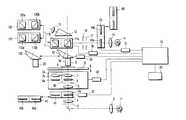
- A first embodiment of the present invention will now be described with reference to FIGS. 1 and 2. In an optical system of a microscope, light from a[0020]
light source 1 for transmissive illumination, e.g., a halogen lamp, is condensed by means of acollector lens 2 and transmitted through atransmissive field stop 3, and then lands on afilter turret 4 for transmission that can be inserted into and removed from the body of the microscope. Thefilter turret 4 is fitted with six different filters for six-stage change-over. These filers include, for example, anND filter 4afor adjusting the brightness of thelight source 1 for transmission without changing its color temperature, a compensatingfilter 4bfor color correction. Desired filters can be alternatively inserted into and removed from the lighting optical system. - Illumination light transmitted through the[0021]
filter turret 4 for transmission is guided through atransmissive aperture stop 5, condenseroptical element unit 6, and condensertop lens unit 7 and applied to a specimen S on aspecimen stage 8 from under thestage 8. The condenseroptical element unit 6 is composed of sixdifferent condensers 6ato6f(of which6cto6fare not shown) that can be alternatively inserted into and removed from the optical path. The condensertop lens unit 7 is composed of a plurality of condensertop lenses specimen stage 8 can two-dimensionally move the specimen S within a plane that extends at right angles to the optical axis of the microscope and vertically move for focusing along the optical axis. - Above the[0022]
specimen stage 8, moreover, a six-stage revolver 10 that can be loaded with six differentobjective lenses 9ato9f(of which9bto9fare not shown) is removably held for rotation on the lower surface of an arm end portion (not shown) of the microscope. Any of theobjective lenses 9ato9fcan be inserted into or removed from the optical path on the optical axis in the observational light path by rotating therevolver 10. Further, acube cassette 11 is located on the optical axis on the observational light path on the upper surface of the arm end portion of the microscope. Thecube cassette 11 is in the form of a four-stage turret that is loaded with fourdifferent filter cubes 11ato11d(of which11cand11dare not shown). Any of the filter cubes can be alternatively inserted into and removed from the optical path by various microscopic methods. - Light transmitted through the[0023]
cube 11aof thecube cassette 11 is branched in two directions by means of abeam splitter 12. One of the resulting branch light beam is guided to aneyepiece 13, and the other to a photographic optical path (not shown). - Further, light from a[0024]
light source 14 for incident illumination, formed of a mercury vapor lamp, is condensed by means of acollector lens 15, and landed on an incidentlight filter turret 16 that is changeably attached to the microscope body (not shown). Thefilter turret 16, which is changeable in six stages, is fitted with sixdifferent filters 16ato16f(of which16cto16fare not shown). Thefilter 16ais an ND filter for adjusting the brightness of thelight source 14 for incident illumination without changing its color temperature, while thefilter 16bis a compensating filter for color correction. Any of thefilters 16ato16fcan be alternatively inserted into and removed from the optical path. - Light from the[0025]
light source 14 for incident illumination is guided through theND filter 16a, anincident aperture stop 17, and anincident field stop 18. The light is refracted downward by means of afilter cube 11athat is inserted in the optical path, and is landed on the specimen S to illuminate it through theobjective lens 9a. Fluorescent light or reflected observational light from the illuminated specimen S is transmitted again through theobjective lens 9aand thecube cassette 11 and branched by means of thebeam splitter 12. One of the resulting branch beams is guided to theeyepiece 13, and the other to the photographic optical path (not shown). - A[0026]
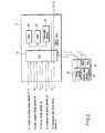
control section 19 and anoperating section 20 shown in FIG. 1 will now be described with reference to FIG. 2. - The[0027]
control section 19 is composed of aCPU 21,ROM 22,RAM 23, andnonvolatile memory 24, which are connected to one another by means of their respective CPU buses. TheROM 22 is stored with programs in which control contents are described, while theRAM 23 is loaded with data for control operation. Thenonvolatile memory 24, which may be an EEPROMM, NVRAM, or flash memory, stores or reads necessary information as the programs are executed. - The[0028]
operating section 20 is formed of adisplay element 25 and aswitch input element 26, which are connected to theCPU 21. The operatingsection 20 delivers an operation signal from theswitch input element 26 to theCPU 21, and controls position information on various drivingelements 27 to31 (mentioned later). - Further, the[0029]
control section 19 is provided with an external I/F (not shown) such as an RS-232C, USB, or Ethernet. When it receives a command from an external controller such as a PC through the I/F, thecontrol section 19 can carry out driving element control that is equivalent to operation through the operatingsection 20. - The following is a description of the driving[0030]
elements 27 to31. - In response to a driving signal from the[0031]
control section 19, the transmissive filterturret driving element 27 rotates thetransmissive filter turret 4, thereby alternatively inserting into or removing one offilters 4ato4ffrom the optical path. - In response to a driving signal from the[0032]
control section 19, a condenserunit driving element 28 carries out stop adjustment for thetransmissive aperture stop 5, and rotates the condenseroptical element unit 6 and the condensertop lens unit 7, thereby alternatively inserting into or removing the desiredoptical element top lens - In response to a driving signal from the[0033]
control section 19, arevolver driving element 29 rotates therevolver 10, thereby alternatively inserting into or removing one of theobjective lenses 9ato9ffrom the optical path. - In response to a driving signal from the[0034]
control section 19, a cubecassette driving element 30 rotates thecube cassette 11, thereby alternatively inserting into or removing one of thefilter cubes 11ato11dfrom the optical path. - In response to a driving signal from the[0035]
control section 19, an incident filterturret driving element 31 rotates theincident filter turret 16, thereby alternatively inserting into or removing one of thefilters 16ato16ffrom the optical path. - The cube[0036]
cassette driving element 30 will further be described with reference to FIGS. 3 and 4. FIGS. 3 and 4 are a front view and a side view, respectively, of thecube cassette 11. In thecube cassette 11, thecubes 11ato11dare arranged at equal spaces on the circumference of a circle on a disc11-1. The disc11-1 is rotated by means of a pulse motor30-1 of the cubecassette driving element 30. A magnet11-2 for detecting the origin position of the disc11-1 is attached to the outer peripheral surface of the disc11-1. A Hall element30-2 of the cubecassette driving element 30 is located in a position opposite to the magnet11-2. Corresponding in position to thecubes 11ato11d, respectively, moreover, openings11-3 to11-6 are provided on the outer periphery of the disc11-1. The openings11-3 to11-6 are used to detect positioning of thecubes 11ato11don an optical path OP. Held on the cubecassette driving element 30, furthermore, is a photo-interrupter30-3, which detects the openings11-3 to11-6. When thefilter cube 11cis located on the optical path OP, correct positioning of thecube 11con the optical path OP can be detected by detecting the presence of the opening11-5 by means of the photo-interrupter30-3. - The[0037]
filter turret 4,revolver 10, andincident filter turret 16, like thecube cassette 11, are provided with a magnet for origin position detection and openings for positioning detection each. Like the cubecassette driving element 30, moreover, the transmissive filterturret driving element 27, condenserunit driving element 28, andrevolver driving element 29 are provided with a Hall element and a photo-interrupter each. Thus, the origin position and the optical elements that are situated on the optical path can be detected. - The searching operation of the[0038]
cube cassette 11 will now be described with reference to the flowchart of FIG. 7. - First, the[0039]
control section 19 is started to clear the count number in a counter (not shown) (C:0; Step S1). Thereafter, the disc11-1 is rotated by means of the cube cassette driving element30 (Step S2). As the disc11-1 rotates in this manner, the position of the magnet11-2 on the disc11-1 is detected by means of the Hall element30-2. If the origin position of the disc11-1 is detected by doing this (Step S3), counting detected positioning signals is started (Step S4). As the disc11-1 further rotates so that the opening11-5 is detected by means of the photo-interrupter30-3, the positioning signals are detected, and the count C is upped (C:1; Step S5). - Further, counting the positioning signals for the disc[0040]11-1 is continued. As the disc11-1 then rotates, the opening11-4 reaches the photo-interrupter30-3, whereupon the count C is upped (C:2; Step S5). Likewise, the detected positioning signals for the openings11-3 and11-6 continue to be counted in succession, and the count C is upped (C:3, C:4; Step S5) on each occasion.
- If the disc[0041]11-1 further continues to be rotated, the magnet11-2 that is held on the disc11-1 is detected again by means of the Hall element30-2 that is held in the cube
cassette driving element 30, and therefore, the origin position of the disc11-1 is detected again (Step S6), whereupon the rotation of the disc11-1 stops (Step S7). Then, the count (C:4) is loaded into thenonvolatile memory 24, whereupon the searching operation is finished. The number of change-over stages (four stages) of thecube cassette 11 can be detected by examining the value of the count C. - FIG. 5 shows a six-[0042]
stage cube cassette 110 that is used in place of thecube cassette 11. Searching operation with use of thecube cassette 110 will now be described with reference to the flowchart of FIG. 7. - In the[0043]
cube cassette 110, a magnet110-2 for origin detection is attached to the peripheral edge of the disc110-1, sixdifferent cubes 110a to10f are placed on the disc110-1, and openings110-3 to110-8 are provided corresponding to thecubes 110ato110f, respectively. - The[0044]
control section 19 starts the searching operation for thecube cassette 110. First, the count number in the counter (not shown) is cleared (C:0; Step S1). Thereafter, the disc110-1 is rotated by means of the cube cassette driving element30 (Step S2). As the disc110-1 rotates in this manner, the position of the magnet110-2 on the disc110-1 is detected by means of the Hall element30-2. If the origin position of the disc110-1 is detected by doing this (Step S3), the counter starts counting detected positioning signals (Step S4). As the disc110-1 further rotates so that the opening110-6 is detected by means of the photo-interrupter30-3, the positioning signals are detected, and the count C is upped (C:1; Step S5). Further, counting the positioning signals for the disc110-1 is continued. If the opening110-5 is detected by means of the photo-interrupter30-3 as the disc110-1 rotates, the count C is upped (C:2; Step S5). Likewise, the opening110-4 is detected, and the count C is upped (C:3; Step S5). Likewise, the openings110-3,110-8 and110-7 are detected, and the count C is upped (C:4, C:5, C:6; Step S5). - If the rotation of the disc[0045]110-1 is continued, moreover, the magnet110-2 held on the disc110-1 is detected again by means of the Hall element30-2 that is held in the cube
cassette driving element 30. Thereupon, the origin position of the disc110-1 is detected (Step S6), and the rotation of the disc110-1 stops (Step S7). Then, the count (C:6) is loaded into thenonvolatile memory 24, whereupon the searching operation is finished. The number of change-over stages (six stages) of thecube cassette 11 can be detected by examining the value of the count C. - FIG. 6 shows an eight-[0046]
stage cube cassette 120. For searching operation in this case, the number of change-over stages (eight stages) of thecube cassette 120 can be also detected with reference to the flowchart of FIG. 7. - In the[0047]
cube cassette 120, a magnet120-2 for origin detection is attached to the peripheral edge of a disc120-1, eightdifferent cubes 120ato120hare placed on the disc120-1, and openings120-3 to120-10 are provided corresponding to thecubes 120ato120f,respectively. - According to the first embodiment described above, the control can be started when the apparatus is switched on as the so-called initializing operation. If searching operation is started by a first cycle of change-over operation for the cube cassette based on the operation of the[0048]
operating section 20, instead of switching the apparatus on, the searching operation can be carried out only when necessary. Thus, the time that is required by the searching operation with the power on can be saved. - In connection with the first embodiment, the[0049]
cube cassettes transmissive filter turrets revolvers incident filter turrets - A second embodiment of the invention will now be described with reference to the flowchart of FIG. 8.[0050]
- An optical element change-over control apparatus and an optical microscope using the same according to the second embodiment resemble the ones according to the first embodiment. According to the second embodiment, switches[0051]100aand100bare additionally used as setting members for previously setting the
control section 19 or theoperating section 20 to settle whether or not to execute operation for detecting the point of origin of the optical element change-over member. For example, dip switches are used as the switches100i a l and100b. - The present invention will now be described in connection with the[0052]
cube cassette 11 shown in FIG. 3 with reference to the flowchart of FIG. 8. - First, the state of the[0053]
switch control section 19 or theoperating section 20 is examined (Step S1). If theswitch nonvolatile memory 24 and detected as the number of change-over stages of the cube cassette (END). If theswitch cube cassette 11 is started. After thecontrol section 19 is started to clear the count number in the counter (not shown) (C:0; Step S2), the disc11-1 is rotated by means of the cube cassette driving element30 (Step S3). As the disc11-1 rotates in this manner, the position of the magnet11-2 on the disc11-1 is detected by means of the Hall element30-2. If the origin position of the disc11-1 is detected by doing this (Step S4), counting the positioning signals is started (Step S5). As the disc11-1 further rotates so that the opening11-5 is detected by means of the photo-interrupter30-3, the positioning signals are outputted, and the count C is upped (C:1; Step S6). Further, counting the positioning signals for the disc11-1 is continued. If the opening11-4 is detected by means of the photo-interrupter30-3 as the disc11-1 rotates, the count C is upped (C:2; Step S6). Likewise, the positioning signals for the openings11-3 and11-6 continue to be counted in succession, and the count C is upped (C:3, C:4; Step S6) on each occasion. - If the disc[0054]11-1 further continues to be rotated, the magnet11-2 that is held on the disc11-1 is detected again by means of the Hall element30-2 that is held in the cube
cassette driving element 30, and therefore, the origin position of the disc11-1 is detected (Step S7), whereupon the rotation of the disc11-1 stops (Step S8). Then, the value of the count C (C:4) is loaded into thenonvolatile memory 24, whereupon the searching operation is finished (END). The number of change-over stages (four stages) of thecube cassette 11 can be obtained by examining the value of the count C. - The following is a description of optical element searching operation with use of the six-[0055]
stage cube cassette 110 of FIG. 5 in place of thecube cassette 11. - First, the state of the[0056]
switch control section 19 or theoperating section 20 is examined (Step S1). If theswitch nonvolatile memory 24, and its value is detected as the number of change-over stages of the cube cassette (END). If theswitch cube cassette 110 is started. After the count number in the counter (not shown) is first cleared (C:0; Step S2), the disc110-1 is rotated by means of the cube cassette driving element30 (Step S3). As the disc110-1 rotates in this manner, the position of the magnet110-2 on the disc110-1 is detected by means of the Hall element30-2. If the origin position of the disc110-1 is detected by doing this (Step S4), the counter starts counting the positioning signals. As the disc110-1 is further rotated so that the opening110-6 is detected by means of the photo-interrupter30-3, the positioning signals are outputted, and the count C is upped (C:1; Step S5). Further, counting the positioning signals for the disc110-1 is continued. If the opening110-5 is detected by means of the photo-interrupter30-3 as the disc110-1 rotates, the count C is upped (C:2; Step S5). Likewise, the count C is upped (C:3; Step S5) as the opening110-4 is detected by means of the photo-interrupter30-3. Likewise, moreover, the count C is upped (C:4, C:5, C:6; Step S6) as the openings110-3,110-8 and110-7 are detected in succession by means of the photo-interrupter30-3. - If the disc[0057]110-1 further continues to be rotated, the magnet110-2 that is held on the disc110-1 is detected again by means of the Hall element30-2 that is held in the cube
cassette driving element 30, and therefore, the origin position of the disc110-1 is detected (Step S7), whereupon the rotation of the disc110-1 stops (Step S8). Then, the value of the count C (C:6) is loaded into thenonvolatile memory 24, whereupon the searching operation is finished. - The number of change-over stages (six stages) of the[0058]
cube cassette 110 can be detected by examining the value of the count C. - For searching operation for the eight-[0059]
stage cube cassette 120 shown in FIG. 6, the number of change-over stages (eight stages) of thecube cassette 120 can be also detected with reference to the flowchart of FIG. 8. - The control according to second embodiment described above, like the control according to first embodiment, can be started when the apparatus is switched on as the so-called initializing operation. If searching operation is started by a first cycle of change-over operation for the cube cassette based on the operation of the[0060]
operating section 20, instead of switching the apparatus on, the searching operation can be carried out only when necessary. Thus, the time that is required by the searching operation with the power on can be saved. - In connection with the second embodiment, the[0061]
cube cassettes transmissive filter turrets revolvers incident filter turrets - According to the present invention, the optical element unit to be attached to the microscope body can be replaced. If the number of change-over stages is changed, therefore, the control function need not be changed at all. Thus, the microscope can be smoothly operated by detecting the number of change-over stages of the newly set optical element unit.[0062]
- Additional advantages and modifications will readily occur to those skilled in the art. Therefore, the invention in its broader aspects is not limited to the specific details and representative embodiments shown and described herein. Accordingly, various modifications may be made without departing from the spirit or scope of the general inventive concept as defined by the appended claims and their equivalents.[0063]
Claims (10)
Applications Claiming Priority (2)
| Application Number | Priority Date | Filing Date | Title |
|---|---|---|---|
| JP2000224345AJP2002040330A (en) | 2000-07-25 | 2000-07-25 | Optical element changeover controller |
| JP2000-224345 | 2000-07-25 |
Publications (2)
| Publication Number | Publication Date |
|---|---|
| US20020097486A1true US20020097486A1 (en) | 2002-07-25 |
| US6636353B2 US6636353B2 (en) | 2003-10-21 |
Family
ID=18718328
Family Applications (1)
| Application Number | Title | Priority Date | Filing Date |
|---|---|---|---|
| US09/910,740Expired - LifetimeUS6636353B2 (en) | 2000-07-25 | 2001-07-23 | Optical element change-over control apparatus and microscope using the same |
Country Status (2)
| Country | Link |
|---|---|
| US (1) | US6636353B2 (en) |
| JP (1) | JP2002040330A (en) |
Cited By (46)
| Publication number | Priority date | Publication date | Assignee | Title |
|---|---|---|---|---|
| US20040080817A1 (en)* | 2002-09-17 | 2004-04-29 | Olympus Optical Co., Ltd. | Electric optical microscope |
| EP1512998A1 (en)* | 2003-09-04 | 2005-03-09 | Olympus Corporation | Optical microscope apparatus, optical element arranging method, and storage medium |
| US20050132914A1 (en)* | 2003-12-23 | 2005-06-23 | Asml Netherlands B.V. | Lithographic apparatus, alignment apparatus, device manufacturing method, and a method of converting an apparatus |
| US20060012860A1 (en)* | 2004-07-19 | 2006-01-19 | Leica Microsystems Cms Gmbh | Indexable microscope |
| US20080297647A1 (en)* | 2007-06-04 | 2008-12-04 | Olympus Corporation | Image pickup device |
| DE102007045556A1 (en)* | 2007-09-24 | 2009-04-02 | Carl Zeiss Microimaging Gmbh | By light microscope |
| DE102009017710A1 (en)* | 2009-04-14 | 2010-10-21 | Carl Zeiss Surgical Gmbh | An optical observation device and method for ensuring a constant illumination intensity when the color temperature of the illumination changes |
| US20120050851A1 (en)* | 2010-08-30 | 2012-03-01 | Leica Microsystems Cms Gmbh | Microscope Including Micro and Macro Objectives |
| EP1763692B1 (en)* | 2004-07-06 | 2013-03-13 | Carl Zeiss Microscopy GmbH | Microscope with a replacement device for optical elements |
| WO2016010954A3 (en)* | 2014-07-14 | 2016-05-19 | Corning Incorporated | System for and method of processing transparent materials using laser beam focal lines adjustable in length and diameter |
| US9676167B2 (en) | 2013-12-17 | 2017-06-13 | Corning Incorporated | Laser processing of sapphire substrate and related applications |
| US9701563B2 (en) | 2013-12-17 | 2017-07-11 | Corning Incorporated | Laser cut composite glass article and method of cutting |
| US9815144B2 (en) | 2014-07-08 | 2017-11-14 | Corning Incorporated | Methods and apparatuses for laser processing materials |
| US9815730B2 (en) | 2013-12-17 | 2017-11-14 | Corning Incorporated | Processing 3D shaped transparent brittle substrate |
| US9850160B2 (en) | 2013-12-17 | 2017-12-26 | Corning Incorporated | Laser cutting of display glass compositions |
| US9850159B2 (en) | 2012-11-20 | 2017-12-26 | Corning Incorporated | High speed laser processing of transparent materials |
| US20180136448A1 (en)* | 2016-11-12 | 2018-05-17 | Caliber Imaging & Diagnostics, Inc. | Confocal microscope with positionable imaging head |
| US10047001B2 (en) | 2014-12-04 | 2018-08-14 | Corning Incorporated | Glass cutting systems and methods using non-diffracting laser beams |
| US10144093B2 (en) | 2013-12-17 | 2018-12-04 | Corning Incorporated | Method for rapid laser drilling of holes in glass and products made therefrom |
| US10173916B2 (en) | 2013-12-17 | 2019-01-08 | Corning Incorporated | Edge chamfering by mechanically processing laser cut glass |
| US10233112B2 (en) | 2013-12-17 | 2019-03-19 | Corning Incorporated | Laser processing of slots and holes |
| US10252931B2 (en) | 2015-01-12 | 2019-04-09 | Corning Incorporated | Laser cutting of thermally tempered substrates |
| US10280108B2 (en) | 2013-03-21 | 2019-05-07 | Corning Laser Technologies GmbH | Device and method for cutting out contours from planar substrates by means of laser |
| US10335902B2 (en) | 2014-07-14 | 2019-07-02 | Corning Incorporated | Method and system for arresting crack propagation |
| US10377658B2 (en) | 2016-07-29 | 2019-08-13 | Corning Incorporated | Apparatuses and methods for laser processing |
| US10421683B2 (en) | 2013-01-15 | 2019-09-24 | Corning Laser Technologies GmbH | Method and device for the laser-based machining of sheet-like substrates |
| CN110361859A (en)* | 2018-09-03 | 2019-10-22 | 上海北昂医药科技股份有限公司 | Object lens control device based on Hall switch |
| US10522963B2 (en) | 2016-08-30 | 2019-12-31 | Corning Incorporated | Laser cutting of materials with intensity mapping optical system |
| US10526234B2 (en) | 2014-07-14 | 2020-01-07 | Corning Incorporated | Interface block; system for and method of cutting a substrate being transparent within a range of wavelengths using such interface block |
| US10525657B2 (en) | 2015-03-27 | 2020-01-07 | Corning Incorporated | Gas permeable window and method of fabricating the same |
| US10611667B2 (en) | 2014-07-14 | 2020-04-07 | Corning Incorporated | Method and system for forming perforations |
| US10626040B2 (en) | 2017-06-15 | 2020-04-21 | Corning Incorporated | Articles capable of individual singulation |
| US10688599B2 (en) | 2017-02-09 | 2020-06-23 | Corning Incorporated | Apparatus and methods for laser processing transparent workpieces using phase shifted focal lines |
| US10730783B2 (en) | 2016-09-30 | 2020-08-04 | Corning Incorporated | Apparatuses and methods for laser processing transparent workpieces using non-axisymmetric beam spots |
| US10752534B2 (en) | 2016-11-01 | 2020-08-25 | Corning Incorporated | Apparatuses and methods for laser processing laminate workpiece stacks |
| US11062986B2 (en) | 2017-05-25 | 2021-07-13 | Corning Incorporated | Articles having vias with geometry attributes and methods for fabricating the same |
| US11078112B2 (en) | 2017-05-25 | 2021-08-03 | Corning Incorporated | Silica-containing substrates with vias having an axially variable sidewall taper and methods for forming the same |
| US11111170B2 (en) | 2016-05-06 | 2021-09-07 | Corning Incorporated | Laser cutting and removal of contoured shapes from transparent substrates |
| US11114309B2 (en) | 2016-06-01 | 2021-09-07 | Corning Incorporated | Articles and methods of forming vias in substrates |
| US11186060B2 (en) | 2015-07-10 | 2021-11-30 | Corning Incorporated | Methods of continuous fabrication of holes in flexible substrate sheets and products relating to the same |
| US11542190B2 (en) | 2016-10-24 | 2023-01-03 | Corning Incorporated | Substrate processing station for laser-based machining of sheet-like glass substrates |
| US11554984B2 (en) | 2018-02-22 | 2023-01-17 | Corning Incorporated | Alkali-free borosilicate glasses with low post-HF etch roughness |
| US11556039B2 (en) | 2013-12-17 | 2023-01-17 | Corning Incorporated | Electrochromic coated glass articles and methods for laser processing the same |
| US11774233B2 (en) | 2016-06-29 | 2023-10-03 | Corning Incorporated | Method and system for measuring geometric parameters of through holes |
| US11773004B2 (en) | 2015-03-24 | 2023-10-03 | Corning Incorporated | Laser cutting and processing of display glass compositions |
| US12180108B2 (en) | 2017-12-19 | 2024-12-31 | Corning Incorporated | Methods for etching vias in glass-based articles employing positive charge organic molecules |
Families Citing this family (11)
| Publication number | Priority date | Publication date | Assignee | Title |
|---|---|---|---|---|
| DE10257521B4 (en)* | 2002-12-10 | 2017-03-30 | Leica Microsystems Cms Gmbh | reflected light microscope |
| JP4678818B2 (en)* | 2004-04-28 | 2011-04-27 | オリンパス株式会社 | Microscope transmitted illumination device |
| JP4590207B2 (en)* | 2004-05-14 | 2010-12-01 | オリンパス株式会社 | Microscope equipment |
| JP2006276193A (en)* | 2005-03-28 | 2006-10-12 | Nikon Corp | microscope |
| JP4744963B2 (en)* | 2005-07-22 | 2011-08-10 | Hoya株式会社 | Lens barrel |
| JP4937768B2 (en)* | 2007-01-16 | 2012-05-23 | オリンパス株式会社 | System microscope control apparatus and unit recognition method thereof |
| JP4974717B2 (en)* | 2007-03-12 | 2012-07-11 | オリンパス株式会社 | Corrector ring driving device for objective lens with microscope correction ring |
| DE102007027084B4 (en)* | 2007-06-12 | 2021-01-14 | Carl Zeiss Microscopy Gmbh | Microscope for observing a sample using the bright field transmitted light or fluorescence incident light contrast method |
| WO2010111649A1 (en)* | 2009-03-26 | 2010-09-30 | Guy Kennedy | Low numerical aperture exclusion imaging |
| US9703087B2 (en)* | 2015-02-17 | 2017-07-11 | Echo Laboratories, Inc. | Fluorescence module with a plurality of filters and light sources |
| CN110531477A (en)* | 2019-08-30 | 2019-12-03 | 北京临近空间飞行器系统工程研究所 | A kind of multicomponent high density filling device |
Family Cites Families (6)
| Publication number | Priority date | Publication date | Assignee | Title |
|---|---|---|---|---|
| DE3410201A1 (en)* | 1983-03-22 | 1984-10-04 | Olympus Optical Co., Ltd., Tokio/Tokyo | MICROSCOPE |
| US4843292A (en)* | 1987-03-02 | 1989-06-27 | Yokogawa Electric Corporation | Direct drive motor system |
| US5396063A (en)* | 1992-06-08 | 1995-03-07 | Nikon Corporation | Objective replacing apparatus having objective position, displacement and address detecting means and microscope using it |
| JPH08179218A (en) | 1994-12-27 | 1996-07-12 | Olympus Optical Co Ltd | Microscope system |
| JP3537205B2 (en)* | 1995-02-02 | 2004-06-14 | オリンパス株式会社 | Microscope equipment |
| US6219180B1 (en)* | 1999-04-13 | 2001-04-17 | Olympus America, Inc. | Optical unit switching apparatus |
- 2000
- 2000-07-25JPJP2000224345Apatent/JP2002040330A/ennot_activeWithdrawn
- 2001
- 2001-07-23USUS09/910,740patent/US6636353B2/ennot_activeExpired - Lifetime
Cited By (72)
| Publication number | Priority date | Publication date | Assignee | Title |
|---|---|---|---|---|
| US20040080817A1 (en)* | 2002-09-17 | 2004-04-29 | Olympus Optical Co., Ltd. | Electric optical microscope |
| USRE42948E1 (en) | 2003-09-04 | 2011-11-22 | Olympus Corporation | Optical microscope apparatus, optical element arranging method, and storage medium |
| EP1512998A1 (en)* | 2003-09-04 | 2005-03-09 | Olympus Corporation | Optical microscope apparatus, optical element arranging method, and storage medium |
| US7224522B2 (en) | 2003-09-04 | 2007-05-29 | Olympus Corporation | Optical microscope apparatus, optical element arranging method, and storage medium |
| US20050132914A1 (en)* | 2003-12-23 | 2005-06-23 | Asml Netherlands B.V. | Lithographic apparatus, alignment apparatus, device manufacturing method, and a method of converting an apparatus |
| US20090296061A1 (en)* | 2003-12-23 | 2009-12-03 | Asml Netherlands B.V. | Lithographic apparatus, alignment apparatus, device manufacturing method, and a method of converting an apparatus |
| EP1763692B1 (en)* | 2004-07-06 | 2013-03-13 | Carl Zeiss Microscopy GmbH | Microscope with a replacement device for optical elements |
| US20060012860A1 (en)* | 2004-07-19 | 2006-01-19 | Leica Microsystems Cms Gmbh | Indexable microscope |
| US7440183B2 (en)* | 2004-07-19 | 2008-10-21 | Leica Microsystems Cms Gmbh | Indexable microscope |
| US7929041B2 (en)* | 2007-06-04 | 2011-04-19 | Olympus Corporation | Image pickup device |
| US20080297647A1 (en)* | 2007-06-04 | 2008-12-04 | Olympus Corporation | Image pickup device |
| DE102007045556A1 (en)* | 2007-09-24 | 2009-04-02 | Carl Zeiss Microimaging Gmbh | By light microscope |
| DE102009017710B4 (en)* | 2009-04-14 | 2019-10-31 | Carl Zeiss Meditec Ag | An optical observation device and method for ensuring a constant illumination intensity when the color temperature of the illumination changes |
| DE102009017710A1 (en)* | 2009-04-14 | 2010-10-21 | Carl Zeiss Surgical Gmbh | An optical observation device and method for ensuring a constant illumination intensity when the color temperature of the illumination changes |
| US9829692B2 (en) | 2009-04-14 | 2017-11-28 | Carl Zeiss Meditec Ag | Optical observation unit and method for ensuring an unchanging illumination intensity when changing the color temperature of the illumination |
| US20120050851A1 (en)* | 2010-08-30 | 2012-03-01 | Leica Microsystems Cms Gmbh | Microscope Including Micro and Macro Objectives |
| US8964289B2 (en)* | 2010-08-30 | 2015-02-24 | Leica Microsystems Cms Gmbh | Microscope including micro and macro objectives |
| US9850159B2 (en) | 2012-11-20 | 2017-12-26 | Corning Incorporated | High speed laser processing of transparent materials |
| US10421683B2 (en) | 2013-01-15 | 2019-09-24 | Corning Laser Technologies GmbH | Method and device for the laser-based machining of sheet-like substrates |
| US11028003B2 (en) | 2013-01-15 | 2021-06-08 | Corning Laser Technologies GmbH | Method and device for laser-based machining of flat substrates |
| US11345625B2 (en) | 2013-01-15 | 2022-05-31 | Corning Laser Technologies GmbH | Method and device for the laser-based machining of sheet-like substrates |
| US11713271B2 (en) | 2013-03-21 | 2023-08-01 | Corning Laser Technologies GmbH | Device and method for cutting out contours from planar substrates by means of laser |
| US10280108B2 (en) | 2013-03-21 | 2019-05-07 | Corning Laser Technologies GmbH | Device and method for cutting out contours from planar substrates by means of laser |
| US9701563B2 (en) | 2013-12-17 | 2017-07-11 | Corning Incorporated | Laser cut composite glass article and method of cutting |
| US9850160B2 (en) | 2013-12-17 | 2017-12-26 | Corning Incorporated | Laser cutting of display glass compositions |
| US11148225B2 (en) | 2013-12-17 | 2021-10-19 | Corning Incorporated | Method for rapid laser drilling of holes in glass and products made therefrom |
| US10144093B2 (en) | 2013-12-17 | 2018-12-04 | Corning Incorporated | Method for rapid laser drilling of holes in glass and products made therefrom |
| US10173916B2 (en) | 2013-12-17 | 2019-01-08 | Corning Incorporated | Edge chamfering by mechanically processing laser cut glass |
| US10179748B2 (en) | 2013-12-17 | 2019-01-15 | Corning Incorporated | Laser processing of sapphire substrate and related applications |
| US10233112B2 (en) | 2013-12-17 | 2019-03-19 | Corning Incorporated | Laser processing of slots and holes |
| US9815730B2 (en) | 2013-12-17 | 2017-11-14 | Corning Incorporated | Processing 3D shaped transparent brittle substrate |
| US11556039B2 (en) | 2013-12-17 | 2023-01-17 | Corning Incorporated | Electrochromic coated glass articles and methods for laser processing the same |
| US10293436B2 (en) | 2013-12-17 | 2019-05-21 | Corning Incorporated | Method for rapid laser drilling of holes in glass and products made therefrom |
| US10611668B2 (en) | 2013-12-17 | 2020-04-07 | Corning Incorporated | Laser cut composite glass article and method of cutting |
| US10597321B2 (en) | 2013-12-17 | 2020-03-24 | Corning Incorporated | Edge chamfering methods |
| US10392290B2 (en) | 2013-12-17 | 2019-08-27 | Corning Incorporated | Processing 3D shaped transparent brittle substrate |
| US9676167B2 (en) | 2013-12-17 | 2017-06-13 | Corning Incorporated | Laser processing of sapphire substrate and related applications |
| US10442719B2 (en) | 2013-12-17 | 2019-10-15 | Corning Incorporated | Edge chamfering methods |
| US9815144B2 (en) | 2014-07-08 | 2017-11-14 | Corning Incorporated | Methods and apparatuses for laser processing materials |
| US11697178B2 (en) | 2014-07-08 | 2023-07-11 | Corning Incorporated | Methods and apparatuses for laser processing materials |
| US20170189991A1 (en)* | 2014-07-14 | 2017-07-06 | Corning Incorporated | Systems and methods for processing transparent materials using adjustable laser beam focal lines |
| US10526234B2 (en) | 2014-07-14 | 2020-01-07 | Corning Incorporated | Interface block; system for and method of cutting a substrate being transparent within a range of wavelengths using such interface block |
| WO2016010954A3 (en)* | 2014-07-14 | 2016-05-19 | Corning Incorporated | System for and method of processing transparent materials using laser beam focal lines adjustable in length and diameter |
| US10611667B2 (en) | 2014-07-14 | 2020-04-07 | Corning Incorporated | Method and system for forming perforations |
| US10335902B2 (en) | 2014-07-14 | 2019-07-02 | Corning Incorporated | Method and system for arresting crack propagation |
| US11648623B2 (en)* | 2014-07-14 | 2023-05-16 | Corning Incorporated | Systems and methods for processing transparent materials using adjustable laser beam focal lines |
| US10047001B2 (en) | 2014-12-04 | 2018-08-14 | Corning Incorporated | Glass cutting systems and methods using non-diffracting laser beams |
| US11014845B2 (en) | 2014-12-04 | 2021-05-25 | Corning Incorporated | Method of laser cutting glass using non-diffracting laser beams |
| US10252931B2 (en) | 2015-01-12 | 2019-04-09 | Corning Incorporated | Laser cutting of thermally tempered substrates |
| US11773004B2 (en) | 2015-03-24 | 2023-10-03 | Corning Incorporated | Laser cutting and processing of display glass compositions |
| US10525657B2 (en) | 2015-03-27 | 2020-01-07 | Corning Incorporated | Gas permeable window and method of fabricating the same |
| US11186060B2 (en) | 2015-07-10 | 2021-11-30 | Corning Incorporated | Methods of continuous fabrication of holes in flexible substrate sheets and products relating to the same |
| US11111170B2 (en) | 2016-05-06 | 2021-09-07 | Corning Incorporated | Laser cutting and removal of contoured shapes from transparent substrates |
| US11114309B2 (en) | 2016-06-01 | 2021-09-07 | Corning Incorporated | Articles and methods of forming vias in substrates |
| US11774233B2 (en) | 2016-06-29 | 2023-10-03 | Corning Incorporated | Method and system for measuring geometric parameters of through holes |
| US10377658B2 (en) | 2016-07-29 | 2019-08-13 | Corning Incorporated | Apparatuses and methods for laser processing |
| US10522963B2 (en) | 2016-08-30 | 2019-12-31 | Corning Incorporated | Laser cutting of materials with intensity mapping optical system |
| US10730783B2 (en) | 2016-09-30 | 2020-08-04 | Corning Incorporated | Apparatuses and methods for laser processing transparent workpieces using non-axisymmetric beam spots |
| US11130701B2 (en) | 2016-09-30 | 2021-09-28 | Corning Incorporated | Apparatuses and methods for laser processing transparent workpieces using non-axisymmetric beam spots |
| US11542190B2 (en) | 2016-10-24 | 2023-01-03 | Corning Incorporated | Substrate processing station for laser-based machining of sheet-like glass substrates |
| US10752534B2 (en) | 2016-11-01 | 2020-08-25 | Corning Incorporated | Apparatuses and methods for laser processing laminate workpiece stacks |
| US20180136448A1 (en)* | 2016-11-12 | 2018-05-17 | Caliber Imaging & Diagnostics, Inc. | Confocal microscope with positionable imaging head |
| US10935778B2 (en)* | 2016-11-12 | 2021-03-02 | Caliber Imaging & Diagnostics, Inc. | Confocal microscope with positionable imaging head |
| US11796786B2 (en) | 2016-11-12 | 2023-10-24 | Caliber Imaging & Diagnostics, Inc. | Confocal microscope with positionable imaging head |
| US10688599B2 (en) | 2017-02-09 | 2020-06-23 | Corning Incorporated | Apparatus and methods for laser processing transparent workpieces using phase shifted focal lines |
| US11062986B2 (en) | 2017-05-25 | 2021-07-13 | Corning Incorporated | Articles having vias with geometry attributes and methods for fabricating the same |
| US11078112B2 (en) | 2017-05-25 | 2021-08-03 | Corning Incorporated | Silica-containing substrates with vias having an axially variable sidewall taper and methods for forming the same |
| US11972993B2 (en) | 2017-05-25 | 2024-04-30 | Corning Incorporated | Silica-containing substrates with vias having an axially variable sidewall taper and methods for forming the same |
| US10626040B2 (en) | 2017-06-15 | 2020-04-21 | Corning Incorporated | Articles capable of individual singulation |
| US12180108B2 (en) | 2017-12-19 | 2024-12-31 | Corning Incorporated | Methods for etching vias in glass-based articles employing positive charge organic molecules |
| US11554984B2 (en) | 2018-02-22 | 2023-01-17 | Corning Incorporated | Alkali-free borosilicate glasses with low post-HF etch roughness |
| CN110361859A (en)* | 2018-09-03 | 2019-10-22 | 上海北昂医药科技股份有限公司 | Object lens control device based on Hall switch |
Also Published As
| Publication number | Publication date |
|---|---|
| JP2002040330A (en) | 2002-02-06 |
| US6636353B2 (en) | 2003-10-21 |
Similar Documents
| Publication | Publication Date | Title |
|---|---|---|
| US6636353B2 (en) | Optical element change-over control apparatus and microscope using the same | |
| USRE42948E1 (en) | Optical microscope apparatus, optical element arranging method, and storage medium | |
| US6400501B2 (en) | Optical microscope | |
| US6898004B2 (en) | Microscope system | |
| US6927903B2 (en) | Rapidly changing dichroic beamsplitter | |
| US6337767B1 (en) | Microscope with visible and ultraviolet light illumination systems | |
| US20040080817A1 (en) | Electric optical microscope | |
| KR20020001892A (en) | Microscope unit | |
| JP5267161B2 (en) | Microscope equipment | |
| US4807980A (en) | Universal condenser having only a single turret for a microscope | |
| JP3497229B2 (en) | Microscope system | |
| US20080231973A1 (en) | Mechanism for a microscope objective changer and filter changer | |
| JP3745034B2 (en) | Microscope system | |
| US20050275938A1 (en) | Microscope illumination intensity measuring device | |
| JP2008003331A (en) | Microscope apparatus | |
| JP4477181B2 (en) | Microscope equipment | |
| US20130286473A1 (en) | Inverted microscope | |
| JP2002196218A (en) | Microscope | |
| JP2005128443A (en) | microscope | |
| US20090073551A1 (en) | Electrically-operated microscope | |
| JP4937768B2 (en) | System microscope control apparatus and unit recognition method thereof | |
| JP3176678B2 (en) | Microscope lighting device | |
| US20050099679A1 (en) | Microscope especially inverted microscope | |
| JPH1068888A (en) | Microscopic device | |
| JP2003084203A (en) | Microscope equipment |
Legal Events
| Date | Code | Title | Description |
|---|---|---|---|
| AS | Assignment | Owner name:OLYMPUS OPTICAL CO., LTD., JAPAN Free format text:ASSIGNMENT OF ASSIGNORS INTEREST;ASSIGNORS:YAMAGUCHI, KATSUYOSHI;SAITO, MITSUHIKO;REEL/FRAME:012344/0395 Effective date:20010718 | |
| FEPP | Fee payment procedure | Free format text:PAYOR NUMBER ASSIGNED (ORIGINAL EVENT CODE: ASPN); ENTITY STATUS OF PATENT OWNER: LARGE ENTITY | |
| STCF | Information on status: patent grant | Free format text:PATENTED CASE | |
| FEPP | Fee payment procedure | Free format text:PAYOR NUMBER ASSIGNED (ORIGINAL EVENT CODE: ASPN); ENTITY STATUS OF PATENT OWNER: LARGE ENTITY Free format text:PAYER NUMBER DE-ASSIGNED (ORIGINAL EVENT CODE: RMPN); ENTITY STATUS OF PATENT OWNER: LARGE ENTITY | |
| FPAY | Fee payment | Year of fee payment:4 | |
| FPAY | Fee payment | Year of fee payment:8 | |
| FPAY | Fee payment | Year of fee payment:12 | |
| AS | Assignment | Owner name:OLYMPUS CORPORATION, JAPAN Free format text:CHANGE OF ADDRESS;ASSIGNOR:OLYMPUS CORPORATION;REEL/FRAME:039344/0502 Effective date:20160401 |