US20020089038A1 - Fully-depleted-collector silicon-on-insulator (SOI) bipolar transistor useful alone or in SOI BiCMOS - Google Patents
Fully-depleted-collector silicon-on-insulator (SOI) bipolar transistor useful alone or in SOI BiCMOSDownload PDFInfo
- Publication number
- US20020089038A1 US20020089038A1US09/757,965US75796501AUS2002089038A1US 20020089038 A1US20020089038 A1US 20020089038A1US 75796501 AUS75796501 AUS 75796501AUS 2002089038 A1US2002089038 A1US 2002089038A1
- Authority
- US
- United States
- Prior art keywords
- type
- bipolar transistors
- substrate
- insulating layer
- forming
- Prior art date
- Legal status (The legal status is an assumption and is not a legal conclusion. Google has not performed a legal analysis and makes no representation as to the accuracy of the status listed.)
- Granted
Links
- 239000012212insulatorSubstances0.000titleabstractdescription18
- 239000000758substrateSubstances0.000claimsabstractdescription58
- 239000004065semiconductorSubstances0.000claimsabstractdescription54
- 238000000034methodMethods0.000claimsdescription19
- 239000013078crystalSubstances0.000claimsdescription10
- 239000002019doping agentSubstances0.000claimsdescription8
- 229910000577Silicon-germaniumInorganic materials0.000claimsdescription4
- LEVVHYCKPQWKOP-UHFFFAOYSA-N[Si].[Ge]Chemical group[Si].[Ge]LEVVHYCKPQWKOP-UHFFFAOYSA-N0.000claimsdescription3
- 229910045601alloyInorganic materials0.000claimsdescription3
- 239000000956alloySubstances0.000claimsdescription3
- 238000000059patterningMethods0.000claims4
- 238000004519manufacturing processMethods0.000abstract2
- 239000000463materialSubstances0.000abstract1
- XUIMIQQOPSSXEZ-UHFFFAOYSA-NSiliconChemical compound[Si]XUIMIQQOPSSXEZ-UHFFFAOYSA-N0.000description40
- 229910021420polycrystalline siliconInorganic materials0.000description39
- 229920005591polysiliconPolymers0.000description38
- 229910052710siliconInorganic materials0.000description34
- 239000010703siliconSubstances0.000description34
- 238000002513implantationMethods0.000description8
- 239000003990capacitorSubstances0.000description7
- 230000008021depositionEffects0.000description7
- 238000005468ion implantationMethods0.000description7
- 238000002955isolationMethods0.000description6
- 230000006870functionEffects0.000description5
- 238000010586diagramMethods0.000description4
- 238000005530etchingMethods0.000description3
- 238000011049fillingMethods0.000description3
- 230000003647oxidationEffects0.000description3
- 238000007254oxidation reactionMethods0.000description3
- 238000005498polishingMethods0.000description3
- 238000002360preparation methodMethods0.000description3
- ZOXJGFHDIHLPTG-UHFFFAOYSA-NBoronChemical compound[B]ZOXJGFHDIHLPTG-UHFFFAOYSA-N0.000description2
- 230000015572biosynthetic processEffects0.000description2
- 229910052796boronInorganic materials0.000description2
- 230000000295complement effectEffects0.000description2
- 229910052732germaniumInorganic materials0.000description2
- GNPVGFCGXDBREM-UHFFFAOYSA-Ngermanium atomChemical compound[Ge]GNPVGFCGXDBREM-UHFFFAOYSA-N0.000description2
- 238000011065in-situ storageMethods0.000description2
- 230000010354integrationEffects0.000description2
- 238000001020plasma etchingMethods0.000description2
- 238000000137annealingMethods0.000description1
- 239000000969carrierSubstances0.000description1
- 230000015556catabolic processEffects0.000description1
- 238000004891communicationMethods0.000description1
- 229910021419crystalline siliconInorganic materials0.000description1
- 230000007812deficiencyEffects0.000description1
- 230000005684electric fieldEffects0.000description1
- 238000005516engineering processMethods0.000description1
- 239000012535impuritySubstances0.000description1
- 229910044991metal oxideInorganic materials0.000description1
- 150000004706metal oxidesChemical class0.000description1
- 238000012986modificationMethods0.000description1
- 230000004048modificationEffects0.000description1
Images


Classifications
- H—ELECTRICITY
- H10—SEMICONDUCTOR DEVICES; ELECTRIC SOLID-STATE DEVICES NOT OTHERWISE PROVIDED FOR
- H10D—INORGANIC ELECTRIC SEMICONDUCTOR DEVICES
- H10D84/00—Integrated devices formed in or on semiconductor substrates that comprise only semiconducting layers, e.g. on Si wafers or on GaAs-on-Si wafers
- H10D84/01—Manufacture or treatment
- H10D84/0107—Integrating at least one component covered by H10D12/00 or H10D30/00 with at least one component covered by H10D8/00, H10D10/00 or H10D18/00, e.g. integrating IGFETs with BJTs
- H10D84/0109—Integrating at least one component covered by H10D12/00 or H10D30/00 with at least one component covered by H10D8/00, H10D10/00 or H10D18/00, e.g. integrating IGFETs with BJTs the at least one component covered by H10D12/00 or H10D30/00 being a MOS device
- H—ELECTRICITY
- H10—SEMICONDUCTOR DEVICES; ELECTRIC SOLID-STATE DEVICES NOT OTHERWISE PROVIDED FOR
- H10D—INORGANIC ELECTRIC SEMICONDUCTOR DEVICES
- H10D10/00—Bipolar junction transistors [BJT]
- H10D10/01—Manufacture or treatment
- H10D10/041—Manufacture or treatment of thin-film BJTs
- H—ELECTRICITY
- H10—SEMICONDUCTOR DEVICES; ELECTRIC SOLID-STATE DEVICES NOT OTHERWISE PROVIDED FOR
- H10D—INORGANIC ELECTRIC SEMICONDUCTOR DEVICES
- H10D10/00—Bipolar junction transistors [BJT]
- H10D10/311—Thin-film BJTs
- H—ELECTRICITY
- H10—SEMICONDUCTOR DEVICES; ELECTRIC SOLID-STATE DEVICES NOT OTHERWISE PROVIDED FOR
- H10D—INORGANIC ELECTRIC SEMICONDUCTOR DEVICES
- H10D62/00—Semiconductor bodies, or regions thereof, of devices having potential barriers
- H10D62/10—Shapes, relative sizes or dispositions of the regions of the semiconductor bodies; Shapes of the semiconductor bodies
- H10D62/13—Semiconductor regions connected to electrodes carrying current to be rectified, amplified or switched, e.g. source or drain regions
- H10D62/137—Collector regions of BJTs
- H—ELECTRICITY
- H10—SEMICONDUCTOR DEVICES; ELECTRIC SOLID-STATE DEVICES NOT OTHERWISE PROVIDED FOR
- H10D—INORGANIC ELECTRIC SEMICONDUCTOR DEVICES
- H10D84/00—Integrated devices formed in or on semiconductor substrates that comprise only semiconducting layers, e.g. on Si wafers or on GaAs-on-Si wafers
- H10D84/01—Manufacture or treatment
- H10D84/02—Manufacture or treatment characterised by using material-based technologies
- H10D84/03—Manufacture or treatment characterised by using material-based technologies using Group IV technology, e.g. silicon technology or silicon-carbide [SiC] technology
- H10D84/038—Manufacture or treatment characterised by using material-based technologies using Group IV technology, e.g. silicon technology or silicon-carbide [SiC] technology using silicon technology, e.g. SiGe
- H—ELECTRICITY
- H10—SEMICONDUCTOR DEVICES; ELECTRIC SOLID-STATE DEVICES NOT OTHERWISE PROVIDED FOR
- H10D—INORGANIC ELECTRIC SEMICONDUCTOR DEVICES
- H10D86/00—Integrated devices formed in or on insulating or conducting substrates, e.g. formed in silicon-on-insulator [SOI] substrates or on stainless steel or glass substrates
- H10D86/201—Integrated devices formed in or on insulating or conducting substrates, e.g. formed in silicon-on-insulator [SOI] substrates or on stainless steel or glass substrates the substrates comprising an insulating layer on a semiconductor body, e.g. SOI
Definitions
- This inventionrelates to bipolar transistors and more particularly to a bipolar transistor structure suitable for implementation on silicon on insulator (SOI) alone or with Complementary Metal Oxide Semiconductor (CMOS) devices to provide SOI BiCMOS essential for most RF and communication products or digital products that have some critical analog components.
- SOIsilicon on insulator
- CMOSComplementary Metal Oxide Semiconductor
- High-performance bipolar transistorsare vertical bipolar transistors, as opposed to lateral bipolar transistors.
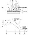
- a vertical bipolar transistorfor example an npn bipolar transistor 2 schematically shown in FIG. 1, comprises an n+ type emitter region 3 , a p type base region 4 , and an n type collector region 5 stacked one on top of the other.
- n+ type subcollector layer 6beneath the collector region 5 and an n+ type reachthrough region 7 is used to bring the collector contact to the surface.
- the emitter-base diodeis forward biased, and the base-collector diode is reverse biased.
- the entire n type collector layeris usually thick enough to accommodate the space-charge region (also called the depletion region since it is normally depleted of mobile carriers) and a quasi-neutral region.
- the thickness, or width, of the space-charge regionis determined by the collector doping concentration and the base-collector bias voltage.
- the quasi-neutral collector regioncan be very thin, usually just thick enough to prevent the space-charge region from reaching the n+ type subcollector layer. If the base-collector space-charge region touches the n+ type subcollector, it will cause the base-collector junction capacitance to increase and the base-collector junction breakdown voltage to decrease.
- the n+ type subcollector layeris usually rather thick, typically thicker than 1000 nm, in order to achieve an adequately small collector series resistance.
- FIG. 2In normal operation, electrons are injected from the emitter E and collected at the collector C.
- the dotted arrow shown in FIG. 2indicates the electron path in normal operation, starting from the emitter contact.
- FIG. 3is the energy-band diagram along the electron path.
- Aindicates the location of the emitter contact
- A′indicates the boundary between the depleted part and the quasi-neutral part of the n type collector
- A′′indicates the top of the n+ subcollector layer.
- the ordinaterepresents electron and hole energy.
- FIG. 4illustrates a vertical npn bipolar transistor 2 ′ using SOI. Usually, it is simply a vertical bipolar transistor, including its n+ type subcollector layer 6 , sitting on a buried oxide layer 9 and substrate 8 of the SOI.
- the SOI silicon layerhas to be rather thick, thick enough to accommodate the various layers of a vertical bipolar transistor described above.
- SOI BiCMOSobtained from the integration of a vertical bipolar transistor with CMOS devices using SOI has been described in a publication by Toshiro Hiramoto, et al., “A 27 GHz double polysilicon bipolar technology on bonded SOI with embedded 58 ⁇ m 2 CMOS memory cells for ECL-CMOS SRAM applications,” IEDM Technical Digest, pp. 39-42, 1992.
- the thick silicon layer needed for the bipolar transistorresults in the CMOS devices behaving like regular bulk CMOS devices, rather than like high-speed SOI CMOS devices.
- the silicon layer of high-speed SOI CMOSis usually rather thin, typically less than 200 nm, much too thin to accommodate present vertical bipolar transistor structures.
- a bipolar transistor on SOIcomprising a substrate, an insulating layer over the substrate, a first single crystal semiconductor layer positioned over the insulating layer having a lightly doped region of a first type and at least one contiguous heavily doped region of the first type, the lightly doped region and the contiguous heavily doped region functioning as a collector, a second patterned semiconductor layer of a second type formed over the lightly doped region of the first semiconductor layer to function as the base, and a third patterned semiconductor layer of the first type positioned over the second semiconductor layer to function as the emitter, the lightly doped region of the first type of the collector having a dopant concentration to fully deplete of mobile charge through the first semiconductor layer to the insulating layer of the SOI below.
- the inventionfurther provides an integrated circuit chip having both npn and pnp bipolar transistors of the above structure on SOI.
- the inventionfurther provides an integrated circuit chip having one or both npn and pnp bipolar transistors of the above structure on SOI and p-channel MOSFETs and n-channel MOSFETs wherein the source and drain regions of the MOSFETs extend downward to the insulating layer of the SOI.
- the inventionfurther provides a bipolar transistor on SOI comprising a substrate, an insulating layer over the substrate, a first single crystal semiconductor layer positioned over the insulating layer having a lightly doped region of a first type and at least one contiguous heavily doped region of the first type, the lightly doped region and the contiguous heavily doped region functioning as a collector, a top region of the lightly doped region is counter-doped to a second type to function as the base, a second patterned semiconductor layer of the second type formed over a region of the counter-doped region of the first semiconductor layer to function as the extrinsic base, and a third patterned semiconductor layer of the first type positioned over the counter-doped region of the first semiconductor layer to function as the emitter, the lightly doped region of the first type in the first semiconductor layer having a dopant concentration to fully deplete of mobile charge through the first semiconductor layer to the insulating layer of the SOI below.
- the inventionfurther provides an integrated circuit chip having both npn and pnp bipolar transistors of the above structure on SOI.
- the inventionfurther provides an integrated circuit chip having one or both npn and pnp bipolar transistors of the above structure on SOI and p-channel MOSFETs and n-channel MOSFETs wherein the source and drain regions of the MOSFETs extend downward to the insulating layer of the SOI.
- the inventionprovides a fully-depleted-collector SOI vertical bipolar transistor which has a much smaller base-collector junction capacitance than conventional devices and does not require a heavily doped subcollector layer.
- the inventionprovides an SOI bipolar transistor structure which uses thin-silicon SOI typically less than 200 nm, and is therefore readily compatible with high-speed SOI CMOS devices also using thin-silicon SOI for making high-speed SOI BiCMOS.
- FIG. 1is a cross section schematic view of a vertical bipolar transistor of the prior art.
- FIG. 2is a cross section schematic view of a vertical bipolar transistor of the prior art with the electron path shown through the transistor.
- FIG. 3is a graph of the energy-band diagram along the electron current path shown in FIG. 2.
- FIG. 4is a cross section schematic view of a vertical npn bipolar transistor using SOI of the prior art.
- FIG. 5is a cross section schematic view of an alternate vertical npn bipolar transistor structure on SOI illustrating deficiencies due to the high series resistance through the collector.
- FIG. 6is a cross section schematic view of one embodiment of the invention.
- FIG. 7is a cross section schematic view of the electron current path through the embodiment of FIG. 6.
- FIG. 8shows an energy band diagram along the electron current path shown in FIG. 7.
- FIGS. 9 - 18are cross section schematic views illustrating the steps for fabricating a fully-depleted-collector SOI vertical npn bipolar transistor having the base region formed in an epitaxially deposited silicon layer.
- FIG. 18is a cross section view along the lines 18 - 18 of FIG. 19.
- FIG. 19is a top schematic view of the transistor shown in FIG. 18.
- FIGS. 20 - 27are cross section schematic views illustrating the steps for fabricating a double-polysilicon self-aligned vertical npn bipolar transistor.
- FIGS. 28 - 39are cross section schematic views illustrating the steps for fabricating a vertical npn bipolar transistor structure shown in FIG. 18 and CMOS devices to provide SOI BiCMOS.
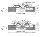
- Bipolar transistor 10has an emitter 12 of n+ type semiconductor, a base 14 of p type semiconductor and a collector 16 having a depleted n collector region 18 and a quasi-neutral n collector region 20 .
- An n+ type semiconductor region 22 contiguous with quasi-neutral n collector region 20provides a low impedance reachthrough for electrical connection to circuit wiring.
- emitter 12is over base 14 .
- Base 14is over collector region 18 and does not contact collector region 20 .
- Collector region 20is positioned between collector region 18 and n+ type semiconductor region or reachthrough 22 .
- Collector regions 18 and 20 and n+ type semiconductor region 22are positioned over buried oxide layer 26 .
- Below buried oxide layer 26is over substrate 28 .
- Silicon-on-Insulator 30comprises semiconductor regions 14 , 18 , 20 and 22 , buried oxide 26 and substrate 28 .
- Electrical contact to bipolar transistor 10may be made via contact to leads 32 , 34 and 36 which are coupled, respectively, to the emitter 12 , base 14 and collector 16 via semiconductor region 22 .
- FIG. 6shows that there is no quasi-neutral collector region 18 underneath the base region 14 .
- the collector region 18 directly underneath base 14is fully depleted.
- the n+ type reachthrough 22 , the quasi-neutral collector region 20 , and the fully-depleted collector region 18all lie on top of the buried oxide 26 of the SOI 30 .
- Position Aindicates the emitter contact 32 .
- Position A′indicates where the electrons approach the buried oxide 26 of the SOI 30 .
- Position A′′indicates where the electrons reach the quasi-neutral region 20 of collector 16 .
- the base-collector junction capacitanceis given by the usual base-collector diode space-charge layer capacitor.
- the base-collector junction capacitanceis given by two capacitors in series. They are the vertical space-charge layer capacitor and the buried oxide capacitor.
- the combined capacitanceis determined primarily by the smaller of the two capacitors.
- the base-collector junction capacitance of the fully-depleted-collector SOI transistoris determined primarily by the buried oxide capacitor. This capacitance is much smaller than the base-collector junction capacitance of a traditional vertical bipolar transistor.
- the fully-depleted-collector SOI bipolar transistor 10can be implemented with the commonly used vertical bipolar structures and processes. Thus, it can be of the double-polysilicon self-aligned type, or double-polysilicon non-self-aligned type.
- the intrinsic base layercan be formed by epitaxial deposition of silicon or by ion implantation of the silicon layer over insulator 26 of SOI 30 . With epitaxially deposited silicon for the base 14 , germanium can also be added during deposition to form a SiGe-base bipolar transistor 10 .
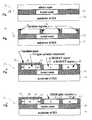
- FIGS. 9 to 18A process for fabricating a fully-depleted-collector SOI bipolar transistor 10 , using a double-polysilicon non-self-aligned structure and epitaxial deposition of silicon, or silicon-germanium (SiGe) alloy, for forming the intrinsic base is outlined in FIGS. 9 to 18 .
- the starting SOI wafer 30 shown in FIG. 9,can be prepared by any one of the common SOI preparation processes.
- Isolation oxidecan be formed by the usual masked oxidation of silicon, or by the usual shallow-trench isolation processes which involve etching silicon trenches and then filling the trenches with oxide followed by planarization using chemical-mechanical polishing.
- the resulting structureis illustrated in FIG. 10.
- a blanket implantation stepis then made to dope the n-type collector region 16 .
- the implantation stepprovides a concentration so that the n-type collector region 16 will be completely depleted when the transistor is used in circuit applications. For example, if the silicon layer thickness is 100 nm and the base-collector diode is reverse-biased at 3 V, full depletion of the collector region is assured if its average doping concentration is less than about 3 ⁇ 10 17 cm ⁇ 3 .
- a masked implantation stepis used to dope the reachthrough region 22 , which is shown as surrounding the collector region 16 , more heavily. This is illustrated in FIG. 11.
- An insulator layer 50for example an oxide layer, is deposited or formed.
- a heavily p-type doped polysilicon layer 52which will form part of the base contact polysilicon layer, is deposited. This is illustrated in FIG. 12.
- the base region windowis etched open, as shown in FIG. 13.
- a layer of silicon 54is then grown or deposited epitaxially over collector 16 .
- the deposited silicon layer 54is crystalline and forms the intrinsic base of the bipolar transistor, but over the polysilicon region 52 , the deposited silicon layer 54 is polycrystalline and simply adds to the thickness of polysilicon layer 52 .
- the intrinsic baseis doped p-type. The doping can be done by boron implantation of the deposited layer of silicon 54 , or by in situ doping of silicon layer 54 during deposition.
- the resulting transistorwill be a SiGe-base bipolar transistor.
- a layer of insulator 56for example an oxide layer, is then deposited. This is shown in FIG. 14.
- the base polysilicon layer 54is patterned, followed by an oxide deposition and reactive-ion etching to form a sidewall oxide 57 on the vertical surface of the etched polysilicon 54 , as shown in FIG. 15.
- the emitter windowis etched open, as shown in FIG. 16.
- An n+ polysilicon emitter 58is formed as shown in FIG. 17. Contact windows to the base and the collector are then etched open.
- the cross section view of a completed transistoris shown in FIG. 18.
- a top schematic view of the completed transistoris shown in FIG. 19.
- FIGS. 20 to 27A process for fabricating a double-polysilicon self-aligned bipolar transistor, using ion-implantation for forming the intrinsic base region, is outlined in FIGS. 20 to 27 .
- the starting SOI wafer 30 shown in FIG. 20,can be prepared by any of the common SOI preparation process.
- Isolation oxidecan be formed by the usual masked oxidation of silicon process, or by the usual shallow-trench isolation processes which involve etching silicon trenches and then filling the trenches with oxide followed by planarization using chemical-mechanical polishing. This is illustrated in FIG. 21.
- a blanket implantation stepis then made to dope the n-type collector region 16 .
- the implantation stepprovides a concentration so that the n-type collector region 16 will be completed depleted when the transistor is used in circuit applications.
- a masked implantation stepis used to dope more heavily the reachthrough region 22 , which is shown as surrounding the collector region 16 . This is illustrated in FIG. 22.
- An insulator layerfor example an oxide layer 60 , is deposited or formed.
- the base windowis etched open. This is illustrated in FIG. 23.
- a heavily p-type polysilicon layer 62is deposited. Polysilicon layer 62 forms the base polysilicon contact layer. It can be doped in situ during deposition, or doped by ion implantation of an undoped polysilicon layer.
- An insulator layer 64for example an oxide layer, is then deposited or formed.
- FIG. 24The base polysilicon layer 62 is patterned and a sidewall insulator layer 66 is formed on the vertical etched surface. A thermal annealing process is carried out to drive the p-type dopant from the polysilicon layer 62 into the single crystal region to form p+ regions 68 and 69 . These p+ regions 68 and 69 are for connecting to the p-type intrinsic base region, to be formed later. This is illustrated in FIG. 25.
- the intrinsic base region 70is formed by boron implantation.
- the n+ polysilicon emitter 72is then formed. This is illustrated in FIG. 26.
- the base contact 74 and the collector contact 76are then etched open. This completes formation of the double-polysilicon self-aligned implanted-base fully-depleted-collector SOI bipolar transistor 72 , shown in FIG. 27.
- fully-depleted-collector SOI pnp bipolar transistorscan also be made by following the processes outlined in FIGS. 9 to 19 and in FIGS. 20 to 27 but using dopant impurities of the opposite type.
- both vertical npn and pnp bipolar transistorscan be made on the same silicon layer of the SOI 30 for use in complementary bipolar circuits.
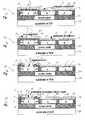
- any of the fully-depleted-collector SOI bipolar transistorscan be integrated with SOI CMOS devices to form SOI BiCMOS. This is due to the fact that the silicon layer thickness for fully-depleted-collector SOI bipolar transistors can be the same as the silicon thickness for high-speed SOI CMOS devices. For simplicity of illustration, only the process for integrating a vertical npn bipolar transistor structure shown in FIGS. 18 and 19 and CMOS devices is outlined here, in FIGS. 28 to 39 . The starting SOI wafer 30 , shown in FIG. 28, can be prepared by any one of the common SOI preparation processes.
- Isolation oxide 80can be formed by the usual masked oxidation of silicon, or by the usual shallow-trench isolation process which involves etching silicon trenches and then filling the trenches with oxide 80 followed by planarization using chemical-mechanical polishing. This is illustrated in FIG. 29.
- the depleted n-type collector region 16is formed by masked ion implantation.
- the n+ type reachthrough regions 22 of the bipolar transistorare formed by masked ion implantation.
- the regions 82 and 84 for the n-channel MOSFET and the p-channel MOSFET, respectively,are also doped by masked ion implantation.
- An insulator layer 86for example an oxide layer, is formed and patterned to insulate the bipolar transistor region.
- FIG. 30The gate insulators 87 and 88 for the CMOS devices are then formed, as shown in FIG. 31.
- a layer 90 of undoped polysiliconis deposited, as shown in FIG. 32. This polysilicon layer 90 serves to protect the gate insulators 87 and 88 while steps for forming the bipolar transistor are carried out.
- the polysilicon layer 90is doped heavily p-type where it is used as the base polysilicon contact layer 91 . This is illustrated in FIG. 33.
- the base window 92is etched open, as shown in FIG. 34
- a silicon layer 94is deposited epitaxially, forming single-crystalline silicon over the silicon in the base window 92 , and polycrystalline silicon over the polysilicon layer 90 and 91 .
- the single-crystalline part of this deposited silicon layer 94forms the base layer of the bipolar transistor.
- the polycrystalline partsimply adds to the thickness of the polysilicon layer 90 .
- This thickened polysilicon layer 90 and 94forms the base polysilicon contact layer for the bipolar transistor and the gate polysilicon layer for the CMOS devices. This is illustrated in FIG. 35.
- An insulator layer 96for example an oxide layer, is deposited, as shown in FIG. 36.
- the insulator layer 96 and polysilicon layers 90 and 94are then patterned by reactive-ion etching to form the polysilicon base contact structure.
- An oxide layeris deposited and then etched to form an oxide sidewall 98 to insulate the vertical polysilicon surfaces 91 , 94 and 90 , 94 .
- the emitter window 99is then etched open, and an n+ doped polysilicon layer 102 is deposited and patterned to form the polysilicon emitter.
- FIG. 37The gate polysilicon 90 , 94 for the CMOS devices are then patterned, and sidewall insulator 104 is formed on the vertical surface of the gate polysilicon.
- the gate polysilicon 90 , 94 , and the source regions 106 , 108 and drain regions 107 , 109 ,are then doped by ion implantation. This is illustrated in FIG. 38.
- Contacts 112 and 114 to the base and the collector respectively of the bipolar transistorare then etched open, as illustrated in FIG. 39.
- a top view of the bipolar transistoris similar to FIG. 19. This completes formation of the BiCMOS devices.
Landscapes
- Bipolar Transistors (AREA)
- Metal-Oxide And Bipolar Metal-Oxide Semiconductor Integrated Circuits (AREA)
Abstract
Description
- This invention relates to bipolar transistors and more particularly to a bipolar transistor structure suitable for implementation on silicon on insulator (SOI) alone or with Complementary Metal Oxide Semiconductor (CMOS) devices to provide SOI BiCMOS essential for most RF and communication products or digital products that have some critical analog components.[0001]
- High-performance bipolar transistors are vertical bipolar transistors, as opposed to lateral bipolar transistors. A vertical bipolar transistor, for example an npn[0002]
bipolar transistor 2 schematically shown in FIG. 1, comprises an n+type emitter region 3, a ptype base region 4, and an ntype collector region 5 stacked one on top of the other. In order to reduce collector series resistance, there is usually an n+type subcollector layer 6 beneath thecollector region 5 and an n+type reachthrough region 7 is used to bring the collector contact to the surface. - In normal operation, the emitter-base diode is forward biased, and the base-collector diode is reverse biased. The entire n type collector layer is usually thick enough to accommodate the space-charge region (also called the depletion region since it is normally depleted of mobile carriers) and a quasi-neutral region. The thickness, or width, of the space-charge region is determined by the collector doping concentration and the base-collector bias voltage. The quasi-neutral collector region can be very thin, usually just thick enough to prevent the space-charge region from reaching the n+ type subcollector layer. If the base-collector space-charge region touches the n+ type subcollector, it will cause the base-collector junction capacitance to increase and the base-collector junction breakdown voltage to decrease. The n+ type subcollector layer is usually rather thick, typically thicker than 1000 nm, in order to achieve an adequately small collector series resistance.[0003]
- In normal operation, electrons are injected from the emitter E and collected at the collector C. The dotted arrow shown in FIG. 2 indicates the electron path in normal operation, starting from the emitter contact. FIG. 3 is the energy-band diagram along the electron path. In FIGS. 2 and 3, A indicates the location of the emitter contact, A′ indicates the boundary between the depleted part and the quasi-neutral part of the n type collector, and A″ indicates the top of the n+ subcollector layer. In FIG. 3, the ordinate represents electron and hole energy.[0004]
- A more detailed description of the basic structure and operation of a bipolar transistor can be found in the book by Yuan Taur and Tak H. Ning entitled Fundamentals of Modern VLSI Devices,[0005]
Chapter 6, Bipolar Devices, Cambridge University Press, 1998, pp 292-347 which is incorporated herein by reference. - Vertical bipolar transistors have been built in the silicon layer of SOI. FIG. 4 illustrates a vertical npn[0006]
bipolar transistor 2′ using SOI. Usually, it is simply a vertical bipolar transistor, including its n+type subcollector layer 6, sitting on a buriedoxide layer 9 andsubstrate 8 of the SOI. The SOI silicon layer has to be rather thick, thick enough to accommodate the various layers of a vertical bipolar transistor described above. - SOI BiCMOS obtained from the integration of a vertical bipolar transistor with CMOS devices using SOI has been described in a publication by Toshiro Hiramoto, et al., “A 27 GHz double polysilicon bipolar technology on bonded SOI with embedded 58 μm[0007]2CMOS memory cells for ECL-CMOS SRAM applications,” IEDM Technical Digest, pp. 39-42, 1992.
- The thick silicon layer needed for the bipolar transistor results in the CMOS devices behaving like regular bulk CMOS devices, rather than like high-speed SOI CMOS devices. The silicon layer of high-speed SOI CMOS is usually rather thin, typically less than 200 nm, much too thin to accommodate present vertical bipolar transistor structures.[0008]
- It is possible to significantly reduce the silicon thickness needed for making SOI vertical[0009]
bipolar transistors 2″ by omitting the relatively thickn+ subcollector layer 6. This structure is illustrated in FIG. 5. The electrons still flows the same way as in a vertical bipolar transistor with a subcollector layer, namely vertically through the base layer and through the depletion layer of the base-collector diode to the quasi-neutral collector region. However, without then+ subcollector layer 6, electron current will have to be carried by the quasi-neutral collector layer which has very high sheet resistance because of its relatively light doping concentration and relatively small thickness compared to the n+type subcollector layer 6. The resulting collector series resistance is unacceptably large. If the n type collector thickness is increased significantly to reduce collector series resistance, the resultant SOI silicon layer will again be much to thick for integration with high-speed SOI CMOS devices. - In accordance with the present invention, a bipolar transistor on SOI is described comprising a substrate, an insulating layer over the substrate, a first single crystal semiconductor layer positioned over the insulating layer having a lightly doped region of a first type and at least one contiguous heavily doped region of the first type, the lightly doped region and the contiguous heavily doped region functioning as a collector, a second patterned semiconductor layer of a second type formed over the lightly doped region of the first semiconductor layer to function as the base, and a third patterned semiconductor layer of the first type positioned over the second semiconductor layer to function as the emitter, the lightly doped region of the first type of the collector having a dopant concentration to fully deplete of mobile charge through the first semiconductor layer to the insulating layer of the SOI below.[0010]
- The invention further provides an integrated circuit chip having both npn and pnp bipolar transistors of the above structure on SOI.[0011]
- The invention further provides an integrated circuit chip having one or both npn and pnp bipolar transistors of the above structure on SOI and p-channel MOSFETs and n-channel MOSFETs wherein the source and drain regions of the MOSFETs extend downward to the insulating layer of the SOI.[0012]
- The invention further provides a bipolar transistor on SOI comprising a substrate, an insulating layer over the substrate, a first single crystal semiconductor layer positioned over the insulating layer having a lightly doped region of a first type and at least one contiguous heavily doped region of the first type, the lightly doped region and the contiguous heavily doped region functioning as a collector, a top region of the lightly doped region is counter-doped to a second type to function as the base, a second patterned semiconductor layer of the second type formed over a region of the counter-doped region of the first semiconductor layer to function as the extrinsic base, and a third patterned semiconductor layer of the first type positioned over the counter-doped region of the first semiconductor layer to function as the emitter, the lightly doped region of the first type in the first semiconductor layer having a dopant concentration to fully deplete of mobile charge through the first semiconductor layer to the insulating layer of the SOI below.[0013]
- The invention further provides an integrated circuit chip having both npn and pnp bipolar transistors of the above structure on SOI.[0014]
- The invention further provides an integrated circuit chip having one or both npn and pnp bipolar transistors of the above structure on SOI and p-channel MOSFETs and n-channel MOSFETs wherein the source and drain regions of the MOSFETs extend downward to the insulating layer of the SOI.[0015]
- The invention provides a fully-depleted-collector SOI vertical bipolar transistor which has a much smaller base-collector junction capacitance than conventional devices and does not require a heavily doped subcollector layer.[0016]
- The invention provides an SOI bipolar transistor structure which uses thin-silicon SOI typically less than 200 nm, and is therefore readily compatible with high-speed SOI CMOS devices also using thin-silicon SOI for making high-speed SOI BiCMOS.[0017]
- These and other features, objects, and advantages of the present invention will become apparent upon consideration of the following detailed description of the invention when read in conjunction with the drawing in which:[0018]
- FIG. 1 is a cross section schematic view of a vertical bipolar transistor of the prior art.[0019]
- FIG. 2 is a cross section schematic view of a vertical bipolar transistor of the prior art with the electron path shown through the transistor.[0020]
- FIG. 3 is a graph of the energy-band diagram along the electron current path shown in FIG. 2.[0021]
- FIG. 4 is a cross section schematic view of a vertical npn bipolar transistor using SOI of the prior art.[0022]
- FIG. 5 is a cross section schematic view of an alternate vertical npn bipolar transistor structure on SOI illustrating deficiencies due to the high series resistance through the collector.[0023]
- FIG. 6 is a cross section schematic view of one embodiment of the invention.[0024]
- FIG. 7 is a cross section schematic view of the electron current path through the embodiment of FIG. 6.[0025]
- FIG. 8 shows an energy band diagram along the electron current path shown in FIG. 7.[0026]
- FIGS.[0027]9-18 are cross section schematic views illustrating the steps for fabricating a fully-depleted-collector SOI vertical npn bipolar transistor having the base region formed in an epitaxially deposited silicon layer.
- FIG. 18 is a cross section view along the lines[0028]18-18 of FIG. 19.
- FIG. 19 is a top schematic view of the transistor shown in FIG. 18.[0029]
- FIGS.[0030]20-27 are cross section schematic views illustrating the steps for fabricating a double-polysilicon self-aligned vertical npn bipolar transistor.
- FIGS.[0031]28-39 are cross section schematic views illustrating the steps for fabricating a vertical npn bipolar transistor structure shown in FIG. 18 and CMOS devices to provide SOI BiCMOS.
- The basic structure of the fully-depleted-collector SOI npn[0032]
bipolar transistor 10 is illustrated in FIG. 6.Bipolar transistor 10 has anemitter 12 of n+ type semiconductor, abase 14 of p type semiconductor and acollector 16 having a depletedn collector region 18 and a quasi-neutraln collector region 20. An n+type semiconductor region 22 contiguous with quasi-neutraln collector region 20 provides a low impedance reachthrough for electrical connection to circuit wiring. As shown in FIG. 6,emitter 12 is overbase 14.Base 14 is overcollector region 18 and does not contactcollector region 20.Collector region 20 is positioned betweencollector region 18 and n+ type semiconductor region orreachthrough 22.Collector regions type semiconductor region 22 are positioned over buriedoxide layer 26. Below buriedoxide layer 26 is oversubstrate 28. Silicon-on-Insulator 30 comprisessemiconductor regions oxide 26 andsubstrate 28. Electrical contact tobipolar transistor 10 may be made via contact to leads32,34 and36 which are coupled, respectively, to theemitter 12,base 14 andcollector 16 viasemiconductor region 22. - FIG. 6 shows that there is no[0033]
quasi-neutral collector region 18 underneath thebase region 14. Thecollector region 18 directly underneathbase 14 is fully depleted. There is only a space-charge region between thebase region 14 and the buriedoxide layer 26 ofSOI 30. There is a smallquasi-neutral collector region 20 horizontally between the fully-depleted collector region18 (the space-charge region) and thecollector reachthrough region 22. There is no need for an n+ type subcollector layer as used in the prior art. The n+ type reachthrough22, thequasi-neutral collector region 20, and the fully-depletedcollector region 18 all lie on top of the buriedoxide 26 of theSOI 30. - The electron current path for this fully-depleted-collector SOI[0034]
bipolar transistor 10 is indicated in FIG. 7 byarrow 40. Electrons from theemitter 12 enter the space-charge region 18 of thecollector 16 after traversing thebase 14. Once inside the space-charge region 18, these electrons follow the electric field in the space-charge region and drift more or less laterally towards thequasi-neutral region 20 ofcollector 16. From there, electron current is carried by the n+ type reachthrough22 to the semiconductor surface. Since the electrons traverse the space-charge region 18 more or less laterally, instead of vertically in a traditional vertical bipolar transistor as shown in FIG. 2, there is no need for an n+ type subcollector layer. The energy-band diagram along theelectron path 40 is illustrated in FIG. 8. Position A indicates theemitter contact 32. Position A′ indicates where the electrons approach the buriedoxide 26 of theSOI 30. Position A″ indicates where the electrons reach thequasi-neutral region 20 ofcollector 16. - For the traditional vertical bipolar transistor, such as the one shown in FIGS. 1, 4, or[0035]5, the base-collector junction capacitance is given by the usual base-collector diode space-charge layer capacitor. For the fully-depleted-collector SOI
bipolar transistor 10, the base-collector junction capacitance is given by two capacitors in series. They are the vertical space-charge layer capacitor and the buried oxide capacitor. For two capacitors in series, the combined capacitance is determined primarily by the smaller of the two capacitors. Thus, the base-collector junction capacitance of the fully-depleted-collector SOI transistor is determined primarily by the buried oxide capacitor. This capacitance is much smaller than the base-collector junction capacitance of a traditional vertical bipolar transistor. - As an example, consider a vertical bipolar transistor with a collector doping concentration of 2×10[0036]17cm−3and a base-collector reverse bias of 3 V. The base-collector diode space-charge width is about 160 nm. This width is about the same as the thickness of the silicon layer of high-speed SOI CMOS devices. Thus the fully-depleted-collector
bipolar transistor 10 is readily compatible with high-speed SOI CMOS for making high-speed SOI BiCMOS. - The fully-depleted-collector SOI[0037]
bipolar transistor 10 can be implemented with the commonly used vertical bipolar structures and processes. Thus, it can be of the double-polysilicon self-aligned type, or double-polysilicon non-self-aligned type. The intrinsic base layer can be formed by epitaxial deposition of silicon or by ion implantation of the silicon layer overinsulator 26 ofSOI 30. With epitaxially deposited silicon for thebase 14, germanium can also be added during deposition to form a SiGe-basebipolar transistor 10. - A process for fabricating a fully-depleted-collector SOI[0038]
bipolar transistor 10, using a double-polysilicon non-self-aligned structure and epitaxial deposition of silicon, or silicon-germanium (SiGe) alloy, for forming the intrinsic base is outlined in FIGS.9 to18. The startingSOI wafer 30 shown in FIG. 9, can be prepared by any one of the common SOI preparation processes. Isolation oxide can be formed by the usual masked oxidation of silicon, or by the usual shallow-trench isolation processes which involve etching silicon trenches and then filling the trenches with oxide followed by planarization using chemical-mechanical polishing. The resulting structure is illustrated in FIG. 10. A blanket implantation step is then made to dope the n-type collector region 16. The implantation step provides a concentration so that the n-type collector region 16 will be completely depleted when the transistor is used in circuit applications. For example, if the silicon layer thickness is 100 nm and the base-collector diode is reverse-biased at 3 V, full depletion of the collector region is assured if its average doping concentration is less than about 3×1017cm−3. A masked implantation step is used to dope thereachthrough region 22, which is shown as surrounding thecollector region 16, more heavily. This is illustrated in FIG. 11. Aninsulator layer 50, for example an oxide layer, is deposited or formed. A heavily p-type dopedpolysilicon layer 52, which will form part of the base contact polysilicon layer, is deposited. This is illustrated in FIG. 12. The base region window is etched open, as shown in FIG. 13. A layer ofsilicon 54 is then grown or deposited epitaxially overcollector 16. Over the single-crystal base window region, the depositedsilicon layer 54 is crystalline and forms the intrinsic base of the bipolar transistor, but over thepolysilicon region 52, the depositedsilicon layer 54 is polycrystalline and simply adds to the thickness ofpolysilicon layer 52. The intrinsic base is doped p-type. The doping can be done by boron implantation of the deposited layer ofsilicon 54, or by in situ doping ofsilicon layer 54 during deposition. If germanium is added tosilicon layer 54 during deposition, the resulting transistor will be a SiGe-base bipolar transistor. A layer ofinsulator 56, for example an oxide layer, is then deposited. This is shown in FIG. 14. Thebase polysilicon layer 54 is patterned, followed by an oxide deposition and reactive-ion etching to form asidewall oxide 57 on the vertical surface of the etchedpolysilicon 54, as shown in FIG. 15. The emitter window is etched open, as shown in FIG. 16. Ann+ polysilicon emitter 58 is formed as shown in FIG. 17. Contact windows to the base and the collector are then etched open. The cross section view of a completed transistor is shown in FIG. 18. A top schematic view of the completed transistor is shown in FIG. 19. - A process for fabricating a double-polysilicon self-aligned bipolar transistor, using ion-implantation for forming the intrinsic base region, is outlined in FIGS.[0039]20 to27. The starting
SOI wafer 30 shown in FIG. 20, can be prepared by any of the common SOI preparation process. Isolation oxide can be formed by the usual masked oxidation of silicon process, or by the usual shallow-trench isolation processes which involve etching silicon trenches and then filling the trenches with oxide followed by planarization using chemical-mechanical polishing. This is illustrated in FIG. 21. A blanket implantation step is then made to dope the n-type collector region 16. The implantation step provides a concentration so that the n-type collector region 16 will be completed depleted when the transistor is used in circuit applications. A masked implantation step is used to dope more heavily thereachthrough region 22, which is shown as surrounding thecollector region 16. This is illustrated in FIG. 22. An insulator layer, for example anoxide layer 60, is deposited or formed. The base window is etched open. This is illustrated in FIG. 23. A heavily p-type polysilicon layer62 is deposited. Polysilicon layer62 forms the base polysilicon contact layer. It can be doped in situ during deposition, or doped by ion implantation of an undoped polysilicon layer. Aninsulator layer 64, for example an oxide layer, is then deposited or formed. This is illustrated in FIG. 24. The base polysilicon layer62 is patterned and asidewall insulator layer 66 is formed on the vertical etched surface. A thermal annealing process is carried out to drive the p-type dopant from the polysilicon layer62 into the single crystal region to formp+ regions p+ regions intrinsic base region 70 is formed by boron implantation. Then+ polysilicon emitter 72 is then formed. This is illustrated in FIG. 26. Thebase contact 74 and thecollector contact 76 are then etched open. This completes formation of the double-polysilicon self-aligned implanted-base fully-depleted-collector SOIbipolar transistor 72, shown in FIG. 27. - It should be noted that fully-depleted-collector SOI pnp bipolar transistors can also be made by following the processes outlined in FIGS.[0040]9 to19 and in FIGS.20 to27 but using dopant impurities of the opposite type. Furthermore, both vertical npn and pnp bipolar transistors can be made on the same silicon layer of the
SOI 30 for use in complementary bipolar circuits. - Any of the fully-depleted-collector SOI bipolar transistors can be integrated with SOI CMOS devices to form SOI BiCMOS. This is due to the fact that the silicon layer thickness for fully-depleted-collector SOI bipolar transistors can be the same as the silicon thickness for high-speed SOI CMOS devices. For simplicity of illustration, only the process for integrating a vertical npn bipolar transistor structure shown in FIGS. 18 and 19 and CMOS devices is outlined here, in FIGS.[0041]28 to39. The starting
SOI wafer 30, shown in FIG. 28, can be prepared by any one of the common SOI preparation processes.Isolation oxide 80 can be formed by the usual masked oxidation of silicon, or by the usual shallow-trench isolation process which involves etching silicon trenches and then filling the trenches withoxide 80 followed by planarization using chemical-mechanical polishing. This is illustrated in FIG. 29. The depleted n-type collector region 16 is formed by masked ion implantation. The n+ typereachthrough regions 22 of the bipolar transistor are formed by masked ion implantation. Theregions insulator layer 86, for example an oxide layer, is formed and patterned to insulate the bipolar transistor region. This is illustrated in FIG. 30. The gate insulators87 and88 for the CMOS devices are then formed, as shown in FIG. 31. Alayer 90 of undoped polysilicon is deposited, as shown in FIG. 32. Thispolysilicon layer 90 serves to protect thegate insulators polysilicon layer 90 is doped heavily p-type where it is used as the basepolysilicon contact layer 91. This is illustrated in FIG. 33. Thebase window 92 is etched open, as shown in FIG. 34 Asilicon layer 94 is deposited epitaxially, forming single-crystalline silicon over the silicon in thebase window 92, and polycrystalline silicon over thepolysilicon layer silicon layer 94 forms the base layer of the bipolar transistor. The polycrystalline part simply adds to the thickness of thepolysilicon layer 90. This thickenedpolysilicon layer insulator layer 96, for example an oxide layer, is deposited, as shown in FIG. 36. Theinsulator layer 96 andpolysilicon layers oxide sidewall 98 to insulate the vertical polysilicon surfaces91,94 and90,94. The emitter window99 is then etched open, and an n+ doped polysilicon layer102 is deposited and patterned to form the polysilicon emitter. This is illustrated in FIG. 37. Thegate polysilicon sidewall insulator 104 is formed on the vertical surface of the gate polysilicon. Thegate polysilicon source regions 106,108 anddrain regions Contacts 112 and114 to the base and the collector respectively of the bipolar transistor are then etched open, as illustrated in FIG. 39. A top view of the bipolar transistor is similar to FIG. 19. This completes formation of the BiCMOS devices. - It should be noted that in the drawing like elements or components are referred to by like and corresponding reference numerals.[0042]
- While there has been described and illustrated a bipolar transistor structure having a fully depleted collector region on an insulator and without the need for an n+ subcollector, it will be apparent to those skilled in the art that modifications and variations are possible without deviating from the broad scope of the invention which shall be limited solely by the scope of the claims appended hereto.[0043]
Claims (22)
Priority Applications (6)
| Application Number | Priority Date | Filing Date | Title |
|---|---|---|---|
| US09/757,965US6849871B2 (en) | 2000-10-20 | 2001-01-10 | Fully-depleted-collector silicon-on-insulator (SOI) bipolar transistor useful alone or in SOI BiCMOS |
| SG200105829ASG100757A1 (en) | 2000-10-20 | 2001-09-25 | Fully-depleted-collector silicon-on-insulator (soi) bipolar transistor useful alone or in soi bicmos |
| TW090125680ATW538509B (en) | 2000-10-20 | 2001-10-17 | Fully-depleted-collector Silicon-on-Insulator (SOI) bipolar transistor useful alone or in SOI BiCMOS |
| KR10-2001-0064169AKR100413751B1 (en) | 2000-10-20 | 2001-10-18 | FULLY-DEPLETED-COLLECTOR SILICON-ON-INSULATOR(SOI) BIPOLAR TRANSISTOR USEFUL ALONE OR IN SOI BiCMOS |
| CNB01137022XACN1205672C (en) | 2000-10-20 | 2001-10-19 | Fully Depleted Collector Si-Insulator Bipolar Transistor |
| US10/993,244US6949764B2 (en) | 2000-10-20 | 2004-11-19 | Fully-depleted-collector silicon-on-insulator (SOI) bipolar transistor useful alone or in SOI BiCMOS |
Applications Claiming Priority (2)
| Application Number | Priority Date | Filing Date | Title |
|---|---|---|---|
| US24233900P | 2000-10-20 | 2000-10-20 | |
| US09/757,965US6849871B2 (en) | 2000-10-20 | 2001-01-10 | Fully-depleted-collector silicon-on-insulator (SOI) bipolar transistor useful alone or in SOI BiCMOS |
Related Child Applications (1)
| Application Number | Title | Priority Date | Filing Date |
|---|---|---|---|
| US10/993,244DivisionUS6949764B2 (en) | 2000-10-20 | 2004-11-19 | Fully-depleted-collector silicon-on-insulator (SOI) bipolar transistor useful alone or in SOI BiCMOS |
Publications (2)
| Publication Number | Publication Date |
|---|---|
| US20020089038A1true US20020089038A1 (en) | 2002-07-11 |
| US6849871B2 US6849871B2 (en) | 2005-02-01 |
Family
ID=26935015
Family Applications (2)
| Application Number | Title | Priority Date | Filing Date |
|---|---|---|---|
| US09/757,965Expired - LifetimeUS6849871B2 (en) | 2000-10-20 | 2001-01-10 | Fully-depleted-collector silicon-on-insulator (SOI) bipolar transistor useful alone or in SOI BiCMOS |
| US10/993,244Expired - LifetimeUS6949764B2 (en) | 2000-10-20 | 2004-11-19 | Fully-depleted-collector silicon-on-insulator (SOI) bipolar transistor useful alone or in SOI BiCMOS |
Family Applications After (1)
| Application Number | Title | Priority Date | Filing Date |
|---|---|---|---|
| US10/993,244Expired - LifetimeUS6949764B2 (en) | 2000-10-20 | 2004-11-19 | Fully-depleted-collector silicon-on-insulator (SOI) bipolar transistor useful alone or in SOI BiCMOS |
Country Status (5)
| Country | Link |
|---|---|
| US (2) | US6849871B2 (en) |
| KR (1) | KR100413751B1 (en) |
| CN (1) | CN1205672C (en) |
| SG (1) | SG100757A1 (en) |
| TW (1) | TW538509B (en) |
Cited By (70)
| Publication number | Priority date | Publication date | Assignee | Title |
|---|---|---|---|---|
| US20040124488A1 (en)* | 2001-06-18 | 2004-07-01 | Pierre Fazan | Semiconductor device |
| US20040228168A1 (en)* | 2003-05-13 | 2004-11-18 | Richard Ferrant | Semiconductor memory device and method of operating same |
| US20040227166A1 (en)* | 2003-05-13 | 2004-11-18 | Lionel Portmann | Reference current generator, and method of programming, adjusting and/or operating same |
| US20040240306A1 (en)* | 2002-04-18 | 2004-12-02 | Pierre Fazan | Data storage device and refreshing method for use with such device |
| US20040238890A1 (en)* | 2002-04-18 | 2004-12-02 | Pierre Fazan | Semiconductor device |
| US20050013163A1 (en)* | 2003-05-13 | 2005-01-20 | Richard Ferrant | Semiconductor memory cell, array, architecture and device, and method of operating same |
| US20050017240A1 (en)* | 2003-07-22 | 2005-01-27 | Pierre Fazan | Integrated circuit device, and method of fabricating same |
| US20050063224A1 (en)* | 2003-09-24 | 2005-03-24 | Pierre Fazan | Low power programming technique for a floating body memory transistor, memory cell, and memory array |
| US20050164454A1 (en)* | 2004-01-27 | 2005-07-28 | Micron Technology, Inc. | Selective epitaxy vertical integrated circuit components and methods |
| US20060091462A1 (en)* | 2004-11-04 | 2006-05-04 | Serguei Okhonin | Memory cell having an electrically floating body transistor and programming technique therefor |
| US20060098481A1 (en)* | 2004-11-10 | 2006-05-11 | Serguei Okhonin | Circuitry for and method of improving statistical distribution of integrated circuits |
| US20060126374A1 (en)* | 2004-12-13 | 2006-06-15 | Waller William K | Sense amplifier circuitry and architecture to write data into and/or read from memory cells |
| US20060131650A1 (en)* | 2004-12-22 | 2006-06-22 | Serguei Okhonin | Bipolar reading technique for a memory cell having an electrically floating body transistor |
| US20070023833A1 (en)* | 2005-07-28 | 2007-02-01 | Serguei Okhonin | Method for reading a memory cell having an electrically floating body transistor, and memory cell and array implementing same |
| US20070058427A1 (en)* | 2005-09-07 | 2007-03-15 | Serguei Okhonin | Memory cell and memory cell array having an electrically floating body transistor, and methods of operating same |
| US20070064489A1 (en)* | 2005-09-19 | 2007-03-22 | Philippe Bauser | Method and circuitry to generate a reference current for reading a memory cell, and device implementing same |
| US20070085140A1 (en)* | 2005-10-19 | 2007-04-19 | Cedric Bassin | One transistor memory cell having strained electrically floating body region, and method of operating same |
| US20070138530A1 (en)* | 2005-12-19 | 2007-06-21 | Serguei Okhonin | Electrically floating body memory cell and array, and method of operating or controlling same |
| US20070187775A1 (en)* | 2006-02-16 | 2007-08-16 | Serguei Okhonin | Multi-bit memory cell having electrically floating body transistor, and method of programming and reading same |
| US20070285982A1 (en)* | 2006-04-07 | 2007-12-13 | Eric Carman | Memory array having a programmable word length, and method of operating same |
| US7368765B1 (en)* | 2005-12-20 | 2008-05-06 | Hrl Laboratories, Llc | Bipolar transistors with low parasitic losses |
| US7372084B1 (en)* | 2005-12-20 | 2008-05-13 | Hrl Laboratories, Llc | Low power bipolar transistors with low parasitic losses |
| US7542340B2 (en) | 2006-07-11 | 2009-06-02 | Innovative Silicon Isi Sa | Integrated circuit including memory array having a segmented bit line architecture and method of controlling and/or operating same |
| US7606098B2 (en) | 2006-04-18 | 2009-10-20 | Innovative Silicon Isi Sa | Semiconductor memory array architecture with grouped memory cells, and method of controlling same |
| US7863133B2 (en) | 2005-06-28 | 2011-01-04 | Micron Technology, Inc. | Oxide epitaxial isolation |
| US7924630B2 (en) | 2008-10-15 | 2011-04-12 | Micron Technology, Inc. | Techniques for simultaneously driving a plurality of source lines |
| US7933142B2 (en) | 2006-05-02 | 2011-04-26 | Micron Technology, Inc. | Semiconductor memory cell and array using punch-through to program and read same |
| US7933140B2 (en) | 2008-10-02 | 2011-04-26 | Micron Technology, Inc. | Techniques for reducing a voltage swing |
| US7947543B2 (en) | 2008-09-25 | 2011-05-24 | Micron Technology, Inc. | Recessed gate silicon-on-insulator floating body device with self-aligned lateral isolation |
| US20110122687A1 (en)* | 2009-11-24 | 2011-05-26 | Innovative Silicon Isi Sa | Techniques for reducing disturbance in a semiconductor device |
| US7957206B2 (en) | 2008-04-04 | 2011-06-07 | Micron Technology, Inc. | Read circuitry for an integrated circuit having memory cells and/or a memory cell array, and method of operating same |
| US8014195B2 (en) | 2008-02-06 | 2011-09-06 | Micron Technology, Inc. | Single transistor memory cell |
| US8064274B2 (en) | 2007-05-30 | 2011-11-22 | Micron Technology, Inc. | Integrated circuit having voltage generation circuitry for memory cell array, and method of operating and/or controlling same |
| US8069377B2 (en) | 2006-06-26 | 2011-11-29 | Micron Technology, Inc. | Integrated circuit having memory array including ECC and column redundancy and method of operating the same |
| US8085594B2 (en) | 2007-06-01 | 2011-12-27 | Micron Technology, Inc. | Reading technique for memory cell with electrically floating body transistor |
| US8139418B2 (en) | 2009-04-27 | 2012-03-20 | Micron Technology, Inc. | Techniques for controlling a direct injection semiconductor memory device |
| US8189376B2 (en) | 2008-02-08 | 2012-05-29 | Micron Technology, Inc. | Integrated circuit having memory cells including gate material having high work function, and method of manufacturing same |
| US8194487B2 (en) | 2007-09-17 | 2012-06-05 | Micron Technology, Inc. | Refreshing data of memory cells with electrically floating body transistors |
| US8199595B2 (en) | 2009-09-04 | 2012-06-12 | Micron Technology, Inc. | Techniques for sensing a semiconductor memory device |
| US8213226B2 (en) | 2008-12-05 | 2012-07-03 | Micron Technology, Inc. | Vertical transistor memory cell and array |
| US8223574B2 (en) | 2008-11-05 | 2012-07-17 | Micron Technology, Inc. | Techniques for block refreshing a semiconductor memory device |
| US8264041B2 (en) | 2007-01-26 | 2012-09-11 | Micron Technology, Inc. | Semiconductor device with electrically floating body |
| US8310893B2 (en) | 2009-12-16 | 2012-11-13 | Micron Technology, Inc. | Techniques for reducing impact of array disturbs in a semiconductor memory device |
| US8315099B2 (en) | 2009-07-27 | 2012-11-20 | Micron Technology, Inc. | Techniques for providing a direct injection semiconductor memory device |
| US8319294B2 (en) | 2009-02-18 | 2012-11-27 | Micron Technology, Inc. | Techniques for providing a source line plane |
| CN102800590A (en)* | 2012-08-24 | 2012-11-28 | 中国科学院上海微系统与信息技术研究所 | Preparation method of SOI (silicon on insulator)-based SiGe-HBT (heterojunction bipolar transistor) |
| CN102800589A (en)* | 2012-08-24 | 2012-11-28 | 中国科学院上海微系统与信息技术研究所 | Preparation method of SOI (silicon on insulator)-based SiGe-HBT (heterojunction bipolar transistor) |
| US8349662B2 (en) | 2007-12-11 | 2013-01-08 | Micron Technology, Inc. | Integrated circuit having memory cell array, and method of manufacturing same |
| US8369177B2 (en) | 2010-03-05 | 2013-02-05 | Micron Technology, Inc. | Techniques for reading from and/or writing to a semiconductor memory device |
| US8411513B2 (en) | 2010-03-04 | 2013-04-02 | Micron Technology, Inc. | Techniques for providing a semiconductor memory device having hierarchical bit lines |
| US8411524B2 (en) | 2010-05-06 | 2013-04-02 | Micron Technology, Inc. | Techniques for refreshing a semiconductor memory device |
| US8416636B2 (en) | 2010-02-12 | 2013-04-09 | Micron Technology, Inc. | Techniques for controlling a semiconductor memory device |
| US8498157B2 (en) | 2009-05-22 | 2013-07-30 | Micron Technology, Inc. | Techniques for providing a direct injection semiconductor memory device |
| US8508994B2 (en) | 2009-04-30 | 2013-08-13 | Micron Technology, Inc. | Semiconductor device with floating gate and electrically floating body |
| US8518774B2 (en) | 2007-03-29 | 2013-08-27 | Micron Technology, Inc. | Manufacturing process for zero-capacitor random access memory circuits |
| US8531878B2 (en) | 2011-05-17 | 2013-09-10 | Micron Technology, Inc. | Techniques for providing a semiconductor memory device |
| US8537610B2 (en) | 2009-07-10 | 2013-09-17 | Micron Technology, Inc. | Techniques for providing a semiconductor memory device |
| US8536628B2 (en) | 2007-11-29 | 2013-09-17 | Micron Technology, Inc. | Integrated circuit having memory cell array including barriers, and method of manufacturing same |
| US8547738B2 (en) | 2010-03-15 | 2013-10-01 | Micron Technology, Inc. | Techniques for providing a semiconductor memory device |
| US8576631B2 (en) | 2010-03-04 | 2013-11-05 | Micron Technology, Inc. | Techniques for sensing a semiconductor memory device |
| US8710566B2 (en) | 2009-03-04 | 2014-04-29 | Micron Technology, Inc. | Techniques for forming a contact to a buried diffusion layer in a semiconductor memory device |
| US8748959B2 (en) | 2009-03-31 | 2014-06-10 | Micron Technology, Inc. | Semiconductor memory device |
| US8773933B2 (en) | 2012-03-16 | 2014-07-08 | Micron Technology, Inc. | Techniques for accessing memory cells |
| FR3000842A1 (en)* | 2013-01-08 | 2014-07-11 | St Microelectronics Rousset | TRANSISTOR FOR SELECTING A MEMORY CELL |
| US20140353726A1 (en)* | 2013-05-29 | 2014-12-04 | International Business Machines Corporation | Lateral bipolar transistors having partially-depleted intrinsic base |
| US9559216B2 (en) | 2011-06-06 | 2017-01-31 | Micron Technology, Inc. | Semiconductor memory device and method for biasing same |
| US20170301755A1 (en)* | 2016-04-13 | 2017-10-19 | International Business Machines Corporation | Lateral bipolar junction transistor with abrupt junction and compound buried oxide |
| US10825921B2 (en) | 2016-07-15 | 2020-11-03 | International Business Machines Corporation | Lateral bipolar junction transistor with controlled junction |
| CN113206108A (en)* | 2020-05-28 | 2021-08-03 | 台湾积体电路制造股份有限公司 | Semiconductor-on-insulator substrate, semiconductor structure and forming method thereof |
| CN113454769A (en)* | 2018-12-24 | 2021-09-28 | Soitec公司 | Semiconductor structure for digital and radio frequency applications and process for manufacturing such a structure |
Families Citing this family (52)
| Publication number | Priority date | Publication date | Assignee | Title |
|---|---|---|---|---|
| US7825488B2 (en)* | 2006-05-31 | 2010-11-02 | Advanced Analogic Technologies, Inc. | Isolation structures for integrated circuits and modular methods of forming the same |
| US7902630B2 (en)* | 2002-08-14 | 2011-03-08 | Advanced Analogic Technologies, Inc. | Isolated bipolar transistor |
| US7834421B2 (en)* | 2002-08-14 | 2010-11-16 | Advanced Analogic Technologies, Inc. | Isolated diode |
| US20080197408A1 (en)* | 2002-08-14 | 2008-08-21 | Advanced Analogic Technologies, Inc. | Isolated quasi-vertical DMOS transistor |
| US8513087B2 (en)* | 2002-08-14 | 2013-08-20 | Advanced Analogic Technologies, Incorporated | Processes for forming isolation structures for integrated circuit devices |
| US7956391B2 (en)* | 2002-08-14 | 2011-06-07 | Advanced Analogic Technologies, Inc. | Isolated junction field-effect transistor |
| US7939420B2 (en)* | 2002-08-14 | 2011-05-10 | Advanced Analogic Technologies, Inc. | Processes for forming isolation structures for integrated circuit devices |
| US7667268B2 (en)* | 2002-08-14 | 2010-02-23 | Advanced Analogic Technologies, Inc. | Isolated transistor |
| US8089129B2 (en)* | 2002-08-14 | 2012-01-03 | Advanced Analogic Technologies, Inc. | Isolated CMOS transistors |
| US20040222485A1 (en)* | 2002-12-17 | 2004-11-11 | Haynie Sheldon D. | Bladed silicon-on-insulator semiconductor devices and method of making |
| FR2854494A1 (en)* | 2003-05-02 | 2004-11-05 | St Microelectronics Sa | METHOD FOR MANUFACTURING A BIPOLAR TRANSISTOR |
| KR100586737B1 (en) | 2003-12-26 | 2006-06-08 | 한국전자통신연구원 | NMOS devices, PMOS devices and SiSiWOCMOS devices implemented on a SOI substrate, and methods of manufacturing the same |
| KR100752182B1 (en)* | 2005-10-12 | 2007-08-24 | 동부일렉트로닉스 주식회사 | CMOS image sensor and its manufacturing method |
| KR100833491B1 (en)* | 2005-12-08 | 2008-05-29 | 한국전자통신연구원 | Embedded phase-change memory and method of fabrication the same |
| US7772060B2 (en)* | 2006-06-21 | 2010-08-10 | Texas Instruments Deutschland Gmbh | Integrated SiGe NMOS and PMOS transistors |
| US20080001234A1 (en)* | 2006-06-30 | 2008-01-03 | Kangguo Cheng | Hybrid Field Effect Transistor and Bipolar Junction Transistor Structures and Methods for Fabricating Such Structures |
| US8030731B2 (en)* | 2007-03-28 | 2011-10-04 | Advanced Analogic Technologies, Inc. | Isolated rectifier diode |
| CN101719508B (en)* | 2009-11-10 | 2013-09-04 | 上海宏力半导体制造有限公司 | Thin SOI longitudinal bipolar transistor and manufacturing method thereof |
| CN102104063B (en)* | 2009-12-17 | 2012-10-31 | 中国科学院上海微系统与信息技术研究所 | A kind of SOI vertical bipolar transistor and its manufacturing method |
| CN102412274B (en)* | 2011-01-13 | 2014-02-26 | 上海华虹宏力半导体制造有限公司 | Vertical parasitic PNP device and manufacturing method in silicon germanium HBT process |
| US8441084B2 (en)* | 2011-03-15 | 2013-05-14 | International Business Machines Corporation | Horizontal polysilicon-germanium heterojunction bipolar transistor |
| US8492794B2 (en) | 2011-03-15 | 2013-07-23 | International Business Machines Corporation | Vertical polysilicon-germanium heterojunction bipolar transistor |
| US9379257B2 (en)* | 2012-06-22 | 2016-06-28 | Infineon Technologies Ag | Electrical device and method for manufacturing same |
| CN102751293B (en)* | 2012-07-16 | 2016-01-20 | 西安电子科技大学 | A kind of SOI tri-strains plane BiCMOS integrated device and preparation method |
| CN102916015B (en)* | 2012-07-16 | 2014-12-31 | 西安电子科技大学 | Strain Si BiCMOS (Bipolar Complementary Metal Oxide Semiconductor) integrated device based on SOI SiGe HBT (Heterojunction Bipolar Transistor) and preparation method thereof |
| CN102751290B (en)* | 2012-07-16 | 2015-12-02 | 西安电子科技大学 | A kind of three polycrystalline mixing crystal face strain BiCMOS integrated device and preparation methods |
| CN102916041B (en)* | 2012-11-15 | 2015-03-25 | 中国科学院上海微系统与信息技术研究所 | Germanium-silicon heterojunction bipolar transistor based on SOI (Silicon On Insulator) and manufacturing method thereof |
| US9922866B2 (en) | 2015-07-31 | 2018-03-20 | International Business Machines Corporation | Enhancing robustness of SOI substrate containing a buried N+ silicon layer for CMOS processing |
| US9859172B1 (en) | 2016-09-29 | 2018-01-02 | International Business Machines Corporation | Bipolar transistor compatible with vertical FET fabrication |
| US10014397B1 (en) | 2016-12-19 | 2018-07-03 | Globalfoundries Inc. | Bipolar junction transistors with a combined vertical-lateral architecture |
| CN106876271A (en)* | 2017-02-10 | 2017-06-20 | 江苏能华微电子科技发展有限公司 | The preparation method of gallium nitride power triode |
| US10367084B2 (en) | 2017-07-31 | 2019-07-30 | Globalfoundries Inc. | Cascode heterojunction bipolar transistors |
| US10332972B2 (en)* | 2017-11-20 | 2019-06-25 | International Business Machines Corporation | Single column compound semiconductor bipolar junction transistor fabricated on III-V compound semiconductor surface |
| US11189701B1 (en)* | 2020-12-11 | 2021-11-30 | International Business Machines Corporation | Bipolar junction transistor with vertically integrated resistor |
| US11637181B2 (en) | 2021-08-20 | 2023-04-25 | Globalfoundries U.S. Inc. | Lateral bipolar transistors with polysilicon terminals |
| US11799021B2 (en) | 2021-08-23 | 2023-10-24 | Globalfoundries U.S. Inc. | Lateral bipolar transistor structure with marker layer for emitter and collector |
| US12040388B2 (en) | 2021-08-25 | 2024-07-16 | Globalfoundries U.S. Inc. | Lateral bipolar transistors |
| US11990535B2 (en) | 2021-08-25 | 2024-05-21 | Globalfoundries U.S. Inc. | Lateral heterojunction bipolar transistor with emitter and/or collector regrown from substrate and method |
| US11784224B2 (en) | 2021-08-26 | 2023-10-10 | Globalfoundries U.S. Inc. | Lateral bipolar transistor structure with base over semiconductor buffer and related method |
| US11949004B2 (en) | 2021-08-27 | 2024-04-02 | Globalfoundries U.S. Inc. | Lateral bipolar transistors with gate structure aligned to extrinsic base |
| US11888050B2 (en) | 2021-08-27 | 2024-01-30 | Globalfoundries U.S. Inc. | Lateral bipolar transistor structure with inner and outer spacers and methods to form same |
| US11888031B2 (en) | 2021-08-27 | 2024-01-30 | Globalfoundries U.S. Inc. | Fin-based lateral bipolar junction transistor and method |
| US11710771B2 (en) | 2021-09-01 | 2023-07-25 | Globalfoundries U.S. Inc. | Non-self-aligned lateral bipolar junction transistors |
| US11908898B2 (en) | 2021-09-02 | 2024-02-20 | Globalfoundries U.S. Inc. | Lateral bipolar transistor structure with base layer of varying horizontal width and methods to form same |
| US11769806B2 (en) | 2021-09-08 | 2023-09-26 | Globalfoundries U.S. Inc. | Bipolar junction transistors including wrap-around emitter and collector contacts |
| US11804541B2 (en) | 2022-01-18 | 2023-10-31 | Globalfoundries U.S. Inc. | Bipolar transistor structure with emitter/collector contact to doped semiconductor well and related methods |
| US11777019B2 (en) | 2021-09-28 | 2023-10-03 | Globalfoundries U.S. Inc. | Lateral heterojunction bipolar transistor with improved breakdown voltage and method |
| US11923417B2 (en) | 2021-10-12 | 2024-03-05 | Globalfoundries U.S. Inc. | Lateral bipolar junction transistors with a back-gate |
| US11935927B2 (en) | 2021-11-10 | 2024-03-19 | Globalfoundries U.S. Inc. | Bipolar transistor with collector contact |
| US12176426B2 (en) | 2022-01-10 | 2024-12-24 | Globalfoundries U.S. Inc. | Bipolar transistor structure on semiconductor fin and methods to form same |
| US11935928B2 (en) | 2022-02-23 | 2024-03-19 | Globalfoundries U.S. Inc. | Bipolar transistor with self-aligned asymmetric spacer |
| US11942534B2 (en) | 2022-03-08 | 2024-03-26 | Globalfoundries U.S. Inc. | Bipolar transistor with thermal conductor |
Family Cites Families (9)
| Publication number | Priority date | Publication date | Assignee | Title |
|---|---|---|---|---|
| JPS61220463A (en)* | 1985-03-27 | 1986-09-30 | Hitachi Ltd | Bipolar transistor and manufacture thereof |
| US5061652A (en)* | 1990-01-23 | 1991-10-29 | International Business Machines Corporation | Method of manufacturing a semiconductor device structure employing a multi-level epitaxial structure |
| KR940007657B1 (en)* | 1991-12-26 | 1994-08-22 | 한국전기통신공사 | Manufacturing method of high-speed bipolar transistor |
| JP3156436B2 (en)* | 1993-04-05 | 2001-04-16 | 日本電気株式会社 | Heterojunction bipolar transistor |
| DE4418206C2 (en)* | 1994-05-25 | 1999-01-14 | Siemens Ag | CMOS-compatible bipolar transistor and manufacturing method of the same |
| EP0714137A1 (en)* | 1994-11-24 | 1996-05-29 | Siemens Aktiengesellschaft | Bipolar transistor on SOI substrate |
| KR0138310B1 (en)* | 1994-12-31 | 1998-06-01 | 김광호 | Bipolat transistor fabrication method |
| KR0164521B1 (en)* | 1995-12-30 | 1999-02-01 | 김광호 | Manufacturing method of bipolar transistor |
| JP2002141476A (en)* | 2000-11-07 | 2002-05-17 | Hitachi Ltd | BiCMOS semiconductor integrated circuit device and method of manufacturing the same |
- 2001
- 2001-01-10USUS09/757,965patent/US6849871B2/ennot_activeExpired - Lifetime
- 2001-09-25SGSG200105829Apatent/SG100757A1/enunknown
- 2001-10-17TWTW090125680Apatent/TW538509B/ennot_activeIP Right Cessation
- 2001-10-18KRKR10-2001-0064169Apatent/KR100413751B1/ennot_activeExpired - Fee Related
- 2001-10-19CNCNB01137022XApatent/CN1205672C/ennot_activeExpired - Lifetime
- 2004
- 2004-11-19USUS10/993,244patent/US6949764B2/ennot_activeExpired - Lifetime
Cited By (189)
| Publication number | Priority date | Publication date | Assignee | Title |
|---|---|---|---|---|
| US6930918B2 (en) | 2001-06-18 | 2005-08-16 | Innovative Silicon S.A. | Semiconductor device |
| US20050213379A1 (en)* | 2001-06-18 | 2005-09-29 | Pierre Fazan | Semiconductor device |
| US20040159876A1 (en)* | 2001-06-18 | 2004-08-19 | Pierre Fazan | Semiconductor device |
| US20080068882A1 (en)* | 2001-06-18 | 2008-03-20 | Pierre Fazan | Semiconductor device |
| US20040124488A1 (en)* | 2001-06-18 | 2004-07-01 | Pierre Fazan | Semiconductor device |
| US6969662B2 (en) | 2001-06-18 | 2005-11-29 | Pierre Fazan | Semiconductor device |
| US7239549B2 (en) | 2001-06-18 | 2007-07-03 | Innovative Silicon S.A. | Semiconductor device |
| US20080055974A1 (en)* | 2001-06-18 | 2008-03-06 | Pierre Fazan | Semiconductor device |
| US6937516B2 (en) | 2001-06-18 | 2005-08-30 | Innovative Silicon S.A. | Semiconductor device |
| US7280399B2 (en) | 2001-06-18 | 2007-10-09 | Innovative Silicon S.A. | Semiconductor device |
| US6873539B1 (en) | 2001-06-18 | 2005-03-29 | Pierre Fazan | Semiconductor device |
| US6934186B2 (en) | 2001-06-18 | 2005-08-23 | Innovative Silicon S.A. | Semiconductor device |
| US20040135202A1 (en)* | 2001-06-18 | 2004-07-15 | Pierre Fazan | Semiconductor device |
| US6925006B2 (en) | 2001-06-18 | 2005-08-02 | Innovative Silicon S.A. | Semiconductor device |
| US7541616B2 (en) | 2001-06-18 | 2009-06-02 | Innovative Silicon Isi Sa | Semiconductor device |
| US7732816B2 (en) | 2001-06-18 | 2010-06-08 | Innovative Silicon Isi Sa | Semiconductor device |
| US20070109896A1 (en)* | 2002-04-18 | 2007-05-17 | Pierre Fazan | Data storage device and refreshing method for use with such device |
| US7170807B2 (en) | 2002-04-18 | 2007-01-30 | Innovative Silicon S.A. | Data storage device and refreshing method for use with such device |
| US7061050B2 (en) | 2002-04-18 | 2006-06-13 | Innovative Silicon S.A. | Semiconductor device utilizing both fully and partially depleted devices |
| US20050128851A1 (en)* | 2002-04-18 | 2005-06-16 | Pierre Fazan | Data storage device and refreshing method for use with such device |
| US7514748B2 (en) | 2002-04-18 | 2009-04-07 | Innovative Silicon Isi Sa | Semiconductor device |
| US20040238890A1 (en)* | 2002-04-18 | 2004-12-02 | Pierre Fazan | Semiconductor device |
| US20040240306A1 (en)* | 2002-04-18 | 2004-12-02 | Pierre Fazan | Data storage device and refreshing method for use with such device |
| US7342842B2 (en) | 2002-04-18 | 2008-03-11 | Innovative Silicon, S.A. | Data storage device and refreshing method for use with such device |
| US6982918B2 (en) | 2002-04-18 | 2006-01-03 | Pierre Fazan | Data storage device and refreshing method for use with such device |
| US20050162931A1 (en)* | 2003-05-13 | 2005-07-28 | Lionel Portmann | Reference current generator, and method of programming, adjusting and/or operating same |
| US7733693B2 (en) | 2003-05-13 | 2010-06-08 | Innovative Silicon Isi Sa | Semiconductor memory device and method of operating same |
| US20080205114A1 (en)* | 2003-05-13 | 2008-08-28 | Richard Ferrant | Semiconductor memory device and method of operating same |
| US6912150B2 (en) | 2003-05-13 | 2005-06-28 | Lionel Portman | Reference current generator, and method of programming, adjusting and/or operating same |
| US7359229B2 (en) | 2003-05-13 | 2008-04-15 | Innovative Silicon S.A. | Semiconductor memory device and method of operating same |
| US20040228168A1 (en)* | 2003-05-13 | 2004-11-18 | Richard Ferrant | Semiconductor memory device and method of operating same |
| US6980461B2 (en) | 2003-05-13 | 2005-12-27 | Innovative Silicon S.A. | Reference current generator, and method of programming, adjusting and/or operating same |
| US7085153B2 (en) | 2003-05-13 | 2006-08-01 | Innovative Silicon S.A. | Semiconductor memory cell, array, architecture and device, and method of operating same |
| US7085156B2 (en) | 2003-05-13 | 2006-08-01 | Innovative Silicon S.A. | Semiconductor memory device and method of operating same |
| US20050174873A1 (en)* | 2003-05-13 | 2005-08-11 | Richard Ferrant | Semiconductor memory device and method of operating same |
| US20040227166A1 (en)* | 2003-05-13 | 2004-11-18 | Lionel Portmann | Reference current generator, and method of programming, adjusting and/or operating same |
| US20070159911A1 (en)* | 2003-05-13 | 2007-07-12 | Richard Ferrant | Semiconductor memory device and method of operating same |
| US20050157580A1 (en)* | 2003-05-13 | 2005-07-21 | Richard Ferrant | Semiconductor memory device and method of operating same |
| US7187581B2 (en) | 2003-05-13 | 2007-03-06 | Innovative Silicon S.A. | Semiconductor memory device and method of operating same |
| US20050013163A1 (en)* | 2003-05-13 | 2005-01-20 | Richard Ferrant | Semiconductor memory cell, array, architecture and device, and method of operating same |
| US20080153213A1 (en)* | 2003-07-22 | 2008-06-26 | Pierre Fazan | Integrated circuit device, and method of fabricating same |
| US7736959B2 (en) | 2003-07-22 | 2010-06-15 | Innovative Silicon Isi Sa | Integrated circuit device, and method of fabricating same |
| US7335934B2 (en) | 2003-07-22 | 2008-02-26 | Innovative Silicon S.A. | Integrated circuit device, and method of fabricating same |
| US20050017240A1 (en)* | 2003-07-22 | 2005-01-27 | Pierre Fazan | Integrated circuit device, and method of fabricating same |
| US20050063224A1 (en)* | 2003-09-24 | 2005-03-24 | Pierre Fazan | Low power programming technique for a floating body memory transistor, memory cell, and memory array |
| US7184298B2 (en) | 2003-09-24 | 2007-02-27 | Innovative Silicon S.A. | Low power programming technique for a floating body memory transistor, memory cell, and memory array |
| US7177175B2 (en) | 2003-09-24 | 2007-02-13 | Innovative Silicon S.A. | Low power programming technique for a floating body memory transistor, memory cell, and memory array |
| US20060114717A1 (en)* | 2003-09-24 | 2006-06-01 | Pierre Fazan | Low power programming technique for a floating body memory transistor, memory cell, and memory array |
| US20050164454A1 (en)* | 2004-01-27 | 2005-07-28 | Micron Technology, Inc. | Selective epitaxy vertical integrated circuit components and methods |
| US7514324B2 (en) | 2004-01-27 | 2009-04-07 | Micron Technology, Inc. | Selective epitaxy in vertical integrated circuit |
| US20090197379A1 (en)* | 2004-01-27 | 2009-08-06 | Leslie Terrence C | Selective epitaxy vertical integrated circuit components and methods |
| US7851309B2 (en) | 2004-01-27 | 2010-12-14 | Micron Technology, Inc. | Selective epitaxy vertical integrated circuit components and methods |
| US20060006444A1 (en)* | 2004-01-27 | 2006-01-12 | Micron Technology, Inc. | Selective epitaxy vertical integrated circuit components and methods |
| US7372091B2 (en) | 2004-01-27 | 2008-05-13 | Micron Technology, Inc. | Selective epitaxy vertical integrated circuit components |
| US20060091462A1 (en)* | 2004-11-04 | 2006-05-04 | Serguei Okhonin | Memory cell having an electrically floating body transistor and programming technique therefor |
| US7476939B2 (en) | 2004-11-04 | 2009-01-13 | Innovative Silicon Isi Sa | Memory cell having an electrically floating body transistor and programming technique therefor |
| US7251164B2 (en) | 2004-11-10 | 2007-07-31 | Innovative Silicon S.A. | Circuitry for and method of improving statistical distribution of integrated circuits |
| US20060098481A1 (en)* | 2004-11-10 | 2006-05-11 | Serguei Okhonin | Circuitry for and method of improving statistical distribution of integrated circuits |
| US7301838B2 (en) | 2004-12-13 | 2007-11-27 | Innovative Silicon S.A. | Sense amplifier circuitry and architecture to write data into and/or read from memory cells |
| US7486563B2 (en) | 2004-12-13 | 2009-02-03 | Innovative Silicon Isi Sa | Sense amplifier circuitry and architecture to write data into and/or read from memory cells |
| US20060126374A1 (en)* | 2004-12-13 | 2006-06-15 | Waller William K | Sense amplifier circuitry and architecture to write data into and/or read from memory cells |
| US7301803B2 (en) | 2004-12-22 | 2007-11-27 | Innovative Silicon S.A. | Bipolar reading technique for a memory cell having an electrically floating body transistor |
| US20060131650A1 (en)* | 2004-12-22 | 2006-06-22 | Serguei Okhonin | Bipolar reading technique for a memory cell having an electrically floating body transistor |
| US7477540B2 (en) | 2004-12-22 | 2009-01-13 | Innovative Silicon Isi Sa | Bipolar reading technique for a memory cell having an electrically floating body transistor |
| US20080025083A1 (en)* | 2004-12-22 | 2008-01-31 | Serguei Okhonin | Bipolar reading technique for a memory cell having an electrically floating body transistor |
| US7863133B2 (en) | 2005-06-28 | 2011-01-04 | Micron Technology, Inc. | Oxide epitaxial isolation |
| US20070023833A1 (en)* | 2005-07-28 | 2007-02-01 | Serguei Okhonin | Method for reading a memory cell having an electrically floating body transistor, and memory cell and array implementing same |
| US7606066B2 (en) | 2005-09-07 | 2009-10-20 | Innovative Silicon Isi Sa | Memory cell and memory cell array having an electrically floating body transistor, and methods of operating same |
| US8873283B2 (en) | 2005-09-07 | 2014-10-28 | Micron Technology, Inc. | Memory cell and memory cell array having an electrically floating body transistor, and methods of operating same |
| US10418091B2 (en) | 2005-09-07 | 2019-09-17 | Ovonyx Memory Technology, Llc | Memory cell and memory cell array having an electrically floating body transistor, and methods of operating same |
| US11031069B2 (en) | 2005-09-07 | 2021-06-08 | Ovonyx Memory Technology, Llc | Memory cell and memory cell array having an electrically floating body transistor, and methods of operating same |
| US20070058427A1 (en)* | 2005-09-07 | 2007-03-15 | Serguei Okhonin | Memory cell and memory cell array having an electrically floating body transistor, and methods of operating same |
| US20100020597A1 (en)* | 2005-09-07 | 2010-01-28 | Serguei Okhonin | Memory Cell and Memory Cell Array Having an Electrically Floating Body Transistor, and Methods of Operating Same |
| US20070064489A1 (en)* | 2005-09-19 | 2007-03-22 | Philippe Bauser | Method and circuitry to generate a reference current for reading a memory cell, and device implementing same |
| US7499358B2 (en) | 2005-09-19 | 2009-03-03 | Innovative Silicon Isi Sa | Method and circuitry to generate a reference current for reading a memory cell, and device implementing same |
| US7355916B2 (en) | 2005-09-19 | 2008-04-08 | Innovative Silicon S.A. | Method and circuitry to generate a reference current for reading a memory cell, and device implementing same |
| US20070085140A1 (en)* | 2005-10-19 | 2007-04-19 | Cedric Bassin | One transistor memory cell having strained electrically floating body region, and method of operating same |
| US7683430B2 (en) | 2005-12-19 | 2010-03-23 | Innovative Silicon Isi Sa | Electrically floating body memory cell and array, and method of operating or controlling same |
| US20070138530A1 (en)* | 2005-12-19 | 2007-06-21 | Serguei Okhonin | Electrically floating body memory cell and array, and method of operating or controlling same |
| US7368765B1 (en)* | 2005-12-20 | 2008-05-06 | Hrl Laboratories, Llc | Bipolar transistors with low parasitic losses |
| US7372084B1 (en)* | 2005-12-20 | 2008-05-13 | Hrl Laboratories, Llc | Low power bipolar transistors with low parasitic losses |
| US20070187775A1 (en)* | 2006-02-16 | 2007-08-16 | Serguei Okhonin | Multi-bit memory cell having electrically floating body transistor, and method of programming and reading same |
| US7542345B2 (en) | 2006-02-16 | 2009-06-02 | Innovative Silicon Isi Sa | Multi-bit memory cell having electrically floating body transistor, and method of programming and reading same |
| US7492632B2 (en) | 2006-04-07 | 2009-02-17 | Innovative Silicon Isi Sa | Memory array having a programmable word length, and method of operating same |
| US7940559B2 (en) | 2006-04-07 | 2011-05-10 | Micron Technology, Inc. | Memory array having a programmable word length, and method of operating same |
| US8134867B2 (en) | 2006-04-07 | 2012-03-13 | Micron Technology, Inc. | Memory array having a programmable word length, and method of operating same |
| US20070285982A1 (en)* | 2006-04-07 | 2007-12-13 | Eric Carman | Memory array having a programmable word length, and method of operating same |
| US7606098B2 (en) | 2006-04-18 | 2009-10-20 | Innovative Silicon Isi Sa | Semiconductor memory array architecture with grouped memory cells, and method of controlling same |
| US8295078B2 (en) | 2006-05-02 | 2012-10-23 | Micron Technology, Inc. | Semiconductor memory cell and array using punch-through to program and read same |
| US7933142B2 (en) | 2006-05-02 | 2011-04-26 | Micron Technology, Inc. | Semiconductor memory cell and array using punch-through to program and read same |
| US8069377B2 (en) | 2006-06-26 | 2011-11-29 | Micron Technology, Inc. | Integrated circuit having memory array including ECC and column redundancy and method of operating the same |
| US8402326B2 (en) | 2006-06-26 | 2013-03-19 | Micron Technology, Inc. | Integrated circuit having memory array including ECC and column redundancy and method of operating same |
| US7542340B2 (en) | 2006-07-11 | 2009-06-02 | Innovative Silicon Isi Sa | Integrated circuit including memory array having a segmented bit line architecture and method of controlling and/or operating same |
| US7969779B2 (en) | 2006-07-11 | 2011-06-28 | Micron Technology, Inc. | Integrated circuit including memory array having a segmented bit line architecture and method of controlling and/or operating same |
| US8395937B2 (en) | 2006-07-11 | 2013-03-12 | Micron Technology, Inc. | Integrated circuit including memory array having a segmented bit line architecture and method of controlling and/or operating same |
| US8264041B2 (en) | 2007-01-26 | 2012-09-11 | Micron Technology, Inc. | Semiconductor device with electrically floating body |
| US8796770B2 (en) | 2007-01-26 | 2014-08-05 | Micron Technology, Inc. | Semiconductor device with electrically floating body |
| US8492209B2 (en) | 2007-01-26 | 2013-07-23 | Micron Technology, Inc. | Semiconductor device with electrically floating body |
| US9276000B2 (en) | 2007-03-29 | 2016-03-01 | Micron Technology, Inc. | Manufacturing process for zero-capacitor random access memory circuits |
| US8518774B2 (en) | 2007-03-29 | 2013-08-27 | Micron Technology, Inc. | Manufacturing process for zero-capacitor random access memory circuits |
| US8064274B2 (en) | 2007-05-30 | 2011-11-22 | Micron Technology, Inc. | Integrated circuit having voltage generation circuitry for memory cell array, and method of operating and/or controlling same |
| US9257155B2 (en) | 2007-05-30 | 2016-02-09 | Micron Technology, Inc. | Integrated circuit having voltage generation circuitry for memory cell array, and method of operating and/or controlling same |
| US8659956B2 (en) | 2007-05-30 | 2014-02-25 | Micron Technology, Inc. | Integrated circuit having voltage generation circuitry for memory cell array, and method of operating and/or controlling same |
| US8659948B2 (en) | 2007-06-01 | 2014-02-25 | Micron Technology, Inc. | Techniques for reading a memory cell with electrically floating body transistor |
| US8085594B2 (en) | 2007-06-01 | 2011-12-27 | Micron Technology, Inc. | Reading technique for memory cell with electrically floating body transistor |
| US8194487B2 (en) | 2007-09-17 | 2012-06-05 | Micron Technology, Inc. | Refreshing data of memory cells with electrically floating body transistors |
| US8446794B2 (en) | 2007-09-17 | 2013-05-21 | Micron Technology, Inc. | Refreshing data of memory cells with electrically floating body transistors |
| US8797819B2 (en) | 2007-09-17 | 2014-08-05 | Micron Technology, Inc. | Refreshing data of memory cells with electrically floating body transistors |
| US10304837B2 (en) | 2007-11-29 | 2019-05-28 | Ovonyx Memory Technology, Llc | Integrated circuit having memory cell array including barriers, and method of manufacturing same |
| US11081486B2 (en) | 2007-11-29 | 2021-08-03 | Ovonyx Memory Technology, Llc | Integrated circuit having memory cell array including barriers, and method of manufacturing same |
| US8536628B2 (en) | 2007-11-29 | 2013-09-17 | Micron Technology, Inc. | Integrated circuit having memory cell array including barriers, and method of manufacturing same |
| US8349662B2 (en) | 2007-12-11 | 2013-01-08 | Micron Technology, Inc. | Integrated circuit having memory cell array, and method of manufacturing same |
| US9019788B2 (en) | 2008-01-24 | 2015-04-28 | Micron Technology, Inc. | Techniques for accessing memory cells |
| US8014195B2 (en) | 2008-02-06 | 2011-09-06 | Micron Technology, Inc. | Single transistor memory cell |
| US8325515B2 (en) | 2008-02-06 | 2012-12-04 | Micron Technology, Inc. | Integrated circuit device |
| US8189376B2 (en) | 2008-02-08 | 2012-05-29 | Micron Technology, Inc. | Integrated circuit having memory cells including gate material having high work function, and method of manufacturing same |
| US8274849B2 (en) | 2008-04-04 | 2012-09-25 | Micron Technology, Inc. | Read circuitry for an integrated circuit having memory cells and/or a memory cell array, and method of operating same |
| US7957206B2 (en) | 2008-04-04 | 2011-06-07 | Micron Technology, Inc. | Read circuitry for an integrated circuit having memory cells and/or a memory cell array, and method of operating same |
| US8790968B2 (en) | 2008-09-25 | 2014-07-29 | Micron Technology, Inc. | Recessed gate silicon-on-insulator floating body device with self-aligned lateral isolation |
| US7947543B2 (en) | 2008-09-25 | 2011-05-24 | Micron Technology, Inc. | Recessed gate silicon-on-insulator floating body device with self-aligned lateral isolation |
| US9553186B2 (en) | 2008-09-25 | 2017-01-24 | Micron Technology, Inc. | Recessed gate silicon-on-insulator floating body device with self-aligned lateral isolation |
| US7933140B2 (en) | 2008-10-02 | 2011-04-26 | Micron Technology, Inc. | Techniques for reducing a voltage swing |
| US8315083B2 (en) | 2008-10-02 | 2012-11-20 | Micron Technology Inc. | Techniques for reducing a voltage swing |
| US7924630B2 (en) | 2008-10-15 | 2011-04-12 | Micron Technology, Inc. | Techniques for simultaneously driving a plurality of source lines |
| US8223574B2 (en) | 2008-11-05 | 2012-07-17 | Micron Technology, Inc. | Techniques for block refreshing a semiconductor memory device |
| US8213226B2 (en) | 2008-12-05 | 2012-07-03 | Micron Technology, Inc. | Vertical transistor memory cell and array |
| US8319294B2 (en) | 2009-02-18 | 2012-11-27 | Micron Technology, Inc. | Techniques for providing a source line plane |
| US8710566B2 (en) | 2009-03-04 | 2014-04-29 | Micron Technology, Inc. | Techniques for forming a contact to a buried diffusion layer in a semiconductor memory device |
| US9064730B2 (en) | 2009-03-04 | 2015-06-23 | Micron Technology, Inc. | Techniques for forming a contact to a buried diffusion layer in a semiconductor memory device |
| US8748959B2 (en) | 2009-03-31 | 2014-06-10 | Micron Technology, Inc. | Semiconductor memory device |
| US9093311B2 (en) | 2009-03-31 | 2015-07-28 | Micron Technology, Inc. | Techniques for providing a semiconductor memory device |
| US8400811B2 (en) | 2009-04-27 | 2013-03-19 | Micron Technology, Inc. | Techniques for providing a direct injection semiconductor memory device having ganged carrier injection lines |
| US8351266B2 (en) | 2009-04-27 | 2013-01-08 | Micron Technology, Inc. | Techniques for controlling a direct injection semiconductor memory device |
| US8861247B2 (en) | 2009-04-27 | 2014-10-14 | Micron Technology, Inc. | Techniques for providing a direct injection semiconductor memory device |
| US8508970B2 (en) | 2009-04-27 | 2013-08-13 | Micron Technology, Inc. | Techniques for providing a direct injection semiconductor memory device |
| US9425190B2 (en) | 2009-04-27 | 2016-08-23 | Micron Technology, Inc. | Techniques for providing a direct injection semiconductor memory device |
| US8139418B2 (en) | 2009-04-27 | 2012-03-20 | Micron Technology, Inc. | Techniques for controlling a direct injection semiconductor memory device |
| US8508994B2 (en) | 2009-04-30 | 2013-08-13 | Micron Technology, Inc. | Semiconductor device with floating gate and electrically floating body |
| US9240496B2 (en) | 2009-04-30 | 2016-01-19 | Micron Technology, Inc. | Semiconductor device with floating gate and electrically floating body |
| US8792276B2 (en) | 2009-04-30 | 2014-07-29 | Micron Technology, Inc. | Semiconductor device with floating gate and electrically floating body |
| US8498157B2 (en) | 2009-05-22 | 2013-07-30 | Micron Technology, Inc. | Techniques for providing a direct injection semiconductor memory device |
| US8982633B2 (en) | 2009-05-22 | 2015-03-17 | Micron Technology, Inc. | Techniques for providing a direct injection semiconductor memory device |
| US9331083B2 (en) | 2009-07-10 | 2016-05-03 | Micron Technology, Inc. | Techniques for providing a semiconductor memory device |
| US8537610B2 (en) | 2009-07-10 | 2013-09-17 | Micron Technology, Inc. | Techniques for providing a semiconductor memory device |
| US8817534B2 (en) | 2009-07-10 | 2014-08-26 | Micron Technology, Inc. | Techniques for providing a semiconductor memory device |
| US8947965B2 (en) | 2009-07-27 | 2015-02-03 | Micron Technology Inc. | Techniques for providing a direct injection semiconductor memory device |
| US9076543B2 (en) | 2009-07-27 | 2015-07-07 | Micron Technology, Inc. | Techniques for providing a direct injection semiconductor memory device |
| US8315099B2 (en) | 2009-07-27 | 2012-11-20 | Micron Technology, Inc. | Techniques for providing a direct injection semiconductor memory device |
| US8964461B2 (en) | 2009-07-27 | 2015-02-24 | Micron Technology, Inc. | Techniques for providing a direct injection semiconductor memory device |
| US8587996B2 (en) | 2009-07-27 | 2013-11-19 | Micron Technology, Inc. | Techniques for providing a direct injection semiconductor memory device |
| US9679612B2 (en) | 2009-07-27 | 2017-06-13 | Micron Technology, Inc. | Techniques for providing a direct injection semiconductor memory device |
| US8199595B2 (en) | 2009-09-04 | 2012-06-12 | Micron Technology, Inc. | Techniques for sensing a semiconductor memory device |
| US20110122687A1 (en)* | 2009-11-24 | 2011-05-26 | Innovative Silicon Isi Sa | Techniques for reducing disturbance in a semiconductor device |
| US9812179B2 (en) | 2009-11-24 | 2017-11-07 | Ovonyx Memory Technology, Llc | Techniques for reducing disturbance in a semiconductor memory device |
| US8760906B2 (en) | 2009-11-24 | 2014-06-24 | Micron Technology, Inc. | Techniques for reducing disturbance in a semiconductor memory device |
| US8699289B2 (en) | 2009-11-24 | 2014-04-15 | Micron Technology, Inc. | Techniques for reducing disturbance in a semiconductor memory device |
| US8174881B2 (en) | 2009-11-24 | 2012-05-08 | Micron Technology, Inc. | Techniques for reducing disturbance in a semiconductor device |
| US8310893B2 (en) | 2009-12-16 | 2012-11-13 | Micron Technology, Inc. | Techniques for reducing impact of array disturbs in a semiconductor memory device |
| US8416636B2 (en) | 2010-02-12 | 2013-04-09 | Micron Technology, Inc. | Techniques for controlling a semiconductor memory device |
| US8964479B2 (en) | 2010-03-04 | 2015-02-24 | Micron Technology, Inc. | Techniques for sensing a semiconductor memory device |
| US8411513B2 (en) | 2010-03-04 | 2013-04-02 | Micron Technology, Inc. | Techniques for providing a semiconductor memory device having hierarchical bit lines |
| US8576631B2 (en) | 2010-03-04 | 2013-11-05 | Micron Technology, Inc. | Techniques for sensing a semiconductor memory device |
| US8369177B2 (en) | 2010-03-05 | 2013-02-05 | Micron Technology, Inc. | Techniques for reading from and/or writing to a semiconductor memory device |
| US9524971B2 (en) | 2010-03-15 | 2016-12-20 | Micron Technology, Inc. | Techniques for providing a semiconductor memory device |
| US9019759B2 (en) | 2010-03-15 | 2015-04-28 | Micron Technology, Inc. | Techniques for providing a semiconductor memory device |
| US8547738B2 (en) | 2010-03-15 | 2013-10-01 | Micron Technology, Inc. | Techniques for providing a semiconductor memory device |
| US8411524B2 (en) | 2010-05-06 | 2013-04-02 | Micron Technology, Inc. | Techniques for refreshing a semiconductor memory device |
| US9142264B2 (en) | 2010-05-06 | 2015-09-22 | Micron Technology, Inc. | Techniques for refreshing a semiconductor memory device |
| US8630126B2 (en) | 2010-05-06 | 2014-01-14 | Micron Technology, Inc. | Techniques for refreshing a semiconductor memory device |
| US8531878B2 (en) | 2011-05-17 | 2013-09-10 | Micron Technology, Inc. | Techniques for providing a semiconductor memory device |
| US9263133B2 (en) | 2011-05-17 | 2016-02-16 | Micron Technology, Inc. | Techniques for providing a semiconductor memory device |
| US9559216B2 (en) | 2011-06-06 | 2017-01-31 | Micron Technology, Inc. | Semiconductor memory device and method for biasing same |
| US8773933B2 (en) | 2012-03-16 | 2014-07-08 | Micron Technology, Inc. | Techniques for accessing memory cells |
| CN102800589A (en)* | 2012-08-24 | 2012-11-28 | 中国科学院上海微系统与信息技术研究所 | Preparation method of SOI (silicon on insulator)-based SiGe-HBT (heterojunction bipolar transistor) |
| CN102800590A (en)* | 2012-08-24 | 2012-11-28 | 中国科学院上海微系统与信息技术研究所 | Preparation method of SOI (silicon on insulator)-based SiGe-HBT (heterojunction bipolar transistor) |
| US9570513B2 (en) | 2013-01-08 | 2017-02-14 | Stmicroelectronics (Rousset) Sas | Vertical bipolar transistor |
| US10128314B2 (en) | 2013-01-08 | 2018-11-13 | Stmicroelectronics (Rousset) Sas | Vertical bipolar transistor |
| FR3000842A1 (en)* | 2013-01-08 | 2014-07-11 | St Microelectronics Rousset | TRANSISTOR FOR SELECTING A MEMORY CELL |
| US20140353726A1 (en)* | 2013-05-29 | 2014-12-04 | International Business Machines Corporation | Lateral bipolar transistors having partially-depleted intrinsic base |
| US9059195B2 (en)* | 2013-05-29 | 2015-06-16 | International Business Machines Corporation | Lateral bipolar transistors having partially-depleted intrinsic base |
| US8962436B2 (en)* | 2013-05-29 | 2015-02-24 | International Business Machines Corporation | Lateral bipolar transistors having partially-depleted intrinsic base |
| US20140357043A1 (en)* | 2013-05-29 | 2014-12-04 | International Business Machines Corporation | Lateral bipolar transistors having partially-depleted intrinsic base |
| US10141405B2 (en)* | 2016-04-13 | 2018-11-27 | International Business Machines Corporation | Lateral bipolar junction transistor with abrupt junction and compound buried oxide |
| US10396154B2 (en) | 2016-04-13 | 2019-08-27 | International Business Machines Corporation | Lateral bipolar junction transistor with abrupt junction and compound buried oxide |
| US20170301755A1 (en)* | 2016-04-13 | 2017-10-19 | International Business Machines Corporation | Lateral bipolar junction transistor with abrupt junction and compound buried oxide |
| US10825921B2 (en) | 2016-07-15 | 2020-11-03 | International Business Machines Corporation | Lateral bipolar junction transistor with controlled junction |
| CN113454769A (en)* | 2018-12-24 | 2021-09-28 | Soitec公司 | Semiconductor structure for digital and radio frequency applications and process for manufacturing such a structure |
| CN113206108A (en)* | 2020-05-28 | 2021-08-03 | 台湾积体电路制造股份有限公司 | Semiconductor-on-insulator substrate, semiconductor structure and forming method thereof |
| US12396222B2 (en) | 2020-05-28 | 2025-08-19 | Taiwan Semiconductor Manufacturing Company Limited | RFSOI semiconductor structures including a nitrogen-doped charge-trapping layer and methods of manufacturing the same |
Also Published As
| Publication number | Publication date |
|---|---|
| SG100757A1 (en) | 2003-12-26 |
| CN1367535A (en) | 2002-09-04 |
| KR100413751B1 (en) | 2004-01-03 |
| US6849871B2 (en) | 2005-02-01 |
| TW538509B (en) | 2003-06-21 |
| US20050087805A1 (en) | 2005-04-28 |
| KR20020031045A (en) | 2002-04-26 |
| US6949764B2 (en) | 2005-09-27 |
| CN1205672C (en) | 2005-06-08 |
Similar Documents
| Publication | Publication Date | Title |
|---|---|---|
| US6849871B2 (en) | Fully-depleted-collector silicon-on-insulator (SOI) bipolar transistor useful alone or in SOI BiCMOS | |
| US9553177B2 (en) | Vertically base-connected bipolar transistor | |
| US8674480B2 (en) | High voltage bipolar transistor with pseudo buried layers | |
| US8847348B2 (en) | Complementary bipolar inverter | |
| US6756278B2 (en) | Lateral heterojunction bipolar transistor and method of fabricating the same | |
| JPS6412104B2 (en) | ||
| JPH1197680A (en) | High voltage semiconductor device | |
| JPH0315346B2 (en) | ||
| US20130277753A1 (en) | Bicmos devices on etsoi | |
| US20050104127A1 (en) | Bipolar transistor, BiCMOS device, and method for fabricating thereof | |
| Mitrovic et al. | Review of SiGe HBTs on SOI | |
| US6812533B2 (en) | SOI based bipolar transistor having a majority carrier accumulation layer as subcollector | |
| US5367184A (en) | Vertical JFET transistor with optimized bipolar operating mode and corresponding method of fabrication | |
| US7534680B2 (en) | Bipolar transistor, BiCMOS device, and method for fabricating thereof | |
| US6924202B2 (en) | Heterojunction bipolar transistor with self-aligned emitter and sidewall base contact | |
| WO2004044988A1 (en) | High gain bipolar transistor | |
| JP3238228B2 (en) | Semiconductor device | |
| Avenier et al. | Investigation of fully-and partially-depleted self-aligned SiGeC HBTs on thin film SOI | |
| US20090114950A1 (en) | Semiconductor Device and Method of Manufacturing such a Device | |
| JPH06267971A (en) | Semiconductor device and manufacture thereof | |
| Yamazaki et al. | A Si/SiGe heterojunction bipolar transistor with undoped SiGe spacer for cryo-BiCMOS circuits | |
| JP2005251888A (en) | Lateral heterobipolar transistor and manufacturing method thereof | |
| JPH04239134A (en) | Semiconductor integrated circuit device and its manufacturing method |
Legal Events
| Date | Code | Title | Description |
|---|---|---|---|
| AS | Assignment | Owner name:INTERNATIONAL BUSINESS MACHINES CORPORATION, NEW Y Free format text:ASSIGNMENT OF ASSIGNORS INTEREST;ASSIGNOR:NING, TAK HUNG;REEL/FRAME:011471/0088 Effective date:20010110 | |
| FEPP | Fee payment procedure | Free format text:PAYOR NUMBER ASSIGNED (ORIGINAL EVENT CODE: ASPN); ENTITY STATUS OF PATENT OWNER: LARGE ENTITY | |
| STCF | Information on status: patent grant | Free format text:PATENTED CASE | |
| FPAY | Fee payment | Year of fee payment:4 | |
| REMI | Maintenance fee reminder mailed | ||
| FPAY | Fee payment | Year of fee payment:8 | |
| SULP | Surcharge for late payment | Year of fee payment:7 | |
| AS | Assignment | Owner name:GLOBALFOUNDRIES U.S. 2 LLC, NEW YORK Free format text:ASSIGNMENT OF ASSIGNORS INTEREST;ASSIGNOR:INTERNATIONAL BUSINESS MACHINES CORPORATION;REEL/FRAME:036550/0001 Effective date:20150629 | |
| AS | Assignment | Owner name:GLOBALFOUNDRIES INC., CAYMAN ISLANDS Free format text:ASSIGNMENT OF ASSIGNORS INTEREST;ASSIGNORS:GLOBALFOUNDRIES U.S. 2 LLC;GLOBALFOUNDRIES U.S. INC.;REEL/FRAME:036779/0001 Effective date:20150910 | |
| FPAY | Fee payment | Year of fee payment:12 | |
| AS | Assignment | Owner name:WILMINGTON TRUST, NATIONAL ASSOCIATION, DELAWARE Free format text:SECURITY AGREEMENT;ASSIGNOR:GLOBALFOUNDRIES INC.;REEL/FRAME:049490/0001 Effective date:20181127 | |
| AS | Assignment | Owner name:GLOBALFOUNDRIES U.S. INC., CALIFORNIA Free format text:ASSIGNMENT OF ASSIGNORS INTEREST;ASSIGNOR:GLOBALFOUNDRIES INC.;REEL/FRAME:054633/0001 Effective date:20201022 | |
| AS | Assignment | Owner name:GLOBALFOUNDRIES INC., CAYMAN ISLANDS Free format text:RELEASE BY SECURED PARTY;ASSIGNOR:WILMINGTON TRUST, NATIONAL ASSOCIATION;REEL/FRAME:054636/0001 Effective date:20201117 | |
| AS | Assignment | Owner name:GLOBALFOUNDRIES U.S. INC., NEW YORK Free format text:RELEASE BY SECURED PARTY;ASSIGNOR:WILMINGTON TRUST, NATIONAL ASSOCIATION;REEL/FRAME:056987/0001 Effective date:20201117 |