US20020083557A1 - Apparatus and method of crystallizing amorphous silicon - Google Patents
Apparatus and method of crystallizing amorphous siliconDownload PDFInfo
- Publication number
- US20020083557A1 US20020083557A1US10/025,907US2590701AUS2002083557A1US 20020083557 A1US20020083557 A1US 20020083557A1US 2590701 AUS2590701 AUS 2590701AUS 2002083557 A1US2002083557 A1US 2002083557A1
- Authority
- US
- United States
- Prior art keywords
- mask
- amorphous silicon
- silicon film
- stage
- laser beam
- Prior art date
- Legal status (The legal status is an assumption and is not a legal conclusion. Google has not performed a legal analysis and makes no representation as to the accuracy of the status listed.)
- Granted
Links
Images


Classifications
- H—ELECTRICITY
- H01—ELECTRIC ELEMENTS
- H01L—SEMICONDUCTOR DEVICES NOT COVERED BY CLASS H10
- H01L21/00—Processes or apparatus adapted for the manufacture or treatment of semiconductor or solid state devices or of parts thereof
- H01L21/02—Manufacture or treatment of semiconductor devices or of parts thereof
- H01L21/04—Manufacture or treatment of semiconductor devices or of parts thereof the devices having potential barriers, e.g. a PN junction, depletion layer or carrier concentration layer
- H01L21/18—Manufacture or treatment of semiconductor devices or of parts thereof the devices having potential barriers, e.g. a PN junction, depletion layer or carrier concentration layer the devices having semiconductor bodies comprising elements of Group IV of the Periodic Table or AIIIBV compounds with or without impurities, e.g. doping materials
- H01L21/20—Deposition of semiconductor materials on a substrate, e.g. epitaxial growth solid phase epitaxy
- B—PERFORMING OPERATIONS; TRANSPORTING
- B23—MACHINE TOOLS; METAL-WORKING NOT OTHERWISE PROVIDED FOR
- B23K—SOLDERING OR UNSOLDERING; WELDING; CLADDING OR PLATING BY SOLDERING OR WELDING; CUTTING BY APPLYING HEAT LOCALLY, e.g. FLAME CUTTING; WORKING BY LASER BEAM
- B23K26/00—Working by laser beam, e.g. welding, cutting or boring
- B23K26/02—Positioning or observing the workpiece, e.g. with respect to the point of impact; Aligning, aiming or focusing the laser beam
- B23K26/06—Shaping the laser beam, e.g. by masks or multi-focusing
- B23K26/064—Shaping the laser beam, e.g. by masks or multi-focusing by means of optical elements, e.g. lenses, mirrors or prisms
- B23K26/066—Shaping the laser beam, e.g. by masks or multi-focusing by means of optical elements, e.g. lenses, mirrors or prisms by using masks
- H—ELECTRICITY
- H01—ELECTRIC ELEMENTS
- H01L—SEMICONDUCTOR DEVICES NOT COVERED BY CLASS H10
- H01L21/00—Processes or apparatus adapted for the manufacture or treatment of semiconductor or solid state devices or of parts thereof
- H01L21/02—Manufacture or treatment of semiconductor devices or of parts thereof
- H01L21/02104—Forming layers
- H01L21/02365—Forming inorganic semiconducting materials on a substrate
- H01L21/02656—Special treatments
- H01L21/02664—Aftertreatments
- H01L21/02667—Crystallisation or recrystallisation of non-monocrystalline semiconductor materials, e.g. regrowth
- H01L21/02675—Crystallisation or recrystallisation of non-monocrystalline semiconductor materials, e.g. regrowth using laser beams
- H01L21/02678—Beam shaping, e.g. using a mask
- H01L21/0268—Shape of mask
- B—PERFORMING OPERATIONS; TRANSPORTING
- B23—MACHINE TOOLS; METAL-WORKING NOT OTHERWISE PROVIDED FOR
- B23K—SOLDERING OR UNSOLDERING; WELDING; CLADDING OR PLATING BY SOLDERING OR WELDING; CUTTING BY APPLYING HEAT LOCALLY, e.g. FLAME CUTTING; WORKING BY LASER BEAM
- B23K26/00—Working by laser beam, e.g. welding, cutting or boring
- B23K26/08—Devices involving relative movement between laser beam and workpiece
- B23K26/083—Devices involving movement of the workpiece in at least one axial direction
- B23K26/0853—Devices involving movement of the workpiece in at least in two axial directions, e.g. in a plane
- H—ELECTRICITY
- H01—ELECTRIC ELEMENTS
- H01L—SEMICONDUCTOR DEVICES NOT COVERED BY CLASS H10
- H01L21/00—Processes or apparatus adapted for the manufacture or treatment of semiconductor or solid state devices or of parts thereof
- H01L21/02—Manufacture or treatment of semiconductor devices or of parts thereof
- H01L21/02104—Forming layers
- H01L21/02365—Forming inorganic semiconducting materials on a substrate
- H01L21/02367—Substrates
- H01L21/0237—Materials
- H01L21/02422—Non-crystalline insulating materials, e.g. glass, polymers
- H—ELECTRICITY
- H01—ELECTRIC ELEMENTS
- H01L—SEMICONDUCTOR DEVICES NOT COVERED BY CLASS H10
- H01L21/00—Processes or apparatus adapted for the manufacture or treatment of semiconductor or solid state devices or of parts thereof
- H01L21/02—Manufacture or treatment of semiconductor devices or of parts thereof
- H01L21/02104—Forming layers
- H01L21/02365—Forming inorganic semiconducting materials on a substrate
- H01L21/02518—Deposited layers
- H01L21/02521—Materials
- H01L21/02524—Group 14 semiconducting materials
- H01L21/02532—Silicon, silicon germanium, germanium
- H—ELECTRICITY
- H01—ELECTRIC ELEMENTS
- H01L—SEMICONDUCTOR DEVICES NOT COVERED BY CLASS H10
- H01L21/00—Processes or apparatus adapted for the manufacture or treatment of semiconductor or solid state devices or of parts thereof
- H01L21/02—Manufacture or treatment of semiconductor devices or of parts thereof
- H01L21/02104—Forming layers
- H01L21/02365—Forming inorganic semiconducting materials on a substrate
- H01L21/02656—Special treatments
- H01L21/02664—Aftertreatments
- H01L21/02667—Crystallisation or recrystallisation of non-monocrystalline semiconductor materials, e.g. regrowth
- H01L21/02675—Crystallisation or recrystallisation of non-monocrystalline semiconductor materials, e.g. regrowth using laser beams
- H01L21/02678—Beam shaping, e.g. using a mask
- H—ELECTRICITY
- H01—ELECTRIC ELEMENTS
- H01L—SEMICONDUCTOR DEVICES NOT COVERED BY CLASS H10
- H01L21/00—Processes or apparatus adapted for the manufacture or treatment of semiconductor or solid state devices or of parts thereof
- H01L21/02—Manufacture or treatment of semiconductor devices or of parts thereof
- H01L21/02104—Forming layers
- H01L21/02365—Forming inorganic semiconducting materials on a substrate
- H01L21/02656—Special treatments
- H01L21/02664—Aftertreatments
- H01L21/02667—Crystallisation or recrystallisation of non-monocrystalline semiconductor materials, e.g. regrowth
- H01L21/02691—Scanning of a beam
Definitions
- the present inventionrelates to an apparatus and method of crystallizing an amorphous silicon film, and more particularly, to a sequential lateral solidification (SLS) apparatus and a crystallization method using the SLS apparatus.
- SLSsequential lateral solidification
- polycrystalline silicon (p-Si) or amorphous silicon (a-Si)are materials used as the active layer of thin film transistor (TFTs) in liquid crystal display (LCD) devices. Since amorphous silicon (a-Si) can be deposited at a low temperature to form a thin film on a glass substrate, it is more widely used as an element of a switching device in liquid crystal display (LCD) devices. However, amorphous silicon (a-Si) has a difficulty in being employed in the large LCD devices because of its electrical characteristics.
- polycrystalline siliconprovides faster display response time when used as an element of the TFT.
- p-Sipolycrystalline silicon
- Polycrystalline siliconis composed of crystal grains and grain boundaries. If the grains are larger and the grain boundaries are regularly distributed within the polycrystalline silicon, the field effect mobility becomes larger. In view of these grains and grain boundaries, a silicon crystallization method that produces large grains currently becomes an important issue. Accordingly, a sequential lateral solidification (SLS), which induces lateral growth of silicon grains to form single-crystal silicon film using laser energy, is proposed.
- SLSsequential lateral solidification
- the SLS method of crystallizing an amorphous silicon layeruses the fact that silicon grains tend to grow vertically against the interface between liquid and solid silicon, and teaches that the amorphous silicon layer is crystallized by controlling the magnitude of laser energy and an irradiation of a moving laser beam to form silicon grains growing latterly up to a predetermined length. Therefore, to conduct the SLS method, an SLS apparatus is required as shown in FIG. 1.
- FIG. 1is a schematic configuration of a sequential lateral solidification (SLS) apparatus according to a conventional art.
- the SLS apparatus 32widely includes a laser generator 36 , a mask 38 , a condenser lens 40 and an objective lens 42 .
- the laser generator 36generates and emits a laser beam 34 .
- the amount of the laser beam 34 emitted from the laser generator 36is adjusted by an attenuator (not shown) that is in the path of the laser beam 34 .
- the emitted laser beam 34is applied to the condenser lens 40 such that the laser beam 34 is condensed after passing the condenser lens 40 .
- the mask 38includes a plurality of slits “A” through which the laser beam 34 passes and light absorptive areas “B” that absorb the laser beam 34 .
- the width of each slit “A”defines a size of the grain when amorphous silicon is crystallized by a first laser irradiation.
- the distance between each slitdefines a size of the lateral grain growth when the amorphous silicon film is crystallized by the SLS method.
- the objective lens 42is arranged below the mask and scales down the shape of the laser beam having passed through the mask 38 .
- an X-Y stage 46is arranged adjacent to the objective lens 42 .
- the X-Y stageis movable in two orthogonal axial directions, such as x-axis and y-axis, and includes an x-axial direction drive unit for driving the x-axis stage and a y-axial direction drive unit for driving the y-axis stage.
- a substrate 44is placed on the X-Y stage 46 in a location corresponding to the mask.
- an amorphous silicon filmis formed on the substrate 44 , thereby defining a sample substrate.
- the laser generator 36 and the mask 38are fixed in a corresponding position such that the mask 38 is not movable to crystallize the amorphous silicon film of the sample substrate 44 .
- the X-Y stageshould minutely move in an x-axial or y-axial direction to crystallize all the sample substrate 44 .
- a method of crystallizing an amorphous silicon film using the above-described SLS apparatusis explained hereinafter.
- a crystalline silicon filmis generally formed by crystallizing the amorphous silicon film previously deposited on a substrate.
- the amorphous silicon filmis deposited on the substrate using a chemical vapor deposition (CVD) method and includes a lot of hydrogen therein.
- the amorphous silicon filmis thermal-treated to conduct the de-hydrogenation thereof, thereby reducing the amount of the hydrogen contained in the amorphous silicon film.
- the reason for the de-hydrogenationis to make a surface of the crystalline silicon film smooth. If the de-hydrogenation is not conducted, the surface of the crystalline silicon film becomes rough, and thus the electrical characteristics of the crystalline silicon film become degraded.
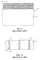
- FIG. 2is a plan view showing a substrate 44 having a partially-crystallized amorphous silicon film 52 .
- the laser beamis restricted in its width, and the mask are also restricted in its size. Therefore, when the substrate is a large size, the mask should be arranged many times over the substrate, and thus, the crystallization processes are also repeated many times corresponding to each mask arrangement.
- an area “C” corresponding to one maskis defined as one block. At this point, the crystallization of the amorphous silicon within one block “C” is achieved by irradiating the laser beam several times.
- FIGS. 3A to 3 Care plan views showing one block of an amorphous silicon film in the crystallization process steps by using a conventional SLS apparatus. At this time, it is supposed that the mask has three slits therein.
- FIG. 3Ashows an initial step of crystallizing the amorphous silicon film when a first laser beam irradiation is carried out.
- the laser beam 34 emitted from the laser generator 36passes through the mask 38 and irradiates one block of the amorphous silicon film 52 deposited on the sample substrate 44 .
- the laser beam 34is divided into three line beams by the slits “A”, and then these line beams irradiates regions “D”, “E”and “F” of the amorphous silicon film 52 in order to melt each region “D”, “E” or “F”.
- the energy density of the line beamsis sufficient to induce complete melting of the amorphous silicon film.
- the liquid phase siliconbegins to be crystallized at the interface 56 between the solid phase amorphous silicon and the liquid phase silicon. Namely, lateral grain growth of grains 58 a proceeds from the un-melted regions adjacent to the fully-melted regions. The grain boundaries in directionally solidified silicon tends to form so as to always be perpendicular to the interface 56 between the solid phase amorphous silicon and the liquid phase silicon.
- crystallized regions “D”, “E” and “F”are finally formed in one block corresponding to the mask 38 of FIG. 1, such that crystallized silicon grain regions “D”, “E” and “F” are induced.
- FIG. 3Bshows a step of crystallizing the amorphous silicon film when a second laser beam irradiation is carried out.
- the X-Y stagemoves in a direction opposite to the lateral grain growth by a distance of several micrometers that is the same as or less than the length of the lateral growth.
- the second laser beam irradiationis conducted. Therefore, the regions irradiated by the second laser beam are melted and then crystallized in the manner described in FIG. 3A.
- the silicon grains 58 a grown by the first laser beam irradiationserve as seeds for the crystallization, and thus the lateral grain growth proceeds in the melted regions.
- Silicon grains 58 b formed by the second laser beam irradiationcontinue to grow adjacent to the silicon grains 58 a formed by the first laser beam irradiation.
- FIG. 3Cshows one block of a crystalline silicon film resulted from lateral growth of grains to predetermined sizes.
- the above-mentioned crystallization processes conducted within one blockare repeated through block by block in the amorphous silicon film. Therefore, the amorphous silicon film can be converted into the crystalline silicon film although it has a large size.
- the conventional SLS apparatus described abovehas some problems as follows.
- the X-Y stagemoves by a distance of several micrometers or millimeters to induce the lateral grain growth.
- the substrate and the X-Y stageare large in size, it takes much more time to move the X-Y stage. Accordingly, the yield of crystallizing the amorphous silicon film is lowered.
- the present inventionis directed to a method and apparatus of crystallizing an amorphous silicon film using a sequential lateral solidification (SLS) that substantially obviates one or more of problems due to limitations and disadvantages of the related art.
- SLSsequential lateral solidification
- An advantage of the present inventionis to provide a sequential lateral solidification (SLS) apparatus which saves time in crystallizing an amorphous silicon film to obtain a productivity increase.
- SLSsequential lateral solidification
- Another advantage of the present inventionis to provide a method of crystallizing an amorphous silicon layer with increased manufacturing yield using the improved SLS apparatus.
- SLSsequential lateral solidification
- the above-mentioned apparatusfurther includes a condenser lens between the mask and the laser generator. Also, the condenser lens condenses the laser beam.
- the X-Y stageis movable rather long way than the mask controlled by the mask stage.
- a method of crystallizing an amorphous silicon film using the SLS apparatusincludes the steps of setting a substrate having an amorphous silicon film thereon upon the X-Y stage; applying the laser beam to the amorphous silicon film after the laser beam passes through the plurality of slits of the mask; melting first portions of the amorphous silicon film, wherein each first portion of the amorphous silicon film corresponds to each slit of the mask; crystallizing the first portions of the amorphous silicon film by the sequential lateral solidification; moving the mask by several micrometers using the mask stage; repeatedly melting and crystallizing next portions of the amorphous silicon film adjacent to the first portions whenever the mask moves by the mask stage until a lateral grain growth stops by a collision of laterally grown grains, thereby defining a block in the amorphous silicon film; moving the X-Y stage having the substrate to crystallize another block of the amorphous silicon film; and repeatedly melting and crystallizing another blocks of the a
- the laser beamirradiates the amorphous silicon film whenever the mask moves by the mask stage.
- the mask stagemoves the mask in a direction of later grain growth by a distance of several micrometers which is equal to or less than the length of the lateral growth.
- FIG. 1is a schematic configuration of a sequential lateral solidification (SLS) apparatus according to a conventional art
- FIG. 2is a plan view showing a substrate having a partially-crystallized amorphous silicon film
- FIGS. 3A to 3 Care plan views showing one block of an amorphous silicon film in the crystallization process steps using a conventional SLS apparatus;
- FIG. 4is a schematic configuration of a sequential lateral solidification (SLS) apparatus according to the present invention.
- FIG. 5A to 5 Fshows crystallization process steps of crystallizing an amorphous silicon film into a crystalline silicon film using the SLS apparatus of FIG. 4.
- FIG. 4is a schematic configuration of a sequential lateral solidification (SLS) apparatus according to the present invention.
- the SLS apparatus 132generally includes a laser generator 136 , a mask 138 , a condenser lens 140 , an objective lens 142 , an X-Y stage 146 and a mask stage 160 .
- the laser generator 136generates and emits a laser beam 134 .
- the amount of the laser beam 134 emitted from the laser generator 136is adjusted by an attenuator (not shown) that is in the path of the laser beam 134 .
- the emitted laser beam 134is then applied to the condenser lens 140 such that the laser beam 134 is condensed after passing the condenser lens 140 .
- the mask 138includes a plurality of slits “A” through which the laser beam 134 passes and light absorptive areas “B” that prevent the laser beam 134 from passing through the mask 138 .
- the width of each slit “A”defines a size of the silicon grain crystallized by a first laser irradiation.
- the distance between each slitdefines a length of the lateral grain growth when the amorphous silicon film is crystallized by the SLS method.
- the objective lens 142is arranged below the mask 138 and scales down the shape of the laser beam having passed through the mask 138 .
- An X-Y stage 146is arranged adjacent to the objective lens 142 .
- the X-Y stageis movable in two orthogonal axial directions, such as x-axis and y-axis, and includes an x-axial direction drive unit for driving the x-axis stage and a y-axial direction drive unit for driving the y-axis stage.
- a substrate 144is placed on the X-Y stage 146 in a location corresponding to the mask.
- an amorphous silicon filmis formed on the substrate 144 , thereby defining a sample substrate.
- the mask stage 160is connected to the mask 138 such that it controls movement of the mask 138 .
- the mask 138is connected to the mask stage 160 , and thus the mask 138 moves by a distance of several micrometers in accordance with a control of the mask stage 160 .
- the mask stage 160is small in size and has a small scale in moving the mask 138 , it takes little time to move and stop the mask 138 rather than the X-Y stage of the conventional art. Therefore, when the amorphous silicon film is crystallized block by block, the movement of the laser beam within one block is controlled by the mask stage 160 because the mask stage 160 minutely moves the mask 138 .
- the mask movement by the mask stage 160controls the laser beam irradiation within one block, compared the conventional art in which the laser beam irradiation is controlled by the X-Y stage. Furthermore, since the mask movement by the mask stage 160 is minute and limited within one block, the X-Y stage 146 of FIG. 4 moves the sample substrate 144 when it needs to move block by block. As a result, the crystallization time decreases when the mask stage 160 and the X-Y stage 146 are used together in the crystallization rather than when only the X-Y stage is used.
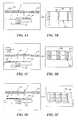
- FIGS. 5A to 5 Fshow crystallization process steps of crystallizing an amorphous silicon film into a crystalline silicon film using the SLS apparatus of FIG. 4.
- the crystallization performed within one blockwill be explained as an example.
- FIG. 5Ashows the X-Y stage 146 , the mask 138 and the mask stage 160 when initially crystallizing an amorphous silicon film 143 using a first laser beam irradiation.
- FIG. 5Bis a plan view of the substrate 144 having the amorphous silicon film 143 thereon after the first laser beam irradiation. Referring to FIGS. 5A and 5B, after the substrate 144 having the amorphous silicon film 143 is mounted on the X-Y stage 146 , the laser beam 134 emitted from the laser generator 136 passes through the mask 138 and irradiates one block of the amorphous silicon film 143 .
- the laser beam 134is divided into three line beams by the slits “A” of the mask 138 , and then these line beams irradiates regions “G”, “H” and “I” of the amorphous silicon film 143 in order to melt each region “G”, “H” or “I”.
- the liquid phase siliconrapidly begins to be crystallized at the interface 150 between the solid phase amorphous silicon and the liquid phase silicon. Namely, lateral grain growth of grains 148 a proceeds from the un-melted regions adjacent to the fully-melted regions. The grain boundaries in directionally solidified silicon tend to form so as to always be perpendicular to the interface 156 between the solid phase amorphous silicon and the liquid phase silicon.
- the mask stage 160moves the mask 138 in a direction of lateral grain growth by a distance of several micrometers which is equal to or less than the length of the lateral growth.
- FIG. 5Cshows the X-Y stage 146 , the mask 138 and the mask stage 160 when a second step of crystallizing the amorphous silicon film 143 is conducted using a second laser beam irradiation.
- FIG. 5Bis a plan view of the substrate 144 having the amorphous silicon film 143 thereon after the second laser beam irradiation. Since the mask 138 moves for the second laser beam irradiation, the slits “A” correspond to regions adjacent to the crystallized silicon grain regions “G”, “H” and “I”.
- FIG. 5 Fshows one block of a crystalline silicon film resulted from lateral growth of grains according to the present invention. Furthermore, it is noticeable in the above-mentioned SLS method that the lateral grain growth stops by making grain boundaries when the laterally grown grains collide. Therefore, the distance between each slit defines a length of the lateral grain growth, thereby controlling grain size.
- the other blocks of the amorphous silicon filmare also crystallized by the aforementioned process. Additionally in the present invention, after complete crystallization of one block the X-Y stage 146 moves the substrate a relatively long distance for the crystallization of the next block by moving the sample substrate 144 in two orthogonal axial directions, such as x-axis and y-axis. The mask stage 160 moves the mask within one block to complete crystallization within one block.
- the SLS apparatussince the SLS apparatus according to the present invention includes the mask stage that controls the minute movements of the mask, the crystallization time and the fabricating process time are reduced. Namely, it takes relatively short time to crystallize one block of the amorphous silicon film when utilizing the mask stage to move the mask rather than when utilizing the X-Y stage to move the substrate. Furthermore, the above-mentioned SLS method of crystallizing the amorphous silicon film can be adopted in crystallizing a large substrate.
Landscapes
- Engineering & Computer Science (AREA)
- Physics & Mathematics (AREA)
- Optics & Photonics (AREA)
- Computer Hardware Design (AREA)
- Condensed Matter Physics & Semiconductors (AREA)
- General Physics & Mathematics (AREA)
- Manufacturing & Machinery (AREA)
- Microelectronics & Electronic Packaging (AREA)
- Power Engineering (AREA)
- Chemical & Material Sciences (AREA)
- Crystallography & Structural Chemistry (AREA)
- Plasma & Fusion (AREA)
- Mechanical Engineering (AREA)
- Materials Engineering (AREA)
- Recrystallisation Techniques (AREA)
- Thin Film Transistor (AREA)
Abstract
Description
- This application claims the benefit of Korean Patent Application No. 2000-83763, filed on Dec. 28, 2000 in Korea, which is hereby incorporated by reference as it sully set forth herein.[0001]
- 1. Field of the Invention[0002]
- The present invention relates to an apparatus and method of crystallizing an amorphous silicon film, and more particularly, to a sequential lateral solidification (SLS) apparatus and a crystallization method using the SLS apparatus.[0003]
- 2. Discussion of Related Art[0004]
- Generally, polycrystalline silicon (p-Si) or amorphous silicon (a-Si) are materials used as the active layer of thin film transistor (TFTs) in liquid crystal display (LCD) devices. Since amorphous silicon (a-Si) can be deposited at a low temperature to form a thin film on a glass substrate, it is more widely used as an element of a switching device in liquid crystal display (LCD) devices. However, amorphous silicon (a-Si) has a difficulty in being employed in the large LCD devices because of its electrical characteristics.[0005]
- In contrast to amorphous silicon, polycrystalline silicon provides faster display response time when used as an element of the TFT. Thus, polycrystalline silicon (p-Si) can be used in the large-sized LCD devices, laptop computers and wall television sets which need a larger field effect mobility of more than 30 cm[0006]2/Vs and a low leakage current.
- Polycrystalline silicon is composed of crystal grains and grain boundaries. If the grains are larger and the grain boundaries are regularly distributed within the polycrystalline silicon, the field effect mobility becomes larger. In view of these grains and grain boundaries, a silicon crystallization method that produces large grains currently becomes an important issue. Accordingly, a sequential lateral solidification (SLS), which induces lateral growth of silicon grains to form single-crystal silicon film using laser energy, is proposed.[0007]
- The SLS method of crystallizing an amorphous silicon layer uses the fact that silicon grains tend to grow vertically against the interface between liquid and solid silicon, and teaches that the amorphous silicon layer is crystallized by controlling the magnitude of laser energy and an irradiation of a moving laser beam to form silicon grains growing latterly up to a predetermined length. Therefore, to conduct the SLS method, an SLS apparatus is required as shown in FIG. 1.[0008]
- FIG.[0009]1 is a schematic configuration of a sequential lateral solidification (SLS) apparatus according to a conventional art. In FIG. 1, the
SLS apparatus 32 widely includes alaser generator 36, amask 38, acondenser lens 40 and anobjective lens 42. Thelaser generator 36 generates and emits alaser beam 34. The amount of thelaser beam 34 emitted from thelaser generator 36 is adjusted by an attenuator (not shown) that is in the path of thelaser beam 34. The emittedlaser beam 34 is applied to thecondenser lens 40 such that thelaser beam 34 is condensed after passing thecondenser lens 40. Themask 38 includes a plurality of slits “A” through which thelaser beam 34 passes and light absorptive areas “B” that absorb thelaser beam 34. At this point, the width of each slit “A” defines a size of the grain when amorphous silicon is crystallized by a first laser irradiation. Furthermore, the distance between each slit defines a size of the lateral grain growth when the amorphous silicon film is crystallized by the SLS method. Theobjective lens 42 is arranged below the mask and scales down the shape of the laser beam having passed through themask 38. - Further in FIG. 1, an[0010]
X-Y stage 46 is arranged adjacent to theobjective lens 42. The X-Y stage is movable in two orthogonal axial directions, such as x-axis and y-axis, and includes an x-axial direction drive unit for driving the x-axis stage and a y-axial direction drive unit for driving the y-axis stage. Asubstrate 44 is placed on theX-Y stage 46 in a location corresponding to the mask. Although not shown in FIG. 1, an amorphous silicon film is formed on thesubstrate 44, thereby defining a sample substrate. In this conventional configuration of the SLS apparatus, thelaser generator 36 and themask 38 are fixed in a corresponding position such that themask 38 is not movable to crystallize the amorphous silicon film of thesample substrate 44. Thus, the X-Y stage should minutely move in an x-axial or y-axial direction to crystallize all thesample substrate 44. - A method of crystallizing an amorphous silicon film using the above-described SLS apparatus is explained hereinafter. A crystalline silicon film is generally formed by crystallizing the amorphous silicon film previously deposited on a substrate. The amorphous silicon film is deposited on the substrate using a chemical vapor deposition (CVD) method and includes a lot of hydrogen therein. The amorphous silicon film is thermal-treated to conduct the de-hydrogenation thereof, thereby reducing the amount of the hydrogen contained in the amorphous silicon film. The reason for the de-hydrogenation is to make a surface of the crystalline silicon film smooth. If the de-hydrogenation is not conducted, the surface of the crystalline silicon film becomes rough, and thus the electrical characteristics of the crystalline silicon film become degraded.[0011]
- FIG. 2 is a plan view showing a[0012]
substrate 44 having a partially-crystallizedamorphous silicon film 52. When crystallizing the amorphous silicon film using the laser beam, it is difficult to crystallize a whole region of the amorphous silicon film at one time because the laser beam is restricted in its width, and the mask are also restricted in its size. Therefore, when the substrate is a large size, the mask should be arranged many times over the substrate, and thus, the crystallization processes are also repeated many times corresponding to each mask arrangement. In FIG. 2, an area “C” corresponding to one mask is defined as one block. At this point, the crystallization of the amorphous silicon within one block “C” is achieved by irradiating the laser beam several times. - The crystallization process of the amorphous silicon film will be explained as follows. FIGS. 3A to[0013]3C are plan views showing one block of an amorphous silicon film in the crystallization process steps by using a conventional SLS apparatus. At this time, it is supposed that the mask has three slits therein.
- FIG. 3A shows an initial step of crystallizing the amorphous silicon film when a first laser beam irradiation is carried out. As described in FIG. 1, the[0014]
laser beam 34 emitted from thelaser generator 36 passes through themask 38 and irradiates one block of theamorphous silicon film 52 deposited on thesample substrate 44. At this time, thelaser beam 34 is divided into three line beams by the slits “A”, and then these line beams irradiates regions “D”, “E”and “F” of theamorphous silicon film 52 in order to melt each region “D”, “E” or “F”. The energy density of the line beams is sufficient to induce complete melting of the amorphous silicon film. The liquid phase silicon begins to be crystallized at theinterface 56 between the solid phase amorphous silicon and the liquid phase silicon. Namely, lateral grain growth ofgrains 58aproceeds from the un-melted regions adjacent to the fully-melted regions. The grain boundaries in directionally solidified silicon tends to form so as to always be perpendicular to theinterface 56 between the solid phase amorphous silicon and the liquid phase silicon. As a result of the first laser beam irradiation, crystallized regions “D”, “E” and “F” are finally formed in one block corresponding to themask 38 of FIG. 1, such that crystallized silicon grain regions “D”, “E” and “F” are induced. - FIG. 3B shows a step of crystallizing the amorphous silicon film when a second laser beam irradiation is carried out. After the first laser beam irradiation, the X-Y stage moves in a direction opposite to the lateral grain growth by a distance of several micrometers that is the same as or less than the length of the lateral growth. Then, the second laser beam irradiation is conducted. Therefore, the regions irradiated by the second laser beam are melted and then crystallized in the manner described in FIG. 3A. At this time, the[0015]
silicon grains 58agrown by the first laser beam irradiation serve as seeds for the crystallization, and thus the lateral grain growth proceeds in the melted regions.Silicon grains 58bformed by the second laser beam irradiation continue to grow adjacent to thesilicon grains 58aformed by the first laser beam irradiation. - Accordingly, by repeating the foregoing steps of melting and crystallizing the amorphous silicon, one block of the amorphous silicon film is crystallized to form[0016]
grains 58cas shown in FIG. 3C. FIG. 3C shows one block of a crystalline silicon film resulted from lateral growth of grains to predetermined sizes. - Moreover, the above-mentioned crystallization processes conducted within one block are repeated through block by block in the amorphous silicon film. Therefore, the amorphous silicon film can be converted into the crystalline silicon film although it has a large size. However, the conventional SLS apparatus described above has some problems as follows.[0017]
- First, in the crystallization process which uses the laser beam passing through the slits of the mask, the X-Y stage moves by a distance of several micrometers or millimeters to induce the lateral grain growth. However, it is very difficult to control the movement distance using the relatively large X-Y stage. Second, it takes 0.1 to 1 seconds that the X-Y stage moves and stops. However, if the substrate and the X-Y stage are large in size, it takes much more time to move the X-Y stage. Accordingly, the yield of crystallizing the amorphous silicon film is lowered.[0018]
- Accordingly, the present invention is directed to a method and apparatus of crystallizing an amorphous silicon film using a sequential lateral solidification (SLS) that substantially obviates one or more of problems due to limitations and disadvantages of the related art.[0019]
- An advantage of the present invention is to provide a sequential lateral solidification (SLS) apparatus which saves time in crystallizing an amorphous silicon film to obtain a productivity increase.[0020]
- Another advantage of the present invention is to provide a method of crystallizing an amorphous silicon layer with increased manufacturing yield using the improved SLS apparatus.[0021]
- Additional features and advantages of the invention will be set forth in the description which follows, and in part will be apparent from the description, or may be learned by practice of the invention. The objectives and other advantages of the invention will be realized and attained by the method particularly pointed out in the written description and claims hereof as well as the appended drawings.[0022]
- To achieve these and other advantages and in accordance with the purpose of the present invention, as embodied and broadly described, a sequential lateral solidification (SLS) apparatus for crystallizing an amorphous silicon film includes a laser generator generating and emitting a laser beam;an X-Y stage corresponding to the laser generator and moving in two orthogonal axial directions; a mask arranged between the laser generator and the X-Y stage, the mask having a plurality of slits through which the laser beam passes; an objective lens arranged between the mask and the X-Y stage, the objective lens scaling down the laser beam; and a mask stage connected to the mask, the mask stage controlling a minute movement of the mask.[0023]
- The above-mentioned apparatus further includes a condenser lens between the mask and the laser generator. Also, the condenser lens condenses the laser beam. In the above SLS apparatus, the X-Y stage is movable rather long way than the mask controlled by the mask stage.[0024]
- In another aspect, a method of crystallizing an amorphous silicon film using the SLS apparatus includes the steps of setting a substrate having an amorphous silicon film thereon upon the X-Y stage; applying the laser beam to the amorphous silicon film after the laser beam passes through the plurality of slits of the mask; melting first portions of the amorphous silicon film, wherein each first portion of the amorphous silicon film corresponds to each slit of the mask; crystallizing the first portions of the amorphous silicon film by the sequential lateral solidification; moving the mask by several micrometers using the mask stage; repeatedly melting and crystallizing next portions of the amorphous silicon film adjacent to the first portions whenever the mask moves by the mask stage until a lateral grain growth stops by a collision of laterally grown grains, thereby defining a block in the amorphous silicon film; moving the X-Y stage having the substrate to crystallize another block of the amorphous silicon film; and repeatedly melting and crystallizing another blocks of the amorphous silicon film whenever the X-Y stage moves.[0025]
- In the above method, the laser beam irradiates the amorphous silicon film whenever the mask moves by the mask stage. Beneficially, the mask stage moves the mask in a direction of later grain growth by a distance of several micrometers which is equal to or less than the length of the lateral growth.[0026]
- It is to be understood that both the foregoing general description and the following detailed description are exemplary and explanatory and are intended to provide further explanation of the invention as claimed.[0027]
- The accompanying drawings, which are included to provide a further understanding of the invention and are incorporated in and constitute a part of this application, illustrate embodiments of the invention and together with the description serve to explain the principle of the invention.[0028]
- In the drawings:[0029]
- FIG. 1 is a schematic configuration of a sequential lateral solidification (SLS) apparatus according to a conventional art;[0030]
- FIG. 2 is a plan view showing a substrate having a partially-crystallized amorphous silicon film;[0031]
- FIGS. 3A to[0032]3C are plan views showing one block of an amorphous silicon film in the crystallization process steps using a conventional SLS apparatus;
- FIG. 4 is a schematic configuration of a sequential lateral solidification (SLS) apparatus according to the present invention; and[0033]
- FIGS. 5A to[0034]5F shows crystallization process steps of crystallizing an amorphous silicon film into a crystalline silicon film using the SLS apparatus of FIG. 4.
- Reference will now be made in detail to the preferred embodiments of the present invention, examples of which are shown in the accompanying drawings. Wherever possible, similar reference numbers will be used throughout the drawings to refer to the same or like parts.[0035]
- FIG. 4 is a schematic configuration of a sequential lateral solidification (SLS) apparatus according to the present invention. In FIG. 4, the[0036]
SLS apparatus 132 generally includes alaser generator 136, amask 138, acondenser lens 140, anobjective lens 142, anX-Y stage 146 and amask stage 160. Thelaser generator 136 generates and emits alaser beam 134. The amount of thelaser beam 134 emitted from thelaser generator 136 is adjusted by an attenuator (not shown) that is in the path of thelaser beam 134. The emittedlaser beam 134 is then applied to thecondenser lens 140 such that thelaser beam 134 is condensed after passing thecondenser lens 140. Themask 138 includes a plurality of slits “A” through which thelaser beam 134 passes and light absorptive areas “B” that prevent thelaser beam 134 from passing through themask 138. At this point, the width of each slit “A” defines a size of the silicon grain crystallized by a first laser irradiation. Furthermore, the distance between each slit defines a length of the lateral grain growth when the amorphous silicon film is crystallized by the SLS method. - Still referring to FIG. 4, the[0037]
objective lens 142 is arranged below themask 138 and scales down the shape of the laser beam having passed through themask 138. AnX-Y stage 146 is arranged adjacent to theobjective lens 142. The X-Y stage is movable in two orthogonal axial directions, such as x-axis and y-axis, and includes an x-axial direction drive unit for driving the x-axis stage and a y-axial direction drive unit for driving the y-axis stage. Asubstrate 144 is placed on theX-Y stage 146 in a location corresponding to the mask. Although not shown in FIG. 4, an amorphous silicon film is formed on thesubstrate 144, thereby defining a sample substrate. - In the present invention, the[0038]
mask stage 160 is connected to themask 138 such that it controls movement of themask 138. Namely, themask 138 is connected to themask stage 160, and thus themask 138 moves by a distance of several micrometers in accordance with a control of themask stage 160. Since themask stage 160 is small in size and has a small scale in moving themask 138, it takes little time to move and stop themask 138 rather than the X-Y stage of the conventional art. Therefore, when the amorphous silicon film is crystallized block by block, the movement of the laser beam within one block is controlled by themask stage 160 because themask stage 160 minutely moves themask 138. Namely, the mask movement by themask stage 160 controls the laser beam irradiation within one block, compared the conventional art in which the laser beam irradiation is controlled by the X-Y stage. Furthermore, since the mask movement by themask stage 160 is minute and limited within one block, theX-Y stage 146 of FIG. 4 moves thesample substrate 144 when it needs to move block by block. As a result, the crystallization time decreases when themask stage 160 and theX-Y stage 146 are used together in the crystallization rather than when only the X-Y stage is used. - FIGS. 5A to[0039]5F show crystallization process steps of crystallizing an amorphous silicon film into a crystalline silicon film using the SLS apparatus of FIG. 4. In FIGS. 5A to5F, the crystallization performed within one block will be explained as an example.
- FIG. 5A shows the[0040]
X-Y stage 146, themask 138 and themask stage 160 when initially crystallizing anamorphous silicon film 143 using a first laser beam irradiation. FIG. 5B is a plan view of thesubstrate 144 having theamorphous silicon film 143 thereon after the first laser beam irradiation. Referring to FIGS. 5A and 5B, after thesubstrate 144 having theamorphous silicon film 143 is mounted on theX-Y stage 146, thelaser beam 134 emitted from thelaser generator 136 passes through themask 138 and irradiates one block of theamorphous silicon film 143. At this time, thelaser beam 134 is divided into three line beams by the slits “A” of themask 138, and then these line beams irradiates regions “G”, “H” and “I” of theamorphous silicon film 143 in order to melt each region “G”, “H” or “I”. When the first laser beam irradiation is stopped, the liquid phase silicon rapidly begins to be crystallized at theinterface 150 between the solid phase amorphous silicon and the liquid phase silicon. Namely, lateral grain growth ofgrains 148aproceeds from the un-melted regions adjacent to the fully-melted regions. The grain boundaries in directionally solidified silicon tend to form so as to always be perpendicular to the interface156 between the solid phase amorphous silicon and the liquid phase silicon. As a result of the first laser beam irradiation, crystallized regions “G”, “H” and “I” of FIG. 5B are finally formed in one block corresponding to themask 138 of FIG. 5B, such that the crystallized silicon grain regions “G”, “H” and “I” are induced. At this time of conducting the first laser beam irradiation, the width of each slit “A” defines the size of thegrain 148a. - After the first laser beam irradiation process shown in FIGS. 5A and 5B, the[0041]
mask stage 160 moves themask 138 in a direction of lateral grain growth by a distance of several micrometers which is equal to or less than the length of the lateral growth. - FIG. 5C shows the[0042]
X-Y stage 146, themask 138 and themask stage 160 when a second step of crystallizing theamorphous silicon film 143 is conducted using a second laser beam irradiation. FIG. 5B is a plan view of thesubstrate 144 having theamorphous silicon film 143 thereon after the second laser beam irradiation. Since themask 138 moves for the second laser beam irradiation, the slits “A” correspond to regions adjacent to the crystallized silicon grain regions “G”, “H” and “I”. - When the second laser beam irradiation is conducted, the regions adjacent to the crystallized silicon grain regions “G”, “H” and “I” of FIG. 5B are melted by the three line beams. Thereafter, when the second laser beam irradiation is stopped, the[0043]
silicon grains 148a(see FIG. 5B) grown by the first laser beam irradiation serve as seeds for the crystallization, and thus, the lateral grain growth proceeds in the melted regions.Silicon grains 148bare finally formed by the second laser beam irradiation. - Accordingly, by repeating the foregoing steps of melting and crystallizing the amorphous silicon as described in FIG. 5E, one block of the amorphous silicon film is crystallized to form[0044]
grains 148cas shown in FIG. 5F. Namely, FIG5F shows one block of a crystalline silicon film resulted from lateral growth of grains according to the present invention. Furthermore, it is noticeable in the above-mentioned SLS method that the lateral grain growth stops by making grain boundaries when the laterally grown grains collide. Therefore, the distance between each slit defines a length of the lateral grain growth, thereby controlling grain size. - After crystallizing one block of the amorphous silicon film, the other blocks of the amorphous silicon film are also crystallized by the aforementioned process. Additionally in the present invention, after complete crystallization of one block the[0045]
X-Y stage 146 moves the substrate a relatively long distance for the crystallization of the next block by moving thesample substrate 144 in two orthogonal axial directions, such as x-axis and y-axis. Themask stage 160 moves the mask within one block to complete crystallization within one block. - As described before, since the SLS apparatus according to the present invention includes the mask stage that controls the minute movements of the mask, the crystallization time and the fabricating process time are reduced. Namely, it takes relatively short time to crystallize one block of the amorphous silicon film when utilizing the mask stage to move the mask rather than when utilizing the X-Y stage to move the substrate. Furthermore, the above-mentioned SLS method of crystallizing the amorphous silicon film can be adopted in crystallizing a large substrate.[0046]
- It will be apparent to those skilled in the art that various modifications and variations can be made in the method of crystallizing the amorphous silicon without departing from the spirit or scope of the inventions. Thus, it is intended that the present invention cover the modifications and variations of this invention provided they come within the scope of the appended claims and their equivalents.[0047]
Claims (14)
Priority Applications (1)
| Application Number | Priority Date | Filing Date | Title |
|---|---|---|---|
| US12/071,915US20080149029A1 (en) | 2000-12-28 | 2008-02-27 | Apparatus and method of crystallizing amorphous silicon |
Applications Claiming Priority (2)
| Application Number | Priority Date | Filing Date | Title |
|---|---|---|---|
| KR10-2000-0083763AKR100400510B1 (en) | 2000-12-28 | 2000-12-28 | A machine for Si crystallization and method of crystallizing Si |
| KR2000-83763 | 2000-12-28 |
Related Child Applications (1)
| Application Number | Title | Priority Date | Filing Date |
|---|---|---|---|
| US12/071,915ContinuationUS20080149029A1 (en) | 2000-12-28 | 2008-02-27 | Apparatus and method of crystallizing amorphous silicon |
Publications (2)
| Publication Number | Publication Date |
|---|---|
| US20020083557A1true US20020083557A1 (en) | 2002-07-04 |
| US7357963B2 US7357963B2 (en) | 2008-04-15 |
Family
ID=19703761
Family Applications (2)
| Application Number | Title | Priority Date | Filing Date |
|---|---|---|---|
| US10/025,907Expired - LifetimeUS7357963B2 (en) | 2000-12-28 | 2001-12-26 | Apparatus and method of crystallizing amorphous silicon |
| US12/071,915AbandonedUS20080149029A1 (en) | 2000-12-28 | 2008-02-27 | Apparatus and method of crystallizing amorphous silicon |
Family Applications After (1)
| Application Number | Title | Priority Date | Filing Date |
|---|---|---|---|
| US12/071,915AbandonedUS20080149029A1 (en) | 2000-12-28 | 2008-02-27 | Apparatus and method of crystallizing amorphous silicon |
Country Status (3)
| Country | Link |
|---|---|
| US (2) | US7357963B2 (en) |
| JP (1) | JP4263403B2 (en) |
| KR (1) | KR100400510B1 (en) |
Cited By (38)
| Publication number | Priority date | Publication date | Assignee | Title |
|---|---|---|---|---|
| US20020197759A1 (en)* | 2001-06-07 | 2002-12-26 | Myoung-Su Yang | Amorphous silicon crystallization method |
| WO2004023538A1 (en)* | 2002-09-09 | 2004-03-18 | Sharp Kabushiki Kaisha | Crystal growing method, crystal growing apparatus, beam splitter, and display |
| WO2004038775A1 (en)* | 2002-10-22 | 2004-05-06 | Samsung Electronics Co., Ltd. | Method of polycyrstallization, method of manufacturing polysilicon thin film transistor, and laser irradiation device therefor |
| US20040144988A1 (en)* | 2002-12-31 | 2004-07-29 | Lg. Philips Lcd Co., Ltd. | Active matric display device including polycrystalline silicon thin film transistor and manufacturing method of the same |
| US20050059265A1 (en)* | 2003-09-16 | 2005-03-17 | The Trustees Of Columbia University In The City Of New York | Systems and methods for processing thin films |
| US20050059223A1 (en)* | 2003-09-16 | 2005-03-17 | The Trustees Of Columbia University | Laser-irradiated thin films having variable thickness |
| US20050059224A1 (en)* | 2003-09-16 | 2005-03-17 | The Trustees Of Columbia University In The City Of New York | Systems and methods for inducing crystallization of thin films using multiple optical paths |
| US20050130357A1 (en)* | 2001-12-17 | 2005-06-16 | Samsung Electronics Co. Ltd. | Method for manufacturing a thin film transistor using poly silicon |
| WO2005029550A3 (en)* | 2003-09-16 | 2005-09-09 | Univ Columbia | Method and system for producing crystalline thin films with a uniform crystalline orientation |
| US20050235903A1 (en)* | 2003-09-19 | 2005-10-27 | The Trustees Of Columbia University In The City Of New York | Single scan irradiation for crystallization of thin films |
| WO2006055003A1 (en)* | 2004-11-18 | 2006-05-26 | The Trustees Of Columbia University In The City Ofnew York | Systems and methods for creating crystallographic-orientation controlled poly-silicon films |
| US20070187846A1 (en)* | 2001-11-14 | 2007-08-16 | Myung-Koo Kang | Mask for crystallizing polysilicon and a method for forming thin film transistor using the mask |
| US20080011726A1 (en)* | 2003-12-24 | 2008-01-17 | Seo Hyun S | Method of deciding focal plane and method of crystallization using thereof |
| US7622370B2 (en) | 2002-08-19 | 2009-11-24 | The Trustees Of Columbia University In The City Of New York | Process and system for laser crystallization processing of film regions on a substrate to minimize edge areas, and a structure of such film regions |
| US7638728B2 (en) | 2003-09-16 | 2009-12-29 | The Trustees Of Columbia University In The City Of New York | Enhancing the width of polycrystalline grains with mask |
| US7645337B2 (en) | 2004-11-18 | 2010-01-12 | The Trustees Of Columbia University In The City Of New York | Systems and methods for creating crystallographic-orientation controlled poly-silicon films |
| US7679028B2 (en) | 1996-05-28 | 2010-03-16 | The Trustees Of Columbia University In The City Of New York | Methods for producing uniform large-grained and grain boundary location manipulated polycrystalline thin film semiconductors using sequential lateral solidification |
| US7704862B2 (en) | 2000-03-21 | 2010-04-27 | The Trustees Of Columbia University | Surface planarization of thin silicon films during and after processing by the sequential lateral solidification method |
| US7709378B2 (en) | 2000-10-10 | 2010-05-04 | The Trustees Of Columbia University In The City Of New York | Method and apparatus for processing thin metal layers |
| US7718517B2 (en) | 2002-08-19 | 2010-05-18 | Im James S | Single-shot semiconductor processing system and method having various irradiation patterns |
| US7759230B2 (en) | 2003-09-16 | 2010-07-20 | The Trustees Of Columbia University In The City Of New York | System for providing a continuous motion sequential lateral solidification for reducing or eliminating artifacts in overlap regions, and a mask for facilitating such artifact reduction/elimination |
| US7902052B2 (en) | 2003-02-19 | 2011-03-08 | The Trustees Of Columbia University In The City Of New York | System and process for processing a plurality of semiconductor thin films which are crystallized using sequential lateral solidification techniques |
| US8012861B2 (en) | 2007-11-21 | 2011-09-06 | The Trustees Of Columbia University In The City Of New York | Systems and methods for preparing epitaxially textured polycrystalline films |
| US8221544B2 (en) | 2005-04-06 | 2012-07-17 | The Trustees Of Columbia University In The City Of New York | Line scan sequential lateral solidification of thin films |
| US8415670B2 (en) | 2007-09-25 | 2013-04-09 | The Trustees Of Columbia University In The City Of New York | Methods of producing high uniformity in thin film transistor devices fabricated on laterally crystallized thin films |
| US8426296B2 (en) | 2007-11-21 | 2013-04-23 | The Trustees Of Columbia University In The City Of New York | Systems and methods for preparing epitaxially textured polycrystalline films |
| US8440581B2 (en) | 2009-11-24 | 2013-05-14 | The Trustees Of Columbia University In The City Of New York | Systems and methods for non-periodic pulse sequential lateral solidification |
| US8557040B2 (en) | 2007-11-21 | 2013-10-15 | The Trustees Of Columbia University In The City Of New York | Systems and methods for preparation of epitaxially textured thick films |
| US8569155B2 (en) | 2008-02-29 | 2013-10-29 | The Trustees Of Columbia University In The City Of New York | Flash lamp annealing crystallization for large area thin films |
| US8598588B2 (en) | 2005-12-05 | 2013-12-03 | The Trustees Of Columbia University In The City Of New York | Systems and methods for processing a film, and thin films |
| US8614471B2 (en) | 2007-09-21 | 2013-12-24 | The Trustees Of Columbia University In The City Of New York | Collections of laterally crystallized semiconductor islands for use in thin film transistors |
| US8663387B2 (en) | 2003-09-16 | 2014-03-04 | The Trustees Of Columbia University In The City Of New York | Method and system for facilitating bi-directional growth |
| US8796159B2 (en) | 2003-09-16 | 2014-08-05 | The Trustees Of Columbia University In The City Of New York | Processes and systems for laser crystallization processing of film regions on a substrate utilizing a line-type beam, and structures of such film regions |
| US8802580B2 (en) | 2008-11-14 | 2014-08-12 | The Trustees Of Columbia University In The City Of New York | Systems and methods for the crystallization of thin films |
| CN104538307A (en)* | 2014-12-19 | 2015-04-22 | 深圳市华星光电技术有限公司 | Polycrystalline silicon thin film transistor manufacturing method |
| US9087696B2 (en) | 2009-11-03 | 2015-07-21 | The Trustees Of Columbia University In The City Of New York | Systems and methods for non-periodic pulse partial melt film processing |
| US9646831B2 (en) | 2009-11-03 | 2017-05-09 | The Trustees Of Columbia University In The City Of New York | Advanced excimer laser annealing for thin films |
| US11413704B2 (en)* | 2019-07-17 | 2022-08-16 | Fanuc Corporation | Adjustment assistance device and laser welding apparatus |
Families Citing this family (14)
| Publication number | Priority date | Publication date | Assignee | Title |
|---|---|---|---|---|
| KR100478758B1 (en)* | 2002-04-16 | 2005-03-24 | 엘지.필립스 엘시디 주식회사 | A method for crystallizing of an amorphous Si |
| KR100878240B1 (en)* | 2002-09-16 | 2009-01-13 | 삼성전자주식회사 | Polycrystalline mask and manufacturing method of thin film transistor using same |
| KR100878243B1 (en)* | 2002-10-04 | 2009-01-13 | 삼성전자주식회사 | Method of manufacturing polycrystalline silicon thin film transistor |
| KR100492152B1 (en) | 2002-12-31 | 2005-06-01 | 엘지.필립스 엘시디 주식회사 | A method for crystallizing of an amorphous Si |
| DE10301482A1 (en)* | 2003-01-16 | 2004-07-29 | Microlas Lasersystem Gmbh | Process and device to crystallize amorphous semiconductor especially amorphous silicon layers uses at least two successive melting radiation pulses separated by one microsecond |
| KR100720452B1 (en)* | 2003-06-30 | 2007-05-22 | 엘지.필립스 엘시디 주식회사 | Laser irradiation apparatus and silicon crystallization method using the same |
| KR100546711B1 (en)* | 2003-08-18 | 2006-01-26 | 엘지.필립스 엘시디 주식회사 | Laser irradiation apparatus and silicon crystallization method using the same |
| KR100525443B1 (en) | 2003-12-24 | 2005-11-02 | 엘지.필립스 엘시디 주식회사 | Device for Crystallization and method for Crystallization with the same |
| JP4834853B2 (en) | 2004-06-10 | 2011-12-14 | シャープ株式会社 | THIN FILM TRANSISTOR CIRCUIT, THIN FILM TRANSISTOR CIRCUIT DESIGN METHOD, THIN FILM TRANSISTOR CIRCUIT DESIGN PROGRAM, DESIGN PROGRAM RECORDING MEDIUM, AND DISPLAY DEVICE |
| KR100689315B1 (en) | 2004-08-10 | 2007-03-08 | 엘지.필립스 엘시디 주식회사 | Silicon Thin Film Crystallization Apparatus and Crystallization Method Using The Same |
| TW201427990A (en) | 2013-01-09 | 2014-07-16 | Univ Nat Cheng Kung | High efficient dengue vaccine with biodegradability, preparing method and pharmaceutical composition of the same |
| CN103887157B (en)* | 2014-03-12 | 2021-08-27 | 京东方科技集团股份有限公司 | Optical mask plate and laser stripping device |
| CN109062001B (en)* | 2018-08-27 | 2022-04-08 | 京东方科技集团股份有限公司 | Mask plate |
| CN112808549B (en)* | 2021-02-02 | 2024-05-31 | 北京梦之墨科技有限公司 | Light treatment equipment |
Citations (42)
| Publication number | Priority date | Publication date | Assignee | Title |
|---|---|---|---|---|
| US6495405B2 (en)* | 2001-01-29 | 2002-12-17 | Sharp Laboratories Of America, Inc. | Method of optimizing channel characteristics using laterally-crystallized ELA poly-Si films |
| US20040060504A1 (en)* | 2002-09-30 | 2004-04-01 | Hitachi, Ltd. | Semiconductor thin film and process for production thereof |
| US20040076894A1 (en)* | 2002-10-04 | 2004-04-22 | Lg. Philips Lcd Co., Ltd. | Mask and method for crystallizing amorphous silicon |
| US20040135205A1 (en)* | 2002-12-30 | 2004-07-15 | Yun-Ho Jung | Liquid crystal display device having drive circuit and fabricating method thereof |
| US6767804B2 (en)* | 2001-11-08 | 2004-07-27 | Sharp Laboratories Of America, Inc. | 2N mask design and method of sequential lateral solidification |
| US6770545B2 (en)* | 2001-06-07 | 2004-08-03 | Lg Philips Lcd Co., Ltd. | Amorphous silicon crystallization method |
| US6777276B2 (en)* | 2002-08-29 | 2004-08-17 | Sharp Laboratories Of America, Inc. | System and method for optimized laser annealing smoothing mask |
| US20040201019A1 (en)* | 2003-01-08 | 2004-10-14 | Hyun-Jae Kim | Polysilicon thin film transistor array panel and manufacturing method thereof |
| US20040235279A1 (en)* | 2003-05-20 | 2004-11-25 | Kim Young-Joo | Method of fabricating polycrystalline silicon and switching device using polycrystalline silicon |
| US20040266146A1 (en)* | 2003-06-30 | 2004-12-30 | Jung Yun Ho | Laser crystallizing device and method for crystallizing silicon by using the same |
| US20050040148A1 (en)* | 2003-08-18 | 2005-02-24 | Jung Yun Ho | Laser crystallizing device and method for crystallizing silicon by using the same |
| US6867151B2 (en)* | 2002-12-31 | 2005-03-15 | Lg. Philips Lcd Co., Ltd. | Mask for sequential lateral solidification and crystallization method using thereof |
| US20050095762A1 (en)* | 2002-05-23 | 2005-05-05 | Sang-Hyun Kim | Mask for crystallizing and method of crystallizing amorphous silicon using the same |
| US6908835B2 (en)* | 2001-04-19 | 2005-06-21 | The Trustees Of Columbia University In The City Of New York | Method and system for providing a single-scan, continuous motion sequential lateral solidification |
| US20050142452A1 (en)* | 2003-12-29 | 2005-06-30 | You Jaesung | Laser mask and method of crystallization using the same |
| US20050142299A1 (en)* | 2003-12-29 | 2005-06-30 | Kim Eok S. | Method for forming polycrystalline silicon film of polycrystalline silicon TFT |
| US20050142453A1 (en)* | 2003-12-24 | 2005-06-30 | Seo Hyun S. | Laser mask and crystallization method using the same |
| US20050142450A1 (en)* | 2003-12-26 | 2005-06-30 | Lg.Philips Lcd Co., Ltd. | Laser beam pattern mask and crystallization method using the same |
| US20050139925A1 (en)* | 2003-12-29 | 2005-06-30 | You Jaesung | Laser mask and crystallization method using the same |
| US20050173752A1 (en)* | 2004-01-06 | 2005-08-11 | Ui-Jin Chung | Optic mask and manufacturing method of thin film transistor array panel using the same |
| US20050181136A1 (en)* | 2001-05-30 | 2005-08-18 | Yun-Ho Jung | Amorphous silicon deposition for sequential lateral solidification |
| US20050202654A1 (en)* | 2002-08-19 | 2005-09-15 | Im James S. | Process and system for laser crystallization processing of film regions on a substrate to provide substantial uniformity, and a structure of such film regions |
| US6946367B2 (en)* | 2002-02-28 | 2005-09-20 | Kabushiki Kaisha Ekisho Sentan Gijutsu Kaihatsu Center | Methods for forming a semiconductor thin film |
| US6949422B2 (en)* | 2002-12-31 | 2005-09-27 | Lg Philips Lcd Co., Ltd. | Method of crystalizing amorphous silicon for use in thin film transistor |
| US20050233511A1 (en)* | 2004-04-14 | 2005-10-20 | You Jaesung | Laser mask and method of crystallization using the same |
| US20050235903A1 (en)* | 2003-09-19 | 2005-10-27 | The Trustees Of Columbia University In The City Of New York | Single scan irradiation for crystallization of thin films |
| US6961117B2 (en)* | 2000-11-27 | 2005-11-01 | The Trustees Of Columbia University In The City Of New York | Process and mask projection system for laser crystallization processing of semiconductor film regions on a substrate |
| US20050271952A1 (en)* | 2004-06-04 | 2005-12-08 | Lg.Philips Lcd Co., Ltd. | Laser beam pattern mask and crystallization method using the same |
| US20060003506A1 (en)* | 2004-06-30 | 2006-01-05 | Lg.Philips Lcd Co., Ltd. | Crystallization method and apparatus thereof |
| US6984573B2 (en)* | 2002-06-14 | 2006-01-10 | Semiconductor Energy Laboratory Co., Ltd. | Laser irradiation method and apparatus |
| US6989300B1 (en)* | 1999-07-13 | 2006-01-24 | Nec Corporation | Method for forming semiconductor films at desired positions on a substrate |
| US20060035478A1 (en)* | 2004-08-10 | 2006-02-16 | Lg Philips Lcd Co., Ltd. | Variable mask device for crystallizing silicon layer and method for crystallizing using the same |
| US20060040512A1 (en)* | 2002-08-19 | 2006-02-23 | Im James S | Single-shot semiconductor processing system and method having various irradiation patterns |
| US7008863B2 (en)* | 2003-12-29 | 2006-03-07 | Boe Hydis Technology Co., Ltd. | Method for forming polycrystalline silicon film |
| US20060060130A1 (en)* | 2002-08-19 | 2006-03-23 | Im James S | Process and system for laser crystallization processing of film regions on a substrate to provide substantial uniformity within arears in such regions and edge areas thereof, and a structure of film regions |
| US20060065186A1 (en)* | 2002-12-10 | 2006-03-30 | Canon Kabushiki Kaisha | Process for producing crystalline thin film |
| US20060102901A1 (en)* | 2004-11-18 | 2006-05-18 | The Trustees Of Columbia University In The City Of New York | Systems and methods for creating crystallographic-orientation controlled poly-Silicon films |
| US7064016B2 (en)* | 2000-05-12 | 2006-06-20 | Semiconductor Energy Laboratory Co., Ltd. | Semiconductor device and method of fabricating thereof |
| US7071082B2 (en)* | 2001-06-08 | 2006-07-04 | Lg.Philips Lcd Co., Ltd. | Silicon crystallization method |
| US20060154154A1 (en)* | 2005-01-07 | 2006-07-13 | Au Optronics Corp. | Mask and method of manufacturing a poly-silicon layer using the same |
| US7135388B2 (en)* | 2003-03-31 | 2006-11-14 | Boe Hydis Technology Co., Ltd. | Method for fabricating single crystal silicon film |
| US7192627B2 (en)* | 2001-05-30 | 2007-03-20 | L.G.Phillips Lcd Co., Ltd. | Amorphous silicon deposition for sequential lateral solidification |
Family Cites Families (17)
| Publication number | Priority date | Publication date | Assignee | Title |
|---|---|---|---|---|
| JP3450509B2 (en)* | 1995-04-13 | 2003-09-29 | キヤノン株式会社 | Projection exposure apparatus and method for manufacturing an element using the apparatus |
| JP3450580B2 (en)* | 1996-03-26 | 2003-09-29 | キヤノン株式会社 | Exposure apparatus and exposure method |
| US6555449B1 (en)* | 1996-05-28 | 2003-04-29 | Trustees Of Columbia University In The City Of New York | Methods for producing uniform large-grained and grain boundary location manipulated polycrystalline thin film semiconductors using sequential lateral solidfication |
| JPH1074689A (en)* | 1996-08-30 | 1998-03-17 | Nikon Corp | Laser beam irradiation method, element manufacturing method, projection exposure method and apparatus therefor |
| KR19990058636A (en)* | 1997-12-30 | 1999-07-15 | 구자홍 | Laser irradiation method |
| KR100284709B1 (en)* | 1998-01-24 | 2001-04-02 | 구본준, 론 위라하디락사 | How to crystallize amorphous silicon thin film |
| KR100303138B1 (en)* | 1998-06-09 | 2001-11-30 | 구본준, 론 위라하디락사 | Method of crystallizing silicon thin film and manufacturing method of thin film transistor using the same |
| US6326286B1 (en)* | 1998-06-09 | 2001-12-04 | Lg. Philips Lcd Co., Ltd. | Method for crystallizing amorphous silicon layer |
| US6573531B1 (en)* | 1999-09-03 | 2003-06-03 | The Trustees Of Columbia University In The City Of New York | Systems and methods using sequential lateral solidification for producing single or polycrystalline silicon thin films at low temperatures |
| US6514339B1 (en)* | 1999-10-29 | 2003-02-04 | Lg. Philips Co., Ltd. | Laser annealing apparatus |
| KR100671212B1 (en)* | 1999-12-31 | 2007-01-18 | 엘지.필립스 엘시디 주식회사 | Polysilicon Forming Method |
| US6368945B1 (en)* | 2000-03-16 | 2002-04-09 | The Trustees Of Columbia University In The City Of New York | Method and system for providing a continuous motion sequential lateral solidification |
| US6573163B2 (en)* | 2001-01-29 | 2003-06-03 | Sharp Laboratories Of America, Inc. | Method of optimizing channel characteristics using multiple masks to form laterally crystallized ELA poly-Si films |
| US6686978B2 (en)* | 2001-02-28 | 2004-02-03 | Sharp Laboratories Of America, Inc. | Method of forming an LCD with predominantly <100> polycrystalline silicon regions |
| US20020117718A1 (en)* | 2001-02-28 | 2002-08-29 | Apostolos Voutsas | Method of forming predominantly <100> polycrystalline silicon thin film transistors |
| TWI267145B (en)* | 2001-11-30 | 2006-11-21 | Semiconductor Energy Lab | Manufacturing method for a semiconductor device |
| EP1329946A3 (en)* | 2001-12-11 | 2005-04-06 | Sel Semiconductor Energy Laboratory Co., Ltd. | Manufacturing method of semiconductor device including a laser crystallization step |
- 2000
- 2000-12-28KRKR10-2000-0083763Apatent/KR100400510B1/ennot_activeExpired - Fee Related
- 2001
- 2001-12-26USUS10/025,907patent/US7357963B2/ennot_activeExpired - Lifetime
- 2001-12-28JPJP2001399924Apatent/JP4263403B2/ennot_activeExpired - Fee Related
- 2008
- 2008-02-27USUS12/071,915patent/US20080149029A1/ennot_activeAbandoned
Patent Citations (47)
| Publication number | Priority date | Publication date | Assignee | Title |
|---|---|---|---|---|
| US6989300B1 (en)* | 1999-07-13 | 2006-01-24 | Nec Corporation | Method for forming semiconductor films at desired positions on a substrate |
| US7064016B2 (en)* | 2000-05-12 | 2006-06-20 | Semiconductor Energy Laboratory Co., Ltd. | Semiconductor device and method of fabricating thereof |
| US6961117B2 (en)* | 2000-11-27 | 2005-11-01 | The Trustees Of Columbia University In The City Of New York | Process and mask projection system for laser crystallization processing of semiconductor film regions on a substrate |
| US6495405B2 (en)* | 2001-01-29 | 2002-12-17 | Sharp Laboratories Of America, Inc. | Method of optimizing channel characteristics using laterally-crystallized ELA poly-Si films |
| US6908835B2 (en)* | 2001-04-19 | 2005-06-21 | The Trustees Of Columbia University In The City Of New York | Method and system for providing a single-scan, continuous motion sequential lateral solidification |
| US7192627B2 (en)* | 2001-05-30 | 2007-03-20 | L.G.Phillips Lcd Co., Ltd. | Amorphous silicon deposition for sequential lateral solidification |
| US20050181136A1 (en)* | 2001-05-30 | 2005-08-18 | Yun-Ho Jung | Amorphous silicon deposition for sequential lateral solidification |
| US6770545B2 (en)* | 2001-06-07 | 2004-08-03 | Lg Philips Lcd Co., Ltd. | Amorphous silicon crystallization method |
| US7015123B2 (en)* | 2001-06-07 | 2006-03-21 | Lg.Philips Lcd Co., Ltd. | Amorphous silicon crystallization method |
| US7071082B2 (en)* | 2001-06-08 | 2006-07-04 | Lg.Philips Lcd Co., Ltd. | Silicon crystallization method |
| US6767804B2 (en)* | 2001-11-08 | 2004-07-27 | Sharp Laboratories Of America, Inc. | 2N mask design and method of sequential lateral solidification |
| US6946367B2 (en)* | 2002-02-28 | 2005-09-20 | Kabushiki Kaisha Ekisho Sentan Gijutsu Kaihatsu Center | Methods for forming a semiconductor thin film |
| US20050095762A1 (en)* | 2002-05-23 | 2005-05-05 | Sang-Hyun Kim | Mask for crystallizing and method of crystallizing amorphous silicon using the same |
| US7250331B2 (en)* | 2002-05-23 | 2007-07-31 | Lg.Philips Lcd Co., Ltd. | Mask for crystallizing and method of crystallizing amorphous silicon using the same |
| US6984573B2 (en)* | 2002-06-14 | 2006-01-10 | Semiconductor Energy Laboratory Co., Ltd. | Laser irradiation method and apparatus |
| US20060009016A1 (en)* | 2002-06-14 | 2006-01-12 | Semiconductor Energy Laboratory Co., Ltd. | Laser irradiation method and apparatus |
| US20060040512A1 (en)* | 2002-08-19 | 2006-02-23 | Im James S | Single-shot semiconductor processing system and method having various irradiation patterns |
| US20050202654A1 (en)* | 2002-08-19 | 2005-09-15 | Im James S. | Process and system for laser crystallization processing of film regions on a substrate to provide substantial uniformity, and a structure of such film regions |
| US20060060130A1 (en)* | 2002-08-19 | 2006-03-23 | Im James S | Process and system for laser crystallization processing of film regions on a substrate to provide substantial uniformity within arears in such regions and edge areas thereof, and a structure of film regions |
| US6777276B2 (en)* | 2002-08-29 | 2004-08-17 | Sharp Laboratories Of America, Inc. | System and method for optimized laser annealing smoothing mask |
| US20040060504A1 (en)* | 2002-09-30 | 2004-04-01 | Hitachi, Ltd. | Semiconductor thin film and process for production thereof |
| US20060121369A1 (en)* | 2002-10-04 | 2006-06-08 | Kwang-Jo Hwang | Mask and method for crystallizing amorphous silicon |
| US20040076894A1 (en)* | 2002-10-04 | 2004-04-22 | Lg. Philips Lcd Co., Ltd. | Mask and method for crystallizing amorphous silicon |
| US20060065186A1 (en)* | 2002-12-10 | 2006-03-30 | Canon Kabushiki Kaisha | Process for producing crystalline thin film |
| US20040135205A1 (en)* | 2002-12-30 | 2004-07-15 | Yun-Ho Jung | Liquid crystal display device having drive circuit and fabricating method thereof |
| US6867151B2 (en)* | 2002-12-31 | 2005-03-15 | Lg. Philips Lcd Co., Ltd. | Mask for sequential lateral solidification and crystallization method using thereof |
| US6949422B2 (en)* | 2002-12-31 | 2005-09-27 | Lg Philips Lcd Co., Ltd. | Method of crystalizing amorphous silicon for use in thin film transistor |
| US20040201019A1 (en)* | 2003-01-08 | 2004-10-14 | Hyun-Jae Kim | Polysilicon thin film transistor array panel and manufacturing method thereof |
| US7294857B2 (en)* | 2003-01-08 | 2007-11-13 | Samsung Electronics Co., Ltd. | Polysilicon thin film transistor array panel and manufacturing method thereof |
| US7135388B2 (en)* | 2003-03-31 | 2006-11-14 | Boe Hydis Technology Co., Ltd. | Method for fabricating single crystal silicon film |
| US20040235279A1 (en)* | 2003-05-20 | 2004-11-25 | Kim Young-Joo | Method of fabricating polycrystalline silicon and switching device using polycrystalline silicon |
| US20040266146A1 (en)* | 2003-06-30 | 2004-12-30 | Jung Yun Ho | Laser crystallizing device and method for crystallizing silicon by using the same |
| US20050040148A1 (en)* | 2003-08-18 | 2005-02-24 | Jung Yun Ho | Laser crystallizing device and method for crystallizing silicon by using the same |
| US20050235903A1 (en)* | 2003-09-19 | 2005-10-27 | The Trustees Of Columbia University In The City Of New York | Single scan irradiation for crystallization of thin films |
| US20050142453A1 (en)* | 2003-12-24 | 2005-06-30 | Seo Hyun S. | Laser mask and crystallization method using the same |
| US20050142450A1 (en)* | 2003-12-26 | 2005-06-30 | Lg.Philips Lcd Co., Ltd. | Laser beam pattern mask and crystallization method using the same |
| US20050142452A1 (en)* | 2003-12-29 | 2005-06-30 | You Jaesung | Laser mask and method of crystallization using the same |
| US20050142299A1 (en)* | 2003-12-29 | 2005-06-30 | Kim Eok S. | Method for forming polycrystalline silicon film of polycrystalline silicon TFT |
| US7008863B2 (en)* | 2003-12-29 | 2006-03-07 | Boe Hydis Technology Co., Ltd. | Method for forming polycrystalline silicon film |
| US20050139925A1 (en)* | 2003-12-29 | 2005-06-30 | You Jaesung | Laser mask and crystallization method using the same |
| US20050173752A1 (en)* | 2004-01-06 | 2005-08-11 | Ui-Jin Chung | Optic mask and manufacturing method of thin film transistor array panel using the same |
| US20050233511A1 (en)* | 2004-04-14 | 2005-10-20 | You Jaesung | Laser mask and method of crystallization using the same |
| US20050271952A1 (en)* | 2004-06-04 | 2005-12-08 | Lg.Philips Lcd Co., Ltd. | Laser beam pattern mask and crystallization method using the same |
| US20060003506A1 (en)* | 2004-06-30 | 2006-01-05 | Lg.Philips Lcd Co., Ltd. | Crystallization method and apparatus thereof |
| US20060035478A1 (en)* | 2004-08-10 | 2006-02-16 | Lg Philips Lcd Co., Ltd. | Variable mask device for crystallizing silicon layer and method for crystallizing using the same |
| US20060102901A1 (en)* | 2004-11-18 | 2006-05-18 | The Trustees Of Columbia University In The City Of New York | Systems and methods for creating crystallographic-orientation controlled poly-Silicon films |
| US20060154154A1 (en)* | 2005-01-07 | 2006-07-13 | Au Optronics Corp. | Mask and method of manufacturing a poly-silicon layer using the same |
Cited By (78)
| Publication number | Priority date | Publication date | Assignee | Title |
|---|---|---|---|---|
| US8859436B2 (en) | 1996-05-28 | 2014-10-14 | The Trustees Of Columbia University In The City Of New York | Uniform large-grained and grain boundary location manipulated polycrystalline thin film semiconductors formed using sequential lateral solidification and devices formed thereon |
| US8680427B2 (en) | 1996-05-28 | 2014-03-25 | The Trustees Of Columbia University In The City Of New York | Uniform large-grained and gain boundary location manipulated polycrystalline thin film semiconductors formed using sequential lateral solidification and devices formed thereon |
| US8278659B2 (en) | 1996-05-28 | 2012-10-02 | The Trustees Of Columbia University In The City Of New York | Uniform large-grained and grain boundary location manipulated polycrystalline thin film semiconductors formed using sequential lateral solidification and devices formed thereon |
| US7679028B2 (en) | 1996-05-28 | 2010-03-16 | The Trustees Of Columbia University In The City Of New York | Methods for producing uniform large-grained and grain boundary location manipulated polycrystalline thin film semiconductors using sequential lateral solidification |
| US7704862B2 (en) | 2000-03-21 | 2010-04-27 | The Trustees Of Columbia University | Surface planarization of thin silicon films during and after processing by the sequential lateral solidification method |
| US7709378B2 (en) | 2000-10-10 | 2010-05-04 | The Trustees Of Columbia University In The City Of New York | Method and apparatus for processing thin metal layers |
| US20020197759A1 (en)* | 2001-06-07 | 2002-12-26 | Myoung-Su Yang | Amorphous silicon crystallization method |
| US20040224487A1 (en)* | 2001-06-07 | 2004-11-11 | Myoung-Su Yang | Amorphous silicon crystallization method |
| US6770545B2 (en)* | 2001-06-07 | 2004-08-03 | Lg Philips Lcd Co., Ltd. | Amorphous silicon crystallization method |
| US7015123B2 (en) | 2001-06-07 | 2006-03-21 | Lg.Philips Lcd Co., Ltd. | Amorphous silicon crystallization method |
| US7781765B2 (en)* | 2001-11-14 | 2010-08-24 | Samsung Electronics Co., Ltd. | Mask for crystallizing polysilicon and a method for forming thin film transistor using the mask |
| US20070187846A1 (en)* | 2001-11-14 | 2007-08-16 | Myung-Koo Kang | Mask for crystallizing polysilicon and a method for forming thin film transistor using the mask |
| US7229860B2 (en)* | 2001-12-17 | 2007-06-12 | Samsung Electronics Co., Ltd. | Method for manufacturing a thin film transistor using poly silicon |
| US20050130357A1 (en)* | 2001-12-17 | 2005-06-16 | Samsung Electronics Co. Ltd. | Method for manufacturing a thin film transistor using poly silicon |
| US7906414B2 (en) | 2002-08-19 | 2011-03-15 | The Trustees Of Columbia University In The City Of New York | Single-shot semiconductor processing system and method having various irradiation patterns |
| US7718517B2 (en) | 2002-08-19 | 2010-05-18 | Im James S | Single-shot semiconductor processing system and method having various irradiation patterns |
| US8883656B2 (en) | 2002-08-19 | 2014-11-11 | The Trustees Of Columbia University In The City Of New York | Single-shot semiconductor processing system and method having various irradiation patterns |
| US7622370B2 (en) | 2002-08-19 | 2009-11-24 | The Trustees Of Columbia University In The City Of New York | Process and system for laser crystallization processing of film regions on a substrate to minimize edge areas, and a structure of such film regions |
| US8411713B2 (en) | 2002-08-19 | 2013-04-02 | The Trustees Of Columbia University In The City Of New York | Process and system for laser crystallization processing of film regions on a substrate to minimize edge areas, and structure of such film regions |
| US8479681B2 (en) | 2002-08-19 | 2013-07-09 | The Trustees Of Columbia University In The City Of New York | Single-shot semiconductor processing system and method having various irradiation patterns |
| WO2004023538A1 (en)* | 2002-09-09 | 2004-03-18 | Sharp Kabushiki Kaisha | Crystal growing method, crystal growing apparatus, beam splitter, and display |
| WO2004038775A1 (en)* | 2002-10-22 | 2004-05-06 | Samsung Electronics Co., Ltd. | Method of polycyrstallization, method of manufacturing polysilicon thin film transistor, and laser irradiation device therefor |
| US7294538B2 (en) | 2002-10-22 | 2007-11-13 | Samsung Electronics Co., Ltd | Method of polycrystallization, method of manufacturing polysilicon thin film transistor, and laser irradiation device therefor |
| US8853590B2 (en)* | 2002-10-22 | 2014-10-07 | Samsung Display Co., Ltd. | Device for irradiating a laser beam |
| CN100364053C (en)* | 2002-10-22 | 2008-01-23 | 三星电子株式会社 | Method for manufacturing thin film transistor and polycrystallization using laser irradiation apparatus |
| US20080070386A1 (en)* | 2002-10-22 | 2008-03-20 | Hyun-Jae Kim | Device for irradiating a laser beam |
| US20060126672A1 (en)* | 2002-10-22 | 2006-06-15 | Hyun-Jae Kim | Method of polycrystallization, method of manufacturing polysilicon thin film transistor, and laser irradiation device therefor |
| US20040144988A1 (en)* | 2002-12-31 | 2004-07-29 | Lg. Philips Lcd Co., Ltd. | Active matric display device including polycrystalline silicon thin film transistor and manufacturing method of the same |
| US7902052B2 (en) | 2003-02-19 | 2011-03-08 | The Trustees Of Columbia University In The City Of New York | System and process for processing a plurality of semiconductor thin films which are crystallized using sequential lateral solidification techniques |
| US8715412B2 (en) | 2003-09-16 | 2014-05-06 | The Trustees Of Columbia University In The City Of New York | Laser-irradiated thin films having variable thickness |
| US20070111349A1 (en)* | 2003-09-16 | 2007-05-17 | James Im | Laser-irradiated thin films having variable thickness |
| US7691687B2 (en) | 2003-09-16 | 2010-04-06 | The Trustees Of Columbia University In The City Of New York | Method for processing laser-irradiated thin films having variable thickness |
| WO2005029550A3 (en)* | 2003-09-16 | 2005-09-09 | Univ Columbia | Method and system for producing crystalline thin films with a uniform crystalline orientation |
| US20050059224A1 (en)* | 2003-09-16 | 2005-03-17 | The Trustees Of Columbia University In The City Of New York | Systems and methods for inducing crystallization of thin films using multiple optical paths |
| US8796159B2 (en) | 2003-09-16 | 2014-08-05 | The Trustees Of Columbia University In The City Of New York | Processes and systems for laser crystallization processing of film regions on a substrate utilizing a line-type beam, and structures of such film regions |
| US7759230B2 (en) | 2003-09-16 | 2010-07-20 | The Trustees Of Columbia University In The City Of New York | System for providing a continuous motion sequential lateral solidification for reducing or eliminating artifacts in overlap regions, and a mask for facilitating such artifact reduction/elimination |
| US20070007242A1 (en)* | 2003-09-16 | 2007-01-11 | The Trustees Of Columbia University In The City Of New York | Method and system for producing crystalline thin films with a uniform crystalline orientation |
| US20050059223A1 (en)* | 2003-09-16 | 2005-03-17 | The Trustees Of Columbia University | Laser-irradiated thin films having variable thickness |
| US7638728B2 (en) | 2003-09-16 | 2009-12-29 | The Trustees Of Columbia University In The City Of New York | Enhancing the width of polycrystalline grains with mask |
| US20050059265A1 (en)* | 2003-09-16 | 2005-03-17 | The Trustees Of Columbia University In The City Of New York | Systems and methods for processing thin films |
| US8663387B2 (en) | 2003-09-16 | 2014-03-04 | The Trustees Of Columbia University In The City Of New York | Method and system for facilitating bi-directional growth |
| US9466402B2 (en) | 2003-09-16 | 2016-10-11 | The Trustees Of Columbia University In The City Of New York | Processes and systems for laser crystallization processing of film regions on a substrate utilizing a line-type beam, and structures of such film regions |
| US8034698B2 (en) | 2003-09-16 | 2011-10-11 | The Trustees Of Columbia University In The City Of New York | Systems and methods for inducing crystallization of thin films using multiple optical paths |
| US8063338B2 (en) | 2003-09-16 | 2011-11-22 | The Trustees Of Columbia In The City Of New York | Enhancing the width of polycrystalline grains with mask |
| US7318866B2 (en) | 2003-09-16 | 2008-01-15 | The Trustees Of Columbia University In The City Of New York | Systems and methods for inducing crystallization of thin films using multiple optical paths |
| US7364952B2 (en) | 2003-09-16 | 2008-04-29 | The Trustees Of Columbia University In The City Of New York | Systems and methods for processing thin films |
| US8476144B2 (en) | 2003-09-16 | 2013-07-02 | The Trustees Of Columbia University In The City Of New York | Method for providing a continuous motion sequential lateral solidification for reducing or eliminating artifacts in edge regions, and a mask for facilitating such artifact reduction/elimination |
| US7164152B2 (en) | 2003-09-16 | 2007-01-16 | The Trustees Of Columbia University In The City Of New York | Laser-irradiated thin films having variable thickness |
| US7964480B2 (en) | 2003-09-19 | 2011-06-21 | Trustees Of Columbia University In The City Of New York | Single scan irradiation for crystallization of thin films |
| US8445365B2 (en) | 2003-09-19 | 2013-05-21 | The Trustees Of Columbia University In The City Of New York | Single scan irradiation for crystallization of thin films |
| US7311778B2 (en) | 2003-09-19 | 2007-12-25 | The Trustees Of Columbia University In The City Of New York | Single scan irradiation for crystallization of thin films |
| US20050235903A1 (en)* | 2003-09-19 | 2005-10-27 | The Trustees Of Columbia University In The City Of New York | Single scan irradiation for crystallization of thin films |
| US7759605B2 (en)* | 2003-12-24 | 2010-07-20 | Lg Display Co., Ltd. | Method of deciding focal plane and method of crystallization using thereof |
| US20080011726A1 (en)* | 2003-12-24 | 2008-01-17 | Seo Hyun S | Method of deciding focal plane and method of crystallization using thereof |
| WO2006055003A1 (en)* | 2004-11-18 | 2006-05-26 | The Trustees Of Columbia University In The City Ofnew York | Systems and methods for creating crystallographic-orientation controlled poly-silicon films |
| US8734584B2 (en) | 2004-11-18 | 2014-05-27 | The Trustees Of Columbia University In The City Of New York | Systems and methods for creating crystallographic-orientation controlled poly-silicon films |
| US7645337B2 (en) | 2004-11-18 | 2010-01-12 | The Trustees Of Columbia University In The City Of New York | Systems and methods for creating crystallographic-orientation controlled poly-silicon films |
| US8617313B2 (en) | 2005-04-06 | 2013-12-31 | The Trustees Of Columbia University In The City Of New York | Line scan sequential lateral solidification of thin films |
| US8221544B2 (en) | 2005-04-06 | 2012-07-17 | The Trustees Of Columbia University In The City Of New York | Line scan sequential lateral solidification of thin films |
| US8598588B2 (en) | 2005-12-05 | 2013-12-03 | The Trustees Of Columbia University In The City Of New York | Systems and methods for processing a film, and thin films |
| US8614471B2 (en) | 2007-09-21 | 2013-12-24 | The Trustees Of Columbia University In The City Of New York | Collections of laterally crystallized semiconductor islands for use in thin film transistors |
| US9012309B2 (en) | 2007-09-21 | 2015-04-21 | The Trustees Of Columbia University In The City Of New York | Collections of laterally crystallized semiconductor islands for use in thin film transistors |
| US8415670B2 (en) | 2007-09-25 | 2013-04-09 | The Trustees Of Columbia University In The City Of New York | Methods of producing high uniformity in thin film transistor devices fabricated on laterally crystallized thin films |
| US8871022B2 (en) | 2007-11-21 | 2014-10-28 | The Trustees Of Columbia University In The City Of New York | Systems and methods for preparation of epitaxially textured thick films |
| US8012861B2 (en) | 2007-11-21 | 2011-09-06 | The Trustees Of Columbia University In The City Of New York | Systems and methods for preparing epitaxially textured polycrystalline films |
| US8557040B2 (en) | 2007-11-21 | 2013-10-15 | The Trustees Of Columbia University In The City Of New York | Systems and methods for preparation of epitaxially textured thick films |
| US8426296B2 (en) | 2007-11-21 | 2013-04-23 | The Trustees Of Columbia University In The City Of New York | Systems and methods for preparing epitaxially textured polycrystalline films |
| US8569155B2 (en) | 2008-02-29 | 2013-10-29 | The Trustees Of Columbia University In The City Of New York | Flash lamp annealing crystallization for large area thin films |
| US8802580B2 (en) | 2008-11-14 | 2014-08-12 | The Trustees Of Columbia University In The City Of New York | Systems and methods for the crystallization of thin films |
| US9087696B2 (en) | 2009-11-03 | 2015-07-21 | The Trustees Of Columbia University In The City Of New York | Systems and methods for non-periodic pulse partial melt film processing |
| US9646831B2 (en) | 2009-11-03 | 2017-05-09 | The Trustees Of Columbia University In The City Of New York | Advanced excimer laser annealing for thin films |
| US8440581B2 (en) | 2009-11-24 | 2013-05-14 | The Trustees Of Columbia University In The City Of New York | Systems and methods for non-periodic pulse sequential lateral solidification |
| US8889569B2 (en) | 2009-11-24 | 2014-11-18 | The Trustees Of Columbia University In The City Of New York | Systems and methods for non-periodic pulse sequential lateral soldification |
| CN104538307A (en)* | 2014-12-19 | 2015-04-22 | 深圳市华星光电技术有限公司 | Polycrystalline silicon thin film transistor manufacturing method |
| US20160247936A1 (en)* | 2014-12-19 | 2016-08-25 | Shenzhen China Star Optoelectronics Technology Co., Ltd. | Method for manufacturing polysilicon thin film transistor |
| US9515190B2 (en)* | 2014-12-19 | 2016-12-06 | Shenzhen China Star Optoelectronics Technology Co., Ltd. | Method for manufacturing polysilicon thin film transistor |
| WO2016095308A1 (en)* | 2014-12-19 | 2016-06-23 | 深圳市华星光电技术有限公司 | Method for manufacturing polycrystalline silicon thin film transistor |
| US11413704B2 (en)* | 2019-07-17 | 2022-08-16 | Fanuc Corporation | Adjustment assistance device and laser welding apparatus |
Also Published As
| Publication number | Publication date |
|---|---|
| KR20020054609A (en) | 2002-07-08 |
| US20080149029A1 (en) | 2008-06-26 |
| US7357963B2 (en) | 2008-04-15 |
| JP4263403B2 (en) | 2009-05-13 |
| KR100400510B1 (en) | 2003-10-08 |
| JP2002237455A (en) | 2002-08-23 |
Similar Documents
| Publication | Publication Date | Title |
|---|---|---|
| US7357963B2 (en) | Apparatus and method of crystallizing amorphous silicon | |
| US6726768B2 (en) | Method of crystallizing amorphous silicon | |
| US6736895B2 (en) | Silicon crystallization method | |
| US7015123B2 (en) | Amorphous silicon crystallization method | |
| US6755909B2 (en) | Method of crystallizing amorphous silicon using a mask | |
| US6737672B2 (en) | Semiconductor device, manufacturing method thereof, and semiconductor manufacturing apparatus | |
| US7651567B2 (en) | Mask for sequential lateral solidification and crystallization method using thereof | |
| US6949422B2 (en) | Method of crystalizing amorphous silicon for use in thin film transistor | |
| US7071082B2 (en) | Silicon crystallization method | |
| JP2003332346A (en) | Thin film transistor and method of manufacturing the same | |
| US20020118317A1 (en) | Method of forming an LCD with predominantly <100> polycrystalline silicon regions | |
| KR20060046344A (en) | Crystallization method, thin film transistor manufacturing method, thin film transistor and display device | |
| US6800540B1 (en) | Method for crystallizing silicon | |
| US20040060506A1 (en) | Excimer laser crystallization of amorphous silicon film | |
| US7541615B2 (en) | Display device including thin film transistors | |
| US7250331B2 (en) | Mask for crystallizing and method of crystallizing amorphous silicon using the same | |
| JP4769491B2 (en) | Crystallization method, thin film transistor manufacturing method, thin film transistor, and display device | |
| JP2007281465A (en) | Method for forming polycrystalline film | |
| KR100496138B1 (en) | A method for crystallizing of an amorphous Si | |
| KR20020005815A (en) | Method for crystallizing amorphous silicon thin film using electron beam for liquid crystal display | |
| JP2008098310A (en) | Crystallization method, crystallized substrate, manufacturing method of thin film transistor, thin film transistor, and display unit | |
| WO2006073165A1 (en) | Semiconductor device, and method and apparatus for manufacturing same |
Legal Events
| Date | Code | Title | Description |
|---|---|---|---|
| AS | Assignment | Owner name:LG.PHILIPS LCD CO., LTD., KOREA, REPUBLIC OF Free format text:ASSIGNMENT OF ASSIGNORS INTEREST;ASSIGNOR:JUNG, YUN-HO;REEL/FRAME:012406/0516 Effective date:20011221 | |
| FEPP | Fee payment procedure | Free format text:PAYOR NUMBER ASSIGNED (ORIGINAL EVENT CODE: ASPN); ENTITY STATUS OF PATENT OWNER: LARGE ENTITY Free format text:PAYER NUMBER DE-ASSIGNED (ORIGINAL EVENT CODE: RMPN); ENTITY STATUS OF PATENT OWNER: LARGE ENTITY | |
| STCF | Information on status: patent grant | Free format text:PATENTED CASE | |
| AS | Assignment | Owner name:LG DISPLAY CO., LTD., KOREA, REPUBLIC OF Free format text:CHANGE OF NAME;ASSIGNOR:LG.PHILIPS LCD CO., LTD.;REEL/FRAME:021763/0177 Effective date:20080304 Owner name:LG DISPLAY CO., LTD.,KOREA, REPUBLIC OF Free format text:CHANGE OF NAME;ASSIGNOR:LG.PHILIPS LCD CO., LTD.;REEL/FRAME:021763/0177 Effective date:20080304 | |
| FEPP | Fee payment procedure | Free format text:PAYER NUMBER DE-ASSIGNED (ORIGINAL EVENT CODE: RMPN); ENTITY STATUS OF PATENT OWNER: LARGE ENTITY Free format text:PAYOR NUMBER ASSIGNED (ORIGINAL EVENT CODE: ASPN); ENTITY STATUS OF PATENT OWNER: LARGE ENTITY | |
| FPAY | Fee payment | Year of fee payment:4 | |
| FPAY | Fee payment | Year of fee payment:8 | |
| MAFP | Maintenance fee payment | Free format text:PAYMENT OF MAINTENANCE FEE, 12TH YEAR, LARGE ENTITY (ORIGINAL EVENT CODE: M1553); ENTITY STATUS OF PATENT OWNER: LARGE ENTITY Year of fee payment:12 |