US20020083287A1 - Method and apparatus for utilizing write buffers in memory control/interface - Google Patents
Method and apparatus for utilizing write buffers in memory control/interfaceDownload PDFInfo
- Publication number
- US20020083287A1 US20020083287A1US09/749,074US74907400AUS2002083287A1US 20020083287 A1US20020083287 A1US 20020083287A1US 74907400 AUS74907400 AUS 74907400AUS 2002083287 A1US2002083287 A1US 2002083287A1
- Authority
- US
- United States
- Prior art keywords
- write
- command
- read
- memory
- data
- Prior art date
- Legal status (The legal status is an assumption and is not a legal conclusion. Google has not performed a legal analysis and makes no representation as to the accuracy of the status listed.)
- Granted
Links
Images


Classifications
- G—PHYSICS
- G06—COMPUTING OR CALCULATING; COUNTING
- G06F—ELECTRIC DIGITAL DATA PROCESSING
- G06F13/00—Interconnection of, or transfer of information or other signals between, memories, input/output devices or central processing units
- G06F13/38—Information transfer, e.g. on bus
- G06F13/40—Bus structure
- G06F13/4004—Coupling between buses
Definitions
- the present inventionrelates to the field of memory control/interface. More specifically, the present invention relates to an apparatus, method, and system for utilizing write buffers to improve the performance of data transfer between a memory controller and memory devices.
- data transfer between one component (e.g., a processor) and another component (e.g., system memory devices)is typically controlled by a memory controller or a memory control unit that is responsible for servicing memory transactions (e.g., read, write, etc.) that target the system memory devices.
- a memory controller or a memory control unitthat is responsible for servicing memory transactions (e.g., read, write, etc.) that target the system memory devices.
- the memory controller and the memory devicesoperate according to certain data transfer and memory control protocol/specification that is designed to control and service memory transactions between the memory controller and the memory devices.
- SDRAMsynchronous dynamic random access memory
- memory transactions that target memory devicesare controlled by an SDRAM memory controller that operate according to SDRAM specification which includes specification for read, write and other memory operations.
- SDRAMsynchronous dynamic random access memory
- a typical memory controllergenerates or issues specific memory commands (e.g., read, write, activate, refresh, etc.) to the memory devices to instruct the memory devices to perform certain operations according to the specific memory commands issued by the memory controller.
- the memory controller used in the systemsmay be designed by one entity according to a specific specification and the memory devices may be designed by another entity according to a different specification.
- the memory controller used in a given systemmay be a RAMBUS® memory controller designed by RAMBUS®, Inc. of Mountain View, Calif.
- the memory devices used in the systemmay be SDRAM devices.
- an interface between the memory controller and the memory devicesis used to allow the memory controller and the memory devices to communicate and interact with each other.
- the interfacealso called the translator herein
- the interface or translatorreceives the data from the memory devices according to the protocol/specification used by the memory devices and transmit the data to the memory controller according to the protocol/specification used by the memory controller.
- a translator/interface unitcan be used to facilitate the data transfer between a RAMBUS® memory controller and SDRAM devices.
- performancemay not be optimized due to the different protocols/specifications that are specifically designed for certain types of devices.
- a memory controllere.g., a RAMBUS® memory controller
- certain characteristics associated with the respective componentsmay still cause poor utilization of the memory buses.
- the RAMBUS® memory controllerdefers write data transfers on a write command until the read latency of the RAMBUS® type memory device (RDRAM) is met.
- RDRAMRAMBUS® type memory device
- This featureallows the RAMBUS® memory controller to maintain high bus utilization for RAMBUS® type memory devices.
- the RAMBUS® memory controller/interfacecommunicates with SDRAMs via a translator unit
- the deferring of write data transfer by the RAMBUS) memory controllerresults in poor bus utilization because SDRAM devices require the write data to be sent with the write command.
- This RAMBUS® featurethus results in under-utilization of the SDRAM and the RAMBUS® memory bus because write commands must be delayed until the write data can be sent from the RAMBUS® memory controller to the SDRAM via the translator.
- FIG. 1is a block diagram of one embodiment of a system implementing the teachings of the present invention
- FIG. 2shows a block diagram of one embodiment of a memory controller configuration in which the teachings of the present invention are implemented
- FIG. 3is a block diagram of one embodiment of a translator hub in accordance with the teachings of the present invention.
- FIG. 4shows a block diagram of one embodiment of write buffer configuration according to the teachings of the present invention
- FIG. 5Ashows a timing diagram of memory utilization with no write buffers
- FIG. 5Bshows a timing diagram of memory utilization with write buffers
- FIG. 6shows a block diagram of one embodiment of read bypass logic in accordance with the teachings of the present invention.
- FIG. 7shows a flow diagram of one embodiment of a method according to the teachings of the present invention.
- one or more write commands and their corresponding write dataare received from a first device.
- the corresponding write datamay be delayed by the first device by a first delay period.
- the one or more write commands and their corresponding write dataare stored in a set of buffers.
- a buffered write command and its corresponding write dataare sent to a second device for execution, without waiting for the write data corresponding to said another write command to be sent from the first device.
- the first delay periodcorresponds to a read latency of a previous read command issued by the first device.
- the set of buffersincludes one or more buffers to store the respective write commands and one or more buffers to store the respective write data.
- the one or more buffers to store the respective write commandsinclude a buffer to store row addresses corresponding to the respective write commands and a buffer to store column addresses corresponding to the respective write commands.
- the buffered write commandsare executed by the second device on a first-in-first-out basis. Upon said another write command is received from the first device, an oldest write command stored in the buffers is popped from the buffers and sent to the second device for execution and said another write command is pushed onto the top of the buffers.
- the first deviceis a memory controller that operates according to a first specification and the second device includes one or more memory devices that operate according to a second specification.
- the memory controlleris a RAMBUS type memory controller that operates according to RAMBUS memory control specification and the memory devices are synchronous dynamic random access memory (SDRAM) devices that operate according to SDRAM specification.
- SDRAMsynchronous dynamic random access memory
- the SDRAM devicesare double data rate synchronous dynamic random access memory (DDR-SDRAM) devices that operate according to DDR-SDRAM specification.
- DDR-SDRAMdouble data rate synchronous dynamic random access memory
- teachings of the present inventionare not limited to RAMBUS type memory controllers and SDRAM type devices and can be applied to any scheme, method, and system of memory control and interface in which a memory controller operates according to one specification and memory devices operate according to another specification.
- teachings of the present inventionare applicable to any pipelined set of time multiplexed bi-directional buses.
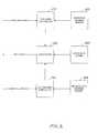
- FIG. 1shows a block diagram of one embodiment of a system configuration in which the teachings of the present invention are implemented.
- the system configuration 100includes a plurality of central processing units (CPUs) 101 a - d, a memory control hub (also referred to as memory control unit) 111 , a P 64 control unit 121 , an Input/Output (IO) control unit 131 , a graphics controller 141 coupled to a graphics subsystem 151 , and a plurality of memory devices 161 .
- CPUscentral processing units
- memory control hubalso referred to as memory control unit
- P 64 control unit 121also referred to as memory control unit
- IOInput/Output
- processorsor “CPU” refers to any machine that is capable of executing a sequence of instructions and shall be taken to include, but not be limited to, general purpose microprocessors, special purpose microprocessors, multi-media controllers and microcontrollers, etc.
- the CPUs 101 a - 101 dare general-purpose microprocessors that are capable of executing an Intel Architecture instruction set.
- the CPUs 101 a - 101 d, the P 64 control unit 121 , the IO control unit 131 , and the AGP graphics control unit 141access the system memory devices 161 via the memory control unit 111 .
- the memory control unit 111in one embodiment, is responsible for servicing all memory transactions that target the system memory devices 161 .
- the memory control unit 111can be a stand-alone unit, an integrated part of a chipset, or a part of some larger unit that control the interfaces between various system components and the system memory devices 161 .
- the P 64 control unit 121provides the interface control between a plurality of PCI- 64 slots 125 and the memory control unit 111 .
- the IO control unit 131provides the interface control between the memory unit 111 and various IO devices and ports including the PCI slots and PCI agents 133 , a plurality of USB ports 135 , a plurality of IDE ports 137 , and other IO devices 139 .
- the AGP graphics control unit 141provides the interface control between the graphics subsystem 151 and the memory control unit 111 . The structure and functions of the memory control unit 111 are described in greater details below.
- FIG. 2shows a block diagram of one embodiment of a memory control configuration according to the teachings of the invention.
- the memory control unit 111includes a memory controller 210 and a translator hub 220 that acts as an interface between the memory controller 210 and the memory devices 161 .
- the memory controller 210is assumed to be a RAMBUS memory controller that operates according to RAMBUS memory control/interface specification and the memory devices 161 are assumed to be SDRAM devices that operate according to SDRAM specification.
- the teachings of the present inventionare not limited to RAMBUS memory controllers and SDRAM devices and can be applied to other memory configurations which utilize memory controllers that operate in accordance with one specification and memory devices that operate according to another specification.
- the translator hub 220translates the RAMBUS control signals and RAMBUS data signals into SDRAM control signals and SDRAM data signals and vice-versa to facilitate data transfer between the memory controller 210 and the memory devices 161 .
- the translator hub 220provides a mechanism for tunneling SDRAM transactions between the RAMBUS memory controller 210 and the SDRAM devices 161 .
- the RAMBUS® memory controllerdefers write data transfers on a write command until the read latency of the RAMBUS type memory device (RDRAM) is met.
- RDRAMRAMBUS type memory device
- This featureallows the RAMBUS memory controller to maintain high bus utilization for RAMBUS type memory devices.
- the deferring of write data transfer by the RAMBUS memory controllerresults in poor bus utilization be cause SDRAM devices require the write data to be sent with the write command.
- This RAMBUS featurethus results in under-utilization of the SDRAM and the RAMBUS memory controller because write commands must be delayed until the write data can be sent from the RAMBUS memory controller to the SDRAM via the translator.
- the present inventionutilizes write buffers to solve this problem and thus improve the data transfer performance between a RAMBUS type memory controller and SDRAM type memory devices.
- the translator hub 220includes a set of write buffers that are used to store write commands and the corresponding write data issued by the memory controller 210 . The buffered write commands are then executed on a first-in-first-out basis.
- the write buffersact as a first-in-first-out queue to control and facilitate data transfer between the RAMBUS memory controller 210 and the SDRAM devices 161 in which new write commands are pushed onto the queue while the oldest write command stored in the write buffers is popped to the SDRAM devices 161 for execution.
- the SDRAM devices 161can start a write operation based upon the buffered write commands when a new write command is received without waiting for the write data for the new write command to be sent from the RAMBUS memory controller 210 .
- the structure and operations of the write buffersare described in more detail below.
- FIG. 3is a block diagram of one embodiment of the translator hub 220 according to the teachings of the present invention.
- the translator hubincludes a channel (also referred to as a main channel herein) that acts as an interface with the RAMUBS memory controller 210 and one or more channels (also referred to as branch channels herein) that act as interface with the SDRAM devices 161 .
- the main channel 310is coupled to receive control signals, data signals, and clock signals from the RAMBUS memory controller 220 and to send the data signals to the RAMBUS memory controller 220 .
- the branch channels 340are coupled to send control, data, and clock signals to the SDRAM devices 161 and to receive data from the SDRAM devices 161 .
- the translator hubfurther includes a decode and SDRAM command generator unit 320 that decodes the commands received from the RAMBUS memory controller 210 via the main channel 310 and generates the appropriate SDRAM commands based upon the decoded commands.
- the SDRAM commands generatedare sent to the SDRAM devices 161 via the branch channels 350 .
- the translator hubalso includes data write buffers 330 to store write data received from the RAMBUS memory controller 210 .
- the buffered write data and the buffered write commandsare sent to the SDRAM devices 161 for execution on a first-in-first-out basis when a new write command is received from the RAMBUS memory controller 210 without waiting for the write data for the new write command.
- the translator hubfurther includes a read data packetizer unit 340 to convert data received from the SDRAM devices 161 via the branch channels 350 into main channel data packets to be sent to the RAMBUS memory controller 210 .
- FIG. 4illustrates a block diagram of one embodiment of the configuration of the write buffers according to the teachings of the present invention.
- the write buffersinclude a row address buffer (also called row address FIFO herein) 410 , a column address buffer (also called column address FIFO herein) 420 , and a write data buffer (also called write data FIFO herein) 430 .
- the row address buffer 410 and column address buffer 420are used to store the row and column addresses associated with the write commands, respectively.
- the write data buffer 430is used to store the write data associated with the write commands.
- the three buffers shown in FIG. 4are configured to function as first-in-first-out queues.
- the row address FIFO 410is advanced with activate memory commands
- the column address FIFO 420is advanced on write commands
- the write data FIFO 430is advanced when the delayed write data is sent.
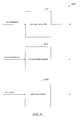
- FIG. 5Ashows a timing diagram of memory utilization without write buffer and FIG. 5B show a timing diagram of memory utilization with write buffer.
- the RAMBUS memory controllere.g., the RAMBUS memory controller 210 shown in FIG. 2 defers write data transfer on a write command until the read latency of a previously issued read command is met, the execution of a write command is delayed by a period corresponding to the read latency of a previous read command.
- a read command 501 Ais sent from the RAMBUS memory controller 210 to the translator hub 220 .
- a read command 505 A(which is the SDRAM read command corresponding to the read command 501 A) is sent from the translator hub 220 to the SDRAM devices 161 .
- the corresponding read data 510 A with respect to the read command 505 Ais transmitted from the SDRAM devices 161 to the translator hub 220 .
- read data 515 A(which is read data 510 A converted into an appropriate format by the translator hub 220 ) is transmitted from the translator hub 220 to the RAMBUS memory controller 210 .
- a write command 520 Ais sent from the RAMBUS memory controller 210 to the translator hub 220 .
- the write data 525 A associated with the write command 520 Ais transmitted from the RAMBUS memory controller 210 to the translator hub 220 .
- the RAMBUS memory controller 210defers write data transfer on a write command until the read latency of a previous read command is met.
- the write data 525 Ais not sent until time T 6 A which is when the read latency with respect to the read command 501 A has been met.
- a write command 530 A(which is the SDRAM write command corresponding to the write command 520 A) is sent to the SDRAM devices 161 from the translator hub 220 .
- write data 535 A(which is write data 525 A converted into an appropriate format by the translator hub 220 ) is transmitted to the SDRAM devices 161 from the translator hub 220 .
- FIG. 5Ait can be seen from FIG. 5A that the delaying of write data transfer by the RAMBUS memory controller 210 , without the use of write buffer according to the teachings of the present invention, results in poor memory bus utilization because there is a large gap (time delay) between the time during which the read data with respect to a read command (e.g., read data 510 A) is transmitted over the SDRAM memory bus and the time during which the write data associated with a write command (e.g., write data 535 A) is transmitted over the SDRAM memory bus.
- FIG. 5Ait can be seen from FIG.
- FIG. 5Bwhich illustrates the memory utilization with write buffers
- the memory utilizationhas been improved significantly because a write command and its corresponding write data stored in the write buffer can be sent to the SDRAM devices 161 for execution when a new write command is received at the translator hub 220 from the RAMBUS memory controller 210 , without waiting for the write data associated with the new write command to arrive from the RAMBUS memory controller 210 .
- a read command 501 Bis sent from the RAMBUS memory controller 210 to the translator hub 220 .
- a read command 505 B(which is the SDRAM read command corresponding to the read command 501 B) is sent from the translator hub 220 to the SDRAM devices 161 .
- the corresponding read data 510 B with respect to the read command 505 Bis transmitted from the SDRAM devices 161 to the translator hub 220 .
- read data 515 B(which is read data 510 B converted into an appropriate format by the translator hub 220 ) is transmitted from the translator hub 220 to the RAMBUS memory controller 210 .
- a new write command 520 Bis sent from the RAMBUS memory controller 210 to the translator hub 220 .
- a previous write command 522 B stored in the write bufferis sent to the SDRAM devices 161 .
- the buffered write data 525 B associated with the write command 522 Bis transmitted to the SDRAM devices on the SDRAM data bus.
- the write data 527 B associated with the new write command 520 Bis transmitted from the RAMBUS memory controller 210 to the translator hub 220 .
- the RAMBUS memory controller 210defers write data transfer on a write command until the read latency of a previous read command is met.
- the write data 527 BAis not sent until time T 7 A which is when the read latency with respect to the read command 501 B has been met.
- the translator hub 220does not need to wait for the write data associated with the new write command to arrive from the RAMBUS memory controller 210 to send a previous write command and its corresponding data stored in the write buffers to the SDRAM devices 161 for execution.
- the previous write data command 522 B and its associated write data 525 B stored in the write buffersare already sent to the SDRAM devices 161 before the new write data 527 B is received from the RAMBUS memory controller 210 .
- the gap (time delay) between the time during which the read data with respect to a read command (e.g., read data 510 B) is transmitted over the SDRAM memory bus and the time during which the write data associated with a write command (e.g., write data 525 B) is transmitted over the SDRAM memory bushas become much smaller.
- the gap (time delay) between the time during which the write data associated with a write command (e.g., write data 527 B) is transmitted over the RAMBUS memory bus and the time during which the read data associated with a subsequent read command (e.g., read data 550 B) is transmitted over the RAMBUS memory bushas become much smaller.
- the use of write bufferssignificantly increases the memory utilization of both the SDRAM devices 161 and the RAMBUS memory controller 210 . This is because a subsequent read after the write does not have to be delayed.
- the write buffers used in the translator hub 220contain data and addresses of pending write operations to the memory devices 161 .
- a problemmay occur if a read command or read memory request is sent to the translator hub 220 to read data from a memory address or location in the memory devices 161 to which one or more pending write commands stored in the buffered are directed. If the read command or read memory request is satisfied by retrieving data from the memory devices 161 , the latest and freshest data will not be used because the corresponding pending write command in the write buffers has not been completed. For example, assuming that the data stored at location XXXX in the memory devices 161 is YYYY at time T 0 .
- a write command and its corresponding data ZZZZare stored in the write buffers to be written to the same memory location XXXX in the memory devices 161 .
- a read commandis sent to the translator hub to read data from the same memory location XXXX from the memory devices 161 .
- the write command stored in the write buffershas not been completed. Therefore the data at location XXXX has not been updated with the latest and freshest data ZZZZ. If the read command is satisfied by retrieving the data from the memory devices 161 , the old data YYYY will be used instead of the freshest and latest data ZZZZ which is still pending in the write buffers.
- the present inventionprovides a mechanism, called read bypass logic or read bypass operation herein, to use the pending write data stored in the write buffers instead of the data stored in the memory devices 161 as read data for a read command that targets the same memory address as one of the pending write commands stored in the write buffers.
- read bypass logicis described in more details below.
- FIG. 6illustrates a block diagram of one embodiment of a read bypass logic/unit implemented within the translator hub 220 according to the teachings of the present invention.
- the read-bypass unitcomprises an address comparison logic to determine whether a read address associated with a read command received from the RAMBUS memory controller 210 matches a write address stored in the write buffers.
- the address comparison logicincludes a row address comparator 630 and a column address comparator 640 . In this embodiment, the address is compared in two parts because the address is sent to the translator hub 220 from the RAMBUS memory controller 210 in two pieces.
- an activate commandprovides the row address portion while a read/write command provides the column address portion.
- the read bypass logicfurther includes a multiplexor 650 to select the corresponding write data the address of which matches the address of the respective read command. In the present embodiment, if the read address matches the write address in the write buffers, the corresponding write data stored in the write buffers will be used as the read data for the respective read command instead of data from the memory devices 161 .
- the write data stored in the write bufferswill be used as read data for the respective read command to ensure that the latest and freshest is obtained since the pending write command has not yet been completed.
- FIG. 7shows a flow diagram of one embodiment of a method 700 according to the teachings of the present invention.
- one or more write commands and their corresponding write dataare received from a first device (e.g., the RAMBUS memory controller 210 ).
- the write data transferis deferred by the first device by a first delay period.
- the first delay periodcorresponds to the read latency of a previous read command.
- the one or more write commandsare stored in a set of buffers.
- a buffered write command and its corresponding write dataare sent to a second device (e.g., the memory devices 161 ) for execution, without waiting for the write data for said another write command to be sent from the first device.
- a new read commandis received from the first device.
- the corresponding write data stored in the buffersis used as read data for the new read command instead of the data stored in the second device.
Landscapes
- Engineering & Computer Science (AREA)
- General Engineering & Computer Science (AREA)
- Theoretical Computer Science (AREA)
- Computer Hardware Design (AREA)
- Physics & Mathematics (AREA)
- General Physics & Mathematics (AREA)
- Memory System (AREA)
Abstract
Description
- The present invention relates to the field of memory control/interface. More specifically, the present invention relates to an apparatus, method, and system for utilizing write buffers to improve the performance of data transfer between a memory controller and memory devices.[0001]
- As computer devices and systems continue to advance and become more complex, effective and efficient management of the interface between different types of devices and components in any given system has become more and more critical in system design and implementation in order to achieve better system performance at component and system levels. With respect to memory control and interface, data transfer between one component (e.g., a processor) and another component (e.g., system memory devices) is typically controlled by a memory controller or a memory control unit that is responsible for servicing memory transactions (e.g., read, write, etc.) that target the system memory devices. Typically, the memory controller and the memory devices operate according to certain data transfer and memory control protocol/specification that is designed to control and service memory transactions between the memory controller and the memory devices. For example, memory transactions that target memory devices such as synchronous dynamic random access memory (SDRAM) devices are controlled by an SDRAM memory controller that operate according to SDRAM specification which includes specification for read, write and other memory operations. To service various types of memory transactions, a typical memory controller generates or issues specific memory commands (e.g., read, write, activate, refresh, etc.) to the memory devices to instruct the memory devices to perform certain operations according to the specific memory commands issued by the memory controller.[0002]
- In certain systems, however, the memory controller used in the systems may be designed by one entity according to a specific specification and the memory devices may be designed by another entity according to a different specification. For example, the memory controller used in a given system may be a RAMBUS® memory controller designed by RAMBUS®, Inc. of Mountain View, Calif., and the memory devices used in the system may be SDRAM devices. In this case, an interface between the memory controller and the memory devices is used to allow the memory controller and the memory devices to communicate and interact with each other. In general, the interface (also called the translator herein) translates the memory commands issued by the memory controller according to one protocol/specification into commands according to another protocol/specification that can be understood by the memory devices. Likewise, the interface or translator receives the data from the memory devices according to the protocol/specification used by the memory devices and transmit the data to the memory controller according to the protocol/specification used by the memory controller. For example, a translator/interface unit can be used to facilitate the data transfer between a RAMBUS® memory controller and SDRAM devices. In this type of configuration, performance may not be optimized due to the different protocols/specifications that are specifically designed for certain types of devices. In other instances, even when a memory controller (e.g., a RAMBUS® memory controller) is designed to work specifically with certain memory devices (e.g., SDRAM devices), certain characteristics associated with the respective components may still cause poor utilization of the memory buses. For example, the RAMBUS® memory controller defers write data transfers on a write command until the read latency of the RAMBUS® type memory device (RDRAM) is met. This feature allows the RAMBUS® memory controller to maintain high bus utilization for RAMBUS® type memory devices. However, in a system in which the RAMBUS® memory controller/interface communicates with SDRAMs via a translator unit, the deferring of write data transfer by the RAMBUS) memory controller results in poor bus utilization because SDRAM devices require the write data to be sent with the write command. This RAMBUS® feature thus results in under-utilization of the SDRAM and the RAMBUS® memory bus because write commands must be delayed until the write data can be sent from the RAMBUS® memory controller to the SDRAM via the translator.[0003]
- The features and advantages of the present invention will be more fully understood by reference to the accompanying drawings, in which:[0004]
- FIG. 1 is a block diagram of one embodiment of a system implementing the teachings of the present invention;[0005]
- FIG. 2 shows a block diagram of one embodiment of a memory controller configuration in which the teachings of the present invention are implemented;[0006]
- FIG. 3 is a block diagram of one embodiment of a translator hub in accordance with the teachings of the present invention;[0007]
- FIG. 4 shows a block diagram of one embodiment of write buffer configuration according to the teachings of the present invention;[0008]
- FIG. 5A shows a timing diagram of memory utilization with no write buffers;[0009]
- FIG. 5B shows a timing diagram of memory utilization with write buffers;[0010]
- FIG. 6 shows a block diagram of one embodiment of read bypass logic in accordance with the teachings of the present invention; and[0011]
- FIG. 7 shows a flow diagram of one embodiment of a method according to the teachings of the present invention.[0012]
- In the following detailed description numerous specific details are set forth in order to provide a thorough understanding of the present invention. However, it will be appreciated by one skilled in the art that the present invention may be understood and practiced without these specific details.[0013]
- In the discussion below, the teachings of the present invention are utilized to implement a method, apparatus, system, and machine-readable medium for utilizing write buffers to improve the performance of data transfer between a memory controller and memory devices. In one embodiment, one or more write commands and their corresponding write data are received from a first device. The corresponding write data may be delayed by the first device by a first delay period. The one or more write commands and their corresponding write data are stored in a set of buffers. Upon another write command is received from the first device, a buffered write command and its corresponding write data are sent to a second device for execution, without waiting for the write data corresponding to said another write command to be sent from the first device. In one embodiment, the first delay period corresponds to a read latency of a previous read command issued by the first device. In one embodiment, the set of buffers includes one or more buffers to store the respective write commands and one or more buffers to store the respective write data. In one embodiment, the one or more buffers to store the respective write commands include a buffer to store row addresses corresponding to the respective write commands and a buffer to store column addresses corresponding to the respective write commands. In one embodiment, the buffered write commands are executed by the second device on a first-in-first-out basis. Upon said another write command is received from the first device, an oldest write command stored in the buffers is popped from the buffers and sent to the second device for execution and said another write command is pushed onto the top of the buffers. In one embodiment, the first device is a memory controller that operates according to a first specification and the second device includes one or more memory devices that operate according to a second specification. In one embodiment, the memory controller is a RAMBUS type memory controller that operates according to RAMBUS memory control specification and the memory devices are synchronous dynamic random access memory (SDRAM) devices that operate according to SDRAM specification. In one embodiment, the SDRAM devices are double data rate synchronous dynamic random access memory (DDR-SDRAM) devices that operate according to DDR-SDRAM specification. The teachings of the present invention are applicable to any scheme, method and system for memory control and interface in computer systems that utilize memory controller(s) according to RAMBUS specification and various types of SDRAM devices according to various types of SDRAM specifications including DDR-SDRAM specification. However, the teachings of the present invention are not limited to RAMBUS type memory controllers and SDRAM type devices and can be applied to any scheme, method, and system of memory control and interface in which a memory controller operates according to one specification and memory devices operate according to another specification. The teachings of the present invention are applicable to any pipelined set of time multiplexed bi-directional buses.[0014]
- FIG. 1 shows a block diagram of one embodiment of a system configuration in which the teachings of the present invention are implemented. The system configuration[0015]100 includes a plurality of central processing units (CPUs)101a-d,a memory control hub (also referred to as memory control unit)111, a
P64 control unit 121, an Input/Output (IO)control unit 131, agraphics controller 141 coupled to agraphics subsystem 151, and a plurality ofmemory devices 161. For the purposes of the present specification, the term “processor” or “CPU” refers to any machine that is capable of executing a sequence of instructions and shall be taken to include, but not be limited to, general purpose microprocessors, special purpose microprocessors, multi-media controllers and microcontrollers, etc. In one embodiment, the CPUs101a-101dare general-purpose microprocessors that are capable of executing an Intel Architecture instruction set. The CPUs101a-101d,theP64 control unit 121, theIO control unit 131, and the AGPgraphics control unit 141 access thesystem memory devices 161 via the memory control unit111. The memory control unit111, in one embodiment, is responsible for servicing all memory transactions that target thesystem memory devices 161. The memory control unit111 can be a stand-alone unit, an integrated part of a chipset, or a part of some larger unit that control the interfaces between various system components and thesystem memory devices 161. TheP64 control unit 121 provides the interface control between a plurality of PCI-64slots 125 and the memory control unit111. TheIO control unit 131 provides the interface control between the memory unit111 and various IO devices and ports including the PCI slots andPCI agents 133, a plurality ofUSB ports 135, a plurality ofIDE ports 137, andother IO devices 139. The AGPgraphics control unit 141 provides the interface control between thegraphics subsystem 151 and the memory control unit111. The structure and functions of the memory control unit111 are described in greater details below. - FIG. 2 shows a block diagram of one embodiment of a memory control configuration according to the teachings of the invention. As shown in FIG. 2, the memory control unit[0016]111 includes a
memory controller 210 and atranslator hub 220 that acts as an interface between thememory controller 210 and thememory devices 161. For explanation and illustration purposes, thememory controller 210 is assumed to be a RAMBUS memory controller that operates according to RAMBUS memory control/interface specification and thememory devices 161 are assumed to be SDRAM devices that operate according to SDRAM specification. It should be recognized by one skilled in the art, however, that the teachings of the present invention are not limited to RAMBUS memory controllers and SDRAM devices and can be applied to other memory configurations which utilize memory controllers that operate in accordance with one specification and memory devices that operate according to another specification. As shown in FIG. 2, thetranslator hub 220 translates the RAMBUS control signals and RAMBUS data signals into SDRAM control signals and SDRAM data signals and vice-versa to facilitate data transfer between thememory controller 210 and thememory devices 161. In other words, thetranslator hub 220 provides a mechanism for tunneling SDRAM transactions between theRAMBUS memory controller 210 and theSDRAM devices 161. As described above, the RAMBUS® memory controller defers write data transfers on a write command until the read latency of the RAMBUS type memory device (RDRAM) is met. This feature allows the RAMBUS memory controller to maintain high bus utilization for RAMBUS type memory devices. However, in a system in which a RAMBUS memory controller/interface communicates with SDRAMs via a translator unit, the deferring of write data transfer by the RAMBUS memory controller results in poor bus utilization be cause SDRAM devices require the write data to be sent with the write command. This RAMBUS feature thus results in under-utilization of the SDRAM and the RAMBUS memory controller because write commands must be delayed until the write data can be sent from the RAMBUS memory controller to the SDRAM via the translator. The present invention utilizes write buffers to solve this problem and thus improve the data transfer performance between a RAMBUS type memory controller and SDRAM type memory devices. In one embodiment, thetranslator hub 220 includes a set of write buffers that are used to store write commands and the corresponding write data issued by thememory controller 210. The buffered write commands are then executed on a first-in-first-out basis. Thus, the write buffers act as a first-in-first-out queue to control and facilitate data transfer between theRAMBUS memory controller 210 and theSDRAM devices 161 in which new write commands are pushed onto the queue while the oldest write command stored in the write buffers is popped to theSDRAM devices 161 for execution. In other words, theSDRAM devices 161 can start a write operation based upon the buffered write commands when a new write command is received without waiting for the write data for the new write command to be sent from theRAMBUS memory controller 210. The structure and operations of the write buffers are described in more detail below. - FIG. 3 is a block diagram of one embodiment of the[0017]
translator hub 220 according to the teachings of the present invention. As shown in FIG. 3, the translator hub includes a channel (also referred to as a main channel herein) that acts as an interface with theRAMUBS memory controller 210 and one or more channels (also referred to as branch channels herein) that act as interface with theSDRAM devices 161. In one embodiment, themain channel 310 is coupled to receive control signals, data signals, and clock signals from theRAMBUS memory controller 220 and to send the data signals to theRAMBUS memory controller 220. In one embodiment, thebranch channels 340 are coupled to send control, data, and clock signals to theSDRAM devices 161 and to receive data from theSDRAM devices 161. The translator hub further includes a decode and SDRAMcommand generator unit 320 that decodes the commands received from theRAMBUS memory controller 210 via themain channel 310 and generates the appropriate SDRAM commands based upon the decoded commands. The SDRAM commands generated are sent to theSDRAM devices 161 via thebranch channels 350. As shown in FIG. 3, the translator hub also includes data writebuffers 330 to store write data received from theRAMBUS memory controller 210. As described herein, the buffered write data and the buffered write commands are sent to theSDRAM devices 161 for execution on a first-in-first-out basis when a new write command is received from theRAMBUS memory controller 210 without waiting for the write data for the new write command. The translator hub further includes a readdata packetizer unit 340 to convert data received from theSDRAM devices 161 via thebranch channels 350 into main channel data packets to be sent to theRAMBUS memory controller 210. - FIG. 4 illustrates a block diagram of one embodiment of the configuration of the write buffers according to the teachings of the present invention. In this embodiment, the write buffers include a row address buffer (also called row address FIFO herein)[0018]410, a column address buffer (also called column address FIFO herein)420, and a write data buffer (also called write data FIFO herein)430. The
row address buffer 410 andcolumn address buffer 420 are used to store the row and column addresses associated with the write commands, respectively. Thewrite data buffer 430 is used to store the write data associated with the write commands. In one embodiment, the three buffers shown in FIG. 4 are configured to function as first-in-first-out queues. In one embodiment, therow address FIFO 410 is advanced with activate memory commands, thecolumn address FIFO 420 is advanced on write commands and thewrite data FIFO 430 is advanced when the delayed write data is sent. - FIG. 5A shows a timing diagram of memory utilization without write buffer and FIG. 5B show a timing diagram of memory utilization with write buffer. As shown in FIG. 5A, because the RAMBUS memory controller (e.g., the[0019]
RAMBUS memory controller 210 shown in FIG. 2) defers write data transfer on a write command until the read latency of a previously issued read command is met, the execution of a write command is delayed by a period corresponding to the read latency of a previous read command. For example, as shown in FIG. 5A, at time T1A, aread command 501A is sent from theRAMBUS memory controller 210 to thetranslator hub 220. At time T2A, a read command505A (which is the SDRAM read command corresponding to the readcommand 501A) is sent from thetranslator hub 220 to theSDRAM devices 161. At time T3A, the corresponding read data510A with respect to the read command505A is transmitted from theSDRAM devices 161 to thetranslator hub 220. At time T4A, readdata 515A (which is read data510A converted into an appropriate format by the translator hub220) is transmitted from thetranslator hub 220 to theRAMBUS memory controller 210. At time T5A, awrite command 520A is sent from theRAMBUS memory controller 210 to thetranslator hub 220. At time T6A, thewrite data 525A associated with thewrite command 520A is transmitted from theRAMBUS memory controller 210 to thetranslator hub 220. Again, theRAMBUS memory controller 210 defers write data transfer on a write command until the read latency of a previous read command is met. In this example, thewrite data 525A is not sent until time T6A which is when the read latency with respect to the readcommand 501A has been met. At time T7A, a write command530A (which is the SDRAM write command corresponding to thewrite command 520A) is sent to theSDRAM devices 161 from thetranslator hub 220. At time T8A, writedata 535A (which is writedata 525A converted into an appropriate format by the translator hub220) is transmitted to theSDRAM devices 161 from thetranslator hub 220. It can be seen from FIG. 5A that the delaying of write data transfer by theRAMBUS memory controller 210, without the use of write buffer according to the teachings of the present invention, results in poor memory bus utilization because there is a large gap (time delay) between the time during which the read data with respect to a read command (e.g., read data510A) is transmitted over the SDRAM memory bus and the time during which the write data associated with a write command (e.g., writedata 535A) is transmitted over the SDRAM memory bus. Similarly, it can be seen from FIG. 5A that there is a large gap (time delay) between the time during which the write data with respect to a write command (e.g., writedata 525A) is transmitted over the RAMBUS memory bus and the time during which the read data associated with a subsequent read command (e.g., read data550A) is transmitted over the RAMBUS memory bus. - Referring to FIG. 5B which illustrates the memory utilization with write buffers, it can be seen that the memory utilization has been improved significantly because a write command and its corresponding write data stored in the write buffer can be sent to the[0020]
SDRAM devices 161 for execution when a new write command is received at thetranslator hub 220 from theRAMBUS memory controller 210, without waiting for the write data associated with the new write command to arrive from theRAMBUS memory controller 210. For example, as shown in FIG. 5B, at time T1A, aread command 501B is sent from theRAMBUS memory controller 210 to thetranslator hub 220. At time T2A, aread command 505B (which is the SDRAM read command corresponding to the readcommand 501B) is sent from thetranslator hub 220 to theSDRAM devices 161. At time T3A, the correspondingread data 510B with respect to the readcommand 505B is transmitted from theSDRAM devices 161 to thetranslator hub 220. At time T4A, readdata 515B (which is readdata 510B converted into an appropriate format by the translator hub220) is transmitted from thetranslator hub 220 to theRAMBUS memory controller 210. At approximately time T4A, a new write command520B is sent from theRAMBUS memory controller 210 to thetranslator hub 220. At time T5A, in response to the new write command520B being received from theRAMBUS memory controller 210, aprevious write command 522B stored in the write buffer is sent to theSDRAM devices 161. At time T6A, the buffered write data525B associated with thewrite command 522B is transmitted to the SDRAM devices on the SDRAM data bus. At time T7A, thewrite data 527B associated with the new write command520B is transmitted from theRAMBUS memory controller 210 to thetranslator hub 220. Again, theRAMBUS memory controller 210 defers write data transfer on a write command until the read latency of a previous read command is met. In this example, the write data527BA is not sent until time T7A which is when the read latency with respect to the readcommand 501B has been met. However, as shown in FIG. 5B, thetranslator hub 220 does not need to wait for the write data associated with the new write command to arrive from theRAMBUS memory controller 210 to send a previous write command and its corresponding data stored in the write buffers to theSDRAM devices 161 for execution. In this example, the previous write data command522B and its associated write data525B stored in the write buffers are already sent to theSDRAM devices 161 before thenew write data 527B is received from theRAMBUS memory controller 210. As a result, the gap (time delay) between the time during which the read data with respect to a read command (e.g., readdata 510B) is transmitted over the SDRAM memory bus and the time during which the write data associated with a write command (e.g., write data525B) is transmitted over the SDRAM memory bus has become much smaller. Similarly, it can be seen from FIG. 5B that the gap (time delay) between the time during which the write data associated with a write command (e.g., writedata 527B) is transmitted over the RAMBUS memory bus and the time during which the read data associated with a subsequent read command (e.g., readdata 550B) is transmitted over the RAMBUS memory bus has become much smaller. Thus, the use of write buffers significantly increases the memory utilization of both theSDRAM devices 161 and theRAMBUS memory controller 210. This is because a subsequent read after the write does not have to be delayed. - As described above, the write buffers used in the[0021]
translator hub 220 contain data and addresses of pending write operations to thememory devices 161. A problem may occur if a read command or read memory request is sent to thetranslator hub 220 to read data from a memory address or location in thememory devices 161 to which one or more pending write commands stored in the buffered are directed. If the read command or read memory request is satisfied by retrieving data from thememory devices 161, the latest and freshest data will not be used because the corresponding pending write command in the write buffers has not been completed. For example, assuming that the data stored at location XXXX in thememory devices 161 is YYYY at time T0. At time T1, a write command and its corresponding data ZZZZ are stored in the write buffers to be written to the same memory location XXXX in thememory devices 161. At time T2, a read command is sent to the translator hub to read data from the same memory location XXXX from thememory devices 161. Assuming that at time T2, the write command stored in the write buffers has not been completed. Therefore the data at location XXXX has not been updated with the latest and freshest data ZZZZ. If the read command is satisfied by retrieving the data from thememory devices 161, the old data YYYY will be used instead of the freshest and latest data ZZZZ which is still pending in the write buffers. To solve this problem, the present invention provides a mechanism, called read bypass logic or read bypass operation herein, to use the pending write data stored in the write buffers instead of the data stored in thememory devices 161 as read data for a read command that targets the same memory address as one of the pending write commands stored in the write buffers. The read bypass logic/operation is described in more details below. - FIG. 6 illustrates a block diagram of one embodiment of a read bypass logic/unit implemented within the[0022]
translator hub 220 according to the teachings of the present invention. In one embodiment, the read-bypass unit comprises an address comparison logic to determine whether a read address associated with a read command received from theRAMBUS memory controller 210 matches a write address stored in the write buffers. In one embodiment, the address comparison logic includes arow address comparator 630 and acolumn address comparator 640. In this embodiment, the address is compared in two parts because the address is sent to thetranslator hub 220 from theRAMBUS memory controller 210 in two pieces. In one embodiment, an activate command provides the row address portion while a read/write command provides the column address portion. In this embodiment, there is a match if both the row address and the column address of the respective read command matches the row address and the column address of one of the write commands stored in the write buffers. The read bypass logic further includes amultiplexor 650 to select the corresponding write data the address of which matches the address of the respective read command. In the present embodiment, if the read address matches the write address in the write buffers, the corresponding write data stored in the write buffers will be used as the read data for the respective read command instead of data from thememory devices 161. Accordingly, if a read command is issued to read data from a memory address for which there is a pending write command in the write buffers, the write data stored in the write buffers will be used as read data for the respective read command to ensure that the latest and freshest is obtained since the pending write command has not yet been completed. - FIG. 7 shows a flow diagram of one embodiment of a[0023]
method 700 according to the teachings of the present invention. Atblock 710, one or more write commands and their corresponding write data are received from a first device (e.g., the RAMBUS memory controller210). The write data transfer is deferred by the first device by a first delay period. In one embodiment, the first delay period corresponds to the read latency of a previous read command. Atblock 720, the one or more write commands are stored in a set of buffers. Atblock 730, upon receiving another write command from the first device, a buffered write command and its corresponding write data are sent to a second device (e.g., the memory devices161) for execution, without waiting for the write data for said another write command to be sent from the first device. Atblock 740, a new read command is received from the first device. Atblock 750, it is determined whether the read address of the new read command matches a write address of a pending write command stored in the buffers. Atblock 760, if there is a match, the corresponding write data stored in the buffers is used as read data for the new read command instead of the data stored in the second device. - The invention has been described in conjunction with the preferred embodiment. It is evident that numerous alternatives, modifications, variations and uses will be apparent to those skilled in the art in light of the foregoing description.[0024]
Claims (30)
1. A method comprising:
receiving one or more write commands and their corresponding write data from a first device, the corresponding write data being delayed by the first device by a first delay period;
storing the one or more write commands and their corresponding write data in a set of buffers; and
upon receiving another write command from the first device, sending a buffered write command and its corresponding write data to a second device for execution, without waiting for the write data corresponding to said another write command to be sent from the first device.
2. The method ofclaim 1 wherein the first delay period corresponds to a read latency of a previous read command.
3. The method ofclaim 1 wherein the buffers comprises a first buffer to store the respective write data, a second buffer to store row addresses corresponding to the respective write commands, and a third buffer to store column addresses corresponding to the respective write commands.
4. The method ofclaim 1 wherein the buffered write commands are executed by the second device on a first-in-first-out basis.
5. The method ofclaim 4 wherein, upon receiving said another write command from the first device, an oldest write command stored in the buffers is popped from the buffers and sent to the second device for execution and said another write command is pushed onto the top of the buffers.
6. The method ofclaim 1 wherein the first device comprises a memory controller and the second device comprises one or more memory devices.
7. The method ofclaim 6 wherein the first device comprises a RAMBUS memory controller that operates according to RAMBUS memory control specification
8. The method ofclaim 6 wherein the second device comprises one or more synchronous dynamic random access memory (SDRAM) devices that operate according to SDRAM specification.
9. The method ofclaim 1 further comprising:
receiving a new read command from the first device;
determining whether a read address associated with the new read command matches a write address associated with a write command stored in the buffers; and
if there is a match, performing a read bypass operation to use the corresponding write data stored in the buffers as read data for the new read command instead of data stored in the second device.
10. The method ofclaim 9 wherein the read address and the write address each comprises a respective row address and a respective column address.
11. The method ofclaim 10 wherein determining comprises:
comparing the row address associated with the new read command to the row address associated with the write command; and
comparing the column address associated with the new read command to the column address associated with the write command.
12. The method ofclaim 9 wherein performing the read bypass operation comprises:
selecting the corresponding write data from the buffers; and
transmitting the corresponding write data to the first device as read data for the new read command.
13. An apparatus comprising:
a set of buffers to store one or more write commands and their corresponding write data received from a first device, the corresponding write data being delayed by the first device by a first delay period, wherein, upon receiving another write command from the first device, a buffered write command and its corresponding data are sent to a second device for execution, without waiting for the write data of said another write command to be sent from the first device.
14. The apparatus ofclaim 13 further comprising:
logic to perform a read bypass operation, comprising:
logic to determine whether a read address associated with a new read command received from the first device matches a write address associated with a write command stored in the buffers; and
logic to use the corresponding write data stored in the buffers as read data for the new read command instead of data stored in the second device if there is a match.
15. The apparatus ofclaim 14 wherein the read address and the write address each comprises a respective row address and a respective column address.
16. The apparatus ofclaim 15 wherein logic to determine comprises:
a first comparator to compare the row address associated with the new read command to the row address associated with the write command; and
a second comparator to compare the column address associated with the new read command to the column address associated with the write command.
17. The apparatus ofclaim 14 wherein logic to perform read bypass operation further comprising:
a multiplexor to select the corresponding write data from the buffers; and
logic to transmit the corresponding write data to the first device as read data for the new read command.
18. The apparatus ofclaim 13 wherein the buffers comprises a first buffer to store the respective write data, a second buffer to store row addresses corresponding to the respective write commands, and a third buffer to store column addresses corresponding to the respective write commands.
19. The apparatus ofclaim 13 wherein, upon receiving said another write command from the first device, an oldest write command stored in the buffers is popped from the buffers and sent to the second device for execution and said another write command is pushed onto the top of the buffers.
20. The apparatus ofclaim 13 wherein the first device comprises a memory controller and the second device comprises one or more memory devices.
21. The apparatus ofclaim 13 wherein the first delay period corresponds to a read latency of a previous read command.
22. A memory control unit comprising:
a first memory controller that issues read and write commands to access a first memory device, the first memory controller deferring write data transfer on a write command for a period corresponding to a read latency of a previously issued read command, the first memory device requiring write data to be sent with a write command to execute a write operation to store the respective write data into the first memory device; and
a translator unit coupled to the first memory controller and the first memory device to provide signal translation between the first memory controller and the first memory device to facilitate memory transactions between the first memory controller and the first memory device, the translator unit including a set of buffers to store one or more write commands and their corresponding write data received from the first memory controller, the translator unit to send a buffered write command and its corresponding write data to the first memory device for execution upon receiving another write command from the first memory controller, without waiting for the write data corresponding to said another write command to be sent from the first memory controller.
23. The memory control unit ofclaim 22 wherein the translator unit further includes logic to perform read bypass operation comprising:
logic to determine whether a read address associated with a new read command received from the first device matches a write address associated with a write command stored in the buffers; and
logic to use the corresponding write data stored in the buffers as read data for the new read command instead of data stored in the second device if there is a match.
24. The memory control unit ofclaim 23 wherein the read address and the write address each comprises a respective row address and a respective column address.
25. The memory control unit ofclaim 24 wherein logic to determine comprises:
a first comparator to compare the row address associated with the new read command to the row address associated with the write command; and
a second comparator to compare the column address associated with the new read command to the column address associated with the write command.
26. The memory control unit ofclaim 24 including:
a multiplexor to select the corresponding write data from the buffers as read data for the new read command.
27. The memory control unit ofclaim 22 wherein the set of buffers comprises:
a first buffer to store write data associated with write commands received from the first memory controller;
a second buffer to store row addresses associated with write commands received from the first memory controller; and
a third buffer to store column addresses associated with write commands received from the first memory controller.
28. A system comprising:
one or more processors;
a system memory; and
a memory control unit coupled to the one or more processors and the system memory, the memory control unit comprising:
a memory controller; and
a translator unit coupled to the memory controller to provide an interface between the memory controller and the system memory, the translator unit comprising:
a set of buffers to store write commands and corresponding write data received from the memory controller in which a buffered write command and its corresponding write data are sent to the system memory for execution upon receiving another write command from the memory controller.
29. The system ofclaim 28 wherein the translator unit further comprises:
read bypass logic comprising:
logic to determine whether a read address associated with a subsequent read command received from the first device matches a write address associated with a write command stored in the buffers; and
logic to use the corresponding write data stored in the buffers as read data for the subsequent read command instead of data stored in the second device if there is a match.
30. The system ofclaim 28 wherein the memory controller defers sending write data associated with a write command for a period corresponding to a read latency of a previously issued read command and wherein the system memory requires that write data associated with a write command be sent with the respective write command to the system memory for the system memory to perform a corresponding write operation.
Priority Applications (2)
| Application Number | Priority Date | Filing Date | Title |
|---|---|---|---|
| US09/749,074US6622227B2 (en) | 2000-12-27 | 2000-12-27 | Method and apparatus for utilizing write buffers in memory control/interface |
| US10/618,885US6901494B2 (en) | 2000-12-27 | 2003-07-14 | Memory control translators |
Applications Claiming Priority (1)
| Application Number | Priority Date | Filing Date | Title |
|---|---|---|---|
| US09/749,074US6622227B2 (en) | 2000-12-27 | 2000-12-27 | Method and apparatus for utilizing write buffers in memory control/interface |
Related Child Applications (1)
| Application Number | Title | Priority Date | Filing Date |
|---|---|---|---|
| US10/618,885DivisionUS6901494B2 (en) | 2000-12-27 | 2003-07-14 | Memory control translators |
Publications (2)
| Publication Number | Publication Date |
|---|---|
| US20020083287A1true US20020083287A1 (en) | 2002-06-27 |
| US6622227B2 US6622227B2 (en) | 2003-09-16 |
Family
ID=25012135
Family Applications (2)
| Application Number | Title | Priority Date | Filing Date |
|---|---|---|---|
| US09/749,074Expired - LifetimeUS6622227B2 (en) | 2000-12-27 | 2000-12-27 | Method and apparatus for utilizing write buffers in memory control/interface |
| US10/618,885Expired - Fee RelatedUS6901494B2 (en) | 2000-12-27 | 2003-07-14 | Memory control translators |
Family Applications After (1)
| Application Number | Title | Priority Date | Filing Date |
|---|---|---|---|
| US10/618,885Expired - Fee RelatedUS6901494B2 (en) | 2000-12-27 | 2003-07-14 | Memory control translators |
Country Status (1)
| Country | Link |
|---|---|
| US (2) | US6622227B2 (en) |
Cited By (14)
| Publication number | Priority date | Publication date | Assignee | Title |
|---|---|---|---|---|
| US20030061447A1 (en)* | 2000-01-05 | 2003-03-27 | Perego Richard E. | Memory system including a point-to-point linked memory subsystem |
| US20040128460A1 (en)* | 1999-12-09 | 2004-07-01 | Rambus Inc. | Transceiver with latency alignment circuitry |
| US20050041504A1 (en)* | 2000-01-05 | 2005-02-24 | Perego Richard E. | Method of operating a memory system including an integrated circuit buffer device |
| US20050166026A1 (en)* | 2000-01-05 | 2005-07-28 | Fred Ware | Configurable width buffered module having switch elements |
| US20050195199A1 (en)* | 2004-03-03 | 2005-09-08 | Anderson Michael H. | Depth buffer for rasterization pipeline |
| US20060168416A1 (en)* | 2003-06-16 | 2006-07-27 | Kessels Jozef Laurentius W | Data processing circuit with multiplexed memory |
| US20070088995A1 (en)* | 2005-09-26 | 2007-04-19 | Rambus Inc. | System including a buffered memory module |
| US7222210B2 (en)* | 2004-03-25 | 2007-05-22 | Micron Technology, Inc. | System and method for memory hub-based expansion bus |
| US7266634B2 (en) | 2000-01-05 | 2007-09-04 | Rambus Inc. | Configurable width buffered module having flyby elements |
| US7356639B2 (en) | 2000-01-05 | 2008-04-08 | Rambus Inc. | Configurable width buffered module having a bypass circuit |
| US7363422B2 (en) | 2000-01-05 | 2008-04-22 | Rambus Inc. | Configurable width buffered module |
| US7562271B2 (en) | 2005-09-26 | 2009-07-14 | Rambus Inc. | Memory system topologies including a buffer device and an integrated circuit memory device |
| US8589643B2 (en) | 2003-10-20 | 2013-11-19 | Round Rock Research, Llc | Arbitration system and method for memory responses in a hub-based memory system |
| US11328764B2 (en) | 2005-09-26 | 2022-05-10 | Rambus Inc. | Memory system topologies including a memory die stack |
Families Citing this family (78)
| Publication number | Priority date | Publication date | Assignee | Title |
|---|---|---|---|---|
| US6791555B1 (en) | 2000-06-23 | 2004-09-14 | Micron Technology, Inc. | Apparatus and method for distributed memory control in a graphics processing system |
| US20030101312A1 (en)* | 2001-11-26 | 2003-05-29 | Doan Trung T. | Machine state storage apparatus and method |
| US7133972B2 (en) | 2002-06-07 | 2006-11-07 | Micron Technology, Inc. | Memory hub with internal cache and/or memory access prediction |
| US7200024B2 (en) | 2002-08-02 | 2007-04-03 | Micron Technology, Inc. | System and method for optically interconnecting memory devices |
| US7117316B2 (en) | 2002-08-05 | 2006-10-03 | Micron Technology, Inc. | Memory hub and access method having internal row caching |
| US7254331B2 (en) | 2002-08-09 | 2007-08-07 | Micron Technology, Inc. | System and method for multiple bit optical data transmission in memory systems |
| US6754117B2 (en) | 2002-08-16 | 2004-06-22 | Micron Technology, Inc. | System and method for self-testing and repair of memory modules |
| US7149874B2 (en) | 2002-08-16 | 2006-12-12 | Micron Technology, Inc. | Memory hub bypass circuit and method |
| US7836252B2 (en) | 2002-08-29 | 2010-11-16 | Micron Technology, Inc. | System and method for optimizing interconnections of memory devices in a multichip module |
| US6820181B2 (en) | 2002-08-29 | 2004-11-16 | Micron Technology, Inc. | Method and system for controlling memory accesses to memory modules having a memory hub architecture |
| US7102907B2 (en) | 2002-09-09 | 2006-09-05 | Micron Technology, Inc. | Wavelength division multiplexed memory module, memory system and method |
| DE10309919B4 (en)* | 2003-03-07 | 2008-09-25 | Qimonda Ag | Buffer block and memory modules |
| US7245145B2 (en) | 2003-06-11 | 2007-07-17 | Micron Technology, Inc. | Memory module and method having improved signal routing topology |
| US7120727B2 (en) | 2003-06-19 | 2006-10-10 | Micron Technology, Inc. | Reconfigurable memory module and method |
| US7260685B2 (en) | 2003-06-20 | 2007-08-21 | Micron Technology, Inc. | Memory hub and access method having internal prefetch buffers |
| US7107415B2 (en) | 2003-06-20 | 2006-09-12 | Micron Technology, Inc. | Posted write buffers and methods of posting write requests in memory modules |
| US7428644B2 (en) | 2003-06-20 | 2008-09-23 | Micron Technology, Inc. | System and method for selective memory module power management |
| US7389364B2 (en) | 2003-07-22 | 2008-06-17 | Micron Technology, Inc. | Apparatus and method for direct memory access in a hub-based memory system |
| US7210059B2 (en) | 2003-08-19 | 2007-04-24 | Micron Technology, Inc. | System and method for on-board diagnostics of memory modules |
| US7133991B2 (en) | 2003-08-20 | 2006-11-07 | Micron Technology, Inc. | Method and system for capturing and bypassing memory transactions in a hub-based memory system |
| US7136958B2 (en) | 2003-08-28 | 2006-11-14 | Micron Technology, Inc. | Multiple processor system and method including multiple memory hub modules |
| US7310752B2 (en) | 2003-09-12 | 2007-12-18 | Micron Technology, Inc. | System and method for on-board timing margin testing of memory modules |
| US7194593B2 (en)* | 2003-09-18 | 2007-03-20 | Micron Technology, Inc. | Memory hub with integrated non-volatile memory |
| US7234070B2 (en) | 2003-10-27 | 2007-06-19 | Micron Technology, Inc. | System and method for using a learning sequence to establish communications on a high-speed nonsynchronous interface in the absence of clock forwarding |
| US7216196B2 (en)* | 2003-12-29 | 2007-05-08 | Micron Technology, Inc. | Memory hub and method for memory system performance monitoring |
| US7330992B2 (en) | 2003-12-29 | 2008-02-12 | Micron Technology, Inc. | System and method for read synchronization of memory modules |
| US7188219B2 (en) | 2004-01-30 | 2007-03-06 | Micron Technology, Inc. | Buffer control system and method for a memory system having outstanding read and write request buffers |
| US7412574B2 (en) | 2004-02-05 | 2008-08-12 | Micron Technology, Inc. | System and method for arbitration of memory responses in a hub-based memory system |
| US7788451B2 (en) | 2004-02-05 | 2010-08-31 | Micron Technology, Inc. | Apparatus and method for data bypass for a bi-directional data bus in a hub-based memory sub-system |
| US7181584B2 (en) | 2004-02-05 | 2007-02-20 | Micron Technology, Inc. | Dynamic command and/or address mirroring system and method for memory modules |
| US7366864B2 (en) | 2004-03-08 | 2008-04-29 | Micron Technology, Inc. | Memory hub architecture having programmable lane widths |
| US7257683B2 (en) | 2004-03-24 | 2007-08-14 | Micron Technology, Inc. | Memory arbitration system and method having an arbitration packet protocol |
| US7213082B2 (en) | 2004-03-29 | 2007-05-01 | Micron Technology, Inc. | Memory hub and method for providing memory sequencing hints |
| US7447240B2 (en) | 2004-03-29 | 2008-11-04 | Micron Technology, Inc. | Method and system for synchronizing communications links in a hub-based memory system |
| US6980042B2 (en) | 2004-04-05 | 2005-12-27 | Micron Technology, Inc. | Delay line synchronizer apparatus and method |
| US7590797B2 (en) | 2004-04-08 | 2009-09-15 | Micron Technology, Inc. | System and method for optimizing interconnections of components in a multichip memory module |
| US7162567B2 (en)* | 2004-05-14 | 2007-01-09 | Micron Technology, Inc. | Memory hub and method for memory sequencing |
| US7222213B2 (en) | 2004-05-17 | 2007-05-22 | Micron Technology, Inc. | System and method for communicating the synchronization status of memory modules during initialization of the memory modules |
| US7363419B2 (en) | 2004-05-28 | 2008-04-22 | Micron Technology, Inc. | Method and system for terminating write commands in a hub-based memory system |
| US7519788B2 (en) | 2004-06-04 | 2009-04-14 | Micron Technology, Inc. | System and method for an asynchronous data buffer having buffer write and read pointers |
| US7310748B2 (en)* | 2004-06-04 | 2007-12-18 | Micron Technology, Inc. | Memory hub tester interface and method for use thereof |
| US7680966B1 (en) | 2004-06-29 | 2010-03-16 | National Semiconductor Corporation | Memory interface including generation of timing signals for memory operation |
| US7296129B2 (en) | 2004-07-30 | 2007-11-13 | International Business Machines Corporation | System, method and storage medium for providing a serialized memory interface with a bus repeater |
| US7392331B2 (en) | 2004-08-31 | 2008-06-24 | Micron Technology, Inc. | System and method for transmitting data packets in a computer system having a memory hub architecture |
| US7331010B2 (en) | 2004-10-29 | 2008-02-12 | International Business Machines Corporation | System, method and storage medium for providing fault detection and correction in a memory subsystem |
| US7512762B2 (en) | 2004-10-29 | 2009-03-31 | International Business Machines Corporation | System, method and storage medium for a memory subsystem with positional read data latency |
| US7305574B2 (en)* | 2004-10-29 | 2007-12-04 | International Business Machines Corporation | System, method and storage medium for bus calibration in a memory subsystem |
| US7299313B2 (en) | 2004-10-29 | 2007-11-20 | International Business Machines Corporation | System, method and storage medium for a memory subsystem command interface |
| US7441060B2 (en) | 2004-10-29 | 2008-10-21 | International Business Machines Corporation | System, method and storage medium for providing a service interface to a memory system |
| US8219745B2 (en)* | 2004-12-02 | 2012-07-10 | International Business Machines Corporation | Memory controller to utilize DRAM write buffers |
| US20060129726A1 (en)* | 2004-12-09 | 2006-06-15 | International Business Machines Corporation | Methods and apparatus for processing a command |
| US7366931B2 (en) | 2004-12-30 | 2008-04-29 | Intel Corporation | Memory modules that receive clock information and are placed in a low power state |
| US7417883B2 (en)* | 2004-12-30 | 2008-08-26 | Intel Corporation | I/O data interconnect reuse as repeater |
| US7992134B2 (en)* | 2005-04-29 | 2011-08-02 | The United States Of America As Represented By The Administrator Of The National Aeronautics And Space Administration | Systems, methods and apparatus for modeling, specifying and deploying policies in autonomous and autonomic systems using agent-oriented software engineering |
| US7478259B2 (en) | 2005-10-31 | 2009-01-13 | International Business Machines Corporation | System, method and storage medium for deriving clocks in a memory system |
| US7747927B2 (en)* | 2005-11-22 | 2010-06-29 | Sandisk Corporation | Method for adapting a memory system to operate with a legacy host originally designed to operate with a different memory system |
| US7739472B2 (en)* | 2005-11-22 | 2010-06-15 | Sandisk Corporation | Memory system for legacy hosts |
| US7685392B2 (en) | 2005-11-28 | 2010-03-23 | International Business Machines Corporation | Providing indeterminate read data latency in a memory system |
| US7636813B2 (en) | 2006-05-22 | 2009-12-22 | International Business Machines Corporation | Systems and methods for providing remote pre-fetch buffers |
| US7640386B2 (en) | 2006-05-24 | 2009-12-29 | International Business Machines Corporation | Systems and methods for providing memory modules with multiple hub devices |
| US7594055B2 (en) | 2006-05-24 | 2009-09-22 | International Business Machines Corporation | Systems and methods for providing distributed technology independent memory controllers |
| US7584336B2 (en)* | 2006-06-08 | 2009-09-01 | International Business Machines Corporation | Systems and methods for providing data modification operations in memory subsystems |
| US7669086B2 (en) | 2006-08-02 | 2010-02-23 | International Business Machines Corporation | Systems and methods for providing collision detection in a memory system |
| US7581073B2 (en) | 2006-08-09 | 2009-08-25 | International Business Machines Corporation | Systems and methods for providing distributed autonomous power management in a memory system |
| US7587559B2 (en) | 2006-08-10 | 2009-09-08 | International Business Machines Corporation | Systems and methods for memory module power management |
| US7539842B2 (en) | 2006-08-15 | 2009-05-26 | International Business Machines Corporation | Computer memory system for selecting memory buses according to physical memory organization information stored in virtual address translation tables |
| US7870459B2 (en)* | 2006-10-23 | 2011-01-11 | International Business Machines Corporation | High density high reliability memory module with power gating and a fault tolerant address and command bus |
| US7721140B2 (en) | 2007-01-02 | 2010-05-18 | International Business Machines Corporation | Systems and methods for improving serviceability of a memory system |
| US7603526B2 (en) | 2007-01-29 | 2009-10-13 | International Business Machines Corporation | Systems and methods for providing dynamic memory pre-fetch |
| US7606988B2 (en) | 2007-01-29 | 2009-10-20 | International Business Machines Corporation | Systems and methods for providing a dynamic memory bank page policy |
| US7554858B2 (en)* | 2007-08-10 | 2009-06-30 | Micron Technology, Inc. | System and method for reducing pin-count of memory devices, and memory device testers for same |
| US9846664B2 (en) | 2010-07-09 | 2017-12-19 | Cypress Semiconductor Corporation | RFID interface and interrupt |
| US8723654B2 (en) | 2010-07-09 | 2014-05-13 | Cypress Semiconductor Corporation | Interrupt generation and acknowledgment for RFID |
| US9092582B2 (en) | 2010-07-09 | 2015-07-28 | Cypress Semiconductor Corporation | Low power, low pin count interface for an RFID transponder |
| US8957763B2 (en) | 2010-07-09 | 2015-02-17 | Cypress Semiconductor Corporation | RFID access method using an indirect memory pointer |
| US8686836B2 (en)* | 2010-07-09 | 2014-04-01 | Cypress Semiconductor Corporation | Fast block write using an indirect memory pointer |
| US9256384B2 (en)* | 2013-02-04 | 2016-02-09 | Avago Technologies General Ip (Singapore) Pte. Ltd. | Method and system for reducing write latency in a data storage system by using a command-push model |
| US10733089B2 (en)* | 2016-07-20 | 2020-08-04 | Micron Technology, Inc. | Apparatuses and methods for write address tracking |
Family Cites Families (8)
| Publication number | Priority date | Publication date | Assignee | Title |
|---|---|---|---|---|
| US4750154A (en)* | 1984-07-10 | 1988-06-07 | Prime Computer, Inc. | Memory alignment system and method |
| US5666494A (en)* | 1995-03-31 | 1997-09-09 | Samsung Electronics Co., Ltd. | Queue management mechanism which allows entries to be processed in any order |
| US6047361A (en)* | 1996-08-21 | 2000-04-04 | International Business Machines Corporation | Memory control device, with a common synchronous interface coupled thereto, for accessing asynchronous memory devices and different synchronous devices |
| WO1999019805A1 (en)* | 1997-10-10 | 1999-04-22 | Rambus Incorporated | Method and apparatus for two step memory write operations |
| US6260127B1 (en)* | 1998-07-13 | 2001-07-10 | Compaq Computer Corporation | Method and apparatus for supporting heterogeneous memory in computer systems |
| US6370073B2 (en)* | 1998-10-01 | 2002-04-09 | Monlithic System Technology, Inc. | Single-port multi-bank memory system having read and write buffers and method of operating same |
| US6449679B2 (en)* | 1999-02-26 | 2002-09-10 | Micron Technology, Inc. | RAM controller interface device for RAM compatibility (memory translator hub) |
| TW525191B (en)* | 2001-09-27 | 2003-03-21 | Leadtek Research Inc | Conversion device of memory instructions and its application system |
- 2000
- 2000-12-27USUS09/749,074patent/US6622227B2/ennot_activeExpired - Lifetime
- 2003
- 2003-07-14USUS10/618,885patent/US6901494B2/ennot_activeExpired - Fee Related
Cited By (65)
| Publication number | Priority date | Publication date | Assignee | Title |
|---|---|---|---|---|
| US7010658B2 (en) | 1999-12-09 | 2006-03-07 | Rambus Inc. | Transceiver with latency alignment circuitry |
| US20040128460A1 (en)* | 1999-12-09 | 2004-07-01 | Rambus Inc. | Transceiver with latency alignment circuitry |
| US8086812B2 (en) | 1999-12-09 | 2011-12-27 | Rambus Inc. | Transceiver with latency alignment circuitry |
| US20070011426A1 (en)* | 1999-12-09 | 2007-01-11 | Rambus Inc. | Transceiver with latency alignment circuitry |
| US7124270B2 (en) | 1999-12-09 | 2006-10-17 | Rambus Inc. | Transceiver with latency alignment circuitry |
| US20050160247A1 (en)* | 1999-12-09 | 2005-07-21 | Dillon John B. | Transceiver with latency alignment circuitry |
| US7065622B2 (en) | 1999-12-09 | 2006-06-20 | Rambus Inc. | Transceiver with latency alignment circuitry |
| US7363422B2 (en) | 2000-01-05 | 2008-04-22 | Rambus Inc. | Configurable width buffered module |
| US20050156934A1 (en)* | 2000-01-05 | 2005-07-21 | Perego Richard E. | System featuring memory modules that include an integrated circuit buffer devices |
| US20050210196A1 (en)* | 2000-01-05 | 2005-09-22 | Perego Richard E | Memory module having an integrated circuit buffer device |
| US20050207255A1 (en)* | 2000-01-05 | 2005-09-22 | Perego Richard E | System having a controller device, a buffer device and a plurality of memory devices |
| US20050223179A1 (en)* | 2000-01-05 | 2005-10-06 | Perego Richard E | Buffer device and method of operation in a buffer device |
| US7000062B2 (en) | 2000-01-05 | 2006-02-14 | Rambus Inc. | System and method featuring a controller device and a memory module that includes an integrated circuit buffer device and a plurality of integrated circuit memory devices |
| US7003618B2 (en) | 2000-01-05 | 2006-02-21 | Rambus Inc. | System featuring memory modules that include an integrated circuit buffer devices |
| US20050193163A1 (en)* | 2000-01-05 | 2005-09-01 | Perego Richard E. | Integrated circuit buffer device |
| US7010642B2 (en) | 2000-01-05 | 2006-03-07 | Rambus Inc. | System featuring a controller device and a memory module that includes an integrated circuit buffer device and a plurality of integrated circuit memory devices |
| US7017002B2 (en) | 2000-01-05 | 2006-03-21 | Rambus, Inc. | System featuring a master device, a buffer device and a plurality of integrated circuit memory devices |
| US20060067141A1 (en)* | 2000-01-05 | 2006-03-30 | Perego Richard E | Integrated circuit buffer device |
| US7051151B2 (en) | 2000-01-05 | 2006-05-23 | Rambus Inc. | Integrated circuit buffer device |
| US7062597B2 (en) | 2000-01-05 | 2006-06-13 | Rambus Inc. | Integrated circuit buffer device |
| US20050166026A1 (en)* | 2000-01-05 | 2005-07-28 | Fred Ware | Configurable width buffered module having switch elements |
| US7206896B2 (en) | 2000-01-05 | 2007-04-17 | Rambus Inc. | Integrated circuit buffer device |
| US20090319719A1 (en)* | 2000-01-05 | 2009-12-24 | Rambus Inc. | System Having A Controller Device, A Buffer Device And A Plurality Of Memory Devices |
| US20050149662A1 (en)* | 2000-01-05 | 2005-07-07 | Perego Richard E. | System having a plurality of integrated circuit buffer devices |
| US7200710B2 (en) | 2000-01-05 | 2007-04-03 | Rambus Inc. | Buffer device and method of operation in a buffer device |
| US7526597B2 (en) | 2000-01-05 | 2009-04-28 | Rambus Inc. | Buffered memory having a control bus and dedicated data lines |
| US7206897B2 (en) | 2000-01-05 | 2007-04-17 | Rambus Inc. | Memory module having an integrated circuit buffer device |
| US20050041504A1 (en)* | 2000-01-05 | 2005-02-24 | Perego Richard E. | Method of operating a memory system including an integrated circuit buffer device |
| US7404032B2 (en) | 2000-01-05 | 2008-07-22 | Rambus Inc. | Configurable width buffered module having switch elements |
| US7266634B2 (en) | 2000-01-05 | 2007-09-04 | Rambus Inc. | Configurable width buffered module having flyby elements |
| US7320047B2 (en) | 2000-01-05 | 2008-01-15 | Rambus Inc. | System having a controller device, a buffer device and a plurality of memory devices |
| US7356639B2 (en) | 2000-01-05 | 2008-04-08 | Rambus Inc. | Configurable width buffered module having a bypass circuit |
| US20030061447A1 (en)* | 2000-01-05 | 2003-03-27 | Perego Richard E. | Memory system including a point-to-point linked memory subsystem |
| US8473706B2 (en) | 2003-06-16 | 2013-06-25 | Callahan Cellular L.L.C. | Data processing circuit with multiplexed memory |
| US8190829B2 (en) | 2003-06-16 | 2012-05-29 | Callahan Cellular L.L.C. | Data processing circuit with multiplexed memory |
| US7487300B2 (en)* | 2003-06-16 | 2009-02-03 | Nxp B.V. | Data processing circuit with multiplexed memory |
| US20060168416A1 (en)* | 2003-06-16 | 2006-07-27 | Kessels Jozef Laurentius W | Data processing circuit with multiplexed memory |
| US20090106520A1 (en)* | 2003-06-16 | 2009-04-23 | Nxp B.V. | Data processing circuit with multiplexed memory |
| US8589643B2 (en) | 2003-10-20 | 2013-11-19 | Round Rock Research, Llc | Arbitration system and method for memory responses in a hub-based memory system |
| US20050195199A1 (en)* | 2004-03-03 | 2005-09-08 | Anderson Michael H. | Depth buffer for rasterization pipeline |
| US8081182B2 (en)* | 2004-03-03 | 2011-12-20 | Qualcomm Incorporated | Depth buffer for rasterization pipeline |
| US7222210B2 (en)* | 2004-03-25 | 2007-05-22 | Micron Technology, Inc. | System and method for memory hub-based expansion bus |
| US8019924B2 (en) | 2004-03-25 | 2011-09-13 | Round Rock Research, Llc | System and method for memory hub-based expansion bus |
| US8117371B2 (en) | 2004-03-25 | 2012-02-14 | Round Rock Research, Llc | System and method for memory hub-based expansion bus |
| US7899969B2 (en) | 2004-03-25 | 2011-03-01 | Round Rock Research, Llc | System and method for memory hub-based expansion bus |
| US20110145463A1 (en)* | 2004-03-25 | 2011-06-16 | Round Rock Research, Llc | System and method for memory hub-based expansion bus |
| US7685364B2 (en) | 2005-09-26 | 2010-03-23 | Rambus Inc. | Memory system topologies including a buffer device and an integrated circuit memory device |
| US9117035B2 (en) | 2005-09-26 | 2015-08-25 | Rambus Inc. | Memory system topologies including a buffer device and an integrated circuit memory device |
| US7562271B2 (en) | 2005-09-26 | 2009-07-14 | Rambus Inc. | Memory system topologies including a buffer device and an integrated circuit memory device |
| US8108607B2 (en) | 2005-09-26 | 2012-01-31 | Rambus Inc. | Memory system topologies including a buffer device and an integrated circuit memory device |
| US20100146199A1 (en)* | 2005-09-26 | 2010-06-10 | Rambus Inc. | Memory System Topologies Including A Buffer Device And An Integrated Circuit Memory Device |
| US7729151B2 (en) | 2005-09-26 | 2010-06-01 | Rambus Inc. | System including a buffered memory module |
| US7464225B2 (en) | 2005-09-26 | 2008-12-09 | Rambus Inc. | Memory module including a plurality of integrated circuit memory devices and a plurality of buffer devices in a matrix topology |
| US9865329B2 (en) | 2005-09-26 | 2018-01-09 | Rambus Inc. | Memory system topologies including a buffer device and an integrated circuit memory device |
| US20070088995A1 (en)* | 2005-09-26 | 2007-04-19 | Rambus Inc. | System including a buffered memory module |
| US20090198924A1 (en)* | 2005-09-26 | 2009-08-06 | Rambus Inc. | Memory System Topologies Including A Buffer Device And An Integrated Circuit Memory Device |
| US9563583B2 (en) | 2005-09-26 | 2017-02-07 | Rambus Inc. | Memory system topologies including a buffer device and an integrated circuit memory device |
| US8539152B2 (en) | 2005-09-26 | 2013-09-17 | Rambus Inc. | Memory system topologies including a buffer device and an integrated circuit memory device |
| US10381067B2 (en) | 2005-09-26 | 2019-08-13 | Rambus Inc. | Memory system topologies including a buffer device and an integrated circuit memory device |
| US10535398B2 (en) | 2005-09-26 | 2020-01-14 | Rambus Inc. | Memory system topologies including a buffer device and an integrated circuit memory device |
| US10672458B1 (en) | 2005-09-26 | 2020-06-02 | Rambus Inc. | Memory system topologies including a buffer device and an integrated circuit memory device |
| US11043258B2 (en) | 2005-09-26 | 2021-06-22 | Rambus Inc. | Memory system topologies including a memory die stack |
| US11328764B2 (en) | 2005-09-26 | 2022-05-10 | Rambus Inc. | Memory system topologies including a memory die stack |
| US11727982B2 (en) | 2005-09-26 | 2023-08-15 | Rambus Inc. | Memory system topologies including a memory die stack |
| US12394471B2 (en) | 2005-09-26 | 2025-08-19 | Rambus Inc. | Memory system topologies including a memory die stack |
Also Published As
| Publication number | Publication date |
|---|---|
| US6622227B2 (en) | 2003-09-16 |
| US6901494B2 (en) | 2005-05-31 |
| US20040015650A1 (en) | 2004-01-22 |
Similar Documents
| Publication | Publication Date | Title |
|---|---|---|
| US6622227B2 (en) | Method and apparatus for utilizing write buffers in memory control/interface | |
| US6212611B1 (en) | Method and apparatus for providing a pipelined memory controller | |
| US6026464A (en) | Memory control system and method utilizing distributed memory controllers for multibank memory | |
| US5544346A (en) | System having a bus interface unit for overriding a normal arbitration scheme after a system resource device has already gained control of a bus | |
| KR100296633B1 (en) | Dynamic deferred transaction mechanism | |
| CN114490460B (en) | FLASH controller for ASIC and control method thereof | |
| US6151651A (en) | Communication link with isochronous and asynchronous priority modes coupling bridge circuits in a computer system | |
| US7644207B2 (en) | High speed bus for isolated data acquisition applications | |
| CN101021820A (en) | Data transmission and reception method and system capable of reducing delay | |
| KR920006851A (en) | Data processing system and method | |
| JPH0332094B2 (en) | ||
| KR20070049676A (en) | Method and apparatus for sending memory pre-fetch commands over a bus | |
| US20110153875A1 (en) | Opportunistic dma header insertion | |
| US5519872A (en) | Fast address latch with automatic address incrementing | |
| KR100881049B1 (en) | Multiple address two channel bus structure | |
| US6301629B1 (en) | High speed/low speed interface with prediction cache | |
| US9342474B2 (en) | Switching a computer system from a high performance mode to a low power mode | |
| US6044474A (en) | Memory controller with buffered CAS/RAS external synchronization capability for reducing the effects of clock-to-signal skew | |
| US7913013B2 (en) | Semiconductor integrated circuit | |
| US5913231A (en) | Method and system for high speed memory address forwarding mechanism | |
| US20040186941A1 (en) | Link bus between control chipsets and arbitration method thereof | |
| US5799161A (en) | Method and apparatus for concurrent data routing | |
| US7779188B2 (en) | System and method to reduce memory latency in microprocessor systems connected with a bus | |
| US20030084223A1 (en) | Bus to system memory delayed read processing | |
| US6748513B1 (en) | Method and apparatus for a low latency source-synchronous address receiver for a host system bus in a memory controller |
Legal Events
| Date | Code | Title | Description |
|---|---|---|---|
| AS | Assignment | Owner name:INTEL CORPORATION, CALIFORNIA Free format text:ASSIGNMENT OF ASSIGNORS INTEREST;ASSIGNORS:ZUMKEHR, JOHN F.;VOGT, PETE D.;REEL/FRAME:011716/0370;SIGNING DATES FROM 20010405 TO 20010406 | |
| STCF | Information on status: patent grant | Free format text:PATENTED CASE | |
| FEPP | Fee payment procedure | Free format text:PAYOR NUMBER ASSIGNED (ORIGINAL EVENT CODE: ASPN); ENTITY STATUS OF PATENT OWNER: LARGE ENTITY | |
| FPAY | Fee payment | Year of fee payment:4 | |
| FPAY | Fee payment | Year of fee payment:8 | |
| FPAY | Fee payment | Year of fee payment:12 |