US20020081823A1 - Generic layer transfer methodology by controlled cleavage process - Google Patents
Generic layer transfer methodology by controlled cleavage processDownload PDFInfo
- Publication number
- US20020081823A1 US20020081823A1US10/090,704US9070402AUS2002081823A1US 20020081823 A1US20020081823 A1US 20020081823A1US 9070402 AUS9070402 AUS 9070402AUS 2002081823 A1US2002081823 A1US 2002081823A1
- Authority
- US
- United States
- Prior art keywords
- substrate
- energy
- cleave
- wafer
- region
- Prior art date
- Legal status (The legal status is an assumption and is not a legal conclusion. Google has not performed a legal analysis and makes no representation as to the accuracy of the status listed.)
- Abandoned
Links
- 238000000034methodMethods0.000titleclaimsabstractdescription142
- 230000008569processEffects0.000titleclaimsdescription74
- 238000012546transferMethods0.000titledescription10
- 238000003776cleavage reactionMethods0.000titledescription2
- 230000007017scissionEffects0.000titledescription2
- 239000000758substrateSubstances0.000claimsabstractdescription224
- 239000000463materialSubstances0.000claimsabstractdescription132
- 230000009471actionEffects0.000claimsabstractdescription57
- 239000002245particleSubstances0.000claimsdescription43
- 230000001902propagating effectEffects0.000claimsdescription5
- 230000003313weakening effectEffects0.000claimsdescription2
- 238000006467substitution reactionMethods0.000claims1
- 235000012431wafersNutrition0.000description95
- XUIMIQQOPSSXEZ-UHFFFAOYSA-NSiliconChemical compound[Si]XUIMIQQOPSSXEZ-UHFFFAOYSA-N0.000description44
- 229910052710siliconInorganic materials0.000description44
- 239000010703siliconSubstances0.000description44
- 239000012530fluidSubstances0.000description36
- 239000010408filmSubstances0.000description33
- VYPSYNLAJGMNEJ-UHFFFAOYSA-Nsilicon dioxideInorganic materialsO=[Si]=OVYPSYNLAJGMNEJ-UHFFFAOYSA-N0.000description27
- 239000010409thin filmSubstances0.000description26
- 238000010586diagramMethods0.000description22
- 239000007789gasSubstances0.000description22
- 239000010410layerSubstances0.000description22
- 230000000977initiatory effectEffects0.000description18
- 239000007788liquidSubstances0.000description18
- 239000011521glassSubstances0.000description15
- 238000002513implantationMethods0.000description15
- 239000000126substanceSubstances0.000description14
- 239000012212insulatorSubstances0.000description13
- 150000002500ionsChemical class0.000description11
- 239000000377silicon dioxideSubstances0.000description11
- 235000012239silicon dioxideNutrition0.000description10
- 239000001257hydrogenSubstances0.000description9
- 229910052739hydrogenInorganic materials0.000description9
- 238000004519manufacturing processMethods0.000description9
- 230000015572biosynthetic processEffects0.000description8
- 238000012545processingMethods0.000description8
- 239000004065semiconductorSubstances0.000description8
- UFHFLCQGNIYNRP-UHFFFAOYSA-NHydrogenChemical compound[H][H]UFHFLCQGNIYNRP-UHFFFAOYSA-N0.000description7
- 238000005520cutting processMethods0.000description7
- 230000007547defectEffects0.000description7
- 239000010432diamondSubstances0.000description7
- 238000005468ion implantationMethods0.000description7
- 238000005498polishingMethods0.000description7
- 229910003460diamondInorganic materials0.000description6
- -1gasesChemical class0.000description6
- 239000007943implantSubstances0.000description6
- 230000001965increasing effectEffects0.000description6
- 241000894007speciesSpecies0.000description6
- 229910052581Si3N4Inorganic materials0.000description5
- 239000000853adhesiveSubstances0.000description5
- 230000001070adhesive effectEffects0.000description5
- 239000003989dielectric materialSubstances0.000description5
- 238000007654immersionMethods0.000description5
- 238000005304joiningMethods0.000description5
- HQVNEWCFYHHQES-UHFFFAOYSA-Nsilicon nitrideChemical compoundN12[Si]34N5[Si]62N3[Si]51N64HQVNEWCFYHHQES-UHFFFAOYSA-N0.000description5
- 239000002210silicon-based materialSubstances0.000description5
- 125000004429atomChemical group0.000description4
- 230000008901benefitEffects0.000description4
- 238000004140cleaningMethods0.000description4
- 229910052681coesiteInorganic materials0.000description4
- 150000001875compoundsChemical class0.000description4
- 238000001816coolingMethods0.000description4
- 229910052906cristobaliteInorganic materials0.000description4
- 238000009792diffusion processMethods0.000description4
- 229910052751metalInorganic materials0.000description4
- 239000002184metalSubstances0.000description4
- VNWKTOKETHGBQD-UHFFFAOYSA-NmethaneChemical compoundCVNWKTOKETHGBQD-UHFFFAOYSA-N0.000description4
- 239000000203mixtureSubstances0.000description4
- 230000007935neutral effectEffects0.000description4
- 230000003647oxidationEffects0.000description4
- 238000007254oxidation reactionMethods0.000description4
- 239000002002slurrySubstances0.000description4
- 229910052682stishoviteInorganic materials0.000description4
- 238000007669thermal treatmentMethods0.000description4
- 229910052905tridymiteInorganic materials0.000description4
- XLYOFNOQVPJJNP-UHFFFAOYSA-NwaterChemical compoundOXLYOFNOQVPJJNP-UHFFFAOYSA-N0.000description4
- 239000004642PolyimideSubstances0.000description3
- ATJFFYVFTNAWJD-UHFFFAOYSA-NTinChemical compound[Sn]ATJFFYVFTNAWJD-UHFFFAOYSA-N0.000description3
- 238000000137annealingMethods0.000description3
- 239000013590bulk materialSubstances0.000description3
- 238000006243chemical reactionMethods0.000description3
- 239000004020conductorSubstances0.000description3
- 238000005336crackingMethods0.000description3
- 238000005485electric heatingMethods0.000description3
- 230000005672electromagnetic fieldEffects0.000description3
- 238000010894electron beam technologyMethods0.000description3
- 230000000670limiting effectEffects0.000description3
- 229910052754neonInorganic materials0.000description3
- GKAOGPIIYCISHV-UHFFFAOYSA-Nneon atomChemical compound[Ne]GKAOGPIIYCISHV-UHFFFAOYSA-N0.000description3
- 230000001590oxidative effectEffects0.000description3
- 239000004033plasticSubstances0.000description3
- 229920003023plasticPolymers0.000description3
- 238000007517polishing processMethods0.000description3
- 229910021420polycrystalline siliconInorganic materials0.000description3
- 229920001721polyimidePolymers0.000description3
- 229920005591polysiliconPolymers0.000description3
- 239000010453quartzSubstances0.000description3
- 230000005855radiationEffects0.000description3
- 238000000926separation methodMethods0.000description3
- HBMJWWWQQXIZIP-UHFFFAOYSA-Nsilicon carbideChemical compound[Si+]#[C-]HBMJWWWQQXIZIP-UHFFFAOYSA-N0.000description3
- 229910010271silicon carbideInorganic materials0.000description3
- 239000013526supercooled liquidSubstances0.000description3
- 230000003746surface roughnessEffects0.000description3
- QGZKDVFQNNGYKY-UHFFFAOYSA-NAmmoniaChemical compoundNQGZKDVFQNNGYKY-UHFFFAOYSA-N0.000description2
- XKRFYHLGVUSROY-UHFFFAOYSA-NArgonChemical compound[Ar]XKRFYHLGVUSROY-UHFFFAOYSA-N0.000description2
- GWEVSGVZZGPLCZ-UHFFFAOYSA-NTitan oxideChemical compoundO=[Ti]=OGWEVSGVZZGPLCZ-UHFFFAOYSA-N0.000description2
- 238000005275alloyingMethods0.000description2
- 238000013459approachMethods0.000description2
- 239000012809cooling fluidSubstances0.000description2
- 239000013078crystalSubstances0.000description2
- 238000009826distributionMethods0.000description2
- 238000000227grindingMethods0.000description2
- 239000001307heliumSubstances0.000description2
- 229910052734heliumInorganic materials0.000description2
- SWQJXJOGLNCZEY-UHFFFAOYSA-Nhelium atomChemical compound[He]SWQJXJOGLNCZEY-UHFFFAOYSA-N0.000description2
- 150000002431hydrogenChemical class0.000description2
- 150000002483hydrogen compoundsChemical class0.000description2
- VCJMYUPGQJHHFU-UHFFFAOYSA-Niron(3+);trinitrateChemical compound[Fe+3].[O-][N+]([O-])=O.[O-][N+]([O-])=O.[O-][N+]([O-])=OVCJMYUPGQJHHFU-UHFFFAOYSA-N0.000description2
- 238000002955isolationMethods0.000description2
- 230000007246mechanismEffects0.000description2
- 238000012986modificationMethods0.000description2
- 230000004048modificationEffects0.000description2
- 239000007800oxidant agentSubstances0.000description2
- 238000009832plasma treatmentMethods0.000description2
- 229910052594sapphireInorganic materials0.000description2
- 239000010980sapphireSubstances0.000description2
- 239000003351stiffenerSubstances0.000description2
- 230000008685targetingEffects0.000description2
- PNEYBMLMFCGWSK-UHFFFAOYSA-NAluminaChemical compound[O-2].[O-2].[O-2].[Al+3].[Al+3]PNEYBMLMFCGWSK-UHFFFAOYSA-N0.000description1
- JBRZTFJDHDCESZ-UHFFFAOYSA-NAsGaChemical compound[As]#[Ga]JBRZTFJDHDCESZ-UHFFFAOYSA-N0.000description1
- OKTJSMMVPCPJKN-UHFFFAOYSA-NCarbonChemical compound[C]OKTJSMMVPCPJKN-UHFFFAOYSA-N0.000description1
- 241001050985DiscoSpecies0.000description1
- 239000004593EpoxySubstances0.000description1
- 229910001218Gallium arsenideInorganic materials0.000description1
- JMASRVWKEDWRBT-UHFFFAOYSA-NGallium nitrideChemical compound[Ga]#NJMASRVWKEDWRBT-UHFFFAOYSA-N0.000description1
- NRTOMJZYCJJWKI-UHFFFAOYSA-NTitanium nitrideChemical compound[Ti]#NNRTOMJZYCJJWKI-UHFFFAOYSA-N0.000description1
- 239000003082abrasive agentSubstances0.000description1
- 239000002253acidSubstances0.000description1
- 230000002378acidificating effectEffects0.000description1
- 230000003213activating effectEffects0.000description1
- 239000005456alcohol based solventSubstances0.000description1
- 229910021529ammoniaInorganic materials0.000description1
- 229910052786argonInorganic materials0.000description1
- 230000000712assemblyEffects0.000description1
- 238000000429assemblyMethods0.000description1
- 239000012298atmosphereSubstances0.000description1
- QVGXLLKOCUKJST-UHFFFAOYSA-Natomic oxygenChemical compound[O]QVGXLLKOCUKJST-UHFFFAOYSA-N0.000description1
- 239000005388borosilicate glassSubstances0.000description1
- 229910010293ceramic materialInorganic materials0.000description1
- 229910000420cerium oxideInorganic materials0.000description1
- 238000005229chemical vapour depositionMethods0.000description1
- 239000008119colloidal silicaSubstances0.000description1
- 238000010276constructionMethods0.000description1
- 239000002826coolantSubstances0.000description1
- 239000008367deionised waterSubstances0.000description1
- 229910021641deionized waterInorganic materials0.000description1
- 230000032798delaminationEffects0.000description1
- 230000000694effectsEffects0.000description1
- 230000003028elevating effectEffects0.000description1
- 238000005516engineering processMethods0.000description1
- 230000005669field effectEffects0.000description1
- 238000007730finishing processMethods0.000description1
- 229910002804graphiteInorganic materials0.000description1
- 239000010439graphiteSubstances0.000description1
- 238000010438heat treatmentMethods0.000description1
- MVFCKEFYUDZOCX-UHFFFAOYSA-Niron(2+);dinitrateChemical compound[Fe+2].[O-][N+]([O-])=O.[O-][N+]([O-])=OMVFCKEFYUDZOCX-UHFFFAOYSA-N0.000description1
- 230000006911nucleationEffects0.000description1
- 238000010899nucleationMethods0.000description1
- TWNQGVIAIRXVLR-UHFFFAOYSA-Noxo(oxoalumanyloxy)alumaneChemical compoundO=[Al]O[Al]=OTWNQGVIAIRXVLR-UHFFFAOYSA-N0.000description1
- BMMGVYCKOGBVEV-UHFFFAOYSA-Noxo(oxoceriooxy)ceriumChemical compound[Ce]=O.O=[Ce]=OBMMGVYCKOGBVEV-UHFFFAOYSA-N0.000description1
- 239000001301oxygenSubstances0.000description1
- 229910052760oxygenInorganic materials0.000description1
- 238000004806packaging method and processMethods0.000description1
- 229920000642polymerPolymers0.000description1
- 239000004814polyurethaneSubstances0.000description1
- 229920002635polyurethanePolymers0.000description1
- 238000002360preparation methodMethods0.000description1
- 238000004151rapid thermal annealingMethods0.000description1
- 230000002829reductive effectEffects0.000description1
- 230000002441reversible effectEffects0.000description1
- 238000012552reviewMethods0.000description1
- 150000004760silicatesChemical class0.000description1
- 229910052814silicon oxideInorganic materials0.000description1
- 230000003068static effectEffects0.000description1
- 238000005728strengtheningMethods0.000description1
- 230000000153supplemental effectEffects0.000description1
- 239000002344surface layerSubstances0.000description1
- 239000004094surface-active agentSubstances0.000description1
- 230000002459sustained effectEffects0.000description1
- 239000004408titanium dioxideSubstances0.000description1
- 238000011282treatmentMethods0.000description1
Images


Classifications
- H—ELECTRICITY
- H01—ELECTRIC ELEMENTS
- H01L—SEMICONDUCTOR DEVICES NOT COVERED BY CLASS H10
- H01L21/00—Processes or apparatus adapted for the manufacture or treatment of semiconductor or solid state devices or of parts thereof
- H01L21/70—Manufacture or treatment of devices consisting of a plurality of solid state components formed in or on a common substrate or of parts thereof; Manufacture of integrated circuit devices or of parts thereof
- H01L21/71—Manufacture of specific parts of devices defined in group H01L21/70
- H01L21/76—Making of isolation regions between components
- H01L21/762—Dielectric regions, e.g. EPIC dielectric isolation, LOCOS; Trench refilling techniques, SOI technology, use of channel stoppers
- H01L21/7624—Dielectric regions, e.g. EPIC dielectric isolation, LOCOS; Trench refilling techniques, SOI technology, use of channel stoppers using semiconductor on insulator [SOI] technology
- H01L21/76251—Dielectric regions, e.g. EPIC dielectric isolation, LOCOS; Trench refilling techniques, SOI technology, use of channel stoppers using semiconductor on insulator [SOI] technology using bonding techniques
- H01L21/76254—Dielectric regions, e.g. EPIC dielectric isolation, LOCOS; Trench refilling techniques, SOI technology, use of channel stoppers using semiconductor on insulator [SOI] technology using bonding techniques with separation/delamination along an ion implanted layer, e.g. Smart-cut, Unibond
- H—ELECTRICITY
- H01—ELECTRIC ELEMENTS
- H01L—SEMICONDUCTOR DEVICES NOT COVERED BY CLASS H10
- H01L21/00—Processes or apparatus adapted for the manufacture or treatment of semiconductor or solid state devices or of parts thereof
- H01L21/02—Manufacture or treatment of semiconductor devices or of parts thereof
- H01L21/04—Manufacture or treatment of semiconductor devices or of parts thereof the devices having potential barriers, e.g. a PN junction, depletion layer or carrier concentration layer
- H01L21/18—Manufacture or treatment of semiconductor devices or of parts thereof the devices having potential barriers, e.g. a PN junction, depletion layer or carrier concentration layer the devices having semiconductor bodies comprising elements of Group IV of the Periodic Table or AIIIBV compounds with or without impurities, e.g. doping materials
- H01L21/185—Joining of semiconductor bodies for junction formation
- H01L21/187—Joining of semiconductor bodies for junction formation by direct bonding
- B—PERFORMING OPERATIONS; TRANSPORTING
- B81—MICROSTRUCTURAL TECHNOLOGY
- B81C—PROCESSES OR APPARATUS SPECIALLY ADAPTED FOR THE MANUFACTURE OR TREATMENT OF MICROSTRUCTURAL DEVICES OR SYSTEMS
- B81C1/00—Manufacture or treatment of devices or systems in or on a substrate
- B81C1/00349—Creating layers of material on a substrate
- B81C1/0038—Processes for creating layers of materials not provided for in groups B81C1/00357 - B81C1/00373
- H—ELECTRICITY
- H01—ELECTRIC ELEMENTS
- H01L—SEMICONDUCTOR DEVICES NOT COVERED BY CLASS H10
- H01L21/00—Processes or apparatus adapted for the manufacture or treatment of semiconductor or solid state devices or of parts thereof
- H01L21/02—Manufacture or treatment of semiconductor devices or of parts thereof
- H01L21/02104—Forming layers
- H01L21/02365—Forming inorganic semiconducting materials on a substrate
- H01L21/02367—Substrates
- H01L21/0237—Materials
- H01L21/02373—Group 14 semiconducting materials
- H01L21/02376—Carbon, e.g. diamond-like carbon
- H—ELECTRICITY
- H01—ELECTRIC ELEMENTS
- H01L—SEMICONDUCTOR DEVICES NOT COVERED BY CLASS H10
- H01L21/00—Processes or apparatus adapted for the manufacture or treatment of semiconductor or solid state devices or of parts thereof
- H01L21/02—Manufacture or treatment of semiconductor devices or of parts thereof
- H01L21/02104—Forming layers
- H01L21/02365—Forming inorganic semiconducting materials on a substrate
- H01L21/02367—Substrates
- H01L21/0237—Materials
- H01L21/02373—Group 14 semiconducting materials
- H01L21/02381—Silicon, silicon germanium, germanium
- H—ELECTRICITY
- H01—ELECTRIC ELEMENTS
- H01L—SEMICONDUCTOR DEVICES NOT COVERED BY CLASS H10
- H01L21/00—Processes or apparatus adapted for the manufacture or treatment of semiconductor or solid state devices or of parts thereof
- H01L21/02—Manufacture or treatment of semiconductor devices or of parts thereof
- H01L21/02104—Forming layers
- H01L21/02365—Forming inorganic semiconducting materials on a substrate
- H01L21/02367—Substrates
- H01L21/0237—Materials
- H01L21/02387—Group 13/15 materials
- H—ELECTRICITY
- H01—ELECTRIC ELEMENTS
- H01L—SEMICONDUCTOR DEVICES NOT COVERED BY CLASS H10
- H01L21/00—Processes or apparatus adapted for the manufacture or treatment of semiconductor or solid state devices or of parts thereof
- H01L21/02—Manufacture or treatment of semiconductor devices or of parts thereof
- H01L21/04—Manufacture or treatment of semiconductor devices or of parts thereof the devices having potential barriers, e.g. a PN junction, depletion layer or carrier concentration layer
- H01L21/18—Manufacture or treatment of semiconductor devices or of parts thereof the devices having potential barriers, e.g. a PN junction, depletion layer or carrier concentration layer the devices having semiconductor bodies comprising elements of Group IV of the Periodic Table or AIIIBV compounds with or without impurities, e.g. doping materials
- H01L21/20—Deposition of semiconductor materials on a substrate, e.g. epitaxial growth solid phase epitaxy
- H01L21/2003—Deposition of semiconductor materials on a substrate, e.g. epitaxial growth solid phase epitaxy characterised by the substrate
- H01L21/2007—Bonding of semiconductor wafers to insulating substrates or to semiconducting substrates using an intermediate insulating layer
- H—ELECTRICITY
- H01—ELECTRIC ELEMENTS
- H01L—SEMICONDUCTOR DEVICES NOT COVERED BY CLASS H10
- H01L21/00—Processes or apparatus adapted for the manufacture or treatment of semiconductor or solid state devices or of parts thereof
- H01L21/02—Manufacture or treatment of semiconductor devices or of parts thereof
- H01L21/04—Manufacture or treatment of semiconductor devices or of parts thereof the devices having potential barriers, e.g. a PN junction, depletion layer or carrier concentration layer
- H01L21/18—Manufacture or treatment of semiconductor devices or of parts thereof the devices having potential barriers, e.g. a PN junction, depletion layer or carrier concentration layer the devices having semiconductor bodies comprising elements of Group IV of the Periodic Table or AIIIBV compounds with or without impurities, e.g. doping materials
- H01L21/22—Diffusion of impurity materials, e.g. doping materials, electrode materials, into or out of a semiconductor body, or between semiconductor regions; Interactions between two or more impurities; Redistribution of impurities
- H01L21/223—Diffusion of impurity materials, e.g. doping materials, electrode materials, into or out of a semiconductor body, or between semiconductor regions; Interactions between two or more impurities; Redistribution of impurities using diffusion into or out of a solid from or into a gaseous phase
- H01L21/2236—Diffusion of impurity materials, e.g. doping materials, electrode materials, into or out of a semiconductor body, or between semiconductor regions; Interactions between two or more impurities; Redistribution of impurities using diffusion into or out of a solid from or into a gaseous phase from or into a plasma phase
- H—ELECTRICITY
- H01—ELECTRIC ELEMENTS
- H01L—SEMICONDUCTOR DEVICES NOT COVERED BY CLASS H10
- H01L21/00—Processes or apparatus adapted for the manufacture or treatment of semiconductor or solid state devices or of parts thereof
- H01L21/02—Manufacture or treatment of semiconductor devices or of parts thereof
- H01L21/04—Manufacture or treatment of semiconductor devices or of parts thereof the devices having potential barriers, e.g. a PN junction, depletion layer or carrier concentration layer
- H01L21/18—Manufacture or treatment of semiconductor devices or of parts thereof the devices having potential barriers, e.g. a PN junction, depletion layer or carrier concentration layer the devices having semiconductor bodies comprising elements of Group IV of the Periodic Table or AIIIBV compounds with or without impurities, e.g. doping materials
- H01L21/26—Bombardment with radiation
- H01L21/263—Bombardment with radiation with high-energy radiation
- H01L21/265—Bombardment with radiation with high-energy radiation producing ion implantation
- H01L21/26506—Bombardment with radiation with high-energy radiation producing ion implantation in group IV semiconductors
- H—ELECTRICITY
- H01—ELECTRIC ELEMENTS
- H01L—SEMICONDUCTOR DEVICES NOT COVERED BY CLASS H10
- H01L21/00—Processes or apparatus adapted for the manufacture or treatment of semiconductor or solid state devices or of parts thereof
- H01L21/02—Manufacture or treatment of semiconductor devices or of parts thereof
- H01L21/04—Manufacture or treatment of semiconductor devices or of parts thereof the devices having potential barriers, e.g. a PN junction, depletion layer or carrier concentration layer
- H01L21/18—Manufacture or treatment of semiconductor devices or of parts thereof the devices having potential barriers, e.g. a PN junction, depletion layer or carrier concentration layer the devices having semiconductor bodies comprising elements of Group IV of the Periodic Table or AIIIBV compounds with or without impurities, e.g. doping materials
- H01L21/26—Bombardment with radiation
- H01L21/263—Bombardment with radiation with high-energy radiation
- H01L21/265—Bombardment with radiation with high-energy radiation producing ion implantation
- H01L21/2658—Bombardment with radiation with high-energy radiation producing ion implantation of a molecular ion, e.g. decaborane
- H—ELECTRICITY
- H01—ELECTRIC ELEMENTS
- H01L—SEMICONDUCTOR DEVICES NOT COVERED BY CLASS H10
- H01L21/00—Processes or apparatus adapted for the manufacture or treatment of semiconductor or solid state devices or of parts thereof
- H01L21/02—Manufacture or treatment of semiconductor devices or of parts thereof
- H01L21/04—Manufacture or treatment of semiconductor devices or of parts thereof the devices having potential barriers, e.g. a PN junction, depletion layer or carrier concentration layer
- H01L21/18—Manufacture or treatment of semiconductor devices or of parts thereof the devices having potential barriers, e.g. a PN junction, depletion layer or carrier concentration layer the devices having semiconductor bodies comprising elements of Group IV of the Periodic Table or AIIIBV compounds with or without impurities, e.g. doping materials
- H01L21/30—Treatment of semiconductor bodies using processes or apparatus not provided for in groups H01L21/20 - H01L21/26
- H01L21/302—Treatment of semiconductor bodies using processes or apparatus not provided for in groups H01L21/20 - H01L21/26 to change their surface-physical characteristics or shape, e.g. etching, polishing, cutting
- H01L21/304—Mechanical treatment, e.g. grinding, polishing, cutting
- H—ELECTRICITY
- H01—ELECTRIC ELEMENTS
- H01L—SEMICONDUCTOR DEVICES NOT COVERED BY CLASS H10
- H01L21/00—Processes or apparatus adapted for the manufacture or treatment of semiconductor or solid state devices or of parts thereof
- H01L21/70—Manufacture or treatment of devices consisting of a plurality of solid state components formed in or on a common substrate or of parts thereof; Manufacture of integrated circuit devices or of parts thereof
- H01L21/71—Manufacture of specific parts of devices defined in group H01L21/70
- H01L21/76—Making of isolation regions between components
- H01L21/762—Dielectric regions, e.g. EPIC dielectric isolation, LOCOS; Trench refilling techniques, SOI technology, use of channel stoppers
- H01L21/7624—Dielectric regions, e.g. EPIC dielectric isolation, LOCOS; Trench refilling techniques, SOI technology, use of channel stoppers using semiconductor on insulator [SOI] technology
- H—ELECTRICITY
- H01—ELECTRIC ELEMENTS
- H01L—SEMICONDUCTOR DEVICES NOT COVERED BY CLASS H10
- H01L21/00—Processes or apparatus adapted for the manufacture or treatment of semiconductor or solid state devices or of parts thereof
- H01L21/70—Manufacture or treatment of devices consisting of a plurality of solid state components formed in or on a common substrate or of parts thereof; Manufacture of integrated circuit devices or of parts thereof
- H01L21/77—Manufacture or treatment of devices consisting of a plurality of solid state components or integrated circuits formed in, or on, a common substrate
- H01L21/78—Manufacture or treatment of devices consisting of a plurality of solid state components or integrated circuits formed in, or on, a common substrate with subsequent division of the substrate into plural individual devices
- H01L21/7806—Manufacture or treatment of devices consisting of a plurality of solid state components or integrated circuits formed in, or on, a common substrate with subsequent division of the substrate into plural individual devices involving the separation of the active layers from a substrate
- H01L21/7813—Manufacture or treatment of devices consisting of a plurality of solid state components or integrated circuits formed in, or on, a common substrate with subsequent division of the substrate into plural individual devices involving the separation of the active layers from a substrate leaving a reusable substrate, e.g. epitaxial lift off
- B—PERFORMING OPERATIONS; TRANSPORTING
- B81—MICROSTRUCTURAL TECHNOLOGY
- B81C—PROCESSES OR APPARATUS SPECIALLY ADAPTED FOR THE MANUFACTURE OR TREATMENT OF MICROSTRUCTURAL DEVICES OR SYSTEMS
- B81C2201/00—Manufacture or treatment of microstructural devices or systems
- B81C2201/01—Manufacture or treatment of microstructural devices or systems in or on a substrate
- B81C2201/0174—Manufacture or treatment of microstructural devices or systems in or on a substrate for making multi-layered devices, film deposition or growing
- B81C2201/0191—Transfer of a layer from a carrier wafer to a device wafer
- B81C2201/0192—Transfer of a layer from a carrier wafer to a device wafer by cleaving the carrier wafer
- Y—GENERAL TAGGING OF NEW TECHNOLOGICAL DEVELOPMENTS; GENERAL TAGGING OF CROSS-SECTIONAL TECHNOLOGIES SPANNING OVER SEVERAL SECTIONS OF THE IPC; TECHNICAL SUBJECTS COVERED BY FORMER USPC CROSS-REFERENCE ART COLLECTIONS [XRACs] AND DIGESTS
- Y10—TECHNICAL SUBJECTS COVERED BY FORMER USPC
- Y10S—TECHNICAL SUBJECTS COVERED BY FORMER USPC CROSS-REFERENCE ART COLLECTIONS [XRACs] AND DIGESTS
- Y10S117/00—Single-crystal, oriented-crystal, and epitaxy growth processes; non-coating apparatus therefor
- Y10S117/915—Separating from substrate
- Y—GENERAL TAGGING OF NEW TECHNOLOGICAL DEVELOPMENTS; GENERAL TAGGING OF CROSS-SECTIONAL TECHNOLOGIES SPANNING OVER SEVERAL SECTIONS OF THE IPC; TECHNICAL SUBJECTS COVERED BY FORMER USPC CROSS-REFERENCE ART COLLECTIONS [XRACs] AND DIGESTS
- Y10—TECHNICAL SUBJECTS COVERED BY FORMER USPC
- Y10S—TECHNICAL SUBJECTS COVERED BY FORMER USPC CROSS-REFERENCE ART COLLECTIONS [XRACs] AND DIGESTS
- Y10S156/00—Adhesive bonding and miscellaneous chemical manufacture
- Y10S156/918—Delaminating processes adapted for specified product, e.g. delaminating medical specimen slide
- Y10S156/93—Semiconductive product delaminating, e.g. delaminating emiconductive wafer from underlayer
- Y—GENERAL TAGGING OF NEW TECHNOLOGICAL DEVELOPMENTS; GENERAL TAGGING OF CROSS-SECTIONAL TECHNOLOGIES SPANNING OVER SEVERAL SECTIONS OF THE IPC; TECHNICAL SUBJECTS COVERED BY FORMER USPC CROSS-REFERENCE ART COLLECTIONS [XRACs] AND DIGESTS
- Y10—TECHNICAL SUBJECTS COVERED BY FORMER USPC
- Y10S—TECHNICAL SUBJECTS COVERED BY FORMER USPC CROSS-REFERENCE ART COLLECTIONS [XRACs] AND DIGESTS
- Y10S438/00—Semiconductor device manufacturing: process
- Y10S438/974—Substrate surface preparation
- Y—GENERAL TAGGING OF NEW TECHNOLOGICAL DEVELOPMENTS; GENERAL TAGGING OF CROSS-SECTIONAL TECHNOLOGIES SPANNING OVER SEVERAL SECTIONS OF THE IPC; TECHNICAL SUBJECTS COVERED BY FORMER USPC CROSS-REFERENCE ART COLLECTIONS [XRACs] AND DIGESTS
- Y10—TECHNICAL SUBJECTS COVERED BY FORMER USPC
- Y10S—TECHNICAL SUBJECTS COVERED BY FORMER USPC CROSS-REFERENCE ART COLLECTIONS [XRACs] AND DIGESTS
- Y10S438/00—Semiconductor device manufacturing: process
- Y10S438/977—Thinning or removal of substrate
- Y—GENERAL TAGGING OF NEW TECHNOLOGICAL DEVELOPMENTS; GENERAL TAGGING OF CROSS-SECTIONAL TECHNOLOGIES SPANNING OVER SEVERAL SECTIONS OF THE IPC; TECHNICAL SUBJECTS COVERED BY FORMER USPC CROSS-REFERENCE ART COLLECTIONS [XRACs] AND DIGESTS
- Y10—TECHNICAL SUBJECTS COVERED BY FORMER USPC
- Y10T—TECHNICAL SUBJECTS COVERED BY FORMER US CLASSIFICATION
- Y10T156/00—Adhesive bonding and miscellaneous chemical manufacture
- Y10T156/11—Methods of delaminating, per se; i.e., separating at bonding face
- Y10T156/1153—Temperature change for delamination [e.g., heating during delaminating, etc.]
- Y10T156/1158—Electromagnetic radiation applied to work for delamination [e.g., microwave, uv, ir, etc.]
- Y—GENERAL TAGGING OF NEW TECHNOLOGICAL DEVELOPMENTS; GENERAL TAGGING OF CROSS-SECTIONAL TECHNOLOGIES SPANNING OVER SEVERAL SECTIONS OF THE IPC; TECHNICAL SUBJECTS COVERED BY FORMER USPC CROSS-REFERENCE ART COLLECTIONS [XRACs] AND DIGESTS
- Y10—TECHNICAL SUBJECTS COVERED BY FORMER USPC
- Y10T—TECHNICAL SUBJECTS COVERED BY FORMER US CLASSIFICATION
- Y10T156/00—Adhesive bonding and miscellaneous chemical manufacture
- Y10T156/19—Delaminating means
- Y—GENERAL TAGGING OF NEW TECHNOLOGICAL DEVELOPMENTS; GENERAL TAGGING OF CROSS-SECTIONAL TECHNOLOGIES SPANNING OVER SEVERAL SECTIONS OF THE IPC; TECHNICAL SUBJECTS COVERED BY FORMER USPC CROSS-REFERENCE ART COLLECTIONS [XRACs] AND DIGESTS
- Y10—TECHNICAL SUBJECTS COVERED BY FORMER USPC
- Y10T—TECHNICAL SUBJECTS COVERED BY FORMER US CLASSIFICATION
- Y10T428/00—Stock material or miscellaneous articles
- Y10T428/21—Circular sheet or circular blank
- Y—GENERAL TAGGING OF NEW TECHNOLOGICAL DEVELOPMENTS; GENERAL TAGGING OF CROSS-SECTIONAL TECHNOLOGIES SPANNING OVER SEVERAL SECTIONS OF THE IPC; TECHNICAL SUBJECTS COVERED BY FORMER USPC CROSS-REFERENCE ART COLLECTIONS [XRACs] AND DIGESTS
- Y10—TECHNICAL SUBJECTS COVERED BY FORMER USPC
- Y10T—TECHNICAL SUBJECTS COVERED BY FORMER US CLASSIFICATION
- Y10T428/00—Stock material or miscellaneous articles
- Y10T428/24—Structurally defined web or sheet [e.g., overall dimension, etc.]
- Y10T428/24802—Discontinuous or differential coating, impregnation or bond [e.g., artwork, printing, retouched photograph, etc.]
- Y10T428/24893—Discontinuous or differential coating, impregnation or bond [e.g., artwork, printing, retouched photograph, etc.] including particulate material
- Y—GENERAL TAGGING OF NEW TECHNOLOGICAL DEVELOPMENTS; GENERAL TAGGING OF CROSS-SECTIONAL TECHNOLOGIES SPANNING OVER SEVERAL SECTIONS OF THE IPC; TECHNICAL SUBJECTS COVERED BY FORMER USPC CROSS-REFERENCE ART COLLECTIONS [XRACs] AND DIGESTS
- Y10—TECHNICAL SUBJECTS COVERED BY FORMER USPC
- Y10T—TECHNICAL SUBJECTS COVERED BY FORMER US CLASSIFICATION
- Y10T428/00—Stock material or miscellaneous articles
- Y10T428/249921—Web or sheet containing structurally defined element or component
- Y10T428/249953—Composite having voids in a component [e.g., porous, cellular, etc.]
- Y10T428/249955—Void-containing component partially impregnated with adjacent component
- Y10T428/249956—Void-containing component is inorganic
Definitions
- the present inventionrelates to the manufacture of substrates. More particularly, the invention provides a technique including a method and device for cleaving a substrate in the fabrication of a silicon-on-insulator substrate for semiconductor integrated circuits using a pressurized fluid, for example. But it will be recognized that the invention has a wider range of applicability; it can also be applied to other substrates for multi-layered integrated circuit devices, three-dimensional packaging of integrated semiconductor devices, photonic devices, piezoelectronic devices, microelectromechanical systems (“MEMS”), sensors, actuators, solar cells, flat panel displays (e.g., LCD, AMLCD), biological and biomedical devices, and the like.
- MEMSmicroelectromechanical systems
- substrate structuresare often cleaved or separated using a variety of techniques.
- the substratescan be cleaved using a saw operation.
- the saw operationgenerally relies upon a rotating blade or tool, which cuts through the substrate material to separate the substrate material into two pieces.
- This techniqueis often extremely “rough” and cannot generally be used for providing precision separations in the substrate for the manufacture of fine tools and assemblies.
- the saw operationoften has difficulty separating or cutting extremely hard and/or brittle materials such as diamond or glass.
- an intense directional thermal/mechanical impulseis directed preferentially along a crystallographic plane of a diamond material.
- This thermal/mechanical impulsegenerally causes a cleave front to propagate along major crystallographic planes, where cleaving occurs when an energy level from the thermal/mechanical impulse exceeds the fracture energy level along the chosen crystallographic plane.
- a scribe line using a toolis often impressed in a preferred direction on the glass material, which is generally amorphous in character.
- the scribe linecauses a higher stress area surrounding the amorphous glass material.
- Mechanical forceis placed on each side of the scribe line, which increases stress along the scribe line until the glass material fractures, preferably along the scribe line. This fracture completes the cleaving process of the glass, which can be used in a variety of applications including households.
- the techniques described aboveare satisfactory, for the most part, as applied to cutting diamonds or household glass, they have severe limitations in the fabrication of small complex structures or precision workpieces. For instance, the above techniques are often “rough” and cannot be used with great precision in fabrication of small and delicate machine tools, electronic devices, or the like. Additionally, the above techniques may be useful for separating one large plane of glass from another, but are often ineffective for splitting off, shaving, or stripping a thin film of material from a larger substrate. Furthermore, the above techniques may often cause more than one cleave front, which join along slightly different planes, which is highly undesirable for precision cutting applications.
- an improved technique for removing a thin film of material from a substrate using a controlled cleaving actionallows an initiation of a cleaving process on a substrate using a single or multiple cleave region(s) through the use of controlled energy (e.g., spatial distribution) and selected conditions to allow an initiation of a cleave front(s) and to allow it to propagate through the substrate to remove a thin film of material from the substrate.
- controlled energye.g., spatial distribution
- the present inventionprovides a process for forming a film of material from a donor substrate using a controlled cleaving process.
- the processincludes forming a weakened region at a selected depth underneath the surface to define a thickness of donor substrate material (e.g., thin film of detachable material) above the selected depth.
- donor substrate materiale.g., thin film of detachable material
- the methodprovides energy to a selected region of the donor substrate to initiate a controlled cleaving action in the donor substrate, whereupon the cleaving action is made using a propagating cleave front(s) to free the donor material from a remaining portion of the donor substrate.
- a cleaveis initiated by subjecting the material with sufficient energy to fracture the material in one region, causing a cleave front, without uncontrolled shattering or cracking.
- the cleave front formation energy (E c )must often be made lower than the bulk material fracture energy (E mat ) at each region to avoid shattering or cracking the material.
- the directional energy impulse vector in diamond cutting or the scribe line in glass cuttingare, for example, the means in which the cleave energy is reduced to allow the controlled creation and propagation of a cleave front.
- the cleave frontis in itself a higher stress region and once created, its propagation requires a lower energy to further cleave the material from this initial region of fracture.
- the energy required to propagate the cleave frontis called the cleave front propagation energy (E p ).
- E pcleave front propagation energy
- a controlled cleaving processis realized by reducing E p along a favored direction(s) above all others and limiting the available energy to be below the E p of other undesired directions.
- a better cleave surface finishoccurs when the cleave process occurs through only one expanding cleave front, although multiple cleave fronts do work.
- the present inventionuses controlled energy and selected conditions to preferentially cleave a thin film of material from a donor substrate which includes multi-material sandwiched films. This cleaving process selectively removes the thin film of material from the substrate while preventing a possibility of damage to the film or a remaining portion of the substrate. Accordingly, the remaining substrate portion can be re-used repeatedly for other applications.
- the present inventionuses a relatively low temperature during the controlled cleaving process of the thin film to reduce temperature excursions of the separated film, donor substrate, or multi-material films according to other embodiments.
- the controlled cleaving processcan occur at, for example, room temperature, as well as others.
- This lower temperature approachallows for more material and process latitude such as, for example, cleaving and bonding of materials having substantially different thermal expansion coefficients.
- the present inventionlimits energy or stress in the substrate to a value below a cleave initiation energy, which generally removes a possibility of creating random cleave initiation sites or fronts.
- cleave damagee.g., pits, crystalline defects, breakage, cracks, steps, voids, excessive roughness
- present inventionreduces damage caused by higher than necessary stress or pressure effects and nucleation sites caused by the energetic particles as compared to pre-existing techniques.
- FIGS. 1 - 11are simplified diagrams illustrating a controlled cleaving technique according to an embodiment of the present invention.
- FIGS. 12 - 18are simplified cross-sectional view diagrams illustrating a method of forming a silicon-on-insulator substrate according to the present invention.
- FIG. 19is shows a simplified sequence illustrating a method for a wafer transfer technique in accordance with another embodiment of the invention
- the present inventionprovides a technique for removing a thin film of material from a substrate while preventing a possibility of damage to the thin material film and/or a remaining portion of the substrate.
- the thin film of materialis attached to or can be attached to a target substrate to form, for example, a silicon-on-insulator wafer.
- the thin film of materialcan also be used for a variety of other applications. The invention will be better understood by reference to the Figs. and the descriptions below.
- FIG. 1is a simplified cross-sectional view diagram of a substrate 10 according to the present invention.
- substrate 10is a silicon wafer which includes a material region 12 to be removed, which is a thin relatively uniform film derived from the substrate material.
- the silicon wafer 10includes a top surface 14 , a bottom surface 16 , and a thickness 18 .
- Substrate 10also has a first side (side 1 ) and a second side (side 2 ) (which are also referenced below in the Figs.).
- Material region 12also includes a thickness 20 , within the thickness 18 of the silicon wafer.
- the present inventionprovides a novel technique for removing the material region 12 using the following sequence of steps.
- Selected energetic particlesimplant 22 through the top surface 14 of the silicon wafer to a selected depth 24 , which defines the thickness 20 of the material region 12 , termed the thin film of material.
- a variety of techniquescan be used to implant the energetic particles into the silicon wafer. These techniques include ion implantation using, for example, beam line ion implantation equipment manufactured from companies such as Applied Materials, Eaton Corporation, Varian, and others. Alternatively, implantation occurs using a plasma immersion ion implantation (“PIII”) technique. Examples of plasma immersion implantation techniques are described in “Recent Applications of Plasma Immersion Ion Implantation,” Paul K. Chu, Chung Chan, and Nathan W. Cheung, SEMICONDUCTOR INTERNATIONAL, pp.
- smaller mass particlesare generally selected to reduce a possibility of damage to the material region 12 . That is, smaller mass particles easily travel through the substrate material to the selected depth without substantially damaging the material region that the particles traverse through.
- the smaller mass particlesor energetic particles
- the particlescan be almost any charged (e.g., positive or negative) and/or neutral atoms or molecules, or electrons, or the like.
- the particlescan be neutral and/or charged particles including ions such as ions of hydrogen and its isotopes, rare gas ions such as helium and its isotopes, and neon.
- the particlescan also be derived from compounds such as gases, e.g., hydrogen gas, water vapor, methane, and hydrogen compounds, and other light atomic mass particles.
- gasese.g., hydrogen gas, water vapor, methane, and hydrogen compounds
- the particlescan be any combination of the above particles, and/or ions and/or molecular species and/or atomic species.
- the particlesgenerally have sufficient kinetic energy to penetrate through the surface to the selected depth underneath the surface.
- Implantation doseranges from about 10 15 to about 10 18 atoms/cm 2 , and preferably the dose is greater than about 10 16 atoms/cm 2 .
- Implantation energyranges from about 1 KeV to about 1 MeV , and is generally about 50 KeV.
- Implantation temperatureranges from about ⁇ 200 to about 600° C., and is preferably less than about 400° C. to prevent a possibility of a substantial quantity of hydrogen ions from diffusing out of the implanted silicon wafer and annealing the implanted damage and stress.
- the hydrogen ionscan be selectively introduced into the silicon wafer to the selected depth at an accuracy of about +/ ⁇ 0.03 to +/ ⁇ 0.05 microns.
- the type of ion used and process conditionsdepend upon the application.
- the implanted particlesadd stress or reduce fracture energy along a plane parallel to the top surface of the substrate at the selected depth.
- the energiesdepend, in part, upon the implantation species and conditions. These particles reduce a fracture energy level of the substrate at the selected depth. This allows for a controlled cleave along the implanted plane at the selected depth.
- Implantationcan occur under conditions such that the energy state of substrate at all internal locations is insufficient to initiate a non-reversible fracture (i.e., separation or cleaving) in the substrate material. It should be noted, however, that implantation does generally cause a certain amount of defects (e.g., micro-detects) in the substrate that can be repaired by subsequent heat treatment, e.g., thermal annealing or rapid thermal annealing.
- FIG. 2is a simplified energy diagram 200 along a cross-section of the implanted substrate 10 according to the present invention.
- the diagramis merely an illustration and should not limit the scope of the claims herein.
- the simplified diagramincludes a vertical axis 201 that represents an energy level (E) (or additional energy) to cause a cleave in the substrate.
- a horizontal axis 203represents a depth or distance from the bottom of the wafer to the top of the wafer.
- E 205average cleave energy represented as E 205 , which is the amount of energy needed to cleave the wafer along various cross-sectional regions along the wafer depth.
- the cleave energy (E c )is equal to the bulk material fracture energy (E mat ) in non-implanted regions.
- energy (E cz ) 207is lower since the implanted particles essentially break or weaken bonds in the crystalline structure (or increase stress caused by a presence of particles also contributing to lower energy (E cz ) 207 of the substrate) to lower the amount of energy needed to cleave the substrate at the selected depth.
- the present inventiontakes advantage of the lower energy (or increased stress) at the selected depth to cleave the thin film in a controlled manner.
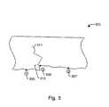
- FIG. 3is a simplified energy diagram 300 across a cleave front for the implanted substrate 10 having these defects.
- the diagram 300is merely an illustration and should not limit the scope of the claims herein.
- the diagramhas a vertical axis 301 which represents additional energy (E) and a horizontal axis 303 which represents a distance from side 1 to side 2 of the substrate, that is, the horizontal axis represents regions along the cleave front of the substrate.
- the cleave fronthas two regions 305 and 307 represented as region 1 and region 2 , respectively, which have cleave energies less than the average cleave energy (E cz ) 207 (possibly due to a higher concentration of defects or the like). Accordingly, it is highly likely that the cleave process begins at one or both of the above regions, since each region has a lower cleave energy than surrounding regions.
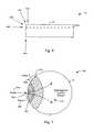
- FIG. 4is a simplified top-view diagram 400 of multiple cleave fronts 401 , 403 propagating through the implanted substrate.
- the cleave frontsoriginate at “weaker” regions in the cleave plane, which specifically includes regions 1 and 2 .
- the cleave frontsoriginate and propagate randomly as shown by the arrows.
- a limitation with the use of random propagation among multiple cleave frontsis the possibility of having different cleave fronts join along slightly different planes or the possibility of forming cracks, which is described in more detail below.
- FIG. 5is a simplified cross-sectional view 500 of a film cleaved from a wafer having multiple cleave fronts at, for example, regions 1 305 and 2 307 .
- This diagramis merely an illustration and should not limit the scope of the claims herein.
- the cleave from region 1 joined with the cleave from region 2 at region 3 309which is defined along slightly different planes, may initiate a secondary cleave or crack 311 along the film.
- the filmmay not be of sufficient quality for use in manufacture of substrates for integrated circuits or other applications.
- a substrate having crack 311generally cannot be used for processing.
- Brueldiscloses a technique for an “uncontrollable” cleaving action by way of initiating and maintaining a cleaving action by a global thermal source, which may produce undesirable results. These undesirable results include potential problems such as an imperfect joining of cleave fronts, an excessively rough surface finish on the surface of the cleaved material since the energy level for maintaining the cleave exceeds the amount required, and many others.
- the present inventionovercomes the formation of random cleave fronts by a controlled distribution or selective positioning of energy on the implanted substrate.
- FIG. 6is a simplified cross-sectional view of an implanted substrate 10 using selective positioning of cleave energy according to the present invention.
- the implanted waferundergoes a step of selective energy placement 601 or positioning or targeting which provides a controlled cleaving action of the material region 12 at the selected depth 603 .
- selected energy placement 607occurs near an edge or corner region of the selected depth 603 of substrate 10 .
- the impulse(or impulses) is provided using energy sources. Examples of sources include, among others, a chemical source, a mechanical source, an electrical source, and a thermal sink or source.
- the chemical sourcecan include a variety such as particles, fluids, gases, or liquids. These chemical sources can also include chemical reaction to increase stress in the material region.
- the chemical sourceis introduced as flood, time-varying, spatially varying, or continuous.
- a mechanical sourceis derived from rotational, translational, compressional, expansional, or ultrasonic energies.
- the mechanical sourcecan be introduced as flood, time-varying, spatially varying, or continuous.
- the electrical sourceis selected from an applied voltage or an applied electro-magnetic field, which is introduced as flood, time-varying, spatially varying, or continuous.
- the thermal source or sinkis selected from radiation, convection, or conduction.
- This thermal sourcecan be selected from, among others, a photon beam, a fluid jet, a liquid jet, a gas jet, an electro/magnetic field, an electron beam, a thermo-electric heating, a furnace, and the like.
- the thermal sinkcan be selected from a fluid jet, a liquid jet, a gas jet, a cryogenic fluid, a super-cooled liquid, a thermo-electric cooling means, an electro/magnetic field, and others. Similar to the previous embodiments, the thermal source is applied as flood, time-varying, spatially varying, or continuous. Still further, any of the above embodiments can be combined or even separated, depending upon the application. Of course, the type of source used depends upon the application.
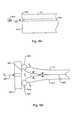
- the energy sourcecan be a fluid jet that is pressurized (e.g., compressional) according to an embodiment of the present invention.
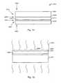
- FIG. 6Ashows a simplified cross-sectional view diagram of a fluid jet from a fluid nozzle 608 used to perform the controlled cleaving process according to an embodiment of the present invention.
- the fluid jet 607(or liquid jet or gas jet) impinges on an edge region of substrate 10 to initiate the controlled cleaving process.
- the fluid jet from a compressed or pressurized fluid sourceis directed to a region at the selected depth 603 to cleave a thickness of material region 12 from substrate 10 using force, e.g., mechanical, chemical, thermal.
- the fluid jetseparates substrate 10 into two regions, including region 609 and region 611 that separate from each other at selected depth 603 .
- the fluid jetcan also be adjusted to initiate and maintain the controlled cleaving process to separate material 12 from substrate 10 .
- the fluid jetcan be adjusted in direction, location, and magnitude to achieve the desired controlled cleaving process.
- the fluid jetcan be a liquid jet or a gas jet or a combination of liquid and gas.
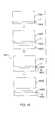
- the energy sourcecan be a compressional source such as, for example, compressed fluid that is static.
- FIG. 6Bshows a simplified cross-sectional view diagram of a compressed fluid source 607 according to an embodiment of the present invention.
- the compressed fluid source 607e.g., pressurized liquid, pressurized gas
- a sealed chamber 621which surrounds a periphery or edge of the substrate 10 .
- the chamberis enclosed by device 623 , which is sealed by, for example, o-rings 625 or the like, and which surrounds the outer edge of the substrate.
- the chamberhas a pressure maintained at P c that is applied to the edge region of substrate 10 to initiate the controlled cleaving process at the selected depth of implanted material.
- the outer surface or face of the substrateis maintained at pressure P A which can be ambient pressure e.g., 1 atmosphere or less.
- P Acan be ambient pressure e.g., 1 atmosphere or less.
- a pressure differentialexists between the pressure in the chamber, which is higher, and the ambient pressure. The pressure difference applies force to the implanted region at the selected depth 603 .
- the implanted region at the selected depthis structurally weaker than surrounding regions, including any bonded regions. Force is applied via the pressure differential until the controlled cleaving process is initiated.
- the controlled cleaving processseparates the thickness of material 609 from substrate material 611 to split the thickness of material from the substrate material at the selected depth.
- pressure P cforces material region 12 to separate by a “prying action” from substrate material 611 .
- the pressure in the chambercan also be adjusted to initiate and maintain the controlled cleaving process to separate material 12 from substrate 10 .
- the pressurecan be adjusted in magnitude to achieve the desired controlled cleaving process.
- the fluid pressurecan be derived from a liquid or a gas or a combination of liquid and gas.
- the present inventionprovides a controlled-propagating cleave.
- the controlled-propagating cleaveuses multiple successive impulses to initiate and perhaps propagate a cleaving process 700 , as illustrated by FIG. 7.
- the impulseis directed at an edge of the substrate, which propagates a cleave front toward the center of the substrate to remove the material layer from the substrate.
- a sourceapplies multiple pulses (i.e., pulse 1 , 2 , and 3 ) successively to the substrate.
- Pulse 1 701is directed to an edge 703 of the substrate to initiate the cleave action.
- Pulse 2 705is also directed at the edge 707 on one side of pulse 1 to expand the cleave front.
- Pulse 3 709is directed to an opposite edge 711 of pulse 1 along the expanding cleave front to further remove the material layer from the substrate. The combination of these impulses or pulses provides a controlled cleaving action 713 of the material layer from the substrate.
- FIG. 8is a simplified illustration of selected energies 800 from the pulses in the preceding embodiment for the controlled-propagating cleave.
- the pulse 1has an energy level which exceeds average cleaving energy (E), which is the necessary energy for initiating the cleaving action.
- Pulses 2 and 3are made using lower energy levels along the cleave front to maintain or sustain the cleaving action.
- the pulseis a laser pulse where an impinging beam heats a selected region of the substrate through a pulse and a thermal pulse gradient causes supplemental stresses which together exceed cleave formation or propagation energies, which create a single cleave front.
- the impinging beamheats and causes a thermal pulse gradient simultaneously, which exceed cleave energy formation or propagation energies. More preferably, the impinging beam cools and causes a thermal pulse gradient simultaneously, which exceed cleave energy formation or propagation energies.
- a built-in energy state of the substrate or stresscan be globally raised toward the energy level necessary to initiate the cleaving action, but not enough to initiate the cleaving action before directing the multiple successive impulses to the substrate according to the present invention.
- the global energy state of the substratecan be raised or lowered using a variety of sources such as chemical, mechanical, thermal (sink or source), or electrical, alone or in combination.
- the chemical sourcecan include a variety such as particles, fluids, gases, or liquids. These sources can also include chemical reaction to increase stress in the material region.
- the chemical sourceis introduced as flood, time-varying, spatially varying, or continuous.
- a mechanical sourceis derived from rotational, translational, compressional, expansional, or ultrasonic energies.
- the mechanical sourcecan be introduced as flood, time-varying, spatially varying, or continuous.
- the electrical sourceis selected from an applied voltage or an applied electro-magnetic field, which is introduced as flood, time-varying, spatially varying, or continuous.
- the thermal source or sinkis selected from radiation, convection, or conduction. This thermal source can be selected from, among others, a photon beam, a fluid jet, a liquid jet, a gas jet, an electro/magnetic field, an electron beam, a thermo-electric heating, and a furnace.
- the thermal sinkcan be selected from a fluid jet, a liquid jet, a gas jet, a cryogenic fluid, a super-cooled liquid, a thermo-electric cooling means, an electro/magnetic field, and others. Similar to the previous embodiments, the thermal source is applied as flood, time-varying, spatially varying, or continuous. Still further, any of the above embodiments can be combined or even separated, depending upon the application. Of course, the type of source used also depends upon the application. As noted, the global source increases a level of energy or stress in the material region without initiating a cleaving action in the material region before providing energy to initiate the controlled cleaving action.
- an energy sourceelevates an energy level of the substrate cleave plane above its cleave front propagation energy but is insufficient to cause self-initiation of a cleave front.
- a thermal energy source or sink in the form of heat or lack of heate.g., cooling source
- the energy sourcecan be electrical, chemical, or mechanical.
- a directed energy sourceprovides an application of energy to a selected region of the substrate material to initiate a cleave front which self-propagates through the implanted region of the substrate until the thin film of material is removed.
- a variety of techniquescan be used to initiate the cleave action. These techniques are described by way of the Figs. below.
- FIG. 9is a simplified illustration of an energy state 900 for a controlled cleaving action using a single controlled source according to an aspect of the present invention.
- the energy level or state of the substrateis raised using a global energy source above the cleave front propagation energy state, but is lower than the energy state necessary to initiate the cleave front.
- an energy sourcesuch as a laser directs a beam in the form of a pulse at an edge of the substrate to initiate the cleaving action.
- the energy sourcecan be a cooling fluid (e.g., liquid, gas) that directs a cooling medium in the form of a pulse at an edge of the substrate to initiate the cleaving action.
- the global energy sourcemaintains the cleaving action which generally requires a lower energy level than the initiation energy.
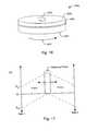
- FIG. 10is a simplified illustration of an implanted substrate 1000 undergoing rotational forces 1001 , 1003 .
- the substrateincludes a top surface 1005 , a bottom surface 1007 , and an implanted region 1009 at a selected depth.
- An energy sourceincreases a global energy level of the substrate using a light beam or heat source to a level above the cleave front propagation energy state, but lower than the energy state necessary to initiate the cleave front.
- the substrateundergoes a rotational force turning clockwise 1001 on top surface and a rotational force turning counter-clockwise 1003 on the bottom surface which creates stress at the implanted region 1009 to initiate a cleave front.
- the top surfaceundergoes a counter-clockwise rotational force and the bottom surface undergoes a clockwise rotational force.
- the direction of the forcegenerally does not matter in this embodiment.
- FIG. 11is a simplified diagram of an energy state 1100 for the controlled cleaving action using the rotational force according to the present invention.
- This diagramis merely an illustration, and should not limit the scope of the claims herein.
- the energy level or state of the substrateis raised using a global energy source (e.g., thermal, beam) above the cleave front propagation energy state, but is lower than the energy state necessary to initiate the cleave front.
- a mechanical energy meanssuch as rotational force applied to the implanted region initiates the cleave front.
- rotational force applied to the implanted region of the substratescreates zero stress at the center of the substrate and greatest at the periphery, essentially being proportional to the radius.
- the central initiating pulsecauses a radially expanding cleave front to cleave the substrate.
- the removed material regionprovides a thin film of silicon material for processing.
- the silicon materialpossesses limited surface roughness and desired planarity characteristics for use in a silicon-on-insulator substrate.
- the surface roughness of the detached filmhas features that are less than about 60 nm, or less than about 40 nm, or less than about 20 nm. Accordingly, the present invention provides thin silicon films which can be smoother and more uniform than pre-existing techniques.
- the present inventionis practiced at temperatures that are lower than those used by pre-existing techniques.
- the present inventiondoes not require increasing the entire substrate temperature to initiate and sustain the cleaving action as pre-existing techniques.
- substrate temperaturedoes not exceed about 400° C. during the cleaving process.
- substrate temperaturedoes not exceed about 350° C. during the cleaving process.
- substrate temperatureis kept substantially below implanting temperatures via a thermal sink, e.g., cooling fluid, cryogenic fluid.
- the present inventionreduces a possibility of unnecessary damage from an excessive release of energy from random cleave fronts, which generally improves surface quality of a detached film(s) and/or the substrate(s). Accordingly, the present invention provides resulting films on substrates at higher overall yields and quality.
- the above embodimentsare described in terms of cleaving a thin film of material from a substrate.
- the substratecan be disposed on a workpiece such as a stiffener or the like before the controlled cleaving process.
- the workpiecejoins to a top surface or implanted surface of the substrate to provide structural support to the thin film of material during controlled cleaving processes.
- the workpiececan be joined to the substrate using a variety of bonding or joining techniques, e.g., electro-statics, adhesives, interatomic. Some of these bonding techniques are described herein.
- the workpiececan be made of a dielectric material (e.g., quartz, glass, sapphire, silicon nitride, silicon dioxide), a conductive material (silicon, silicon carbide, polysilicon, group III/V materials, metal), and plastics (e.g., polyimide-based materials).
- a dielectric materiale.g., quartz, glass, sapphire, silicon nitride, silicon dioxide
- a conductive materialsilicon, silicon carbide, polysilicon, group III/V materials, metal
- plasticse.g., polyimide-based materials
- the substrate having the film to be detachedcan be temporarily disposed on a transfer substrate such as a stiffener or the like before the controlled cleaving process.
- the transfer substratejoins to a top surface or implanted surface of the substrate having the film to provide structural support to the thin film of material during controlled cleaving processes.
- the transfer substratecan be temporarily joined to the substrate having the film using a variety of bonding or joining techniques, e.g., electro-statics, adhesives, interatomic. Some of these bonding techniques are described herein.
- the transfer substratecan be made of a dielectric material (e.g., quartz, glass, sapphire, silicon nitride, silicon dioxide), a conductive material (silicon, silicon carbide, polysilicon, group III/V materials, metal), and plastics (e.g., polyimide-based materials).
- a dielectric materiale.g., quartz, glass, sapphire, silicon nitride, silicon dioxide
- a conductive materialsilicon, silicon carbide, polysilicon, group III/V materials, metal
- plasticse.g., polyimide-based materials
- a process for fabricating a silicon-on-insulator substrate according to the present inventionmay be briefly outlined as follows:
- the above sequence of stepsprovides a step of initiating a controlled cleaving action using an energy applied to a selected region(s) of a multi-layered substrate structure to form a cleave front(s) according to the present invention.
- This initiation stepbegins a cleaving process in a controlled manner by limiting the amount of energy applied to the substrate. Further propagation of the cleaving action can occur by providing additional energy to selected regions of the substrate to sustain the cleaving action, or using the energy from the initiation step to provide for further propagation of the cleaving action.
- This sequence of stepsis merely an example and should not limit the scope of the claims defined herein. Further details with regard to the above sequence of steps are described in below in references to the Figs.
- FIGS. 12 - 18are simplified cross-sectional view diagrams of substrates undergoing a fabrication process for a silicon-on-insulator wafer according to the present invention.
- the processbegins by providing a semiconductor substrate similar to the silicon wafer 2100 , as shown by FIG. 12.
- Substrate or donorincludes a material region 2101 to be removed, which is a thin relatively uniform film derived from the substrate material.
- the silicon waferincludes a top surface 2103 , a bottom surface 2105 , and a thickness 2107 .
- Material regionalso includes a thickness (z 0 ), within the thickness 2107 of the silicon wafer.
- a dielectric layer 2102(e.g., silicon nitride, silicon oxide, silicon oxynitride) overlies the top surface of the substrate.
- the present processprovides a novel technique for removing the material region 2101 using the following sequence of steps for the fabrication of a silicon-on-insulator wafer.
- Selected energetic particles 2109implant through the top surface of the silicon wafer to a selected depth, which defines the thickness of the material region, termed the thin film of material. As shown, the particles have a desired concentration 2111 at the selected depth (z 0 ).
- a variety of techniquescan be used to implant the energetic particles into the silicon wafer. These techniques include ion implantation using, for example, beam line ion implantation equipment manufactured from companies such as Applied Materials, Eaton Corporation, Varian, and others. Alternatively, implantation occurs using a plasma immersion ion implantation (“PIII”) technique. Furthermore, implantation can occur using ion shower. Of course, techniques used depend upon the application.
- smaller mass particlesare generally selected to reduce a possibility of damage to the material region. That is, smaller mass particles easily travel through the substrate material to the selected depth without substantially damaging the material region that the particles traversed through.
- the smaller mass particlesor energetic particles
- the particlescan be almost any charged (e.g., positive or negative) and/or neutral atoms or molecules, or electrons, or the like.
- the particlescan be neutral and/or charged particles including ions of hydrogen and its isotopes, rare gas ions such as helium and its isotopes, and neon.
- the particlescan also be derived from compounds such as gases, e.g., hydrogen gas, water vapor, methane, and other hydrogen compounds, and other light atomic mass particles.
- gasese.g., hydrogen gas, water vapor, methane, and other hydrogen compounds
- the particlescan be any combination of the above particles, and/or ions and/or molecular species and/or atomic species.
- the processuses a step of joining the implanted silicon wafer to a workpiece or target wafer, as illustrated in FIG. 13.
- the workpiecemay also be a variety of other types of substrates such as those made of a dielectric material (e.g., quartz, glass, silicon nitride, silicon dioxide), a conductive material (silicon, polysilicon, group III/V materials, metal), and plastics (e.g., polyimide-based materials).
- a dielectric materiale.g., quartz, glass, silicon nitride, silicon dioxide
- a conductive materialsilicon, polysilicon, group III/V materials, metal
- plasticse.g., polyimide-based materials
- the silicon wafersare joined or fused together using a low temperature thermal step.
- the low temperature thermal processgenerally ensures that the implanted particles do not place excessive stress on the material region, which can produce an uncontrolled cleave action.
- the low temperature bonding processoccurs by a self-bonding process.
- one waferis stripped to remove oxidation therefrom (or one wafer is not oxidized).
- a cleaning solutiontreats the surface of the wafer to form O—H bonds on the wafer surface.
- An example of a solution used to clean the waferis a mixture of H 2 O 2 —H 2 SO 4 .
- a dryerdries the wafer surfaces to remove any residual liquids or particles from the wafer surfaces.
- Self-bondingoccurs by placing a face of the cleaned wafer against the face of an oxidized wafer.
- a self-bonding processoccurs by activating one of the wafer surfaces to be bonded by plasma cleaning.
- plasma cleaningactivates the wafer surface using a plasma derived from gases such as argon, ammonia, neon, water vapor, and oxygen.
- the activated wafer surface 2203is placed against a face of the other wafer, which has a coat of oxidation 2205 thereon.
- the wafersare in a sandwiched structure having exposed wafer faces. A selected amount of pressure is placed on each exposed face of the wafers to self-bond one wafer to the other.
- an adhesive disposed on the wafer surfacesis used to bond one wafer onto the other.
- the adhesiveincludes an epoxy, polyimide-type materials, and the like.
- Spin-on-glass layerscan be used to bond one wafer surface onto the face of another.
- These spin-on-glass (“SOG”) materialsinclude, among others, siloxanes or silicates, which are often mixed with alcohol-based solvents or the like. SOG can be a desirable material because of the low temperatures (e.g., 150 to 250° C.) often needed to cure the SOG after it is applied to surfaces of the wafers.
- a variety of other low temperature techniquescan be used to join the donor wafer to the target wafer.
- an electro-static bonding techniquecan be used to join the two wafers together.
- one or both wafer surface(s)is charged to attract to the other wafer surface.
- the donor wafercan be fused to the target wafer using a variety of commonly known techniques. Of course, the technique used depends upon the application.
- the methodincludes a controlled cleaving action to remove the substrate material to provide a thin film of substrate material 2101 overlying an insulator 2305 the target silicon wafer 2201 .
- the controlled-cleavingoccurs by way of selective energy placement or positioning or targeting 2301 , 2303 of energy sources onto the donor and/or target wafers.
- an energy impluse(s)can be used to initiate the cleaving action.
- the impulseis provided using an energy source which include, among others, a mechanical source, a chemical source, a thermal sink or source, and an electrical source.
- the controlled cleaving actionis initiated by way of any of the previously noted techniques and others and is illustrated by way of FIG. 14.
- a process for initiating the controlled cleaving actionuses a step of providing energy 2301 , 2303 to a selected region of the substrate to initiate a controlled cleaving action at the selected depth (z 0 ) in the substrate, whereupon the cleaving action is made using a propagating cleave front to free a portion of the substrate material to be removed from the substrate.
- the methoduses a single impulse to begin the cleaving action, as previously noted.
- the methoduses an initiation impulse, which is followed by another impulse or successive impulses to selected regions of the substrate.
- the methodprovides an impulse to initiate a cleaving action which is sustained by a scanned energy along the substrate.
- energycan be scanned across selected regions of the substrate to initiate and/or sustain the controlled cleaving action.
- an energy or stress of the substrate materialis increased toward an energy level necessary to initiate the cleaving action, but not enough to initiate the cleaving action before directing an impulse or multiple successive impulses to the substrate according to the present invention.
- the global energy state of the substratecan be raised or lowered using a variety of sources such as chemical, mechanical, thermal (sink or source), or electrical, alone or in combination.
- the chemical sourcecan include particles, fluids, gases, or liquids. These sources can also include chemical reaction to increase stress in the material region.
- the chemical sourceis introduced as flood, time-varying, spatially varying, or continuous.
- a mechanical sourceis derived from rotational, translational, compressional, expansional, or ultrasonic energies.
- the mechanical sourcecan be introduced as flood, time-varying, spatially varying, or continuous.
- the electrical sourceis selected from an applied voltage or an applied electro-magnetic field, which is introduced as flood, time-varying, spatially varying, or continuous.
- the thermal source or sinkis selected from radiation, convection, or conduction. This thermal source can be selected from, among others, a photon beam, a fluid jet, a liquid jet, a gas jet, an electro/magnetic field, an electron beam, a thermo-electric heating, and a furnace.
- the thermal sinkcan be selected from a fluid jet, a liquid jet, a gas jet, a cryogenic fluid, a super-cooled liquid, a thermo-electric cooling means, an electro/magnetic field, and others. Similar to the previous embodiments, the thermal source is applied as flood, time-varying, spatially varying, or continuous. Still further, any of the above embodiments can be combined or even separated, depending upon the application. Of course, the type of source used depends upon the application. As noted, the global source increases a level of energy or stress in the material region without initiating a cleaving action in the material region before providing energy to initiate the controlled cleaving action.
- the methodmaintains a temperature which is below a temperature of introducing the particles into the substrate.
- the substrate temperatureis maintained between ⁇ 200 and 450° C. during the step of introducing energy to initiate propagation of the cleaving action.
- Substrate temperaturecan also be maintained at a temperature below 400° C. or below 350° C.
- the methoduses a thermal sink to initiate and maintain the cleaving action, which occurs at conditions significantly below room temperature.
- the mechanical and/or thermal sourcecan be a fluid jet that is pressurized (e.g., compressional) according to an embodiment of the present invention.
- the fluid jet(or liquid jet or gas jet) impinges on an edge region of substrate 2300 to initiate the controlled cleaving process.
- the fluid jet from a compressed or pressurized fluid sourceis directed to a region at the selected depth 2111 to cleave a thickness of material region 2101 from substrate 2100 .
- the fluid jetseparates region 2101 from substrate 2100 that separate from each other at selected depth 2111 .
- the fluid jetcan be adjusted to initiate and maintain the controlled cleaving process to separate material 2101 from substrate 2100 .
- the fluid jetcan be adjusted in direction, location, and magnitude to achieve the desired controlled cleaving process.
- a final bonding stepoccurs between the target wafer and thin film of material region according to some embodiments, as illustrated by FIG. 15.
- one silicon waferhas an overlying layer of silicon dioxide, which is thermally grown overlying the face before cleaning the thin film of material.
- the silicon dioxidecan also be formed using a variety of other techniques, e.g., chemical vapor deposition. The silicon dioxide between the wafer surfaces fuses together thermally in this process.
- the oxidized silicon surface from either the target wafer or the thin film of material region (from the donor wafer)are further pressed together and are subjected to an oxidizing ambient 2401 .
- the oxidizing ambientcan be in a diffusion furnace for steam oxidation, hydrogen oxidation, or the like.
- a combination of the pressure and the oxidizing ambientfuses the two silicon wafers together at the oxide surface or interface 2305 .
- These embodimentsoften require high temperatures (e.g., 700° C.).
- the two silicon surfacesare further pressed together and subjected to an applied voltage between the two wafers.
- the applied voltageraises temperature of the wafers to induce a bonding between the wafers.
- This techniquelimits the amount of crystal defects introduced into the silicon wafers during the bonding process, since substantially no mechanical force is needed to initiate the bonding action between the wafers.
- the technique useddepends upon the application.
- silicon-on-insulatorAfter bonding the wafers, silicon-on-insulator has a target substrate with an overlying film of silicon material and a sandwiched oxide layer between the target substrate and the silicon film, as also illustrated in FIG. 15.
- the detached surface of the film of silicon materialis often rough 2404 and needs finishing. Finishing occurs using a combination of grinding and/or polishing techniques.
- the detached surfaceundergoes a step of grinding using, for examples, techniques such as rotating an abrasive material overlying the detached surface to remove any imperfections or surface roughness therefrom.
- a machinesuch as a “back grinder” made by a company called Disco may provide this technique.
- CMPchemical mechanical polishing or planarization
- the abrasiveis often a borosilicate glass, titanium dioxide, titanium nitride, aluminum oxide, aluminum trioxide, iron nitrate, cerium oxide, silicon dioxide (colloidal silica), silicon nitride, silicon carbide, graphite, diamond, and any mixtures thereof.
- This abrasiveis mixed in a solution of deionized water and oxidizer or the like.
- the solutionis acidic.
- This acid solutiongenerally interacts with the silicon material from the wafer during the polishing process.
- the polishing processpreferably uses a polyurethane polishing pad.
- An example of this polishing padis one made by Rodel and sold under the tradename of IC-1000.
- the polishing padis rotated at a selected speed.
- a carrier headwhich picks up the target wafer having the film applies a selected amount of pressure on the backside of the target wafer such that a selected force is applied to the film.
- the polishing processremoves about a selected amount of film material, which provides a relatively smooth film surface 2601 for subsequent processing, as illustrated by FIG. 17.
- a thin film of oxide 2406overlies the film of material overlying the target wafer, as illustrated in FIG. 15.
- the oxide layerforms during the thermal annealing step, which is described above for permanently bonding the film of material to the target wafer.
- the finishing processis selectively adjusted to first remove oxide and the film is subsequently polished to complete the process.
- the sequence of stepsdepends upon the particular application.
- the silicon-on-insulator substrateundergoes a series of process steps for formation of integrated circuits thereon. These processing steps are described in S. Wolf, Silicon Processing for the VLSI Era (Volume 2), Lattice Press (1990), which is hereby incorporated by reference for all purposes.
- a portion of a completed wafer 2700 including integrated circuit devicesis illustrated by FIG. 18. As shown, the portion of the wafer 2700 includes active devices regions 2701 and isolation regions 2703 .
- the active devicesare field effect transistors each having a source/drain region 2705 and a gate electrode 2707 .
- a dielectric isolation layer 2709is defined overlying the active devices to isolate the active devices from any overlying layers.
- the substratecan be almost any monocrystalline, polycrystalline, or even amorphous type substrate.
- the substratecan be made of III/V materials such as gallium arsenide, gallium nitride (GaN), and others.
- the multi-layered substratecan also be used according to the present invention.
- the multi-layered substrateincludes a silicon-on-insulator substrate, a variety of sandwiched layers on a semiconductor substrate, and numerous other types of substrates. Additionally, the embodiments above were generally in terms of providing a pulse of energy to initiate a controlled cleaving action.
- the pulsecan be replaced by energy that is scanned across a selected region of the substrate to initiate the controlled cleaving action. Energy can also be scanned across selected regions of the substrate to sustain or maintain the controlled cleaving action.
- a donor substrate 1902is shown with an overlayer 1904 disposed upon a surface of the donor substrate.
- the overlayermay be, but is not limited to, semiconductor material, a dielectric layer, a layer of metal, a ceramic material, a polymer, or some combination of the foregoing.
- the interfacial bonding strength at the interfaceis represented by the quantity E 1 .
- the donor substrate/overlayer assemblyis then bonded to a receptor (handle) substrate 1922 .
- a receptor (handle) substrate 1922As can be seen in the Fig. an interface 12 is formed between a surface of the receptor substrate and a surface of the overlayer 1904 .
- the interfacial bonding energy at interface I 2is represented by the quantity E 2 , where E 2 >E 1 .
- the foregoing disclosed controlled cleaving processis applied to the assembly 1901 .
- a cleaving strength represented by the quantity E p(referred to above as the cleave front propagation energy), where E 2 >E p >E 1 , is applied.
- E pthe cleaving strength
- E 2 >E p >E 1the bonding strength
- the CCP processdoes not separate the overlayer from the handle substrate.
- the bonding strength (E 2 )can be increased; for example, by interfacial diffusion, alloying, compound formation, and so on.
- the overlayer 1904is a surface slice of the donor substrate 1902 (e.g., a silicon wafer having a layer of oxidized silicon formed thereon).
- interface I 1is created by the implantation of hydrogen into the donor wafer.
- the handle wafer 1922is layer of oxidized silicon formed atop the donor wafer, the interface I 2 being the interface between the silicon of the donor substrate and the oxidized silicon layer.
- Application of the CCP processcreates an SOI (silicon-on-insulator) wafer by separation at the interface I 1 .
- the donor substrate 1902is a SiO 2 -covered substrate.
- the overlayer 1904is a Cu thin film deposited on the SiO 2 layer of the donor substrate.
- a handle substrate 1922is provided with a surface layer of TiN.
- the overlayer 1904is attached to the TiN layer of the handle substrate.
- Cuadheres very well to TiN. However, Cu does not adhere well to SiO 2 .
- a subsequent CCP cleavecauses the overlayer to separate from the SiO 2 of the donor substrate, thus effecting a transfer of the overlayer to the handle substrate.
- the donor substrate 1902is coated with a porous oxide substrate (e.g., a CVD or implanted/plasma treated porous oxide).
- the overlayer 1904is an ion-cut piece of Si crystal film. The overlayer is transferred to the donor substrate with the Genesis process (bond and CCP). The interface I 1 is weak, due to the porous nature of the oxide.
- the Si layeris subjected to normal IC fabrication steps to make integrated circuits. After completion, the surface is coated with SiO 2 . Now the whole assembly is considered to be the donor substrate assembly.
- the donor assemblyis bonded to an oxidized Si wafer which acts as the handle wafer 1922 .
- the bond strength E 2can be increased by elevating the temperature in a thermal treatment step. Since there is no implanted hydrogen, there are no concerns with cracking during the thermal treatment. A CCP step can be carried out to cause delamination at the weak interface I 1 , thus effecting a transfer of the entire IC layer to the handle wafer.
- Step 1Create an overlayer 1904 atop the surface of a donor substrate 1902 , where the interface I 1 between the overlayer and donor substrate has a bonding strength E 1 .
- the bonding strength of interface I 1can be controlled by the choice of the overlayer material and the donor substrate material.
- Other means for controlling the bonding strengthinclude, but are not limited to the use of an interfacial adhesion weakening layer (e.g., a surfactant), implantation of particles at the depth of interface I 1 to weaken the atomic bonds, plasma treatment of the donor substrate surface to weaken surface bonding mechanisms, or combinations of the foregoing.
- an interfacial adhesion weakening layere.g., a surfactant
- implantation of particles at the depth of interface I 1 to weaken the atomic bondsimplantation of particles at the depth of interface I 1 to weaken the atomic bonds
- plasma treatment of the donor substrate surface to weaken surface bonding mechanismsor combinations of the foregoing.
- Step 2Intimately contacting at an interface I 2 the planar face of the donor substrate/overlayer assembly with a handle substrate 1922 .
- the bonding strength E 2 at interface I 2is controlled by factors including, but not limited to, the choice of overlayer and donor substrate materials, the addition of an interfacial adhesion strengthening layer (e.g., an adhesive), plasma treatment of the handle substrate to activate bonding mechanisms, or combinations of the foregoing.
- an interfacial adhesion strengthening layere.g., an adhesive
- Step 3Performing a controlled cleavage process (CCP) with a cleaving strength E p , where E 2 >E p >E 1 .
- CCPcontrolled cleavage process
- Step 4(optional).
- the bonding strength E 2 of interface I 2can be increased to full strength by further process treatments, such as interfacial diffusion, alloying, or compound formation, and so on.
- the CCP stepcan be performed at room temperature, or at temperatures above or below the preparation temperature of the overlayer 1904 .
- both the donor substrate and the handle substratehave sufficient mechanical stiffness to withstand the CCP process.
- the overlayercan have patterned structures.
Landscapes
- Engineering & Computer Science (AREA)
- Physics & Mathematics (AREA)
- Microelectronics & Electronic Packaging (AREA)
- Manufacturing & Machinery (AREA)
- Power Engineering (AREA)
- Condensed Matter Physics & Semiconductors (AREA)
- General Physics & Mathematics (AREA)
- Computer Hardware Design (AREA)
- High Energy & Nuclear Physics (AREA)
- Toxicology (AREA)
- Health & Medical Sciences (AREA)
- Chemical & Material Sciences (AREA)
- Materials Engineering (AREA)
- Plasma & Fusion (AREA)
- Spectroscopy & Molecular Physics (AREA)
- Processing Of Stones Or Stones Resemblance Materials (AREA)
- Element Separation (AREA)
- Recrystallisation Techniques (AREA)
- Dicing (AREA)
- Crystals, And After-Treatments Of Crystals (AREA)
- Re-Forming, After-Treatment, Cutting And Transporting Of Glass Products (AREA)
Abstract
Description
- This application claims priority to U.S. patent application Ser. No. 09/301,082, filed Apr. 28, 1999, which claim priority to U.S. Provisional Application No. 60/083,453 filed Apr. 29, 1998 and to U.S. application Ser. No. 09/026,027 filed Feb. 19, 1998, now U.S. Pat. No. 5,994,207, which claims priority to U.S. Provisional Application No. 60/046,276 filed May 12, 1997, all of which are incorporated by reference for all purposes.[0001]
- The present invention relates to the manufacture of substrates. More particularly, the invention provides a technique including a method and device for cleaving a substrate in the fabrication of a silicon-on-insulator substrate for semiconductor integrated circuits using a pressurized fluid, for example. But it will be recognized that the invention has a wider range of applicability; it can also be applied to other substrates for multi-layered integrated circuit devices, three-dimensional packaging of integrated semiconductor devices, photonic devices, piezoelectronic devices, microelectromechanical systems (“MEMS”), sensors, actuators, solar cells, flat panel displays (e.g., LCD, AMLCD), biological and biomedical devices, and the like.[0002]
- Craftsmen or more properly crafts-people have been building useful articles, tools, or devices using less useful materials for numerous years. In some cases, articles are assembled by way of smaller elements or building blocks. Alternatively, less useful articles are separated into smaller pieces to improve their utility. A common example of these articles to be separated include substrate structures such as a glass plate, a diamond, a semiconductor substrate, and others.[0003]
- These substrate structures are often cleaved or separated using a variety of techniques. In some cases, the substrates can be cleaved using a saw operation. The saw operation generally relies upon a rotating blade or tool, which cuts through the substrate material to separate the substrate material into two pieces. This technique, however, is often extremely “rough” and cannot generally be used for providing precision separations in the substrate for the manufacture of fine tools and assemblies. Additionally, the saw operation often has difficulty separating or cutting extremely hard and/or brittle materials such as diamond or glass.[0004]
- Accordingly, techniques have been developed to separate these hard and/or brittle materials using cleaving approaches. In diamond cutting, for example, an intense directional thermal/mechanical impulse is directed preferentially along a crystallographic plane of a diamond material. This thermal/mechanical impulse generally causes a cleave front to propagate along major crystallographic planes, where cleaving occurs when an energy level from the thermal/mechanical impulse exceeds the fracture energy level along the chosen crystallographic plane.[0005]
- In glass cutting, a scribe line using a tool is often impressed in a preferred direction on the glass material, which is generally amorphous in character. The scribe line causes a higher stress area surrounding the amorphous glass material. Mechanical force is placed on each side of the scribe line, which increases stress along the scribe line until the glass material fractures, preferably along the scribe line. This fracture completes the cleaving process of the glass, which can be used in a variety of applications including households.[0006]
- Although the techniques described above are satisfactory, for the most part, as applied to cutting diamonds or household glass, they have severe limitations in the fabrication of small complex structures or precision workpieces. For instance, the above techniques are often “rough” and cannot be used with great precision in fabrication of small and delicate machine tools, electronic devices, or the like. Additionally, the above techniques may be useful for separating one large plane of glass from another, but are often ineffective for splitting off, shaving, or stripping a thin film of material from a larger substrate. Furthermore, the above techniques may often cause more than one cleave front, which join along slightly different planes, which is highly undesirable for precision cutting applications.[0007]
- From the above, it is seen that a technique for separating a thin film of material from a substrate which is cost effective and efficient is often desirable.[0008]
- According to the present invention, an improved technique for removing a thin film of material from a substrate using a controlled cleaving action is provided. This technique allows an initiation of a cleaving process on a substrate using a single or multiple cleave region(s) through the use of controlled energy (e.g., spatial distribution) and selected conditions to allow an initiation of a cleave front(s) and to allow it to propagate through the substrate to remove a thin film of material from the substrate.[0009]
- In a specific embodiment, the present invention provides a process for forming a film of material from a donor substrate using a controlled cleaving process. The process includes forming a weakened region at a selected depth underneath the surface to define a thickness of donor substrate material (e.g., thin film of detachable material) above the selected depth. To cleave the donor substrate material, the method provides energy to a selected region of the donor substrate to initiate a controlled cleaving action in the donor substrate, whereupon the cleaving action is made using a propagating cleave front(s) to free the donor material from a remaining portion of the donor substrate.[0010]
- In most of the embodiments, a cleave is initiated by subjecting the material with sufficient energy to fracture the material in one region, causing a cleave front, without uncontrolled shattering or cracking. The cleave front formation energy (E[0011]c) must often be made lower than the bulk material fracture energy (Emat) at each region to avoid shattering or cracking the material. The directional energy impulse vector in diamond cutting or the scribe line in glass cutting are, for example, the means in which the cleave energy is reduced to allow the controlled creation and propagation of a cleave front. The cleave front is in itself a higher stress region and once created, its propagation requires a lower energy to further cleave the material from this initial region of fracture. The energy required to propagate the cleave front is called the cleave front propagation energy (Ep). The relationship can be expressed as:
- Ec=Ep+[cleave front stress energy]
- A controlled cleaving process is realized by reducing E[0012]palong a favored direction(s) above all others and limiting the available energy to be below the Epof other undesired directions. In any cleave process, a better cleave surface finish occurs when the cleave process occurs through only one expanding cleave front, although multiple cleave fronts do work.
- Numerous benefits are achieved over pre-existing techniques using the present invention. In particular, the present invention uses controlled energy and selected conditions to preferentially cleave a thin film of material from a donor substrate which includes multi-material sandwiched films. This cleaving process selectively removes the thin film of material from the substrate while preventing a possibility of damage to the film or a remaining portion of the substrate. Accordingly, the remaining substrate portion can be re-used repeatedly for other applications.[0013]
- Additionally, the present invention uses a relatively low temperature during the controlled cleaving process of the thin film to reduce temperature excursions of the separated film, donor substrate, or multi-material films according to other embodiments. In most cases, the controlled cleaving process can occur at, for example, room temperature, as well as others. This lower temperature approach allows for more material and process latitude such as, for example, cleaving and bonding of materials having substantially different thermal expansion coefficients. In other embodiments, the present invention limits energy or stress in the substrate to a value below a cleave initiation energy, which generally removes a possibility of creating random cleave initiation sites or fronts. This reduces cleave damage (e.g., pits, crystalline defects, breakage, cracks, steps, voids, excessive roughness) often caused in pre-existing techniques. Moreover, the present invention reduces damage caused by higher than necessary stress or pressure effects and nucleation sites caused by the energetic particles as compared to pre-existing techniques.[0014]
- [0015]
Exhibit 1, which is hereby incorporated by reference, discloses additional embodiments of the present invention. - The present invention achieves these benefits and others in the context of known process technology. However, a further understanding of the nature and advantages of the present invention may be realized by reference to the latter portions of the specification and attached drawings.[0016]
- FIGS.[0017]1-11 are simplified diagrams illustrating a controlled cleaving technique according to an embodiment of the present invention;
- FIGS.[0018]12-18 are simplified cross-sectional view diagrams illustrating a method of forming a silicon-on-insulator substrate according to the present invention; and
- FIG. 19 is shows a simplified sequence illustrating a method for a wafer transfer technique in accordance with another embodiment of the invention[0019]
- The present invention provides a technique for removing a thin film of material from a substrate while preventing a possibility of damage to the thin material film and/or a remaining portion of the substrate. The thin film of material is attached to or can be attached to a target substrate to form, for example, a silicon-on-insulator wafer. The thin film of material can also be used for a variety of other applications. The invention will be better understood by reference to the Figs. and the descriptions below.[0020]
- 1. Controlled Cleaving Techniques[0021]
- FIG. 1 is a simplified cross-sectional view diagram of a[0022]
substrate 10 according to the present invention. The diagram is merely an illustration and should not limit the scope of the claims herein. As merely an example,substrate 10 is a silicon wafer which includes amaterial region 12 to be removed, which is a thin relatively uniform film derived from the substrate material. Thesilicon wafer 10 includes atop surface 14, abottom surface 16, and athickness 18.Substrate 10 also has a first side (side1) and a second side (side2) (which are also referenced below in the Figs.).Material region 12 also includes athickness 20, within thethickness 18 of the silicon wafer. The present invention provides a novel technique for removing thematerial region 12 using the following sequence of steps. - Selected energetic particles implant[0023]22 through the
top surface 14 of the silicon wafer to a selecteddepth 24, which defines thethickness 20 of thematerial region 12, termed the thin film of material. A variety of techniques can be used to implant the energetic particles into the silicon wafer. These techniques include ion implantation using, for example, beam line ion implantation equipment manufactured from companies such as Applied Materials, Eaton Corporation, Varian, and others. Alternatively, implantation occurs using a plasma immersion ion implantation (“PIII”) technique. Examples of plasma immersion implantation techniques are described in “Recent Applications of Plasma Immersion Ion Implantation,” Paul K. Chu, Chung Chan, and Nathan W. Cheung, SEMICONDUCTOR INTERNATIONAL, pp. 165-172, June 1996, and “Plasma Immersion Ion Implantation—A Fledgling Technique for Semiconductor Processing,”, P. K. Chu, S. Qin, C. Chan, N. W. Cheung, and L. A. Larson, MATERIAL SCIENCE AND ENGINEERING REPORTS, A Review Journal, pp. 207-280, Volume R17, Nos. 6-7, (Nov. 30, 1996), which are both hereby incorporated by reference for all purposes. Furthermore, implantation can occur using ion shower. Of course, techniques used depend upon the application. - Depending upon the application, smaller mass particles are generally selected to reduce a possibility of damage to the[0024]
material region 12. That is, smaller mass particles easily travel through the substrate material to the selected depth without substantially damaging the material region that the particles traverse through. For example, the smaller mass particles (or energetic particles) can be almost any charged (e.g., positive or negative) and/or neutral atoms or molecules, or electrons, or the like. In a specific embodiment, the particles can be neutral and/or charged particles including ions such as ions of hydrogen and its isotopes, rare gas ions such as helium and its isotopes, and neon. The particles can also be derived from compounds such as gases, e.g., hydrogen gas, water vapor, methane, and hydrogen compounds, and other light atomic mass particles. Alternatively, the particles can be any combination of the above particles, and/or ions and/or molecular species and/or atomic species. The particles generally have sufficient kinetic energy to penetrate through the surface to the selected depth underneath the surface. - Using hydrogen as the implanted species into the silicon wafer as an example, the implantation process is performed using a specific set of conditions. Implantation dose ranges from about 10[0025]15to about 1018atoms/cm2, and preferably the dose is greater than about 1016atoms/cm2. Implantation energy ranges from about 1 KeV to about 1 MeV , and is generally about 50 KeV. Implantation temperature ranges from about −200 to about 600° C., and is preferably less than about 400° C. to prevent a possibility of a substantial quantity of hydrogen ions from diffusing out of the implanted silicon wafer and annealing the implanted damage and stress. The hydrogen ions can be selectively introduced into the silicon wafer to the selected depth at an accuracy of about +/−0.03 to +/−0.05 microns. Of course, the type of ion used and process conditions depend upon the application.
- Effectively, the implanted particles add stress or reduce fracture energy along a plane parallel to the top surface of the substrate at the selected depth. The energies depend, in part, upon the implantation species and conditions. These particles reduce a fracture energy level of the substrate at the selected depth. This allows for a controlled cleave along the implanted plane at the selected depth. Implantation can occur under conditions such that the energy state of substrate at all internal locations is insufficient to initiate a non-reversible fracture (i.e., separation or cleaving) in the substrate material. It should be noted, however, that implantation does generally cause a certain amount of defects (e.g., micro-detects) in the substrate that can be repaired by subsequent heat treatment, e.g., thermal annealing or rapid thermal annealing.[0026]
- FIG. 2 is a simplified energy diagram[0027]200 along a cross-section of the implanted
substrate 10 according to the present invention. The diagram is merely an illustration and should not limit the scope of the claims herein. The simplified diagram includes avertical axis 201 that represents an energy level (E) (or additional energy) to cause a cleave in the substrate. Ahorizontal axis 203 represents a depth or distance from the bottom of the wafer to the top of the wafer. After implanting particles into the wafer, the substrate has an average cleave energy represented asE 205, which is the amount of energy needed to cleave the wafer along various cross-sectional regions along the wafer depth. The cleave energy (Ec) is equal to the bulk material fracture energy (Emat) in non-implanted regions. At the selecteddepth 20, energy (Ecz)207 is lower since the implanted particles essentially break or weaken bonds in the crystalline structure (or increase stress caused by a presence of particles also contributing to lower energy (Ecz)207 of the substrate) to lower the amount of energy needed to cleave the substrate at the selected depth. The present invention takes advantage of the lower energy (or increased stress) at the selected depth to cleave the thin film in a controlled manner. - Substrates, however, are not generally free from defects or “weak” regions across the possible cleave front or selected depth z[0028]oafter the implantation process. In these cases, the cleave generally cannot be controlled, since they are subject to random variations such as bulk material non-uniformities, built-in stresses, defects, and the like. FIG. 3 is a simplified energy diagram300 across a cleave front for the implanted
substrate 10 having these defects. The diagram300 is merely an illustration and should not limit the scope of the claims herein. The diagram has avertical axis 301 which represents additional energy (E) and ahorizontal axis 303 which represents a distance fromside 1 toside 2 of the substrate, that is, the horizontal axis represents regions along the cleave front of the substrate. As shown, the cleave front has tworegions region 1 andregion 2, respectively, which have cleave energies less than the average cleave energy (Ecz)207 (possibly due to a higher concentration of defects or the like). Accordingly, it is highly likely that the cleave process begins at one or both of the above regions, since each region has a lower cleave energy than surrounding regions. - An example of a cleave process for the substrate illustrated by the above Fig. is described as follows with reference to FIG. 4. FIG. 4 is a simplified top-view diagram[0029]400 of
multiple cleave fronts regions - FIG. 5 is a simplified[0030]
cross-sectional view 500 of a film cleaved from a wafer having multiple cleave fronts at, for example,regions 1305 and2307. This diagram is merely an illustration and should not limit the scope of the claims herein. As shown, the cleave fromregion 1 joined with the cleave fromregion 2 atregion 3309, which is defined along slightly different planes, may initiate a secondary cleave or crack311 along the film. Depending upon the magnitude of thedifference 313, the film may not be of sufficient quality for use in manufacture of substrates for integrated circuits or other applications. Asubstrate having crack 311 generally cannot be used for processing. Accordingly, it is generally undesirable to cleave a wafer using multiple fronts in a random manner. An example of a technique which may form multiple cleave fronts in a random manner is described in U.S. Pat. No. 5,374,564, which is in the name of Michel Bruel (“Bruel”), and assigned to Commissariat A l'Energie Atomique in France. Bruel generally describes a technique for cleaving an implanted wafer by global thermal treatment (i.e., thermally treating the entire plane of the implant) using thermally activated diffusion. Global thermal treatment of the substrate generally causes an initiation of multiple cleave fronts which propagate independently. In general, Bruel discloses a technique for an “uncontrollable” cleaving action by way of initiating and maintaining a cleaving action by a global thermal source, which may produce undesirable results. These undesirable results include potential problems such as an imperfect joining of cleave fronts, an excessively rough surface finish on the surface of the cleaved material since the energy level for maintaining the cleave exceeds the amount required, and many others. The present invention overcomes the formation of random cleave fronts by a controlled distribution or selective positioning of energy on the implanted substrate. - FIG. 6 is a simplified cross-sectional view of an implanted[0031]
substrate 10 using selective positioning of cleave energy according to the present invention. This diagram is merely an illustration, and should not limit the scope of the claims herein. The implanted wafer undergoes a step ofselective energy placement 601 or positioning or targeting which provides a controlled cleaving action of thematerial region 12 at the selecteddepth 603. In preferred embodiments, selectedenergy placement 607 occurs near an edge or corner region of the selecteddepth 603 ofsubstrate 10. The impulse (or impulses) is provided using energy sources. Examples of sources include, among others, a chemical source, a mechanical source, an electrical source, and a thermal sink or source. The chemical source can include a variety such as particles, fluids, gases, or liquids. These chemical sources can also include chemical reaction to increase stress in the material region. The chemical source is introduced as flood, time-varying, spatially varying, or continuous. In other embodiments, a mechanical source is derived from rotational, translational, compressional, expansional, or ultrasonic energies. The mechanical source can be introduced as flood, time-varying, spatially varying, or continuous. In further embodiments, the electrical source is selected from an applied voltage or an applied electro-magnetic field, which is introduced as flood, time-varying, spatially varying, or continuous. In still further embodiments, the thermal source or sink is selected from radiation, convection, or conduction. This thermal source can be selected from, among others, a photon beam, a fluid jet, a liquid jet, a gas jet, an electro/magnetic field, an electron beam, a thermo-electric heating, a furnace, and the like. The thermal sink can be selected from a fluid jet, a liquid jet, a gas jet, a cryogenic fluid, a super-cooled liquid, a thermo-electric cooling means, an electro/magnetic field, and others. Similar to the previous embodiments, the thermal source is applied as flood, time-varying, spatially varying, or continuous. Still further, any of the above embodiments can be combined or even separated, depending upon the application. Of course, the type of source used depends upon the application. - In a specific embodiment, the energy source can be a fluid jet that is pressurized (e.g., compressional) according to an embodiment of the present invention. FIG. 6A shows a simplified cross-sectional view diagram of a fluid jet from a[0032]
fluid nozzle 608 used to perform the controlled cleaving process according to an embodiment of the present invention. The fluid jet607 (or liquid jet or gas jet) impinges on an edge region ofsubstrate 10 to initiate the controlled cleaving process. The fluid jet from a compressed or pressurized fluid source is directed to a region at the selecteddepth 603 to cleave a thickness ofmaterial region 12 fromsubstrate 10 using force, e.g., mechanical, chemical, thermal. As shown, the fluid jet separatessubstrate 10 into two regions, includingregion 609 andregion 611 that separate from each other at selecteddepth 603. The fluid jet can also be adjusted to initiate and maintain the controlled cleaving process to separatematerial 12 fromsubstrate 10. Depending upon the application, the fluid jet can be adjusted in direction, location, and magnitude to achieve the desired controlled cleaving process. The fluid jet can be a liquid jet or a gas jet or a combination of liquid and gas. - In a preferred embodiment, the energy source can be a compressional source such as, for example, compressed fluid that is static. FIG. 6B shows a simplified cross-sectional view diagram of a compressed[0033]
fluid source 607 according to an embodiment of the present invention. The compressed fluid source607 (e.g., pressurized liquid, pressurized gas) is applied to a sealedchamber 621, which surrounds a periphery or edge of thesubstrate 10. As shown, the chamber is enclosed bydevice 623, which is sealed by, for example, o-rings 625 or the like, and which surrounds the outer edge of the substrate. The chamber has a pressure maintained at Pcthat is applied to the edge region ofsubstrate 10 to initiate the controlled cleaving process at the selected depth of implanted material. The outer surface or face of the substrate is maintained at pressure PAwhich can be ambient pressure e.g., 1 atmosphere or less. A pressure differential exists between the pressure in the chamber, which is higher, and the ambient pressure. The pressure difference applies force to the implanted region at the selecteddepth 603. The implanted region at the selected depth is structurally weaker than surrounding regions, including any bonded regions. Force is applied via the pressure differential until the controlled cleaving process is initiated. The controlled cleaving process separates the thickness ofmaterial 609 fromsubstrate material 611 to split the thickness of material from the substrate material at the selected depth. Additionally, pressure Pcforcesmaterial region 12 to separate by a “prying action” fromsubstrate material 611. During the cleaving process, the pressure in the chamber can also be adjusted to initiate and maintain the controlled cleaving process to separatematerial 12 fromsubstrate 10. Depending upon the application, the pressure can be adjusted in magnitude to achieve the desired controlled cleaving process. The fluid pressure can be derived from a liquid or a gas or a combination of liquid and gas. - In a specific embodiment, the present invention provides a controlled-propagating cleave. The controlled-propagating cleave uses multiple successive impulses to initiate and perhaps propagate a[0034]
cleaving process 700, as illustrated by FIG. 7. This diagram is merely an illustration, and should not limit the scope of the claims herein. As shown, the impulse is directed at an edge of the substrate, which propagates a cleave front toward the center of the substrate to remove the material layer from the substrate. In this embodiment, a source applies multiple pulses (i.e.,pulse Pulse 1701 is directed to anedge 703 of the substrate to initiate the cleave action.Pulse 2705 is also directed at theedge 707 on one side ofpulse 1 to expand the cleave front.Pulse 3709 is directed to anopposite edge 711 ofpulse 1 along the expanding cleave front to further remove the material layer from the substrate. The combination of these impulses or pulses provides a controlled cleavingaction 713 of the material layer from the substrate. - FIG. 8 is a simplified illustration of selected[0035]
energies 800 from the pulses in the preceding embodiment for the controlled-propagating cleave. This diagram is merely an illustration, and should not limit the scope of the claims herein. As shown, thepulse 1 has an energy level which exceeds average cleaving energy (E), which is the necessary energy for initiating the cleaving action.Pulses - Optionally, a built-in energy state of the substrate or stress can be globally raised toward the energy level necessary to initiate the cleaving action, but not enough to initiate the cleaving action before directing the multiple successive impulses to the substrate according to the present invention. The global energy state of the substrate can be raised or lowered using a variety of sources such as chemical, mechanical, thermal (sink or source), or electrical, alone or in combination. The chemical source can include a variety such as particles, fluids, gases, or liquids. These sources can also include chemical reaction to increase stress in the material region. The chemical source is introduced as flood, time-varying, spatially varying, or continuous. In other embodiments, a mechanical source is derived from rotational, translational, compressional, expansional, or ultrasonic energies. The mechanical source can be introduced as flood, time-varying, spatially varying, or continuous. In further embodiments, the electrical source is selected from an applied voltage or an applied electro-magnetic field, which is introduced as flood, time-varying, spatially varying, or continuous. In still further embodiments, the thermal source or sink is selected from radiation, convection, or conduction. This thermal source can be selected from, among others, a photon beam, a fluid jet, a liquid jet, a gas jet, an electro/magnetic field, an electron beam, a thermo-electric heating, and a furnace. The thermal sink can be selected from a fluid jet, a liquid jet, a gas jet, a cryogenic fluid, a super-cooled liquid, a thermo-electric cooling means, an electro/magnetic field, and others. Similar to the previous embodiments, the thermal source is applied as flood, time-varying, spatially varying, or continuous. Still further, any of the above embodiments can be combined or even separated, depending upon the application. Of course, the type of source used also depends upon the application. As noted, the global source increases a level of energy or stress in the material region without initiating a cleaving action in the material region before providing energy to initiate the controlled cleaving action.[0036]
- In a specific embodiment, an energy source elevates an energy level of the substrate cleave plane above its cleave front propagation energy but is insufficient to cause self-initiation of a cleave front. In particular, a thermal energy source or sink in the form of heat or lack of heat (e.g., cooling source) can be applied globally to the substrate to increase the energy state or stress level of the substrate without initiating a cleave front. Alternatively, the energy source can be electrical, chemical, or mechanical. A directed energy source provides an application of energy to a selected region of the substrate material to initiate a cleave front which self-propagates through the implanted region of the substrate until the thin film of material is removed. A variety of techniques can be used to initiate the cleave action. These techniques are described by way of the Figs. below.[0037]
- FIG. 9 is a simplified illustration of an[0038]
energy state 900 for a controlled cleaving action using a single controlled source according to an aspect of the present invention. This diagram is merely an illustration, and should not limit the scope of the claims herein. In this embodiment, the energy level or state of the substrate is raised using a global energy source above the cleave front propagation energy state, but is lower than the energy state necessary to initiate the cleave front. To initiate the cleave front, an energy source such as a laser directs a beam in the form of a pulse at an edge of the substrate to initiate the cleaving action. Alternatively, the energy source can be a cooling fluid (e.g., liquid, gas) that directs a cooling medium in the form of a pulse at an edge of the substrate to initiate the cleaving action. The global energy source maintains the cleaving action which generally requires a lower energy level than the initiation energy. - An alternative aspect of the invention is illustrated by FIGS. 10 and 11. FIG. 10 is a simplified illustration of an implanted[0039]
substrate 1000 undergoingrotational forces top surface 1005, abottom surface 1007, and an implantedregion 1009 at a selected depth. An energy source increases a global energy level of the substrate using a light beam or heat source to a level above the cleave front propagation energy state, but lower than the energy state necessary to initiate the cleave front. The substrate undergoes a rotational force turning clockwise1001 on top surface and a rotational force turning counter-clockwise1003 on the bottom surface which creates stress at the implantedregion 1009 to initiate a cleave front. Alternatively, the top surface undergoes a counter-clockwise rotational force and the bottom surface undergoes a clockwise rotational force. Of course, the direction of the force generally does not matter in this embodiment. - FIG. 11 is a simplified diagram of an energy state[0040]1100 for the controlled cleaving action using the rotational force according to the present invention. This diagram is merely an illustration, and should not limit the scope of the claims herein. As previously noted, the energy level or state of the substrate is raised using a global energy source (e.g., thermal, beam) above the cleave front propagation energy state, but is lower than the energy state necessary to initiate the cleave front. To initiate the cleave front, a mechanical energy means such as rotational force applied to the implanted region initiates the cleave front. In particular, rotational force applied to the implanted region of the substrates creates zero stress at the center of the substrate and greatest at the periphery, essentially being proportional to the radius. In this example, the central initiating pulse causes a radially expanding cleave front to cleave the substrate.
- The removed material region provides a thin film of silicon material for processing. The silicon material possesses limited surface roughness and desired planarity characteristics for use in a silicon-on-insulator substrate. In certain embodiments, the surface roughness of the detached film has features that are less than about 60 nm, or less than about 40 nm, or less than about 20 nm. Accordingly, the present invention provides thin silicon films which can be smoother and more uniform than pre-existing techniques.[0041]
- In a preferred embodiment, the present invention is practiced at temperatures that are lower than those used by pre-existing techniques. In particular, the present invention does not require increasing the entire substrate temperature to initiate and sustain the cleaving action as pre-existing techniques. In some embodiments for silicon wafers and hydrogen implants, substrate temperature does not exceed about 400° C. during the cleaving process. Alternatively, substrate temperature does not exceed about 350° C. during the cleaving process. Alternatively, substrate temperature is kept substantially below implanting temperatures via a thermal sink, e.g., cooling fluid, cryogenic fluid. Accordingly, the present invention reduces a possibility of unnecessary damage from an excessive release of energy from random cleave fronts, which generally improves surface quality of a detached film(s) and/or the substrate(s). Accordingly, the present invention provides resulting films on substrates at higher overall yields and quality.[0042]
- The above embodiments are described in terms of cleaving a thin film of material from a substrate. The substrate, however, can be disposed on a workpiece such as a stiffener or the like before the controlled cleaving process. The workpiece joins to a top surface or implanted surface of the substrate to provide structural support to the thin film of material during controlled cleaving processes. The workpiece can be joined to the substrate using a variety of bonding or joining techniques, e.g., electro-statics, adhesives, interatomic. Some of these bonding techniques are described herein. The workpiece can be made of a dielectric material (e.g., quartz, glass, sapphire, silicon nitride, silicon dioxide), a conductive material (silicon, silicon carbide, polysilicon, group III/V materials, metal), and plastics (e.g., polyimide-based materials). Of course, the type of workpiece used will depend upon the application.[0043]
- Alternatively, the substrate having the film to be detached can be temporarily disposed on a transfer substrate such as a stiffener or the like before the controlled cleaving process. The transfer substrate joins to a top surface or implanted surface of the substrate having the film to provide structural support to the thin film of material during controlled cleaving processes. The transfer substrate can be temporarily joined to the substrate having the film using a variety of bonding or joining techniques, e.g., electro-statics, adhesives, interatomic. Some of these bonding techniques are described herein. The transfer substrate can be made of a dielectric material (e.g., quartz, glass, sapphire, silicon nitride, silicon dioxide), a conductive material (silicon, silicon carbide, polysilicon, group III/V materials, metal), and plastics (e.g., polyimide-based materials). Of course, the type of transfer substrate used will depend upon the application. Additionally, the transfer substrate can be used to remove the thin film of material from the cleaved substrate after the controlled cleaving process.[0044]
- [0045]2. Silicon-On-Insulator Process
- A process for fabricating a silicon-on-insulator substrate according to the present invention may be briefly outlined as follows:[0046]
- (1) Provide a donor silicon wafer (which may be coated with a dielectric material);[0047]
- (2) Introduce particles into the silicon wafer to a selected depth to define a thickness of silicon film;[0048]
- (3) Provide a target substrate material (which may be coated with a dielectric material);[0049]
- (4) Bond the donor silicon wafer to the target substrate material by joining the implanted face to the target substrate material;[0050]
- (5) Increase global stress (or energy) of implanted region at selected depth without initiating a cleaving action (optional);[0051]
- (6) Provide stress (or energy) using a fluid jet to a selected region of the bonded substrates to initiate a controlled cleaving action at the selected depth;[0052]
- (7) Provide additional energy to the bonded substrates to sustain the controlled cleaving action to free the thickness of silicon film from the silicon wafer (optional);[0053]
- (8) Complete bonding of donor silicon wafer to the target substrate; and[0054]
- (9) Polish a surface of the thickness of silicon film.[0055]
- The above sequence of steps provides a step of initiating a controlled cleaving action using an energy applied to a selected region(s) of a multi-layered substrate structure to form a cleave front(s) according to the present invention. This initiation step begins a cleaving process in a controlled manner by limiting the amount of energy applied to the substrate. Further propagation of the cleaving action can occur by providing additional energy to selected regions of the substrate to sustain the cleaving action, or using the energy from the initiation step to provide for further propagation of the cleaving action. This sequence of steps is merely an example and should not limit the scope of the claims defined herein. Further details with regard to the above sequence of steps are described in below in references to the Figs.[0056]
- FIGS.[0057]12-18 are simplified cross-sectional view diagrams of substrates undergoing a fabrication process for a silicon-on-insulator wafer according to the present invention. The process begins by providing a semiconductor substrate similar to the
silicon wafer 2100, as shown by FIG. 12. Substrate or donor includes amaterial region 2101 to be removed, which is a thin relatively uniform film derived from the substrate material. The silicon wafer includes atop surface 2103, abottom surface 2105, and athickness 2107. Material region also includes a thickness (z0), within thethickness 2107 of the silicon wafer. Optionally, a dielectric layer2102 (e.g., silicon nitride, silicon oxide, silicon oxynitride) overlies the top surface of the substrate. The present process provides a novel technique for removing thematerial region 2101 using the following sequence of steps for the fabrication of a silicon-on-insulator wafer. - Selected[0058]
energetic particles 2109 implant through the top surface of the silicon wafer to a selected depth, which defines the thickness of the material region, termed the thin film of material. As shown, the particles have a desiredconcentration 2111 at the selected depth (z0). A variety of techniques can be used to implant the energetic particles into the silicon wafer. These techniques include ion implantation using, for example, beam line ion implantation equipment manufactured from companies such as Applied Materials, Eaton Corporation, Varian, and others. Alternatively, implantation occurs using a plasma immersion ion implantation (“PIII”) technique. Furthermore, implantation can occur using ion shower. Of course, techniques used depend upon the application. - Depending upon the application, smaller mass particles are generally selected to reduce a possibility of damage to the material region. That is, smaller mass particles easily travel through the substrate material to the selected depth without substantially damaging the material region that the particles traversed through. For example, the smaller mass particles (or energetic particles) can be almost any charged (e.g., positive or negative) and/or neutral atoms or molecules, or electrons, or the like. In a specific embodiment, the particles can be neutral and/or charged particles including ions of hydrogen and its isotopes, rare gas ions such as helium and its isotopes, and neon. The particles can also be derived from compounds such as gases, e.g., hydrogen gas, water vapor, methane, and other hydrogen compounds, and other light atomic mass particles. Alternatively, the particles can be any combination of the above particles, and/or ions and/or molecular species and/or atomic species.[0059]
- The process uses a step of joining the implanted silicon wafer to a workpiece or target wafer, as illustrated in FIG. 13. The workpiece may also be a variety of other types of substrates such as those made of a dielectric material (e.g., quartz, glass, silicon nitride, silicon dioxide), a conductive material (silicon, polysilicon, group III/V materials, metal), and plastics (e.g., polyimide-based materials). In the present example, however, the workpiece is a silicon wafer.[0060]
- In a specific embodiment, the silicon wafers are joined or fused together using a low temperature thermal step. The low temperature thermal process generally ensures that the implanted particles do not place excessive stress on the material region, which can produce an uncontrolled cleave action. In one aspect, the low temperature bonding process occurs by a self-bonding process. In particular, one wafer is stripped to remove oxidation therefrom (or one wafer is not oxidized). A cleaning solution treats the surface of the wafer to form O—H bonds on the wafer surface. An example of a solution used to clean the wafer is a mixture of H[0061]2O2—H2SO4. A dryer dries the wafer surfaces to remove any residual liquids or particles from the wafer surfaces. Self-bonding occurs by placing a face of the cleaned wafer against the face of an oxidized wafer.
- Alternatively, a self-bonding process occurs by activating one of the wafer surfaces to be bonded by plasma cleaning. In particular, plasma cleaning activates the wafer surface using a plasma derived from gases such as argon, ammonia, neon, water vapor, and oxygen. The activated[0062]
wafer surface 2203 is placed against a face of the other wafer, which has a coat ofoxidation 2205 thereon. The wafers are in a sandwiched structure having exposed wafer faces. A selected amount of pressure is placed on each exposed face of the wafers to self-bond one wafer to the other. - Alternatively, an adhesive disposed on the wafer surfaces is used to bond one wafer onto the other. The adhesive includes an epoxy, polyimide-type materials, and the like. Spin-on-glass layers can be used to bond one wafer surface onto the face of another. These spin-on-glass (“SOG”) materials include, among others, siloxanes or silicates, which are often mixed with alcohol-based solvents or the like. SOG can be a desirable material because of the low temperatures (e.g., 150 to 250° C.) often needed to cure the SOG after it is applied to surfaces of the wafers.[0063]
- Alternatively, a variety of other low temperature techniques can be used to join the donor wafer to the target wafer. For instance, an electro-static bonding technique can be used to join the two wafers together. In particular, one or both wafer surface(s) is charged to attract to the other wafer surface. Additionally, the donor wafer can be fused to the target wafer using a variety of commonly known techniques. Of course, the technique used depends upon the application.[0064]
- After bonding the wafers into a sandwiched[0065]
structure 2300, as shown in FIG. 14, the method includes a controlled cleaving action to remove the substrate material to provide a thin film ofsubstrate material 2101 overlying aninsulator 2305 thetarget silicon wafer 2201. The controlled-cleaving occurs by way of selective energy placement or positioning or targeting2301,2303 of energy sources onto the donor and/or target wafers. For instance, an energy impluse(s) can be used to initiate the cleaving action. The impulse (or impulses) is provided using an energy source which include, among others, a mechanical source, a chemical source, a thermal sink or source, and an electrical source. - The controlled cleaving action is initiated by way of any of the previously noted techniques and others and is illustrated by way of FIG. 14. For instance, a process for initiating the controlled cleaving action uses a step of providing[0066]
energy - Optionally, an energy or stress of the substrate material is increased toward an energy level necessary to initiate the cleaving action, but not enough to initiate the cleaving action before directing an impulse or multiple successive impulses to the substrate according to the present invention. The global energy state of the substrate can be raised or lowered using a variety of sources such as chemical, mechanical, thermal (sink or source), or electrical, alone or in combination. The chemical source can include particles, fluids, gases, or liquids. These sources can also include chemical reaction to increase stress in the material region. The chemical source is introduced as flood, time-varying, spatially varying, or continuous. In other embodiments, a mechanical source is derived from rotational, translational, compressional, expansional, or ultrasonic energies. The mechanical source can be introduced as flood, time-varying, spatially varying, or continuous. In further embodiments, the electrical source is selected from an applied voltage or an applied electro-magnetic field, which is introduced as flood, time-varying, spatially varying, or continuous. In still further embodiments, the thermal source or sink is selected from radiation, convection, or conduction. This thermal source can be selected from, among others, a photon beam, a fluid jet, a liquid jet, a gas jet, an electro/magnetic field, an electron beam, a thermo-electric heating, and a furnace. The thermal sink can be selected from a fluid jet, a liquid jet, a gas jet, a cryogenic fluid, a super-cooled liquid, a thermo-electric cooling means, an electro/magnetic field, and others. Similar to the previous embodiments, the thermal source is applied as flood, time-varying, spatially varying, or continuous. Still further, any of the above embodiments can be combined or even separated, depending upon the application. Of course, the type of source used depends upon the application. As noted, the global source increases a level of energy or stress in the material region without initiating a cleaving action in the material region before providing energy to initiate the controlled cleaving action.[0067]
- In a preferred embodiment, the method maintains a temperature which is below a temperature of introducing the particles into the substrate. In some embodiments, the substrate temperature is maintained between −200 and 450° C. during the step of introducing energy to initiate propagation of the cleaving action. Substrate temperature can also be maintained at a temperature below 400° C. or below 350° C. In preferred embodiments, the method uses a thermal sink to initiate and maintain the cleaving action, which occurs at conditions significantly below room temperature.[0068]
- In an alternative preferred embodiment, the mechanical and/or thermal source can be a fluid jet that is pressurized (e.g., compressional) according to an embodiment of the present invention. The fluid jet (or liquid jet or gas jet) impinges on an edge region of[0069]
substrate 2300 to initiate the controlled cleaving process. The fluid jet from a compressed or pressurized fluid source is directed to a region at the selecteddepth 2111 to cleave a thickness ofmaterial region 2101 fromsubstrate 2100. The fluid jet separatesregion 2101 fromsubstrate 2100 that separate from each other at selecteddepth 2111. The fluid jet can be adjusted to initiate and maintain the controlled cleaving process to separate material2101 fromsubstrate 2100. Depending upon the application, the fluid jet can be adjusted in direction, location, and magnitude to achieve the desired controlled cleaving process. - A final bonding step occurs between the target wafer and thin film of material region according to some embodiments, as illustrated by FIG. 15. In one embodiment, one silicon wafer has an overlying layer of silicon dioxide, which is thermally grown overlying the face before cleaning the thin film of material. The silicon dioxide can also be formed using a variety of other techniques, e.g., chemical vapor deposition. The silicon dioxide between the wafer surfaces fuses together thermally in this process.[0070]
- In some embodiments, the oxidized silicon surface from either the target wafer or the thin film of material region (from the donor wafer) are further pressed together and are subjected to an oxidizing ambient[0071]2401. The oxidizing ambient can be in a diffusion furnace for steam oxidation, hydrogen oxidation, or the like. A combination of the pressure and the oxidizing ambient fuses the two silicon wafers together at the oxide surface or
interface 2305. These embodiments often require high temperatures (e.g., 700° C.). - Alternatively, the two silicon surfaces are further pressed together and subjected to an applied voltage between the two wafers. The applied voltage raises temperature of the wafers to induce a bonding between the wafers. This technique limits the amount of crystal defects introduced into the silicon wafers during the bonding process, since substantially no mechanical force is needed to initiate the bonding action between the wafers. Of course, the technique used depends upon the application.[0072]
- After bonding the wafers, silicon-on-insulator has a target substrate with an overlying film of silicon material and a sandwiched oxide layer between the target substrate and the silicon film, as also illustrated in FIG. 15. The detached surface of the film of silicon material is often rough[0073]2404 and needs finishing. Finishing occurs using a combination of grinding and/or polishing techniques. In some embodiments, the detached surface undergoes a step of grinding using, for examples, techniques such as rotating an abrasive material overlying the detached surface to remove any imperfections or surface roughness therefrom. A machine such as a “back grinder” made by a company called Disco may provide this technique.
- Alternatively, chemical mechanical polishing or planarization (“CMP”) techniques finish the detached surface of the film, as illustrated by FIG. 16. In CMP, a slurry mixture is applied directly to a[0074]
polishing surface 2501 which is attached to arotating platen 2503. This slurry mixture can be transferred to the polishing surface by way of an orifice, which is coupled to a slurry source. The slurry is often a solution containing an abrasive and an oxidizer, e.g., H2O2, KIO3, ferric nitrate. The abrasive is often a borosilicate glass, titanium dioxide, titanium nitride, aluminum oxide, aluminum trioxide, iron nitrate, cerium oxide, silicon dioxide (colloidal silica), silicon nitride, silicon carbide, graphite, diamond, and any mixtures thereof. This abrasive is mixed in a solution of deionized water and oxidizer or the like. Preferably, the solution is acidic. - This acid solution generally interacts with the silicon material from the wafer during the polishing process. The polishing process preferably uses a polyurethane polishing pad. An example of this polishing pad is one made by Rodel and sold under the tradename of IC-1000. The polishing pad is rotated at a selected speed. A carrier head which picks up the target wafer having the film applies a selected amount of pressure on the backside of the target wafer such that a selected force is applied to the film. The polishing process removes about a selected amount of film material, which provides a relatively[0075]
smooth film surface 2601 for subsequent processing, as illustrated by FIG. 17. - In certain embodiments, a thin film of[0076]
oxide 2406 overlies the film of material overlying the target wafer, as illustrated in FIG. 15. The oxide layer forms during the thermal annealing step, which is described above for permanently bonding the film of material to the target wafer. In these embodiments, the finishing process is selectively adjusted to first remove oxide and the film is subsequently polished to complete the process. Of course, the sequence of steps depends upon the particular application. - In a specific embodiment, the silicon-on-insulator substrate undergoes a series of process steps for formation of integrated circuits thereon. These processing steps are described in S. Wolf, Silicon Processing for the VLSI Era (Volume 2), Lattice Press (1990), which is hereby incorporated by reference for all purposes. A portion of a completed[0077]
wafer 2700 including integrated circuit devices is illustrated by FIG. 18. As shown, the portion of thewafer 2700 includesactive devices regions 2701 andisolation regions 2703. The active devices are field effect transistors each having a source/drain region 2705 and agate electrode 2707. Adielectric isolation layer 2709 is defined overlying the active devices to isolate the active devices from any overlying layers. - Although the above description is in terms of a silicon wafer, other substrates may also be used. For example, the substrate can be almost any monocrystalline, polycrystalline, or even amorphous type substrate. Additionally, the substrate can be made of III/V materials such as gallium arsenide, gallium nitride (GaN), and others. The multi-layered substrate can also be used according to the present invention. The multi-layered substrate includes a silicon-on-insulator substrate, a variety of sandwiched layers on a semiconductor substrate, and numerous other types of substrates. Additionally, the embodiments above were generally in terms of providing a pulse of energy to initiate a controlled cleaving action. The pulse can be replaced by energy that is scanned across a selected region of the substrate to initiate the controlled cleaving action. Energy can also be scanned across selected regions of the substrate to sustain or maintain the controlled cleaving action. One of ordinary skill in the art would easily recognize a variety of alternatives, modifications, and variations, which can be used according to the present invention.[0078]
- Referring to FIG. 19, an illustrative sequence of processing steps is shown for an embodiment of another aspect of the invention. A[0079]
donor substrate 1902 is shown with anoverlayer 1904 disposed upon a surface of the donor substrate. The overlayer may be, but is not limited to, semiconductor material, a dielectric layer, a layer of metal, a ceramic material, a polymer, or some combination of the foregoing. There is an interface I1 between the contacting surfaces of the donor substrate and the overlayer. The interfacial bonding strength at the interface is represented by the quantity E1. - The donor substrate/overlayer assembly is then bonded to a receptor (handle)[0080]
substrate 1922. As can be seen in the Fig. aninterface 12 is formed between a surface of the receptor substrate and a surface of theoverlayer 1904. The interfacial bonding energy at interface I2 is represented by the quantity E2, where E2>E1. - The foregoing disclosed controlled cleaving process (CCP) is applied to the[0081]
assembly 1901. A cleaving strength represented by the quantity Ep(referred to above as the cleave front propagation energy), where E2>Ep>E1, is applied. As a result, theoverlayer 1904 will be separated from thedonor substrate 1902, since the cleaving strength (Ep) exceeds the bonding strength (E1) between the donor substrate and the overlayer. However, since the bonding strength (E2) between the overlayer and thehandle substrate 1922 is greater than the cleaving strength, the CCP process does not separate the overlayer from the handle substrate. During subsequent processing, the bonding strength (E2) can be increased; for example, by interfacial diffusion, alloying, compound formation, and so on. - In a specific embodiment of this aspect of the invention, shown merely for illustrative purposes, the[0082]
overlayer 1904 is a surface slice of the donor substrate1902 (e.g., a silicon wafer having a layer of oxidized silicon formed thereon). In this example, interface I1 is created by the implantation of hydrogen into the donor wafer. In this example, thehandle wafer 1922 is layer of oxidized silicon formed atop the donor wafer, the interface I2 being the interface between the silicon of the donor substrate and the oxidized silicon layer. Application of the CCP process creates an SOI (silicon-on-insulator) wafer by separation at the interface I1. - In another specific embodiment of this aspect of the invention, the[0083]
donor substrate 1902 is a SiO2-covered substrate. Theoverlayer 1904 is a Cu thin film deposited on the SiO2layer of the donor substrate. Ahandle substrate 1922 is provided with a surface layer of TiN. Theoverlayer 1904 is attached to the TiN layer of the handle substrate. Cu adheres very well to TiN. However, Cu does not adhere well to SiO2. A subsequent CCP cleave causes the overlayer to separate from the SiO2of the donor substrate, thus effecting a transfer of the overlayer to the handle substrate. - In yet another specific embodiment of this aspect of the invention, the[0084]
donor substrate 1902 is coated with a porous oxide substrate (e.g., a CVD or implanted/plasma treated porous oxide). Theoverlayer 1904 is an ion-cut piece of Si crystal film. The overlayer is transferred to the donor substrate with the Genesis process (bond and CCP). The interface I1 is weak, due to the porous nature of the oxide. The Si layer is subjected to normal IC fabrication steps to make integrated circuits. After completion, the surface is coated with SiO2. Now the whole assembly is considered to be the donor substrate assembly. The donor assembly is bonded to an oxidized Si wafer which acts as thehandle wafer 1922. The bond strength E2 can be increased by elevating the temperature in a thermal treatment step. Since there is no implanted hydrogen, there are no concerns with cracking during the thermal treatment. A CCP step can be carried out to cause delamination at the weak interface I1, thus effecting a transfer of the entire IC layer to the handle wafer. - The foregoing process can be summarized as follows:[0085]
- [0086]
Step 1. Create anoverlayer 1904 atop the surface of adonor substrate 1902, where the interface I1 between the overlayer and donor substrate has a bonding strength E1. The bonding strength of interface I1 can be controlled by the choice of the overlayer material and the donor substrate material. Other means for controlling the bonding strength include, but are not limited to the use of an interfacial adhesion weakening layer (e.g., a surfactant), implantation of particles at the depth of interface I1 to weaken the atomic bonds, plasma treatment of the donor substrate surface to weaken surface bonding mechanisms, or combinations of the foregoing. - [0087]
Step 2. Intimately contacting at an interface I2 the planar face of the donor substrate/overlayer assembly with ahandle substrate 1922. The bonding strength E2 at interface I2 is controlled by factors including, but not limited to, the choice of overlayer and donor substrate materials, the addition of an interfacial adhesion strengthening layer (e.g., an adhesive), plasma treatment of the handle substrate to activate bonding mechanisms, or combinations of the foregoing. - [0088]
Step 3. Performing a controlled cleavage process (CCP) with a cleaving strength Ep, where E2>Ep>E1. Theoverlayer 1904 will be detached from thedonor substrate 1902 and transferred to thehandle substrate 1922 as a consequence. - Step 4 (optional). The bonding strength E[0089]2 of interface I2 can be increased to full strength by further process treatments, such as interfacial diffusion, alloying, or compound formation, and so on.
- In one variation, the CCP step can be performed at room temperature, or at temperatures above or below the preparation temperature of the[0090]
overlayer 1904. In another variation, both the donor substrate and the handle substrate have sufficient mechanical stiffness to withstand the CCP process. In still another variation, the overlayer can have patterned structures. - While the above is a full description of the specific embodiments, various modifications, alternative constructions and equivalents may be used. Therefore, the above description and illustrations should not be taken as limiting the scope of the present invention which is defined by the appended claims.[0091]
Claims (10)
1. A process for forming a film of material from a substrate, said process comprising steps of:
forming a weakened region in a selected manner at a selected depth underneath said surface, to define a substrate material to be removed above said selected depth; and
providing energy to a selected region of said substrate to initiate a controlled cleaving action at said selected depth in said substrate, whereupon said cleaving action is made using a propagating cleave front to free a portion of said material to be removed from said substrate.
2. The process ofclaim 1 wherein said step of providing energy sustains said controlled cleaving action to remove said material from said substrate to provide a film of material.
3. The process ofclaim 1 wherein said step of providing energy increases a controlled stress in said material and sustains said controlled cleaving action to remove said material from said substrate to provide a film of material.
4. The process ofclaim 1 further comprising a step of providing additional energy to said substrate to sustain said controlled cleaving action to remove said material from said substrate to provide a film of material.
5. The process ofclaim 1 further comprising a step of providing additional energy to said substrate to increases a controlled stress in said material and sustains said controlled cleaving action to remove said material from said substrate to provide a film of material.
6. The process ofclaim 1 wherein said forming step creates damage selected from the group consisting of atomic bond damage, bond substitution, weakening, and breaking bonds of said substrate at said selected depth.
7. The process ofclaim 6 wherein said damage causes stress to said substrate material.
8. The process ofclaim 6 wherein said damage reduces an ability of said substrate material to withstand stress without a possibility of a cleaving of said substrate material.
9. The process ofclaim 1 wherein said propagating cleave front is selected from a single cleave front or multiple cleave fronts.
10. The process ofclaim 1 wherein said forming step causes stress of said material region at said selected depth by a presence of particles at said selected depth.
Priority Applications (1)
| Application Number | Priority Date | Filing Date | Title |
|---|---|---|---|
| US10/090,704US20020081823A1 (en) | 1997-05-12 | 2002-03-04 | Generic layer transfer methodology by controlled cleavage process |
Applications Claiming Priority (4)
| Application Number | Priority Date | Filing Date | Title |
|---|---|---|---|
| US4627697P | 1997-05-12 | 1997-05-12 | |
| US8345398P | 1998-04-29 | 1998-04-29 | |
| US09/301,082US6391740B1 (en) | 1997-05-12 | 1999-04-28 | Generic layer transfer methodology by controlled cleavage process |
| US10/090,704US20020081823A1 (en) | 1997-05-12 | 2002-03-04 | Generic layer transfer methodology by controlled cleavage process |
Related Parent Applications (1)
| Application Number | Title | Priority Date | Filing Date |
|---|---|---|---|
| US09/301,082ContinuationUS6391740B1 (en) | 1997-05-12 | 1999-04-28 | Generic layer transfer methodology by controlled cleavage process |
Publications (1)
| Publication Number | Publication Date |
|---|---|
| US20020081823A1true US20020081823A1 (en) | 2002-06-27 |
Family
ID=37944191
Family Applications (33)
| Application Number | Title | Priority Date | Filing Date |
|---|---|---|---|
| US09/026,116Expired - LifetimeUS6245161B1 (en) | 1997-05-12 | 1998-02-19 | Economical silicon-on-silicon hybrid wafer assembly |
| US09/026,027Expired - LifetimeUS5994207A (en) | 1997-05-12 | 1998-02-19 | Controlled cleavage process using pressurized fluid |
| US09/026,015Expired - LifetimeUS5985742A (en) | 1997-05-12 | 1998-02-19 | Controlled cleavage process and device for patterned films |
| US09/026,113Expired - LifetimeUS6159825A (en) | 1997-05-12 | 1998-02-19 | Controlled cleavage thin film separation process using a reusable substrate |
| US09/026,035Expired - LifetimeUS6010579A (en) | 1997-05-12 | 1998-02-19 | Reusable substrate for thin film separation |
| US09/026,034Expired - LifetimeUS6013563A (en) | 1997-05-12 | 1998-02-19 | Controlled cleaning process |
| US09/025,967Expired - LifetimeUS6159824A (en) | 1997-05-12 | 1998-02-19 | Silicon-on-silicon wafer bonding process using a thin film blister-separation method |
| US09/026,032Expired - LifetimeUS6146979A (en) | 1997-05-12 | 1998-02-19 | Pressurized microbubble thin film separation process using a reusable substrate |
| US09/025,966Expired - LifetimeUS6048411A (en) | 1997-05-12 | 1998-02-19 | Silicon-on-silicon hybrid wafer assembly |
| US09/026,118Expired - LifetimeUS6162705A (en) | 1997-05-12 | 1998-02-19 | Controlled cleavage process and resulting device using beta annealing |
| US09/026,115Expired - LifetimeUS6155909A (en) | 1997-05-12 | 1998-02-19 | Controlled cleavage system using pressurized fluid |
| US09/026,793Expired - LifetimeUS6290804B1 (en) | 1997-05-12 | 1998-02-20 | Controlled cleavage process using patterning |
| US09/301,082Expired - LifetimeUS6391740B1 (en) | 1997-05-12 | 1999-04-28 | Generic layer transfer methodology by controlled cleavage process |
| US09/305,824Expired - LifetimeUS6013567A (en) | 1997-05-12 | 1999-05-05 | Controlled cleavage process using pressurized fluid |
| US09/306,692Expired - LifetimeUS6511899B1 (en) | 1997-05-12 | 1999-05-06 | Controlled cleavage process using pressurized fluid |
| US09/316,493Expired - LifetimeUS6528391B1 (en) | 1997-05-12 | 1999-05-21 | Controlled cleavage process and device for patterned films |
| US09/316,739Expired - LifetimeUS6187110B1 (en) | 1997-05-12 | 1999-05-21 | Device for patterned films |
| US09/379,996Expired - LifetimeUS6294814B1 (en) | 1997-05-12 | 1999-08-24 | Cleaved silicon thin film with rough surface |
| US09/483,393Expired - LifetimeUS6632724B2 (en) | 1997-05-12 | 2000-01-13 | Controlled cleaving process |
| US09/515,253Expired - LifetimeUS6558802B1 (en) | 1997-05-12 | 2000-02-29 | Silicon-on-silicon hybrid wafer assembly |
| US09/663,043Expired - LifetimeUS6335264B1 (en) | 1997-05-12 | 2000-09-15 | Controlled cleavage thin film separation process using a reusable substrate |
| US09/705,347Expired - LifetimeUS6458672B1 (en) | 1997-05-12 | 2000-11-02 | Controlled cleavage process and resulting device using beta annealing |
| US09/878,152AbandonedUS20020056519A1 (en) | 1997-05-12 | 2001-06-07 | Controlled cleavage using patterning |
| US10/017,044AbandonedUS20020055266A1 (en) | 1997-05-12 | 2001-12-13 | Controlled cleavage process using pressurized fluid |
| US10/090,704AbandonedUS20020081823A1 (en) | 1997-05-12 | 2002-03-04 | Generic layer transfer methodology by controlled cleavage process |
| US10/644,644Expired - Fee RelatedUS7160790B2 (en) | 1997-05-12 | 2003-08-19 | Controlled cleaving process |
| US11/281,042Expired - Fee RelatedUS7371660B2 (en) | 1997-05-12 | 2005-11-16 | Controlled cleaving process |
| US11/627,920Expired - Fee RelatedUS7410887B2 (en) | 1997-05-12 | 2007-01-26 | Controlled process and resulting device |
| US11/627,924Expired - Fee RelatedUS7759217B2 (en) | 1997-05-12 | 2007-01-26 | Controlled process and resulting device |
| US12/080,114Expired - Fee RelatedUS7781305B2 (en) | 1997-05-12 | 2008-03-31 | Controlled cleaving process |
| US12/218,149Expired - Fee RelatedUS7846818B2 (en) | 1997-05-12 | 2008-07-10 | Controlled process and resulting device |
| US12/789,361Expired - Fee RelatedUS8012852B2 (en) | 1997-05-12 | 2010-05-27 | Controlled process and resulting device |
| US13/207,304AbandonedUS20110294306A1 (en) | 1997-05-12 | 2011-08-10 | Controlled process and resulting device |
Family Applications Before (24)
| Application Number | Title | Priority Date | Filing Date |
|---|---|---|---|
| US09/026,116Expired - LifetimeUS6245161B1 (en) | 1997-05-12 | 1998-02-19 | Economical silicon-on-silicon hybrid wafer assembly |
| US09/026,027Expired - LifetimeUS5994207A (en) | 1997-05-12 | 1998-02-19 | Controlled cleavage process using pressurized fluid |
| US09/026,015Expired - LifetimeUS5985742A (en) | 1997-05-12 | 1998-02-19 | Controlled cleavage process and device for patterned films |
| US09/026,113Expired - LifetimeUS6159825A (en) | 1997-05-12 | 1998-02-19 | Controlled cleavage thin film separation process using a reusable substrate |
| US09/026,035Expired - LifetimeUS6010579A (en) | 1997-05-12 | 1998-02-19 | Reusable substrate for thin film separation |
| US09/026,034Expired - LifetimeUS6013563A (en) | 1997-05-12 | 1998-02-19 | Controlled cleaning process |
| US09/025,967Expired - LifetimeUS6159824A (en) | 1997-05-12 | 1998-02-19 | Silicon-on-silicon wafer bonding process using a thin film blister-separation method |
| US09/026,032Expired - LifetimeUS6146979A (en) | 1997-05-12 | 1998-02-19 | Pressurized microbubble thin film separation process using a reusable substrate |
| US09/025,966Expired - LifetimeUS6048411A (en) | 1997-05-12 | 1998-02-19 | Silicon-on-silicon hybrid wafer assembly |
| US09/026,118Expired - LifetimeUS6162705A (en) | 1997-05-12 | 1998-02-19 | Controlled cleavage process and resulting device using beta annealing |
| US09/026,115Expired - LifetimeUS6155909A (en) | 1997-05-12 | 1998-02-19 | Controlled cleavage system using pressurized fluid |
| US09/026,793Expired - LifetimeUS6290804B1 (en) | 1997-05-12 | 1998-02-20 | Controlled cleavage process using patterning |
| US09/301,082Expired - LifetimeUS6391740B1 (en) | 1997-05-12 | 1999-04-28 | Generic layer transfer methodology by controlled cleavage process |
| US09/305,824Expired - LifetimeUS6013567A (en) | 1997-05-12 | 1999-05-05 | Controlled cleavage process using pressurized fluid |
| US09/306,692Expired - LifetimeUS6511899B1 (en) | 1997-05-12 | 1999-05-06 | Controlled cleavage process using pressurized fluid |
| US09/316,493Expired - LifetimeUS6528391B1 (en) | 1997-05-12 | 1999-05-21 | Controlled cleavage process and device for patterned films |
| US09/316,739Expired - LifetimeUS6187110B1 (en) | 1997-05-12 | 1999-05-21 | Device for patterned films |
| US09/379,996Expired - LifetimeUS6294814B1 (en) | 1997-05-12 | 1999-08-24 | Cleaved silicon thin film with rough surface |
| US09/483,393Expired - LifetimeUS6632724B2 (en) | 1997-05-12 | 2000-01-13 | Controlled cleaving process |
| US09/515,253Expired - LifetimeUS6558802B1 (en) | 1997-05-12 | 2000-02-29 | Silicon-on-silicon hybrid wafer assembly |
| US09/663,043Expired - LifetimeUS6335264B1 (en) | 1997-05-12 | 2000-09-15 | Controlled cleavage thin film separation process using a reusable substrate |
| US09/705,347Expired - LifetimeUS6458672B1 (en) | 1997-05-12 | 2000-11-02 | Controlled cleavage process and resulting device using beta annealing |
| US09/878,152AbandonedUS20020056519A1 (en) | 1997-05-12 | 2001-06-07 | Controlled cleavage using patterning |
| US10/017,044AbandonedUS20020055266A1 (en) | 1997-05-12 | 2001-12-13 | Controlled cleavage process using pressurized fluid |
Family Applications After (8)
| Application Number | Title | Priority Date | Filing Date |
|---|---|---|---|
| US10/644,644Expired - Fee RelatedUS7160790B2 (en) | 1997-05-12 | 2003-08-19 | Controlled cleaving process |
| US11/281,042Expired - Fee RelatedUS7371660B2 (en) | 1997-05-12 | 2005-11-16 | Controlled cleaving process |
| US11/627,920Expired - Fee RelatedUS7410887B2 (en) | 1997-05-12 | 2007-01-26 | Controlled process and resulting device |
| US11/627,924Expired - Fee RelatedUS7759217B2 (en) | 1997-05-12 | 2007-01-26 | Controlled process and resulting device |
| US12/080,114Expired - Fee RelatedUS7781305B2 (en) | 1997-05-12 | 2008-03-31 | Controlled cleaving process |
| US12/218,149Expired - Fee RelatedUS7846818B2 (en) | 1997-05-12 | 2008-07-10 | Controlled process and resulting device |
| US12/789,361Expired - Fee RelatedUS8012852B2 (en) | 1997-05-12 | 2010-05-27 | Controlled process and resulting device |
| US13/207,304AbandonedUS20110294306A1 (en) | 1997-05-12 | 2011-08-10 | Controlled process and resulting device |
Country Status (2)
| Country | Link |
|---|---|
| US (33) | US6245161B1 (en) |
| KR (1) | KR20010012507A (en) |
Cited By (234)
| Publication number | Priority date | Publication date | Assignee | Title |
|---|---|---|---|---|
| US20050112846A1 (en)* | 2003-11-20 | 2005-05-26 | Meyer Neal W. | Storage structure with cleaved layer |
| US7094668B2 (en) | 2002-11-27 | 2006-08-22 | S.O.I.Tec Silicon On Insulator Technologies S.A. | Annealing process and device of semiconductor wafer |
| US20070158831A1 (en)* | 2006-01-10 | 2007-07-12 | Samsung Electronics Co., Ltd. | Methods of manufacturing a three-dimensional semiconductor device and semiconductor devices fabricated thereby |
| WO2007019544A3 (en)* | 2005-08-08 | 2007-10-04 | Silicon Genesis Corp | Pre-made cleavable substrate and devices using films provided by a layer transfer process |
| US20080138987A1 (en)* | 2004-11-26 | 2008-06-12 | Applied Materials, Inc. | Edge removal of silicon-on-insulator transfer wafer |
| US20090038758A1 (en)* | 2007-08-08 | 2009-02-12 | David Legros | Method and installation for fracturing a composite substrate along an embrittlement plane |
| US20090042356A1 (en)* | 2001-08-22 | 2009-02-12 | Semiconductor Energy Laboratory Co., Ltd. | Peeling Method and Method of Manufacturing Semiconductor Device |
| US20100176493A1 (en)* | 2007-10-23 | 2010-07-15 | Nadia Ben Mohamed | Method of splitting a substrate |
| US20100248444A1 (en)* | 2009-03-24 | 2010-09-30 | Semiconductor Energy Laboratory Co., Ltd. | Method for manufacturing soi substrate |
| US7927975B2 (en) | 2009-02-04 | 2011-04-19 | Micron Technology, Inc. | Semiconductor material manufacture |
| WO2011159737A3 (en)* | 2010-06-14 | 2012-04-19 | Gigasi Solar, Inc. | Systems, methods and products involving aspects of laser irradiation, cleaving, and/or bonding silicon-containing material to substrates |
| US8163581B1 (en) | 2010-10-13 | 2012-04-24 | Monolith IC 3D | Semiconductor and optoelectronic devices |
| US8203148B2 (en) | 2010-10-11 | 2012-06-19 | Monolithic 3D Inc. | Semiconductor device and structure |
| US8237228B2 (en) | 2009-10-12 | 2012-08-07 | Monolithic 3D Inc. | System comprising a semiconductor device and structure |
| US8258810B2 (en) | 2010-09-30 | 2012-09-04 | Monolithic 3D Inc. | 3D semiconductor device |
| US8273610B2 (en) | 2010-11-18 | 2012-09-25 | Monolithic 3D Inc. | Method of constructing a semiconductor device and structure |
| US8283215B2 (en) | 2010-10-13 | 2012-10-09 | Monolithic 3D Inc. | Semiconductor and optoelectronic devices |
| US8294159B2 (en) | 2009-10-12 | 2012-10-23 | Monolithic 3D Inc. | Method for fabrication of a semiconductor device and structure |
| US8298875B1 (en) | 2011-03-06 | 2012-10-30 | Monolithic 3D Inc. | Method for fabrication of a semiconductor device and structure |
| US8362800B2 (en) | 2010-10-13 | 2013-01-29 | Monolithic 3D Inc. | 3D semiconductor device including field repairable logics |
| US8362482B2 (en) | 2009-04-14 | 2013-01-29 | Monolithic 3D Inc. | Semiconductor device and structure |
| US8373230B1 (en) | 2010-10-13 | 2013-02-12 | Monolithic 3D Inc. | Method for fabrication of a semiconductor device and structure |
| US8373439B2 (en) | 2009-04-14 | 2013-02-12 | Monolithic 3D Inc. | 3D semiconductor device |
| US8378494B2 (en) | 2009-04-14 | 2013-02-19 | Monolithic 3D Inc. | Method for fabrication of a semiconductor device and structure |
| US8378715B2 (en) | 2009-04-14 | 2013-02-19 | Monolithic 3D Inc. | Method to construct systems |
| US8379458B1 (en) | 2010-10-13 | 2013-02-19 | Monolithic 3D Inc. | Semiconductor device and structure |
| US8384426B2 (en) | 2009-04-14 | 2013-02-26 | Monolithic 3D Inc. | Semiconductor device and structure |
| US8405420B2 (en) | 2009-04-14 | 2013-03-26 | Monolithic 3D Inc. | System comprising a semiconductor device and structure |
| US8427200B2 (en) | 2009-04-14 | 2013-04-23 | Monolithic 3D Inc. | 3D semiconductor device |
| US8440542B2 (en) | 2010-10-11 | 2013-05-14 | Monolithic 3D Inc. | Semiconductor device and structure |
| US8450804B2 (en) | 2011-03-06 | 2013-05-28 | Monolithic 3D Inc. | Semiconductor device and structure for heat removal |
| US8461035B1 (en) | 2010-09-30 | 2013-06-11 | Monolithic 3D Inc. | Method for fabrication of a semiconductor device and structure |
| US8476145B2 (en) | 2010-10-13 | 2013-07-02 | Monolithic 3D Inc. | Method of fabricating a semiconductor device and structure |
| US8492886B2 (en) | 2010-02-16 | 2013-07-23 | Monolithic 3D Inc | 3D integrated circuit with logic |
| US8536023B2 (en) | 2010-11-22 | 2013-09-17 | Monolithic 3D Inc. | Method of manufacturing a semiconductor device and structure |
| US8541819B1 (en) | 2010-12-09 | 2013-09-24 | Monolithic 3D Inc. | Semiconductor device and structure |
| US8557632B1 (en) | 2012-04-09 | 2013-10-15 | Monolithic 3D Inc. | Method for fabrication of a semiconductor device and structure |
| US8574929B1 (en) | 2012-11-16 | 2013-11-05 | Monolithic 3D Inc. | Method to form a 3D semiconductor device and structure |
| US8581349B1 (en) | 2011-05-02 | 2013-11-12 | Monolithic 3D Inc. | 3D memory semiconductor device and structure |
| US8623137B1 (en)* | 2008-05-07 | 2014-01-07 | Silicon Genesis Corporation | Method and device for slicing a shaped silicon ingot using layer transfer |
| US8642416B2 (en) | 2010-07-30 | 2014-02-04 | Monolithic 3D Inc. | Method of forming three dimensional integrated circuit devices using layer transfer technique |
| US8669778B1 (en) | 2009-04-14 | 2014-03-11 | Monolithic 3D Inc. | Method for design and manufacturing of a 3D semiconductor device |
| US8674470B1 (en) | 2012-12-22 | 2014-03-18 | Monolithic 3D Inc. | Semiconductor device and structure |
| US8687399B2 (en) | 2011-10-02 | 2014-04-01 | Monolithic 3D Inc. | Semiconductor device and structure |
| US8686428B1 (en) | 2012-11-16 | 2014-04-01 | Monolithic 3D Inc. | Semiconductor device and structure |
| US8709880B2 (en) | 2010-07-30 | 2014-04-29 | Monolithic 3D Inc | Method for fabrication of a semiconductor device and structure |
| US8742476B1 (en) | 2012-11-27 | 2014-06-03 | Monolithic 3D Inc. | Semiconductor device and structure |
| US8754533B2 (en) | 2009-04-14 | 2014-06-17 | Monolithic 3D Inc. | Monolithic three-dimensional semiconductor device and structure |
| US8803206B1 (en) | 2012-12-29 | 2014-08-12 | Monolithic 3D Inc. | 3D semiconductor device and structure |
| US8902663B1 (en) | 2013-03-11 | 2014-12-02 | Monolithic 3D Inc. | Method of maintaining a memory state |
| US8901613B2 (en) | 2011-03-06 | 2014-12-02 | Monolithic 3D Inc. | Semiconductor device and structure for heat removal |
| US8975670B2 (en) | 2011-03-06 | 2015-03-10 | Monolithic 3D Inc. | Semiconductor device and structure for heat removal |
| US8994404B1 (en) | 2013-03-12 | 2015-03-31 | Monolithic 3D Inc. | Semiconductor device and structure |
| US9000557B2 (en) | 2012-03-17 | 2015-04-07 | Zvi Or-Bach | Semiconductor device and structure |
| US9029173B2 (en) | 2011-10-18 | 2015-05-12 | Monolithic 3D Inc. | Method for fabrication of a semiconductor device and structure |
| US9099424B1 (en) | 2012-08-10 | 2015-08-04 | Monolithic 3D Inc. | Semiconductor system, device and structure with heat removal |
| US9099526B2 (en) | 2010-02-16 | 2015-08-04 | Monolithic 3D Inc. | Integrated circuit device and structure |
| US9117749B1 (en) | 2013-03-15 | 2015-08-25 | Monolithic 3D Inc. | Semiconductor device and structure |
| US9197804B1 (en) | 2011-10-14 | 2015-11-24 | Monolithic 3D Inc. | Semiconductor and optoelectronic devices |
| US9219005B2 (en) | 2011-06-28 | 2015-12-22 | Monolithic 3D Inc. | Semiconductor system and device |
| US9336989B2 (en) | 2012-02-13 | 2016-05-10 | Silicon Genesis Corporation | Method of cleaving a thin sapphire layer from a bulk material by implanting a plurality of particles and performing a controlled cleaving process |
| US9509313B2 (en) | 2009-04-14 | 2016-11-29 | Monolithic 3D Inc. | 3D semiconductor device |
| US9577642B2 (en) | 2009-04-14 | 2017-02-21 | Monolithic 3D Inc. | Method to form a 3D semiconductor device |
| US9711407B2 (en) | 2009-04-14 | 2017-07-18 | Monolithic 3D Inc. | Method of manufacturing a three dimensional integrated circuit by transfer of a mono-crystalline layer |
| US9871034B1 (en) | 2012-12-29 | 2018-01-16 | Monolithic 3D Inc. | Semiconductor device and structure |
| US9953925B2 (en) | 2011-06-28 | 2018-04-24 | Monolithic 3D Inc. | Semiconductor system and device |
| US10043781B2 (en) | 2009-10-12 | 2018-08-07 | Monolithic 3D Inc. | 3D semiconductor device and structure |
| US10115663B2 (en) | 2012-12-29 | 2018-10-30 | Monolithic 3D Inc. | 3D semiconductor device and structure |
| US10127344B2 (en) | 2013-04-15 | 2018-11-13 | Monolithic 3D Inc. | Automation for monolithic 3D devices |
| US10157909B2 (en) | 2009-10-12 | 2018-12-18 | Monolithic 3D Inc. | 3D semiconductor device and structure |
| US10217667B2 (en) | 2011-06-28 | 2019-02-26 | Monolithic 3D Inc. | 3D semiconductor device, fabrication method and system |
| US10224279B2 (en) | 2013-03-15 | 2019-03-05 | Monolithic 3D Inc. | Semiconductor device and structure |
| US10290682B2 (en) | 2010-10-11 | 2019-05-14 | Monolithic 3D Inc. | 3D IC semiconductor device and structure with stacked memory |
| US10297586B2 (en) | 2015-03-09 | 2019-05-21 | Monolithic 3D Inc. | Methods for processing a 3D semiconductor device |
| US10325651B2 (en) | 2013-03-11 | 2019-06-18 | Monolithic 3D Inc. | 3D semiconductor device with stacked memory |
| US10354995B2 (en) | 2009-10-12 | 2019-07-16 | Monolithic 3D Inc. | Semiconductor memory device and structure |
| US10366970B2 (en) | 2009-10-12 | 2019-07-30 | Monolithic 3D Inc. | 3D semiconductor device and structure |
| US10381328B2 (en) | 2015-04-19 | 2019-08-13 | Monolithic 3D Inc. | Semiconductor device and structure |
| US10388863B2 (en) | 2009-10-12 | 2019-08-20 | Monolithic 3D Inc. | 3D memory device and structure |
| US10388568B2 (en) | 2011-06-28 | 2019-08-20 | Monolithic 3D Inc. | 3D semiconductor device and system |
| US10418369B2 (en) | 2015-10-24 | 2019-09-17 | Monolithic 3D Inc. | Multi-level semiconductor memory device and structure |
| US10497713B2 (en) | 2010-11-18 | 2019-12-03 | Monolithic 3D Inc. | 3D semiconductor memory device and structure |
| US10515981B2 (en) | 2015-09-21 | 2019-12-24 | Monolithic 3D Inc. | Multilevel semiconductor device and structure with memory |
| US10522225B1 (en) | 2015-10-02 | 2019-12-31 | Monolithic 3D Inc. | Semiconductor device with non-volatile memory |
| US10600657B2 (en) | 2012-12-29 | 2020-03-24 | Monolithic 3D Inc | 3D semiconductor device and structure |
| US10600888B2 (en) | 2012-04-09 | 2020-03-24 | Monolithic 3D Inc. | 3D semiconductor device |
| US10651054B2 (en) | 2012-12-29 | 2020-05-12 | Monolithic 3D Inc. | 3D semiconductor device and structure |
| US10679977B2 (en) | 2010-10-13 | 2020-06-09 | Monolithic 3D Inc. | 3D microdisplay device and structure |
| US10825779B2 (en) | 2015-04-19 | 2020-11-03 | Monolithic 3D Inc. | 3D semiconductor device and structure |
| US10833108B2 (en) | 2010-10-13 | 2020-11-10 | Monolithic 3D Inc. | 3D microdisplay device and structure |
| US10840239B2 (en) | 2014-08-26 | 2020-11-17 | Monolithic 3D Inc. | 3D semiconductor device and structure |
| US10847540B2 (en) | 2015-10-24 | 2020-11-24 | Monolithic 3D Inc. | 3D semiconductor memory device and structure |
| US10892016B1 (en) | 2019-04-08 | 2021-01-12 | Monolithic 3D Inc. | 3D memory semiconductor devices and structures |
| US10892169B2 (en) | 2012-12-29 | 2021-01-12 | Monolithic 3D Inc. | 3D semiconductor device and structure |
| US10896931B1 (en) | 2010-10-11 | 2021-01-19 | Monolithic 3D Inc. | 3D semiconductor device and structure |
| US10903089B1 (en) | 2012-12-29 | 2021-01-26 | Monolithic 3D Inc. | 3D semiconductor device and structure |
| US10910364B2 (en) | 2009-10-12 | 2021-02-02 | Monolitaic 3D Inc. | 3D semiconductor device |
| US10943934B2 (en) | 2010-10-13 | 2021-03-09 | Monolithic 3D Inc. | Multilevel semiconductor device and structure |
| US10978501B1 (en) | 2010-10-13 | 2021-04-13 | Monolithic 3D Inc. | Multilevel semiconductor device and structure with waveguides |
| US10998374B1 (en) | 2010-10-13 | 2021-05-04 | Monolithic 3D Inc. | Multilevel semiconductor device and structure |
| US11004694B1 (en) | 2012-12-29 | 2021-05-11 | Monolithic 3D Inc. | 3D semiconductor device and structure |
| US11004719B1 (en) | 2010-11-18 | 2021-05-11 | Monolithic 3D Inc. | Methods for producing a 3D semiconductor memory device and structure |
| US11011507B1 (en) | 2015-04-19 | 2021-05-18 | Monolithic 3D Inc. | 3D semiconductor device and structure |
| US11018156B2 (en) | 2019-04-08 | 2021-05-25 | Monolithic 3D Inc. | 3D memory semiconductor devices and structures |
| US11018116B2 (en) | 2012-12-22 | 2021-05-25 | Monolithic 3D Inc. | Method to form a 3D semiconductor device and structure |
| US11018133B2 (en) | 2009-10-12 | 2021-05-25 | Monolithic 3D Inc. | 3D integrated circuit |
| US11018191B1 (en) | 2010-10-11 | 2021-05-25 | Monolithic 3D Inc. | 3D semiconductor device and structure |
| US11018042B1 (en) | 2010-11-18 | 2021-05-25 | Monolithic 3D Inc. | 3D semiconductor memory device and structure |
| US11024673B1 (en) | 2010-10-11 | 2021-06-01 | Monolithic 3D Inc. | 3D semiconductor device and structure |
| US11031275B2 (en) | 2010-11-18 | 2021-06-08 | Monolithic 3D Inc. | 3D semiconductor device and structure with memory |
| US11030371B2 (en) | 2013-04-15 | 2021-06-08 | Monolithic 3D Inc. | Automation for monolithic 3D devices |
| US11031394B1 (en) | 2014-01-28 | 2021-06-08 | Monolithic 3D Inc. | 3D semiconductor device and structure |
| US11043523B1 (en) | 2010-10-13 | 2021-06-22 | Monolithic 3D Inc. | Multilevel semiconductor device and structure with image sensors |
| US11056468B1 (en) | 2015-04-19 | 2021-07-06 | Monolithic 3D Inc. | 3D semiconductor device and structure |
| US11063024B1 (en) | 2012-12-22 | 2021-07-13 | Monlithic 3D Inc. | Method to form a 3D semiconductor device and structure |
| US11063071B1 (en) | 2010-10-13 | 2021-07-13 | Monolithic 3D Inc. | Multilevel semiconductor device and structure with waveguides |
| US11088050B2 (en) | 2012-04-09 | 2021-08-10 | Monolithic 3D Inc. | 3D semiconductor device with isolation layers |
| US11087995B1 (en) | 2012-12-29 | 2021-08-10 | Monolithic 3D Inc. | 3D semiconductor device and structure |
| US11088130B2 (en) | 2014-01-28 | 2021-08-10 | Monolithic 3D Inc. | 3D semiconductor device and structure |
| US11094576B1 (en) | 2010-11-18 | 2021-08-17 | Monolithic 3D Inc. | Methods for producing a 3D semiconductor memory device and structure |
| US11107721B2 (en) | 2010-11-18 | 2021-08-31 | Monolithic 3D Inc. | 3D semiconductor device and structure with NAND logic |
| US11107808B1 (en) | 2014-01-28 | 2021-08-31 | Monolithic 3D Inc. | 3D semiconductor device and structure |
| US11114464B2 (en) | 2015-10-24 | 2021-09-07 | Monolithic 3D Inc. | 3D semiconductor device and structure |
| US11114427B2 (en) | 2015-11-07 | 2021-09-07 | Monolithic 3D Inc. | 3D semiconductor processor and memory device and structure |
| US11121021B2 (en) | 2010-11-18 | 2021-09-14 | Monolithic 3D Inc. | 3D semiconductor device and structure |
| US11133344B2 (en) | 2010-10-13 | 2021-09-28 | Monolithic 3D Inc. | Multilevel semiconductor device and structure with image sensors |
| US11158652B1 (en) | 2019-04-08 | 2021-10-26 | Monolithic 3D Inc. | 3D memory semiconductor devices and structures |
| US11158674B2 (en) | 2010-10-11 | 2021-10-26 | Monolithic 3D Inc. | Method to produce a 3D semiconductor device and structure |
| US11164898B2 (en) | 2010-10-13 | 2021-11-02 | Monolithic 3D Inc. | Multilevel semiconductor device and structure |
| US11164811B2 (en) | 2012-04-09 | 2021-11-02 | Monolithic 3D Inc. | 3D semiconductor device with isolation layers and oxide-to-oxide bonding |
| US11163112B2 (en) | 2010-10-13 | 2021-11-02 | Monolithic 3D Inc. | Multilevel semiconductor device and structure with electromagnetic modulators |
| US11164770B1 (en) | 2010-11-18 | 2021-11-02 | Monolithic 3D Inc. | Method for producing a 3D semiconductor memory device and structure |
| US11177140B2 (en) | 2012-12-29 | 2021-11-16 | Monolithic 3D Inc. | 3D semiconductor device and structure |
| US11211279B2 (en) | 2010-11-18 | 2021-12-28 | Monolithic 3D Inc. | Method for processing a 3D integrated circuit and structure |
| US11217565B2 (en) | 2012-12-22 | 2022-01-04 | Monolithic 3D Inc. | Method to form a 3D semiconductor device and structure |
| US11227897B2 (en) | 2010-10-11 | 2022-01-18 | Monolithic 3D Inc. | Method for producing a 3D semiconductor memory device and structure |
| US11251149B2 (en) | 2016-10-10 | 2022-02-15 | Monolithic 3D Inc. | 3D memory device and structure |
| US11257867B1 (en) | 2010-10-11 | 2022-02-22 | Monolithic 3D Inc. | 3D semiconductor device and structure with oxide bonds |
| US11270055B1 (en) | 2013-04-15 | 2022-03-08 | Monolithic 3D Inc. | Automation for monolithic 3D devices |
| US11296115B1 (en) | 2015-10-24 | 2022-04-05 | Monolithic 3D Inc. | 3D semiconductor device and structure |
| US11296106B2 (en) | 2019-04-08 | 2022-04-05 | Monolithic 3D Inc. | 3D memory semiconductor devices and structures |
| US11309292B2 (en) | 2012-12-22 | 2022-04-19 | Monolithic 3D Inc. | 3D semiconductor device and structure with metal layers |
| US11315980B1 (en) | 2010-10-11 | 2022-04-26 | Monolithic 3D Inc. | 3D semiconductor device and structure with transistors |
| US11327227B2 (en) | 2010-10-13 | 2022-05-10 | Monolithic 3D Inc. | Multilevel semiconductor device and structure with electromagnetic modulators |
| US11329059B1 (en) | 2016-10-10 | 2022-05-10 | Monolithic 3D Inc. | 3D memory devices and structures with thinned single crystal substrates |
| US11341309B1 (en) | 2013-04-15 | 2022-05-24 | Monolithic 3D Inc. | Automation for monolithic 3D devices |
| US11355380B2 (en) | 2010-11-18 | 2022-06-07 | Monolithic 3D Inc. | Methods for producing 3D semiconductor memory device and structure utilizing alignment marks |
| US11355381B2 (en) | 2010-11-18 | 2022-06-07 | Monolithic 3D Inc. | 3D semiconductor memory device and structure |
| US11374118B2 (en) | 2009-10-12 | 2022-06-28 | Monolithic 3D Inc. | Method to form a 3D integrated circuit |
| US11398569B2 (en) | 2013-03-12 | 2022-07-26 | Monolithic 3D Inc. | 3D semiconductor device and structure |
| US11404466B2 (en) | 2010-10-13 | 2022-08-02 | Monolithic 3D Inc. | Multilevel semiconductor device and structure with image sensors |
| US11410912B2 (en) | 2012-04-09 | 2022-08-09 | Monolithic 3D Inc. | 3D semiconductor device with vias and isolation layers |
| US11430668B2 (en) | 2012-12-29 | 2022-08-30 | Monolithic 3D Inc. | 3D semiconductor device and structure with bonding |
| US11430667B2 (en) | 2012-12-29 | 2022-08-30 | Monolithic 3D Inc. | 3D semiconductor device and structure with bonding |
| US11437368B2 (en) | 2010-10-13 | 2022-09-06 | Monolithic 3D Inc. | Multilevel semiconductor device and structure with oxide bonding |
| US11443971B2 (en) | 2010-11-18 | 2022-09-13 | Monolithic 3D Inc. | 3D semiconductor device and structure with memory |
| US11469271B2 (en) | 2010-10-11 | 2022-10-11 | Monolithic 3D Inc. | Method to produce 3D semiconductor devices and structures with memory |
| US11476181B1 (en) | 2012-04-09 | 2022-10-18 | Monolithic 3D Inc. | 3D semiconductor device and structure with metal layers |
| US11482440B2 (en) | 2010-12-16 | 2022-10-25 | Monolithic 3D Inc. | 3D semiconductor device and structure with a built-in test circuit for repairing faulty circuits |
| US11482439B2 (en) | 2010-11-18 | 2022-10-25 | Monolithic 3D Inc. | Methods for producing a 3D semiconductor memory device comprising charge trap junction-less transistors |
| US11482438B2 (en) | 2010-11-18 | 2022-10-25 | Monolithic 3D Inc. | Methods for producing a 3D semiconductor memory device and structure |
| US11487928B2 (en) | 2013-04-15 | 2022-11-01 | Monolithic 3D Inc. | Automation for monolithic 3D devices |
| US11495484B2 (en) | 2010-11-18 | 2022-11-08 | Monolithic 3D Inc. | 3D semiconductor devices and structures with at least two single-crystal layers |
| US11508605B2 (en) | 2010-11-18 | 2022-11-22 | Monolithic 3D Inc. | 3D semiconductor memory device and structure |
| US11521888B2 (en) | 2010-11-18 | 2022-12-06 | Monolithic 3D Inc. | 3D semiconductor device and structure with high-k metal gate transistors |
| US11569117B2 (en) | 2010-11-18 | 2023-01-31 | Monolithic 3D Inc. | 3D semiconductor device and structure with single-crystal layers |
| US11574109B1 (en) | 2013-04-15 | 2023-02-07 | Monolithic 3D Inc | Automation methods for 3D integrated circuits and devices |
| US11594473B2 (en) | 2012-04-09 | 2023-02-28 | Monolithic 3D Inc. | 3D semiconductor device and structure with metal layers and a connective path |
| US11600667B1 (en) | 2010-10-11 | 2023-03-07 | Monolithic 3D Inc. | Method to produce 3D semiconductor devices and structures with memory |
| US11605663B2 (en) | 2010-10-13 | 2023-03-14 | Monolithic 3D Inc. | Multilevel semiconductor device and structure with image sensors and wafer bonding |
| US11610802B2 (en) | 2010-11-18 | 2023-03-21 | Monolithic 3D Inc. | Method for producing a 3D semiconductor device and structure with single crystal transistors and metal gate electrodes |
| US11616004B1 (en) | 2012-04-09 | 2023-03-28 | Monolithic 3D Inc. | 3D semiconductor device and structure with metal layers and a connective path |
| US11615977B2 (en) | 2010-11-18 | 2023-03-28 | Monolithic 3D Inc. | 3D semiconductor memory device and structure |
| US11694944B1 (en) | 2012-04-09 | 2023-07-04 | Monolithic 3D Inc. | 3D semiconductor device and structure with metal layers and a connective path |
| US11694922B2 (en) | 2010-10-13 | 2023-07-04 | Monolithic 3D Inc. | Multilevel semiconductor device and structure with oxide bonding |
| US11711928B2 (en) | 2016-10-10 | 2023-07-25 | Monolithic 3D Inc. | 3D memory devices and structures with control circuits |
| US11720736B2 (en) | 2013-04-15 | 2023-08-08 | Monolithic 3D Inc. | Automation methods for 3D integrated circuits and devices |
| US11735501B1 (en) | 2012-04-09 | 2023-08-22 | Monolithic 3D Inc. | 3D semiconductor device and structure with metal layers and a connective path |
| US11735462B2 (en) | 2010-11-18 | 2023-08-22 | Monolithic 3D Inc. | 3D semiconductor device and structure with single-crystal layers |
| US11763864B2 (en) | 2019-04-08 | 2023-09-19 | Monolithic 3D Inc. | 3D memory semiconductor devices and structures with bit-line pillars |
| US11784169B2 (en) | 2012-12-22 | 2023-10-10 | Monolithic 3D Inc. | 3D semiconductor device and structure with metal layers |
| US11784082B2 (en) | 2010-11-18 | 2023-10-10 | Monolithic 3D Inc. | 3D semiconductor device and structure with bonding |
| US11804396B2 (en) | 2010-11-18 | 2023-10-31 | Monolithic 3D Inc. | Methods for producing a 3D semiconductor device and structure with memory cells and multiple metal layers |
| US11812620B2 (en) | 2016-10-10 | 2023-11-07 | Monolithic 3D Inc. | 3D DRAM memory devices and structures with control circuits |
| US11855100B2 (en) | 2010-10-13 | 2023-12-26 | Monolithic 3D Inc. | Multilevel semiconductor device and structure with oxide bonding |
| US11855114B2 (en) | 2010-10-13 | 2023-12-26 | Monolithic 3D Inc. | Multilevel semiconductor device and structure with image sensors and wafer bonding |
| US11854857B1 (en) | 2010-11-18 | 2023-12-26 | Monolithic 3D Inc. | Methods for producing a 3D semiconductor device and structure with memory cells and multiple metal layers |
| US11862503B2 (en) | 2010-11-18 | 2024-01-02 | Monolithic 3D Inc. | Method for producing a 3D semiconductor device and structure with memory cells and multiple metal layers |
| US11869965B2 (en) | 2013-03-11 | 2024-01-09 | Monolithic 3D Inc. | 3D semiconductor device and structure with metal layers and memory cells |
| US11869915B2 (en) | 2010-10-13 | 2024-01-09 | Monolithic 3D Inc. | Multilevel semiconductor device and structure with image sensors and wafer bonding |
| US11869591B2 (en) | 2016-10-10 | 2024-01-09 | Monolithic 3D Inc. | 3D memory devices and structures with control circuits |
| US11881443B2 (en) | 2012-04-09 | 2024-01-23 | Monolithic 3D Inc. | 3D semiconductor device and structure with metal layers and a connective path |
| US11901210B2 (en) | 2010-11-18 | 2024-02-13 | Monolithic 3D Inc. | 3D semiconductor device and structure with memory |
| US11916045B2 (en) | 2012-12-22 | 2024-02-27 | Monolithic 3D Inc. | 3D semiconductor device and structure with metal layers |
| US11923374B2 (en) | 2013-03-12 | 2024-03-05 | Monolithic 3D Inc. | 3D semiconductor device and structure with metal layers |
| US11923230B1 (en) | 2010-11-18 | 2024-03-05 | Monolithic 3D Inc. | 3D semiconductor device and structure with bonding |
| US11929372B2 (en) | 2010-10-13 | 2024-03-12 | Monolithic 3D Inc. | Multilevel semiconductor device and structure with image sensors and wafer bonding |
| US11930648B1 (en) | 2016-10-10 | 2024-03-12 | Monolithic 3D Inc. | 3D memory devices and structures with metal layers |
| US11935949B1 (en) | 2013-03-11 | 2024-03-19 | Monolithic 3D Inc. | 3D semiconductor device and structure with metal layers and memory cells |
| US11937422B2 (en) | 2015-11-07 | 2024-03-19 | Monolithic 3D Inc. | Semiconductor memory device and structure |
| US11956952B2 (en) | 2015-08-23 | 2024-04-09 | Monolithic 3D Inc. | Semiconductor memory device and structure |
| US11961827B1 (en) | 2012-12-22 | 2024-04-16 | Monolithic 3D Inc. | 3D semiconductor device and structure with metal layers |
| US11967583B2 (en) | 2012-12-22 | 2024-04-23 | Monolithic 3D Inc. | 3D semiconductor device and structure with metal layers |
| US11978731B2 (en) | 2015-09-21 | 2024-05-07 | Monolithic 3D Inc. | Method to produce a multi-level semiconductor memory device and structure |
| US11984438B2 (en) | 2010-10-13 | 2024-05-14 | Monolithic 3D Inc. | Multilevel semiconductor device and structure with oxide bonding |
| US11984445B2 (en) | 2009-10-12 | 2024-05-14 | Monolithic 3D Inc. | 3D semiconductor devices and structures with metal layers |
| US11991884B1 (en) | 2015-10-24 | 2024-05-21 | Monolithic 3D Inc. | 3D semiconductor device and structure with logic and memory |
| US12016181B2 (en) | 2015-10-24 | 2024-06-18 | Monolithic 3D Inc. | 3D semiconductor device and structure with logic and memory |
| US12027518B1 (en) | 2009-10-12 | 2024-07-02 | Monolithic 3D Inc. | 3D semiconductor devices and structures with metal layers |
| US12033884B2 (en) | 2010-11-18 | 2024-07-09 | Monolithic 3D Inc. | Methods for producing a 3D semiconductor device and structure with memory cells and multiple metal layers |
| US12035531B2 (en) | 2015-10-24 | 2024-07-09 | Monolithic 3D Inc. | 3D semiconductor device and structure with logic and memory |
| US12051674B2 (en) | 2012-12-22 | 2024-07-30 | Monolithic 3D Inc. | 3D semiconductor device and structure with metal layers |
| US12068187B2 (en) | 2010-11-18 | 2024-08-20 | Monolithic 3D Inc. | 3D semiconductor device and structure with bonding and DRAM memory cells |
| US12080743B2 (en) | 2010-10-13 | 2024-09-03 | Monolithic 3D Inc. | Multilevel semiconductor device and structure with image sensors and wafer bonding |
| US12094965B2 (en) | 2013-03-11 | 2024-09-17 | Monolithic 3D Inc. | 3D semiconductor device and structure with metal layers and memory cells |
| US12094892B2 (en) | 2010-10-13 | 2024-09-17 | Monolithic 3D Inc. | 3D micro display device and structure |
| US12094829B2 (en) | 2014-01-28 | 2024-09-17 | Monolithic 3D Inc. | 3D semiconductor device and structure |
| US12100646B2 (en) | 2013-03-12 | 2024-09-24 | Monolithic 3D Inc. | 3D semiconductor device and structure with metal layers |
| US12100611B2 (en) | 2010-11-18 | 2024-09-24 | Monolithic 3D Inc. | Methods for producing a 3D semiconductor device and structure with memory cells and multiple metal layers |
| US12100658B2 (en) | 2015-09-21 | 2024-09-24 | Monolithic 3D Inc. | Method to produce a 3D multilayer semiconductor device and structure |
| US12120880B1 (en) | 2015-10-24 | 2024-10-15 | Monolithic 3D Inc. | 3D semiconductor device and structure with logic and memory |
| US12125737B1 (en) | 2010-11-18 | 2024-10-22 | Monolithic 3D Inc. | 3D semiconductor device and structure with metal layers and memory cells |
| US12136562B2 (en) | 2010-11-18 | 2024-11-05 | Monolithic 3D Inc. | 3D semiconductor device and structure with single-crystal layers |
| US12144190B2 (en) | 2010-11-18 | 2024-11-12 | Monolithic 3D Inc. | 3D semiconductor device and structure with bonding and memory cells preliminary class |
| US12154817B1 (en) | 2010-11-18 | 2024-11-26 | Monolithic 3D Inc. | Methods for producing a 3D semiconductor memory device and structure |
| US12178055B2 (en) | 2015-09-21 | 2024-12-24 | Monolithic 3D Inc. | 3D semiconductor memory devices and structures |
| US12219769B2 (en) | 2015-10-24 | 2025-02-04 | Monolithic 3D Inc. | 3D semiconductor device and structure with logic and memory |
| US12225704B2 (en) | 2016-10-10 | 2025-02-11 | Monolithic 3D Inc. | 3D memory devices and structures with memory arrays and metal layers |
| US12243765B2 (en) | 2010-11-18 | 2025-03-04 | Monolithic 3D Inc. | 3D semiconductor device and structure with metal layers and memory cells |
| US12249538B2 (en) | 2012-12-29 | 2025-03-11 | Monolithic 3D Inc. | 3D semiconductor device and structure including power distribution grids |
| US12250830B2 (en) | 2015-09-21 | 2025-03-11 | Monolithic 3D Inc. | 3D semiconductor memory devices and structures |
| US12272586B2 (en) | 2010-11-18 | 2025-04-08 | Monolithic 3D Inc. | 3D semiconductor memory device and structure with memory and metal layers |
| US12360310B2 (en) | 2010-10-13 | 2025-07-15 | Monolithic 3D Inc. | Multilevel semiconductor device and structure with oxide bonding |
| US12362219B2 (en) | 2010-11-18 | 2025-07-15 | Monolithic 3D Inc. | 3D semiconductor memory device and structure |
Families Citing this family (623)
| Publication number | Priority date | Publication date | Assignee | Title |
|---|---|---|---|---|
| US7148119B1 (en)* | 1994-03-10 | 2006-12-12 | Canon Kabushiki Kaisha | Process for production of semiconductor substrate |
| US6482742B1 (en)* | 2000-07-18 | 2002-11-19 | Stephen Y. Chou | Fluid pressure imprint lithography |
| FR2748850B1 (en)* | 1996-05-15 | 1998-07-24 | Commissariat Energie Atomique | PROCESS FOR MAKING A THIN FILM OF SOLID MATERIAL AND APPLICATIONS OF THIS PROCESS |
| FR2748851B1 (en)* | 1996-05-15 | 1998-08-07 | Commissariat Energie Atomique | PROCESS FOR PRODUCING A THIN FILM OF SEMICONDUCTOR MATERIAL |
| DE19640594B4 (en)* | 1996-10-01 | 2016-08-04 | Osram Gmbh | module |
| US7052941B2 (en)* | 2003-06-24 | 2006-05-30 | Sang-Yun Lee | Method for making a three-dimensional integrated circuit structure |
| FR2758907B1 (en)* | 1997-01-27 | 1999-05-07 | Commissariat Energie Atomique | METHOD FOR OBTAINING A THIN FILM, PARTICULARLY A SEMICONDUCTOR, WITH A PROTECTED AREA OF IONS, AND INVOLVING AN ION IMPLANTATION STEP |
| SG71094A1 (en) | 1997-03-26 | 2000-03-21 | Canon Kk | Thin film formation using laser beam heating to separate layers |
| CA2233096C (en)* | 1997-03-26 | 2003-01-07 | Canon Kabushiki Kaisha | Substrate and production method thereof |
| SG68035A1 (en)* | 1997-03-27 | 1999-10-19 | Canon Kk | Method and apparatus for separating composite member using fluid |
| US6251754B1 (en)* | 1997-05-09 | 2001-06-26 | Denso Corporation | Semiconductor substrate manufacturing method |
| US20070122997A1 (en) | 1998-02-19 | 2007-05-31 | Silicon Genesis Corporation | Controlled process and resulting device |
| US8835282B2 (en)* | 1997-05-12 | 2014-09-16 | Silicon Genesis Corporation | Controlled process and resulting device |
| US6033974A (en) | 1997-05-12 | 2000-03-07 | Silicon Genesis Corporation | Method for controlled cleaving process |
| US6245161B1 (en)* | 1997-05-12 | 2001-06-12 | Silicon Genesis Corporation | Economical silicon-on-silicon hybrid wafer assembly |
| US7470600B2 (en)* | 1998-02-19 | 2008-12-30 | Silicon Genesis Corporation | Method and device for controlled cleaving process |
| US6291313B1 (en)* | 1997-05-12 | 2001-09-18 | Silicon Genesis Corporation | Method and device for controlled cleaving process |
| US6027988A (en)* | 1997-05-28 | 2000-02-22 | The Regents Of The University Of California | Method of separating films from bulk substrates by plasma immersion ion implantation |
| JPH115064A (en)* | 1997-06-16 | 1999-01-12 | Canon Inc | Sample separation apparatus and method, and substrate manufacturing method |
| US6548382B1 (en) | 1997-07-18 | 2003-04-15 | Silicon Genesis Corporation | Gettering technique for wafers made using a controlled cleaving process |
| FR2766620B1 (en)* | 1997-07-22 | 2000-12-01 | Commissariat Energie Atomique | PRODUCTION OF MICROSTRUCTURES OR NANOSTRUCTURES ON A SUPPORT |
| AU8675798A (en)* | 1997-07-29 | 1999-02-22 | Silicon Genesis Corporation | Cluster tool method and apparatus using plasma immersion ion implantation |
| FR2767416B1 (en)* | 1997-08-12 | 1999-10-01 | Commissariat Energie Atomique | PROCESS FOR PRODUCING A THIN FILM OF SOLID MATERIAL |
| FR2773261B1 (en)* | 1997-12-30 | 2000-01-28 | Commissariat Energie Atomique | METHOD FOR THE TRANSFER OF A THIN FILM COMPRISING A STEP OF CREATING INCLUSIONS |
| US6413874B1 (en) | 1997-12-26 | 2002-07-02 | Canon Kabushiki Kaisha | Method and apparatus for etching a semiconductor article and method of preparing a semiconductor article by using the same |
| SG71182A1 (en) | 1997-12-26 | 2000-03-21 | Canon Kk | Substrate processing apparatus substrate support apparatus substrate processing method and substrate manufacturing method |
| JP4323577B2 (en)* | 1997-12-26 | 2009-09-02 | キヤノン株式会社 | Separation method and semiconductor substrate manufacturing method |
| US6418999B1 (en) | 1997-12-26 | 2002-07-16 | Cannon Kabushiki Kaisha | Sample separating apparatus and method, and substrate manufacturing method |
| US6071795A (en)* | 1998-01-23 | 2000-06-06 | The Regents Of The University Of California | Separation of thin films from transparent substrates by selective optical processing |
| FR2774214B1 (en)* | 1998-01-28 | 2002-02-08 | Commissariat Energie Atomique | PROCESS FOR PRODUCING A SEMICONDUCTOR TYPE STRUCTURE ON INSULATOR AND IN PARTICULAR SiCOI |
| JP4126747B2 (en)* | 1998-02-27 | 2008-07-30 | セイコーエプソン株式会社 | Manufacturing method of three-dimensional device |
| US6540861B2 (en)* | 1998-04-01 | 2003-04-01 | Canon Kabushiki Kaisha | Member separating apparatus and processing apparatus |
| WO1999053528A2 (en)* | 1998-04-10 | 1999-10-21 | Silicon Genesis Corporation | Surface treatment process and system |
| US7227176B2 (en) | 1998-04-10 | 2007-06-05 | Massachusetts Institute Of Technology | Etch stop layer system |
| US6221774B1 (en)* | 1998-04-10 | 2001-04-24 | Silicon Genesis Corporation | Method for surface treatment of substrates |
| JPH11307747A (en)* | 1998-04-17 | 1999-11-05 | Nec Corp | Soi substrate and production thereof |
| JP3500063B2 (en)* | 1998-04-23 | 2004-02-23 | 信越半導体株式会社 | Method for recycling peeled wafer and silicon wafer for reuse |
| US6048747A (en)* | 1998-05-01 | 2000-04-11 | Lucent Technologies, Inc. | Laser bar cleaving apparatus |
| US6248649B1 (en)* | 1998-06-23 | 2001-06-19 | Silicon Genesis Corporation | Controlled cleavage process and device for patterned films using patterned implants |
| US6291314B1 (en)* | 1998-06-23 | 2001-09-18 | Silicon Genesis Corporation | Controlled cleavage process and device for patterned films using a release layer |
| JP3358550B2 (en)* | 1998-07-07 | 2002-12-24 | 信越半導体株式会社 | Method for producing SOI wafer and SOI wafer produced by this method |
| TW522488B (en)* | 1998-07-27 | 2003-03-01 | Canon Kk | Sample processing apparatus and method |
| DE19837944A1 (en)* | 1998-08-21 | 2000-02-24 | Asea Brown Boveri | Method of manufacturing a semiconductor device |
| US6391743B1 (en)* | 1998-09-22 | 2002-05-21 | Canon Kabushiki Kaisha | Method and apparatus for producing photoelectric conversion device |
| FR2784796B1 (en)* | 1998-10-15 | 2001-11-23 | Commissariat Energie Atomique | PROCESS FOR PRODUCING A LAYER OF MATERIAL BURIED IN ANOTHER MATERIAL |
| FR2784795B1 (en)* | 1998-10-16 | 2000-12-01 | Commissariat Energie Atomique | STRUCTURE COMPRISING A THIN LAYER OF MATERIAL COMPOSED OF CONDUCTIVE ZONES AND INSULATING ZONES AND METHOD FOR MANUFACTURING SUCH A STRUCTURE |
| TW484184B (en) | 1998-11-06 | 2002-04-21 | Canon Kk | Sample separating apparatus and method, and substrate manufacturing method |
| JP2000150836A (en) | 1998-11-06 | 2000-05-30 | Canon Inc | Sample processing system |
| US6672358B2 (en)* | 1998-11-06 | 2004-01-06 | Canon Kabushiki Kaisha | Sample processing system |
| FR2786565B1 (en)* | 1998-11-27 | 2000-12-22 | Commissariat Energie Atomique | MICRO-MACHINED STRUCTURE WITH DEFORMABLE MEMBRANE AND ITS MANUFACTURING METHOD |
| US20050124142A1 (en)* | 1998-12-31 | 2005-06-09 | Bower Robert W. | Transposed split of ion cut materials |
| US20040229443A1 (en)* | 1998-12-31 | 2004-11-18 | Bower Robert W. | Structures, materials and methods for fabrication of nanostructures by transposed split of ion cut materials |
| US6534381B2 (en)* | 1999-01-08 | 2003-03-18 | Silicon Genesis Corporation | Method for fabricating multi-layered substrates |
| JP4365920B2 (en)* | 1999-02-02 | 2009-11-18 | キヤノン株式会社 | Separation method and semiconductor substrate manufacturing method |
| US20040175901A1 (en)* | 1999-02-10 | 2004-09-09 | Commissariat A L'energie Atomique | Method for forming an optical silicon layer on a support and use of said method in the production of optical components |
| US6255195B1 (en)* | 1999-02-22 | 2001-07-03 | Intersil Corporation | Method for forming a bonded substrate containing a planar intrinsic gettering zone and substrate formed by said method |
| KR100392039B1 (en)* | 1999-02-22 | 2003-07-22 | 가부시끼가이샤 도시바 | Ion implantation method and ion implantation equipment |
| US6153497A (en)* | 1999-03-30 | 2000-11-28 | Taiwan Semiconductor Manufacturing Co., Ltd | Method for determining a cause for defects in a film deposited on a wafer |
| WO2000058957A1 (en)* | 1999-03-30 | 2000-10-05 | Taiyo Yuden Co., Ltd. | Method and apparatus for treating waste optical disk, optical disk |
| US6451672B1 (en)* | 1999-04-15 | 2002-09-17 | Stmicroelectronics S.R.L. | Method for manufacturing electronic devices in semiconductor substrates provided with gettering sites |
| US6204151B1 (en)* | 1999-04-21 | 2001-03-20 | Silicon Genesis Corporation | Smoothing method for cleaved films made using thermal treatment |
| US6881644B2 (en)* | 1999-04-21 | 2005-04-19 | Silicon Genesis Corporation | Smoothing method for cleaved films made using a release layer |
| US6171965B1 (en) | 1999-04-21 | 2001-01-09 | Silicon Genesis Corporation | Treatment method of cleaved film for the manufacture of substrates |
| US6287941B1 (en) | 1999-04-21 | 2001-09-11 | Silicon Genesis Corporation | Surface finishing of SOI substrates using an EPI process |
| US6355541B1 (en)* | 1999-04-21 | 2002-03-12 | Lockheed Martin Energy Research Corporation | Method for transfer of thin-film of silicon carbide via implantation and wafer bonding |
| JP2001015721A (en)* | 1999-04-30 | 2001-01-19 | Canon Inc | Method for separating composite member and method for producing thin film |
| US6387829B1 (en)* | 1999-06-18 | 2002-05-14 | Silicon Wafer Technologies, Inc. | Separation process for silicon-on-insulator wafer fabrication |
| US6362075B1 (en)* | 1999-06-30 | 2002-03-26 | Harris Corporation | Method for making a diffused back-side layer on a bonded-wafer with a thick bond oxide |
| FR2795866B1 (en)* | 1999-06-30 | 2001-08-17 | Commissariat Energie Atomique | METHOD FOR PRODUCING A THIN MEMBRANE AND MEMBRANE STRUCTURE THUS OBTAINED |
| FR2796491B1 (en)* | 1999-07-12 | 2001-08-31 | Commissariat Energie Atomique | METHOD FOR TAKING OFF TWO ELEMENTS AND DEVICE FOR IMPLEMENTING SAME |
| US6263941B1 (en)* | 1999-08-10 | 2001-07-24 | Silicon Genesis Corporation | Nozzle for cleaving substrates |
| US6500732B1 (en) | 1999-08-10 | 2002-12-31 | Silicon Genesis Corporation | Cleaving process to fabricate multilayered substrates using low implantation doses |
| AU6905000A (en) | 1999-08-10 | 2001-03-05 | Silicon Genesis Corporation | A cleaving process to fabricate multilayered substrates using low implantation doses |
| WO2001010644A1 (en)* | 1999-08-10 | 2001-02-15 | Silicon Genesis Corporation | Method and apparatus for cleaving a substrate |
| US6387572B1 (en)* | 1999-09-13 | 2002-05-14 | Intel Corporation | Low CTE substrate for reflective EUV lithography |
| US6368938B1 (en)* | 1999-10-05 | 2002-04-09 | Silicon Wafer Technologies, Inc. | Process for manufacturing a silicon-on-insulator substrate and semiconductor devices on said substrate |
| KR100343211B1 (en)* | 1999-11-04 | 2002-07-10 | 윤종용 | Fablication method of Micro Electromechanical System structure which can be packaged in the state of wafer level |
| DE19958803C1 (en)* | 1999-12-07 | 2001-08-30 | Fraunhofer Ges Forschung | Method and device for handling semiconductor substrates during processing and / or processing |
| TW508690B (en)* | 1999-12-08 | 2002-11-01 | Canon Kk | Composite member separating method, thin film manufacturing method, and composite member separating apparatus |
| KR100796249B1 (en)* | 1999-12-24 | 2008-01-21 | 신에쯔 한도타이 가부시키가이샤 | Manufacturing method of bonded wafer |
| US6352909B1 (en) | 2000-01-06 | 2002-03-05 | Silicon Wafer Technologies, Inc. | Process for lift-off of a layer from a substrate |
| US6544862B1 (en) | 2000-01-14 | 2003-04-08 | Silicon Genesis Corporation | Particle distribution method and resulting structure for a layer transfer process |
| JP3975634B2 (en)* | 2000-01-25 | 2007-09-12 | 信越半導体株式会社 | Manufacturing method of semiconductor wafer |
| US7068211B2 (en)* | 2000-02-08 | 2006-06-27 | Cambridge Consultants Limited | Methods and apparatus for obtaining positional information |
| US6399427B1 (en)* | 2000-02-24 | 2002-06-04 | Advanced Micro Devices, Inc. | Formation of ultra-thin active device area on semiconductor on insulator (SOI) substrate |
| US6335263B1 (en)* | 2000-03-22 | 2002-01-01 | The Regents Of The University Of California | Method of forming a low temperature metal bond for use in the transfer of bulk and thin film materials |
| JP4060511B2 (en)* | 2000-03-28 | 2008-03-12 | パイオニア株式会社 | Method for separating nitride semiconductor device |
| JP3946427B2 (en)* | 2000-03-29 | 2007-07-18 | 株式会社東芝 | Epitaxial growth substrate manufacturing method and semiconductor device manufacturing method using this epitaxial growth substrate |
| CN100337319C (en)* | 2000-04-14 | 2007-09-12 | S.O.I.Tec绝缘体上硅技术公司 | Method for cutting out at least a thin layer in substrate or ingot, in particular made of semiconductor materials |
| US6709955B2 (en) | 2000-04-17 | 2004-03-23 | Stmicroelectronics S.R.L. | Method of fabricating electronic devices integrated in semiconductor substrates provided with gettering sites, and a device fabricated by the method |
| FR2809867B1 (en)* | 2000-05-30 | 2003-10-24 | Commissariat Energie Atomique | FRAGILE SUBSTRATE AND METHOD FOR MANUFACTURING SUCH SUBSTRATE |
| US6635552B1 (en) | 2000-06-12 | 2003-10-21 | Micron Technology, Inc. | Methods of forming semiconductor constructions |
| FR2810448B1 (en)* | 2000-06-16 | 2003-09-19 | Soitec Silicon On Insulator | PROCESS FOR PRODUCING SUBSTRATES AND SUBSTRATES OBTAINED BY THIS PROCESS |
| JP3580227B2 (en)* | 2000-06-21 | 2004-10-20 | 三菱住友シリコン株式会社 | Composite substrate separation method and separation device |
| US6514825B1 (en)* | 2000-06-28 | 2003-02-04 | Conexant Systems, Inc. | Technique for reducing 1/f noise in MOSFETs |
| FR2811807B1 (en)* | 2000-07-12 | 2003-07-04 | Commissariat Energie Atomique | METHOD OF CUTTING A BLOCK OF MATERIAL AND FORMING A THIN FILM |
| KR100529742B1 (en)* | 2000-08-01 | 2005-11-17 | 존 울프 인터내셔날 인코포레이티드 | Manufacturing method of a thin film on a substrate |
| US6939434B2 (en) | 2000-08-11 | 2005-09-06 | Applied Materials, Inc. | Externally excited torroidal plasma source with magnetic control of ion distribution |
| US20070042580A1 (en)* | 2000-08-10 | 2007-02-22 | Amir Al-Bayati | Ion implanted insulator material with reduced dielectric constant |
| US6893907B2 (en) | 2002-06-05 | 2005-05-17 | Applied Materials, Inc. | Fabrication of silicon-on-insulator structure using plasma immersion ion implantation |
| US7294563B2 (en) | 2000-08-10 | 2007-11-13 | Applied Materials, Inc. | Semiconductor on insulator vertical transistor fabrication and doping process |
| US7223676B2 (en) | 2002-06-05 | 2007-05-29 | Applied Materials, Inc. | Very low temperature CVD process with independently variable conformality, stress and composition of the CVD layer |
| US7166524B2 (en) | 2000-08-11 | 2007-01-23 | Applied Materials, Inc. | Method for ion implanting insulator material to reduce dielectric constant |
| US7465478B2 (en) | 2000-08-11 | 2008-12-16 | Applied Materials, Inc. | Plasma immersion ion implantation process |
| US7037813B2 (en) | 2000-08-11 | 2006-05-02 | Applied Materials, Inc. | Plasma immersion ion implantation process using a capacitively coupled plasma source having low dissociation and low minimum plasma voltage |
| US7183177B2 (en) | 2000-08-11 | 2007-02-27 | Applied Materials, Inc. | Silicon-on-insulator wafer transfer method using surface activation plasma immersion ion implantation for wafer-to-wafer adhesion enhancement |
| US7094670B2 (en) | 2000-08-11 | 2006-08-22 | Applied Materials, Inc. | Plasma immersion ion implantation process |
| US7320734B2 (en) | 2000-08-11 | 2008-01-22 | Applied Materials, Inc. | Plasma immersion ion implantation system including a plasma source having low dissociation and low minimum plasma voltage |
| US7479456B2 (en) | 2004-08-26 | 2009-01-20 | Applied Materials, Inc. | Gasless high voltage high contact force wafer contact-cooling electrostatic chuck |
| US7303982B2 (en) | 2000-08-11 | 2007-12-04 | Applied Materials, Inc. | Plasma immersion ion implantation process using an inductively coupled plasma source having low dissociation and low minimum plasma voltage |
| US20050230047A1 (en)* | 2000-08-11 | 2005-10-20 | Applied Materials, Inc. | Plasma immersion ion implantation apparatus |
| US7094316B1 (en) | 2000-08-11 | 2006-08-22 | Applied Materials, Inc. | Externally excited torroidal plasma source |
| US7137354B2 (en) | 2000-08-11 | 2006-11-21 | Applied Materials, Inc. | Plasma immersion ion implantation apparatus including a plasma source having low dissociation and low minimum plasma voltage |
| US7288491B2 (en) | 2000-08-11 | 2007-10-30 | Applied Materials, Inc. | Plasma immersion ion implantation process |
| US7430984B2 (en) | 2000-08-11 | 2008-10-07 | Applied Materials, Inc. | Method to drive spatially separate resonant structure with spatially distinct plasma secondaries using a single generator and switching elements |
| US6573126B2 (en) | 2000-08-16 | 2003-06-03 | Massachusetts Institute Of Technology | Process for producing semiconductor article using graded epitaxial growth |
| WO2002019326A1 (en)* | 2000-08-29 | 2002-03-07 | Kitano Engineering Co. Ltd. | Method and device for peeling off disc substrates from optical disc formed of a pair of disc substrates stuck to each other |
| US6600173B2 (en) | 2000-08-30 | 2003-07-29 | Cornell Research Foundation, Inc. | Low temperature semiconductor layering and three-dimensional electronic circuits using the layering |
| US6429070B1 (en) | 2000-08-30 | 2002-08-06 | Micron Technology, Inc. | DRAM cell constructions, and methods of forming DRAM cells |
| BR0114432B1 (en)* | 2000-10-09 | 2011-04-05 | process for producing a metallized sheet and metallized sheet. | |
| JP2002134806A (en)* | 2000-10-19 | 2002-05-10 | Canon Inc | Piezoelectric film type actuator, liquid jet head and method of manufacturing the same |
| US6436614B1 (en) | 2000-10-20 | 2002-08-20 | Feng Zhou | Method for the formation of a thin optical crystal layer overlying a low dielectric constant substrate |
| TW464977B (en)* | 2000-11-03 | 2001-11-21 | United Microelectronics Corp | Method for peeling off silicon carbide layer |
| US7407869B2 (en)* | 2000-11-27 | 2008-08-05 | S.O.I.Tec Silicon On Insulator Technologies | Method for manufacturing a free-standing substrate made of monocrystalline semiconductor material |
| US8507361B2 (en) | 2000-11-27 | 2013-08-13 | Soitec | Fabrication of substrates with a useful layer of monocrystalline semiconductor material |
| FR2835096B1 (en)* | 2002-01-22 | 2005-02-18 | PROCESS FOR MANUFACTURING SELF-CARRIER SUBSTRATE OF SINGLE-CRYSTALLINE SEMICONDUCTOR MATERIAL | |
| FR2817395B1 (en)* | 2000-11-27 | 2003-10-31 | Soitec Silicon On Insulator | METHOD FOR MANUFACTURING A SUBSTRATE, IN PARTICULAR FOR OPTICS, ELECTRONICS OR OPTOELECTRONICS AND SUBSTRATE OBTAINED THEREBY |
| AUPR174800A0 (en)* | 2000-11-29 | 2000-12-21 | Australian National University, The | Semiconductor processing |
| FR2819099B1 (en)* | 2000-12-28 | 2003-09-26 | Commissariat Energie Atomique | METHOD FOR PRODUCING A STACKED STRUCTURE |
| US7094667B1 (en) | 2000-12-28 | 2006-08-22 | Bower Robert W | Smooth thin film layers produced by low temperature hydrogen ion cut |
| US6461933B2 (en)* | 2000-12-30 | 2002-10-08 | Texas Instruments Incorporated | SPIMOX/SIMOX combination with ITOX option |
| US7381630B2 (en)* | 2001-01-02 | 2008-06-03 | The Charles Stark Draper Laboratory, Inc. | Method for integrating MEMS device and interposer |
| US6946314B2 (en)* | 2001-01-02 | 2005-09-20 | The Charles Stark Draper Laboratory, Inc. | Method for microfabricating structures using silicon-on-insulator material |
| US6774010B2 (en) | 2001-01-25 | 2004-08-10 | International Business Machines Corporation | Transferable device-containing layer for silicon-on-insulator applications |
| JP4803884B2 (en)* | 2001-01-31 | 2011-10-26 | キヤノン株式会社 | Method for manufacturing thin film semiconductor device |
| JP2002229473A (en) | 2001-01-31 | 2002-08-14 | Canon Inc | Display device manufacturing method |
| JP4708577B2 (en) | 2001-01-31 | 2011-06-22 | キヤノン株式会社 | Method for manufacturing thin film semiconductor device |
| US6706608B2 (en)* | 2001-02-28 | 2004-03-16 | Micron Technology, Inc. | Memory cell capacitors having an over/under configuration |
| WO2002082514A1 (en) | 2001-04-04 | 2002-10-17 | Massachusetts Institute Of Technology | A method for semiconductor device fabrication |
| US6734762B2 (en)* | 2001-04-09 | 2004-05-11 | Motorola, Inc. | MEMS resonators and method for manufacturing MEMS resonators |
| FR2823599B1 (en) | 2001-04-13 | 2004-12-17 | Commissariat Energie Atomique | DEMOMTABLE SUBSTRATE WITH CONTROLLED MECHANICAL HOLDING AND METHOD OF MAKING |
| FR2823596B1 (en)* | 2001-04-13 | 2004-08-20 | Commissariat Energie Atomique | SUBSTRATE OR DISMOUNTABLE STRUCTURE AND METHOD OF MAKING SAME |
| WO2002088683A1 (en)* | 2001-04-30 | 2002-11-07 | The Board Of Trustees Of The University Of Illinois | Method and apparatus for characterization of ultrathin silicon oxide films using mirror-enhanced polarized reflectance fourier transform infrared spectroscopy |
| KR100414193B1 (en)* | 2001-05-08 | 2004-01-07 | 주식회사 실트론 | A method for making a donor Wafer used in a SOI wafer manufacturing process |
| DE10124030A1 (en)* | 2001-05-16 | 2002-11-21 | Atmel Germany Gmbh | Process for the production of a silicon wafer |
| DE10124032B4 (en)* | 2001-05-16 | 2011-02-17 | Telefunken Semiconductors Gmbh & Co. Kg | Method of manufacturing components on an SOI wafer |
| DE10124038A1 (en)* | 2001-05-16 | 2002-11-21 | Atmel Germany Gmbh | Process for making buried areas |
| US7108746B2 (en)* | 2001-05-18 | 2006-09-19 | Integrated Materials, Inc. | Silicon fixture with roughened surface supporting wafers in chemical vapor deposition |
| US6956268B2 (en)* | 2001-05-18 | 2005-10-18 | Reveo, Inc. | MEMS and method of manufacturing MEMS |
| US7045878B2 (en) | 2001-05-18 | 2006-05-16 | Reveo, Inc. | Selectively bonded thin film layer and substrate layer for processing of useful devices |
| US20020170487A1 (en)* | 2001-05-18 | 2002-11-21 | Raanan Zehavi | Pre-coated silicon fixtures used in a high temperature process |
| JP2002353081A (en) | 2001-05-25 | 2002-12-06 | Canon Inc | Plate member separation apparatus and separation method |
| JP2002353423A (en)* | 2001-05-25 | 2002-12-06 | Canon Inc | Plate member separating apparatus and processing method |
| DE10131249A1 (en)* | 2001-06-28 | 2002-05-23 | Wacker Siltronic Halbleitermat | Production of a film or a layer of semiconductor material comprises producing structures of repeating recesses on the surface of a semiconductor material |
| US6770966B2 (en)* | 2001-07-31 | 2004-08-03 | Intel Corporation | Electronic assembly including a die having an integrated circuit and a layer of diamond to transfer heat |
| FR2828428B1 (en)* | 2001-08-07 | 2003-10-17 | Soitec Silicon On Insulator | DEVICE FOR PICKING UP SUBSTRATES AND ASSOCIATED METHOD |
| TW559618B (en)* | 2001-09-05 | 2003-11-01 | Hannstar Display Corp | Method for cutting substrate in liquid crystal display |
| US7033910B2 (en)* | 2001-09-12 | 2006-04-25 | Reveo, Inc. | Method of fabricating multi layer MEMS and microfluidic devices |
| US7163826B2 (en)* | 2001-09-12 | 2007-01-16 | Reveo, Inc | Method of fabricating multi layer devices on buried oxide layer substrates |
| US6875671B2 (en)* | 2001-09-12 | 2005-04-05 | Reveo, Inc. | Method of fabricating vertical integrated circuits |
| US20090065471A1 (en)* | 2003-02-10 | 2009-03-12 | Faris Sadeg M | Micro-nozzle, nano-nozzle, manufacturing methods therefor, applications therefor |
| US6736986B2 (en)* | 2001-09-20 | 2004-05-18 | Heliovolt Corporation | Chemical synthesis of layers, coatings or films using surfactants |
| US6884361B2 (en)* | 2001-09-26 | 2005-04-26 | Intel Corporation | Method for making a mirror for photolithography |
| US6555451B1 (en) | 2001-09-28 | 2003-04-29 | The United States Of America As Represented By The Secretary Of The Navy | Method for making shallow diffusion junctions in semiconductors using elemental doping |
| US6804502B2 (en) | 2001-10-10 | 2004-10-12 | Peregrine Semiconductor Corporation | Switch circuit and method of switching radio frequency signals |
| FR2830983B1 (en)* | 2001-10-11 | 2004-05-14 | Commissariat Energie Atomique | METHOD FOR MANUFACTURING THIN FILMS CONTAINING MICROCOMPONENTS |
| US6593212B1 (en) | 2001-10-29 | 2003-07-15 | The United States Of America As Represented By The Secretary Of The Navy | Method for making electro-optical devices using a hydrogenion splitting technique |
| MY144264A (en)* | 2001-11-29 | 2011-08-29 | Transform Solar Pty Ltd | Semiconductur texturing process |
| US6638835B2 (en)* | 2001-12-11 | 2003-10-28 | Intel Corporation | Method for bonding and debonding films using a high-temperature polymer |
| FR2834123B1 (en)* | 2001-12-21 | 2005-02-04 | Soitec Silicon On Insulator | SEMICONDUCTOR THIN FILM DELIVERY METHOD AND METHOD FOR OBTAINING A DONOR WAFER FOR SUCH A DELAYING METHOD |
| FR2834380B1 (en)* | 2002-01-03 | 2005-02-18 | Soitec Silicon On Insulator | DEVICE FOR CUTTING LAYER OF SUBSTRATE, AND ASSOCIATED METHOD |
| US6994903B2 (en)* | 2002-01-03 | 2006-02-07 | International Business Machines Corp. | Hybrid substrate and method for fabricating the same |
| US6562127B1 (en) | 2002-01-16 | 2003-05-13 | The United States Of America As Represented By The Secretary Of The Navy | Method of making mosaic array of thin semiconductor material of large substrates |
| US20030134486A1 (en)* | 2002-01-16 | 2003-07-17 | Zhongze Wang | Semiconductor-on-insulator comprising integrated circuitry |
| FR2834654B1 (en)* | 2002-01-16 | 2004-11-05 | Michel Bruel | PROCESS FOR TREATING A PART WITH A VIEW TO MODIFYING AT LEAST ONE OF ITS PROPERTIES |
| US6784071B2 (en)* | 2003-01-31 | 2004-08-31 | Taiwan Semiconductor Manufacturing Company, Ltd. | Bonded SOI wafer with <100> device layer and <110> substrate for performance improvement |
| SG116475A1 (en)* | 2002-02-05 | 2005-11-28 | Taiwan Semiconductor Mfg | Bonded soi wafer with <100> device layer and <110>substrate for performance improvement. |
| US7202139B2 (en)* | 2002-02-07 | 2007-04-10 | Taiwan Semiconductor Manufacturing Company , Ltd. | MOSFET device with a strained channel |
| US6793829B2 (en)* | 2002-02-27 | 2004-09-21 | Honeywell International Inc. | Bonding for a micro-electro-mechanical system (MEMS) and MEMS based devices |
| WO2003079415A2 (en) | 2002-03-14 | 2003-09-25 | Amberwave Systems Corporation | Methods for fabricating strained layers on semiconductor substrates |
| US6607969B1 (en) | 2002-03-18 | 2003-08-19 | The United States Of America As Represented By The Secretary Of The Navy | Method for making pyroelectric, electro-optical and decoupling capacitors using thin film transfer and hydrogen ion splitting techniques |
| US6610582B1 (en)* | 2002-03-26 | 2003-08-26 | Northrop Grumman Corporation | Field-assisted fusion bonding |
| US6767749B2 (en) | 2002-04-22 | 2004-07-27 | The United States Of America As Represented By The Secretary Of The Navy | Method for making piezoelectric resonator and surface acoustic wave device using hydrogen implant layer splitting |
| US7125451B2 (en)* | 2002-04-23 | 2006-10-24 | Sharp Laboratories Of America, Inc. | Crystal-structure-processed mechanical devices and methods and systems for making |
| US7156916B2 (en)* | 2002-04-23 | 2007-01-02 | Sharp Laboratories Of America, Inc. | Monolithic integrated crystal-structure-processed mechanical, and combined mechanical and electrical devices, and methods and systems for making |
| US7135070B2 (en)* | 2002-04-23 | 2006-11-14 | Sharp Laboratories Of America, Inc. | Monolithic stacked/layered crystal-structure-processed mechanical, and combined mechanical and electrical, devices and methods and systems for making |
| US7128783B2 (en)* | 2002-04-23 | 2006-10-31 | Sharp Laboratories Of America, Inc. | Thin-film crystal-structure-processed mechanical devices, and methods and systems for making |
| US20030196591A1 (en)* | 2002-04-23 | 2003-10-23 | Hartzell John W. | Formation of crystal-structure-processed mechanical, and combined mechanical and electrical, devices on low-temperature substrates |
| AU2002307578A1 (en) | 2002-04-30 | 2003-12-02 | Agency For Science Technology And Research | A method of wafer/substrate bonding |
| US6885781B2 (en) | 2002-05-03 | 2005-04-26 | Fujitsu Limited | Thin film electro-optical deflector device and a method of fabrication of such a device |
| WO2003098632A2 (en)* | 2002-05-16 | 2003-11-27 | Nova Research, Inc. | Methods of fabricating magnetoresistive memory devices |
| US20070128742A1 (en)* | 2002-05-22 | 2007-06-07 | Jung-Il Lee | Method of forming silicon-on-insulator (soi) semiconductor substrate and soi semiconductor substrate formed thereby |
| KR100476901B1 (en)* | 2002-05-22 | 2005-03-17 | 삼성전자주식회사 | Method of forming SOI(Silicon-On-Insulator) semiconductor substrate |
| US6995430B2 (en) | 2002-06-07 | 2006-02-07 | Amberwave Systems Corporation | Strained-semiconductor-on-insulator device structures |
| US7074623B2 (en) | 2002-06-07 | 2006-07-11 | Amberwave Systems Corporation | Methods of forming strained-semiconductor-on-insulator finFET device structures |
| US7307273B2 (en)* | 2002-06-07 | 2007-12-11 | Amberwave Systems Corporation | Control of strain in device layers by selective relaxation |
| US20030227057A1 (en) | 2002-06-07 | 2003-12-11 | Lochtefeld Anthony J. | Strained-semiconductor-on-insulator device structures |
| US7335545B2 (en)* | 2002-06-07 | 2008-02-26 | Amberwave Systems Corporation | Control of strain in device layers by prevention of relaxation |
| US6995075B1 (en)* | 2002-07-12 | 2006-02-07 | Silicon Wafer Technologies | Process for forming a fragile layer inside of a single crystalline substrate |
| TWI272641B (en)* | 2002-07-16 | 2007-02-01 | Semiconductor Energy Lab | Method of manufacturing a semiconductor device |
| US20040110013A1 (en)* | 2002-07-26 | 2004-06-10 | Yoder Karl J. | Method of increasing mechanical properties of semiconductor substrates |
| US6979630B2 (en)* | 2002-08-08 | 2005-12-27 | Isonics Corporation | Method and apparatus for transferring a thin layer of semiconductor material |
| JP2005537685A (en)* | 2002-08-26 | 2005-12-08 | エス.オー.アイ.テック、シリコン、オン、インシュレター、テクノロジーズ | Mechanical recycling of the wafer after removing the layer from the wafer containing the buffer layer |
| US7008857B2 (en)* | 2002-08-26 | 2006-03-07 | S.O.I.Tec Silicon On Insulator Technologies S.A. | Recycling a wafer comprising a buffer layer, after having separated a thin layer therefrom |
| US7608927B2 (en) | 2002-08-29 | 2009-10-27 | Micron Technology, Inc. | Localized biasing for silicon on insulator structures |
| US20040043193A1 (en)* | 2002-08-30 | 2004-03-04 | Yih-Fang Chen | Friction material with friction modifying layer |
| JP2004103600A (en)* | 2002-09-04 | 2004-04-02 | Canon Inc | Substrate and method of manufacturing the same |
| TWI242796B (en)* | 2002-09-04 | 2005-11-01 | Canon Kk | Substrate and manufacturing method therefor |
| JP2004103855A (en)* | 2002-09-10 | 2004-04-02 | Canon Inc | Substrate and method of manufacturing the same |
| US6818529B2 (en)* | 2002-09-12 | 2004-11-16 | Applied Materials, Inc. | Apparatus and method for forming a silicon film across the surface of a glass substrate |
| US6638872B1 (en) | 2002-09-26 | 2003-10-28 | Motorola, Inc. | Integration of monocrystalline oxide devices with fully depleted CMOS on non-silicon substrates |
| US8187377B2 (en)* | 2002-10-04 | 2012-05-29 | Silicon Genesis Corporation | Non-contact etch annealing of strained layers |
| DE10393440T5 (en) | 2002-10-04 | 2005-07-28 | Silicon Genesis Corp., San Jose | Process for treating semiconductor material |
| FR2847075B1 (en)* | 2002-11-07 | 2005-02-18 | Commissariat Energie Atomique | PROCESS FOR FORMING A FRAGILE ZONE IN A SUBSTRATE BY CO-IMPLANTATION |
| US7176108B2 (en)* | 2002-11-07 | 2007-02-13 | Soitec Silicon On Insulator | Method of detaching a thin film at moderate temperature after co-implantation |
| US7056815B1 (en)* | 2002-11-12 | 2006-06-06 | The Regents Of The University Of Michigan | Narrow energy band gap gallium arsenide nitride semi-conductors and an ion-cut-synthesis method for producing the same |
| TWI233154B (en)* | 2002-12-06 | 2005-05-21 | Soitec Silicon On Insulator | Method for recycling a substrate |
| FR2848336B1 (en)* | 2002-12-09 | 2005-10-28 | Commissariat Energie Atomique | METHOD FOR PRODUCING A STRESS STRUCTURE FOR DISSOCIATING |
| EP1429381B1 (en)* | 2002-12-10 | 2011-07-06 | S.O.I.Tec Silicon on Insulator Technologies | A method for manufacturing a material compound |
| US7259466B2 (en)* | 2002-12-17 | 2007-08-21 | Finisar Corporation | Low temperature bonding of multilayer substrates |
| US7361593B2 (en)* | 2002-12-17 | 2008-04-22 | Finisar Corporation | Methods of forming vias in multilayer substrates |
| TW587295B (en)* | 2002-12-24 | 2004-05-11 | Au Optronics Corp | Method of laser crystallization |
| JP4373085B2 (en)* | 2002-12-27 | 2009-11-25 | 株式会社半導体エネルギー研究所 | Semiconductor device manufacturing method, peeling method, and transfer method |
| TWI330269B (en)* | 2002-12-27 | 2010-09-11 | Semiconductor Energy Lab | Separating method |
| US6770504B2 (en)* | 2003-01-06 | 2004-08-03 | Honeywell International Inc. | Methods and structure for improving wafer bow control |
| US20090325362A1 (en)* | 2003-01-07 | 2009-12-31 | Nabil Chhaimi | Method of recycling an epitaxied donor wafer |
| FR2849715B1 (en)* | 2003-01-07 | 2007-03-09 | Soitec Silicon On Insulator | RECYCLING A PLATE COMPRISING A MULTILAYER STRUCTURE AFTER REMOVING A THIN LAYER |
| CN100483666C (en)* | 2003-01-07 | 2009-04-29 | S.O.I.Tec绝缘体上硅技术公司 | Recycling of a wafer comprising a multi-layer structure after taking-off a thin layer |
| KR100874788B1 (en)* | 2003-01-07 | 2008-12-18 | 에스. 오. 이. 떼끄 씰리꽁 오 냉쉴라또흐 떼끄놀로지 | Recycling method by mechanical means of a wafer including a peeling structure after thin layer peeling |
| RU2217842C1 (en)* | 2003-01-14 | 2003-11-27 | Институт физики полупроводников - Объединенного института физики полупроводников СО РАН | Method for producing silicon-on-insulator structure |
| US6989314B2 (en)* | 2003-02-12 | 2006-01-24 | S.O.I.Tec Silicon On Insulator Technologies S.A. | Semiconductor structure and method of making same |
| FR2851079B1 (en)* | 2003-02-12 | 2005-08-26 | Soitec Silicon On Insulator | SEMICONDUCTOR STRUCTURE ON SUBSTRATE WITH HIGH ROUGHNESS |
| JP2004247610A (en)* | 2003-02-14 | 2004-09-02 | Canon Inc | Substrate manufacturing method |
| US7176528B2 (en)* | 2003-02-18 | 2007-02-13 | Corning Incorporated | Glass-based SOI structures |
| US7399681B2 (en)* | 2003-02-18 | 2008-07-15 | Corning Incorporated | Glass-based SOI structures |
| US7355687B2 (en)* | 2003-02-20 | 2008-04-08 | Hunter Engineering Company | Method and apparatus for vehicle service system with imaging components |
| FR2851846A1 (en)* | 2003-02-28 | 2004-09-03 | Canon Kk | CONNECTION SYSTEM AND METHOD FOR MANUFACTURING SEMICONDUCTOR SUBSTRATE |
| JP4483179B2 (en)* | 2003-03-03 | 2010-06-16 | 株式会社デンソー | Manufacturing method of semiconductor device |
| US6911379B2 (en)* | 2003-03-05 | 2005-06-28 | Taiwan Semiconductor Manufacturing Company, Ltd. | Method of forming strained silicon on insulator substrate |
| US6949451B2 (en)* | 2003-03-10 | 2005-09-27 | Taiwan Semiconductor Manufacturing Company, Ltd. | SOI chip with recess-resistant buried insulator and method of manufacturing the same |
| US6888233B2 (en)* | 2003-03-10 | 2005-05-03 | Honeywell International Inc. | Systems for buried electrical feedthroughs in a glass-silicon MEMS process |
| TW582099B (en)* | 2003-03-13 | 2004-04-01 | Ind Tech Res Inst | Method of adhering material layer on transparent substrate and method of forming single crystal silicon on transparent substrate |
| US6902962B2 (en)* | 2003-04-04 | 2005-06-07 | Taiwan Semiconductor Manufacturing Company, Ltd. | Silicon-on-insulator chip with multiple crystal orientations |
| US7083694B2 (en)* | 2003-04-23 | 2006-08-01 | Integrated Materials, Inc. | Adhesive of a silicon and silica composite particularly useful for joining silicon parts |
| US7235461B2 (en)* | 2003-04-29 | 2007-06-26 | S.O.I.Tec Silicon On Insulator Technologies | Method for bonding semiconductor structures together |
| FR2854493B1 (en)* | 2003-04-29 | 2005-08-19 | Soitec Silicon On Insulator | SCRUBBING TREATMENT OF SEMICONDUCTOR PLATE BEFORE COLLAGE |
| US6864149B2 (en)* | 2003-05-09 | 2005-03-08 | Taiwan Semiconductor Manufacturing Company | SOI chip with mesa isolation and recess resistant regions |
| EP1482548B1 (en)* | 2003-05-26 | 2016-04-13 | Soitec | A method of manufacturing a wafer |
| FR2855910B1 (en)* | 2003-06-06 | 2005-07-15 | Commissariat Energie Atomique | PROCESS FOR OBTAINING A VERY THIN LAYER BY SELF-CURING BY PROVOQUE SELF-CURING |
| FR2856844B1 (en) | 2003-06-24 | 2006-02-17 | Commissariat Energie Atomique | HIGH PERFORMANCE CHIP INTEGRATED CIRCUIT |
| US20040262686A1 (en)* | 2003-06-26 | 2004-12-30 | Mohamad Shaheen | Layer transfer technique |
| FR2857953B1 (en) | 2003-07-21 | 2006-01-13 | Commissariat Energie Atomique | STACKED STRUCTURE, AND METHOD FOR MANUFACTURING THE SAME |
| FR2858715B1 (en)* | 2003-08-04 | 2005-12-30 | Soitec Silicon On Insulator | METHOD FOR DETACHING SEMICONDUCTOR LAYER |
| JP2005064188A (en)* | 2003-08-11 | 2005-03-10 | Sumitomo Electric Ind Ltd | Substrate recovery method and recycling method, and semiconductor wafer manufacturing method |
| US7052978B2 (en)* | 2003-08-28 | 2006-05-30 | Intel Corporation | Arrangements incorporating laser-induced cleaving |
| US7625808B2 (en)* | 2003-09-01 | 2009-12-01 | Sumco Corporation | Method for manufacturing bonded wafer |
| FR2861497B1 (en) | 2003-10-28 | 2006-02-10 | Soitec Silicon On Insulator | METHOD FOR CATASTROPHIC TRANSFER OF A FINE LAYER AFTER CO-IMPLANTATION |
| US6902965B2 (en)* | 2003-10-31 | 2005-06-07 | Taiwan Semiconductor Manufacturing Company, Ltd. | Strained silicon structure |
| US7542197B2 (en)* | 2003-11-01 | 2009-06-02 | Silicon Quest Kabushiki-Kaisha | Spatial light modulator featured with an anti-reflective structure |
| US7354815B2 (en)* | 2003-11-18 | 2008-04-08 | Silicon Genesis Corporation | Method for fabricating semiconductor devices using strained silicon bearing material |
| US7462526B2 (en) | 2003-11-18 | 2008-12-09 | Silicon Genesis Corporation | Method for fabricating semiconductor devices using strained silicon bearing material |
| US6991943B2 (en)* | 2003-12-04 | 2006-01-31 | International Rectifier Corporation | Process for preparation of semiconductor wafer surface |
| US7772087B2 (en)* | 2003-12-19 | 2010-08-10 | Commissariat A L'energie Atomique | Method of catastrophic transfer of a thin film after co-implantation |
| US7282449B2 (en)* | 2004-03-05 | 2007-10-16 | S.O.I.Tec Silicon On Insulator Technologies | Thermal treatment of a semiconductor layer |
| FR2867307B1 (en)* | 2004-03-05 | 2006-05-26 | Soitec Silicon On Insulator | HEAT TREATMENT AFTER SMART-CUT DETACHMENT |
| FR2867310B1 (en)* | 2004-03-05 | 2006-05-26 | Soitec Silicon On Insulator | TECHNIQUE FOR IMPROVING THE QUALITY OF A THIN LAYER TAKEN |
| EP1740598B1 (en) | 2004-03-24 | 2008-03-05 | Shell Internationale Researchmaatschappij B.V. | Transition metal complexes |
| US7695590B2 (en) | 2004-03-26 | 2010-04-13 | Applied Materials, Inc. | Chemical vapor deposition plasma reactor having plural ion shower grids |
| US20050211546A1 (en)* | 2004-03-26 | 2005-09-29 | Applied Materials, Inc. | Reactive sputter deposition plasma process using an ion shower grid |
| US7244474B2 (en) | 2004-03-26 | 2007-07-17 | Applied Materials, Inc. | Chemical vapor deposition plasma process using an ion shower grid |
| US20050211547A1 (en)* | 2004-03-26 | 2005-09-29 | Applied Materials, Inc. | Reactive sputter deposition plasma reactor and process using plural ion shower grids |
| US7291360B2 (en) | 2004-03-26 | 2007-11-06 | Applied Materials, Inc. | Chemical vapor deposition plasma process using plural ion shower grids |
| US20050211171A1 (en)* | 2004-03-26 | 2005-09-29 | Applied Materials, Inc. | Chemical vapor deposition plasma reactor having an ion shower grid |
| US7202141B2 (en)* | 2004-03-29 | 2007-04-10 | J.P. Sercel Associates, Inc. | Method of separating layers of material |
| FR2868599B1 (en)* | 2004-03-30 | 2006-07-07 | Soitec Silicon On Insulator | OPTIMIZED SC1 CHEMICAL TREATMENT FOR CLEANING PLATELETS OF SEMICONDUCTOR MATERIAL |
| US20050217560A1 (en)* | 2004-03-31 | 2005-10-06 | Tolchinsky Peter G | Semiconductor wafers with non-standard crystal orientations and methods of manufacturing the same |
| US7390724B2 (en)* | 2004-04-12 | 2008-06-24 | Silicon Genesis Corporation | Method and system for lattice space engineering |
| DE102004018250A1 (en)* | 2004-04-15 | 2005-11-03 | Infineon Technologies Ag | Wafer stabilization device and method for its production |
| US7153759B2 (en)* | 2004-04-20 | 2006-12-26 | Agency For Science Technology And Research | Method of fabricating microelectromechanical system structures |
| EP3570374B1 (en) | 2004-06-23 | 2022-04-20 | pSemi Corporation | Integrated rf front end |
| AR049714A1 (en)* | 2004-07-13 | 2006-08-30 | Shell Int Research | ALFA OLEFINAS LINEAR PREPARATION PROCESS |
| US8058156B2 (en) | 2004-07-20 | 2011-11-15 | Applied Materials, Inc. | Plasma immersion ion implantation reactor having multiple ion shower grids |
| US7767561B2 (en) | 2004-07-20 | 2010-08-03 | Applied Materials, Inc. | Plasma immersion ion implantation reactor having an ion shower grid |
| US7094666B2 (en)* | 2004-07-29 | 2006-08-22 | Silicon Genesis Corporation | Method and system for fabricating strained layers for the manufacture of integrated circuits |
| US7560361B2 (en)* | 2004-08-12 | 2009-07-14 | International Business Machines Corporation | Method of forming gate stack for semiconductor electronic device |
| KR101140450B1 (en)* | 2004-08-18 | 2012-04-30 | 코닝 인코포레이티드 | Strained semiconductor-on-insulator structure and methods for making strained semiconductor-on-insulator structures |
| KR101121798B1 (en)* | 2004-08-18 | 2012-03-20 | 코닝 인코포레이티드 | High strain glass/glass-ceramic containing semiconductor-on-insulator structures |
| US7579621B2 (en)* | 2004-09-17 | 2009-08-25 | Massachusetts Institute Of Technology | Integrated BST microwave tunable devices using buffer layer transfer method |
| US7732706B1 (en)* | 2004-09-17 | 2010-06-08 | The United States Of America As Represented By The Administrator Of The National Aeronautics And Space Administration | Solar cell circuit and method for manufacturing solar cells |
| US7179719B2 (en)* | 2004-09-28 | 2007-02-20 | Sharp Laboratories Of America, Inc. | System and method for hydrogen exfoliation |
| US7202124B2 (en)* | 2004-10-01 | 2007-04-10 | Massachusetts Institute Of Technology | Strained gettering layers for semiconductor processes |
| KR101263276B1 (en)* | 2004-10-21 | 2013-05-10 | 후지필름 디마틱스, 인크. | Sacrificial substrate for etching |
| US7666464B2 (en) | 2004-10-23 | 2010-02-23 | Applied Materials, Inc. | RF measurement feedback control and diagnostics for a plasma immersion ion implantation reactor |
| US7148124B1 (en) | 2004-11-18 | 2006-12-12 | Alexander Yuri Usenko | Method for forming a fragile layer inside of a single crystalline substrate preferably for making silicon-on-insulator wafers |
| US20060115958A1 (en)* | 2004-11-22 | 2006-06-01 | Weigold Jason W | Method and apparatus for forming buried oxygen precipitate layers in multi-layer wafers |
| US7547609B2 (en)* | 2004-11-24 | 2009-06-16 | Silicon Genesis Corporation | Method and structure for implanting bonded substrates for electrical conductivity |
| US7393733B2 (en) | 2004-12-01 | 2008-07-01 | Amberwave Systems Corporation | Methods of forming hybrid fin field-effect transistor structures |
| US20060113603A1 (en)* | 2004-12-01 | 2006-06-01 | Amberwave Systems Corporation | Hybrid semiconductor-on-insulator structures and related methods |
| KR100634528B1 (en)* | 2004-12-03 | 2006-10-16 | 삼성전자주식회사 | Method of manufacturing single crystal silicon film |
| US7919391B2 (en)* | 2004-12-24 | 2011-04-05 | S.O.I.Tec Silicon On Insulator Technologies | Methods for preparing a bonding surface of a semiconductor wafer |
| EP1831922B9 (en)* | 2004-12-28 | 2010-02-24 | S.O.I.Tec Silicon on Insulator Technologies | Method for obtaining a thin layer having a low density of holes |
| US10374120B2 (en)* | 2005-02-18 | 2019-08-06 | Koninklijke Philips N.V. | High efficiency solar cells utilizing wafer bonding and layer transfer to integrate non-lattice matched materials |
| WO2006093817A2 (en) | 2005-02-28 | 2006-09-08 | Silicon Genesis Corporation | Substrate stiffness method and resulting devices |
| JP2006279015A (en)* | 2005-03-02 | 2006-10-12 | Seiko Epson Corp | Semiconductor device manufacturing method, integrated circuit, electro-optical device, and electronic apparatus |
| US7244659B2 (en)* | 2005-03-10 | 2007-07-17 | Micron Technology, Inc. | Integrated circuits and methods of forming a field effect transistor |
| TW200703462A (en)* | 2005-04-13 | 2007-01-16 | Univ California | Wafer separation technique for the fabrication of free-standing (Al, In, Ga)N wafers |
| US7494899B2 (en)* | 2005-04-14 | 2009-02-24 | Sumco Corporation | Method for manufacturing semiconductor substrate |
| JP5364368B2 (en)* | 2005-04-21 | 2013-12-11 | エイオーネックス・テクノロジーズ・インコーポレイテッド | Substrate manufacturing method |
| US7428915B2 (en) | 2005-04-26 | 2008-09-30 | Applied Materials, Inc. | O-ringless tandem throttle valve for a plasma reactor chamber |
| US7312162B2 (en) | 2005-05-17 | 2007-12-25 | Applied Materials, Inc. | Low temperature plasma deposition process for carbon layer deposition |
| US7422775B2 (en) | 2005-05-17 | 2008-09-09 | Applied Materials, Inc. | Process for low temperature plasma deposition of an optical absorption layer and high speed optical annealing |
| US7109098B1 (en) | 2005-05-17 | 2006-09-19 | Applied Materials, Inc. | Semiconductor junction formation process including low temperature plasma deposition of an optical absorption layer and high speed optical annealing |
| US20060260545A1 (en)* | 2005-05-17 | 2006-11-23 | Kartik Ramaswamy | Low temperature absorption layer deposition and high speed optical annealing system |
| FR2886051B1 (en) | 2005-05-20 | 2007-08-10 | Commissariat Energie Atomique | METHOD FOR DETACHING THIN FILM |
| US7462552B2 (en)* | 2005-05-23 | 2008-12-09 | Ziptronix, Inc. | Method of detachable direct bonding at low temperatures |
| JP5188673B2 (en)* | 2005-06-09 | 2013-04-24 | 株式会社Sumco | Silicon wafer for IGBT and method for manufacturing the same |
| RU2297691C2 (en)* | 2005-06-09 | 2007-04-20 | Открытое акционерное общество "ЭЛПА" | Method for radiation-induced gas spalling of fragile crystalline materials (alternatives) |
| US20080076371A1 (en) | 2005-07-11 | 2008-03-27 | Alexander Dribinsky | Circuit and method for controlling charge injection in radio frequency switches |
| US8742502B2 (en) | 2005-07-11 | 2014-06-03 | Peregrine Semiconductor Corporation | Method and apparatus for use in improving linearity of MOSFETs using an accumulated charge sink-harmonic wrinkle reduction |
| US9653601B2 (en) | 2005-07-11 | 2017-05-16 | Peregrine Semiconductor Corporation | Method and apparatus for use in improving linearity of MOSFETs using an accumulated charge sink-harmonic wrinkle reduction |
| US7910993B2 (en) | 2005-07-11 | 2011-03-22 | Peregrine Semiconductor Corporation | Method and apparatus for use in improving linearity of MOSFET's using an accumulated charge sink |
| USRE48965E1 (en) | 2005-07-11 | 2022-03-08 | Psemi Corporation | Method and apparatus improving gate oxide reliability by controlling accumulated charge |
| US7890891B2 (en)* | 2005-07-11 | 2011-02-15 | Peregrine Semiconductor Corporation | Method and apparatus improving gate oxide reliability by controlling accumulated charge |
| US20070015357A1 (en)* | 2005-07-15 | 2007-01-18 | Government Of The Usa, As Represented By Secretary Of U.S. Army | Process of adhesive bonding with patternable polymers for producing microstructure devices on a wafer assembly |
| US7776715B2 (en) | 2005-07-26 | 2010-08-17 | Micron Technology, Inc. | Reverse construction memory cell |
| US7674687B2 (en)* | 2005-07-27 | 2010-03-09 | Silicon Genesis Corporation | Method and structure for fabricating multiple tiled regions onto a plate using a controlled cleaving process |
| US7335611B2 (en) | 2005-08-08 | 2008-02-26 | Applied Materials, Inc. | Copper conductor annealing process employing high speed optical annealing with a low temperature-deposited optical absorber layer |
| US7312148B2 (en) | 2005-08-08 | 2007-12-25 | Applied Materials, Inc. | Copper barrier reflow process employing high speed optical annealing |
| US7429532B2 (en) | 2005-08-08 | 2008-09-30 | Applied Materials, Inc. | Semiconductor substrate process using an optically writable carbon-containing mask |
| US20070032044A1 (en)* | 2005-08-08 | 2007-02-08 | Silicon Genesis Corporation | Method and structure for fabricating devices using one or more films provided by a layer transfer process and etch back |
| US7166520B1 (en) | 2005-08-08 | 2007-01-23 | Silicon Genesis Corporation | Thin handle substrate method and structure for fabricating devices using one or more films provided by a layer transfer process |
| US7323401B2 (en) | 2005-08-08 | 2008-01-29 | Applied Materials, Inc. | Semiconductor substrate process using a low temperature deposited carbon-containing hard mask |
| US7427554B2 (en) | 2005-08-12 | 2008-09-23 | Silicon Genesis Corporation | Manufacturing strained silicon substrates using a backing material |
| FR2889887B1 (en) | 2005-08-16 | 2007-11-09 | Commissariat Energie Atomique | METHOD FOR DEFERING A THIN LAYER ON A SUPPORT |
| US7268051B2 (en)* | 2005-08-26 | 2007-09-11 | Corning Incorporated | Semiconductor on glass insulator with deposited barrier layer |
| FR2890489B1 (en)* | 2005-09-08 | 2008-03-07 | Soitec Silicon On Insulator | METHOD FOR MANUFACTURING A SEMICONDUCTOR TYPE HETEROSTRUCTURE ON INSULATION |
| FR2891281B1 (en) | 2005-09-28 | 2007-12-28 | Commissariat Energie Atomique | METHOD FOR MANUFACTURING A THIN FILM ELEMENT |
| KR101316947B1 (en)* | 2005-11-01 | 2013-10-15 | 메사추세츠 인스티튜트 오브 테크놀로지 | Monolithically integrated semiconductor materials and devices |
| JP4977999B2 (en)* | 2005-11-21 | 2012-07-18 | 株式会社Sumco | Manufacturing method of bonded substrate and bonded substrate manufactured by the method |
| US7691730B2 (en)* | 2005-11-22 | 2010-04-06 | Corning Incorporated | Large area semiconductor on glass insulator |
| JP5064767B2 (en)* | 2005-11-29 | 2012-10-31 | 京セラ株式会社 | Method for manufacturing solar cell element |
| CN1992173B (en)* | 2005-11-30 | 2010-04-21 | 硅起源股份有限公司 | Method and structure for implanting bonded substrates to conduct electricity |
| WO2007067589A2 (en)* | 2005-12-05 | 2007-06-14 | Massachusetts Institute Of Technology | Insulated gate devices and method of making same |
| EP1798764A1 (en)* | 2005-12-14 | 2007-06-20 | STMicroelectronics S.r.l. | Process for manufacturing wafers usable in the semiconductor industry |
| US7456080B2 (en)* | 2005-12-19 | 2008-11-25 | Corning Incorporated | Semiconductor on glass insulator made using improved ion implantation process |
| FR2895563B1 (en)* | 2005-12-22 | 2008-04-04 | Soitec Silicon On Insulator | METHOD FOR SIMPLIFYING A FINISHING SEQUENCE AND STRUCTURE OBTAINED BY THE METHOD |
| US20070160763A1 (en) | 2006-01-12 | 2007-07-12 | Stanbery Billy J | Methods of making controlled segregated phase domain structures |
| US8084685B2 (en)* | 2006-01-12 | 2011-12-27 | Heliovolt Corporation | Apparatus for making controlled segregated phase domain structures |
| US7767904B2 (en)* | 2006-01-12 | 2010-08-03 | Heliovolt Corporation | Compositions including controlled segregated phase domain structures |
| US8835802B2 (en)* | 2006-01-24 | 2014-09-16 | Stephen C. Baer | Cleaving wafers from silicon crystals |
| JP5064692B2 (en)* | 2006-02-09 | 2012-10-31 | 信越化学工業株式会社 | Manufacturing method of SOI substrate |
| US7285452B2 (en)* | 2006-02-10 | 2007-10-23 | Sadaka Mariam G | Method to selectively form regions having differing properties and structure |
| JP5042506B2 (en)* | 2006-02-16 | 2012-10-03 | 信越化学工業株式会社 | Manufacturing method of semiconductor substrate |
| JP5064695B2 (en)* | 2006-02-16 | 2012-10-31 | 信越化学工業株式会社 | Manufacturing method of SOI substrate |
| JP4760729B2 (en)* | 2006-02-21 | 2011-08-31 | 株式会社Sumco | Silicon single crystal wafer for IGBT and manufacturing method of silicon single crystal wafer for IGBT |
| US7654010B2 (en)* | 2006-02-23 | 2010-02-02 | Tokyo Electron Limited | Substrate processing system, substrate processing method, and storage medium |
| JP5041714B2 (en)* | 2006-03-13 | 2012-10-03 | 信越化学工業株式会社 | Microchip and SOI substrate for microchip manufacturing |
| US7754587B2 (en)* | 2006-03-14 | 2010-07-13 | Freescale Semiconductor, Inc. | Silicon deposition over dual surface orientation substrates to promote uniform polishing |
| US7378306B2 (en)* | 2006-03-14 | 2008-05-27 | Freescale Semiconductor, Inc. | Selective silicon deposition for planarized dual surface orientation integration |
| US20070215984A1 (en)* | 2006-03-15 | 2007-09-20 | Shaheen Mohamad A | Formation of a multiple crystal orientation substrate |
| US7863157B2 (en)* | 2006-03-17 | 2011-01-04 | Silicon Genesis Corporation | Method and structure for fabricating solar cells using a layer transfer process |
| FR2899378B1 (en)* | 2006-03-29 | 2008-06-27 | Commissariat Energie Atomique | METHOD FOR DETACHING A THIN FILM BY FUSION OF PRECIPITS |
| US7598153B2 (en)* | 2006-03-31 | 2009-10-06 | Silicon Genesis Corporation | Method and structure for fabricating bonded substrate structures using thermal processing to remove oxygen species |
| WO2007118121A2 (en) | 2006-04-05 | 2007-10-18 | Silicon Genesis Corporation | Method and structure for fabricating solar cells using a layer transfer process |
| FR2899594A1 (en) | 2006-04-10 | 2007-10-12 | Commissariat Energie Atomique | METHOD FOR ASSEMBLING SUBSTRATES WITH THERMAL TREATMENTS AT LOW TEMPERATURES |
| US20070243703A1 (en)* | 2006-04-14 | 2007-10-18 | Aonex Technololgies, Inc. | Processes and structures for epitaxial growth on laminate substrates |
| US20080012087A1 (en)* | 2006-04-19 | 2008-01-17 | Henri Dautet | Bonded wafer avalanche photodiode and method for manufacturing same |
| US20070264796A1 (en)* | 2006-05-12 | 2007-11-15 | Stocker Mark A | Method for forming a semiconductor on insulator structure |
| US7608521B2 (en)* | 2006-05-31 | 2009-10-27 | Corning Incorporated | Producing SOI structure using high-purity ion shower |
| US20070281440A1 (en)* | 2006-05-31 | 2007-12-06 | Jeffrey Scott Cites | Producing SOI structure using ion shower |
| US7682930B2 (en)* | 2006-06-09 | 2010-03-23 | Aptina Imaging Corporation | Method of forming elevated photosensor and resulting structure |
| US7670928B2 (en)* | 2006-06-14 | 2010-03-02 | Intel Corporation | Ultra-thin oxide bonding for S1 to S1 dual orientation bonding |
| EP1870927A1 (en)* | 2006-06-21 | 2007-12-26 | Nissan Motor Co., Ltd. | Method of manufacturing a semiconductor device |
| US20070298586A1 (en)* | 2006-06-21 | 2007-12-27 | Nissan Motor Co., Ltd. | Method of manufacturing semiconductor device |
| US8063397B2 (en)* | 2006-06-28 | 2011-11-22 | Massachusetts Institute Of Technology | Semiconductor light-emitting structure and graded-composition substrate providing yellow-green light emission |
| US7575988B2 (en)* | 2006-07-11 | 2009-08-18 | S.O.I.Tec Silicon On Insulator Technologies | Method of fabricating a hybrid substrate |
| FR2903808B1 (en)* | 2006-07-11 | 2008-11-28 | Soitec Silicon On Insulator | PROCESS FOR DIRECTLY BONDING TWO SUBSTRATES USED IN ELECTRONIC, OPTICAL OR OPTOELECTRONIC |
| FR2903809B1 (en)* | 2006-07-13 | 2008-10-17 | Soitec Silicon On Insulator | THERMAL TREATMENT OF INTERFACE STABILIZATION E COLLAGE. |
| US8153513B2 (en)* | 2006-07-25 | 2012-04-10 | Silicon Genesis Corporation | Method and system for continuous large-area scanning implantation process |
| WO2012108882A1 (en) | 2011-02-11 | 2012-08-16 | Alliance For Sustainable Energy, Llc | Wafer screening device and methods for wafer screening |
| WO2008013547A2 (en)* | 2006-07-28 | 2008-01-31 | Midwest Research Institute | Screening of silicon wafers used in photovoltaics |
| US20100203730A1 (en)* | 2009-02-09 | 2010-08-12 | Emcore Solar Power, Inc. | Epitaxial Lift Off in Inverted Metamorphic Multijunction Solar Cells |
| US20100047959A1 (en)* | 2006-08-07 | 2010-02-25 | Emcore Solar Power, Inc. | Epitaxial Lift Off on Film Mounted Inverted Metamorphic Multijunction Solar Cells |
| US7557002B2 (en)* | 2006-08-18 | 2009-07-07 | Micron Technology, Inc. | Methods of forming transistor devices |
| US8993410B2 (en) | 2006-09-08 | 2015-03-31 | Silicon Genesis Corporation | Substrate cleaving under controlled stress conditions |
| US9362439B2 (en) | 2008-05-07 | 2016-06-07 | Silicon Genesis Corporation | Layer transfer of films utilizing controlled shear region |
| US8293619B2 (en) | 2008-08-28 | 2012-10-23 | Silicon Genesis Corporation | Layer transfer of films utilizing controlled propagation |
| US7811900B2 (en)* | 2006-09-08 | 2010-10-12 | Silicon Genesis Corporation | Method and structure for fabricating solar cells using a thick layer transfer process |
| FR2907966B1 (en)* | 2006-10-27 | 2009-01-30 | Soitec Silicon On Insulator | PROCESS FOR PRODUCING A SUBSTRATE |
| JP2008112840A (en) | 2006-10-30 | 2008-05-15 | Shin Etsu Chem Co Ltd | Method for producing single crystal silicon solar cell and single crystal silicon solar cell |
| JP2008112847A (en)* | 2006-10-30 | 2008-05-15 | Shin Etsu Chem Co Ltd | Method for producing single crystal silicon solar cell and single crystal silicon solar cell |
| JP2008112848A (en)* | 2006-10-30 | 2008-05-15 | Shin Etsu Chem Co Ltd | Method for producing single crystal silicon solar cell and single crystal silicon solar cell |
| JP2008112843A (en)* | 2006-10-30 | 2008-05-15 | Shin Etsu Chem Co Ltd | Method for producing single crystal silicon solar cell and single crystal silicon solar cell |
| US8124499B2 (en)* | 2006-11-06 | 2012-02-28 | Silicon Genesis Corporation | Method and structure for thick layer transfer using a linear accelerator |
| JP5284576B2 (en)* | 2006-11-10 | 2013-09-11 | 信越化学工業株式会社 | Manufacturing method of semiconductor substrate |
| JP5090716B2 (en)* | 2006-11-24 | 2012-12-05 | 信越化学工業株式会社 | Method for producing single crystal silicon solar cell |
| JP2008153411A (en)* | 2006-12-18 | 2008-07-03 | Shin Etsu Chem Co Ltd | Manufacturing method of SOI substrate |
| FR2910179B1 (en)* | 2006-12-19 | 2009-03-13 | Commissariat Energie Atomique | METHOD FOR MANUFACTURING THIN LAYERS OF GaN BY IMPLANTATION AND RECYCLING OF A STARTING SUBSTRATE |
| WO2008089168A2 (en)* | 2007-01-19 | 2008-07-24 | Applied Materials, Inc. | Plasma immersion chamber |
| FR2911597B1 (en)* | 2007-01-22 | 2009-05-01 | Soitec Silicon On Insulator | METHOD FOR FORMING AND CONTROLLING ROUGH INTERFACES |
| FR2911598B1 (en)* | 2007-01-22 | 2009-04-17 | Soitec Silicon On Insulator | SURFACE RUGOSIFICATION METHOD |
| US20080188011A1 (en) | 2007-01-26 | 2008-08-07 | Silicon Genesis Corporation | Apparatus and method of temperature conrol during cleaving processes of thick film materials |
| US7910458B2 (en) | 2007-01-29 | 2011-03-22 | Silicon Genesis Corporation | Method and structure using selected implant angles using a linear accelerator process for manufacture of free standing films of materials |
| US7989322B2 (en)* | 2007-02-07 | 2011-08-02 | Micron Technology, Inc. | Methods of forming transistors |
| JP5166745B2 (en)* | 2007-03-07 | 2013-03-21 | 信越化学工業株式会社 | Method for producing single crystal silicon solar cell |
| WO2008123117A1 (en)* | 2007-03-26 | 2008-10-16 | Semiconductor Energy Laboratory Co., Ltd. | Soi substrate and method for manufacturing soi substrate |
| WO2008123116A1 (en) | 2007-03-26 | 2008-10-16 | Semiconductor Energy Laboratory Co., Ltd. | Soi substrate and method for manufacturing soi substrate |
| CN101281912B (en) | 2007-04-03 | 2013-01-23 | 株式会社半导体能源研究所 | Soi substrate and manufacturing method thereof, and semiconductor device |
| JP5048380B2 (en)* | 2007-04-09 | 2012-10-17 | 信越化学工業株式会社 | Method for producing single crystal silicon solar cell |
| JP2008263084A (en)* | 2007-04-12 | 2008-10-30 | Shin Etsu Chem Co Ltd | Method for producing pyrolytic boron nitride composite substrate |
| WO2008132894A1 (en)* | 2007-04-13 | 2008-11-06 | Semiconductor Energy Laboratory Co., Ltd. | Display device, method for manufacturing display device, and soi substrate |
| US7732301B1 (en) | 2007-04-20 | 2010-06-08 | Pinnington Thomas Henry | Bonded intermediate substrate and method of making same |
| JP5289805B2 (en)* | 2007-05-10 | 2013-09-11 | 株式会社半導体エネルギー研究所 | Method for manufacturing substrate for manufacturing semiconductor device |
| US8513678B2 (en)* | 2007-05-18 | 2013-08-20 | Semiconductor Energy Laboratory Co., Ltd. | Light-emitting device |
| US8034317B2 (en)* | 2007-06-18 | 2011-10-11 | Heliovolt Corporation | Assemblies of anisotropic nanoparticles |
| KR100875161B1 (en)* | 2007-06-26 | 2008-12-22 | 주식회사 동부하이텍 | Metal Insulator Metal Capacitor Manufacturing Method |
| JP5498670B2 (en)* | 2007-07-13 | 2014-05-21 | 株式会社半導体エネルギー研究所 | Method for manufacturing semiconductor substrate |
| WO2009014962A1 (en)* | 2007-07-20 | 2009-01-29 | Bp Corporation North America Inc. | Methods and apparatuses for manufacturing cast silicon from seed crystals |
| US20090278233A1 (en)* | 2007-07-26 | 2009-11-12 | Pinnington Thomas Henry | Bonded intermediate substrate and method of making same |
| US8143511B2 (en)* | 2007-09-13 | 2012-03-27 | Silicon China (Hk) Limited | Texture process and structure for manufacture of composite photovoltaic device substrates |
| JP5452900B2 (en)* | 2007-09-21 | 2014-03-26 | 株式会社半導体エネルギー研究所 | Method for manufacturing substrate with semiconductor film |
| JP5250228B2 (en)* | 2007-09-21 | 2013-07-31 | 株式会社半導体エネルギー研究所 | Method for manufacturing semiconductor device |
| JP2009094488A (en) | 2007-09-21 | 2009-04-30 | Semiconductor Energy Lab Co Ltd | Method of manufacturing substrate provided with semiconductor film |
| US20090206275A1 (en)* | 2007-10-03 | 2009-08-20 | Silcon Genesis Corporation | Accelerator particle beam apparatus and method for low contaminate processing |
| FR2922359B1 (en)* | 2007-10-12 | 2009-12-18 | Commissariat Energie Atomique | METHOD FOR MANUFACTURING A MICROELECTRONIC STRUCTURE INVOLVING MOLECULAR COLLAGE |
| JP2009105315A (en)* | 2007-10-25 | 2009-05-14 | Shin Etsu Chem Co Ltd | Manufacturing method of semiconductor substrate |
| JP5248838B2 (en)* | 2007-10-25 | 2013-07-31 | 信越化学工業株式会社 | Manufacturing method of semiconductor substrate |
| FR2925221B1 (en)* | 2007-12-17 | 2010-02-19 | Commissariat Energie Atomique | METHOD FOR TRANSFERRING A THIN LAYER |
| WO2009084284A1 (en) | 2007-12-27 | 2009-07-09 | Sharp Kabushiki Kaisha | Insulating substrate for semiconductor device, semiconductor device, and method for manufacturing semiconductor device |
| US8207046B2 (en)* | 2007-12-27 | 2012-06-26 | Sharp Kabushiki Kaisha | Method for producing semiconductor device and semiconductor device produced by same method |
| FR2926674B1 (en)* | 2008-01-21 | 2010-03-26 | Soitec Silicon On Insulator | METHOD FOR MANUFACTURING COMPOSITE STRUCTURE WITH STABLE BONDING OXIDE LAYER |
| JP5503876B2 (en)* | 2008-01-24 | 2014-05-28 | 株式会社半導体エネルギー研究所 | Manufacturing method of semiconductor substrate |
| US8129613B2 (en)* | 2008-02-05 | 2012-03-06 | Twin Creeks Technologies, Inc. | Photovoltaic cell comprising a thin lamina having low base resistivity and method of making |
| EP2088633A3 (en) | 2008-02-05 | 2011-03-23 | Twin Creeks Technologies, Inc. | Method to form a photovoltaic cell comprising a thin lamina |
| US8178419B2 (en) | 2008-02-05 | 2012-05-15 | Twin Creeks Technologies, Inc. | Method to texture a lamina surface within a photovoltaic cell |
| US8563352B2 (en)* | 2008-02-05 | 2013-10-22 | Gtat Corporation | Creation and translation of low-relief texture for a photovoltaic cell |
| US8481845B2 (en)* | 2008-02-05 | 2013-07-09 | Gtat Corporation | Method to form a photovoltaic cell comprising a thin lamina |
| US20090217976A1 (en)* | 2008-02-06 | 2009-09-03 | Green Volts, Inc. | Solar cell with integrated thermally conductive and electrically insulating substrate |
| US8003957B2 (en)* | 2008-02-11 | 2011-08-23 | Varian Semiconductor Equipment Associates, Inc. | Ethane implantation with a dilution gas |
| US20090200494A1 (en)* | 2008-02-11 | 2009-08-13 | Varian Semiconductor Equipment Associates, Inc. | Techniques for cold implantation of carbon-containing species |
| US7820527B2 (en)* | 2008-02-20 | 2010-10-26 | Varian Semiconductor Equipment Associates, Inc. | Cleave initiation using varying ion implant dose |
| US9024700B2 (en) | 2008-02-28 | 2015-05-05 | Peregrine Semiconductor Corporation | Method and apparatus for use in digitally tuning a capacitor in an integrated circuit device |
| US8329260B2 (en)* | 2008-03-11 | 2012-12-11 | Varian Semiconductor Equipment Associates, Inc. | Cooled cleaving implant |
| US7855087B2 (en)* | 2008-03-14 | 2010-12-21 | Varian Semiconductor Equipment Associates, Inc. | Floating sheet production apparatus and method |
| US20090242031A1 (en)* | 2008-03-27 | 2009-10-01 | Twin Creeks Technologies, Inc. | Photovoltaic Assembly Including a Conductive Layer Between a Semiconductor Lamina and a Receiver Element |
| US20090242010A1 (en)* | 2008-03-27 | 2009-10-01 | Twin Creeks Technologies, Inc. | Method to Form a Photovoltaic Cell Comprising a Thin Lamina Bonded to a Discrete Receiver Element |
| US8030133B2 (en)* | 2008-03-28 | 2011-10-04 | Icemos Technology Ltd. | Method of fabricating a bonded wafer substrate for use in MEMS structures |
| FR2929758B1 (en)* | 2008-04-07 | 2011-02-11 | Commissariat Energie Atomique | TRANSFER METHOD USING A FERROELECTRIC SUBSTRATE |
| US7687786B2 (en)* | 2008-05-16 | 2010-03-30 | Twin Creeks Technologies, Inc. | Ion implanter for noncircular wafers |
| US8602707B2 (en)* | 2008-05-30 | 2013-12-10 | Alta Devices, Inc. | Methods and apparatus for a chemical vapor deposition reactor |
| US7915522B2 (en)* | 2008-05-30 | 2011-03-29 | Twin Creeks Technologies, Inc. | Asymmetric surface texturing for use in a photovoltaic cell and method of making |
| US8501522B2 (en) | 2008-05-30 | 2013-08-06 | Gtat Corporation | Intermetal stack for use in a photovoltaic cell |
| US8049104B2 (en)* | 2009-09-30 | 2011-11-01 | Twin Creek Technologies, Inc. | Intermetal stack for use in a photovoltaic cell |
| WO2009155122A2 (en)* | 2008-05-30 | 2009-12-23 | Alta Devices, Inc. | Epitaxial lift off stacks and methods |
| CN102150278A (en)* | 2008-06-11 | 2011-08-10 | 因特瓦克公司 | Formation of solar cell-selective emitter using implant and anneal method |
| KR101629193B1 (en)* | 2008-06-26 | 2016-06-10 | 가부시키가이샤 한도오따이 에네루기 켄큐쇼 | Method for manufacturing soi substrate |
| US8207590B2 (en)* | 2008-07-03 | 2012-06-26 | Samsung Electronics Co., Ltd. | Image sensor, substrate for the same, image sensing device including the image sensor, and associated methods |
| KR101313486B1 (en)* | 2008-07-10 | 2013-10-01 | 제이엑스 닛코 닛세키 킨조쿠 가부시키가이샤 | Hybrid silicon wafer and method for manufacturing same |
| JP2010021398A (en)* | 2008-07-11 | 2010-01-28 | Disco Abrasive Syst Ltd | Method of treating wafer |
| US20100032010A1 (en)* | 2008-08-10 | 2010-02-11 | Twin Creeks Technologies, Inc. | Method to mitigate shunt formation in a photovoltaic cell comprising a thin lamina |
| US8338209B2 (en)* | 2008-08-10 | 2012-12-25 | Twin Creeks Technologies, Inc. | Photovoltaic cell comprising a thin lamina having a rear junction and method of making |
| US20100031995A1 (en)* | 2008-08-10 | 2010-02-11 | Twin Creeks Technologies, Inc. | Photovoltaic module comprising thin laminae configured to mitigate efficiency loss due to shunt formation |
| US7902091B2 (en)* | 2008-08-13 | 2011-03-08 | Varian Semiconductor Equipment Associates, Inc. | Cleaving of substrates |
| US8330126B2 (en) | 2008-08-25 | 2012-12-11 | Silicon Genesis Corporation | Race track configuration and method for wafering silicon solar substrates |
| US8133800B2 (en) | 2008-08-29 | 2012-03-13 | Silicon Genesis Corporation | Free-standing thickness of single crystal material and method having carrier lifetimes |
| FR2936357B1 (en)* | 2008-09-24 | 2010-12-10 | Commissariat Energie Atomique | METHOD FOR DEFLECTING CHIPS ON A SUBSTRATE |
| CN102239538A (en)* | 2008-09-24 | 2011-11-09 | S.O.I.探测硅绝缘技术公司 | Methods of forming layers of relaxed semiconductor material, semiconductor structures, devices and engineered substrates comprising layers of relaxed semiconductor material, semiconductor structures, devices |
| US8871610B2 (en)* | 2008-10-02 | 2014-10-28 | Semiconductor Energy Laboratory Co., Ltd. | Method for manufacturing SOI substrate |
| US8741740B2 (en)* | 2008-10-02 | 2014-06-03 | Semiconductor Energy Laboratory Co., Ltd. | Method for manufacturing SOI substrate |
| CN102177572A (en)* | 2008-10-10 | 2011-09-07 | 奥塔装置公司 | Mesa etch method and composition for epitaxial lift off |
| KR20110069852A (en)* | 2008-10-10 | 2011-06-23 | 알타 디바이씨즈, 인크. | Continuous Supply Chemical Vapor Deposition |
| TWI451534B (en)* | 2008-10-30 | 2014-09-01 | Corning Inc | Method and apparatus for fabricating a semiconductor-on-insulator structure using directional stripping |
| US7816225B2 (en) | 2008-10-30 | 2010-10-19 | Corning Incorporated | Methods and apparatus for producing semiconductor on insulator structures using directed exfoliation |
| WO2010056443A1 (en) | 2008-10-30 | 2010-05-20 | S.O.I.Tec Silicon On Insulator Technologies | Methods of forming layers of semiconductor material having reduced lattice strain, semiconductor structures, devices and engineered substrates including same |
| US8003491B2 (en)* | 2008-10-30 | 2011-08-23 | Corning Incorporated | Methods and apparatus for producing semiconductor on insulator structures using directed exfoliation |
| US8637383B2 (en) | 2010-12-23 | 2014-01-28 | Soitec | Strain relaxation using metal materials and related structures |
| US20100109115A1 (en)* | 2008-11-03 | 2010-05-06 | Ure Michael J | Virtual IC wafers and bonding of constitutent IC films |
| KR101539246B1 (en)* | 2008-11-10 | 2015-07-24 | 삼성전자 주식회사 | Fabricating method of the light emitting device for improving light extraction efficiency and light emitting device fabricated by the method |
| KR20110099029A (en)* | 2008-12-08 | 2011-09-05 | 알타 디바이씨즈, 인크. | Multi-Stack Deposition for Epitaxial Lift-Off |
| US20100139755A1 (en)* | 2008-12-09 | 2010-06-10 | Twin Creeks Technologies, Inc. | Front connected photovoltaic assembly and associated methods |
| US7967936B2 (en)* | 2008-12-15 | 2011-06-28 | Twin Creeks Technologies, Inc. | Methods of transferring a lamina to a receiver element |
| EP2359393B1 (en) | 2008-12-17 | 2019-05-29 | Alta Devices, Inc. | Tape-based epitaxial lift off apparatuses and methods |
| US8633374B2 (en)* | 2008-12-18 | 2014-01-21 | Gtat Corporation | Photovoltaic cell comprising contact regions doped through a lamina |
| US7858430B2 (en)* | 2008-12-18 | 2010-12-28 | Twin Creeks Technologies, Inc. | Method for making a photovoltaic cell comprising contact regions doped through a lamina |
| US8778199B2 (en) | 2009-02-09 | 2014-07-15 | Emoore Solar Power, Inc. | Epitaxial lift off in inverted metamorphic multijunction solar cells |
| US8362592B2 (en) | 2009-02-27 | 2013-01-29 | Alta Devices Inc. | Tiled substrates for deposition and epitaxial lift off processes |
| US20100224238A1 (en)* | 2009-03-06 | 2010-09-09 | Twin Creeks Technologies, Inc. | Photovoltaic cell comprising an mis-type tunnel diode |
| US8723260B1 (en) | 2009-03-12 | 2014-05-13 | Rf Micro Devices, Inc. | Semiconductor radio frequency switch with body contact |
| US8921686B2 (en) | 2009-03-12 | 2014-12-30 | Gtat Corporation | Back-contact photovoltaic cell comprising a thin lamina having a superstrate receiver element |
| US20100229928A1 (en)* | 2009-03-12 | 2010-09-16 | Twin Creeks Technologies, Inc. | Back-contact photovoltaic cell comprising a thin lamina having a superstrate receiver element |
| US7964431B2 (en)* | 2009-03-19 | 2011-06-21 | Twin Creeks Technologies, Inc. | Method to make electrical contact to a bonded face of a photovoltaic cell |
| JP2012521642A (en)* | 2009-03-20 | 2012-09-13 | インテバック・インコーポレイテッド | Solar cell and manufacturing method thereof |
| US8227763B2 (en)* | 2009-03-25 | 2012-07-24 | Twin Creeks Technologies, Inc. | Isolation circuit for transmitting AC power to a high-voltage region |
| US20110031997A1 (en)* | 2009-04-14 | 2011-02-10 | NuPGA Corporation | Method for fabrication of a semiconductor device and structure |
| US8871109B2 (en)* | 2009-04-28 | 2014-10-28 | Gtat Corporation | Method for preparing a donor surface for reuse |
| JP5420968B2 (en)* | 2009-05-07 | 2014-02-19 | 信越化学工業株式会社 | Manufacturing method of bonded wafer |
| US8329557B2 (en)* | 2009-05-13 | 2012-12-11 | Silicon Genesis Corporation | Techniques for forming thin films by implantation with reduced channeling |
| US7754519B1 (en) | 2009-05-13 | 2010-07-13 | Twin Creeks Technologies, Inc. | Methods of forming a photovoltaic cell |
| US8703521B2 (en) | 2009-06-09 | 2014-04-22 | International Business Machines Corporation | Multijunction photovoltaic cell fabrication |
| US8802477B2 (en)* | 2009-06-09 | 2014-08-12 | International Business Machines Corporation | Heterojunction III-V photovoltaic cell fabrication |
| JP5473414B2 (en)* | 2009-06-10 | 2014-04-16 | 株式会社ディスコ | Laser processing equipment |
| US7994064B2 (en)* | 2009-06-15 | 2011-08-09 | Twin Creeks Technologies, Inc. | Selective etch for damage at exfoliated surface |
| FR2947098A1 (en)* | 2009-06-18 | 2010-12-24 | Commissariat Energie Atomique | METHOD OF TRANSFERRING A THIN LAYER TO A TARGET SUBSTRATE HAVING A THERMAL EXPANSION COEFFICIENT DIFFERENT FROM THAT OF THE THIN LAYER |
| US8749053B2 (en) | 2009-06-23 | 2014-06-10 | Intevac, Inc. | Plasma grid implant system for use in solar cell fabrications |
| KR20120032487A (en)* | 2009-06-24 | 2012-04-05 | 가부시키가이샤 한도오따이 에네루기 켄큐쇼 | Method reprocessing semiconductor substrate and method for manufacturing soi substrate |
| US8278187B2 (en)* | 2009-06-24 | 2012-10-02 | Semiconductor Energy Laboratory Co., Ltd. | Method for reprocessing semiconductor substrate by stepwise etching with at least two etching treatments |
| US20100330731A1 (en)* | 2009-06-27 | 2010-12-30 | Twin Creeks Technologies, Inc. | Method to form a thin semiconductor lamina adhered to a flexible substrate |
| US20100326510A1 (en)* | 2009-06-27 | 2010-12-30 | Twin Creeks Technologies, Inc. | Thin semiconductor lamina adhered to a flexible substrate |
| US8318588B2 (en)* | 2009-08-25 | 2012-11-27 | Semiconductor Energy Laboratory Co., Ltd. | Method for reprocessing semiconductor substrate, method for manufacturing reprocessed semiconductor substrate, and method for manufacturing SOI substrate |
| SG178061A1 (en)* | 2009-08-25 | 2012-03-29 | Semiconductor Energy Lab | Method for reprocessing semiconductor substrate, method for manufacturing reprocessed semiconductor substrate, and method for manufacturing soi substrate |
| US20110073175A1 (en)* | 2009-09-29 | 2011-03-31 | Twin Creeks Technologies, Inc. | Photovoltaic cell comprising a thin lamina having emitter formed at light-facing and back surfaces |
| KR101731809B1 (en)* | 2009-10-09 | 2017-05-02 | 가부시키가이샤 한도오따이 에네루기 켄큐쇼 | Reprocessing method of semiconductor substrate, manufacturing method of reprocessed semiconductor substrate, and manufacturing method of soi substrate |
| US9834860B2 (en)* | 2009-10-14 | 2017-12-05 | Alta Devices, Inc. | Method of high growth rate deposition for group III/V materials |
| US11393683B2 (en) | 2009-10-14 | 2022-07-19 | Utica Leaseco, Llc | Methods for high growth rate deposition for forming different cells on a wafer |
| US8524035B2 (en) | 2009-11-30 | 2013-09-03 | Corning Incorporated | Method and apparatus for conformable polishing |
| US8148266B2 (en) | 2009-11-30 | 2012-04-03 | Corning Incorporated | Method and apparatus for conformable polishing |
| US8257995B2 (en)* | 2009-12-11 | 2012-09-04 | Twin Creeks Technologies, Inc. | Microwave anneal of a thin lamina for use in a photovoltaic cell |
| US8207047B2 (en)* | 2009-12-11 | 2012-06-26 | Twin Creeks Technologies, Inc. | Apparatus and method for simultaneous treatment of multiple workpieces |
| JP5643509B2 (en)* | 2009-12-28 | 2014-12-17 | 信越化学工業株式会社 | SOS substrate manufacturing method with reduced stress |
| US20110168317A1 (en)* | 2010-01-12 | 2011-07-14 | Fujifilm Corporation | Controlled Bond Wave Over Patterned Wafer |
| US8021641B2 (en)* | 2010-02-04 | 2011-09-20 | Alliance For Sustainable Energy, Llc | Methods of making copper selenium precursor compositions with a targeted copper selenide content and precursor compositions and thin films resulting therefrom |
| SG183267A1 (en)* | 2010-02-09 | 2012-09-27 | Intevac Inc | An adjustable shadow mask assembly for use in solar cell fabrications |
| US20110207306A1 (en)* | 2010-02-22 | 2011-08-25 | Sarko Cherekdjian | Semiconductor structure made using improved ion implantation process |
| US8349626B2 (en)* | 2010-03-23 | 2013-01-08 | Gtat Corporation | Creation of low-relief texture for a photovoltaic cell |
| WO2011146115A1 (en) | 2010-05-21 | 2011-11-24 | Heliovolt Corporation | Liquid precursor for deposition of copper selenide and method of preparing the same |
| FR2961948B1 (en)* | 2010-06-23 | 2012-08-03 | Soitec Silicon On Insulator | PROCESS FOR TREATING A COMPOUND MATERIAL PART |
| US8647747B2 (en) | 2010-07-08 | 2014-02-11 | Jx Nippon Mining & Metals Corporation | Hybrid silicon wafer and method of producing the same |
| US8252422B2 (en)* | 2010-07-08 | 2012-08-28 | Jx Nippon Mining & Metals Corporation | Hybrid silicon wafer and method of producing the same |
| WO2012015550A2 (en) | 2010-07-30 | 2012-02-02 | Monolithic 3D, Inc. | Semiconductor device and structure |
| WO2012023973A2 (en) | 2010-08-16 | 2012-02-23 | Heliovolt Corporation | Liquid precursor for deposition of indium selenide and method of preparing the same |
| US8822306B2 (en)* | 2010-09-30 | 2014-09-02 | Infineon Technologies Ag | Method for manufacturing a composite wafer having a graphite core, and composite wafer having a graphite core |
| WO2012054642A1 (en) | 2010-10-20 | 2012-04-26 | Peregrine Semiconductor Corporation | Method and apparatus for use in improving linearity of mosfets using an accumulated charge sink - harmonic wrinkle reduction |
| US8487280B2 (en) | 2010-10-21 | 2013-07-16 | Varian Semiconductor Equipment Associates, Inc. | Modulating implantation for improved workpiece splitting |
| US8196546B1 (en) | 2010-11-19 | 2012-06-12 | Corning Incorporated | Semiconductor structure made using improved multiple ion implantation process |
| US8008175B1 (en) | 2010-11-19 | 2011-08-30 | Coring Incorporated | Semiconductor structure made using improved simultaneous multiple ion implantation process |
| US8558195B2 (en) | 2010-11-19 | 2013-10-15 | Corning Incorporated | Semiconductor structure made using improved pseudo-simultaneous multiple ion implantation process |
| US8476146B2 (en)* | 2010-12-03 | 2013-07-02 | Taiwan Semiconductor Manufacturing Company, Ltd. | Reducing wafer distortion through a low CTE layer |
| JP2012156495A (en) | 2011-01-07 | 2012-08-16 | Semiconductor Energy Lab Co Ltd | Manufacturing method of soi substrate |
| US9142412B2 (en) | 2011-02-03 | 2015-09-22 | Soitec | Semiconductor devices including substrate layers and overlying semiconductor layers having closely matching coefficients of thermal expansion, and related methods |
| US9082948B2 (en) | 2011-02-03 | 2015-07-14 | Soitec | Methods of fabricating semiconductor structures using thermal spray processes, and semiconductor structures fabricated using such methods |
| US8436363B2 (en) | 2011-02-03 | 2013-05-07 | Soitec | Metallic carrier for layer transfer and methods for forming the same |
| US8845859B2 (en) | 2011-03-15 | 2014-09-30 | Sunedison Semiconductor Limited (Uen201334164H) | Systems and methods for cleaving a bonded wafer pair |
| US8802534B2 (en) | 2011-06-14 | 2014-08-12 | Semiconductor Energy Laboratory Co., Ltd. | Method for forming SOI substrate and apparatus for forming the same |
| US8841203B2 (en)* | 2011-06-14 | 2014-09-23 | International Business Machines Corporation | Method for forming two device wafers from a single base substrate utilizing a controlled spalling process |
| US9123529B2 (en) | 2011-06-21 | 2015-09-01 | Semiconductor Energy Laboratory Co., Ltd. | Method for reprocessing semiconductor substrate, method for manufacturing reprocessed semiconductor substrate, and method for manufacturing SOI substrate |
| CN103890908B (en)* | 2011-10-18 | 2016-08-24 | 富士电机株式会社 | The stripping means of the supporting substrates of solid phase bound wafer and the manufacture method of semiconductor device |
| CN104025277A (en) | 2011-10-31 | 2014-09-03 | Memc电子材料有限公司 | Clamping apparatus for cleaving a bonded wafer structure and methods for cleaving |
| SG11201402177XA (en) | 2011-11-08 | 2014-06-27 | Intevac Inc | Substrate processing system and method |
| US8871608B2 (en) | 2012-02-08 | 2014-10-28 | Gtat Corporation | Method for fabricating backside-illuminated sensors |
| US20150044447A1 (en)* | 2012-02-13 | 2015-02-12 | Silicon Genesis Corporation | Cleaving thin layer from bulk material and apparatus including cleaved thin layer |
| AU2013222069A1 (en) | 2012-02-26 | 2014-10-16 | Solexel, Inc. | Systems and methods for laser splitting and device layer transfer |
| US9257339B2 (en) | 2012-05-04 | 2016-02-09 | Silicon Genesis Corporation | Techniques for forming optoelectronic devices |
| US9105797B2 (en) | 2012-05-31 | 2015-08-11 | Alliance For Sustainable Energy, Llc | Liquid precursor inks for deposition of In—Se, Ga—Se and In—Ga—Se |
| US8829967B2 (en) | 2012-06-27 | 2014-09-09 | Triquint Semiconductor, Inc. | Body-contacted partially depleted silicon on insulator transistor |
| FR2993095B1 (en)* | 2012-07-03 | 2014-08-08 | Commissariat Energie Atomique | DETACHMENT OF A SILICON-FREE LAYER <100> |
| US9404198B2 (en)* | 2012-07-30 | 2016-08-02 | Rayton Solar Inc. | Processes and apparatuses for manufacturing wafers |
| US9499921B2 (en) | 2012-07-30 | 2016-11-22 | Rayton Solar Inc. | Float zone silicon wafer manufacturing system and related process |
| US8729952B2 (en) | 2012-08-16 | 2014-05-20 | Triquint Semiconductor, Inc. | Switching device with non-negative biasing |
| FR2995445B1 (en)* | 2012-09-07 | 2016-01-08 | Soitec Silicon On Insulator | METHOD OF MANUFACTURING A STRUCTURE FOR SUBSEQUENT SEPARATION |
| FR2995446A1 (en)* | 2012-09-07 | 2014-03-14 | Soitec Silicon On Insulator | Method for manufacturing structure, involves treating outlying area of localized interfaces, selecting localized sealing of interface, and detecting localized defect formation in layer between interfaces |
| US9590674B2 (en) | 2012-12-14 | 2017-03-07 | Peregrine Semiconductor Corporation | Semiconductor devices with switchable ground-body connection |
| MY178951A (en) | 2012-12-19 | 2020-10-23 | Intevac Inc | Grid for plasma ion implant |
| CN103077922B (en)* | 2013-01-11 | 2015-11-18 | 武汉新芯集成电路制造有限公司 | Silicon intermediary layer manufacture method |
| US8847672B2 (en) | 2013-01-15 | 2014-09-30 | Triquint Semiconductor, Inc. | Switching device with resistive divider |
| JP2014138189A (en)* | 2013-01-16 | 2014-07-28 | Silicon Genesis Corp | Controlled process and resulting device |
| EP2946410A4 (en) | 2013-01-16 | 2016-08-03 | Qmat Inc | TECHNIQUES FOR FORMING OPTOELECTRONIC DEVICES |
| US20150357193A1 (en)* | 2013-01-30 | 2015-12-10 | Fraunhofer-Ges. Zur Förderung Der Angewandten Forschung E.V. | Method for producing an epitaxial semiconductor layer |
| US9214932B2 (en) | 2013-02-11 | 2015-12-15 | Triquint Semiconductor, Inc. | Body-biased switching device |
| US8977217B1 (en) | 2013-02-20 | 2015-03-10 | Triquint Semiconductor, Inc. | Switching device with negative bias circuit |
| US8923782B1 (en) | 2013-02-20 | 2014-12-30 | Triquint Semiconductor, Inc. | Switching device with diode-biased field-effect transistor (FET) |
| US9203396B1 (en) | 2013-02-22 | 2015-12-01 | Triquint Semiconductor, Inc. | Radio frequency switch device with source-follower |
| US20150236748A1 (en) | 2013-03-14 | 2015-08-20 | Peregrine Semiconductor Corporation | Devices and Methods for Duplexer Loss Reduction |
| US20140264456A1 (en)* | 2013-03-15 | 2014-09-18 | Semiconductor Components Industries, Llc | Method of forming a high electron mobility semiconductor device |
| FR3007892B1 (en)* | 2013-06-27 | 2015-07-31 | Commissariat Energie Atomique | METHOD FOR TRANSFERRING A THIN LAYER WITH THERMAL ENERGY SUPPLY TO A FRAGILIZED AREA VIA AN INDUCTIVE LAYER |
| JP6061251B2 (en)* | 2013-07-05 | 2017-01-18 | 株式会社豊田自動織機 | Manufacturing method of semiconductor substrate |
| US9859112B2 (en) | 2013-07-18 | 2018-01-02 | Taiwan Semiconductor Manufacturing Co., Ltd | Bonded semiconductor structures |
| AU2014311321A1 (en)* | 2013-08-29 | 2016-03-10 | The Board Of Trustees Of The Leland Stanford Junior University | Method of controlled crack propagation for material cleavage using electromagnetic forces |
| JP6200273B2 (en)* | 2013-10-17 | 2017-09-20 | 信越半導体株式会社 | Manufacturing method of bonded wafer |
| US9406695B2 (en) | 2013-11-20 | 2016-08-02 | Peregrine Semiconductor Corporation | Circuit and method for improving ESD tolerance and switching speed |
| WO2015105862A1 (en)* | 2014-01-10 | 2015-07-16 | Magnablend Inc. | Use of a boron cross linker in an emulsion system |
| US9202837B2 (en)* | 2014-01-22 | 2015-12-01 | Taiwan Semiconductor Manufacturing Co., Ltd. | Image-sensor device and method of manufacturing the same |
| US9379698B2 (en) | 2014-02-04 | 2016-06-28 | Triquint Semiconductor, Inc. | Field effect transistor switching circuit |
| CN105981132B (en)* | 2014-02-18 | 2019-03-15 | 日本碍子株式会社 | Handling substrate of composite substrate for semiconductor and composite substrate for semiconductor |
| US10573627B2 (en) | 2015-01-09 | 2020-02-25 | Silicon Genesis Corporation | Three dimensional integrated circuit |
| CN206516630U (en) | 2015-01-09 | 2017-09-22 | 硅源公司 | Three dimensional integrated circuits |
| US10049915B2 (en) | 2015-01-09 | 2018-08-14 | Silicon Genesis Corporation | Three dimensional integrated circuit |
| US20180175008A1 (en)* | 2015-01-09 | 2018-06-21 | Silicon Genesis Corporation | Three dimensional integrated circuit |
| JP6395632B2 (en) | 2015-02-09 | 2018-09-26 | 株式会社ディスコ | Wafer generation method |
| JP6395633B2 (en) | 2015-02-09 | 2018-09-26 | 株式会社ディスコ | Wafer generation method |
| US9831857B2 (en) | 2015-03-11 | 2017-11-28 | Peregrine Semiconductor Corporation | Power splitter with programmable output phase shift |
| JP6429715B2 (en) | 2015-04-06 | 2018-11-28 | 株式会社ディスコ | Wafer generation method |
| JP6425606B2 (en) | 2015-04-06 | 2018-11-21 | 株式会社ディスコ | Wafer production method |
| JP6472333B2 (en) | 2015-06-02 | 2019-02-20 | 株式会社ディスコ | Wafer generation method |
| CN107750400A (en) | 2015-06-19 | 2018-03-02 | Qmat股份有限公司 | Bonding and Release Layer Transfer Process |
| JP6472347B2 (en)* | 2015-07-21 | 2019-02-20 | 株式会社ディスコ | Thinning method of wafer |
| JP6482425B2 (en)* | 2015-07-21 | 2019-03-13 | 株式会社ディスコ | Thinning method of wafer |
| WO2017111766A1 (en)* | 2015-12-22 | 2017-06-29 | Intel Corporation | Microelectronic devices designed with high frequency communication devices including compound semiconductor devices integrated on a die fabric on package |
| WO2017142849A1 (en)* | 2016-02-19 | 2017-08-24 | Sunedison Semiconductor Limited | Semiconductor on insulator structure comprising a buried high resistivity layer |
| JP6666173B2 (en)* | 2016-03-09 | 2020-03-13 | 株式会社ディスコ | Laser processing equipment |
| JP6690983B2 (en) | 2016-04-11 | 2020-04-28 | 株式会社ディスコ | Wafer generation method and actual second orientation flat detection method |
| WO2018011731A1 (en) | 2016-07-12 | 2018-01-18 | QMAT, Inc. | Method of a donor substrate undergoing reclamation |
| US10186630B2 (en) | 2016-08-02 | 2019-01-22 | QMAT, Inc. | Seed wafer for GaN thickening using gas- or liquid-phase epitaxy |
| FR3055063B1 (en) | 2016-08-11 | 2018-08-31 | Soitec | METHOD OF TRANSFERRING A USEFUL LAYER |
| US9948281B2 (en) | 2016-09-02 | 2018-04-17 | Peregrine Semiconductor Corporation | Positive logic digitally tunable capacitor |
| WO2018087704A2 (en) | 2016-11-11 | 2018-05-17 | QMAT, Inc. | Micro-light emitting diode (led) fabrication by layer transfer |
| CN117878055A (en) | 2016-12-28 | 2024-04-12 | 艾德亚半导体接合科技有限公司 | Stacking substrate processing |
| US10679908B2 (en) | 2017-01-23 | 2020-06-09 | Globalwafers Co., Ltd. | Cleave systems, mountable cleave monitoring systems, and methods for separating bonded wafer structures |
| JP6858587B2 (en) | 2017-02-16 | 2021-04-14 | 株式会社ディスコ | Wafer generation method |
| TWM588362U (en) | 2017-12-01 | 2019-12-21 | 美商矽基因股份有限公司 | Three dimensional integrated circuit |
| US11342498B2 (en)* | 2018-01-08 | 2022-05-24 | Integrated Silicon Solution (cayman) Inc. | High density 3D magnetic random access memory (MRAM) cell integration using wafer cut and transfer |
| FR3078822B1 (en)* | 2018-03-12 | 2020-02-28 | Soitec | PROCESS FOR THE PREPARATION OF A THIN LAYER OF ALKALINE BASED FERROELECTRIC MATERIAL |
| US10505530B2 (en) | 2018-03-28 | 2019-12-10 | Psemi Corporation | Positive logic switch with selectable DC blocking circuit |
| US10236872B1 (en) | 2018-03-28 | 2019-03-19 | Psemi Corporation | AC coupling modules for bias ladders |
| US10886911B2 (en) | 2018-03-28 | 2021-01-05 | Psemi Corporation | Stacked FET switch bias ladders |
| US10964664B2 (en) | 2018-04-20 | 2021-03-30 | Invensas Bonding Technologies, Inc. | DBI to Si bonding for simplified handle wafer |
| CN110085127B (en)* | 2019-05-23 | 2021-01-26 | 云谷(固安)科技有限公司 | Flexible display mother board and flexible display screen manufacturing method |
| CN110349843B (en)* | 2019-07-26 | 2021-12-21 | 京东方科技集团股份有限公司 | Thin film transistor, preparation method thereof, biological recognition device and display device |
| US11476849B2 (en) | 2020-01-06 | 2022-10-18 | Psemi Corporation | High power positive logic switch |
| FR3106235B1 (en)* | 2020-01-09 | 2021-12-10 | Soitec Silicon On Insulator | ASSEMBLY PROCESS OF TWO SEMICONDUCTOR SUBSTRATES |
| JP7262415B2 (en)* | 2020-04-03 | 2023-04-21 | 信越化学工業株式会社 | Composite substrate and manufacturing method thereof |
| US11377758B2 (en) | 2020-11-23 | 2022-07-05 | Stephen C. Baer | Cleaving thin wafers from crystals |
| US11410984B1 (en) | 2021-10-08 | 2022-08-09 | Silicon Genesis Corporation | Three dimensional integrated circuit with lateral connection layer |
| WO2024206046A1 (en)* | 2023-03-31 | 2024-10-03 | Applied Materials, Inc. | Ion implantation for reduced roughness of silicon nitride |
Family Cites Families (316)
| Publication number | Priority date | Publication date | Assignee | Title |
|---|---|---|---|---|
| US2614055A (en)* | 1947-05-12 | 1952-10-14 | Samica Corp | Method of treating mica |
| DE834363C (en) | 1951-02-27 | 1952-03-20 | Zentral Werkstatt Goettingen | Method and device for the production of thin mica films |
| US3117002A (en)* | 1960-02-16 | 1964-01-07 | Ampco Metal Inc | Aluminum bronze alloy having improved wear resistance by the addition of cobalt, chromium, and manganese |
| US3117022A (en)* | 1960-09-06 | 1964-01-07 | Space Technhology Lab Inc | Deposition arrangement |
| US3225820A (en)* | 1962-11-01 | 1965-12-28 | Gen Precision Inc | Device for controlling temperature by heat conduction |
| DE1238105B (en) | 1963-07-17 | 1967-04-06 | Siemens Ag | Process for the production of pn junctions in silicon |
| US3390033A (en)* | 1964-08-13 | 1968-06-25 | Rca Corp | Method of separating frit sealed parts of an electron tube |
| US5082793A (en) | 1965-09-28 | 1992-01-21 | Li Chou H | Method for making solid state device utilizing ion implantation techniques |
| US3516855A (en) | 1967-05-29 | 1970-06-23 | Ibm | Method of depositing conductive ions by utilizing electron beam |
| US3551213A (en)* | 1968-09-04 | 1970-12-29 | Bell Telephone Labor Inc | Geometrically selective ion bombardment by means of the photoelectric effect |
| US3786359A (en)* | 1969-03-28 | 1974-01-15 | Alpha Ind Inc | Ion accelerator and ion species selector |
| US3900636A (en)* | 1971-01-21 | 1975-08-19 | Gillette Co | Method of treating cutting edges |
| US3806380A (en)* | 1971-03-05 | 1974-04-23 | Hitachi Ltd | Method for hardening treatment of aluminum or aluminum-base alloy |
| GB1392811A (en)* | 1971-04-07 | 1975-04-30 | Atomic Energy Authority Uk | Methods for treating steel to modify the structure thereof |
| US3770499A (en)* | 1972-02-28 | 1973-11-06 | Motorola Inc | Liquid phase deposition of thin insulating and refractory film on a substrate |
| US3915757A (en)* | 1972-08-09 | 1975-10-28 | Niels N Engel | Ion plating method and product therefrom |
| US3913520A (en)* | 1972-08-14 | 1975-10-21 | Precision Thin Film Corp | High vacuum deposition apparatus |
| US3993909A (en)* | 1973-03-16 | 1976-11-23 | U.S. Philips Corporation | Substrate holder for etching thin films |
| US3914655A (en) | 1973-06-28 | 1975-10-21 | Ibm | High brightness ion source |
| FR2245779B1 (en)* | 1973-09-28 | 1978-02-10 | Cit Alcatel | |
| US3946334A (en) | 1973-11-14 | 1976-03-23 | Nippon Electric Company, Limited | Injection semiconductor laser device |
| US3901423A (en) | 1973-11-26 | 1975-08-26 | Purdue Research Foundation | Method for fracturing crystalline materials |
| US3964957A (en) | 1973-12-19 | 1976-06-22 | Monsanto Company | Apparatus for processing semiconductor wafers |
| FR2261802B1 (en) | 1974-02-21 | 1978-01-06 | Devienne Fernand | |
| NL7404364A (en) | 1974-04-01 | 1975-10-03 | Philips Nv | METHOD AND DEVICE FOR PROCESSING FLAT OBJECTS. |
| US3907107A (en)* | 1974-05-28 | 1975-09-23 | Flora M Vercollone | Dress form method and means |
| US4170662A (en)* | 1974-11-05 | 1979-10-09 | Eastman Kodak Company | Plasma plating |
| US4121334A (en)* | 1974-12-17 | 1978-10-24 | P. R. Mallory & Co. Inc. | Application of field-assisted bonding to the mass production of silicon type pressure transducers |
| FR2298880A1 (en) | 1975-01-22 | 1976-08-20 | Commissariat Energie Atomique | IONIC IMPLANTATION METHOD AND DEVICE |
| US3957107A (en)* | 1975-02-27 | 1976-05-18 | The United States Of America As Represented By The Secretary Of The Air Force | Thermal switch |
| US4039416A (en)* | 1975-04-21 | 1977-08-02 | White Gerald W | Gasless ion plating |
| US4116751A (en)* | 1975-10-08 | 1978-09-26 | Solomon Zaromb | Methods and apparatus for producing unsupported monocrystalline films of silicon and of other materials |
| GB1542299A (en)* | 1976-03-23 | 1979-03-14 | Warner Lambert Co | Blade shields |
| US4053335A (en) | 1976-04-02 | 1977-10-11 | International Business Machines Corporation | Method of gettering using backside polycrystalline silicon |
| US4216906A (en)* | 1976-06-21 | 1980-08-12 | Flow Research, Inc. | Method of making high velocity liquid jet |
| US4074139A (en)* | 1976-12-27 | 1978-02-14 | Rca Corporation | Apparatus and method for maskless ion implantation |
| JPS53104156U (en) | 1977-01-25 | 1978-08-22 | ||
| US4108751A (en)* | 1977-06-06 | 1978-08-22 | King William J | Ion beam implantation-sputtering |
| US4139858A (en)* | 1977-12-12 | 1979-02-13 | Rca Corporation | Solar cell with a gallium nitride electrode |
| US4237601A (en) | 1978-10-13 | 1980-12-09 | Exxon Research & Engineering Co. | Method of cleaving semiconductor diode laser wafers |
| JPS55104057A (en)* | 1979-02-02 | 1980-08-09 | Hitachi Ltd | Ion implantation device |
| US4255208A (en) | 1979-05-25 | 1981-03-10 | Ramot University Authority For Applied Research And Industrial Development Ltd. | Method of producing monocrystalline semiconductor films utilizing an intermediate water dissolvable salt layer |
| CH640886A5 (en)* | 1979-08-02 | 1984-01-31 | Balzers Hochvakuum | METHOD FOR APPLYING HARD WEAR-RESISTANT COATS ON DOCKS. |
| US4244348A (en)* | 1979-09-10 | 1981-01-13 | Atlantic Richfield Company | Process for cleaving crystalline materials |
| JPS5919394Y2 (en) | 1979-12-07 | 1984-06-05 | 富士通株式会社 | Transformer using annular magnetic core |
| FR2506344B2 (en)* | 1980-02-01 | 1986-07-11 | Commissariat Energie Atomique | SEMICONDUCTOR DOPING PROCESS |
| FR2475068B1 (en)* | 1980-02-01 | 1986-05-16 | Commissariat Energie Atomique | SEMICONDUCTOR DOPING PROCESS |
| GB2071411B (en) | 1980-03-07 | 1983-12-21 | Philips Electronic Associated | Passivating p-n junction devices |
| EP0191503A3 (en)* | 1980-04-10 | 1986-09-10 | Massachusetts Institute Of Technology | Method of producing sheets of crystalline material |
| US4342631A (en)* | 1980-06-16 | 1982-08-03 | Illinois Tool Works Inc. | Gasless ion plating process and apparatus |
| US4471003A (en)* | 1980-11-25 | 1984-09-11 | Cann Gordon L | Magnetoplasmadynamic apparatus and process for the separation and deposition of materials |
| FR2501727A1 (en)* | 1981-03-13 | 1982-09-17 | Vide Traitement | PROCESS FOR THE THERMOCHEMICAL TREATMENT OF METALS BY ION BOMBING |
| JPS5946750B2 (en) | 1981-07-17 | 1984-11-14 | 誠 南舘 | Anti-vibration handle device |
| JPS5861763A (en)* | 1981-10-09 | 1983-04-12 | 武笠 均 | tactile digestive system |
| US4361600A (en)* | 1981-11-12 | 1982-11-30 | General Electric Company | Method of making integrated circuits |
| US4412868A (en)* | 1981-12-23 | 1983-11-01 | General Electric Company | Method of making integrated circuits utilizing ion implantation and selective epitaxial growth |
| FR2519437A1 (en)* | 1982-01-04 | 1983-07-08 | Commissariat Energie Atomique | DEVICE FOR LIMITING AND CONTROLLING THE TEMPERATURE OF A TARGET BASED ON A SUPPORT IN A VACUUM ENCLOSURE AND RECEIVING AN ENERGY BEAM AND ITS APPLICATION TO THERMAL MEASUREMENTS |
| JPS58144475U (en) | 1982-03-25 | 1983-09-29 | 松下電工株式会社 | display shelf |
| US4486247A (en)* | 1982-06-21 | 1984-12-04 | Westinghouse Electric Corp. | Wear resistant steel articles with carbon, oxygen and nitrogen implanted in the surface thereof |
| FR2529383A1 (en)* | 1982-06-24 | 1983-12-30 | Commissariat Energie Atomique | MECHANICAL SCANNING TARGET HOLDER USABLE IN PARTICULAR FOR THE IMPLANTATION OF IORIS |
| US4554570A (en) | 1982-06-24 | 1985-11-19 | Rca Corporation | Vertically integrated IGFET device |
| FR2530033A1 (en) | 1982-07-09 | 1984-01-13 | Europ Composants Electron | DEVICE FOR MEASURING THE CAPACITY OF A CAPACITOR DURING ITS WINDING |
| JPS5954217A (en) | 1982-09-21 | 1984-03-29 | Nec Corp | Manufacture of semiconductor substrate |
| JPS5954217U (en) | 1982-09-30 | 1984-04-09 | 京セラ株式会社 | Rotary drive mechanism |
| FR2537768A1 (en) | 1982-12-08 | 1984-06-15 | Commissariat Energie Atomique | METHOD AND DEVICE FOR OBTAINING SPATIALLY MODULATED DENSITY PARTICLE BEAMS, APPLICATION TO ION ETCHING AND IMPLANTATION |
| FR2537777A1 (en) | 1982-12-10 | 1984-06-15 | Commissariat Energie Atomique | METHOD AND DEVICE FOR IMPLANTATION OF PARTICLES IN A SOLID |
| DE3246480A1 (en) | 1982-12-15 | 1984-06-20 | Wacker-Chemitronic Gesellschaft für Elektronik-Grundstoffe mbH, 8263 Burghausen | METHOD FOR THE PRODUCTION OF SEMICONDUCTOR DISC WITH CUTTING DISC REAR SIDE |
| US4500563A (en)* | 1982-12-15 | 1985-02-19 | Pacific Western Systems, Inc. | Independently variably controlled pulsed R.F. plasma chemical vapor processing |
| JPS59114744U (en) | 1983-01-19 | 1984-08-02 | 三菱電機株式会社 | armature coil end support |
| JPS59139539U (en) | 1983-03-09 | 1984-09-18 | 株式会社小松製作所 | Construction machinery engine control device |
| US4468309A (en)* | 1983-04-22 | 1984-08-28 | White Engineering Corporation | Method for resisting galling |
| JPS59193904U (en) | 1983-06-10 | 1984-12-22 | 株式会社東芝 | Door opening/closing device for high frequency heating equipment |
| GB2144343A (en) | 1983-08-02 | 1985-03-06 | Standard Telephones Cables Ltd | Optical fibre manufacture |
| US4567505A (en)* | 1983-10-27 | 1986-01-28 | The Board Of Trustees Of The Leland Stanford Junior University | Heat sink and method of attaching heat sink to a semiconductor integrated circuit and the like |
| JPS6083591U (en) | 1983-11-16 | 1985-06-10 | ブラザー工業株式会社 | sewing machine thread cutting device |
| FR2560426A1 (en) | 1984-02-28 | 1985-08-30 | Commissariat Energie Atomique | DEVICE FOR PRODUCING IONS OF A SPECIFIED SPECIES, USING FOR SEPARATION FROM OTHER IONS, ENERGY SELECTION, APPLICATION TO ION IMPLANTATION |
| GB2155024A (en)* | 1984-03-03 | 1985-09-18 | Standard Telephones Cables Ltd | Surface treatment of plastics materials |
| FR2563377B1 (en)* | 1984-04-19 | 1987-01-23 | Commissariat Energie Atomique | METHOD FOR MANUFACTURING AN INSULATING LAYER BURIED IN A SEMICONDUCTOR SUBSTRATE, BY ION IMPLANTATION |
| JPS6124240A (en) | 1984-07-13 | 1986-02-01 | Toshiba Corp | semiconductor substrate |
| US5007040A (en)* | 1984-09-22 | 1991-04-09 | Canon Kabushiki Kaisha | Magnetic recording and/or reproducing apparatus having a retaining mechanism for a disc-shaped magnetic record bearing medium |
| FR2571738B1 (en)* | 1984-10-17 | 1987-08-21 | Du Pin Cellulose | ENZYMATIC MANUFACTURE OF CHEMICAL PASTE |
| FR2575601B1 (en) | 1984-12-27 | 1987-01-30 | Commissariat Energie Atomique | METHOD AND DEVICE FOR DETERMINING ELECTRICAL PARAMETERS OF A SEMICONDUCTOR LAYER AS A FUNCTION OF THE DEPTH |
| US4566403A (en)* | 1985-01-30 | 1986-01-28 | Sovonics Solar Systems | Apparatus for microwave glow discharge deposition |
| NL8501773A (en) | 1985-06-20 | 1987-01-16 | Philips Nv | METHOD FOR MANUFACTURING SEMICONDUCTOR DEVICES |
| JPS62171167A (en)* | 1986-01-23 | 1987-07-28 | Mitsubishi Electric Corp | How to manufacture solar cells |
| US4706377A (en) | 1986-01-30 | 1987-11-17 | United Technologies Corporation | Passivation of gallium arsenide by nitrogen implantation |
| JPS62208638A (en) | 1986-03-07 | 1987-09-12 | Toshiba Corp | Manufacturing method of semiconductor device |
| JPS62219636A (en) | 1986-03-20 | 1987-09-26 | Hitachi Ltd | semiconductor equipment |
| US4837172A (en)* | 1986-07-18 | 1989-06-06 | Matsushita Electric Industrial Co., Ltd. | Method for removing impurities existing in semiconductor substrate |
| US4717683A (en)* | 1986-09-23 | 1988-01-05 | Motorola Inc. | CMOS process |
| US4764394A (en)* | 1987-01-20 | 1988-08-16 | Wisconsin Alumni Research Foundation | Method and apparatus for plasma source ion implantation |
| US4847792A (en)* | 1987-05-04 | 1989-07-11 | Texas Instruments Incorporated | Process and apparatus for detecting aberrations in production process operations |
| US4906594A (en)* | 1987-06-12 | 1990-03-06 | Agency Of Industrial Science And Technology | Surface smoothing method and method of forming SOI substrate using the surface smoothing method |
| EP0296804B1 (en) | 1987-06-24 | 1994-03-30 | Advanced Semiconductor Materials America, Inc. | Process for epitaxial deposition of silicone |
| US4846928A (en)* | 1987-08-04 | 1989-07-11 | Texas Instruments, Incorporated | Process and apparatus for detecting aberrations in production process operations |
| US4887005A (en)* | 1987-09-15 | 1989-12-12 | Rough J Kirkwood H | Multiple electrode plasma reactor power distribution system |
| US5015353A (en)* | 1987-09-30 | 1991-05-14 | The United States Of America As Represented By The Secretary Of The Navy | Method for producing substoichiometric silicon nitride of preselected proportions |
| GB8725497D0 (en) | 1987-10-30 | 1987-12-02 | Atomic Energy Authority Uk | Isolation of silicon |
| DE3803424C2 (en)* | 1988-02-05 | 1995-05-18 | Gsf Forschungszentrum Umwelt | Method for the quantitative, depth-differential analysis of solid samples |
| JP2666945B2 (en)* | 1988-02-08 | 1997-10-22 | 株式会社東芝 | Method for manufacturing semiconductor device |
| US4894709A (en)* | 1988-03-09 | 1990-01-16 | Massachusetts Institute Of Technology | Forced-convection, liquid-cooled, microchannel heat sinks |
| US4883561A (en)* | 1988-03-29 | 1989-11-28 | Bell Communications Research, Inc. | Lift-off and subsequent bonding of epitaxial films |
| US4853250A (en)* | 1988-05-11 | 1989-08-01 | Universite De Sherbrooke | Process of depositing particulate material on a substrate |
| NL8802028A (en)* | 1988-08-16 | 1990-03-16 | Philips Nv | METHOD FOR MANUFACTURING AN APPARATUS |
| GB8819441D0 (en) | 1988-08-16 | 1988-09-21 | Atomic Energy Authority Uk | Quality assurance |
| JP2670623B2 (en)* | 1988-09-19 | 1997-10-29 | アネルバ株式会社 | Microwave plasma processing equipment |
| US4952273A (en)* | 1988-09-21 | 1990-08-28 | Microscience, Inc. | Plasma generation in electron cyclotron resonance |
| US4996077A (en)* | 1988-10-07 | 1991-02-26 | Texas Instruments Incorporated | Distributed ECR remote plasma processing and apparatus |
| US4891329A (en) | 1988-11-29 | 1990-01-02 | University Of North Carolina | Method of forming a nonsilicon semiconductor on insulator structure |
| US5202095A (en)* | 1988-12-27 | 1993-04-13 | Matsushita Electric Industrial Co., Ltd. | Microwave plasma processor |
| DE19538634C2 (en) | 1995-10-17 | 1997-09-04 | Itt Ind Gmbh Deutsche | Method for separating electronic elements from a semiconductor wafer |
| EP0379828B1 (en) | 1989-01-25 | 1995-09-27 | International Business Machines Corporation | Radio frequency induction/multipole plasma processing tool |
| GB8905075D0 (en) | 1989-03-06 | 1989-04-19 | Nordiko Ltd | Electrode assembly and apparatus |
| US5203960A (en)* | 1989-03-09 | 1993-04-20 | Applied Microwave Plasma Concepts, Inc. | Method of operation of electron cyclotron resonance plasma source |
| US5133826A (en)* | 1989-03-09 | 1992-07-28 | Applied Microwave Plasma Concepts, Inc. | Electron cyclotron resonance plasma source |
| US5370765A (en)* | 1989-03-09 | 1994-12-06 | Applied Microwave Plasma Concepts, Inc. | Electron cyclotron resonance plasma source and method of operation |
| US5196355A (en)* | 1989-04-24 | 1993-03-23 | Ibis Technology Corporation | Simox materials through energy variation |
| US4948458A (en)* | 1989-08-14 | 1990-08-14 | Lam Research Corporation | Method and apparatus for producing magnetically-coupled planar plasma |
| JPH03109731A (en) | 1989-09-25 | 1991-05-09 | Seiko Instr Inc | Manufacture of semiconductor substrate |
| JPH0719839B2 (en) | 1989-10-18 | 1995-03-06 | 株式会社東芝 | Method for manufacturing semiconductor substrate |
| US5387555A (en) | 1992-09-03 | 1995-02-07 | Harris Corporation | Bonded wafer processing with metal silicidation |
| US5034343A (en)* | 1990-03-08 | 1991-07-23 | Harris Corporation | Manufacturing ultra-thin wafer using a handle wafer |
| US5070040A (en)* | 1990-03-09 | 1991-12-03 | University Of Colorado Foundation, Inc. | Method and apparatus for semiconductor circuit chip cooling |
| JPH03265156A (en) | 1990-03-15 | 1991-11-26 | Seiko Instr Inc | Manufacture of semiconductor substrate |
| US5141878A (en) | 1990-04-02 | 1992-08-25 | At&T Bell Laboratories | Silicon photodiode for monolithic integrated circuits and method for making same |
| DE4114108C1 (en)* | 1991-04-30 | 1991-12-19 | Schott Glaswerke, 6500 Mainz, De | |
| US5444577A (en) | 1990-05-29 | 1995-08-22 | Hughes Aircraft Company | Impurity band optical filter |
| JPH0810634B2 (en) | 1990-06-01 | 1996-01-31 | インターナショナル・ビジネス・マシーンズ・コーポレイション | Microwave-fed material / plasma processing system |
| JP2575545B2 (en) | 1990-07-05 | 1997-01-29 | 株式会社東芝 | Method for manufacturing semiconductor device |
| US5198371A (en)* | 1990-09-24 | 1993-03-30 | Biota Corp. | Method of making silicon material with enhanced surface mobility by hydrogen ion implantation |
| US5102821A (en) | 1990-12-20 | 1992-04-07 | Texas Instruments Incorporated | SOI/semiconductor heterostructure fabrication by wafer bonding of polysilicon to titanium |
| US5206749A (en) | 1990-12-31 | 1993-04-27 | Kopin Corporation | Liquid crystal display having essentially single crystal transistors pixels and driving circuits |
| US5258320A (en) | 1990-12-31 | 1993-11-02 | Kopin Corporation | Single crystal silicon arrayed devices for display panels |
| US5362671A (en) | 1990-12-31 | 1994-11-08 | Kopin Corporation | Method of fabricating single crystal silicon arrayed devices for display panels |
| US5475514A (en) | 1990-12-31 | 1995-12-12 | Kopin Corporation | Transferred single crystal arrayed devices including a light shield for projection displays |
| US5444557A (en) | 1990-12-31 | 1995-08-22 | Kopin Corporation | Single crystal silicon arrayed devices for projection displays |
| US5256562A (en) | 1990-12-31 | 1993-10-26 | Kopin Corporation | Method for manufacturing a semiconductor device using a circuit transfer film |
| US5528397A (en) | 1991-12-03 | 1996-06-18 | Kopin Corporation | Single crystal silicon transistors for display panels |
| US5317436A (en) | 1990-12-31 | 1994-05-31 | Kopin Corporation | A slide assembly for projector with active matrix moveably mounted to housing |
| US5258325A (en) | 1990-12-31 | 1993-11-02 | Kopin Corporation | Method for manufacturing a semiconductor device using a circuit transfer film |
| DE4100526A1 (en)* | 1991-01-10 | 1992-07-16 | Wacker Chemitronic | DEVICE AND METHOD FOR AUTOMATICALLY SEPARATING STACKED DISCS |
| JP3021695B2 (en) | 1991-02-01 | 2000-03-15 | 松下電器産業株式会社 | Water- and oil-repellent intaglio and manufacturing method thereof |
| CA2060956C (en)* | 1991-02-12 | 2000-04-11 | Jesse N. Matossian | Evaluation of the extent of wear of articles |
| JPH04266047A (en) | 1991-02-20 | 1992-09-22 | Fujitsu Ltd | Soi type semiconductor device and preparation thereof equivalent to production of a buried layer |
| JP2812405B2 (en) | 1991-03-15 | 1998-10-22 | 信越半導体株式会社 | Semiconductor substrate manufacturing method |
| JPH04298023A (en) | 1991-03-27 | 1992-10-21 | Tonen Corp | Method for manufacturing single crystal silicon thin film |
| US5110748A (en)* | 1991-03-28 | 1992-05-05 | Honeywell Inc. | Method for fabricating high mobility thin film transistors as integrated drivers for active matrix display |
| US5222332A (en)* | 1991-04-10 | 1993-06-29 | Mains Jr Gilbert L | Method for material removal |
| JPH0817166B2 (en) | 1991-04-27 | 1996-02-21 | 信越半導体株式会社 | Ultra thin film SOI substrate manufacturing method and manufacturing apparatus |
| JPH04359518A (en)* | 1991-06-06 | 1992-12-11 | Nec Corp | Manufacture of semiconductor device |
| JPH04365377A (en) | 1991-06-13 | 1992-12-17 | Agency Of Ind Science & Technol | Semiconductor device |
| JPH05308107A (en)* | 1991-07-01 | 1993-11-19 | Sumitomo Electric Ind Ltd | Semiconductor device and its manufacture |
| JP3132055B2 (en) | 1991-07-15 | 2001-02-05 | ソニー株式会社 | Image processing apparatus and image processing method |
| KR0156011B1 (en)* | 1991-08-12 | 1998-12-01 | 이노우에 아키라 | Plasma treating apparatus and method thereof |
| FR2681472B1 (en)* | 1991-09-18 | 1993-10-29 | Commissariat Energie Atomique | PROCESS FOR PRODUCING THIN FILMS OF SEMICONDUCTOR MATERIAL. |
| US5234529A (en)* | 1991-10-10 | 1993-08-10 | Johnson Wayne L | Plasma generating apparatus employing capacitive shielding and process for using such apparatus |
| JP2726583B2 (en)* | 1991-11-18 | 1998-03-11 | 三菱マテリアルシリコン株式会社 | Semiconductor substrate |
| US5198071A (en)* | 1991-11-25 | 1993-03-30 | Applied Materials, Inc. | Process for inhibiting slip and microcracking while forming epitaxial layer on semiconductor wafer |
| US5827751A (en) | 1991-12-06 | 1998-10-27 | Picogiga Societe Anonyme | Method of making semiconductor components, in particular on GaAs of InP, with the substrate being recovered chemically |
| JP2910001B2 (en) | 1992-01-30 | 1999-06-23 | キヤノン株式会社 | Semiconductor substrate and method of manufacturing the same |
| DE69333619T2 (en) | 1992-01-30 | 2005-09-29 | Canon K.K. | Production process for semiconductor substrates |
| JP2901031B2 (en) | 1992-01-30 | 1999-06-02 | キヤノン株式会社 | Semiconductor substrate and method of manufacturing the same |
| JP3261685B2 (en) | 1992-01-31 | 2002-03-04 | キヤノン株式会社 | Semiconductor element substrate and method of manufacturing the same |
| US5269880A (en)* | 1992-04-03 | 1993-12-14 | Northern Telecom Limited | Tapering sidewalls of via holes |
| US5372952A (en)* | 1992-04-03 | 1994-12-13 | National Semiconductor Corporation | Method for forming isolated semiconductor structures |
| US5213986A (en) | 1992-04-10 | 1993-05-25 | North American Philips Corporation | Process for making thin film silicon-on-insulator wafers employing wafer bonding and wafer thinning |
| US5226967A (en)* | 1992-05-14 | 1993-07-13 | Lam Research Corporation | Plasma apparatus including dielectric window for inducing a uniform electric field in a plasma chamber |
| CH682969B5 (en) | 1992-05-14 | 1994-06-30 | Ebauchesfabrik Eta Ag | Timepiece capable of receiving of broadcast messages. |
| US5363603A (en)* | 1992-06-22 | 1994-11-15 | Alliant Techsystems, Inc. | Abrasive fluid jet cutting compositon and method |
| US5273610A (en)* | 1992-06-23 | 1993-12-28 | Association Institutions For Material Sciences, Inc. | Apparatus and method for determining power in plasma processing |
| US5252178A (en)* | 1992-06-24 | 1993-10-12 | Texas Instruments Incorporated | Multi-zone plasma processing method and apparatus |
| JP2560178B2 (en)* | 1992-06-29 | 1996-12-04 | 九州電子金属株式会社 | Method for manufacturing semiconductor wafer |
| US5404079A (en)* | 1992-08-13 | 1995-04-04 | Matsushita Electric Industrial Co., Ltd. | Plasma generating apparatus |
| US5304509A (en)* | 1992-08-24 | 1994-04-19 | Midwest Research Institute | Back-side hydrogenation technique for defect passivation in silicon solar cells |
| JP3192000B2 (en) | 1992-08-25 | 2001-07-23 | キヤノン株式会社 | Semiconductor substrate and manufacturing method thereof |
| JP3266163B2 (en)* | 1992-10-14 | 2002-03-18 | 東京応化工業株式会社 | Plasma processing equipment |
| US5346578A (en)* | 1992-11-04 | 1994-09-13 | Novellus Systems, Inc. | Induction plasma source |
| JPH06232141A (en)* | 1992-12-07 | 1994-08-19 | Sony Corp | Manufacture of semiconductor substrate and solid-state image pick up device |
| US5234535A (en)* | 1992-12-10 | 1993-08-10 | International Business Machines Corporation | Method of producing a thin silicon-on-insulator layer |
| US5409563A (en)* | 1993-02-26 | 1995-04-25 | Micron Technology, Inc. | Method for etching high aspect ratio features |
| US5487785A (en)* | 1993-03-26 | 1996-01-30 | Tokyo Electron Kabushiki Kaisha | Plasma treatment apparatus |
| US5354381A (en)* | 1993-05-07 | 1994-10-11 | Varian Associates, Inc. | Plasma immersion ion implantation (PI3) apparatus |
| JP2856030B2 (en) | 1993-06-29 | 1999-02-10 | 信越半導体株式会社 | Method for manufacturing bonded wafer |
| US5344524A (en) | 1993-06-30 | 1994-09-06 | Honeywell Inc. | SOI substrate fabrication |
| US5413679A (en) | 1993-06-30 | 1995-05-09 | The United States Of America As Represented By The Secretary Of The Navy | Method of producing a silicon membrane using a silicon alloy etch stop layer |
| FR2707401B1 (en) | 1993-07-09 | 1995-08-11 | Menigaux Louis | Method for manufacturing a structure integrating a cleaved optical guide with an optical fiber support for an optical guide-fiber coupling and structure obtained. |
| JP2786081B2 (en) | 1993-07-27 | 1998-08-13 | 日本電気株式会社 | SOI substrate |
| JP3319661B2 (en)* | 1993-10-12 | 2002-09-03 | 日本写真印刷株式会社 | Method for manufacturing transfer molding foil and plastic molded article having multicolor light-transmitting pattern |
| US5443431A (en)* | 1993-10-13 | 1995-08-22 | Zexel-Gleason Usa, Inc. | Differential with friction-enhancing wedge |
| US5840590A (en) | 1993-12-01 | 1998-11-24 | Sandia Corporation | Impurity gettering in silicon using cavities formed by helium implantation and annealing |
| US5459016A (en) | 1993-12-16 | 1995-10-17 | Minnesota Mining And Manufacturing Company | Nanostructured thermal transfer donor element |
| FR2714524B1 (en) | 1993-12-23 | 1996-01-26 | Commissariat Energie Atomique | PROCESS FOR MAKING A RELIEF STRUCTURE ON A SUPPORT IN SEMICONDUCTOR MATERIAL |
| US5403434A (en)* | 1994-01-06 | 1995-04-04 | Texas Instruments Incorporated | Low-temperature in-situ dry cleaning process for semiconductor wafer |
| US5476691A (en)* | 1994-01-21 | 1995-12-19 | International Business Machines, Inc. | Surface treatment of magnetic recording heads |
| FR2715502B1 (en) | 1994-01-26 | 1996-04-05 | Commissariat Energie Atomique | Structure having cavities and method for producing such a structure. |
| FR2715503B1 (en) | 1994-01-26 | 1996-04-05 | Commissariat Energie Atomique | Substrate for integrated components comprising a thin layer and its production method. |
| FR2715501B1 (en) | 1994-01-26 | 1996-04-05 | Commissariat Energie Atomique | Method for depositing semiconductor wafers on a support. |
| JP3293736B2 (en)* | 1996-02-28 | 2002-06-17 | キヤノン株式会社 | Semiconductor substrate manufacturing method and bonded substrate |
| JP3352340B2 (en) | 1995-10-06 | 2002-12-03 | キヤノン株式会社 | Semiconductor substrate and method of manufacturing the same |
| US5558718A (en)* | 1994-04-08 | 1996-09-24 | The Regents, University Of California | Pulsed source ion implantation apparatus and method |
| US5480842A (en) | 1994-04-11 | 1996-01-02 | At&T Corp. | Method for fabricating thin, strong, and flexible die for smart cards |
| FR2720189B1 (en) | 1994-05-18 | 1996-08-30 | Commissariat Energie Atomique | Method for producing a structure with a low dislocation rate comprising an oxide layer buried in a semiconductor substrate. |
| US5411592A (en)* | 1994-06-06 | 1995-05-02 | Ovonic Battery Company, Inc. | Apparatus for deposition of thin-film, solid state batteries |
| JP3397903B2 (en)* | 1994-08-23 | 2003-04-21 | 新日本製鐵株式会社 | Manufacturing method of nonvolatile semiconductor memory device |
| FR2725074B1 (en) | 1994-09-22 | 1996-12-20 | Commissariat Energie Atomique | METHOD FOR MANUFACTURING A STRUCTURE COMPRISING A THIN SEMI-CONDUCTIVE LAYER ON A SUBSTRATE |
| JP3265493B2 (en)* | 1994-11-24 | 2002-03-11 | ソニー株式会社 | Method for manufacturing SOI substrate |
| AUPM982294A0 (en) | 1994-12-02 | 1995-01-05 | Pacific Solar Pty Limited | Method of manufacturing a multilayer solar cell |
| US5504328A (en)* | 1994-12-09 | 1996-04-02 | Sematech, Inc. | Endpoint detection utilizing ultraviolet mass spectrometry |
| US5611855A (en)* | 1995-01-31 | 1997-03-18 | Seh America, Inc. | Method for manufacturing a calibration wafer having a microdefect-free layer of a precisely predetermined depth |
| US6107213A (en) | 1996-02-01 | 2000-08-22 | Sony Corporation | Method for making thin film semiconductor |
| JP3381443B2 (en)* | 1995-02-02 | 2003-02-24 | ソニー株式会社 | Method for separating semiconductor layer from substrate, method for manufacturing semiconductor device, and method for manufacturing SOI substrate |
| CA2172233C (en) | 1995-03-20 | 2001-01-02 | Lei Zhong | Slant-surface silicon wafer having a reconstructed atomic-level stepped surface structure |
| TW447144B (en) | 1995-03-27 | 2001-07-21 | Semiconductor Energy Lab | Semiconductor device and a method of manufacturing the same |
| JPH08271880A (en) | 1995-04-03 | 1996-10-18 | Toshiba Corp | Light-shielding film, liquid crystal display device, and material for forming light-shielding film |
| US5603779A (en) | 1995-05-17 | 1997-02-18 | Harris Corporation | Bonded wafer and method of fabrication thereof |
| JP3265156B2 (en) | 1995-06-23 | 2002-03-11 | 新日本製鐵株式会社 | Heating method of molten steel in ladle |
| JP3387741B2 (en)* | 1995-07-19 | 2003-03-17 | キヤノン株式会社 | Protective material for semiconductor element, semiconductor element having the protective material, and semiconductor device having the element |
| US5653811A (en)* | 1995-07-19 | 1997-08-05 | Chan; Chung | System for the plasma treatment of large area substrates |
| US5863831A (en) | 1995-08-14 | 1999-01-26 | Advanced Materials Engineering Research, Inc. | Process for fabricating semiconductor device with shallow p-type regions using dopant compounds containing elements of high solid solubility |
| JP2701803B2 (en) | 1995-08-28 | 1998-01-21 | 日本電気株式会社 | Method for manufacturing semiconductor device |
| FR2738671B1 (en) | 1995-09-13 | 1997-10-10 | Commissariat Energie Atomique | PROCESS FOR PRODUCING THIN FILMS WITH SEMICONDUCTOR MATERIAL |
| KR0165467B1 (en) | 1995-10-31 | 1999-02-01 | 김광호 | Wafer Debonder and Wafer Debonding Method Using the Same |
| US5869405A (en)* | 1996-01-03 | 1999-02-09 | Micron Technology, Inc. | In situ rapid thermal etch and rapid thermal oxidation |
| US6004868A (en) | 1996-01-17 | 1999-12-21 | Micron Technology, Inc. | Method for CMOS well drive in a non-inert ambient |
| JPH09263500A (en)* | 1996-01-22 | 1997-10-07 | Komatsu Electron Metals Co Ltd | Jig for stripping stuck soi wafer |
| FR2744285B1 (en)* | 1996-01-25 | 1998-03-06 | Commissariat Energie Atomique | METHOD FOR TRANSFERRING A THIN FILM FROM AN INITIAL SUBSTRATE TO A FINAL SUBSTRATE |
| US5985687A (en)* | 1996-04-12 | 1999-11-16 | The Regents Of The University Of California | Method for making cleaved facets for lasers fabricated with gallium nitride and other noncubic materials |
| FR2748850B1 (en) | 1996-05-15 | 1998-07-24 | Commissariat Energie Atomique | PROCESS FOR MAKING A THIN FILM OF SOLID MATERIAL AND APPLICATIONS OF THIS PROCESS |
| FR2748851B1 (en) | 1996-05-15 | 1998-08-07 | Commissariat Energie Atomique | PROCESS FOR PRODUCING A THIN FILM OF SEMICONDUCTOR MATERIAL |
| US5793913A (en) | 1996-07-10 | 1998-08-11 | Northern Telecom Limited | Method for the hybrid integration of discrete elements on a semiconductor substrate |
| US5710057A (en)* | 1996-07-12 | 1998-01-20 | Kenney; Donald M. | SOI fabrication method |
| FR2752332B1 (en) | 1996-08-12 | 1998-09-11 | Commissariat Energie Atomique | DEVICE FOR PICKING UP WAFERS AND METHOD FOR IMPLEMENTING THE DEVICE |
| CN1143394C (en)* | 1996-08-27 | 2004-03-24 | 精工爱普生株式会社 | Peeling method, thin film device transfer method and thin film device |
| US5753560A (en) | 1996-10-31 | 1998-05-19 | Motorola, Inc. | Method for fabricating a semiconductor device using lateral gettering |
| JP3257624B2 (en) | 1996-11-15 | 2002-02-18 | キヤノン株式会社 | Semiconductor member manufacturing method |
| SG65697A1 (en) | 1996-11-15 | 1999-06-22 | Canon Kk | Process for producing semiconductor article |
| KR100232886B1 (en) | 1996-11-23 | 1999-12-01 | 김영환 | SOI wafer manufacturing method |
| US5841931A (en) | 1996-11-26 | 1998-11-24 | Massachusetts Institute Of Technology | Methods of forming polycrystalline semiconductor waveguides for optoelectronic integrated circuits, and devices formed thereby |
| CA2233096C (en) | 1997-03-26 | 2003-01-07 | Canon Kabushiki Kaisha | Substrate and production method thereof |
| CA2233115C (en) | 1997-03-27 | 2002-03-12 | Canon Kabushiki Kaisha | Semiconductor substrate and method of manufacturing the same |
| JP2877800B2 (en) | 1997-03-27 | 1999-03-31 | キヤノン株式会社 | Method of separating composite member, separated member, separation device, method of manufacturing semiconductor substrate, and semiconductor substrate |
| SG68035A1 (en) | 1997-03-27 | 1999-10-19 | Canon Kk | Method and apparatus for separating composite member using fluid |
| FR2761523B1 (en) | 1997-03-28 | 1999-06-04 | Pixtech Sa | PLACING SPACERS IN A FLAT VISUALIZATION SCREEN |
| JPH10275905A (en) | 1997-03-31 | 1998-10-13 | Mitsubishi Electric Corp | Silicon wafer manufacturing method and silicon wafer |
| US6191007B1 (en) | 1997-04-28 | 2001-02-20 | Denso Corporation | Method for manufacturing a semiconductor substrate |
| US5906951A (en) | 1997-04-30 | 1999-05-25 | International Business Machines Corporation | Strained Si/SiGe layers on insulator |
| US6251754B1 (en) | 1997-05-09 | 2001-06-26 | Denso Corporation | Semiconductor substrate manufacturing method |
| US6033974A (en) | 1997-05-12 | 2000-03-07 | Silicon Genesis Corporation | Method for controlled cleaving process |
| US6245161B1 (en)* | 1997-05-12 | 2001-06-12 | Silicon Genesis Corporation | Economical silicon-on-silicon hybrid wafer assembly |
| US6027988A (en)* | 1997-05-28 | 2000-02-22 | The Regents Of The University Of California | Method of separating films from bulk substrates by plasma immersion ion implantation |
| US5877070A (en) | 1997-05-31 | 1999-03-02 | Max-Planck Society | Method for the transfer of thin layers of monocrystalline material to a desirable substrate |
| US6150239A (en) | 1997-05-31 | 2000-11-21 | Max Planck Society | Method for the transfer of thin layers monocrystalline material onto a desirable substrate |
| US5968279A (en) | 1997-06-13 | 1999-10-19 | Mattson Technology, Inc. | Method of cleaning wafer substrates |
| JP3535527B2 (en) | 1997-06-24 | 2004-06-07 | マサチューセッツ インスティテュート オブ テクノロジー | Controlling threading dislocations in germanium-on-silicon using graded GeSi layer and planarization |
| JP3292101B2 (en) | 1997-07-18 | 2002-06-17 | 信越半導体株式会社 | Method for smoothing silicon single crystal substrate surface |
| US6103599A (en) | 1997-07-25 | 2000-08-15 | Silicon Genesis Corporation | Planarizing technique for multilayered substrates |
| US5882987A (en) | 1997-08-26 | 1999-03-16 | International Business Machines Corporation | Smart-cut process for the production of thin semiconductor material films |
| JP3324469B2 (en) | 1997-09-26 | 2002-09-17 | 信越半導体株式会社 | Method for producing SOI wafer and SOI wafer produced by this method |
| US5920764A (en) | 1997-09-30 | 1999-07-06 | International Business Machines Corporation | Process for restoring rejected wafers in line for reuse as new |
| JP3109731B2 (en) | 1997-12-04 | 2000-11-20 | 株式会社遠藤製作所 | Golf club |
| FR2773261B1 (en) | 1997-12-30 | 2000-01-28 | Commissariat Energie Atomique | METHOD FOR THE TRANSFER OF A THIN FILM COMPRISING A STEP OF CREATING INCLUSIONS |
| JPH11195775A (en) | 1997-12-26 | 1999-07-21 | Sony Corp | Semiconductor substrate, thin-film semiconductor element, method for producing them, and anodizing apparatus |
| US6171982B1 (en)* | 1997-12-26 | 2001-01-09 | Canon Kabushiki Kaisha | Method and apparatus for heat-treating an SOI substrate and method of preparing an SOI substrate by using the same |
| JPH11204771A (en)* | 1998-01-07 | 1999-07-30 | Sony Corp | Method of manufacturing semiconductor substrate and method of manufacturing solid-state imaging device |
| FI980035A7 (en) | 1998-01-09 | 1999-07-10 | Nokia Corp | Method for directing an antenna beam and transceiver |
| US6274464B2 (en) | 1998-02-06 | 2001-08-14 | Texas Instruments Incorporated | Epitaxial cleaning process using HCL and N-type dopant gas to reduce defect density and auto doping effects |
| US6120597A (en) | 1998-02-17 | 2000-09-19 | The Trustees Of Columbia University In The City Of New York | Crystal ion-slicing of single-crystal films |
| US6083324A (en) | 1998-02-19 | 2000-07-04 | Silicon Genesis Corporation | Gettering technique for silicon-on-insulator wafers |
| JP3697106B2 (en) | 1998-05-15 | 2005-09-21 | キヤノン株式会社 | Method for manufacturing semiconductor substrate and method for manufacturing semiconductor thin film |
| US5909627A (en) | 1998-05-18 | 1999-06-01 | Philips Electronics North America Corporation | Process for production of thin layers of semiconductor material |
| US6190988B1 (en) | 1998-05-28 | 2001-02-20 | International Business Machines Corporation | Method for a controlled bottle trench for a dram storage node |
| US6291326B1 (en) | 1998-06-23 | 2001-09-18 | Silicon Genesis Corporation | Pre-semiconductor process implant and post-process film separation |
| JP3358550B2 (en) | 1998-07-07 | 2002-12-24 | 信越半導体株式会社 | Method for producing SOI wafer and SOI wafer produced by this method |
| TW459390B (en)* | 1998-09-04 | 2001-10-11 | Canon Kk | Semiconductor substrate and method for producing the same |
| JP4260251B2 (en) | 1998-09-25 | 2009-04-30 | 株式会社岡本工作機械製作所 | Wafer polishing equipment |
| JP4298023B2 (en) | 1998-10-28 | 2009-07-15 | フィリップス ルミレッズ ライティング カンパニー リミテッド ライアビリティ カンパニー | Nitride semiconductor multilayer deposition substrate and method for forming nitride semiconductor multilayer deposition substrate |
| US6534381B2 (en)* | 1999-01-08 | 2003-03-18 | Silicon Genesis Corporation | Method for fabricating multi-layered substrates |
| US6204151B1 (en)* | 1999-04-21 | 2001-03-20 | Silicon Genesis Corporation | Smoothing method for cleaved films made using thermal treatment |
| US6287941B1 (en) | 1999-04-21 | 2001-09-11 | Silicon Genesis Corporation | Surface finishing of SOI substrates using an EPI process |
| US6171965B1 (en) | 1999-04-21 | 2001-01-09 | Silicon Genesis Corporation | Treatment method of cleaved film for the manufacture of substrates |
| US6452091B1 (en) | 1999-07-14 | 2002-09-17 | Canon Kabushiki Kaisha | Method of producing thin-film single-crystal device, solar cell module and method of producing the same |
| US6535883B1 (en)* | 1999-08-04 | 2003-03-18 | Mdsi Software Srl | System and method for creating validation rules used to confirm input data |
| US6263941B1 (en) | 1999-08-10 | 2001-07-24 | Silicon Genesis Corporation | Nozzle for cleaving substrates |
| US6489241B1 (en) | 1999-09-17 | 2002-12-03 | Applied Materials, Inc. | Apparatus and method for surface finishing a silicon film |
| US6455397B1 (en) | 1999-11-16 | 2002-09-24 | Rona E. Belford | Method of producing strained microelectronic and/or optical integrated and discrete devices |
| JP2003520444A (en)* | 2000-01-20 | 2003-07-02 | アンバーウェーブ システムズ コーポレイション | Low threading dislocation density lattice-mismatched epilayer that does not require high-temperature growth |
| FR2804247B1 (en) | 2000-01-21 | 2002-04-12 | St Microelectronics Sa | METHOD FOR PRODUCING A BIPOLAR TRANSISTOR WITH SELF-ALIGNED EXTRINSIC BASE |
| FR2807074B1 (en) | 2000-04-03 | 2002-12-06 | Soitec Silicon On Insulator | METHOD AND DEVICE FOR MANUFACTURING SUBSTRATES |
| US6376806B2 (en)* | 2000-05-09 | 2002-04-23 | Woo Sik Yoo | Flash anneal |
| US7657887B2 (en)* | 2000-05-17 | 2010-02-02 | Interwoven, Inc. | System for transactionally deploying content across multiple machines |
| FR2809867B1 (en)* | 2000-05-30 | 2003-10-24 | Commissariat Energie Atomique | FRAGILE SUBSTRATE AND METHOD FOR MANUFACTURING SUCH SUBSTRATE |
| US7155667B1 (en)* | 2000-06-21 | 2006-12-26 | Microsoft Corporation | User interface for integrated spreadsheets and word processing tables |
| AU2002239325A1 (en)* | 2000-11-20 | 2002-05-27 | Flexiworld Technologies, Inc. | Systems and methods for mobile and pervasive output |
| US6563152B2 (en) | 2000-12-29 | 2003-05-13 | Intel Corporation | Technique to obtain high mobility channels in MOS transistors by forming a strain layer on an underside of a channel |
| US6723661B2 (en)* | 2001-03-02 | 2004-04-20 | Amberwave Systems Corporation | Relaxed silicon germanium platform for high speed CMOS electronics and high speed analog circuits |
| US6743495B2 (en) | 2001-03-30 | 2004-06-01 | Memc Electronic Materials, Inc. | Thermal annealing process for producing silicon wafers with improved surface characteristics |
| EP1386349A1 (en)* | 2001-04-17 | 2004-02-04 | California Institute Of Technology | A method of using a germanium layer transfer to si for photovoltaic applications and heterostructure made thereby |
| US6956268B2 (en) | 2001-05-18 | 2005-10-18 | Reveo, Inc. | MEMS and method of manufacturing MEMS |
| US6514836B2 (en)* | 2001-06-04 | 2003-02-04 | Rona Elizabeth Belford | Methods of producing strained microelectronic and/or optical integrated and discrete devices |
| US6723421B2 (en) | 2001-10-05 | 2004-04-20 | Energy Conversion Devices, Inc. | Semiconductor with coordinatively irregular structures |
| US6621131B2 (en) | 2001-11-01 | 2003-09-16 | Intel Corporation | Semiconductor transistor having a stressed channel |
| US7281206B2 (en)* | 2001-11-16 | 2007-10-09 | Timebase Pty Limited | Maintenance of a markup language document in a database |
| US7226504B2 (en) | 2002-01-31 | 2007-06-05 | Sharp Laboratories Of America, Inc. | Method to form thick relaxed SiGe layer with trench structure |
| DE10208280A1 (en) | 2002-02-26 | 2003-09-04 | Creavis Tech & Innovation Gmbh | Ceramic membrane based on a polymer or natural fiber substrate, process for its production and use |
| US7335545B2 (en)* | 2002-06-07 | 2008-02-26 | Amberwave Systems Corporation | Control of strain in device layers by prevention of relaxation |
| US7373595B2 (en)* | 2002-06-27 | 2008-05-13 | Microsoft Corporation | System and method for validating an XML document and reporting schema violations |
| FR2842650B1 (en)* | 2002-07-17 | 2005-09-02 | Soitec Silicon On Insulator | PROCESS FOR PRODUCING SUBSTRATES, IN PARTICULAR FOR OPTICS, ELECTRONICS OR OPTO-ELECTRONICS |
| JP4263023B2 (en)* | 2003-06-02 | 2009-05-13 | パナソニック株式会社 | Two-wire data communication method, system, control device and data storage device |
| US6911376B2 (en)* | 2003-10-01 | 2005-06-28 | Wafermasters | Selective heating using flash anneal |
| JP4246594B2 (en) | 2003-10-10 | 2009-04-02 | 株式会社日立製作所 | Core flow measurement device |
| US7354815B2 (en)* | 2003-11-18 | 2008-04-08 | Silicon Genesis Corporation | Method for fabricating semiconductor devices using strained silicon bearing material |
| US20050189013A1 (en) | 2003-12-23 | 2005-09-01 | Oliver Hartley | Process for manufacturing photovoltaic cells |
| CN103646848B (en)* | 2004-06-04 | 2018-06-05 | 伊利诺伊大学评议会 | The method of assembling printable semiconductor elements and manufacture electronic device |
| US7747940B2 (en)* | 2004-07-30 | 2010-06-29 | Barclays Capital Inc. | System and method for data collection and processing |
| EP1643402A3 (en)* | 2004-09-30 | 2007-01-10 | Sap Ag | Long-term authenticity proof of electronic documents |
| US7673228B2 (en)* | 2005-03-30 | 2010-03-02 | Microsoft Corporation | Data-driven actions for network forms |
- 1998
- 1998-02-19USUS09/026,116patent/US6245161B1/ennot_activeExpired - Lifetime
- 1998-02-19USUS09/026,027patent/US5994207A/ennot_activeExpired - Lifetime
- 1998-02-19USUS09/026,015patent/US5985742A/ennot_activeExpired - Lifetime
- 1998-02-19USUS09/026,113patent/US6159825A/ennot_activeExpired - Lifetime
- 1998-02-19USUS09/026,035patent/US6010579A/ennot_activeExpired - Lifetime
- 1998-02-19USUS09/026,034patent/US6013563A/ennot_activeExpired - Lifetime
- 1998-02-19USUS09/025,967patent/US6159824A/ennot_activeExpired - Lifetime
- 1998-02-19USUS09/026,032patent/US6146979A/ennot_activeExpired - Lifetime
- 1998-02-19USUS09/025,966patent/US6048411A/ennot_activeExpired - Lifetime
- 1998-02-19USUS09/026,118patent/US6162705A/ennot_activeExpired - Lifetime
- 1998-02-19USUS09/026,115patent/US6155909A/ennot_activeExpired - Lifetime
- 1998-02-20USUS09/026,793patent/US6290804B1/ennot_activeExpired - Lifetime
- 1998-05-11KRKR1019997010462Apatent/KR20010012507A/ennot_activeWithdrawn
- 1999
- 1999-04-28USUS09/301,082patent/US6391740B1/ennot_activeExpired - Lifetime
- 1999-05-05USUS09/305,824patent/US6013567A/ennot_activeExpired - Lifetime
- 1999-05-06USUS09/306,692patent/US6511899B1/ennot_activeExpired - Lifetime
- 1999-05-21USUS09/316,493patent/US6528391B1/ennot_activeExpired - Lifetime
- 1999-05-21USUS09/316,739patent/US6187110B1/ennot_activeExpired - Lifetime
- 1999-08-24USUS09/379,996patent/US6294814B1/ennot_activeExpired - Lifetime
- 2000
- 2000-01-13USUS09/483,393patent/US6632724B2/ennot_activeExpired - Lifetime
- 2000-02-29USUS09/515,253patent/US6558802B1/ennot_activeExpired - Lifetime
- 2000-09-15USUS09/663,043patent/US6335264B1/ennot_activeExpired - Lifetime
- 2000-11-02USUS09/705,347patent/US6458672B1/ennot_activeExpired - Lifetime
- 2001
- 2001-06-07USUS09/878,152patent/US20020056519A1/ennot_activeAbandoned
- 2001-12-13USUS10/017,044patent/US20020055266A1/ennot_activeAbandoned
- 2002
- 2002-03-04USUS10/090,704patent/US20020081823A1/ennot_activeAbandoned
- 2003
- 2003-08-19USUS10/644,644patent/US7160790B2/ennot_activeExpired - Fee Related
- 2005
- 2005-11-16USUS11/281,042patent/US7371660B2/ennot_activeExpired - Fee Related
- 2007
- 2007-01-26USUS11/627,920patent/US7410887B2/ennot_activeExpired - Fee Related
- 2007-01-26USUS11/627,924patent/US7759217B2/ennot_activeExpired - Fee Related
- 2008
- 2008-03-31USUS12/080,114patent/US7781305B2/ennot_activeExpired - Fee Related
- 2008-07-10USUS12/218,149patent/US7846818B2/ennot_activeExpired - Fee Related
- 2010
- 2010-05-27USUS12/789,361patent/US8012852B2/ennot_activeExpired - Fee Related
- 2011
- 2011-08-10USUS13/207,304patent/US20110294306A1/ennot_activeAbandoned
Cited By (288)
| Publication number | Priority date | Publication date | Assignee | Title |
|---|---|---|---|---|
| US20090042356A1 (en)* | 2001-08-22 | 2009-02-12 | Semiconductor Energy Laboratory Co., Ltd. | Peeling Method and Method of Manufacturing Semiconductor Device |
| US11296131B2 (en) | 2001-08-22 | 2022-04-05 | Semiconductor Energy Laboratory Co., Ltd. | Peeling method and method of manufacturing semiconductor device |
| US7825002B2 (en) | 2001-08-22 | 2010-11-02 | Semiconductor Energy Laboratory Co., Ltd. | Method of peeling thin film device and method of manufacturing semiconductor device using peeled thin film device |
| US8338198B2 (en) | 2001-08-22 | 2012-12-25 | Semiconductor Energy Laboratory Co., Ltd. | Method of peeling thin film device and method of manufacturing semiconductor device using peeled thin film device |
| US8674364B2 (en) | 2001-08-22 | 2014-03-18 | Semiconductor Energy Laboratory Co., Ltd. | Peeling method and method of manufacturing semiconductor device |
| US9842994B2 (en) | 2001-08-22 | 2017-12-12 | Semiconductor Energy Laboratory Co., Ltd. | Peeling method and method of manufacturing semiconductor device |
| US10529748B2 (en) | 2001-08-22 | 2020-01-07 | Semiconductor Energy Laboratory Co., Ltd. | Peeling method and method of manufacturing semiconductor device |
| US9755148B2 (en) | 2001-08-22 | 2017-09-05 | Semiconductor Energy Laboratory Co., Ltd. | Peeling method and method of manufacturing semiconductor device |
| US9281403B2 (en) | 2001-08-22 | 2016-03-08 | Semiconductor Energy Laboratory Co., Ltd. | Peeling method and method of manufacturing semiconductor device |
| US20060204230A1 (en)* | 2002-11-27 | 2006-09-14 | S.O.I.Tec Silicon on Insulator Technologies S.A., a French company | Annealing process and device of semiconductor wafer |
| US7466907B2 (en) | 2002-11-27 | 2008-12-16 | S.O.I.Tec Silicon On Insulator Technologies | Annealing process and device of semiconductor wafer |
| US7094668B2 (en) | 2002-11-27 | 2006-08-22 | S.O.I.Tec Silicon On Insulator Technologies S.A. | Annealing process and device of semiconductor wafer |
| US6967149B2 (en)* | 2003-11-20 | 2005-11-22 | Hewlett-Packard Development Company, L.P. | Storage structure with cleaved layer |
| US20050112846A1 (en)* | 2003-11-20 | 2005-05-26 | Meyer Neal W. | Storage structure with cleaved layer |
| US7749908B2 (en) | 2004-11-26 | 2010-07-06 | S.O.I.Tec Silicon On Insulator Technologies | Edge removal of silicon-on-insulator transfer wafer |
| US7951718B2 (en) | 2004-11-26 | 2011-05-31 | Applied Materials, Inc. | Edge removal of silicon-on-insulator transfer wafer |
| US20090061545A1 (en)* | 2004-11-26 | 2009-03-05 | Applied Materials, Inc. | Edge Removal Of Silicon-On-Insulator Transfer Wafer |
| US20080138987A1 (en)* | 2004-11-26 | 2008-06-12 | Applied Materials, Inc. | Edge removal of silicon-on-insulator transfer wafer |
| WO2007019544A3 (en)* | 2005-08-08 | 2007-10-04 | Silicon Genesis Corp | Pre-made cleavable substrate and devices using films provided by a layer transfer process |
| US7605022B2 (en)* | 2006-01-10 | 2009-10-20 | Samsung Electronics Co., Ltd. | Methods of manufacturing a three-dimensional semiconductor device and semiconductor devices fabricated thereby |
| US20070158831A1 (en)* | 2006-01-10 | 2007-07-12 | Samsung Electronics Co., Ltd. | Methods of manufacturing a three-dimensional semiconductor device and semiconductor devices fabricated thereby |
| US20090038758A1 (en)* | 2007-08-08 | 2009-02-12 | David Legros | Method and installation for fracturing a composite substrate along an embrittlement plane |
| US20100176493A1 (en)* | 2007-10-23 | 2010-07-15 | Nadia Ben Mohamed | Method of splitting a substrate |
| US8003493B2 (en)* | 2007-10-23 | 2011-08-23 | S.O.I.Tec Silicon On Insulator Technologies | Method of splitting a substrate |
| US10683588B2 (en) | 2008-05-07 | 2020-06-16 | Silicon Genesis Corporation | Shaped silicon ingot using layer transfer |
| US9460908B2 (en) | 2008-05-07 | 2016-10-04 | Silicon Genesis Corporation | Method and device for slicing a shaped silicon ingot using layer transfer |
| US8623137B1 (en)* | 2008-05-07 | 2014-01-07 | Silicon Genesis Corporation | Method and device for slicing a shaped silicon ingot using layer transfer |
| US10087551B2 (en) | 2008-05-07 | 2018-10-02 | Silicon Genesis Corporation | Method and device for slicing a shaped silicon ingot using layer transfer |
| US7927975B2 (en) | 2009-02-04 | 2011-04-19 | Micron Technology, Inc. | Semiconductor material manufacture |
| US8389385B2 (en) | 2009-02-04 | 2013-03-05 | Micron Technology, Inc. | Semiconductor material manufacture |
| US8048773B2 (en)* | 2009-03-24 | 2011-11-01 | Semiconductor Energy Laboratory Co., Ltd. | Method for manufacturing SOI substrate |
| US20100248444A1 (en)* | 2009-03-24 | 2010-09-30 | Semiconductor Energy Laboratory Co., Ltd. | Method for manufacturing soi substrate |
| US9509313B2 (en) | 2009-04-14 | 2016-11-29 | Monolithic 3D Inc. | 3D semiconductor device |
| US8373439B2 (en) | 2009-04-14 | 2013-02-12 | Monolithic 3D Inc. | 3D semiconductor device |
| US8378494B2 (en) | 2009-04-14 | 2013-02-19 | Monolithic 3D Inc. | Method for fabrication of a semiconductor device and structure |
| US8378715B2 (en) | 2009-04-14 | 2013-02-19 | Monolithic 3D Inc. | Method to construct systems |
| US8754533B2 (en) | 2009-04-14 | 2014-06-17 | Monolithic 3D Inc. | Monolithic three-dimensional semiconductor device and structure |
| US8384426B2 (en) | 2009-04-14 | 2013-02-26 | Monolithic 3D Inc. | Semiconductor device and structure |
| US8362482B2 (en) | 2009-04-14 | 2013-01-29 | Monolithic 3D Inc. | Semiconductor device and structure |
| US8987079B2 (en) | 2009-04-14 | 2015-03-24 | Monolithic 3D Inc. | Method for developing a custom device |
| US8405420B2 (en) | 2009-04-14 | 2013-03-26 | Monolithic 3D Inc. | System comprising a semiconductor device and structure |
| US8427200B2 (en) | 2009-04-14 | 2013-04-23 | Monolithic 3D Inc. | 3D semiconductor device |
| US9711407B2 (en) | 2009-04-14 | 2017-07-18 | Monolithic 3D Inc. | Method of manufacturing a three dimensional integrated circuit by transfer of a mono-crystalline layer |
| US9577642B2 (en) | 2009-04-14 | 2017-02-21 | Monolithic 3D Inc. | Method to form a 3D semiconductor device |
| US8669778B1 (en) | 2009-04-14 | 2014-03-11 | Monolithic 3D Inc. | Method for design and manufacturing of a 3D semiconductor device |
| US9412645B1 (en) | 2009-04-14 | 2016-08-09 | Monolithic 3D Inc. | Semiconductor devices and structures |
| US10354995B2 (en) | 2009-10-12 | 2019-07-16 | Monolithic 3D Inc. | Semiconductor memory device and structure |
| US10157909B2 (en) | 2009-10-12 | 2018-12-18 | Monolithic 3D Inc. | 3D semiconductor device and structure |
| US9406670B1 (en) | 2009-10-12 | 2016-08-02 | Monolithic 3D Inc. | System comprising a semiconductor device and structure |
| US10043781B2 (en) | 2009-10-12 | 2018-08-07 | Monolithic 3D Inc. | 3D semiconductor device and structure |
| US11018133B2 (en) | 2009-10-12 | 2021-05-25 | Monolithic 3D Inc. | 3D integrated circuit |
| US8907442B2 (en) | 2009-10-12 | 2014-12-09 | Monolthic 3D Inc. | System comprising a semiconductor device and structure |
| US11984445B2 (en) | 2009-10-12 | 2024-05-14 | Monolithic 3D Inc. | 3D semiconductor devices and structures with metal layers |
| US8395191B2 (en) | 2009-10-12 | 2013-03-12 | Monolithic 3D Inc. | Semiconductor device and structure |
| US8664042B2 (en) | 2009-10-12 | 2014-03-04 | Monolithic 3D Inc. | Method for fabrication of configurable systems |
| US11374118B2 (en) | 2009-10-12 | 2022-06-28 | Monolithic 3D Inc. | Method to form a 3D integrated circuit |
| US10910364B2 (en) | 2009-10-12 | 2021-02-02 | Monolitaic 3D Inc. | 3D semiconductor device |
| US12027518B1 (en) | 2009-10-12 | 2024-07-02 | Monolithic 3D Inc. | 3D semiconductor devices and structures with metal layers |
| US10366970B2 (en) | 2009-10-12 | 2019-07-30 | Monolithic 3D Inc. | 3D semiconductor device and structure |
| US8294159B2 (en) | 2009-10-12 | 2012-10-23 | Monolithic 3D Inc. | Method for fabrication of a semiconductor device and structure |
| US8237228B2 (en) | 2009-10-12 | 2012-08-07 | Monolithic 3D Inc. | System comprising a semiconductor device and structure |
| US10388863B2 (en) | 2009-10-12 | 2019-08-20 | Monolithic 3D Inc. | 3D memory device and structure |
| US9564432B2 (en) | 2010-02-16 | 2017-02-07 | Monolithic 3D Inc. | 3D semiconductor device and structure |
| US9099526B2 (en) | 2010-02-16 | 2015-08-04 | Monolithic 3D Inc. | Integrated circuit device and structure |
| US8846463B1 (en) | 2010-02-16 | 2014-09-30 | Monolithic 3D Inc. | Method to construct a 3D semiconductor device |
| US8492886B2 (en) | 2010-02-16 | 2013-07-23 | Monolithic 3D Inc | 3D integrated circuit with logic |
| WO2011159737A3 (en)* | 2010-06-14 | 2012-04-19 | Gigasi Solar, Inc. | Systems, methods and products involving aspects of laser irradiation, cleaving, and/or bonding silicon-containing material to substrates |
| US8709880B2 (en) | 2010-07-30 | 2014-04-29 | Monolithic 3D Inc | Method for fabrication of a semiconductor device and structure |
| US8642416B2 (en) | 2010-07-30 | 2014-02-04 | Monolithic 3D Inc. | Method of forming three dimensional integrated circuit devices using layer transfer technique |
| US8912052B2 (en) | 2010-07-30 | 2014-12-16 | Monolithic 3D Inc. | Semiconductor device and structure |
| US8703597B1 (en) | 2010-09-30 | 2014-04-22 | Monolithic 3D Inc. | Method for fabrication of a semiconductor device and structure |
| US8461035B1 (en) | 2010-09-30 | 2013-06-11 | Monolithic 3D Inc. | Method for fabrication of a semiconductor device and structure |
| US8258810B2 (en) | 2010-09-30 | 2012-09-04 | Monolithic 3D Inc. | 3D semiconductor device |
| US9419031B1 (en) | 2010-10-07 | 2016-08-16 | Monolithic 3D Inc. | Semiconductor and optoelectronic devices |
| US10290682B2 (en) | 2010-10-11 | 2019-05-14 | Monolithic 3D Inc. | 3D IC semiconductor device and structure with stacked memory |
| US8956959B2 (en) | 2010-10-11 | 2015-02-17 | Monolithic 3D Inc. | Method of manufacturing a semiconductor device with two monocrystalline layers |
| US11600667B1 (en) | 2010-10-11 | 2023-03-07 | Monolithic 3D Inc. | Method to produce 3D semiconductor devices and structures with memory |
| US9818800B2 (en) | 2010-10-11 | 2017-11-14 | Monolithic 3D Inc. | Self aligned semiconductor device and structure |
| US11469271B2 (en) | 2010-10-11 | 2022-10-11 | Monolithic 3D Inc. | Method to produce 3D semiconductor devices and structures with memory |
| US11158674B2 (en) | 2010-10-11 | 2021-10-26 | Monolithic 3D Inc. | Method to produce a 3D semiconductor device and structure |
| US11315980B1 (en) | 2010-10-11 | 2022-04-26 | Monolithic 3D Inc. | 3D semiconductor device and structure with transistors |
| US8440542B2 (en) | 2010-10-11 | 2013-05-14 | Monolithic 3D Inc. | Semiconductor device and structure |
| US10896931B1 (en) | 2010-10-11 | 2021-01-19 | Monolithic 3D Inc. | 3D semiconductor device and structure |
| US8203148B2 (en) | 2010-10-11 | 2012-06-19 | Monolithic 3D Inc. | Semiconductor device and structure |
| US11257867B1 (en) | 2010-10-11 | 2022-02-22 | Monolithic 3D Inc. | 3D semiconductor device and structure with oxide bonds |
| US11227897B2 (en) | 2010-10-11 | 2022-01-18 | Monolithic 3D Inc. | Method for producing a 3D semiconductor memory device and structure |
| US11018191B1 (en) | 2010-10-11 | 2021-05-25 | Monolithic 3D Inc. | 3D semiconductor device and structure |
| US11024673B1 (en) | 2010-10-11 | 2021-06-01 | Monolithic 3D Inc. | 3D semiconductor device and structure |
| US10943934B2 (en) | 2010-10-13 | 2021-03-09 | Monolithic 3D Inc. | Multilevel semiconductor device and structure |
| US8823122B2 (en) | 2010-10-13 | 2014-09-02 | Monolithic 3D Inc. | Semiconductor and optoelectronic devices |
| US11133344B2 (en) | 2010-10-13 | 2021-09-28 | Monolithic 3D Inc. | Multilevel semiconductor device and structure with image sensors |
| US11164898B2 (en) | 2010-10-13 | 2021-11-02 | Monolithic 3D Inc. | Multilevel semiconductor device and structure |
| US8163581B1 (en) | 2010-10-13 | 2012-04-24 | Monolith IC 3D | Semiconductor and optoelectronic devices |
| US11163112B2 (en) | 2010-10-13 | 2021-11-02 | Monolithic 3D Inc. | Multilevel semiconductor device and structure with electromagnetic modulators |
| US11063071B1 (en) | 2010-10-13 | 2021-07-13 | Monolithic 3D Inc. | Multilevel semiconductor device and structure with waveguides |
| US11855114B2 (en) | 2010-10-13 | 2023-12-26 | Monolithic 3D Inc. | Multilevel semiconductor device and structure with image sensors and wafer bonding |
| US11855100B2 (en) | 2010-10-13 | 2023-12-26 | Monolithic 3D Inc. | Multilevel semiconductor device and structure with oxide bonding |
| US8476145B2 (en) | 2010-10-13 | 2013-07-02 | Monolithic 3D Inc. | Method of fabricating a semiconductor device and structure |
| US11869915B2 (en) | 2010-10-13 | 2024-01-09 | Monolithic 3D Inc. | Multilevel semiconductor device and structure with image sensors and wafer bonding |
| US12080743B2 (en) | 2010-10-13 | 2024-09-03 | Monolithic 3D Inc. | Multilevel semiconductor device and structure with image sensors and wafer bonding |
| US11043523B1 (en) | 2010-10-13 | 2021-06-22 | Monolithic 3D Inc. | Multilevel semiconductor device and structure with image sensors |
| US11984438B2 (en) | 2010-10-13 | 2024-05-14 | Monolithic 3D Inc. | Multilevel semiconductor device and structure with oxide bonding |
| US12094892B2 (en) | 2010-10-13 | 2024-09-17 | Monolithic 3D Inc. | 3D micro display device and structure |
| US8379458B1 (en) | 2010-10-13 | 2013-02-19 | Monolithic 3D Inc. | Semiconductor device and structure |
| US8373230B1 (en) | 2010-10-13 | 2013-02-12 | Monolithic 3D Inc. | Method for fabrication of a semiconductor device and structure |
| US11327227B2 (en) | 2010-10-13 | 2022-05-10 | Monolithic 3D Inc. | Multilevel semiconductor device and structure with electromagnetic modulators |
| US11929372B2 (en) | 2010-10-13 | 2024-03-12 | Monolithic 3D Inc. | Multilevel semiconductor device and structure with image sensors and wafer bonding |
| US11694922B2 (en) | 2010-10-13 | 2023-07-04 | Monolithic 3D Inc. | Multilevel semiconductor device and structure with oxide bonding |
| US10998374B1 (en) | 2010-10-13 | 2021-05-04 | Monolithic 3D Inc. | Multilevel semiconductor device and structure |
| US10978501B1 (en) | 2010-10-13 | 2021-04-13 | Monolithic 3D Inc. | Multilevel semiconductor device and structure with waveguides |
| US8362800B2 (en) | 2010-10-13 | 2013-01-29 | Monolithic 3D Inc. | 3D semiconductor device including field repairable logics |
| US11374042B1 (en) | 2010-10-13 | 2022-06-28 | Monolithic 3D Inc. | 3D micro display semiconductor device and structure |
| US11404466B2 (en) | 2010-10-13 | 2022-08-02 | Monolithic 3D Inc. | Multilevel semiconductor device and structure with image sensors |
| US11605663B2 (en) | 2010-10-13 | 2023-03-14 | Monolithic 3D Inc. | Multilevel semiconductor device and structure with image sensors and wafer bonding |
| US10833108B2 (en) | 2010-10-13 | 2020-11-10 | Monolithic 3D Inc. | 3D microdisplay device and structure |
| US8283215B2 (en) | 2010-10-13 | 2012-10-09 | Monolithic 3D Inc. | Semiconductor and optoelectronic devices |
| US11437368B2 (en) | 2010-10-13 | 2022-09-06 | Monolithic 3D Inc. | Multilevel semiconductor device and structure with oxide bonding |
| US12360310B2 (en) | 2010-10-13 | 2025-07-15 | Monolithic 3D Inc. | Multilevel semiconductor device and structure with oxide bonding |
| US10679977B2 (en) | 2010-10-13 | 2020-06-09 | Monolithic 3D Inc. | 3D microdisplay device and structure |
| US8753913B2 (en) | 2010-10-13 | 2014-06-17 | Monolithic 3D Inc. | Method for fabricating novel semiconductor and optoelectronic devices |
| US12362219B2 (en) | 2010-11-18 | 2025-07-15 | Monolithic 3D Inc. | 3D semiconductor memory device and structure |
| US11901210B2 (en) | 2010-11-18 | 2024-02-13 | Monolithic 3D Inc. | 3D semiconductor device and structure with memory |
| US11923230B1 (en) | 2010-11-18 | 2024-03-05 | Monolithic 3D Inc. | 3D semiconductor device and structure with bonding |
| US11508605B2 (en) | 2010-11-18 | 2022-11-22 | Monolithic 3D Inc. | 3D semiconductor memory device and structure |
| US8273610B2 (en) | 2010-11-18 | 2012-09-25 | Monolithic 3D Inc. | Method of constructing a semiconductor device and structure |
| US12272586B2 (en) | 2010-11-18 | 2025-04-08 | Monolithic 3D Inc. | 3D semiconductor memory device and structure with memory and metal layers |
| US10497713B2 (en) | 2010-11-18 | 2019-12-03 | Monolithic 3D Inc. | 3D semiconductor memory device and structure |
| US11482438B2 (en) | 2010-11-18 | 2022-10-25 | Monolithic 3D Inc. | Methods for producing a 3D semiconductor memory device and structure |
| US12243765B2 (en) | 2010-11-18 | 2025-03-04 | Monolithic 3D Inc. | 3D semiconductor device and structure with metal layers and memory cells |
| US11482439B2 (en) | 2010-11-18 | 2022-10-25 | Monolithic 3D Inc. | Methods for producing a 3D semiconductor memory device comprising charge trap junction-less transistors |
| US11121021B2 (en) | 2010-11-18 | 2021-09-14 | Monolithic 3D Inc. | 3D semiconductor device and structure |
| US11862503B2 (en) | 2010-11-18 | 2024-01-02 | Monolithic 3D Inc. | Method for producing a 3D semiconductor device and structure with memory cells and multiple metal layers |
| US11443971B2 (en) | 2010-11-18 | 2022-09-13 | Monolithic 3D Inc. | 3D semiconductor device and structure with memory |
| US11521888B2 (en) | 2010-11-18 | 2022-12-06 | Monolithic 3D Inc. | 3D semiconductor device and structure with high-k metal gate transistors |
| US11569117B2 (en) | 2010-11-18 | 2023-01-31 | Monolithic 3D Inc. | 3D semiconductor device and structure with single-crystal layers |
| US12154817B1 (en) | 2010-11-18 | 2024-11-26 | Monolithic 3D Inc. | Methods for producing a 3D semiconductor memory device and structure |
| US11854857B1 (en) | 2010-11-18 | 2023-12-26 | Monolithic 3D Inc. | Methods for producing a 3D semiconductor device and structure with memory cells and multiple metal layers |
| US12144190B2 (en) | 2010-11-18 | 2024-11-12 | Monolithic 3D Inc. | 3D semiconductor device and structure with bonding and memory cells preliminary class |
| US12136562B2 (en) | 2010-11-18 | 2024-11-05 | Monolithic 3D Inc. | 3D semiconductor device and structure with single-crystal layers |
| US12125737B1 (en) | 2010-11-18 | 2024-10-22 | Monolithic 3D Inc. | 3D semiconductor device and structure with metal layers and memory cells |
| US12033884B2 (en) | 2010-11-18 | 2024-07-09 | Monolithic 3D Inc. | Methods for producing a 3D semiconductor device and structure with memory cells and multiple metal layers |
| US11107721B2 (en) | 2010-11-18 | 2021-08-31 | Monolithic 3D Inc. | 3D semiconductor device and structure with NAND logic |
| US11610802B2 (en) | 2010-11-18 | 2023-03-21 | Monolithic 3D Inc. | Method for producing a 3D semiconductor device and structure with single crystal transistors and metal gate electrodes |
| US11094576B1 (en) | 2010-11-18 | 2021-08-17 | Monolithic 3D Inc. | Methods for producing a 3D semiconductor memory device and structure |
| US12068187B2 (en) | 2010-11-18 | 2024-08-20 | Monolithic 3D Inc. | 3D semiconductor device and structure with bonding and DRAM memory cells |
| US11355381B2 (en) | 2010-11-18 | 2022-06-07 | Monolithic 3D Inc. | 3D semiconductor memory device and structure |
| US11615977B2 (en) | 2010-11-18 | 2023-03-28 | Monolithic 3D Inc. | 3D semiconductor memory device and structure |
| US11164770B1 (en) | 2010-11-18 | 2021-11-02 | Monolithic 3D Inc. | Method for producing a 3D semiconductor memory device and structure |
| US11355380B2 (en) | 2010-11-18 | 2022-06-07 | Monolithic 3D Inc. | Methods for producing 3D semiconductor memory device and structure utilizing alignment marks |
| US11495484B2 (en) | 2010-11-18 | 2022-11-08 | Monolithic 3D Inc. | 3D semiconductor devices and structures with at least two single-crystal layers |
| US11004719B1 (en) | 2010-11-18 | 2021-05-11 | Monolithic 3D Inc. | Methods for producing a 3D semiconductor memory device and structure |
| US12100611B2 (en) | 2010-11-18 | 2024-09-24 | Monolithic 3D Inc. | Methods for producing a 3D semiconductor device and structure with memory cells and multiple metal layers |
| US11211279B2 (en) | 2010-11-18 | 2021-12-28 | Monolithic 3D Inc. | Method for processing a 3D integrated circuit and structure |
| US11735462B2 (en) | 2010-11-18 | 2023-08-22 | Monolithic 3D Inc. | 3D semiconductor device and structure with single-crystal layers |
| US9136153B2 (en) | 2010-11-18 | 2015-09-15 | Monolithic 3D Inc. | 3D semiconductor device and structure with back-bias |
| US11804396B2 (en) | 2010-11-18 | 2023-10-31 | Monolithic 3D Inc. | Methods for producing a 3D semiconductor device and structure with memory cells and multiple metal layers |
| US11018042B1 (en) | 2010-11-18 | 2021-05-25 | Monolithic 3D Inc. | 3D semiconductor memory device and structure |
| US11784082B2 (en) | 2010-11-18 | 2023-10-10 | Monolithic 3D Inc. | 3D semiconductor device and structure with bonding |
| US11031275B2 (en) | 2010-11-18 | 2021-06-08 | Monolithic 3D Inc. | 3D semiconductor device and structure with memory |
| US8536023B2 (en) | 2010-11-22 | 2013-09-17 | Monolithic 3D Inc. | Method of manufacturing a semiconductor device and structure |
| US8541819B1 (en) | 2010-12-09 | 2013-09-24 | Monolithic 3D Inc. | Semiconductor device and structure |
| US11482440B2 (en) | 2010-12-16 | 2022-10-25 | Monolithic 3D Inc. | 3D semiconductor device and structure with a built-in test circuit for repairing faulty circuits |
| US8901613B2 (en) | 2011-03-06 | 2014-12-02 | Monolithic 3D Inc. | Semiconductor device and structure for heat removal |
| US8450804B2 (en) | 2011-03-06 | 2013-05-28 | Monolithic 3D Inc. | Semiconductor device and structure for heat removal |
| US8298875B1 (en) | 2011-03-06 | 2012-10-30 | Monolithic 3D Inc. | Method for fabrication of a semiconductor device and structure |
| US8975670B2 (en) | 2011-03-06 | 2015-03-10 | Monolithic 3D Inc. | Semiconductor device and structure for heat removal |
| US8581349B1 (en) | 2011-05-02 | 2013-11-12 | Monolithic 3D Inc. | 3D memory semiconductor device and structure |
| US9953925B2 (en) | 2011-06-28 | 2018-04-24 | Monolithic 3D Inc. | Semiconductor system and device |
| US9219005B2 (en) | 2011-06-28 | 2015-12-22 | Monolithic 3D Inc. | Semiconductor system and device |
| US10217667B2 (en) | 2011-06-28 | 2019-02-26 | Monolithic 3D Inc. | 3D semiconductor device, fabrication method and system |
| US10388568B2 (en) | 2011-06-28 | 2019-08-20 | Monolithic 3D Inc. | 3D semiconductor device and system |
| US9030858B2 (en) | 2011-10-02 | 2015-05-12 | Monolithic 3D Inc. | Semiconductor device and structure |
| US8687399B2 (en) | 2011-10-02 | 2014-04-01 | Monolithic 3D Inc. | Semiconductor device and structure |
| US9197804B1 (en) | 2011-10-14 | 2015-11-24 | Monolithic 3D Inc. | Semiconductor and optoelectronic devices |
| US9029173B2 (en) | 2011-10-18 | 2015-05-12 | Monolithic 3D Inc. | Method for fabrication of a semiconductor device and structure |
| US9336989B2 (en) | 2012-02-13 | 2016-05-10 | Silicon Genesis Corporation | Method of cleaving a thin sapphire layer from a bulk material by implanting a plurality of particles and performing a controlled cleaving process |
| US9000557B2 (en) | 2012-03-17 | 2015-04-07 | Zvi Or-Bach | Semiconductor device and structure |
| US11088050B2 (en) | 2012-04-09 | 2021-08-10 | Monolithic 3D Inc. | 3D semiconductor device with isolation layers |
| US8836073B1 (en) | 2012-04-09 | 2014-09-16 | Monolithic 3D Inc. | Semiconductor device and structure |
| US11164811B2 (en) | 2012-04-09 | 2021-11-02 | Monolithic 3D Inc. | 3D semiconductor device with isolation layers and oxide-to-oxide bonding |
| US10600888B2 (en) | 2012-04-09 | 2020-03-24 | Monolithic 3D Inc. | 3D semiconductor device |
| US11881443B2 (en) | 2012-04-09 | 2024-01-23 | Monolithic 3D Inc. | 3D semiconductor device and structure with metal layers and a connective path |
| US11735501B1 (en) | 2012-04-09 | 2023-08-22 | Monolithic 3D Inc. | 3D semiconductor device and structure with metal layers and a connective path |
| US11694944B1 (en) | 2012-04-09 | 2023-07-04 | Monolithic 3D Inc. | 3D semiconductor device and structure with metal layers and a connective path |
| US11616004B1 (en) | 2012-04-09 | 2023-03-28 | Monolithic 3D Inc. | 3D semiconductor device and structure with metal layers and a connective path |
| US11594473B2 (en) | 2012-04-09 | 2023-02-28 | Monolithic 3D Inc. | 3D semiconductor device and structure with metal layers and a connective path |
| US11410912B2 (en) | 2012-04-09 | 2022-08-09 | Monolithic 3D Inc. | 3D semiconductor device with vias and isolation layers |
| US8557632B1 (en) | 2012-04-09 | 2013-10-15 | Monolithic 3D Inc. | Method for fabrication of a semiconductor device and structure |
| US9305867B1 (en) | 2012-04-09 | 2016-04-05 | Monolithic 3D Inc. | Semiconductor devices and structures |
| US11476181B1 (en) | 2012-04-09 | 2022-10-18 | Monolithic 3D Inc. | 3D semiconductor device and structure with metal layers |
| US9099424B1 (en) | 2012-08-10 | 2015-08-04 | Monolithic 3D Inc. | Semiconductor system, device and structure with heat removal |
| US8574929B1 (en) | 2012-11-16 | 2013-11-05 | Monolithic 3D Inc. | Method to form a 3D semiconductor device and structure |
| US8686428B1 (en) | 2012-11-16 | 2014-04-01 | Monolithic 3D Inc. | Semiconductor device and structure |
| US8742476B1 (en) | 2012-11-27 | 2014-06-03 | Monolithic 3D Inc. | Semiconductor device and structure |
| US11018116B2 (en) | 2012-12-22 | 2021-05-25 | Monolithic 3D Inc. | Method to form a 3D semiconductor device and structure |
| US11309292B2 (en) | 2012-12-22 | 2022-04-19 | Monolithic 3D Inc. | 3D semiconductor device and structure with metal layers |
| US8921970B1 (en) | 2012-12-22 | 2014-12-30 | Monolithic 3D Inc | Semiconductor device and structure |
| US11063024B1 (en) | 2012-12-22 | 2021-07-13 | Monlithic 3D Inc. | Method to form a 3D semiconductor device and structure |
| US9252134B2 (en) | 2012-12-22 | 2016-02-02 | Monolithic 3D Inc. | Semiconductor device and structure |
| US8674470B1 (en) | 2012-12-22 | 2014-03-18 | Monolithic 3D Inc. | Semiconductor device and structure |
| US11916045B2 (en) | 2012-12-22 | 2024-02-27 | Monolithic 3D Inc. | 3D semiconductor device and structure with metal layers |
| US11784169B2 (en) | 2012-12-22 | 2023-10-10 | Monolithic 3D Inc. | 3D semiconductor device and structure with metal layers |
| US11217565B2 (en) | 2012-12-22 | 2022-01-04 | Monolithic 3D Inc. | Method to form a 3D semiconductor device and structure |
| US12278216B2 (en) | 2012-12-22 | 2025-04-15 | Monolithic 3D Inc. | 3D semiconductor device and structure with metal layers |
| US11967583B2 (en) | 2012-12-22 | 2024-04-23 | Monolithic 3D Inc. | 3D semiconductor device and structure with metal layers |
| US11961827B1 (en) | 2012-12-22 | 2024-04-16 | Monolithic 3D Inc. | 3D semiconductor device and structure with metal layers |
| US12051674B2 (en) | 2012-12-22 | 2024-07-30 | Monolithic 3D Inc. | 3D semiconductor device and structure with metal layers |
| US10892169B2 (en) | 2012-12-29 | 2021-01-12 | Monolithic 3D Inc. | 3D semiconductor device and structure |
| US11087995B1 (en) | 2012-12-29 | 2021-08-10 | Monolithic 3D Inc. | 3D semiconductor device and structure |
| US11430667B2 (en) | 2012-12-29 | 2022-08-30 | Monolithic 3D Inc. | 3D semiconductor device and structure with bonding |
| US10600657B2 (en) | 2012-12-29 | 2020-03-24 | Monolithic 3D Inc | 3D semiconductor device and structure |
| US11430668B2 (en) | 2012-12-29 | 2022-08-30 | Monolithic 3D Inc. | 3D semiconductor device and structure with bonding |
| US12249538B2 (en) | 2012-12-29 | 2025-03-11 | Monolithic 3D Inc. | 3D semiconductor device and structure including power distribution grids |
| US9460991B1 (en) | 2012-12-29 | 2016-10-04 | Monolithic 3D Inc. | Semiconductor device and structure |
| US8803206B1 (en) | 2012-12-29 | 2014-08-12 | Monolithic 3D Inc. | 3D semiconductor device and structure |
| US9460978B1 (en) | 2012-12-29 | 2016-10-04 | Monolithic 3D Inc. | Semiconductor device and structure |
| US10651054B2 (en) | 2012-12-29 | 2020-05-12 | Monolithic 3D Inc. | 3D semiconductor device and structure |
| US11177140B2 (en) | 2012-12-29 | 2021-11-16 | Monolithic 3D Inc. | 3D semiconductor device and structure |
| US9871034B1 (en) | 2012-12-29 | 2018-01-16 | Monolithic 3D Inc. | Semiconductor device and structure |
| US10903089B1 (en) | 2012-12-29 | 2021-01-26 | Monolithic 3D Inc. | 3D semiconductor device and structure |
| US9385058B1 (en) | 2012-12-29 | 2016-07-05 | Monolithic 3D Inc. | Semiconductor device and structure |
| US9911627B1 (en) | 2012-12-29 | 2018-03-06 | Monolithic 3D Inc. | Method of processing a semiconductor device |
| US11004694B1 (en) | 2012-12-29 | 2021-05-11 | Monolithic 3D Inc. | 3D semiconductor device and structure |
| US10115663B2 (en) | 2012-12-29 | 2018-10-30 | Monolithic 3D Inc. | 3D semiconductor device and structure |
| US11121246B2 (en) | 2013-03-11 | 2021-09-14 | Monolithic 3D Inc. | 3D semiconductor device and structure with memory |
| US10355121B2 (en) | 2013-03-11 | 2019-07-16 | Monolithic 3D Inc. | 3D semiconductor device with stacked memory |
| US11869965B2 (en) | 2013-03-11 | 2024-01-09 | Monolithic 3D Inc. | 3D semiconductor device and structure with metal layers and memory cells |
| US11004967B1 (en) | 2013-03-11 | 2021-05-11 | Monolithic 3D Inc. | 3D semiconductor device and structure with memory |
| US10964807B2 (en) | 2013-03-11 | 2021-03-30 | Monolithic 3D Inc. | 3D semiconductor device with memory |
| US12094965B2 (en) | 2013-03-11 | 2024-09-17 | Monolithic 3D Inc. | 3D semiconductor device and structure with metal layers and memory cells |
| US10325651B2 (en) | 2013-03-11 | 2019-06-18 | Monolithic 3D Inc. | 3D semiconductor device with stacked memory |
| US9496271B2 (en) | 2013-03-11 | 2016-11-15 | Monolithic 3D Inc. | 3DIC system with a two stable state memory and back-bias region |
| US11515413B2 (en) | 2013-03-11 | 2022-11-29 | Monolithic 3D Inc. | 3D semiconductor device and structure with memory |
| US8902663B1 (en) | 2013-03-11 | 2014-12-02 | Monolithic 3D Inc. | Method of maintaining a memory state |
| US11935949B1 (en) | 2013-03-11 | 2024-03-19 | Monolithic 3D Inc. | 3D semiconductor device and structure with metal layers and memory cells |
| US8994404B1 (en) | 2013-03-12 | 2015-03-31 | Monolithic 3D Inc. | Semiconductor device and structure |
| US12100646B2 (en) | 2013-03-12 | 2024-09-24 | Monolithic 3D Inc. | 3D semiconductor device and structure with metal layers |
| US11398569B2 (en) | 2013-03-12 | 2022-07-26 | Monolithic 3D Inc. | 3D semiconductor device and structure |
| US11923374B2 (en) | 2013-03-12 | 2024-03-05 | Monolithic 3D Inc. | 3D semiconductor device and structure with metal layers |
| US9117749B1 (en) | 2013-03-15 | 2015-08-25 | Monolithic 3D Inc. | Semiconductor device and structure |
| US10224279B2 (en) | 2013-03-15 | 2019-03-05 | Monolithic 3D Inc. | Semiconductor device and structure |
| US11270055B1 (en) | 2013-04-15 | 2022-03-08 | Monolithic 3D Inc. | Automation for monolithic 3D devices |
| US11030371B2 (en) | 2013-04-15 | 2021-06-08 | Monolithic 3D Inc. | Automation for monolithic 3D devices |
| US10127344B2 (en) | 2013-04-15 | 2018-11-13 | Monolithic 3D Inc. | Automation for monolithic 3D devices |
| US11720736B2 (en) | 2013-04-15 | 2023-08-08 | Monolithic 3D Inc. | Automation methods for 3D integrated circuits and devices |
| US11574109B1 (en) | 2013-04-15 | 2023-02-07 | Monolithic 3D Inc | Automation methods for 3D integrated circuits and devices |
| US11487928B2 (en) | 2013-04-15 | 2022-11-01 | Monolithic 3D Inc. | Automation for monolithic 3D devices |
| US11341309B1 (en) | 2013-04-15 | 2022-05-24 | Monolithic 3D Inc. | Automation for monolithic 3D devices |
| US11107808B1 (en) | 2014-01-28 | 2021-08-31 | Monolithic 3D Inc. | 3D semiconductor device and structure |
| US11088130B2 (en) | 2014-01-28 | 2021-08-10 | Monolithic 3D Inc. | 3D semiconductor device and structure |
| US11031394B1 (en) | 2014-01-28 | 2021-06-08 | Monolithic 3D Inc. | 3D semiconductor device and structure |
| US12094829B2 (en) | 2014-01-28 | 2024-09-17 | Monolithic 3D Inc. | 3D semiconductor device and structure |
| US10840239B2 (en) | 2014-08-26 | 2020-11-17 | Monolithic 3D Inc. | 3D semiconductor device and structure |
| US10297586B2 (en) | 2015-03-09 | 2019-05-21 | Monolithic 3D Inc. | Methods for processing a 3D semiconductor device |
| US10381328B2 (en) | 2015-04-19 | 2019-08-13 | Monolithic 3D Inc. | Semiconductor device and structure |
| US11011507B1 (en) | 2015-04-19 | 2021-05-18 | Monolithic 3D Inc. | 3D semiconductor device and structure |
| US11056468B1 (en) | 2015-04-19 | 2021-07-06 | Monolithic 3D Inc. | 3D semiconductor device and structure |
| US10825779B2 (en) | 2015-04-19 | 2020-11-03 | Monolithic 3D Inc. | 3D semiconductor device and structure |
| US11956952B2 (en) | 2015-08-23 | 2024-04-09 | Monolithic 3D Inc. | Semiconductor memory device and structure |
| US11978731B2 (en) | 2015-09-21 | 2024-05-07 | Monolithic 3D Inc. | Method to produce a multi-level semiconductor memory device and structure |
| US12250830B2 (en) | 2015-09-21 | 2025-03-11 | Monolithic 3D Inc. | 3D semiconductor memory devices and structures |
| US10515981B2 (en) | 2015-09-21 | 2019-12-24 | Monolithic 3D Inc. | Multilevel semiconductor device and structure with memory |
| US12178055B2 (en) | 2015-09-21 | 2024-12-24 | Monolithic 3D Inc. | 3D semiconductor memory devices and structures |
| US12100658B2 (en) | 2015-09-21 | 2024-09-24 | Monolithic 3D Inc. | Method to produce a 3D multilayer semiconductor device and structure |
| US10522225B1 (en) | 2015-10-02 | 2019-12-31 | Monolithic 3D Inc. | Semiconductor device with non-volatile memory |
| US12120880B1 (en) | 2015-10-24 | 2024-10-15 | Monolithic 3D Inc. | 3D semiconductor device and structure with logic and memory |
| US10847540B2 (en) | 2015-10-24 | 2020-11-24 | Monolithic 3D Inc. | 3D semiconductor memory device and structure |
| US11296115B1 (en) | 2015-10-24 | 2022-04-05 | Monolithic 3D Inc. | 3D semiconductor device and structure |
| US10418369B2 (en) | 2015-10-24 | 2019-09-17 | Monolithic 3D Inc. | Multi-level semiconductor memory device and structure |
| US12016181B2 (en) | 2015-10-24 | 2024-06-18 | Monolithic 3D Inc. | 3D semiconductor device and structure with logic and memory |
| US11114464B2 (en) | 2015-10-24 | 2021-09-07 | Monolithic 3D Inc. | 3D semiconductor device and structure |
| US12219769B2 (en) | 2015-10-24 | 2025-02-04 | Monolithic 3D Inc. | 3D semiconductor device and structure with logic and memory |
| US12035531B2 (en) | 2015-10-24 | 2024-07-09 | Monolithic 3D Inc. | 3D semiconductor device and structure with logic and memory |
| US11991884B1 (en) | 2015-10-24 | 2024-05-21 | Monolithic 3D Inc. | 3D semiconductor device and structure with logic and memory |
| US11937422B2 (en) | 2015-11-07 | 2024-03-19 | Monolithic 3D Inc. | Semiconductor memory device and structure |
| US11114427B2 (en) | 2015-11-07 | 2021-09-07 | Monolithic 3D Inc. | 3D semiconductor processor and memory device and structure |
| US11812620B2 (en) | 2016-10-10 | 2023-11-07 | Monolithic 3D Inc. | 3D DRAM memory devices and structures with control circuits |
| US11329059B1 (en) | 2016-10-10 | 2022-05-10 | Monolithic 3D Inc. | 3D memory devices and structures with thinned single crystal substrates |
| US11930648B1 (en) | 2016-10-10 | 2024-03-12 | Monolithic 3D Inc. | 3D memory devices and structures with metal layers |
| US11869591B2 (en) | 2016-10-10 | 2024-01-09 | Monolithic 3D Inc. | 3D memory devices and structures with control circuits |
| US11251149B2 (en) | 2016-10-10 | 2022-02-15 | Monolithic 3D Inc. | 3D memory device and structure |
| US12225704B2 (en) | 2016-10-10 | 2025-02-11 | Monolithic 3D Inc. | 3D memory devices and structures with memory arrays and metal layers |
| US11711928B2 (en) | 2016-10-10 | 2023-07-25 | Monolithic 3D Inc. | 3D memory devices and structures with control circuits |
| US11018156B2 (en) | 2019-04-08 | 2021-05-25 | Monolithic 3D Inc. | 3D memory semiconductor devices and structures |
| US11296106B2 (en) | 2019-04-08 | 2022-04-05 | Monolithic 3D Inc. | 3D memory semiconductor devices and structures |
| US10892016B1 (en) | 2019-04-08 | 2021-01-12 | Monolithic 3D Inc. | 3D memory semiconductor devices and structures |
| US11763864B2 (en) | 2019-04-08 | 2023-09-19 | Monolithic 3D Inc. | 3D memory semiconductor devices and structures with bit-line pillars |
| US11158652B1 (en) | 2019-04-08 | 2021-10-26 | Monolithic 3D Inc. | 3D memory semiconductor devices and structures |
Also Published As
Similar Documents
| Publication | Publication Date | Title |
|---|---|---|
| US6391740B1 (en) | Generic layer transfer methodology by controlled cleavage process | |
| US6582999B2 (en) | Controlled cleavage process using pressurized fluid | |
| US6291313B1 (en) | Method and device for controlled cleaving process | |
| US6291314B1 (en) | Controlled cleavage process and device for patterned films using a release layer | |
| EP0995227A1 (en) | A controlled cleavage process | |
| US6248649B1 (en) | Controlled cleavage process and device for patterned films using patterned implants | |
| US7776717B2 (en) | Controlled process and resulting device | |
| US9159605B2 (en) | Controlled process and resulting device |
Legal Events
| Date | Code | Title | Description |
|---|---|---|---|
| STCB | Information on status: application discontinuation | Free format text:ABANDONED -- FAILURE TO RESPOND TO AN OFFICE ACTION |