US20020079508A1 - GaN-based high electron mobility transistor - Google Patents
GaN-based high electron mobility transistorDownload PDFInfo
- Publication number
- US20020079508A1 US20020079508A1US10/017,593US1759301AUS2002079508A1US 20020079508 A1US20020079508 A1US 20020079508A1US 1759301 AUS1759301 AUS 1759301AUS 2002079508 A1US2002079508 A1US 2002079508A1
- Authority
- US
- United States
- Prior art keywords
- layer
- undoped
- gan
- gan layer
- type
- Prior art date
- Legal status (The legal status is an assumption and is not a legal conclusion. Google has not performed a legal analysis and makes no representation as to the accuracy of the status listed.)
- Granted
Links
- 229910002704AlGaNInorganic materials0.000claimsabstractdescription37
- 239000000758substrateSubstances0.000claimsabstractdescription9
- 239000012535impuritySubstances0.000claimsdescription33
- 229910052799carbonInorganic materials0.000claimsdescription3
- 229910052790berylliumInorganic materials0.000claimsdescription2
- 229910052793cadmiumInorganic materials0.000claimsdescription2
- 229910052725zincInorganic materials0.000claimsdescription2
- 230000005533two-dimensional electron gasEffects0.000abstractdescription5
- VYPSYNLAJGMNEJ-UHFFFAOYSA-NSilicium dioxideChemical compoundO=[Si]=OVYPSYNLAJGMNEJ-UHFFFAOYSA-N0.000description38
- 229910052681coesiteInorganic materials0.000description19
- 229910052906cristobaliteInorganic materials0.000description19
- 239000000377silicon dioxideSubstances0.000description19
- 229910052682stishoviteInorganic materials0.000description19
- 229910052905tridymiteInorganic materials0.000description19
- 238000000034methodMethods0.000description11
- 230000015572biosynthetic processEffects0.000description10
- 238000005530etchingMethods0.000description7
- 239000000463materialSubstances0.000description7
- 239000004065semiconductorSubstances0.000description7
- QGZKDVFQNNGYKY-UHFFFAOYSA-NAmmoniaChemical compoundNQGZKDVFQNNGYKY-UHFFFAOYSA-N0.000description6
- 230000007547defectEffects0.000description6
- 150000001875compoundsChemical class0.000description5
- KRHYYFGTRYWZRS-UHFFFAOYSA-NFluoraneChemical compoundFKRHYYFGTRYWZRS-UHFFFAOYSA-N0.000description4
- 229910001218Gallium arsenideInorganic materials0.000description4
- 238000000171gas-source molecular beam epitaxyMethods0.000description4
- 238000002488metal-organic chemical vapour depositionMethods0.000description4
- 238000000206photolithographyMethods0.000description4
- 229910021529ammoniaInorganic materials0.000description3
- 239000013078crystalSubstances0.000description3
- 238000001312dry etchingMethods0.000description3
- 238000000059patterningMethods0.000description3
- 238000005268plasma chemical vapour depositionMethods0.000description3
- 238000002109crystal growth methodMethods0.000description2
- 230000005684electric fieldEffects0.000description2
- 239000002184metalSubstances0.000description2
- 229910052751metalInorganic materials0.000description2
- 229910052594sapphireInorganic materials0.000description2
- 239000010980sapphireSubstances0.000description2
- DIIIISSCIXVANO-UHFFFAOYSA-N1,2-DimethylhydrazineChemical compoundCNNCDIIIISSCIXVANO-UHFFFAOYSA-N0.000description1
- OKTJSMMVPCPJKN-UHFFFAOYSA-NCarbonChemical compound[C]OKTJSMMVPCPJKN-UHFFFAOYSA-N0.000description1
- 230000004888barrier functionEffects0.000description1
- 230000015556catabolic processEffects0.000description1
- 230000007423decreaseEffects0.000description1
- 238000002474experimental methodMethods0.000description1
- 125000005842heteroatomChemical group0.000description1
- 239000011810insulating materialSubstances0.000description1
- 238000005259measurementMethods0.000description1
- 238000001451molecular beam epitaxyMethods0.000description1
- 125000004433nitrogen atomChemical groupN*0.000description1
- 238000001020plasma etchingMethods0.000description1
- JLTRXTDYQLMHGR-UHFFFAOYSA-NtrimethylaluminiumChemical compoundC[Al](C)CJLTRXTDYQLMHGR-UHFFFAOYSA-N0.000description1
- XCZXGTMEAKBVPV-UHFFFAOYSA-NtrimethylgalliumChemical compoundC[Ga](C)CXCZXGTMEAKBVPV-UHFFFAOYSA-N0.000description1
Images


Classifications
- H—ELECTRICITY
- H10—SEMICONDUCTOR DEVICES; ELECTRIC SOLID-STATE DEVICES NOT OTHERWISE PROVIDED FOR
- H10D—INORGANIC ELECTRIC SEMICONDUCTOR DEVICES
- H10D30/00—Field-effect transistors [FET]
- H10D30/40—FETs having zero-dimensional [0D], one-dimensional [1D] or two-dimensional [2D] charge carrier gas channels
- H10D30/47—FETs having zero-dimensional [0D], one-dimensional [1D] or two-dimensional [2D] charge carrier gas channels having 2D charge carrier gas channels, e.g. nanoribbon FETs or high electron mobility transistors [HEMT]
- H10D30/471—High electron mobility transistors [HEMT] or high hole mobility transistors [HHMT]
- H10D30/475—High electron mobility transistors [HEMT] or high hole mobility transistors [HHMT] having wider bandgap layer formed on top of lower bandgap active layer, e.g. undoped barrier HEMTs such as i-AlGaN/GaN HEMTs
- H10D30/4755—High electron mobility transistors [HEMT] or high hole mobility transistors [HHMT] having wider bandgap layer formed on top of lower bandgap active layer, e.g. undoped barrier HEMTs such as i-AlGaN/GaN HEMTs having wide bandgap charge-carrier supplying layers, e.g. modulation doped HEMTs such as n-AlGaAs/GaAs HEMTs
- H—ELECTRICITY
- H10—SEMICONDUCTOR DEVICES; ELECTRIC SOLID-STATE DEVICES NOT OTHERWISE PROVIDED FOR
- H10D—INORGANIC ELECTRIC SEMICONDUCTOR DEVICES
- H10D62/00—Semiconductor bodies, or regions thereof, of devices having potential barriers
- H10D62/80—Semiconductor bodies, or regions thereof, of devices having potential barriers characterised by the materials
- H10D62/85—Semiconductor bodies, or regions thereof, of devices having potential barriers characterised by the materials being Group III-V materials, e.g. GaAs
- H10D62/8503—Nitride Group III-V materials, e.g. AlN or GaN
Definitions
- the present inventionrelates to a high electron mobility transistor (HEMT) manufactured by using a GaN-based compound semiconductor. More particularly, it relates to a GaN-based HEMT comprising an undoped GaN layer forming a channel, wherein the undoped GaN layer is highly purified or remaining n-type impurities in the GaN layer caused by lattice defects during layer formation are compensated by a p-type impurity, thereby providing the channel with a high electric resistivity and enabling a pinch-off state to be realized when the gate bias voltage is set to zero volt.
- HEMThigh electron mobility transistor
- the HEMTAs a high-output microwave device, for example.
- the HEMTsare manufactured by using mainly a GaAs-based compound semiconductor today.
- the HEMT using the GaAs-based compound semiconductordoes not have so high dielectric-breakdown electric field value at the heterojunction interface.
- the GaAs-based HEMThas difficulty in realization of high speed operation by the application of a high voltage to the gate electrode.
- GaN-based compound semiconductorwhich has a higher potential (about 2.6 times) of hetero barrier at the heterojunction interface and a larger (by about an order of magnitude) dielectric breakdown electric field value, than the GaAs-based compound semiconductor.
- the GaN-based HEMTalso has excellent heat resistance, and trial and research for the GaN-based HEMT is under way.
- the GaN-based HEMTis produced by an MOCVD method as follows.
- a buffer layer made of GaNis formed on a semi-insulating sapphire substrate.
- an undoped (i-type) GaN layeris formed on the GaN buffer layer, using trimethylgallium as a Ga source and ammonia as an N source.
- an n-type AlGaN layeris formed on the undoped GaN layer by using trimethylaluminum as an Al source and Si as an n-type impurity.
- SiO 2is deposited on the n-type AlGaN layer by a plasma CVD method, conventional photolithography and etching are performed, and thereafter predetermined materials are vapor deposited to form a gate electrode, a source electrode and a drain electrode at predetermined locations.
- the portion of the n-type AlGaN layer where the gate electrode is formedfunctions as a source of electrons to be supplied to the undoped GaN layer located below.
- the supplied electronsform a two-dimensional electron gas layer at the heterojunction interface between the undoped GaN layer and the n-type AlGaN layer, specifically at an upper most layer portion of the undoped GaN layer.
- the electronsmove at high speed, thereby realizing an HEMT operation.
- it is necessary that the undoped GaN layerhas as little impurities or lattice defects as possible.
- the formed GaN layerdoes not have a high resistance and instead exhibits the properties of an n-type semiconductor layer. Specifically, there is obtained a state as if an n-type impurity with a concentration of the order of 1 ⁇ 10 16 cm ⁇ 3 were doped, with the resulting electric resistivity of the order of 500 ⁇ /cm 2 .
- the n-type impurityis effectively doped in the undoped GaN layer due to the above-mentioned problems arising during the film formation process.
- the undoped GaN layercannot be given a high resistance, preventing a sufficiently high enough electron mobility and making it impossible to realize a pinch-off state even if the gate bias voltage is set at zero.
- the GaN-based HEMT according to the present inventioncomprises a semi-insulating substrate on which a buffer layer is formed, wherein a layered structure is further formed on the buffer layer, the layered structure comprising:
- an n-type GaN layerdisposed in such a manner as to bury side portions of the undoped AlGaN layer and the undercut portion, wherein:
- a gate electrodeis formed on the undoped AlGaN layer, and a source electrode and a drain electrode are formed on the n-type GaN layer.
- the undoped GaN layermay preferably be formed by doping a p-type impurity during the layer formation process to compensate the remaining n-type impurity.
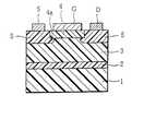
- FIG. 1is a sectional view of an HEMT according to an embodiment of the present invention
- FIG. 2is a sectional view showing a layered structure of the HEMT according to the present invention.
- FIG. 3is a sectional view of the layered structure of FIG. 2 where an SiO 2 film mask has been formed
- FIG. 4is a sectional view of the layered structure of FIG. 3 after a dry etching has been performed.
- FIG. 5is a sectional view of the layered structure of FIG. 4 after an n-type GaN layer has been formed.
- FIG. 1The basic structure of an HEMT according to the present invention is described below referring to FIG. 1.
- FIG. 1One example of the HEMT of the present invention is shown in FIG. 1.
- a layered structure of the HEMT shownis formed by a combination of an epitaxial crystal growth method such as the MOCVD and MBE methods, and photolithography. Initially, a buffer layer 2 is formed on a semi-insulating substrate 1 , and then an undoped GaN layer 3 to be described later is formed on the buffer layer 2 .
- an undoped AlGaN layer 4On the undoped GaN layer 3 is disposed an undoped AlGaN layer 4 via a heterojunction.
- An undercut portion 4 ais formed between a lower face on each side of the undoped AlGaN layer 4 and the undoped GaN layer 3 .
- An n-type GaN layers 5 , 5are formed on the undoped GaN layer 3 in such a manner as to bury both sides of the undoped AlGaN layer 4 and the undercut portion 4 a.
- the semi-insulating substrate 1is preferably made of a material which is in lattice alignment with the respective semiconductor materials successively undergone layer formation thereon.
- the material for the substratemay be a semi-insulating material such as a single crystal of Si or sapphire, for example.
- the material for the buffer layer 2GaN is usually selected.
- a two-dimensional electron gas layeris formed at an upper-most layer portion of the undoped GaN layer 3 during operation, which results in high mobility of electrons.
- the electric resistivity of the undoped GaN layer 3is made not less than 1 ⁇ 10 6 ⁇ /cm 2 , so that a pinch-off state can be realized when the gate bias voltage is set at zero.
- the undoped GaN layer 3 with such a high resistancecan be formed as follows. Specifically, a p-type impurity such as C or Mg is doped simultaneously during the formation of the undoped GaN layer. By so doing, the aforementioned remaining n-type impurity (lattice defect) caused during the formation of the undoped GaN layer can be compensated, whereby the effective carrier concentration in the undoped GaN layer decreases.
- concentration of the remaining n-type impurity in the undoped GaN layervaries depending on the crystal growth method employed and its growth conditions; Normally, however, it is in the range from 5 ⁇ 10 16 to 5 ⁇ 10 15 cm ⁇ 3 .
- the electric resistivity of the resultant undoped GaN layercan be made 1 ⁇ 10 6 ⁇ /cm 2 or more.
- the p-type impuritymay be doped into the undoped GaN layer 3 such that the concentration of the p-type impurity at the upper-most layer portion adjacent the junction interface with the undoped AlGaN layer is one-order or more of magnitude higher than that of the remaining n-type impurity.
- the supply of electrons from the undoped AlGaN layer 4can be reliably prevented, which is very effective in realizing the pinch-off state.
- the above-described HEMTcan be produced by the following manner.
- a slab-layered structureis formed by successively forming on the substrate 1 the buffer layer 2 , the undoped GaN layer 3 and the undoped AlGaN layer 4 .
- Cis doped, for example, to compensate the remaining n-type impurity.
- an SiO 2 filmfor example, is formed on the entire surface of the undoped AlGaN layer 4 . Thereafter, the SiO 2 film is removed except for a portion 6 where the gate electrode is to be formed, whereby the undoped AlGaN layer 4 is exposed (FIG. 3).
- a dry etching such as plasma etchingis then performed by using the SiO 2 film 6 as a mask, thereby removing the exposed undoped AlGaN layer 4 and a part of the undoped GaN layer 3 below (FIG. 4). At this time, the etching conditions are controlled such that an undercut portion 4 a is formed between the undoped GaN layer 3 and the undoped AlGaN layer 4 .
- a selective growth methodfor example, is used to form the n-type GaN layer on the exposed undoped GaN layer 3 , using Si, for example, as the n-type impurity.
- the undercut portion 4 ais buried by the n-type GaN (FIG. 5).
- the undercut portion 4 ais provided so that a good electric conduction can be obtained between the two-dimensional electron gas layer, which is generated at the junction interface between the undoped GaN layer 3 and the undoped AlGaN layer 4 , and the n-type GaN layer 5 .
- SiO 2 film 6 on the undoped AlGaN layer 4is then removed, and an SiO 2 film is newly provided over the entire surface. This is followed by the formation of the electrodes, as described below.
- Photolithography and etchingare used in combination to remove portions of the SiO 2 film where the source and drain electrodes are to be formed, thereby forming openings exposing the n-type GaN layer 5 .
- Alfor example, is then vapor deposited on the e-type GaN layer 5 exposing from these openings to form the source electrode S and the drain electrode D.
- the SiO 2 filmis then removed and an SiO 2 film is again formed on the entire surface.
- a portion of the SiO 2 film where the gate electrode is to be formedis removed by photolithography and etching, thereby forming an opening exposing the undoped AlGaN layer 4 .
- Aufor example, is then vapor deposited there to form the gate electrode G, thereby producing the HEMT as shown in FIG. 1.
- a gas source MBEwas performed to form a GaN buffer layer 2 with a thickness of 50 nm on an Si single crystal substrate 1 at a growth temperature of 640° C.
- Metal Ga(5 ⁇ 10 ⁇ 7 Torr) was used as a Ga source and dimethylhydrazine (5 ⁇ 10 ⁇ 5 Torr) as an N source.
- the N sourcewas switched to ammonia (5 ⁇ 10 ⁇ 5 Torr), and a gas source MBE was performed at a growth temperature of 780° C., thereby forming an undoped GaN layer 3 with a thickness of 2000 nm.
- the carrier concentration of the undoped GaN layer 3was controlled to 1 ⁇ 10 15 cm ⁇ 3 by doping a p-type impurity of Mg (1 ⁇ 10 ⁇ 8 Torr).
- metal Al(1 ⁇ 10 ⁇ 7 Torr) was supplied and a gas source MBE was performed at a growth temperature of 850° C. to form an undoped Al 0.2 Ga 0.8 N layer 4 with a thickness of 30 nm, whereby the layered structure was formed as shown in FIG. 2.
- An SiO 2 filmwas then formed over the entire surface of the undoped Al 0.2 Ga 0.8 N layer 4 with the layered structure by a plasma CVD apparatus.
- a patterning processwas then effected to remove the SiO 2 film except where the gate electrode was to be formed. This was followed by a dry etching process using plasma, thereby forming the layered structure as shown in FIG. 4.
- a portion of the undoped GaN layer 3was removed to a depth of 40 nm below the junction interface with the undoped AlGaN layer 4 .
- an undercut portion 4 awas formed, extending about 20 nm inwardly from both sides of the undoped AlGaN layer 4 .
- a selective growthwas effected by using metal Ga (5 ⁇ 10 ⁇ 7 Torr) as a Ga source, ammonia (5 ⁇ 10 ⁇ 6 Torr) as an N source and Si (5 ⁇ 10 ⁇ 8 Torr) as an n-type impurity, thereby burying the undercut portion 4 a and forming an n-type GaN layer 5 with a thickness of 40 nm, as shown in FIG. 5.
- the Si concentration in the n-type GaN layerwas 2 ⁇ 10 19 cm ⁇ 3 .
- the SiO 2 film on the undoped AlGaN layer 4was then removed by etching using hydrofluoric acid, and again an SiO 2 film was formed on the entire surface by a plasma CVD method.
- a patterning processwas performed to form openings to expose the surface of the n-type GaN layer 5 where the source and drain electrodes were to be formed, while using as a mask the portion of the SiO 2 film where the gate electrode was to be formed.
- Alwas vapor deposited on the surface of the n-type GaN layer 5 exposing from openings to form the source electrode S and the drain electrode D.
- the portion of the SiO 2 film where the gate electrode was to be formedhad a thickness of 100 nm.
- the SiO 2 filmwas then removed by etching with hydrofluoric acid, and an SiO 2 film was again formed on the entire surface. An opening was then formed to expose the surface of the undoped AlGaN layer 4 where the gate electrode was to be formed. Al was then vapor deposited on the exposed surface to form the gate electrode G, thereby producing the HEMT as shown in FIG. 1.
- the layered structurewas formed by gas source MBE, an MOCVD method may also be used. Further, while the film forming of the n-type GaN layer 5 was effected by the selective growth method, Si may be ion-implanted into the undoped GaN layer to thereby obtain an n-type region with a low resistance.
- Mgwas used as the p-type impurity in the undoped GaN layer
- other impuritiessuch as carbon (C), Zn, Be and Cd, or their combinations may be used instead.
- the doping concentration of the p-type impuritymay be selected from a wide range of 5 ⁇ 10 16 cm ⁇ 3 to 1 ⁇ 10 21 cm ⁇ 3 , depending on the quality of the undoped GaN crystal.
- the supply of the p-type impuritymay be terminated prior to the completion of the formation of the GaN layer so that an upper-most portion of the GaN layer with a depth of 5 to 10 nm is undoped and the AlGaN layer may be formed thereon.
- the undoped AlGaN layer 4had the composition Al 0.2 Ga 0.8 N, it may have a general composition of Al x G 1 ⁇ x N (0 ⁇ x ⁇ 1.0).
- the gate electrode Gmay be formed after forming a thin layer of InGaN or GaN on the undoped AlGaN layer 4 .
- the GaN-based HEMT of the present inventioncan realize the pinch-off state even when the gate bias voltage is zero. This is because of the doping of the p-type impurity during the layer formation of the undoped GaN layer.
- the p-type impuritythus doped compensates the great amount of the remaining n-type impurity, i.e., lattice defects, that arises during the formation of the undoped GaN layer in which a two-dimensional electron gas layer is formed.
- the resultant undoped GaN layerhas an electric resistivity of not less than 1 ⁇ 10 6 ⁇ /cm 2 .
Landscapes
- Junction Field-Effect Transistors (AREA)
- Physical Deposition Of Substances That Are Components Of Semiconductor Devices (AREA)
Abstract
Description
- 1. Field of the Invention[0001]
- The present invention relates to a high electron mobility transistor (HEMT) manufactured by using a GaN-based compound semiconductor. More particularly, it relates to a GaN-based HEMT comprising an undoped GaN layer forming a channel, wherein the undoped GaN layer is highly purified or remaining n-type impurities in the GaN layer caused by lattice defects during layer formation are compensated by a p-type impurity, thereby providing the channel with a high electric resistivity and enabling a pinch-off state to be realized when the gate bias voltage is set to zero volt.[0002]
- 2. Prior Art[0003]
- There is an expectation for the HEMT as a high-output microwave device, for example. The HEMTs are manufactured by using mainly a GaAs-based compound semiconductor today.[0004]
- However, the HEMT using the GaAs-based compound semiconductor does not have so high dielectric-breakdown electric field value at the heterojunction interface. Thus, the GaAs-based HEMT has difficulty in realization of high speed operation by the application of a high voltage to the gate electrode.[0005]
- In view of this, recently, attention has been focused on an HEMT using a GaN-based compound semiconductor which has a higher potential (about 2.6 times) of hetero barrier at the heterojunction interface and a larger (by about an order of magnitude) dielectric breakdown electric field value, than the GaAs-based compound semiconductor. The GaN-based HEMT also has excellent heat resistance, and trial and research for the GaN-based HEMT is under way.[0006]
- For example, the GaN-based HEMT is produced by an MOCVD method as follows.[0007]
- First, a buffer layer made of GaN is formed on a semi-insulating sapphire substrate. Then, an undoped (i-type) GaN layer is formed on the GaN buffer layer, using trimethylgallium as a Ga source and ammonia as an N source. Further, an n-type AlGaN layer is formed on the undoped GaN layer by using trimethylaluminum as an Al source and Si as an n-type impurity. After SiO[0008]2is deposited on the n-type AlGaN layer by a plasma CVD method, conventional photolithography and etching are performed, and thereafter predetermined materials are vapor deposited to form a gate electrode, a source electrode and a drain electrode at predetermined locations.
- In such a layered structure, the portion of the n-type AlGaN layer where the gate electrode is formed functions as a source of electrons to be supplied to the undoped GaN layer located below. The supplied electrons form a two-dimensional electron gas layer at the heterojunction interface between the undoped GaN layer and the n-type AlGaN layer, specifically at an upper most layer portion of the undoped GaN layer. There, the electrons move at high speed, thereby realizing an HEMT operation. To realize the high mobility of the electrons, it is necessary that the undoped GaN layer has as little impurities or lattice defects as possible.[0009]
- However, in the case of the HEMT with the above-described layered structure, usually a great number of lattice defects exist in the undoped GaN layer formed, for example, by the MOCVD method. Particularly, a great number of lattice defects due to dangling bonds of nitrogen atoms are present. These lattice defecte remain as an n-type impurity which functions as a donor impurity (hereafter referred to as remaining n-type impurity). As a result, the formed GaN layer does not have a high resistance and instead exhibits the properties of an n-type semiconductor layer. Specifically, there is obtained a state as if an n-type impurity with a concentration of the order of 1×10[0010]16cm−3were doped, with the resulting electric resistivity of the order of 500 Ω/cm2.
- As this kind of state lowers the electric resistivity of the undoped GaN layer, a problem arises that a pinch-off state cannot be realized even when the gate bias voltage is set at 0 V.[0011]
- Thus, in the conventional GaN-based HEMTs, the n-type impurity is effectively doped in the undoped GaN layer due to the above-mentioned problems arising during the film formation process. As a result, the undoped GaN layer cannot be given a high resistance, preventing a sufficiently high enough electron mobility and making it impossible to realize a pinch-off state even if the gate bias voltage is set at zero.[0012]
- It is therefore an object of the present invention to provide a novel GaN-based HEMT which can solve the above-mentioned problems of the prior art and remove the influence of the remaining n-type impurity, whereby the electric resistivity of the undoped GaN layer can be greatly increased to enable the high mobility of the electrons while making it possible to realize a pinch-off state when the gate bias voltage is set at 0 V.[0013]
- To achieve this objective, the GaN-based HEMT according to the present invention comprises a semi-insulating substrate on which a buffer layer is formed, wherein a layered structure is further formed on the buffer layer, the layered structure comprising:[0014]
- an undoped GaN layer having an electric resistivity of not less than 1×10[0015]6Ω/cm2;
- an undoped AlGaN layer disposed on the undoped GaN layer via a heterojunction with an undercut portion formed therebetween; and[0016]
- an n-type GaN layer disposed in such a manner as to bury side portions of the undoped AlGaN layer and the undercut portion, wherein:[0017]
- a gate electrode is formed on the undoped AlGaN layer, and a source electrode and a drain electrode are formed on the n-type GaN layer.[0018]
- The undoped GaN layer may preferably be formed by doping a p-type impurity during the layer formation process to compensate the remaining n-type impurity.[0019]
- FIG. 1 is a sectional view of an HEMT according to an embodiment of the present invention;[0020]
- FIG. 2 is a sectional view showing a layered structure of the HEMT according to the present invention;[0021]
- FIG. 3 is a sectional view of the layered structure of FIG. 2 where an SiO[0022]2film mask has been formed;
- FIG. 4 is a sectional view of the layered structure of FIG. 3 after a dry etching has been performed; and[0023]
- FIG. 5 is a sectional view of the layered structure of FIG. 4 after an n-type GaN layer has been formed.[0024]
- The basic structure of an HEMT according to the present invention is described below referring to FIG. 1. One example of the HEMT of the present invention is shown in FIG. 1.[0025]
- A layered structure of the HEMT shown is formed by a combination of an epitaxial crystal growth method such as the MOCVD and MBE methods, and photolithography. Initially, a[0026]
buffer layer 2 is formed on asemi-insulating substrate 1, and then anundoped GaN layer 3 to be described later is formed on thebuffer layer 2. - On the undoped GaN[0027]
layer 3 is disposed an undoped AlGaNlayer 4 via a heterojunction. Anundercut portion 4ais formed between a lower face on each side of the undoped AlGaNlayer 4 and theundoped GaN layer 3. An n-type GaN layers undoped GaN layer 3 in such a manner as to bury both sides of the undoped AlGaNlayer 4 and theundercut portion 4a. - A gate electrode G made of Au, for example, is formed on the[0028]
undoped AlGaN layer 4. A source electrode S and a drain electrode D, both made of Al, for example, are formed on the n-type GaN layers undoped AlGaN layer 4. - The[0029]
semi-insulating substrate 1 is preferably made of a material which is in lattice alignment with the respective semiconductor materials successively undergone layer formation thereon. However, there is no such material as far as GaN materials are concerned. Accordingly, the material for the substrate may be a semi-insulating material such as a single crystal of Si or sapphire, for example. As the material for thebuffer layer 2, GaN is usually selected. - In the HEMT with such a layered structure, a two-dimensional electron gas layer is formed at an upper-most layer portion of the[0030]
undoped GaN layer 3 during operation, which results in high mobility of electrons. In the HEMT according to the present invention, the electric resistivity of theundoped GaN layer 3 is made not less than 1×10⁶Ω/cm2, so that a pinch-off state can be realized when the gate bias voltage is set at zero. - The undoped GaN[0031]
layer 3 with such a high resistance can be formed as follows. Specifically, a p-type impurity such as C or Mg is doped simultaneously during the formation of the undoped GaN layer. By so doing, the aforementioned remaining n-type impurity (lattice defect) caused during the formation of the undoped GaN layer can be compensated, whereby the effective carrier concentration in the undoped GaN layer decreases. The concentration of the remaining n-type impurity in the undoped GaN layer varies depending on the crystal growth method employed and its growth conditions; Normally, however, it is in the range from 5×10¹⁶to 5×1015cm−3. Thus, by setting the dope amount of the p-type impurity in the range of 2×10¹⁷to 5×1016cm3, the electric resistivity of the resultant undoped GaN layer can be made 1×10⁶Ω/cm2or more. - The p-type impurity may be doped into the[0032]
undoped GaN layer 3 such that the concentration of the p-type impurity at the upper-most layer portion adjacent the junction interface with the undoped AlGaN layer is one-order or more of magnitude higher than that of the remaining n-type impurity. The supply of electrons from theundoped AlGaN layer 4 can be reliably prevented, which is very effective in realizing the pinch-off state. - The above-described HEMT can be produced by the following manner.[0033]
- As shown in FIG. 2, a slab-layered structure is formed by successively forming on the[0034]
substrate 1 thebuffer layer 2, theundoped GaN layer 3 and theundoped AlGaN layer 4. When theundoped GaN layer 3 is formed, C is doped, for example, to compensate the remaining n-type impurity. - Next, an SiO[0035]2film, for example, is formed on the entire surface of the
undoped AlGaN layer 4. Thereafter, the SiO2film is removed except for aportion 6 where the gate electrode is to be formed, whereby theundoped AlGaN layer 4 is exposed (FIG. 3). - A dry etching such as plasma etching is then performed by using the SiO[0036]2film6 as a mask, thereby removing the exposed
undoped AlGaN layer 4 and a part of theundoped GaN layer 3 below (FIG. 4). At this time, the etching conditions are controlled such that an undercutportion 4ais formed between theundoped GaN layer 3 and theundoped AlGaN layer 4. - Thereafter, a selective growth method, for example, is used to form the n-type GaN layer on the exposed[0037]
undoped GaN layer 3, using Si, for example, as the n-type impurity. Simultaneously, the undercutportion 4ais buried by the n-type GaN (FIG. 5). - The undercut[0038]
portion 4ais provided so that a good electric conduction can be obtained between the two-dimensional electron gas layer, which is generated at the junction interface between theundoped GaN layer 3 and theundoped AlGaN layer 4, and the n-type GaN layer 5. - The SiO[0039]2film6 on the
undoped AlGaN layer 4 is then removed, and an SiO2film is newly provided over the entire surface. This is followed by the formation of the electrodes, as described below. - Photolithography and etching are used in combination to remove portions of the SiO[0040]2film where the source and drain electrodes are to be formed, thereby forming openings exposing the n-
type GaN layer 5. Al, for example, is then vapor deposited on thee-type GaN layer 5 exposing from these openings to form the source electrode S and the drain electrode D. The SiO2film is then removed and an SiO2film is again formed on the entire surface. A portion of the SiO2film where the gate electrode is to be formed is removed by photolithography and etching, thereby forming an opening exposing theundoped AlGaN layer 4. Au, for example, is then vapor deposited there to form the gate electrode G, thereby producing the HEMT as shown in FIG. 1. - By using an ultravacuum apparatus with a growth chamber and a patterning chamber, a gas source MBE was performed to form a[0041]
GaN buffer layer 2 with a thickness of 50 nm on an Sisingle crystal substrate 1 at a growth temperature of 640° C. Metal Ga (5×10⁻⁷Torr) was used as a Ga source and dimethylhydrazine (5×10⁻⁵Torr) as an N source. - Then, the N source was switched to ammonia (5×10[0042]−5Torr), and a gas source MBE was performed at a growth temperature of 780° C., thereby forming an
undoped GaN layer 3 with a thickness of 2000 nm. The carrier concentration of theundoped GaN layer 3 was controlled to 1×1015cm−3by doping a p-type impurity of Mg (1×10⁻⁸Torr). - In a separate experiment, the same undoped GaN layer was formed under the same conditions. When its electric resistivity was measured by a contactless-type contact resistance measurement apparatus, the reading was 100 MΩ/cm[0043]2.
- Thereafter, metal Al (1×10[0044]−7Torr) was supplied and a gas source MBE was performed at a growth temperature of 850° C. to form an undoped Al0.2Ga0.8N layer4 with a thickness of 30 nm, whereby the layered structure was formed as shown in FIG. 2.
- An SiO[0045]2film was then formed over the entire surface of the undoped Al0.2Ga0.8N layer4 with the layered structure by a plasma CVD apparatus. A patterning process was then effected to remove the SiO2film except where the gate electrode was to be formed. This was followed by a dry etching process using plasma, thereby forming the layered structure as shown in FIG. 4. During the etching, a portion of the
undoped GaN layer 3 was removed to a depth of 40 nm below the junction interface with theundoped AlGaN layer 4. At the same time, an undercutportion 4awas formed, extending about 20 nm inwardly from both sides of theundoped AlGaN layer 4. - Thereafter, a selective growth was effected by using metal Ga (5×10[0046]−7Torr) as a Ga source, ammonia (5×10⁻⁶Torr) as an N source and Si (5×10⁻⁸Torr) as an n-type impurity, thereby burying the undercut
portion 4aand forming an n-type GaN layer 5 with a thickness of 40 nm, as shown in FIG. 5. The Si concentration in the n-type GaN layer was 2×1019cm−3. - The SiO[0047]2film on the
undoped AlGaN layer 4 was then removed by etching using hydrofluoric acid, and again an SiO2film was formed on the entire surface by a plasma CVD method. - Then a patterning process was performed to form openings to expose the surface of the n-[0048]
type GaN layer 5 where the source and drain electrodes were to be formed, while using as a mask the portion of the SiO2film where the gate electrode was to be formed. Al was vapor deposited on the surface of the n-type GaN layer 5 exposing from openings to form the source electrode S and the drain electrode D. The portion of the SiO2film where the gate electrode was to be formed had a thickness of 100 nm. - The SiO[0049]2film was then removed by etching with hydrofluoric acid, and an SiO2film was again formed on the entire surface. An opening was then formed to expose the surface of the
undoped AlGaN layer 4 where the gate electrode was to be formed. Al was then vapor deposited on the exposed surface to form the gate electrode G, thereby producing the HEMT as shown in FIG. 1. - In this HEMT, Ids remained 0 mA/mm when the gate bias voltage was set at 0 V and Vds was varied. When Vgs was set at +3V, the HEMT indicated an Ids of 500 mA/mm.[0050]
- While in the above example, the layered structure was formed by gas source MBE, an MOCVD method may also be used. Further, while the film forming of the n-[0051]
type GaN layer 5 was effected by the selective growth method, Si may be ion-implanted into the undoped GaN layer to thereby obtain an n-type region with a low resistance. - While Mg was used as the p-type impurity in the undoped GaN layer, other impurities such as carbon (C), Zn, Be and Cd, or their combinations may be used instead.[0052]
- The doping concentration of the p-type impurity may be selected from a wide range of 5×10[0053]16cm−3to 1×1021cm−3, depending on the quality of the undoped GaN crystal.
- If the p-type impurity diffuses into the AlGaN layer, the supply of the p-type impurity may be terminated prior to the completion of the formation of the GaN layer so that an upper-most portion of the GaN layer with a depth of 5 to 10 nm is undoped and the AlGaN layer may be formed thereon.[0054]
- Furthermore, while the[0055]
undoped AlGaN layer 4 had the composition Al0.2Ga0.8N, it may have a general composition of AlxG1−xN (0≦x≦1.0). - In order to obtain a better contact between the gate electrode G and the[0056]
undoped AlGaN layer 4, the gate electrode G may be formed after forming a thin layer of InGaN or GaN on theundoped AlGaN layer 4. - As is apparent from the foregoing description, the GaN-based HEMT of the present invention can realize the pinch-off state even when the gate bias voltage is zero. This is because of the doping of the p-type impurity during the layer formation of the undoped GaN layer. The p-type impurity thus doped compensates the great amount of the remaining n-type impurity, i.e., lattice defects, that arises during the formation of the undoped GaN layer in which a two-dimensional electron gas layer is formed. As a result of the compensation, the resultant undoped GaN layer has an electric resistivity of not less than 1×10[0057]6Ω/cm2.
Claims (3)
1. A GaN-based high electron mobility transistor comprising a semi-insulating substrate on which a buffer layer is formed, wherein a layered structure is further formed on the buffer layer, the layered structure comprising:
an undoped GaN layer having an electric resistivity of not less than 1×10⁶Ω/cm2;
an undoped AlGaN layer disposed on the undoped GaN layer via a heterojunction with an undercut portion formed therebetween; and
an n-type GaN layer disposed in such a manner as to bury side portions of the undoped AlGaN layer and the undercut portion, wherein:
a gate electrode is formed on the undoped AlGaN layer, and a source electrode and a drain electrode are formed on the n-type GaN layer.
2. The GaN-based high electron mobility transistor according toclaim 1 , wherein the undoped GaN layer is doped with a p-type impurity.
3. The GaN-based high electron mobility transistor according toclaim 2 , wherein the p-type impurity is selected from the group consisting of C, Mg, Si, Zn, Be and Cd.
Applications Claiming Priority (2)
| Application Number | Priority Date | Filing Date | Title |
|---|---|---|---|
| JP2000385219AJP3428962B2 (en) | 2000-12-19 | 2000-12-19 | GaN based high mobility transistor |
| JP2000-385219 | 2000-12-19 |
Publications (2)
| Publication Number | Publication Date |
|---|---|
| US20020079508A1true US20020079508A1 (en) | 2002-06-27 |
| US6534801B2 US6534801B2 (en) | 2003-03-18 |
Family
ID=18852525
Family Applications (1)
| Application Number | Title | Priority Date | Filing Date |
|---|---|---|---|
| US10/017,593Expired - LifetimeUS6534801B2 (en) | 2000-12-19 | 2001-12-18 | GaN-based high electron mobility transistor |
Country Status (2)
| Country | Link |
|---|---|
| US (1) | US6534801B2 (en) |
| JP (1) | JP3428962B2 (en) |
Cited By (45)
| Publication number | Priority date | Publication date | Assignee | Title |
|---|---|---|---|---|
| US20030102482A1 (en)* | 2001-12-03 | 2003-06-05 | Saxler Adam William | Strain balanced nitride heterojunction transistors and methods of fabricating strain balanced nitride heterojunction transistors |
| US20030106490A1 (en)* | 2001-12-06 | 2003-06-12 | Applied Materials, Inc. | Apparatus and method for fast-cycle atomic layer deposition |
| US20030160269A1 (en)* | 2002-02-28 | 2003-08-28 | Matsushita Electric Industrial Co., Ltd. | Semiconductor device and method for fabricating the same |
| US20050009221A1 (en)* | 2003-06-23 | 2005-01-13 | Ngk Insulators, Ltd. | Method for manufacturing nitride film including high-resistivity GaN layer and epitaxial substrate manufactured by the method |
| US20050170574A1 (en)* | 2004-01-16 | 2005-08-04 | Sheppard Scott T. | Nitride-based transistors with a protective layer and a low-damage recess and methods of fabrication thereof |
| US20050173728A1 (en)* | 2004-02-05 | 2005-08-11 | Saxler Adam W. | Nitride heterojunction transistors having charge-transfer induced energy barriers and methods of fabricating the same |
| US20050258451A1 (en)* | 2004-05-20 | 2005-11-24 | Saxler Adam W | Methods of fabricating nitride-based transistors having regrown ohmic contact regions and nitride-based transistors having regrown ohmic contact regions |
| US20050258450A1 (en)* | 2004-05-20 | 2005-11-24 | Saxler Adam W | Semiconductor devices having a hybrid channel layer, current aperture transistors and methods of fabricating same |
| US20060017064A1 (en)* | 2004-07-26 | 2006-01-26 | Saxler Adam W | Nitride-based transistors having laterally grown active region and methods of fabricating same |
| US20060108606A1 (en)* | 2004-11-23 | 2006-05-25 | Saxler Adam W | Cap layers and/or passivation layers for nitride-based transistors, transistor structures and methods of fabricating same |
| US20060208280A1 (en)* | 2005-03-15 | 2006-09-21 | Smith Richard P | Group III nitride field effect transistors (FETS) capable of withstanding high temperature reverse bias test conditions |
| US20060226413A1 (en)* | 2005-04-11 | 2006-10-12 | Saxler Adam W | Composite substrates of conductive and insulating or semi-insulating group III-nitrides for group III-nitride devices |
| US20060226412A1 (en)* | 2005-04-11 | 2006-10-12 | Saxler Adam W | Thick semi-insulating or insulating epitaxial gallium nitride layers and devices incorporating same |
| US20060244010A1 (en)* | 2005-04-29 | 2006-11-02 | Saxler Adam W | Aluminum free group III-nitride based high electron mobility transistors and methods of fabricating same |
| US20060244011A1 (en)* | 2005-04-29 | 2006-11-02 | Saxler Adam W | Binary group III-nitride based high electron mobility transistors and methods of fabricating same |
| US20060255364A1 (en)* | 2004-02-05 | 2006-11-16 | Saxler Adam W | Heterojunction transistors including energy barriers and related methods |
| US20070004184A1 (en)* | 2005-06-29 | 2007-01-04 | Saxler Adam W | Low dislocation density group III nitride layers on silicon carbide substrates and methods of making the same |
| US7161194B2 (en) | 2004-12-06 | 2007-01-09 | Cree, Inc. | High power density and/or linearity transistors |
| US20070018198A1 (en)* | 2005-07-20 | 2007-01-25 | Brandes George R | High electron mobility electronic device structures comprising native substrates and methods for making the same |
| US20070164315A1 (en)* | 2004-11-23 | 2007-07-19 | Cree, Inc. | Cap Layers Including Aluminum Nitride for Nitride-Based Transistors and Methods of Fabricating Same |
| US20070218611A1 (en)* | 2006-03-14 | 2007-09-20 | Northrop Grumman Corporation | Leakage barrier for GaN based HEMT active device |
| US20080315210A1 (en)* | 2007-06-15 | 2008-12-25 | Rohm Co., Ltd. | High electron mobility transistor |
| US20100068855A1 (en)* | 2004-01-16 | 2010-03-18 | Cree, Inc. | Group III nitride semiconductor devices with silicon nitride layers and methods of manufacturing such devices |
| US20110233712A1 (en)* | 2005-06-15 | 2011-09-29 | Panasonic Corporation | Semiconductor device and method for fabricating the same |
| US20140054602A1 (en)* | 2012-08-27 | 2014-02-27 | Rf Micro Devices, Inc. | Field effect transistor (fet) having fingers with rippled edges |
| CN103903982A (en)* | 2014-03-21 | 2014-07-02 | 中国电子科技集团公司第十三研究所 | Method for reducing ohmic contact resistance of HEMT device |
| US8823057B2 (en) | 2006-11-06 | 2014-09-02 | Cree, Inc. | Semiconductor devices including implanted regions for providing low-resistance contact to buried layers and related devices |
| US8988097B2 (en) | 2012-08-24 | 2015-03-24 | Rf Micro Devices, Inc. | Method for on-wafer high voltage testing of semiconductor devices |
| US9093420B2 (en) | 2012-04-18 | 2015-07-28 | Rf Micro Devices, Inc. | Methods for fabricating high voltage field effect transistor finger terminations |
| US9123740B2 (en) | 2012-01-11 | 2015-09-01 | Samsung Electronics Co., Ltd. | High electron mobility transistors and methods of manufacturing the same |
| US9124221B2 (en) | 2012-07-16 | 2015-09-01 | Rf Micro Devices, Inc. | Wide bandwidth radio frequency amplier having dual gate transistors |
| US9129802B2 (en) | 2012-08-27 | 2015-09-08 | Rf Micro Devices, Inc. | Lateral semiconductor device with vertical breakdown region |
| US9142620B2 (en) | 2012-08-24 | 2015-09-22 | Rf Micro Devices, Inc. | Power device packaging having backmetals couple the plurality of bond pads to the die backside |
| US9147632B2 (en) | 2012-08-24 | 2015-09-29 | Rf Micro Devices, Inc. | Semiconductor device having improved heat dissipation |
| US9202874B2 (en) | 2012-08-24 | 2015-12-01 | Rf Micro Devices, Inc. | Gallium nitride (GaN) device with leakage current-based over-voltage protection |
| US9299800B2 (en) | 2010-10-06 | 2016-03-29 | Samsun Electronics Co., Ltd. | Methods of manufacturing high electron mobility transistors |
| US9325281B2 (en) | 2012-10-30 | 2016-04-26 | Rf Micro Devices, Inc. | Power amplifier controller |
| US9455327B2 (en) | 2014-06-06 | 2016-09-27 | Qorvo Us, Inc. | Schottky gated transistor with interfacial layer |
| US9496197B1 (en)* | 2012-04-20 | 2016-11-15 | Hrl Laboratories, Llc | Near junction cooling for GaN devices |
| US9536803B2 (en) | 2014-09-05 | 2017-01-03 | Qorvo Us, Inc. | Integrated power module with improved isolation and thermal conductivity |
| US9917080B2 (en) | 2012-08-24 | 2018-03-13 | Qorvo US. Inc. | Semiconductor device with electrical overstress (EOS) protection |
| US10062684B2 (en) | 2015-02-04 | 2018-08-28 | Qorvo Us, Inc. | Transition frequency multiplier semiconductor device |
| US10615158B2 (en) | 2015-02-04 | 2020-04-07 | Qorvo Us, Inc. | Transition frequency multiplier semiconductor device |
| WO2020106658A1 (en)* | 2018-11-19 | 2020-05-28 | Texas Instruments Incorporated | Gallium nitride transistor with a doped region |
| DE112010001589B4 (en) | 2009-04-08 | 2024-11-28 | Efficient Power Conversion Corporation | Compensated GATE-MISFET |
Families Citing this family (26)
| Publication number | Priority date | Publication date | Assignee | Title |
|---|---|---|---|---|
| GB2392170A (en) | 2002-08-23 | 2004-02-25 | Sharp Kk | MBE growth of a semiconductor layer structure |
| JP4748498B2 (en)* | 2002-12-05 | 2011-08-17 | 古河電気工業株式会社 | GaN-based semiconductor device with current breaker |
| JP4142429B2 (en)* | 2002-12-26 | 2008-09-03 | 古河電気工業株式会社 | Current detection circuit |
| JP2004289005A (en)* | 2003-03-24 | 2004-10-14 | Ngk Insulators Ltd | Epitaxial substrate, semiconductor device, and high electron mobility transistor |
| CN100466178C (en)* | 2003-12-26 | 2009-03-04 | 松下电器产业株式会社 | Method for producing group III nitride crystal, group III nitride crystal obtained thereby, and group III nitride crystal substrate using same |
| JP4398780B2 (en)* | 2004-04-30 | 2010-01-13 | 古河電気工業株式会社 | GaN-based semiconductor device |
| JP2006086354A (en) | 2004-09-16 | 2006-03-30 | Toshiba Corp | Nitride semiconductor device |
| US7834380B2 (en) | 2004-12-09 | 2010-11-16 | Panasonic Corporation | Field effect transistor and method for fabricating the same |
| US7326971B2 (en)* | 2005-06-08 | 2008-02-05 | Cree, Inc. | Gallium nitride based high-electron mobility devices |
| US7364988B2 (en)* | 2005-06-08 | 2008-04-29 | Cree, Inc. | Method of manufacturing gallium nitride based high-electron mobility devices |
| US7485512B2 (en)* | 2005-06-08 | 2009-02-03 | Cree, Inc. | Method of manufacturing an adaptive AIGaN buffer layer |
| JP4531071B2 (en) | 2007-02-20 | 2010-08-25 | 富士通株式会社 | Compound semiconductor device |
| JP5044489B2 (en)* | 2007-08-28 | 2012-10-10 | 日本碍子株式会社 | Hall element, Hall IC, and method of manufacturing Hall element |
| US7875537B2 (en)* | 2007-08-29 | 2011-01-25 | Cree, Inc. | High temperature ion implantation of nitride based HEMTs |
| EP2040299A1 (en)* | 2007-09-12 | 2009-03-25 | Forschungsverbund Berlin e.V. | Electrical devices having improved transfer characteristics and method for tailoring the transfer characteristics of such an electrical device |
| WO2009039298A2 (en)* | 2007-09-18 | 2009-03-26 | University Of Florida Research Foundation, Inc. | Sensors using aigan/gan high electron mobility transistors |
| US8836351B2 (en)* | 2008-06-10 | 2014-09-16 | University Of Florida Research Foundation, Inc. | Chloride detection |
| WO2010054159A2 (en) | 2008-11-06 | 2010-05-14 | University Of Florida Research Foundation, Inc. | Materials and methods for detecting toxins, pathogens and other biological materials |
| US8592865B1 (en) | 2009-10-29 | 2013-11-26 | Hrl Laboratories, Llc | Overvoltage tolerant HFETs |
| JP5455875B2 (en)* | 2010-11-25 | 2014-03-26 | 日本碍子株式会社 | Epitaxial substrate manufacturing method |
| JP5775321B2 (en) | 2011-02-17 | 2015-09-09 | トランスフォーム・ジャパン株式会社 | Semiconductor device, manufacturing method thereof, and power supply device |
| JP5848680B2 (en) | 2011-11-22 | 2016-01-27 | ルネサスエレクトロニクス株式会社 | Semiconductor device and manufacturing method of semiconductor device |
| US9666683B2 (en) | 2015-10-09 | 2017-05-30 | Taiwan Semiconductor Manufacturing Company, Ltd. | Surface treatment and passivation for high electron mobility transistors |
| US11101378B2 (en) | 2019-04-09 | 2021-08-24 | Raytheon Company | Semiconductor structure having both enhancement mode group III-N high electron mobility transistors and depletion mode group III-N high electron mobility transistors |
| US11545566B2 (en)* | 2019-12-26 | 2023-01-03 | Raytheon Company | Gallium nitride high electron mobility transistors (HEMTs) having reduced current collapse and power added efficiency enhancement |
| US11362190B2 (en) | 2020-05-22 | 2022-06-14 | Raytheon Company | Depletion mode high electron mobility field effect transistor (HEMT) semiconductor device having beryllium doped Schottky contact layers |
Family Cites Families (4)
| Publication number | Priority date | Publication date | Assignee | Title |
|---|---|---|---|---|
| US5679152A (en)* | 1994-01-27 | 1997-10-21 | Advanced Technology Materials, Inc. | Method of making a single crystals Ga*N article |
| JP3372470B2 (en)* | 1998-01-20 | 2003-02-04 | シャープ株式会社 | Nitride III-V compound semiconductor device |
| JP3439111B2 (en)* | 1998-03-09 | 2003-08-25 | 古河電気工業株式会社 | High mobility transistor |
| US6586781B2 (en)* | 2000-02-04 | 2003-07-01 | Cree Lighting Company | Group III nitride based FETs and HEMTs with reduced trapping and method for producing the same |
- 2000
- 2000-12-19JPJP2000385219Apatent/JP3428962B2/ennot_activeExpired - Lifetime
- 2001
- 2001-12-18USUS10/017,593patent/US6534801B2/ennot_activeExpired - Lifetime
Cited By (96)
| Publication number | Priority date | Publication date | Assignee | Title |
|---|---|---|---|---|
| US7030428B2 (en) | 2001-12-03 | 2006-04-18 | Cree, Inc. | Strain balanced nitride heterojunction transistors |
| US20030102482A1 (en)* | 2001-12-03 | 2003-06-05 | Saxler Adam William | Strain balanced nitride heterojunction transistors and methods of fabricating strain balanced nitride heterojunction transistors |
| US8153515B2 (en) | 2001-12-03 | 2012-04-10 | Cree, Inc. | Methods of fabricating strain balanced nitride heterojunction transistors |
| US20060121682A1 (en)* | 2001-12-03 | 2006-06-08 | Cree, Inc. | Strain balanced nitride heterojunction transistors and methods of fabricating strain balanced nitride heterojunction transistors |
| US20030106490A1 (en)* | 2001-12-06 | 2003-06-12 | Applied Materials, Inc. | Apparatus and method for fast-cycle atomic layer deposition |
| US6773507B2 (en) | 2001-12-06 | 2004-08-10 | Applied Materials, Inc. | Apparatus and method for fast-cycle atomic layer deposition |
| US20030160269A1 (en)* | 2002-02-28 | 2003-08-28 | Matsushita Electric Industrial Co., Ltd. | Semiconductor device and method for fabricating the same |
| US6737683B2 (en)* | 2002-02-28 | 2004-05-18 | Matsushita Electric Industrial Co., Ltd. | Semiconductor device composed of a group III-V nitride semiconductor |
| US7122451B2 (en) | 2002-02-28 | 2006-10-17 | Matsushita Electric Industrial Co., Ltd. | Method for fabricating a semiconductor device including exposing a group III-V semiconductor to an ammonia plasma |
| US20070020896A1 (en)* | 2002-02-28 | 2007-01-25 | Matsushita Electric Industrial Co., Ltd. | Semiconductor device and method for fabricating the same |
| US7449399B2 (en) | 2002-02-28 | 2008-11-11 | Matsushita Electric Industrial Co., Ltd. | Method for fabricating a semiconductor device for reducing a surface potential |
| US20050009221A1 (en)* | 2003-06-23 | 2005-01-13 | Ngk Insulators, Ltd. | Method for manufacturing nitride film including high-resistivity GaN layer and epitaxial substrate manufactured by the method |
| US7135347B2 (en)* | 2003-06-23 | 2006-11-14 | Ngk Insulators, Ltd. | Method for manufacturing nitride film including high-resistivity GaN layer and epitaxial substrate manufactured by the method |
| US20110136305A1 (en)* | 2004-01-16 | 2011-06-09 | Adam William Saxler | Group III Nitride Semiconductor Devices with Silicon Nitride Layers and Methods of Manufacturing Such Devices |
| US7045404B2 (en) | 2004-01-16 | 2006-05-16 | Cree, Inc. | Nitride-based transistors with a protective layer and a low-damage recess and methods of fabrication thereof |
| US7906799B2 (en) | 2004-01-16 | 2011-03-15 | Cree, Inc. | Nitride-based transistors with a protective layer and a low-damage recess |
| US20110140123A1 (en)* | 2004-01-16 | 2011-06-16 | Sheppard Scott T | Nitride-Based Transistors With a Protective Layer and a Low-Damage Recess |
| US7901994B2 (en) | 2004-01-16 | 2011-03-08 | Cree, Inc. | Methods of manufacturing group III nitride semiconductor devices with silicon nitride layers |
| US20100068855A1 (en)* | 2004-01-16 | 2010-03-18 | Cree, Inc. | Group III nitride semiconductor devices with silicon nitride layers and methods of manufacturing such devices |
| US8481376B2 (en) | 2004-01-16 | 2013-07-09 | Cree, Inc. | Group III nitride semiconductor devices with silicon nitride layers and methods of manufacturing such devices |
| US11316028B2 (en) | 2004-01-16 | 2022-04-26 | Wolfspeed, Inc. | Nitride-based transistors with a protective layer and a low-damage recess |
| US20050170574A1 (en)* | 2004-01-16 | 2005-08-04 | Sheppard Scott T. | Nitride-based transistors with a protective layer and a low-damage recess and methods of fabrication thereof |
| US20060255364A1 (en)* | 2004-02-05 | 2006-11-16 | Saxler Adam W | Heterojunction transistors including energy barriers and related methods |
| US7170111B2 (en) | 2004-02-05 | 2007-01-30 | Cree, Inc. | Nitride heterojunction transistors having charge-transfer induced energy barriers and methods of fabricating the same |
| US9035354B2 (en) | 2004-02-05 | 2015-05-19 | Cree, Inc. | Heterojunction transistors having barrier layer bandgaps greater than channel layer bandgaps and related methods |
| US7612390B2 (en) | 2004-02-05 | 2009-11-03 | Cree, Inc. | Heterojunction transistors including energy barriers |
| US20100187570A1 (en)* | 2004-02-05 | 2010-07-29 | Adam William Saxler | Heterojunction Transistors Having Barrier Layer Bandgaps Greater Than Channel Layer Bandgaps and Related Methods |
| US20050173728A1 (en)* | 2004-02-05 | 2005-08-11 | Saxler Adam W. | Nitride heterojunction transistors having charge-transfer induced energy barriers and methods of fabricating the same |
| US7432142B2 (en) | 2004-05-20 | 2008-10-07 | Cree, Inc. | Methods of fabricating nitride-based transistors having regrown ohmic contact regions |
| US7479669B2 (en) | 2004-05-20 | 2009-01-20 | Cree, Inc. | Current aperture transistors and methods of fabricating same |
| US20050258451A1 (en)* | 2004-05-20 | 2005-11-24 | Saxler Adam W | Methods of fabricating nitride-based transistors having regrown ohmic contact regions and nitride-based transistors having regrown ohmic contact regions |
| US20050258450A1 (en)* | 2004-05-20 | 2005-11-24 | Saxler Adam W | Semiconductor devices having a hybrid channel layer, current aperture transistors and methods of fabricating same |
| WO2005119787A1 (en)* | 2004-05-20 | 2005-12-15 | Cree, Inc. | Methods of fabricating nitride-based transistors having regrown ohmic contact regions and nitride-based transistors having regrown ohmic contact regions |
| US7084441B2 (en) | 2004-05-20 | 2006-08-01 | Cree, Inc. | Semiconductor devices having a hybrid channel layer, current aperture transistors and methods of fabricating same |
| US20060017064A1 (en)* | 2004-07-26 | 2006-01-26 | Saxler Adam W | Nitride-based transistors having laterally grown active region and methods of fabricating same |
| US20100012952A1 (en)* | 2004-07-26 | 2010-01-21 | Adam William Saxler | Nitride-Based Transistors Having Laterally Grown Active Region and Methods of Fabricating Same |
| US8946777B2 (en) | 2004-07-26 | 2015-02-03 | Cree, Inc. | Nitride-based transistors having laterally grown active region and methods of fabricating same |
| US7456443B2 (en) | 2004-11-23 | 2008-11-25 | Cree, Inc. | Transistors having buried n-type and p-type regions beneath the source region |
| US20060108606A1 (en)* | 2004-11-23 | 2006-05-25 | Saxler Adam W | Cap layers and/or passivation layers for nitride-based transistors, transistor structures and methods of fabricating same |
| US20070164315A1 (en)* | 2004-11-23 | 2007-07-19 | Cree, Inc. | Cap Layers Including Aluminum Nitride for Nitride-Based Transistors and Methods of Fabricating Same |
| US20090042345A1 (en)* | 2004-11-23 | 2009-02-12 | Cree, Inc. | Methods of Fabricating Transistors Having Buried N-Type and P-Type Regions Beneath the Source Region |
| US7709859B2 (en) | 2004-11-23 | 2010-05-04 | Cree, Inc. | Cap layers including aluminum nitride for nitride-based transistors |
| US9166033B2 (en) | 2004-11-23 | 2015-10-20 | Cree, Inc. | Methods of passivating surfaces of wide bandgap semiconductor devices |
| US7161194B2 (en) | 2004-12-06 | 2007-01-09 | Cree, Inc. | High power density and/or linearity transistors |
| US20060208280A1 (en)* | 2005-03-15 | 2006-09-21 | Smith Richard P | Group III nitride field effect transistors (FETS) capable of withstanding high temperature reverse bias test conditions |
| US7465967B2 (en) | 2005-03-15 | 2008-12-16 | Cree, Inc. | Group III nitride field effect transistors (FETS) capable of withstanding high temperature reverse bias test conditions |
| US8803198B2 (en) | 2005-03-15 | 2014-08-12 | Cree, Inc. | Group III nitride field effect transistors (FETS) capable of withstanding high temperature reverse bias test conditions |
| US8212289B2 (en) | 2005-03-15 | 2012-07-03 | Cree, Inc. | Group III nitride field effect transistors (FETS) capable of withstanding high temperature reverse bias test conditions |
| US8575651B2 (en) | 2005-04-11 | 2013-11-05 | Cree, Inc. | Devices having thick semi-insulating epitaxial gallium nitride layer |
| US9224596B2 (en) | 2005-04-11 | 2015-12-29 | Cree, Inc. | Methods of fabricating thick semi-insulating or insulating epitaxial gallium nitride layers |
| US20060226413A1 (en)* | 2005-04-11 | 2006-10-12 | Saxler Adam W | Composite substrates of conductive and insulating or semi-insulating group III-nitrides for group III-nitride devices |
| US7626217B2 (en) | 2005-04-11 | 2009-12-01 | Cree, Inc. | Composite substrates of conductive and insulating or semi-insulating group III-nitrides for group III-nitride devices |
| US20060226412A1 (en)* | 2005-04-11 | 2006-10-12 | Saxler Adam W | Thick semi-insulating or insulating epitaxial gallium nitride layers and devices incorporating same |
| US20060244011A1 (en)* | 2005-04-29 | 2006-11-02 | Saxler Adam W | Binary group III-nitride based high electron mobility transistors and methods of fabricating same |
| US7544963B2 (en) | 2005-04-29 | 2009-06-09 | Cree, Inc. | Binary group III-nitride based high electron mobility transistors |
| US20060244010A1 (en)* | 2005-04-29 | 2006-11-02 | Saxler Adam W | Aluminum free group III-nitride based high electron mobility transistors and methods of fabricating same |
| US7615774B2 (en) | 2005-04-29 | 2009-11-10 | Cree.Inc. | Aluminum free group III-nitride based high electron mobility transistors |
| US20110233712A1 (en)* | 2005-06-15 | 2011-09-29 | Panasonic Corporation | Semiconductor device and method for fabricating the same |
| US9331192B2 (en) | 2005-06-29 | 2016-05-03 | Cree, Inc. | Low dislocation density group III nitride layers on silicon carbide substrates and methods of making the same |
| US20070004184A1 (en)* | 2005-06-29 | 2007-01-04 | Saxler Adam W | Low dislocation density group III nitride layers on silicon carbide substrates and methods of making the same |
| US20070018198A1 (en)* | 2005-07-20 | 2007-01-25 | Brandes George R | High electron mobility electronic device structures comprising native substrates and methods for making the same |
| US20080153215A1 (en)* | 2006-03-14 | 2008-06-26 | Rajinder Randy Sandhu | LEAKAGE BARRIER FOR GaN BASED HEMT ACTIVE DEVICE |
| US8809137B2 (en) | 2006-03-14 | 2014-08-19 | Northrop Grumman Systems Corporation | Leakage barrier for GaN based HEMT active device |
| US8809907B2 (en) | 2006-03-14 | 2014-08-19 | Northrop Grumman Systems Corporation | Leakage barrier for GaN based HEMT active device |
| US20070218611A1 (en)* | 2006-03-14 | 2007-09-20 | Northrop Grumman Corporation | Leakage barrier for GaN based HEMT active device |
| US8026132B2 (en) | 2006-03-14 | 2011-09-27 | Northrop Grumman Systems Corporation | Leakage barrier for GaN based HEMT active device |
| US8823057B2 (en) | 2006-11-06 | 2014-09-02 | Cree, Inc. | Semiconductor devices including implanted regions for providing low-resistance contact to buried layers and related devices |
| US9984881B2 (en) | 2006-11-06 | 2018-05-29 | Cree, Inc. | Methods of fabricating semiconductor devices including implanted regions for providing low-resistance contact to buried layers and related devices |
| US20080315210A1 (en)* | 2007-06-15 | 2008-12-25 | Rohm Co., Ltd. | High electron mobility transistor |
| DE112010001589B4 (en) | 2009-04-08 | 2024-11-28 | Efficient Power Conversion Corporation | Compensated GATE-MISFET |
| US9299800B2 (en) | 2010-10-06 | 2016-03-29 | Samsun Electronics Co., Ltd. | Methods of manufacturing high electron mobility transistors |
| US9123740B2 (en) | 2012-01-11 | 2015-09-01 | Samsung Electronics Co., Ltd. | High electron mobility transistors and methods of manufacturing the same |
| US9564497B2 (en) | 2012-04-18 | 2017-02-07 | Qorvo Us, Inc. | High voltage field effect transitor finger terminations |
| US9136341B2 (en) | 2012-04-18 | 2015-09-15 | Rf Micro Devices, Inc. | High voltage field effect transistor finger terminations |
| US9093420B2 (en) | 2012-04-18 | 2015-07-28 | Rf Micro Devices, Inc. | Methods for fabricating high voltage field effect transistor finger terminations |
| US9496197B1 (en)* | 2012-04-20 | 2016-11-15 | Hrl Laboratories, Llc | Near junction cooling for GaN devices |
| US9124221B2 (en) | 2012-07-16 | 2015-09-01 | Rf Micro Devices, Inc. | Wide bandwidth radio frequency amplier having dual gate transistors |
| US9142620B2 (en) | 2012-08-24 | 2015-09-22 | Rf Micro Devices, Inc. | Power device packaging having backmetals couple the plurality of bond pads to the die backside |
| US9147632B2 (en) | 2012-08-24 | 2015-09-29 | Rf Micro Devices, Inc. | Semiconductor device having improved heat dissipation |
| US9202874B2 (en) | 2012-08-24 | 2015-12-01 | Rf Micro Devices, Inc. | Gallium nitride (GaN) device with leakage current-based over-voltage protection |
| US8988097B2 (en) | 2012-08-24 | 2015-03-24 | Rf Micro Devices, Inc. | Method for on-wafer high voltage testing of semiconductor devices |
| US9917080B2 (en) | 2012-08-24 | 2018-03-13 | Qorvo US. Inc. | Semiconductor device with electrical overstress (EOS) protection |
| US9640632B2 (en) | 2012-08-24 | 2017-05-02 | Qorvo Us, Inc. | Semiconductor device having improved heat dissipation |
| US9129802B2 (en) | 2012-08-27 | 2015-09-08 | Rf Micro Devices, Inc. | Lateral semiconductor device with vertical breakdown region |
| US9070761B2 (en)* | 2012-08-27 | 2015-06-30 | Rf Micro Devices, Inc. | Field effect transistor (FET) having fingers with rippled edges |
| US20140054602A1 (en)* | 2012-08-27 | 2014-02-27 | Rf Micro Devices, Inc. | Field effect transistor (fet) having fingers with rippled edges |
| US9325281B2 (en) | 2012-10-30 | 2016-04-26 | Rf Micro Devices, Inc. | Power amplifier controller |
| CN103903982A (en)* | 2014-03-21 | 2014-07-02 | 中国电子科技集团公司第十三研究所 | Method for reducing ohmic contact resistance of HEMT device |
| US9455327B2 (en) | 2014-06-06 | 2016-09-27 | Qorvo Us, Inc. | Schottky gated transistor with interfacial layer |
| US9536803B2 (en) | 2014-09-05 | 2017-01-03 | Qorvo Us, Inc. | Integrated power module with improved isolation and thermal conductivity |
| US10615158B2 (en) | 2015-02-04 | 2020-04-07 | Qorvo Us, Inc. | Transition frequency multiplier semiconductor device |
| US10062684B2 (en) | 2015-02-04 | 2018-08-28 | Qorvo Us, Inc. | Transition frequency multiplier semiconductor device |
| WO2020106658A1 (en)* | 2018-11-19 | 2020-05-28 | Texas Instruments Incorporated | Gallium nitride transistor with a doped region |
| US10964803B2 (en) | 2018-11-19 | 2021-03-30 | Texas Instruments Incorporated | Gallium nitride transistor with a doped region |
| US11769824B2 (en) | 2018-11-19 | 2023-09-26 | Texas Instruments Incorporated | Gallium nitride transistor with a doped region |
| US12166119B2 (en) | 2018-11-19 | 2024-12-10 | Texas Instruments Incorporated | Gallium nitride transistor with a doped region |
Also Published As
| Publication number | Publication date |
|---|---|
| JP3428962B2 (en) | 2003-07-22 |
| JP2002184972A (en) | 2002-06-28 |
| US6534801B2 (en) | 2003-03-18 |
Similar Documents
| Publication | Publication Date | Title |
|---|---|---|
| US6534801B2 (en) | GaN-based high electron mobility transistor | |
| US6924516B2 (en) | Semiconductor device | |
| US6583468B2 (en) | Semiconductor element | |
| US7550784B2 (en) | Nitride-based transistors and methods of fabrication thereof using non-etched contact recesses | |
| US7244973B2 (en) | Field-effect semiconductor device and method for making the same | |
| US20020036287A1 (en) | Gallium nitride-based HFET and a method for fabricating a gallium nitride-based HFET | |
| US7786509B2 (en) | Field-effect transistor and method of making same | |
| US7601573B2 (en) | Method for producing nitride semiconductor device | |
| US20130181255A1 (en) | Semiconductor device and method for producing the same | |
| CN103155156A (en) | Semiconductor device and manufacturing method thereof | |
| US5952672A (en) | Semiconductor device and method for fabricating the same | |
| EP0740350B1 (en) | Compound semiconductor device having reduced resistance | |
| JP3449116B2 (en) | Semiconductor device | |
| US20070295994A1 (en) | Hetero junction bipolar transistor | |
| US20120132962A1 (en) | Method of Manufacturing Semiconductor Device and Semiconductor Device | |
| KR101038836B1 (en) | Nitride type heterojunction field effect transistor manufacturing method | |
| JPH10189944A (en) | High electron mobility transistor | |
| US6429103B1 (en) | MOCVD-grown emode HIGFET buffer | |
| JP3547320B2 (en) | GaN-based compound semiconductor device | |
| JP2808671B2 (en) | Field effect transistor | |
| JP3090787B2 (en) | Method for manufacturing semiconductor device | |
| JPH0888327A (en) | Method for manufacturing compound semiconductor device, compound semiconductor field effect transistor, and heterojunction bipolar transistor | |
| JPH0945896A (en) | Compound semiconductor epitaxial wafer and manufacturing method thereof | |
| JPH11233526A (en) | Semiconductor device and manufacturing method thereof | |
| JPH0982644A (en) | High resistance layer and semiconductor device using the high resistance layer |
Legal Events
| Date | Code | Title | Description |
|---|---|---|---|
| AS | Assignment | Owner name:FURUKAWA ELECTRIC CO., LTD., THE, JAPAN Free format text:ASSIGNMENT OF ASSIGNORS INTEREST;ASSIGNOR:YOSHIDA, SEIKOH;REEL/FRAME:013265/0695 Effective date:20011203 | |
| STCF | Information on status: patent grant | Free format text:PATENTED CASE | |
| FPAY | Fee payment | Year of fee payment:4 | |
| FPAY | Fee payment | Year of fee payment:8 | |
| FPAY | Fee payment | Year of fee payment:12 |