US20020076896A1 - Method of alignment for buried structures formed by surface transformation of empty spaces in solid state materials - Google Patents
Method of alignment for buried structures formed by surface transformation of empty spaces in solid state materialsDownload PDFInfo
- Publication number
- US20020076896A1 US20020076896A1US09/736,247US73624700AUS2002076896A1US 20020076896 A1US20020076896 A1US 20020076896A1US 73624700 AUS73624700 AUS 73624700AUS 2002076896 A1US2002076896 A1US 2002076896A1
- Authority
- US
- United States
- Prior art keywords
- substrate
- forming
- empty
- conductive material
- alignment mark
- Prior art date
- Legal status (The legal status is an assumption and is not a legal conclusion. Google has not performed a legal analysis and makes no representation as to the accuracy of the status listed.)
- Granted
Links
- 238000000034methodMethods0.000titleclaimsabstractdescription123
- 239000000463materialSubstances0.000titleclaimsdescription21
- 239000007787solidSubstances0.000titledescription3
- 230000009466transformationEffects0.000title1
- 239000000758substrateSubstances0.000claimsabstractdescription150
- 239000004020conductorSubstances0.000claimsabstractdescription100
- 239000004065semiconductorSubstances0.000claimsabstractdescription54
- 230000008018meltingEffects0.000claimsabstractdescription21
- 238000002844meltingMethods0.000claimsabstractdescription21
- 238000000137annealingMethods0.000claimsabstractdescription19
- XUIMIQQOPSSXEZ-UHFFFAOYSA-NSiliconChemical compound[Si]XUIMIQQOPSSXEZ-UHFFFAOYSA-N0.000claimsdescription92
- 229910052710siliconInorganic materials0.000claimsdescription71
- 239000010703siliconSubstances0.000claimsdescription71
- 230000004888barrier functionEffects0.000claimsdescription20
- WFKWXMTUELFFGS-UHFFFAOYSA-NtungstenChemical compound[W]WFKWXMTUELFFGS-UHFFFAOYSA-N0.000claimsdescription12
- 229910052721tungstenInorganic materials0.000claimsdescription12
- 239000010937tungstenSubstances0.000claimsdescription12
- GKOZUEZYRPOHIO-UHFFFAOYSA-Niridium atomChemical compound[Ir]GKOZUEZYRPOHIO-UHFFFAOYSA-N0.000claimsdescription11
- 229910052741iridiumInorganic materials0.000claimsdescription10
- PXHVJJICTQNCMI-UHFFFAOYSA-NNickelChemical compound[Ni]PXHVJJICTQNCMI-UHFFFAOYSA-N0.000claimsdescription9
- 230000001590oxidative effectEffects0.000claimsdescription9
- BASFCYQUMIYNBI-UHFFFAOYSA-NplatinumChemical compound[Pt]BASFCYQUMIYNBI-UHFFFAOYSA-N0.000claimsdescription9
- 230000015654memoryEffects0.000claimsdescription8
- 238000005530etchingMethods0.000claimsdescription7
- 239000001257hydrogenSubstances0.000claimsdescription7
- 229910052739hydrogenInorganic materials0.000claimsdescription7
- 238000000151depositionMethods0.000claimsdescription6
- 238000005498polishingMethods0.000claimsdescription6
- 239000011651chromiumSubstances0.000claimsdescription5
- 239000012212insulatorSubstances0.000claimsdescription5
- 239000000126substanceSubstances0.000claimsdescription5
- VYZAMTAEIAYCRO-UHFFFAOYSA-NChromiumChemical compound[Cr]VYZAMTAEIAYCRO-UHFFFAOYSA-N0.000claimsdescription4
- UFHFLCQGNIYNRP-UHFFFAOYSA-NHydrogenChemical compound[H][H]UFHFLCQGNIYNRP-UHFFFAOYSA-N0.000claimsdescription4
- ZOKXTWBITQBERF-UHFFFAOYSA-NMolybdenumChemical compound[Mo]ZOKXTWBITQBERF-UHFFFAOYSA-N0.000claimsdescription4
- 229910052804chromiumInorganic materials0.000claimsdescription4
- 230000008021depositionEffects0.000claimsdescription4
- 229910052750molybdenumInorganic materials0.000claimsdescription4
- 239000011733molybdenumSubstances0.000claimsdescription4
- 229910052759nickelInorganic materials0.000claimsdescription4
- 150000004767nitridesChemical group0.000claimsdescription4
- 229910052697platinumInorganic materials0.000claimsdescription4
- 229910052715tantalumInorganic materials0.000claimsdescription4
- GUVRBAGPIYLISA-UHFFFAOYSA-Ntantalum atomChemical compound[Ta]GUVRBAGPIYLISA-UHFFFAOYSA-N0.000claimsdescription4
- 229910052782aluminiumInorganic materials0.000claimsdescription3
- XAGFODPZIPBFFR-UHFFFAOYSA-NaluminiumChemical compound[Al]XAGFODPZIPBFFR-UHFFFAOYSA-N0.000claimsdescription3
- RYGMFSIKBFXOCR-UHFFFAOYSA-NCopperChemical compound[Cu]RYGMFSIKBFXOCR-UHFFFAOYSA-N0.000claimsdescription2
- BQCADISMDOOEFD-UHFFFAOYSA-NSilverChemical compound[Ag]BQCADISMDOOEFD-UHFFFAOYSA-N0.000claimsdescription2
- 229910052802copperInorganic materials0.000claimsdescription2
- 239000010949copperSubstances0.000claimsdescription2
- PCHJSUWPFVWCPO-UHFFFAOYSA-NgoldChemical compound[Au]PCHJSUWPFVWCPO-UHFFFAOYSA-N0.000claimsdescription2
- 229910052737goldInorganic materials0.000claimsdescription2
- 239000010931goldSubstances0.000claimsdescription2
- 229910052709silverInorganic materials0.000claimsdescription2
- 239000004332silverSubstances0.000claimsdescription2
- 229910001080W alloyInorganic materials0.000claims7
- 229910000575Ir alloyInorganic materials0.000claims6
- 229910000599Cr alloyInorganic materials0.000claims3
- 229910001182Mo alloyInorganic materials0.000claims3
- 229910000990Ni alloyInorganic materials0.000claims3
- 229910001260Pt alloyInorganic materials0.000claims3
- 229910001362Ta alloysInorganic materials0.000claims3
- 239000000788chromium alloySubstances0.000claims3
- 229910052732germaniumInorganic materials0.000claims3
- GNPVGFCGXDBREM-UHFFFAOYSA-Ngermanium atomChemical compound[Ge]GNPVGFCGXDBREM-UHFFFAOYSA-N0.000claims3
- 229910001316Ag alloyInorganic materials0.000claims1
- 229910000838Al alloyInorganic materials0.000claims1
- 229910001020Au alloyInorganic materials0.000claims1
- 229910000881Cu alloyInorganic materials0.000claims1
- 239000003353gold alloySubstances0.000claims1
- 230000015572biosynthetic processEffects0.000abstractdescription40
- 241000562569RiodinidaeSpecies0.000abstractdescription3
- 229910052751metalInorganic materials0.000description12
- 239000002184metalSubstances0.000description12
- VYPSYNLAJGMNEJ-UHFFFAOYSA-NSilicium dioxideChemical compoundO=[Si]=OVYPSYNLAJGMNEJ-UHFFFAOYSA-N0.000description11
- 230000008569processEffects0.000description11
- 235000012431wafersNutrition0.000description9
- 238000009792diffusion processMethods0.000description6
- 150000002739metalsChemical class0.000description5
- 229910052814silicon oxideInorganic materials0.000description5
- 229910052581Si3N4Inorganic materials0.000description4
- 238000001465metallisationMethods0.000description4
- 229910021421monocrystalline siliconInorganic materials0.000description4
- 230000003647oxidationEffects0.000description4
- 238000007254oxidation reactionMethods0.000description4
- 239000003870refractory metalSubstances0.000description4
- HQVNEWCFYHHQES-UHFFFAOYSA-Nsilicon nitrideChemical compoundN12[Si]34N5[Si]62N3[Si]51N64HQVNEWCFYHHQES-UHFFFAOYSA-N0.000description4
- 150000002431hydrogenChemical class0.000description3
- 238000005240physical vapour depositionMethods0.000description3
- 239000000377silicon dioxideSubstances0.000description3
- XLYOFNOQVPJJNP-UHFFFAOYSA-NwaterSubstancesOXLYOFNOQVPJJNP-UHFFFAOYSA-N0.000description3
- 125000004429atomChemical group0.000description2
- 238000005516engineering processMethods0.000description2
- 238000002955isolationMethods0.000description2
- 238000004519manufacturing processMethods0.000description2
- 150000002736metal compoundsChemical class0.000description2
- 230000005012migrationEffects0.000description2
- 238000013508migrationMethods0.000description2
- 125000004430oxygen atomChemical groupO*0.000description2
- 238000007747platingMethods0.000description2
- 235000012239silicon dioxideNutrition0.000description2
- 238000006467substitution reactionMethods0.000description2
- 239000010936titaniumSubstances0.000description2
- CBENFWSGALASAD-UHFFFAOYSA-NOzoneChemical compound[O-][O+]=OCBENFWSGALASAD-UHFFFAOYSA-N0.000description1
- ATJFFYVFTNAWJD-UHFFFAOYSA-NTinChemical compound[Sn]ATJFFYVFTNAWJD-UHFFFAOYSA-N0.000description1
- RTAQQCXQSZGOHL-UHFFFAOYSA-NTitaniumChemical compound[Ti]RTAQQCXQSZGOHL-UHFFFAOYSA-N0.000description1
- 229910045601alloyInorganic materials0.000description1
- 239000000956alloySubstances0.000description1
- QVGXLLKOCUKJST-UHFFFAOYSA-Natomic oxygenChemical compound[O]QVGXLLKOCUKJST-UHFFFAOYSA-N0.000description1
- 238000004364calculation methodMethods0.000description1
- 230000007547defectEffects0.000description1
- 238000010586diagramMethods0.000description1
- 238000001312dry etchingMethods0.000description1
- 238000001704evaporationMethods0.000description1
- 230000008020evaporationEffects0.000description1
- 230000014509gene expressionEffects0.000description1
- 229910052735hafniumInorganic materials0.000description1
- VBJZVLUMGGDVMO-UHFFFAOYSA-Nhafnium atomChemical compound[Hf]VBJZVLUMGGDVMO-UHFFFAOYSA-N0.000description1
- 238000010438heat treatmentMethods0.000description1
- 239000007943implantSubstances0.000description1
- 238000007373indentationMethods0.000description1
- 230000000873masking effectEffects0.000description1
- 150000001247metal acetylidesChemical class0.000description1
- 230000004048modificationEffects0.000description1
- 238000012986modificationMethods0.000description1
- 230000004660morphological changeEffects0.000description1
- 239000001301oxygenSubstances0.000description1
- 229910052760oxygenInorganic materials0.000description1
- 230000003071parasitic effectEffects0.000description1
- 230000002093peripheral effectEffects0.000description1
- 238000000206photolithographyMethods0.000description1
- 238000002294plasma sputter depositionMethods0.000description1
- 238000005546reactive sputteringMethods0.000description1
- VSZWPYCFIRKVQL-UHFFFAOYSA-Nselanylidenegallium;seleniumChemical compound[Se].[Se]=[Ga].[Se]=[Ga]VSZWPYCFIRKVQL-UHFFFAOYSA-N0.000description1
- 238000004544sputter depositionMethods0.000description1
- MZLGASXMSKOWSE-UHFFFAOYSA-Ntantalum nitrideChemical compound[Ta]#NMZLGASXMSKOWSE-UHFFFAOYSA-N0.000description1
- 229910052719titaniumInorganic materials0.000description1
Images


Classifications
- H—ELECTRICITY
- H01—ELECTRIC ELEMENTS
- H01L—SEMICONDUCTOR DEVICES NOT COVERED BY CLASS H10
- H01L21/00—Processes or apparatus adapted for the manufacture or treatment of semiconductor or solid state devices or of parts thereof
- H01L21/02—Manufacture or treatment of semiconductor devices or of parts thereof
- H01L21/04—Manufacture or treatment of semiconductor devices or of parts thereof the devices having potential barriers, e.g. a PN junction, depletion layer or carrier concentration layer
- H01L21/18—Manufacture or treatment of semiconductor devices or of parts thereof the devices having potential barriers, e.g. a PN junction, depletion layer or carrier concentration layer the devices having semiconductor bodies comprising elements of Group IV of the Periodic Table or AIIIBV compounds with or without impurities, e.g. doping materials
- H01L21/30—Treatment of semiconductor bodies using processes or apparatus not provided for in groups H01L21/20 - H01L21/26
- H01L21/324—Thermal treatment for modifying the properties of semiconductor bodies, e.g. annealing, sintering
- H01L21/3247—Thermal treatment for modifying the properties of semiconductor bodies, e.g. annealing, sintering for altering the shape, e.g. smoothing the surface
- G—PHYSICS
- G03—PHOTOGRAPHY; CINEMATOGRAPHY; ANALOGOUS TECHNIQUES USING WAVES OTHER THAN OPTICAL WAVES; ELECTROGRAPHY; HOLOGRAPHY
- G03F—PHOTOMECHANICAL PRODUCTION OF TEXTURED OR PATTERNED SURFACES, e.g. FOR PRINTING, FOR PROCESSING OF SEMICONDUCTOR DEVICES; MATERIALS THEREFOR; ORIGINALS THEREFOR; APPARATUS SPECIALLY ADAPTED THEREFOR
- G03F9/00—Registration or positioning of originals, masks, frames, photographic sheets or textured or patterned surfaces, e.g. automatically
- G03F9/70—Registration or positioning of originals, masks, frames, photographic sheets or textured or patterned surfaces, e.g. automatically for microlithography
- G03F9/7073—Alignment marks and their environment
- G03F9/7076—Mark details, e.g. phase grating mark, temporary mark
- G—PHYSICS
- G03—PHOTOGRAPHY; CINEMATOGRAPHY; ANALOGOUS TECHNIQUES USING WAVES OTHER THAN OPTICAL WAVES; ELECTROGRAPHY; HOLOGRAPHY
- G03F—PHOTOMECHANICAL PRODUCTION OF TEXTURED OR PATTERNED SURFACES, e.g. FOR PRINTING, FOR PROCESSING OF SEMICONDUCTOR DEVICES; MATERIALS THEREFOR; ORIGINALS THEREFOR; APPARATUS SPECIALLY ADAPTED THEREFOR
- G03F9/00—Registration or positioning of originals, masks, frames, photographic sheets or textured or patterned surfaces, e.g. automatically
- G03F9/70—Registration or positioning of originals, masks, frames, photographic sheets or textured or patterned surfaces, e.g. automatically for microlithography
- G03F9/7073—Alignment marks and their environment
- G03F9/708—Mark formation
- G—PHYSICS
- G03—PHOTOGRAPHY; CINEMATOGRAPHY; ANALOGOUS TECHNIQUES USING WAVES OTHER THAN OPTICAL WAVES; ELECTROGRAPHY; HOLOGRAPHY
- G03F—PHOTOMECHANICAL PRODUCTION OF TEXTURED OR PATTERNED SURFACES, e.g. FOR PRINTING, FOR PROCESSING OF SEMICONDUCTOR DEVICES; MATERIALS THEREFOR; ORIGINALS THEREFOR; APPARATUS SPECIALLY ADAPTED THEREFOR
- G03F9/00—Registration or positioning of originals, masks, frames, photographic sheets or textured or patterned surfaces, e.g. automatically
- G03F9/70—Registration or positioning of originals, masks, frames, photographic sheets or textured or patterned surfaces, e.g. automatically for microlithography
- G03F9/7073—Alignment marks and their environment
- G03F9/7084—Position of mark on substrate, i.e. position in (x, y, z) of mark, e.g. buried or resist covered mark, mark on rearside, at the substrate edge, in the circuit area, latent image mark, marks in plural levels
- H—ELECTRICITY
- H01—ELECTRIC ELEMENTS
- H01L—SEMICONDUCTOR DEVICES NOT COVERED BY CLASS H10
- H01L21/00—Processes or apparatus adapted for the manufacture or treatment of semiconductor or solid state devices or of parts thereof
- H01L21/70—Manufacture or treatment of devices consisting of a plurality of solid state components formed in or on a common substrate or of parts thereof; Manufacture of integrated circuit devices or of parts thereof
- H01L21/71—Manufacture of specific parts of devices defined in group H01L21/70
- H01L21/76—Making of isolation regions between components
- H01L21/764—Air gaps
- H—ELECTRICITY
- H01—ELECTRIC ELEMENTS
- H01L—SEMICONDUCTOR DEVICES NOT COVERED BY CLASS H10
- H01L23/00—Details of semiconductor or other solid state devices
- H01L23/544—Marks applied to semiconductor devices or parts, e.g. registration marks, alignment structures, wafer maps
- H—ELECTRICITY
- H01—ELECTRIC ELEMENTS
- H01L—SEMICONDUCTOR DEVICES NOT COVERED BY CLASS H10
- H01L2223/00—Details relating to semiconductor or other solid state devices covered by the group H01L23/00
- H01L2223/544—Marks applied to semiconductor devices or parts
- H01L2223/54453—Marks applied to semiconductor devices or parts for use prior to dicing
- H—ELECTRICITY
- H01—ELECTRIC ELEMENTS
- H01L—SEMICONDUCTOR DEVICES NOT COVERED BY CLASS H10
- H01L2924/00—Indexing scheme for arrangements or methods for connecting or disconnecting semiconductor or solid-state bodies as covered by H01L24/00
- H01L2924/0001—Technical content checked by a classifier
- H01L2924/0002—Not covered by any one of groups H01L24/00, H01L24/00 and H01L2224/00
- Y—GENERAL TAGGING OF NEW TECHNOLOGICAL DEVELOPMENTS; GENERAL TAGGING OF CROSS-SECTIONAL TECHNOLOGIES SPANNING OVER SEVERAL SECTIONS OF THE IPC; TECHNICAL SUBJECTS COVERED BY FORMER USPC CROSS-REFERENCE ART COLLECTIONS [XRACs] AND DIGESTS
- Y10—TECHNICAL SUBJECTS COVERED BY FORMER USPC
- Y10S—TECHNICAL SUBJECTS COVERED BY FORMER USPC CROSS-REFERENCE ART COLLECTIONS [XRACs] AND DIGESTS
- Y10S257/00—Active solid-state devices, e.g. transistors, solid-state diodes
- Y10S257/92—Conductor layers on different levels connected in parallel, e.g. to reduce resistance
- Y—GENERAL TAGGING OF NEW TECHNOLOGICAL DEVELOPMENTS; GENERAL TAGGING OF CROSS-SECTIONAL TECHNOLOGIES SPANNING OVER SEVERAL SECTIONS OF THE IPC; TECHNICAL SUBJECTS COVERED BY FORMER USPC CROSS-REFERENCE ART COLLECTIONS [XRACs] AND DIGESTS
- Y10—TECHNICAL SUBJECTS COVERED BY FORMER USPC
- Y10S—TECHNICAL SUBJECTS COVERED BY FORMER USPC CROSS-REFERENCE ART COLLECTIONS [XRACs] AND DIGESTS
- Y10S438/00—Semiconductor device manufacturing: process
- Y10S438/975—Substrate or mask aligning feature
Definitions
- the present inventionrelates to semiconductor devices and methods of making such devices. More particularly, the invention relates to solid state materials and to a novel method of aligning buried structures formed in such solid state materials.
- the fabrication of integrated circuits (IC) devices on semiconductor wafersinclude various steps during which patterns are transferred from photolithographic masks on the wafers.
- the masking stepinvolves an etching step and defines predefined areas to be exposed on the wafer for subsequent processing, for example, oxidation, metallization, or doping, among others. This photolithographic process is repetitively performed until desired patterns of materials are formed on the semiconductor wafer.
- alignment marksare topographical patterns, such as squares, crosses or chevrons, among others, which are formed by etching into the wafer to provide slit patterns constituted of longitudinal indentations over specific intervals at semiconductor surface, an insulating layer or other layers of a semiconductor substrate.
- alignment marksare typically executed simultaneously with, or after, other processes, for example the formation of metallization layers over a semiconductor substrate.
- the etching of the alignment markmust be conducted with extreme care, to avoid overetching of the substrate and/or of the underlying layers, which could be metal layers.
- Another problem posed by the formation of the alignment marks under these circumstancesis the readability of the mark, particularly when an oxide layer covers the mark.
- the formation of semiconductor devicesrequires, in most cases, a series of oxidation steps to form various oxide layers at different stages of processing. For example, new isolation processes such as shallow trench isolation (STI) necessitate a thick oxide layer formed over both the wafer and the alignment marks.
- STIshallow trench isolation
- the alignment marks on a new overlying layer on the waferare flattened after planarization, causing alignment target reading problems.
- SOISilicon-On-Insulator
- the SOI deviceshave many advantages, such as reduced parasitic capacitance due to the buried insulating layer, the process is relatively expensive because of the high costs of implanting the oxygen atoms and curing of the implant-induced defects. Further, buried structures such as SOI devices are completely covered by the reformed monocrystalline semiconductor substrate and thus they become essentially non-readable for alignment purposes.
- the present inventionprovides a method of forming an alignment mark for aligning a plurality of empty-spaced patterns formed in semiconductor monocrystalline substrates.
- alignment metal marksare formed of a conductive material having a melting temperature higher than the annealing temperature used to form the empty-spaced patterns.
- the alignment marksare formed prior to the formation of empty-spaced buried patterns formed in a monocrystalline substrate, so that the empty-space buried patterns are aligned to the marks. Holes could be next formed in the monocrystalline substrate to connect surfaces of the substrate with the previously formed empty-space patterns. The whole assembly is subsequently exposed to an oxidizing atmosphere so that the inner surfaces of the empty-space patterns are oxidized.
- the empty-space patternscould then be filled with a suitable conducting material to form, for example, buried conductors and/or buried plate patterns.
- a suitable conducting materialfor example, buried conductors and/or buried plate patterns.
- Subsequent semiconductor structures that are formed as part of desired semiconductor devicescan be also aligned to the marks. This way, a proper alignment of the semiconductor devices to the buried conductors and/or buried plate patterns is achieved.
- FIG. 1illustrates a cross-sectional view of a silicon substrate at a preliminary step of processing undertaking a sequence of steps for the formation of an alignment mark in accordance with a method of the present invention.
- FIG. 2illustrates a cross-sectional view of the alignment mark of FIG. 1 at a stage of processing subsequent to that shown in FIG. 1.
- FIG. 3illustrates a cross-sectional view of the alignment mark of FIG. 1 at a stage of processing subsequent to that shown in FIG. 2.
- FIG. 4illustrates a cross-sectional view of the alignment mark of FIG. 1 at a stage of processing subsequent to that shown in FIG. 3.
- FIG. 5illustrates a cross-sectional view of the alignment mark of FIG. 1 at a stage of processing subsequent to that shown in FIG. 4.
- FIG. 6illustrates a top view of the alignment mark of FIG. 1 at a stage of processing subsequent to that shown in FIG. 5.
- FIGS. 7 ( a )-( f )illustrate a portion of a silicon substrate undertaking a sequence of steps for single-shaped sphere formation.
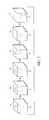
- FIGS. 8 ( a )-( c )illustrate a portion of a silicon substrate undertaking a sequence of steps for single pipe-shaped empty space formation, performed in accordance with a method of aligning a buried pattern of the present invention.
- FIGS. 9 ( a )-( b )illustrate a portion of a silicon substrate undertaking a sequence of steps for plate-shaped empty space formation, performed in accordance with a method of aligning a buried pattern of the present invention.
- FIG. 10is a cross-sectional of the silicon structure of FIG. 8, taken along line 10 - 10 ′′, at an intermediate stage of processing and in accordance with a first embodiment of the invention, and depicting the alignment mark of FIG. 5.
- FIG. 11is a cross-sectional view of the silicon structure of FIG. 10 according to the present invention at a stage of processing subsequent to that shown in FIG. 10.
- FIG. 12is a cross-sectional view of the representative silicon structure according to the present invention at a stage of processing subsequent to that shown in FIG. 11.
- FIG. 13is a cross-sectional view of the representative silicon structure according to the present invention at a stage of processing subsequent to that shown in FIG. 12.
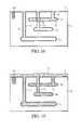
- FIG. 14is a cross-sectional view of the representative silicon structure according to a second embodiment of the present invention at a stage of processing subsequent to that shown in FIG. 12.
- FIG. 15is a cross-sectional view of the representative silicon structure according to the present invention at a stage of processing subsequent to that shown in FIG. 13.
- FIG. 16is a cross-sectional view of the representative silicon structure according to the present invention at a stage of processing subsequent to that shown in FIG. 15.
- FIG. 17is a three-dimensional view of the representative silicon structure of FIG. 16.
- FIG. 18is a cross-sectional view of the representative silicon structure according to the present invention at a stage of processing subsequent to that shown in FIG. 16.
- FIG. 19is a cross-sectional view of the representative silicon structure according to the present invention at a stage of processing subsequent to that shown in FIG. 18.
- FIG. 20is a cross-sectional view of the representative silicon structure according to the present invention at a stage of processing subsequent to that shown in FIG. 19.
- FIG. 21is a schematic diagram of a processor system incorporating a silicon structure with an alignment mark of the present invention.
- substrateused in the following description includes any semiconductor-based structure having an exposed surface in which the structure of this invention may be formed.
- substrateis to be understood as including substrates formed of silicon, silicon-on-insulator, doped and undoped semiconductors, epitaxial layers of silicon supported by a base semiconductor foundation, and other semiconductor and dielectric structures. Furthermore, when reference is made to a substrate in the following description, previous process steps may have been utilized to form regions or junctions in the base semiconductor structure or foundation.
- FIGS. 1 - 21illustrate exemplary embodiments of a method of aligning buried silicon structures 100 comprising buried conductor patterns formed in accordance with the present invention.
- FIGS. 1 - 6illustrate the formation of a series of high-temperature alignment marks 200 formed in a silicon substrate 10 according to an embodiment of the present invention.
- FIGS. 7 - 21illustrate the formation of empty-spaced patterns in the silicon substrate 10 , on which the buried conductor patterns of the present invention will be formed and aligned relative to the alignment marks 200 .
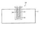
- FIG. 1illustrates a cross-sectional view of a silicon substrate 10 within which square alignment marks 200 (FIGS. 56) are formed according to exemplary embodiments of the present invention.
- square alignment marks 200FIGS. 56
- the method of the present inventionwill be described above with reference to the formation of only one square alignment mark 200 , but it must be understood the invention contemplates the formation of a plurality of such alignment marks.
- the present inventionwill be described with reference to the formation of a square alignment mark, it must be understood that the shape, geometry and configuration of the alignment mark is not limited to that of a square, and other geometries, such as crosses or chevrons, for example, may be used also.
- the silicon substrate 10is patterned and etched by known photolithography techniques to form a trench 210 in the silicon substrate 10 .
- the trench 210is etched to a depth of about 1,000 Angstroms to about 10,000 Angstroms, more preferably of about 2,000 Angstroms.
- the trench 210is also etched to a width of about one-third of the depth, or of about 300 Angstroms to about 3,000 Angstroms, in the example given.
- the silicon substrate 100is oxidized to thermally grow a silicon oxide layer 220 into the trench 210 and over the surface of the silicon substrate 10 , as illustrated in FIG. 2.
- the thermal oxidation of the silicon substrate 10could take place, for example, in an oxygen (O 2 ) or water (H 2 O) vapor ambient, at temperatures of about 750° C. to about 1000° C. depending on the desired oxidation rate.
- the silicon oxide layer 220is formed to a thickness of about 100 Angstroms to about 500 Angstroms, more preferably of about 250 Angstroms.
- the silicon oxide layer 220acts as a barrier layer to slow down the diffusion of metal atoms from a subsequently deposited metal film, the formation of which will be described in more detail below. In addition, the silicon oxide layer 220 also enhances the adherence of the metal film to the silicon substrate 10 .
- a high-temperature conductive material layer 230is formed overlying the silicon oxide layer 220 and filling partially the trench 210 .
- the conductive material layer 230is formed to a thickness of about 50 Angstroms to about 500 Angstroms, more preferably of about 100 Angstroms.
- the thickness of the conductive material layer 230determines the dimensions of alignment edge D (FIGS. 5 - 6 ). For example, if an alignment edge of about 100 Angstroms is desired, then the thickness of the conductive material layer 230 is about 100 Angstroms.
- the conductive material layer 230may be blanket deposited by a known PVD, CVD, or a combination of these techniques. Alternatively, the conductive material layer 230 may be deposited by a plating technique or by using plasma or reactive sputtering.
- the conductive material layer 230is formed of a conductive metal with a high-temperature melting point.
- a characteristic of the conductive material layer 230is that it must sustain temperatures higher than 1100° C., which are necessary for the formation of the buried structures 100 (FIG. 20) described in more detail below.
- metalssuch as iridium (Ir) or tungsten (W), which have high-temperature melting points (melting point of Ir is about 2410° C. and that of W about 3410° C. ⁇ 20° C.), are best candidates for the conductive material layer 230 .
- the preferred material for the conductive material layer 230is iridium, for example, the diffusion of iridium atoms from the iridium layer 230 is prevented by the oxide layer 220 which acts as a barrier layer as well as an adhesion layer.
- iridium and tungstenare preferred, other metals or combinations of such metals may be used also, as long as they retain a melting temperature higher than 1100° C.
- molybdenum (Mo)melting point of about 2617° C.
- tantalum (Ta)melting point of about 2996° C.
- platinum (Pt)melting point of about 1772° C.
- chromium (Cr)melting point of about 1857° C.
- Ninickel
- the term “high-temperature resistant alignment mark” as it will be used in this applicationrefers to an alignment mark which includes at least a conductive material with a melting temperature higher than an annealing temperature used to formed empty-spaced buried patterns in the substrate material by methods described in more detail below.
- a high temperature resistant alignment mark formed by a method of the present inventionincludes a conductive material capable of remaining intact at temperatures higher than about 1100° C., which, as it will be explained below, is the annealing temperature for forming empty-spaced patterns in a monocrystalline silicon substrate.
- Such annealing temperatureis, in turn, lower than the melting point of monocrystalline silicon, which is about 1400° C.
- the insulating layer 240may be formed by conventional deposition methods to a thickness of about 100 Angstroms to about 1,500 Angstroms, more preferably of about 300 Angstroms.
- portions of the oxide layer 220 , the conductive material layer 230 , and the insulating layer 240 that are formed overlying the silicon substrate 10are etched back by means of chemical mechanical polishing (CMP) or well-known RIE dry etching processes.
- CMPchemical mechanical polishing
- RIERIE dry etching processes.
- chemical mechanical polishingis employed, so that an abrasive polish removes the top surface of the insulating layer 240 as well as the horizontal portions of the oxide layer 220 and the conductive material layer 230 down to or near the planar surface of the surface of the silicon substrate 10 , as illustrated in FIG. 5.
- a high-temperature resistant alignment mark 200is formed on the silicon substrate 10 with an alignment edge D having a width determined by the thickness of the conductive material layer 230 .
- a top view of the square alignment mark 200is illustrated in FIG. 6.
- FIGS. 10 - 20illustrate exemplary embodiments of buried silicon structures 100 comprising buried conductor patterns formed within the silicon substrate 10 and aligned relative to the square alignment mark 200 (FIGS. 5 - 6 ).
- FIGS. 7 - 10wich illustrate the formation of empty-space patterns on which the buried conductor patterns of the present invention will be formed and aligned.
- Empty spaces which are formed in silicon substrates and have various shapes, such as plates, spheres or pipes,may be formed as a result of the self-organizing migration properties on the silicon surface.
- the silicon atoms on the surfacemigrate so that their surface energy is minimized.
- Sato et al.have demonstrated that the geometry of empty spaces, such as spheres, plates and pipes, formed under the surface of a silicon substrate depends on the size, number and spacing of a plurality of cylindrical holes that are initially formed at a low temperature.
- FIGS. 7 ( a )-( f )illustrate how a single sphere-shaped empty space 13 is formed from a single cylindrical hole 12 formed within the silicon substrate 10 .
- the silicon substrate 10is annealed at a temperature lower than the melting point of monocrystalline silicon (1400° C.), for example, at a temperature of about 1100° C. Sato et al. have demonstrated that, within about 60 seconds and under a reducing ambient of 10 Torr of hydrogen, the shape and surface morphology of the cylindrical hole 12 changes drastically to that of the sphere-shaped empty space 13 (FIG. 7( f )).
- the cylindrical hole 12is unstable beyond a critical length Lc and transforms, therefore, to a lower energy state consisting of one or more empty spheres formed along the original cylinder axis.
- Nnumber of empty spheres
- Rccylinder radius
- FIGS. 8 ( a )-( c )which exemplify the formation of a single pipe-shaped empty space 23 from a linear array of cylindrical holes 22 .
- FIGS. 9 ( a )-( b )illustrate the formation of a single plate-shaped empty space 33 from a two-dimensional array of cylindrical holes 32 formed within a silicon substrate such as the silicon substrate 10 .
- the values of the pipe radius Rp (of the pipe-shaped empty space 23 ) and that of the plate thickness Tp (of the plate-shaped empty space 33 )may be calculated in a manner similar to that described above with reference to the formation of the empty sphere 13 and the calculation of sphere radius Rs in equation (2).
- the distance A between the centers of any two adjacent cylindrical holes 22 , 32 , in a linear arraymay be calculated from the following formula:
- ⁇center-to-center distance between two adjacent cylinder holes in a linear array
- Equation (4)ensures that adjacent cylindrical holes 22 , 32 do not touch each other allowing, therefore, the formation of a plurality of adjacent spheres that combine to form the resulting pipe-shaped empty space 23 and plate-shaped empty space 33 .
- Rppipe radius
- Tpplate thickness
- ⁇center-to-center distance between two adjacent cylinder holes in a linear array
- FIG. 10illustrates a cross-sectional view of structure of FIG. 8( a ) on which a plurality of linear cylindrical holes 22 are drilled into silicon substrate 10 which also includes high-temperature alignment marks, such as the alignment mark 200 (FIGS. 5 - 6 ), the formation of which was described above.
- the linear cylindrical holes 22are drilled into silicon substrate 10 from an upper surface 11 of the substrate 10 to a depth D 1 .
- the silicon substrate 10is annealed at a temperature of about 1100° C. and under a reducing ambient of about 10 Torr of hydrogen so that within about 60 seconds a pipe-shaped empty space 23 is formed within the silicon substrate 10 as shown in FIG. 11.
- Radius R 1 (FIG. 10) of each of the cylindrical holes 22 and distance ⁇ 1 (FIG. 10) between the center of two adjacent cylindrical holes 22may be calculated in accordance with equation (4). It must be understood that the length L 1 (FIG. 10) of the array of the cylindrical holes 22 determines the length L 1 (FIG. 11) of the pipe-shaped empty space 23 , wherein the depth D 1 (FIG. 10) to which the array of cylindrical holes 22 is drilled determines the depth DI (FIG. 11) at which the pipe-shaped empty space 23 is formed. Both parameters define a location where a first level conductor 70 (FIGS. 19 - 20 ), will be formed as described in more detail below. Finally, the radius Rp of the pipe-shaped empty space 23 (FIG. 11) may be calculated in accordance with equation (5).
- a second pipe-shaped empty space 43(FIG. 13) may be formed above the pipe-shaped empty space 23 and below the silicon surface 11 by a technique similar to that described for the formation of the pipe-shaped empty space 23 (FIG. 11).
- a second linear array of cylindrical holes 42(FIG. 12) are drilled into the silicon substrate 10 to a depth D 2 to define the intended location, length and orientation of a second level conductor 80 (FIGS. 19 - 20 ), the formation of which will be described in more detail below.
- the relative positioning between the pipe-shaped empty space 23 (FIG. 11) and the second linear array of cylindrical holes 42 (FIG. 12)is accomplished by reference to the alignment mark 200 . This way, the second linear array of cylindrical holes 42 is accurately aligned to the already formed pipe-shaped empty space 23 .
- the silicon substrate 10is then annealed at a temperature of about 1100° C. and under a reducing ambient of about 10 Torr of hydrogen, so that within about 60 seconds the second linear array of cylindrical holes 42 transforms into the second pipe-shaped empty space 43 (FIG. 13) by steps similar to those described above with reference to FIGS. 8 ( a )-( c ).
- Radius R 2 (FIG. 12) as well as distance ⁇ 2 (FIG. 12) between the center of two adjacent cylindrical holes 42 of the second linear arraymay be calculated in accordance to equation (4). Further, the length L 2 (FIG. 12) of the second linear array of cylindrical holes determines the length L 2 (FIG. 13) of the second pipe-shaped empty space 43 , wherein the depth D 2 (FIG. 12) to which the second linear array of cylindrical holes is drilled determines the depth D 2 (FIG. 13) at which the second pipe-shaped empty space 43 is formed within the silicon substrate 10 .
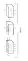
- FIG. 13illustrates the second pipe-shaped empty space 43 as being parallel to the pipe-shaped empty space 23
- the second pipe-shaped empty space 43need not be parallel to the pipe-shaped empty space 23 but may form various angles and may be placed in various directions with respect to the pipe-shaped empty space 23 , according to the characteristics of the IC device to be formed.
- FIG. 14illustrates the second pipe-shaped empty space 43 forming a 90 degree angle with the pipe-shaped empty space 23 .
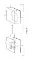
- FIG. 15illustrates the formation of a two-dimensional array of cylindrical holes 52 located in between the upper silicon surface 11 and the second pipe-shaped empty space 43 which will form a plate-shaped empty space 53 (FIG. 16) aligned relative to the alignment mark 200 .
- the silicon substrate 10is annealed at a temperature of about 1100° C. and under a reducing ambient of about 10 Torr of hydrogen, so that within about 60 seconds the two-dimensional array of cylindrical holes 52 transforms into the plate-shaped empty space 53 (FIG. 16) by steps similar to those described above with reference to FIGS. 9 ( a )-( b ).
- FIG. 16the structures of FIG. 16 are illustrated in a three-dimensional view in FIG. 17.
- Radius R 3 (FIG. 15) as well as distance ⁇ 3 (FIG. 15) between the center of two adjacent cylindrical holes 52 of the two-dimensional arraymay be calculated in accordance to equation (4). Further, the length L 3 (FIG. 15) of the two-dimensional array of cylindrical holes determines the length L 3 (FIG. 16) of the plate-shaped empty space 53 , wherein the depth D 3 (FIG. 15) to which the two-dimensional array of cylindrical holes is drilled determines the depth D 3 (FIGS. 16 - 17 ) at which the plate-shaped empty space 53 is formed within the silicon substrate 10 . Finally, the thickness Tp (FIGS. 16 - 17 ) of the plate-shaped empty space 53 may be calculated in accordance with equation (6).
- This plate-shaped empty regionmay be left empty in some areas, so that the region above the plate becomes a silicon-over-nothing area where various IC devices can then be formed.
- the plate-shaped empty regionmay be also filled with a conductor, as it will be described in more detail below, to provide a plate-shaped conductor region.
- additional interconnect structures and associated dielectric layerscould be formed to create operative electrical paths down from the empty-spaced structures formed within the silicon substrate 10 and up to the silicon surfaces, such as the upper silicon surface 11 , and any IC devices formed thereon.
- These additional interconnect structures and associated dielectric layersare also aligned with the previous empty space structures 23 , 43 , 53 by reference to the alignment mark 200 .
- the aligning method of the present inventionis further explained below with reference to the formation and alignment of buried conductor patterns 70 , 80 , 90 (FIG. 20) relative to the alignment mark 200 .
- a plurality of interconnect holes 25 , 45 , 55are drilled within the silicon substrate 10 to connect each of the first pipe-shaped empty space 23 , the second pipe-shaped empty space 43 , and the plate-shaped empty space 53 with the upper silicon surface 11 .
- a conventional oxidizing atmospherefor example an ozone oxidizing atmosphere or water vapor is heated and passed over the substrate at about 600-700° C., so that the inner surfaces of the above-described patterns, as well as the interconnect holes 24 , 45 , 55 , are oxidized to prevent any leakage between conductors formed in areas 23 , 43 , 53 , the substrate and any active devices that will be eventually fabricated over the silicon substrate 10 .
- a conventional oxidizing atmospherefor example an ozone oxidizing atmosphere or water vapor is heated and passed over the substrate at about 600-700° C.
- a barrier layer 72may be formed on surfaces of the silicon substrate 10 , within each of the interconnect holes 24 , 45 , 55 , and on the inner surfaces of each of the first pipe-shaped empty space 23 , the second pipe-shaped empty space 43 , and the plate-shaped empty space 53 , as also shown in FIG. 18.
- the barrier layer 72may be formed by CVD, PVD, sputtering or evaporation, to a thickness of about 50 Angstroms to about 100 Angstroms.
- Preferred materials for the barrier layer 72are metals, such as titanium (Ti), zirconium (Zr), tungsten (W), or hafnium (Hf), or metal compounds, such as tantalum nitride (TaN) or silicon nitride (Si 3 N 4 ).
- the barrier layer 72may be formed of refractory metal compounds, such as refractory metal nitrides (for example TiN and HfN), refractory metal carbides (for example TiC or WC), or refractory metal borides (for example TiB or MoB). The selection of a material for the barrier layer 72 depends upon the specific conductor to be deposited and the method which is chosen to deposit such conductor.
- the selection of the conductor materialwill depend upon the type and temperature of subsequent processing steps. For example, aluminum (Al) would not be chosen as the conductor material if the subsequent processing steps require temperatures above approximately 600° C. Similarly, tungsten (W) would be a preferred conductor for temperatures above approximately 1000° C.
- the barrier layer 72suppresses the diffusion of the metal atoms from the subsequently deposited conductive material (FIG. 20), while offering a low resistivity and low contact resistance between the subsequently deposited conductive material (FIG. 20) and the barrier layer 72 .
- the barrier layer 72is simultaneously deposited in the interconnect holes 24 , 45 , 55 , and on the inner surfaces of each of the first pipe-shaped empty space 23 , the second pipe-shaped empty space 43 , and the plate-shaped empty space 53 , the invention is not limited to this embodiment.
- the barrier layer 72may be deposited first in the interconnect hole 24 and its corresponding pipe-shaped empty space 23 , before the formation of the interconnect hole 45 and its corresponding second pipe-shaped empty space 43 , and before the formation of the interconnect hole 55 and its corresponding plate-shaped empty space 53 .
- the barrier layer 72may be formed of a first barrier material corresponding to the pipe-shaped empty space 23 , of a second barrier material corresponding to the second pipe-shaped empty space 43 , and of a third barrier material corresponding to the plate-shaped empty space 53 .
- the first, second and third barrier materialsmay be the same or different, depending on the characteristics of the IC device.
- a conductive material 73is next deposited to fill in the interconnect holes 24 , 45 , 55 , as well as the first pipe-shaped empty space 23 , the second pipe-shaped empty space 43 , and the plate-shaped empty space 53 .
- the conductive material 73comprises either copper, silver, gold, tungsten or aluminum, but it must be understood that other conductive materials and/or their alloys may be used also.
- the conductive material 73may be blanket deposited by a substitution technique, as described in U.S. Pat. Nos. 5,920,121; 6,100,176; 6,121,126, and U.S. application Ser. No. 09/069,346 filed Apr.
- the conductive material 73may be also blanket deposited by a known PVD, CVD, or a combination of these techniques to fill in all three interconnect holes 24 , 45 , 55 and their associated first pipe-shaped empty space 23 , second pipe-shaped empty space 43 , and plate-shaped empty space 53 to form a first buried conductor pattern 70 , a second buried conductor pattern 80 , and a third buried conductor pattern 90 , all illustrated in FIG. 20.
- the conductive material 73may be deposited by a plating technique.
- CMPchemical mechanical polishing
- the buried silicon structure 100is shown in FIG. 20 as comprising only three buried conductor patterns 70 , 80 , and 90 , respectively, it must be readily apparent to those skilled in the art that in fact any number of such buried conductor patterns may be formed on the substrate 10 , as pipes, plates, or spheres and aligned relative to the alignment mark 200 , by methods of the present invention.
- the exemplary embodiments described aboverefer to the formation of buried conductor patterns having specific shapes, it must be understood that other shapes, configurations or geometries may be employed, depending on the characteristics of the particular IC device to be fabricated and as long as they are accurately aligned with the previously formed patterns.
- the inventionis not limited to a combination of three buried conductor patterns, but any combination of any number of empty-spaced patterns filled with a conductor may be employed, as desired.
- the processing steps of the present inventionmay be also reduced if the lower level buried conductor patterns do not cross over each other below upper level buried patterns, such as the plate-shaped empty space 53 (FIGS. 16 - 18 ). In this case, all buried conductor patterns located below the plate-shaped empty space 53 may be simultaneously aligned and formed during the same annealing/heating cycle, to reduce therefore the number of processing steps during the fabrication of the buried silicon structure 100 .
- additional multilevel interconnect layers and associated dielectric layerscould be formed to create operative electrical paths from the buried silicon structure 100 to a source/drain region (not shown) adjacent to a transistor gate structure (not shown) of the substrate 10 .
- These additional multilevel interconnect layers and associated dielectric layersmay be also positioned and aligned with the buried conductor patterns 70 , 80 , 90 (FIG. 20) with reference to the mark 200 , to minimize misalignment between the IC layers.
- the resulting substrate containing the buried conductorscan be used in the formation of many types of integrated circuits such as memories, for example, DRAMs, processors etc.
- the inventionprovides a technique for forming buried conductors in semiconductor substrates which are aligned relative to an high-temperature alignment mark and may be further used, for example, as interconnects to various structures and devices in an integrated circuit.
- a typical processor-based system 400which includes a memory circuit 448 , for example a DRAM, is illustrated in FIG. 21.
- a processor systemsuch as a computer system, generally comprises a central processing unit (CPU) 444 , such as a microprocessor, a digital signal processor, or other programmable digital logic devices, which communicates with an input/output (I/O) device 446 over a bus 452 .
- the memory 448communicates with the system over bus 452 .
- the processor systemmay include peripheral devices such as a floppy disk drive 454 and a compact disk (CD) ROM drive 456 which also communicate with CPU 444 over the bus 452 .
- Memory 448 , the CPU 444 or others of the illustrated electrical structuresmay be constructed as an integrated circuit, which includes one or more buried silicon structures 100 aligned relative to the high-temperature alignment mark 200 in accordance with the invention. If desired, the memory 448 may be combined with the processor, for example CPU 444 , in a single integrated circuit.
Landscapes
- Physics & Mathematics (AREA)
- General Physics & Mathematics (AREA)
- Engineering & Computer Science (AREA)
- Condensed Matter Physics & Semiconductors (AREA)
- Computer Hardware Design (AREA)
- Microelectronics & Electronic Packaging (AREA)
- Power Engineering (AREA)
- Manufacturing & Machinery (AREA)
- Exposure And Positioning Against Photoresist Photosensitive Materials (AREA)
Abstract
Description
- The present invention relates to semiconductor devices and methods of making such devices. More particularly, the invention relates to solid state materials and to a novel method of aligning buried structures formed in such solid state materials.[0001]
- The fabrication of integrated circuits (IC) devices on semiconductor wafers include various steps during which patterns are transferred from photolithographic masks on the wafers. The masking step involves an etching step and defines predefined areas to be exposed on the wafer for subsequent processing, for example, oxidation, metallization, or doping, among others. This photolithographic process is repetitively performed until desired patterns of materials are formed on the semiconductor wafer.[0002]
- As the dimensions of these patterns become increasingly smaller, it is strictly required to accurately align the patterns previously formed on the semiconductor wafer with a pattern that is to be subsequently formed, and to minimize the misalignment between IC layers. To accurately carry out this process, the semiconductor industry employs alignment marks which are provided at predetermined position on the surface of a wafer, so that relative positioning between patterns is performed referring to these marks.[0003]
- Typically, alignment marks are topographical patterns, such as squares, crosses or chevrons, among others, which are formed by etching into the wafer to provide slit patterns constituted of longitudinal indentations over specific intervals at semiconductor surface, an insulating layer or other layers of a semiconductor substrate.[0004]
- The formation of alignment marks is typically executed simultaneously with, or after, other processes, for example the formation of metallization layers over a semiconductor substrate. In this case, the etching of the alignment mark must be conducted with extreme care, to avoid overetching of the substrate and/or of the underlying layers, which could be metal layers. Another problem posed by the formation of the alignment marks under these circumstances is the readability of the mark, particularly when an oxide layer covers the mark. As known in the industry, the formation of semiconductor devices requires, in most cases, a series of oxidation steps to form various oxide layers at different stages of processing. For example, new isolation processes such as shallow trench isolation (STI) necessitate a thick oxide layer formed over both the wafer and the alignment marks. When the thick oxide layer is later polished, typically by chemical mechanical polishing, to create a planar surface, the alignment marks on a new overlying layer on the wafer are flattened after planarization, causing alignment target reading problems.[0005]
- Another problem encountered by conventional alignment processes relates to the alignment of various buried structures. As the semiconductor industry is exploring new ways of increasing the amount of active surface area on the integrated circuit chips, particularly on those employing monocrystalline semiconductor substrates, attempts to create and develop new technologies have been made continuously. For example, one technology proposed by the semiconductor industry is the so-called Silicon-On-Insulator (SOI) process, wherein oxygen atoms are implanted at high dose and energy to form a silicon dioxide insulating layer between the upper surface of the original monocrystalline substrate and the bottom bulk portion of the same substrate. Although the SOI devices have many advantages, such as reduced parasitic capacitance due to the buried insulating layer, the process is relatively expensive because of the high costs of implanting the oxygen atoms and curing of the implant-induced defects. Further, buried structures such as SOI devices are completely covered by the reformed monocrystalline semiconductor substrate and thus they become essentially non-readable for alignment purposes.[0006]
- Accordingly, there is a need for an improved method of increasing the available active surface area on integrated circuit chips fabricated on monocrystalline substrates by forming buried structures within such substrates. There is also a need for a more advantageous alignment process for such buried structures formed in monocrystalline superconducting substrates. There is further a need for an improved metallization scheme which facilitates the formation of active devices on SOI substrates and on the more novel Silicon-On-Nothing (SON) substrates, as well as a need for accurate alignment of such metallization scheme with subsequently formed layers.[0007]
- The present invention provides a method of forming an alignment mark for aligning a plurality of empty-spaced patterns formed in semiconductor monocrystalline substrates. According to an exemplary embodiment, alignment metal marks are formed of a conductive material having a melting temperature higher than the annealing temperature used to form the empty-spaced patterns. The alignment marks are formed prior to the formation of empty-spaced buried patterns formed in a monocrystalline substrate, so that the empty-space buried patterns are aligned to the marks. Holes could be next formed in the monocrystalline substrate to connect surfaces of the substrate with the previously formed empty-space patterns. The whole assembly is subsequently exposed to an oxidizing atmosphere so that the inner surfaces of the empty-space patterns are oxidized. The empty-space patterns could then be filled with a suitable conducting material to form, for example, buried conductors and/or buried plate patterns. Subsequent semiconductor structures that are formed as part of desired semiconductor devices can be also aligned to the marks. This way, a proper alignment of the semiconductor devices to the buried conductors and/or buried plate patterns is achieved.[0008]
- FIG. 1 illustrates a cross-sectional view of a silicon substrate at a preliminary step of processing undertaking a sequence of steps for the formation of an alignment mark in accordance with a method of the present invention.[0009]
- FIG. 2 illustrates a cross-sectional view of the alignment mark of FIG. 1 at a stage of processing subsequent to that shown in FIG. 1.[0010]
- FIG. 3 illustrates a cross-sectional view of the alignment mark of FIG. 1 at a stage of processing subsequent to that shown in FIG. 2.[0011]
- FIG. 4 illustrates a cross-sectional view of the alignment mark of FIG. 1 at a stage of processing subsequent to that shown in FIG. 3.[0012]
- FIG. 5 illustrates a cross-sectional view of the alignment mark of FIG. 1 at a stage of processing subsequent to that shown in FIG. 4.[0013]
- FIG. 6 illustrates a top view of the alignment mark of FIG. 1 at a stage of processing subsequent to that shown in FIG. 5.[0014]
- FIGS.[0015]7(a)-(f) illustrate a portion of a silicon substrate undertaking a sequence of steps for single-shaped sphere formation.
- FIGS.[0016]8(a)-(c) illustrate a portion of a silicon substrate undertaking a sequence of steps for single pipe-shaped empty space formation, performed in accordance with a method of aligning a buried pattern of the present invention.
- FIGS.[0017]9(a)-(b) illustrate a portion of a silicon substrate undertaking a sequence of steps for plate-shaped empty space formation, performed in accordance with a method of aligning a buried pattern of the present invention.
- FIG. 10 is a cross-sectional of the silicon structure of FIG. 8, taken along line[0018]10-10″, at an intermediate stage of processing and in accordance with a first embodiment of the invention, and depicting the alignment mark of FIG. 5.
- FIG. 11 is a cross-sectional view of the silicon structure of FIG. 10 according to the present invention at a stage of processing subsequent to that shown in FIG. 10.[0019]
- FIG. 12 is a cross-sectional view of the representative silicon structure according to the present invention at a stage of processing subsequent to that shown in FIG. 11.[0020]
- FIG. 13 is a cross-sectional view of the representative silicon structure according to the present invention at a stage of processing subsequent to that shown in FIG. 12.[0021]
- FIG. 14 is a cross-sectional view of the representative silicon structure according to a second embodiment of the present invention at a stage of processing subsequent to that shown in FIG. 12.[0022]
- FIG. 15 is a cross-sectional view of the representative silicon structure according to the present invention at a stage of processing subsequent to that shown in FIG. 13.[0023]
- FIG. 16 is a cross-sectional view of the representative silicon structure according to the present invention at a stage of processing subsequent to that shown in FIG. 15.[0024]
- FIG. 17 is a three-dimensional view of the representative silicon structure of FIG. 16.[0025]
- FIG. 18 is a cross-sectional view of the representative silicon structure according to the present invention at a stage of processing subsequent to that shown in FIG. 16.[0026]
- FIG. 19 is a cross-sectional view of the representative silicon structure according to the present invention at a stage of processing subsequent to that shown in FIG. 18.[0027]
- FIG. 20 is a cross-sectional view of the representative silicon structure according to the present invention at a stage of processing subsequent to that shown in FIG. 19.[0028]
- FIG. 21 is a schematic diagram of a processor system incorporating a silicon structure with an alignment mark of the present invention.[0029]
- DETAILED DESCRIPTION OF THE IVNTION[0030]
- In the following detailed description, reference is made to various exemplary embodiments for carrying out the invention. These embodiments are described with sufficient detail to enable those skilled in the art to practice the invention, and it is to be understood that other embodiments may be employed, and that structural, electrical and process changes may be made, and equivalents substituted, without departing from the invention. Accordingly, the following detailed description is exemplary and the scope of the present invention is defined by the appended claims.[0031]
- The term “substrate” used in the following description includes any semiconductor-based structure having an exposed surface in which the structure of this invention may be formed. The term “substrate” is to be understood as including substrates formed of silicon, silicon-on-insulator, doped and undoped semiconductors, epitaxial layers of silicon supported by a base semiconductor foundation, and other semiconductor and dielectric structures. Furthermore, when reference is made to a substrate in the following description, previous process steps may have been utilized to form regions or junctions in the base semiconductor structure or foundation.[0032]
- The following illustration is for a particular embodiment in a silicon structure. However, it should be apparent to one skilled in the art that a similar embodiment is possible in any semiconductor structure.[0033]
- Referring now to the drawings, where like elements are designated by like reference numerals, FIGS.[0034]1-21 illustrate exemplary embodiments of a method of aligning buried
silicon structures 100 comprising buried conductor patterns formed in accordance with the present invention. FIGS.1-6 illustrate the formation of a series of high-temperature alignment marks200 formed in asilicon substrate 10 according to an embodiment of the present invention. FIGS.7-21 illustrate the formation of empty-spaced patterns in thesilicon substrate 10, on which the buried conductor patterns of the present invention will be formed and aligned relative to the alignment marks200. - Reference in now made to FIG. 1, which illustrates a cross-sectional view of a[0035]
silicon substrate 10 within which square alignment marks200 (FIGS. 56) are formed according to exemplary embodiments of the present invention. For simplicity, the method of the present invention will be described above with reference to the formation of only onesquare alignment mark 200, but it must be understood the invention contemplates the formation of a plurality of such alignment marks. Further, although the present invention will be described with reference to the formation of a square alignment mark, it must be understood that the shape, geometry and configuration of the alignment mark is not limited to that of a square, and other geometries, such as crosses or chevrons, for example, may be used also. - As shown in FIG. 1, the[0036]
silicon substrate 10 is patterned and etched by known photolithography techniques to form atrench 210 in thesilicon substrate 10. Thetrench 210 is etched to a depth of about 1,000 Angstroms to about 10,000 Angstroms, more preferably of about 2,000 Angstroms. Thetrench 210 is also etched to a width of about one-third of the depth, or of about 300 Angstroms to about 3,000 Angstroms, in the example given. - Subsequent to the formation of the[0037]
trench 210, thesilicon substrate 100 is oxidized to thermally grow asilicon oxide layer 220 into thetrench 210 and over the surface of thesilicon substrate 10, as illustrated in FIG. 2. The thermal oxidation of thesilicon substrate 10 could take place, for example, in an oxygen (O2) or water (H2O) vapor ambient, at temperatures of about 750° C. to about 1000° C. depending on the desired oxidation rate. This way, thesilicon oxide layer 220 is formed to a thickness of about 100 Angstroms to about 500 Angstroms, more preferably of about 250 Angstroms. Thesilicon oxide layer 220 acts as a barrier layer to slow down the diffusion of metal atoms from a subsequently deposited metal film, the formation of which will be described in more detail below. In addition, thesilicon oxide layer 220 also enhances the adherence of the metal film to thesilicon substrate 10. - Next, as illustrated in FIG. 3, a high-temperature[0038]
conductive material layer 230 is formed overlying thesilicon oxide layer 220 and filling partially thetrench 210. Theconductive material layer 230 is formed to a thickness of about 50 Angstroms to about 500 Angstroms, more preferably of about 100 Angstroms. The thickness of theconductive material layer 230 determines the dimensions of alignment edge D (FIGS.5-6). For example, if an alignment edge of about 100 Angstroms is desired, then the thickness of theconductive material layer 230 is about 100 Angstroms. In any event, theconductive material layer 230 may be blanket deposited by a known PVD, CVD, or a combination of these techniques. Alternatively, theconductive material layer 230 may be deposited by a plating technique or by using plasma or reactive sputtering. - In a preferred embodiment of the invention, the[0039]
conductive material layer 230 is formed of a conductive metal with a high-temperature melting point. A characteristic of theconductive material layer 230 is that it must sustain temperatures higher than 1100° C., which are necessary for the formation of the buried structures100 (FIG. 20) described in more detail below. For example, metals such as iridium (Ir) or tungsten (W), which have high-temperature melting points (melting point of Ir is about 2410° C. and that of W about 3410° C.±20° C.), are best candidates for theconductive material layer 230. If the preferred material for theconductive material layer 230 is iridium, for example, the diffusion of iridium atoms from theiridium layer 230 is prevented by theoxide layer 220 which acts as a barrier layer as well as an adhesion layer. - Although iridium and tungsten are preferred, other metals or combinations of such metals may be used also, as long as they retain a melting temperature higher than 1100° C. As such, molybdenum (Mo) (melting point of about 2617° C.), tantalum (Ta) (melting point of about 2996° C.), platinum (Pt) (melting point of about 1772° C.), chromium (Cr) (melting point of about 1857° C.), nickel (Ni) (melting point of about 1453° C.), or combinations of these metals may be used also. In any event, the term “high-temperature resistant alignment mark” as it will be used in this application refers to an alignment mark which includes at least a conductive material with a melting temperature higher than an annealing temperature used to formed empty-spaced buried patterns in the substrate material by methods described in more detail below. Thus, for a monocrystalline silicon substrate, such as the[0040]
silicon substrate 10 of the present invention, a high temperature resistant alignment mark formed by a method of the present invention includes a conductive material capable of remaining intact at temperatures higher than about 1100° C., which, as it will be explained below, is the annealing temperature for forming empty-spaced patterns in a monocrystalline silicon substrate. Such annealing temperature is, in turn, lower than the melting point of monocrystalline silicon, which is about 1400° C. - Referring now to FIG. 4, an insulating[0041]
layer 240 of, for example, silicon nitride (Si3N4) or an oxide such as silicon dioxide (SiO2), is formed overlying theconductive material layer 230 and filling completely thetrench 210. The insulatinglayer 240 may be formed by conventional deposition methods to a thickness of about 100 Angstroms to about 1,500 Angstroms, more preferably of about 300 Angstroms. - Subsequent to the formation of the insulating[0042]
layer 240, portions of theoxide layer 220, theconductive material layer 230, and the insulatinglayer 240 that are formed overlying thesilicon substrate 10 are etched back by means of chemical mechanical polishing (CMP) or well-known RIE dry etching processes. In a preferred embodiment, chemical mechanical polishing is employed, so that an abrasive polish removes the top surface of the insulatinglayer 240 as well as the horizontal portions of theoxide layer 220 and theconductive material layer 230 down to or near the planar surface of the surface of thesilicon substrate 10, as illustrated in FIG. 5. This way, a high-temperatureresistant alignment mark 200 is formed on thesilicon substrate 10 with an alignment edge D having a width determined by the thickness of theconductive material layer 230. For a better understanding, a top view of thesquare alignment mark 200 is illustrated in FIG. 6. - Reference is now made to FIGS.[0043]10-20, which illustrate exemplary embodiments of buried
silicon structures 100 comprising buried conductor patterns formed within thesilicon substrate 10 and aligned relative to the square alignment mark200 (FIGS.5-6). To understand, however, the formation of such buried conductor patterns, reference is first made to FIGS.7-10 wich illustrate the formation of empty-space patterns on which the buried conductor patterns of the present invention will be formed and aligned. Techniques for the formation of empty-spaced patterns of different geometries are described by Sato et al., inSubstrate Engineering for the Formation of Empty Space in Silicon(ESS)Induced by Silicon Surface Migration,1999 IEDM Digest, Paper 20.6.1, the disclosure of which is incorporated by reference herein. - Empty spaces which are formed in silicon substrates and have various shapes, such as plates, spheres or pipes, may be formed as a result of the self-organizing migration properties on the silicon surface. As such, when deeply-etched silicon substrates are annealed in a hydrogen ambient, for example, the silicon atoms on the surface migrate so that their surface energy is minimized. Based on these findings, Sato et al. have demonstrated that the geometry of empty spaces, such as spheres, plates and pipes, formed under the surface of a silicon substrate depends on the size, number and spacing of a plurality of cylindrical holes that are initially formed at a low temperature.[0044]
- For example, FIGS.[0045]7(a)-(f) illustrate how a single sphere-shaped
empty space 13 is formed from a single cylindrical hole12 formed within thesilicon substrate 10. Subsequent to the formation of the cylindrical hole12, thesilicon substrate 10 is annealed at a temperature lower than the melting point of monocrystalline silicon (1400° C.), for example, at a temperature of about 1100° C. Sato et al. have demonstrated that, within about 60 seconds and under a reducing ambient of 10 Torr of hydrogen, the shape and surface morphology of the cylindrical hole12 changes drastically to that of the sphere-shaped empty space13 (FIG. 7(f)). Because of the significant surface and/or volume diffusion which occurs at high annealing temperatures, the cylindrical hole12 is unstable beyond a critical length Lc and transforms, therefore, to a lower energy state consisting of one or more empty spheres formed along the original cylinder axis. - As analyzed by Nichols et al., in[0046]Surface—(Interface—)and Volume—Diffusion Contributions to Morphological Changes Driven by Capillarity, Trans. AIME 233 at 1840 (October 1965), the disclosure of which is incorporated by reference herein, when Lc corresponds to the surface diffusion state, the number N of empty spheres that form from a cylindrical hole depends both on the length L of the cylindrical hole and on the cylinder radius Rc. Accordingly, the number N of empty spheres formed from a cylindrical hole made in a silicon substrate could be estimated according to the following equation:
- 8.89RcN<L<8.89Rc(N+1) (1)
- wherein: N=number of empty spheres;[0047]
- Rc=cylinder radius; and[0048]
- L=length of cylindrical hole[0049]
- Thus, equation (1) predicts that, if L<8.89 Rc, the number of empty spheres will be N=0, which means that no empty spheres will form from a cylindrical hole.[0050]
- When one or more empty spheres form with a radius Rs, then according to Nichols et al., the value of Rs is given by the following equation:[0051]
- Rs=1.88Rc (2)
- wherein: Rs=sphere radius; and[0052]
- Rc=cylinder radius[0053]
- When two or more empty spheres form from a cylinder hole with a cylinder radius Rc, then the distance X between the centers of two adjacent empty-spaced spheres is calculated from the following formula:[0054]
- λ=8.89Rc (3)
- wherein: λ=center-to-center distance between two adjacent spheres; and[0055]
- Rc=cylinder radius[0056]
- Reference is now made to FIGS.[0057]8(a)-(c), which exemplify the formation of a single pipe-shaped
empty space 23 from a linear array ofcylindrical holes 22. Similarly, FIGS.9(a)-(b) illustrate the formation of a single plate-shapedempty space 33 from a two-dimensional array ofcylindrical holes 32 formed within a silicon substrate such as thesilicon substrate 10. The values of the pipe radius Rp (of the pipe-shaped empty space23) and that of the plate thickness Tp (of the plate-shaped empty space33) may be calculated in a manner similar to that described above with reference to the formation of theempty sphere 13 and the calculation of sphere radius Rs in equation (2). The distance A between the centers of any two adjacentcylindrical holes - 2Rc<Δ<3.76Rc (4)
- wherein: Rc=cylinder radius; and[0058]
- Δ=center-to-center distance between two adjacent cylinder holes in a linear array[0059]
- Equation (4) ensures that adjacent[0060]
cylindrical holes empty space 23 and plate-shapedempty space 33. - The values of the pipe radius Rp and of the plate thickness Tp are given by the following two expressions:[0061]
- Rp=(8.86Rc3/Δ)½ (5)
- Tp=27.83Rc3/Δ2 (6)
- wherein: Rp=pipe radius;[0062]
- Tp=plate thickness; and[0063]
- Δ=center-to-center distance between two adjacent cylinder holes in a linear array[0064]
- Reference is now made to FIG. 10 which, for simplicity, illustrates a cross-sectional view of structure of FIG. 8([0065]a) on which a plurality of linear
cylindrical holes 22 are drilled intosilicon substrate 10 which also includes high-temperature alignment marks, such as the alignment mark200 (FIGS.5-6), the formation of which was described above. The linearcylindrical holes 22 are drilled intosilicon substrate 10 from anupper surface 11 of thesubstrate 10 to a depth D1. Thesilicon substrate 10 is annealed at a temperature of about 1100° C. and under a reducing ambient of about 10 Torr of hydrogen so that within about 60 seconds a pipe-shapedempty space 23 is formed within thesilicon substrate 10 as shown in FIG. 11. - Radius R[0066]1 (FIG. 10) of each of the
cylindrical holes 22 and distance Δ1 (FIG. 10) between the center of two adjacentcylindrical holes 22 may be calculated in accordance with equation (4). It must be understood that the length L1 (FIG. 10) of the array of thecylindrical holes 22 determines the length L1 (FIG. 11) of the pipe-shapedempty space 23, wherein the depth D1 (FIG. 10) to which the array ofcylindrical holes 22 is drilled determines the depth DI (FIG. 11) at which the pipe-shapedempty space 23 is formed. Both parameters define a location where a first level conductor70 (FIGS.19-20), will be formed as described in more detail below. Finally, the radius Rp of the pipe-shaped empty space23 (FIG. 11) may be calculated in accordance with equation (5). - Subsequent to the formation of the pipe-shaped[0067]
empty space 23, a second pipe-shaped empty space43 (FIG. 13) may be formed above the pipe-shapedempty space 23 and below thesilicon surface 11 by a technique similar to that described for the formation of the pipe-shaped empty space23 (FIG. 11). As such, a second linear array of cylindrical holes42 (FIG. 12) are drilled into thesilicon substrate 10 to a depth D2 to define the intended location, length and orientation of a second level conductor80 (FIGS.19-20), the formation of which will be described in more detail below. The relative positioning between the pipe-shaped empty space23 (FIG. 11) and the second linear array of cylindrical holes42 (FIG. 12) is accomplished by reference to thealignment mark 200. This way, the second linear array ofcylindrical holes 42 is accurately aligned to the already formed pipe-shapedempty space 23. - The[0068]
silicon substrate 10 is then annealed at a temperature of about 1100° C. and under a reducing ambient of about 10 Torr of hydrogen, so that within about 60 seconds the second linear array ofcylindrical holes 42 transforms into the second pipe-shaped empty space43 (FIG. 13) by steps similar to those described above with reference to FIGS.8(a)-(c). - Radius R[0069]2 (FIG. 12) as well as distance Δ2 (FIG. 12) between the center of two adjacent
cylindrical holes 42 of the second linear array may be calculated in accordance to equation (4). Further, the length L2 (FIG. 12) of the second linear array of cylindrical holes determines the length L2 (FIG. 13) of the second pipe-shapedempty space 43, wherein the depth D2 (FIG. 12) to which the second linear array of cylindrical holes is drilled determines the depth D2 (FIG. 13) at which the second pipe-shapedempty space 43 is formed within thesilicon substrate 10. - Although FIG. 13 illustrates the second pipe-shaped[0070]
empty space 43 as being parallel to the pipe-shapedempty space 23, it must be understood that the second pipe-shapedempty space 43 need not be parallel to the pipe-shapedempty space 23 but may form various angles and may be placed in various directions with respect to the pipe-shapedempty space 23, according to the characteristics of the IC device to be formed. For example, FIG. 14 illustrates the second pipe-shapedempty space 43 forming a 90 degree angle with the pipe-shapedempty space 23. - FIG. 15 illustrates the formation of a two-dimensional array of[0071]
cylindrical holes 52 located in between theupper silicon surface 11 and the second pipe-shapedempty space 43 which will form a plate-shaped empty space53 (FIG. 16) aligned relative to thealignment mark 200. Again, thesilicon substrate 10 is annealed at a temperature of about 1100° C. and under a reducing ambient of about 10 Torr of hydrogen, so that within about 60 seconds the two-dimensional array ofcylindrical holes 52 transforms into the plate-shaped empty space53 (FIG. 16) by steps similar to those described above with reference to FIGS.9(a)-(b). For a better understanding of the invention, the structures of FIG. 16 are illustrated in a three-dimensional view in FIG. 17. - Radius R[0072]3 (FIG. 15) as well as distance Δ3 (FIG. 15) between the center of two adjacent
cylindrical holes 52 of the two-dimensional array may be calculated in accordance to equation (4). Further, the length L3 (FIG. 15) of the two-dimensional array of cylindrical holes determines the length L3 (FIG. 16) of the plate-shapedempty space 53, wherein the depth D3 (FIG. 15) to which the two-dimensional array of cylindrical holes is drilled determines the depth D3 (FIGS.16-17) at which the plate-shapedempty space 53 is formed within thesilicon substrate 10. Finally, the thickness Tp (FIGS.16-17) of the plate-shapedempty space 53 may be calculated in accordance with equation (6). This plate-shaped empty region may be left empty in some areas, so that the region above the plate becomes a silicon-over-nothing area where various IC devices can then be formed. Alternatively, the plate-shaped empty region may be also filled with a conductor, as it will be described in more detail below, to provide a plate-shaped conductor region. - Subsequent to the formation of the first pipe-shaped[0073]
empty space 23, second pipe-shapedempty space 43, and plate-shapedempty space 53, additional interconnect structures and associated dielectric layers could be formed to create operative electrical paths down from the empty-spaced structures formed within thesilicon substrate 10 and up to the silicon surfaces, such as theupper silicon surface 11, and any IC devices formed thereon. These additional interconnect structures and associated dielectric layers are also aligned with the previousempty space structures alignment mark 200. For example, the aligning method of the present invention is further explained below with reference to the formation and alignment of buriedconductor patterns alignment mark 200. - Accordingly, as illustrated in FIG. 18, a plurality of interconnect holes[0074]25,45,55 are drilled within the
silicon substrate 10 to connect each of the first pipe-shapedempty space 23, the second pipe-shapedempty space 43, and the plate-shapedempty space 53 with theupper silicon surface 11. The structure of FIG. 18 is then subjected to a conventional oxidizing atmosphere, for example an ozone oxidizing atmosphere or water vapor is heated and passed over the substrate at about 600-700° C., so that the inner surfaces of the above-described patterns, as well as the interconnect holes24,45,55, are oxidized to prevent any leakage between conductors formed inareas silicon substrate 10. - Alternatively, or in addition to the oxidizing atmosphere, a[0075]
barrier layer 72 may be formed on surfaces of thesilicon substrate 10, within each of the interconnect holes24,45,55, and on the inner surfaces of each of the first pipe-shapedempty space 23, the second pipe-shapedempty space 43, and the plate-shapedempty space 53, as also shown in FIG. 18. Thebarrier layer 72 may be formed by CVD, PVD, sputtering or evaporation, to a thickness of about 50 Angstroms to about 100 Angstroms. - Preferred materials for the[0076]
barrier layer 72 are metals, such as titanium (Ti), zirconium (Zr), tungsten (W), or hafnium (Hf), or metal compounds, such as tantalum nitride (TaN) or silicon nitride (Si3N4). If desired, thebarrier layer 72 may be formed of refractory metal compounds, such as refractory metal nitrides (for example TiN and HfN), refractory metal carbides (for example TiC or WC), or refractory metal borides (for example TiB or MoB). The selection of a material for thebarrier layer 72 depends upon the specific conductor to be deposited and the method which is chosen to deposit such conductor. In turn, the selection of the conductor material will depend upon the type and temperature of subsequent processing steps. For example, aluminum (Al) would not be chosen as the conductor material if the subsequent processing steps require temperatures above approximately 600° C. Similarly, tungsten (W) would be a preferred conductor for temperatures above approximately 1000° C. In any event, thebarrier layer 72 suppresses the diffusion of the metal atoms from the subsequently deposited conductive material (FIG. 20), while offering a low resistivity and low contact resistance between the subsequently deposited conductive material (FIG. 20) and thebarrier layer 72. - Although in an exemplary embodiment of the invention the[0077]
barrier layer 72 is simultaneously deposited in the interconnect holes24,45,55, and on the inner surfaces of each of the first pipe-shapedempty space 23, the second pipe-shapedempty space 43, and the plate-shapedempty space 53, the invention is not limited to this embodiment. For example, thebarrier layer 72 may be deposited first in the interconnect hole24 and its corresponding pipe-shapedempty space 23, before the formation of theinterconnect hole 45 and its corresponding second pipe-shapedempty space 43, and before the formation of theinterconnect hole 55 and its corresponding plate-shapedempty space 53. In this embodiment, thebarrier layer 72 may be formed of a first barrier material corresponding to the pipe-shapedempty space 23, of a second barrier material corresponding to the second pipe-shapedempty space 43, and of a third barrier material corresponding to the plate-shapedempty space 53. The first, second and third barrier materials may be the same or different, depending on the characteristics of the IC device. - As illustrated in FIG. 19, a[0078]
conductive material 73 is next deposited to fill in the interconnect holes24,45,55, as well as the first pipe-shapedempty space 23, the second pipe-shapedempty space 43, and the plate-shapedempty space 53. In a preferred embodiment of the invention, theconductive material 73 comprises either copper, silver, gold, tungsten or aluminum, but it must be understood that other conductive materials and/or their alloys may be used also. In any event, theconductive material 73 may be blanket deposited by a substitution technique, as described in U.S. Pat. Nos. 5,920,121; 6,100,176; 6,121,126, and U.S. application Ser. No. 09/069,346 filed Apr. 29, 1998 (disclosure of which is incorporated by reference). Alternatively, theconductive material 73 may be also blanket deposited by a known PVD, CVD, or a combination of these techniques to fill in all threeinterconnect holes empty space 23, second pipe-shapedempty space 43, and plate-shapedempty space 53 to form a first buriedconductor pattern 70, a second buriedconductor pattern 80, and a third buriedconductor pattern 90, all illustrated in FIG. 20. Alternatively, theconductive material 73 may be deposited by a plating technique. - After the deposition of the[0079]
conductive material 73, excess barrier material and excess metal formed above theupper silicon surface 11 and over thealignment mark 200 may be removed by either an etching or a polishing technique to form the buriedsilicon structure 100 illustrated in FIG. 20. In an exemplary embodiment of the present invention, chemical mechanical polishing (CMP) is used to polish away excess barrier and conductive materials above theupper silicon surface 11 of thesilicon substrate 10. - Although the buried[0080]
silicon structure 100 is shown in FIG. 20 as comprising only three buriedconductor patterns substrate 10, as pipes, plates, or spheres and aligned relative to thealignment mark 200, by methods of the present invention. Also, although the exemplary embodiments described above refer to the formation of buried conductor patterns having specific shapes, it must be understood that other shapes, configurations or geometries may be employed, depending on the characteristics of the particular IC device to be fabricated and as long as they are accurately aligned with the previously formed patterns. Further, the invention is not limited to a combination of three buried conductor patterns, but any combination of any number of empty-spaced patterns filled with a conductor may be employed, as desired. - The processing steps of the present invention may be also reduced if the lower level buried conductor patterns do not cross over each other below upper level buried patterns, such as the plate-shaped empty space[0081]53 (FIGS.16-18). In this case, all buried conductor patterns located below the plate-shaped
empty space 53 may be simultaneously aligned and formed during the same annealing/heating cycle, to reduce therefore the number of processing steps during the fabrication of the buriedsilicon structure 100. - In addition, further steps to create a functional memory cell on the[0082]
silicon substrate 10 may be carried out. Thus, additional multilevel interconnect layers and associated dielectric layers could be formed to create operative electrical paths from the buriedsilicon structure 100 to a source/drain region (not shown) adjacent to a transistor gate structure (not shown) of thesubstrate 10. These additional multilevel interconnect layers and associated dielectric layers may be also positioned and aligned with the buriedconductor patterns mark 200, to minimize misalignment between the IC layers. The resulting substrate containing the buried conductors can be used in the formation of many types of integrated circuits such as memories, for example, DRAMs, processors etc. Thus, the invention provides a technique for forming buried conductors in semiconductor substrates which are aligned relative to an high-temperature alignment mark and may be further used, for example, as interconnects to various structures and devices in an integrated circuit. - A typical processor-based[0083]
system 400 which includes amemory circuit 448, for example a DRAM, is illustrated in FIG. 21. A processor system, such as a computer system, generally comprises a central processing unit (CPU)444, such as a microprocessor, a digital signal processor, or other programmable digital logic devices, which communicates with an input/output (I/O)device 446 over abus 452. Thememory 448 communicates with the system overbus 452. - In the case of a computer system, the processor system may include peripheral devices such as a[0084]
floppy disk drive 454 and a compact disk (CD)ROM drive 456 which also communicate withCPU 444 over thebus 452.Memory 448, theCPU 444 or others of the illustrated electrical structures may be constructed as an integrated circuit, which includes one or more buriedsilicon structures 100 aligned relative to the high-temperature alignment mark 200 in accordance with the invention. If desired, thememory 448 may be combined with the processor, forexample CPU 444, in a single integrated circuit. - The above description and drawings are only to be considered illustrative of exemplary embodiments which achieve the features and advantages of the present invention. Modification and substitutions to specific process conditions and structures can be made without departing from the spirit and scope of the present invention. Accordingly, the invention is not to be considered as being limited by the foregoing description and drawings, but is only limited by the scope of the appended claims.[0085]
Claims (103)
Priority Applications (4)
| Application Number | Priority Date | Filing Date | Title |
|---|---|---|---|
| US09/736,247US6579738B2 (en) | 2000-12-15 | 2000-12-15 | Method of alignment for buried structures formed by surface transformation of empty spaces in solid state materials |
| US10/277,043US6949839B2 (en) | 2000-12-15 | 2002-10-22 | Aligned buried structures formed by surface transformation of empty spaces in solid state materials |
| US10/360,925US6841408B2 (en) | 2000-12-15 | 2003-02-10 | Method of alignment for buried structures formed by surface transformation of empty spaces in solid state materials |
| US10/419,809US6815826B2 (en) | 2000-12-15 | 2003-04-22 | Alignment for buried structures formed by surface transformation of empty spaces in solid state materials |
Applications Claiming Priority (1)
| Application Number | Priority Date | Filing Date | Title |
|---|---|---|---|
| US09/736,247US6579738B2 (en) | 2000-12-15 | 2000-12-15 | Method of alignment for buried structures formed by surface transformation of empty spaces in solid state materials |
Related Child Applications (2)
| Application Number | Title | Priority Date | Filing Date |
|---|---|---|---|
| US10/277,043DivisionUS6949839B2 (en) | 2000-12-15 | 2002-10-22 | Aligned buried structures formed by surface transformation of empty spaces in solid state materials |
| US10/360,925DivisionUS6841408B2 (en) | 2000-12-15 | 2003-02-10 | Method of alignment for buried structures formed by surface transformation of empty spaces in solid state materials |
Publications (2)
| Publication Number | Publication Date |
|---|---|
| US20020076896A1true US20020076896A1 (en) | 2002-06-20 |
| US6579738B2 US6579738B2 (en) | 2003-06-17 |
Family
ID=24959125
Family Applications (4)
| Application Number | Title | Priority Date | Filing Date |
|---|---|---|---|
| US09/736,247Expired - LifetimeUS6579738B2 (en) | 2000-12-15 | 2000-12-15 | Method of alignment for buried structures formed by surface transformation of empty spaces in solid state materials |
| US10/277,043Expired - Fee RelatedUS6949839B2 (en) | 2000-12-15 | 2002-10-22 | Aligned buried structures formed by surface transformation of empty spaces in solid state materials |
| US10/360,925Expired - Fee RelatedUS6841408B2 (en) | 2000-12-15 | 2003-02-10 | Method of alignment for buried structures formed by surface transformation of empty spaces in solid state materials |
| US10/419,809Expired - Fee RelatedUS6815826B2 (en) | 2000-12-15 | 2003-04-22 | Alignment for buried structures formed by surface transformation of empty spaces in solid state materials |
Family Applications After (3)
| Application Number | Title | Priority Date | Filing Date |
|---|---|---|---|
| US10/277,043Expired - Fee RelatedUS6949839B2 (en) | 2000-12-15 | 2002-10-22 | Aligned buried structures formed by surface transformation of empty spaces in solid state materials |
| US10/360,925Expired - Fee RelatedUS6841408B2 (en) | 2000-12-15 | 2003-02-10 | Method of alignment for buried structures formed by surface transformation of empty spaces in solid state materials |
| US10/419,809Expired - Fee RelatedUS6815826B2 (en) | 2000-12-15 | 2003-04-22 | Alignment for buried structures formed by surface transformation of empty spaces in solid state materials |
Country Status (1)
| Country | Link |
|---|---|
| US (4) | US6579738B2 (en) |
Cited By (19)
| Publication number | Priority date | Publication date | Assignee | Title |
|---|---|---|---|---|
| US20020070419A1 (en)* | 2000-12-13 | 2002-06-13 | Farrar Paul A. | Method of forming buried conductor patterns by surface transformation of empty spaces in solid state materials |
| KR20040001874A (en)* | 2002-06-29 | 2004-01-07 | 주식회사 하이닉스반도체 | Method for forming trench type isolation layer in semiconductor device |
| EP1427010A1 (en)* | 2002-11-29 | 2004-06-09 | STMicroelectronics S.r.l. | Manufacturing method for a semiconductor substrate comprising at least a buried cavity and devices formed with this method |
| US20040176483A1 (en)* | 2003-03-05 | 2004-09-09 | Micron Technology, Inc. | Cellular materials formed using surface transformation |
| US20040219803A1 (en)* | 2003-03-17 | 2004-11-04 | Jens Staecker | Arrangement for transferring information/structures to wafers |
| US20040232488A1 (en)* | 2003-05-21 | 2004-11-25 | Micron Technology, Inc. | Silicon oxycarbide substrates for bonded silicon on insulator |
| US20040232487A1 (en)* | 2003-05-21 | 2004-11-25 | Micron Technology, Inc. | Ultra-thin semiconductors bonded on glass substrates |
| US20040256714A1 (en)* | 2003-06-17 | 2004-12-23 | Murata Manufacturing Co., Ltd. | Laminated electronic component |
| US20050017273A1 (en)* | 2003-07-21 | 2005-01-27 | Micron Technology, Inc. | Gettering using voids formed by surface transformation |
| US20050029619A1 (en)* | 2003-08-05 | 2005-02-10 | Micron Technology, Inc. | Strained Si/SiGe/SOI islands and processes of making same |
| US20050070036A1 (en)* | 2001-05-16 | 2005-03-31 | Geusic Joseph E. | Method of forming mirrors by surface transformation of empty spaces in solid state materials |
| JP2008041942A (en)* | 2006-08-07 | 2008-02-21 | Denso Corp | Semiconductor substrate and manufacturing method thereof |
| US20090014773A1 (en)* | 2007-07-10 | 2009-01-15 | Ching-Nan Hsiao | Two bit memory structure and method of making the same |
| US20090273102A1 (en)* | 2005-10-06 | 2009-11-05 | Syouji Nogami | Semiconductor Substrate and Method for Manufacturing the Same |
| CN102656760A (en)* | 2009-12-01 | 2012-09-05 | 美国辉门(菲德尔莫古)点火系统有限公司 | Electrode materials for spark plugs |
| DE102012112836A1 (en)* | 2012-12-21 | 2014-06-26 | Technische Universität Dresden | Method for simulating recycle of semiconductor structures, involves determining output geometry of semiconductor structures as function of cross-sectional areas of microstructures of semiconductor substrate |
| US20150069627A1 (en)* | 2013-09-06 | 2015-03-12 | Kabushiki Kaisha Toshiba | Interposer wafer and method of manufacturing same |
| ITUB20161081A1 (en)* | 2016-02-25 | 2017-08-25 | St Microelectronics Srl | SEMICONDUCTOR DEVICE WITH BURIED CONDUCTIVE REGION, AND METHOD OF MANUFACTURING THE SEMICONDUCTOR DEVICE |
| US11244907B2 (en)* | 2020-01-02 | 2022-02-08 | International Business Machines Corporation | Metal surface preparation for increased alignment contrast |
Families Citing this family (33)
| Publication number | Priority date | Publication date | Assignee | Title |
|---|---|---|---|---|
| US7294536B2 (en)* | 2000-07-25 | 2007-11-13 | Stmicroelectronics S.R.L. | Process for manufacturing an SOI wafer by annealing and oxidation of buried channels |
| US6579738B2 (en)* | 2000-12-15 | 2003-06-17 | Micron Technology, Inc. | Method of alignment for buried structures formed by surface transformation of empty spaces in solid state materials |
| US7132348B2 (en)* | 2002-03-25 | 2006-11-07 | Micron Technology, Inc. | Low k interconnect dielectric using surface transformation |
| JP3519721B2 (en)* | 2002-07-01 | 2004-04-19 | 沖電気工業株式会社 | Alignment mark of semiconductor device |
| WO2005010975A1 (en)* | 2003-06-24 | 2005-02-03 | International Business Machines Corporation | Planar magnetic tunnel junction substrate having recessed alignment marks |
| US7439158B2 (en)* | 2003-07-21 | 2008-10-21 | Micron Technology, Inc. | Strained semiconductor by full wafer bonding |
| JP4753170B2 (en)* | 2004-03-05 | 2011-08-24 | 三洋電機株式会社 | Semiconductor device and manufacturing method thereof |
| US7157350B2 (en)* | 2004-05-17 | 2007-01-02 | Taiwan Semiconductor Manufacturing Company, Ltd. | Method of forming SOI-like structure in a bulk semiconductor substrate using self-organized atomic migration |
| JP4568039B2 (en)* | 2004-06-30 | 2010-10-27 | ルネサスエレクトロニクス株式会社 | Semiconductor device and semiconductor module using the same |
| US7390722B1 (en)* | 2004-08-18 | 2008-06-24 | National Semiconductor Corporation | System and method for using an oxidation process to create a stepper alignment structure on semiconductor wafers |
| JP4537834B2 (en)* | 2004-11-16 | 2010-09-08 | 富士通セミコンダクター株式会社 | Manufacturing method of semiconductor device |
| JP2006237455A (en)* | 2005-02-28 | 2006-09-07 | Toshiba Corp | Semiconductor device and manufacturing method thereof |
| JP2006287036A (en)* | 2005-04-01 | 2006-10-19 | Seiko Epson Corp | Semiconductor device alignment mark and semiconductor device |
| EP1732121A1 (en)* | 2005-06-06 | 2006-12-13 | STMicroelectronics S.r.l. | Process for manufacturing a high-quality SOI wafer |
| FR2887074A1 (en)* | 2005-06-09 | 2006-12-15 | St Microelectronics Crolles 2 | FORMING A MASK ON AN INTEGRATED ELECTRONIC CIRCUIT |
| FR2887075B1 (en)* | 2005-06-09 | 2007-10-12 | St Microelectronics Crolles 2 | REALIZATION OF TWO COMPLETE ELEMENTS WITHIN AN INTEGRATED ELECTRONIC CIRCUIT |
| US20070020876A1 (en)* | 2005-07-19 | 2007-01-25 | Micron Technology, Inc. | Integrated circuitry, dynamic random access memory cells, electronic systems, and semiconductor processing methods |
| KR100732385B1 (en)* | 2006-06-02 | 2007-06-27 | 삼성전기주식회사 | Package Board Manufacturing Method |
| ITMI20080532A1 (en)* | 2008-03-28 | 2009-09-29 | St Microelectronics Srl | METHOD OF MANUFACTURE OF A GAS SENSOR INTEGRATED ON SEMICONDUCTOR SUBSTRATE |
| US8476809B2 (en) | 2008-04-29 | 2013-07-02 | Sand 9, Inc. | Microelectromechanical systems (MEMS) resonators and related apparatus and methods |
| US8410868B2 (en) | 2009-06-04 | 2013-04-02 | Sand 9, Inc. | Methods and apparatus for temperature control of devices and mechanical resonating structures |
| US20100187572A1 (en)* | 2009-01-26 | 2010-07-29 | Cho Hans S | Suspended mono-crystalline structure and method of fabrication from a heteroepitaxial layer |
| US9048811B2 (en) | 2009-03-31 | 2015-06-02 | Sand 9, Inc. | Integration of piezoelectric materials with substrates |
| US8436520B2 (en) | 2010-07-29 | 2013-05-07 | Federal-Mogul Ignition Company | Electrode material for use with a spark plug |
| US8471451B2 (en) | 2011-01-05 | 2013-06-25 | Federal-Mogul Ignition Company | Ruthenium-based electrode material for a spark plug |
| US8575830B2 (en) | 2011-01-27 | 2013-11-05 | Federal-Mogul Ignition Company | Electrode material for a spark plug |
| DE112012000947B4 (en) | 2011-02-22 | 2018-03-22 | Federal-Mogul Ignition Company | Method for producing an electrode material for a spark plug |
| DE112012002699B4 (en) | 2011-06-28 | 2018-12-13 | Federal-Mogul Ignition Company | Spark plug and method of manufacturing an electrode of a spark plug |
| US10044172B2 (en) | 2012-04-27 | 2018-08-07 | Federal-Mogul Ignition Company | Electrode for spark plug comprising ruthenium-based material |
| WO2013177031A1 (en) | 2012-05-22 | 2013-11-28 | Federal-Mogul Ignition Company | Method of making ruthenium-based material for spark plug electrode |
| US8979606B2 (en) | 2012-06-26 | 2015-03-17 | Federal-Mogul Ignition Company | Method of manufacturing a ruthenium-based spark plug electrode material into a desired form and a ruthenium-based material for use in a spark plug |
| US11207744B2 (en)* | 2019-10-25 | 2021-12-28 | Micron Technology, Inc. | Two-step solder-mask-defined design |
| US11145602B2 (en)* | 2020-02-10 | 2021-10-12 | United Microelectronics Corp. | Alignment mark structure and method of fabricating the same |
Family Cites Families (35)
| Publication number | Priority date | Publication date | Assignee | Title |
|---|---|---|---|---|
| US5065765A (en)* | 1989-06-23 | 1991-11-19 | Colin Electronics Co., Ltd. | Compensation for tonometer sensor crosstalk and element spacing |
| US5712189A (en)* | 1993-04-30 | 1998-01-27 | Texas Instruments Incorporated | Epitaxial overgrowth method |
| US5889298A (en)* | 1993-04-30 | 1999-03-30 | Texas Instruments Incorporated | Vertical JFET field effect transistor |
| US5554561A (en)* | 1993-04-30 | 1996-09-10 | Texas Instruments Incorporated | Epitaxial overgrowth method |
| US5538819A (en) | 1995-04-10 | 1996-07-23 | At&T Corp. | Self-aligned alignment marks for phase-shifting masks |
| JP3258210B2 (en)* | 1995-08-31 | 2002-02-18 | 株式会社東芝 | Embedded device isolation substrate and method of manufacturing the same |
| US6031286A (en)* | 1997-02-28 | 2000-02-29 | International Business Machines Corporation | Semiconductor structures containing a micro pipe system therein |
| JP3171134B2 (en) | 1997-03-17 | 2001-05-28 | 株式会社デンソー | Semiconductor device having alignment mark for resistance trimming |
| JP3050166B2 (en)* | 1997-05-30 | 2000-06-12 | 日本電気株式会社 | Method for manufacturing semiconductor device |
| DE69733471D1 (en)* | 1997-07-03 | 2005-07-14 | St Microelectronics Srl | Method of manufacturing devices in a semiconductive substrate |
| US6303460B1 (en)* | 2000-02-07 | 2001-10-16 | Mitsubishi Denki Kabushiki Kaisha | Semiconductor device and method for manufacturing the same |
| JP4187808B2 (en)* | 1997-08-25 | 2008-11-26 | 株式会社ルネサステクノロジ | Manufacturing method of semiconductor device |
| US5877562A (en)* | 1997-09-08 | 1999-03-02 | Sur; Harlan | Photo alignment structure |
| US5966613A (en)* | 1997-09-08 | 1999-10-12 | Lsi Corporation | Consistent alignment mark profiles on semiconductor wafers using metal organic chemical vapor deposition titanium nitride protective |
| US5943581A (en)* | 1997-11-05 | 1999-08-24 | Vanguard International Semiconductor Corporation | Method of fabricating a buried reservoir capacitor structure for high-density dynamic random access memory (DRAM) circuits |
| US5920121A (en) | 1998-02-25 | 1999-07-06 | Micron Technology, Inc. | Methods and structures for gold interconnections in integrated circuits |
| US6121126A (en) | 1998-02-25 | 2000-09-19 | Micron Technologies, Inc. | Methods and structures for metal interconnections in integrated circuits |
| US6080635A (en)* | 1998-04-27 | 2000-06-27 | Taiwan Semiconductor Manufacturing Company | Method of photo alignment for shallow trench isolation with chemical mechanical polishing |
| US6696746B1 (en)* | 1998-04-29 | 2004-02-24 | Micron Technology, Inc. | Buried conductors |
| US6025261A (en) | 1998-04-29 | 2000-02-15 | Micron Technology, Inc. | Method for making high-Q inductive elements |
| US6184104B1 (en)* | 1998-09-10 | 2001-02-06 | Chartered Semiconductor Manufacturing Ltd. | Alignment mark strategy for oxide CMP |
| US6093640A (en)* | 1999-01-11 | 2000-07-25 | Taiwan Semiconductor Manufacturing Company | Overlay measurement improvement between damascene metal interconnections |
| US6054361A (en)* | 1999-02-11 | 2000-04-25 | Chartered Semiconductor Manufacturing, Ltd. | Preserving the zero mark for wafer alignment |
| TW410391B (en)* | 1999-04-26 | 2000-11-01 | Taiwan Semiconductor Mfg | Alignment mark structure and method for reproducing the alignment mark |
| US6136662A (en) | 1999-05-13 | 2000-10-24 | Lsi Logic Corporation | Semiconductor wafer having a layer-to-layer alignment mark and method for fabricating the same |
| US6576529B1 (en)* | 1999-12-07 | 2003-06-10 | Agere Systems Inc. | Method of forming an alignment feature in or on a multilayered semiconductor structure |
| US6352909B1 (en)* | 2000-01-06 | 2002-03-05 | Silicon Wafer Technologies, Inc. | Process for lift-off of a layer from a substrate |
| US6417072B2 (en)* | 2000-02-10 | 2002-07-09 | International Business Machines Corporation | Method of forming STI oxide regions and alignment marks in a semiconductor structure with one masking step |
| US6350680B1 (en)* | 2000-05-26 | 2002-02-26 | Taiwan Semiconductor Manufacturing Company | Pad alignment for AlCu pad for copper process |
| JP4623819B2 (en)* | 2000-12-12 | 2011-02-02 | ルネサスエレクトロニクス株式会社 | Semiconductor device and manufacturing method thereof |
| US6383924B1 (en)* | 2000-12-13 | 2002-05-07 | Micron Technology, Inc. | Method of forming buried conductor patterns by surface transformation of empty spaces in solid state materials |
| US6579738B2 (en)* | 2000-12-15 | 2003-06-17 | Micron Technology, Inc. | Method of alignment for buried structures formed by surface transformation of empty spaces in solid state materials |
| JP2003163263A (en)* | 2001-11-27 | 2003-06-06 | Mitsubishi Electric Corp | Semiconductor device and manufacturing method thereof |
| JP2003168687A (en)* | 2001-11-30 | 2003-06-13 | Nec Electronics Corp | Alignment pattern and its forming method |
| JP2003243293A (en)* | 2002-02-19 | 2003-08-29 | Mitsubishi Electric Corp | Method for manufacturing semiconductor device |
- 2000
- 2000-12-15USUS09/736,247patent/US6579738B2/ennot_activeExpired - Lifetime
- 2002
- 2002-10-22USUS10/277,043patent/US6949839B2/ennot_activeExpired - Fee Related
- 2003
- 2003-02-10USUS10/360,925patent/US6841408B2/ennot_activeExpired - Fee Related
- 2003-04-22USUS10/419,809patent/US6815826B2/ennot_activeExpired - Fee Related
Cited By (54)
| Publication number | Priority date | Publication date | Assignee | Title |
|---|---|---|---|---|
| US20020070419A1 (en)* | 2000-12-13 | 2002-06-13 | Farrar Paul A. | Method of forming buried conductor patterns by surface transformation of empty spaces in solid state materials |
| US7164188B2 (en) | 2000-12-13 | 2007-01-16 | Micron Technology, Inc. | Buried conductor patterns formed by surface transformation of empty spaces in solid state materials |
| US20050070036A1 (en)* | 2001-05-16 | 2005-03-31 | Geusic Joseph E. | Method of forming mirrors by surface transformation of empty spaces in solid state materials |
| US20070036196A1 (en)* | 2001-05-16 | 2007-02-15 | Geusic Joseph E | Method of forming mirrors by surface transformation of empty spaces in solid state materials |
| US20050175058A1 (en)* | 2001-05-16 | 2005-08-11 | Geusic Joseph E. | Method of forming mirrors by surface transformation of empty spaces in solid state materials |
| US7512170B2 (en) | 2001-05-16 | 2009-03-31 | Micron Technology, Inc. | Method of forming mirrors by surface transformation of empty spaces in solid state materials |
| US7260125B2 (en) | 2001-05-16 | 2007-08-21 | Micron Technology, Inc. | Method of forming mirrors by surface transformation of empty spaces in solid state materials |
| US7142577B2 (en) | 2001-05-16 | 2006-11-28 | Micron Technology, Inc. | Method of forming mirrors by surface transformation of empty spaces in solid state materials and structures thereon |
| US20060138708A1 (en)* | 2002-01-17 | 2006-06-29 | Micron Technology, Inc. | Cellular materials formed using surface transformation |
| US7964124B2 (en) | 2002-01-17 | 2011-06-21 | Micron Technology, Inc. | Method of forming cellular material |
| KR20040001874A (en)* | 2002-06-29 | 2004-01-07 | 주식회사 하이닉스반도체 | Method for forming trench type isolation layer in semiconductor device |
| US7193256B2 (en) | 2002-11-29 | 2007-03-20 | Stmicroelectronics S.R.L. | Manufacturing method for a semiconductor substrate comprising at least a buried cavity and devices formed with this method |
| US7585743B2 (en) | 2002-11-29 | 2009-09-08 | Stmicroelectronics S.R.L. | Manufacturing method for a semiconductor substrate comprising at least a buried cavity and devices formed with this method |
| EP2280412A3 (en)* | 2002-11-29 | 2011-02-16 | STMicroelectronics S.r.l. | Semiconductor substrate comprising at least a buried insulating cavity |
| US20070181920A1 (en)* | 2002-11-29 | 2007-08-09 | Stmicroelectronics, S.R.L. | Manufacturing method for a semiconductor substrate comprising at least a buried cavity and devices formed with this method |
| EP1427010A1 (en)* | 2002-11-29 | 2004-06-09 | STMicroelectronics S.r.l. | Manufacturing method for a semiconductor substrate comprising at least a buried cavity and devices formed with this method |
| US20040176483A1 (en)* | 2003-03-05 | 2004-09-09 | Micron Technology, Inc. | Cellular materials formed using surface transformation |
| US7401549B2 (en)* | 2003-03-17 | 2008-07-22 | Infineon Technologies Ag | Arrangement for transferring information/structures to wafers |
| US20040219803A1 (en)* | 2003-03-17 | 2004-11-04 | Jens Staecker | Arrangement for transferring information/structures to wafers |
| US7271445B2 (en) | 2003-05-21 | 2007-09-18 | Micron Technology, Inc. | Ultra-thin semiconductors bonded on glass substrates |
| US20060263994A1 (en)* | 2003-05-21 | 2006-11-23 | Micron Technology, Inc. | Semiconductors bonded on glass substrates |
| US7273788B2 (en) | 2003-05-21 | 2007-09-25 | Micron Technology, Inc. | Ultra-thin semiconductors bonded on glass substrates |
| US7504310B2 (en) | 2003-05-21 | 2009-03-17 | Micron Technology, Inc. | Semiconductors bonded on glass substrates |
| US7008854B2 (en) | 2003-05-21 | 2006-03-07 | Micron Technology, Inc. | Silicon oxycarbide substrates for bonded silicon on insulator |
| US20060001094A1 (en)* | 2003-05-21 | 2006-01-05 | Micron Technology, Inc. | Semiconductor on insulator structure |
| US7528463B2 (en) | 2003-05-21 | 2009-05-05 | Micron Technolgy, Inc. | Semiconductor on insulator structure |
| US20040232487A1 (en)* | 2003-05-21 | 2004-11-25 | Micron Technology, Inc. | Ultra-thin semiconductors bonded on glass substrates |
| US20040232488A1 (en)* | 2003-05-21 | 2004-11-25 | Micron Technology, Inc. | Silicon oxycarbide substrates for bonded silicon on insulator |
| US20040256714A1 (en)* | 2003-06-17 | 2004-12-23 | Murata Manufacturing Co., Ltd. | Laminated electronic component |
| US7151321B2 (en)* | 2003-06-17 | 2006-12-19 | Murata Manufacturing Co., Ltd. | Laminated electronic component |
| US6929984B2 (en) | 2003-07-21 | 2005-08-16 | Micron Technology Inc. | Gettering using voids formed by surface transformation |
| US7544984B2 (en) | 2003-07-21 | 2009-06-09 | Micron Technology, Inc. | Gettering using voids formed by surface transformation |
| US7326597B2 (en) | 2003-07-21 | 2008-02-05 | Micron Technology, Inc. | Gettering using voids formed by surface transformation |
| US20050017273A1 (en)* | 2003-07-21 | 2005-01-27 | Micron Technology, Inc. | Gettering using voids formed by surface transformation |
| US20070075401A1 (en)* | 2003-07-21 | 2007-04-05 | Micron Technology, Inc. | Gettering using voids formed by surface transformation |
| US20050029683A1 (en)* | 2003-07-21 | 2005-02-10 | Micron Technology, Inc. | Gettering using voids formed by surface transformation |
| US7564082B2 (en) | 2003-07-21 | 2009-07-21 | Micron Technology, Inc. | Gettering using voids formed by surface transformation |
| US20050250274A1 (en)* | 2003-07-21 | 2005-11-10 | Micron Technology, Inc. | Gettering using voids formed by surface transformation |
| US20050029619A1 (en)* | 2003-08-05 | 2005-02-10 | Micron Technology, Inc. | Strained Si/SiGe/SOI islands and processes of making same |
| US7153753B2 (en) | 2003-08-05 | 2006-12-26 | Micron Technology, Inc. | Strained Si/SiGe/SOI islands and processes of making same |
| US7262428B2 (en) | 2003-08-05 | 2007-08-28 | Micron Technology, Inc. | Strained Si/SiGe/SOI islands and processes of making same |
| US20050087842A1 (en)* | 2003-08-05 | 2005-04-28 | Micron Technology, Inc. | Strained Si/SiGe/SOI islands and processes of making same |
| US8956947B2 (en) | 2005-10-06 | 2015-02-17 | Sumco Corporation | Method for manufacturing semiconductor substrate |
| US20090273102A1 (en)* | 2005-10-06 | 2009-11-05 | Syouji Nogami | Semiconductor Substrate and Method for Manufacturing the Same |
| US9034721B2 (en) | 2005-10-06 | 2015-05-19 | Sumco Corporation | Method for manufacturing semiconductor substrate |
| JP2008041942A (en)* | 2006-08-07 | 2008-02-21 | Denso Corp | Semiconductor substrate and manufacturing method thereof |
| US20090014773A1 (en)* | 2007-07-10 | 2009-01-15 | Ching-Nan Hsiao | Two bit memory structure and method of making the same |
| CN102656760A (en)* | 2009-12-01 | 2012-09-05 | 美国辉门(菲德尔莫古)点火系统有限公司 | Electrode materials for spark plugs |
| DE102012112836A1 (en)* | 2012-12-21 | 2014-06-26 | Technische Universität Dresden | Method for simulating recycle of semiconductor structures, involves determining output geometry of semiconductor structures as function of cross-sectional areas of microstructures of semiconductor substrate |
| DE102012112836B4 (en)* | 2012-12-21 | 2017-11-02 | Technische Universität Dresden | Method for the feedback simulation of semiconductor structures |
| US20150069627A1 (en)* | 2013-09-06 | 2015-03-12 | Kabushiki Kaisha Toshiba | Interposer wafer and method of manufacturing same |
| ITUB20161081A1 (en)* | 2016-02-25 | 2017-08-25 | St Microelectronics Srl | SEMICONDUCTOR DEVICE WITH BURIED CONDUCTIVE REGION, AND METHOD OF MANUFACTURING THE SEMICONDUCTOR DEVICE |
| US10062757B2 (en) | 2016-02-25 | 2018-08-28 | Stmicroelectronics S.R.L. | Semiconductor device with buried metallic region, and method for manufacturing the semiconductor device |
| US11244907B2 (en)* | 2020-01-02 | 2022-02-08 | International Business Machines Corporation | Metal surface preparation for increased alignment contrast |
Also Published As
| Publication number | Publication date |
|---|---|
| US6815826B2 (en) | 2004-11-09 |
| US20030157780A1 (en) | 2003-08-21 |
| US6949839B2 (en) | 2005-09-27 |
| US20030209814A1 (en) | 2003-11-13 |
| US20030042627A1 (en) | 2003-03-06 |
| US6579738B2 (en) | 2003-06-17 |
| US6841408B2 (en) | 2005-01-11 |
Similar Documents
| Publication | Publication Date | Title |
|---|---|---|
| US6579738B2 (en) | Method of alignment for buried structures formed by surface transformation of empty spaces in solid state materials | |
| US7164188B2 (en) | Buried conductor patterns formed by surface transformation of empty spaces in solid state materials | |
| US4948755A (en) | Method of manufacturing self-aligned conformal metallization of semiconductor wafer by selective metal deposition | |
| US7776715B2 (en) | Reverse construction memory cell | |
| US5612552A (en) | Multilevel gate array integrated circuit structure with perpendicular access to all active device regions | |
| US4822749A (en) | Self-aligned metallization for semiconductor device and process using selectively deposited tungsten | |
| US7435648B2 (en) | Methods of trench and contact formation in memory cells | |
| US5130267A (en) | Split metal plate capacitor and method for making the same | |
| JP2587857B2 (en) | Embedded multilevel interconnect equipment. | |
| JPH04233279A (en) | Floating gate transistor and method of forming it | |
| US7074709B2 (en) | Localized doping and/or alloying of metallization for increased interconnect performance | |
| JPS63102266A (en) | Integrated circuit on semiconductor substrate, integrated memory cell and manufacturing method thereof | |
| US20030197275A1 (en) | Semiconductor device and method for manufacturing same | |
| JPH027471A (en) | Polycrystalline silicon schottky diode | |
| US8368219B2 (en) | Buried silicide local interconnect with sidewall spacers and method for making the same | |
| TW406418B (en) | Semiconductor memory and manufacturing method thereof | |
| US4937657A (en) | Self-aligned metallization for semiconductor device and process using selectively deposited tungsten | |
| TWI325629B (en) | Method and structure for integrated thermistor | |
| KR100592581B1 (en) | Method for the production of contacts for integrated circuits and semiconductor component with said contacts | |
| JPH10116906A (en) | Method for manufacturing semiconductor device | |
| TW436986B (en) | Embedded DRAM self-aligned contact with borderless contact and method for making the same | |
| TW410416B (en) | Method for forming fuse in DRAM | |
| JPS61156885A (en) | Manufacturing method of semiconductor device | |
| JP2000183161A (en) | Manufacture of electronic device | |
| JPH02203558A (en) | Capacitor and its manufacture |
Legal Events
| Date | Code | Title | Description |
|---|---|---|---|
| AS | Assignment | Owner name:MICRON TECHNOLOGY, INC., IDAHO Free format text:ASSIGNMENT OF ASSIGNORS INTEREST;ASSIGNORS:FARRAR, PAUL A.;GEUSIC, JOSEPH E.;REEL/FRAME:011367/0286;SIGNING DATES FROM 20001207 TO 20001208 | |
| STCF | Information on status: patent grant | Free format text:PATENTED CASE | |
| FPAY | Fee payment | Year of fee payment:4 | |
| FPAY | Fee payment | Year of fee payment:8 | |
| FPAY | Fee payment | Year of fee payment:12 | |
| AS | Assignment | Owner name:U.S. BANK NATIONAL ASSOCIATION, AS COLLATERAL AGENT, CALIFORNIA Free format text:SECURITY INTEREST;ASSIGNOR:MICRON TECHNOLOGY, INC.;REEL/FRAME:038669/0001 Effective date:20160426 Owner name:U.S. BANK NATIONAL ASSOCIATION, AS COLLATERAL AGEN Free format text:SECURITY INTEREST;ASSIGNOR:MICRON TECHNOLOGY, INC.;REEL/FRAME:038669/0001 Effective date:20160426 | |
| AS | Assignment | Owner name:MORGAN STANLEY SENIOR FUNDING, INC., AS COLLATERAL AGENT, MARYLAND Free format text:PATENT SECURITY AGREEMENT;ASSIGNOR:MICRON TECHNOLOGY, INC.;REEL/FRAME:038954/0001 Effective date:20160426 Owner name:MORGAN STANLEY SENIOR FUNDING, INC., AS COLLATERAL Free format text:PATENT SECURITY AGREEMENT;ASSIGNOR:MICRON TECHNOLOGY, INC.;REEL/FRAME:038954/0001 Effective date:20160426 | |
| AS | Assignment | Owner name:U.S. BANK NATIONAL ASSOCIATION, AS COLLATERAL AGENT, CALIFORNIA Free format text:CORRECTIVE ASSIGNMENT TO CORRECT THE REPLACE ERRONEOUSLY FILED PATENT #7358718 WITH THE CORRECT PATENT #7358178 PREVIOUSLY RECORDED ON REEL 038669 FRAME 0001. ASSIGNOR(S) HEREBY CONFIRMS THE SECURITY INTEREST;ASSIGNOR:MICRON TECHNOLOGY, INC.;REEL/FRAME:043079/0001 Effective date:20160426 Owner name:U.S. BANK NATIONAL ASSOCIATION, AS COLLATERAL AGEN Free format text:CORRECTIVE ASSIGNMENT TO CORRECT THE REPLACE ERRONEOUSLY FILED PATENT #7358718 WITH THE CORRECT PATENT #7358178 PREVIOUSLY RECORDED ON REEL 038669 FRAME 0001. ASSIGNOR(S) HEREBY CONFIRMS THE SECURITY INTEREST;ASSIGNOR:MICRON TECHNOLOGY, INC.;REEL/FRAME:043079/0001 Effective date:20160426 | |
| AS | Assignment | Owner name:JPMORGAN CHASE BANK, N.A., AS COLLATERAL AGENT, ILLINOIS Free format text:SECURITY INTEREST;ASSIGNORS:MICRON TECHNOLOGY, INC.;MICRON SEMICONDUCTOR PRODUCTS, INC.;REEL/FRAME:047540/0001 Effective date:20180703 Owner name:JPMORGAN CHASE BANK, N.A., AS COLLATERAL AGENT, IL Free format text:SECURITY INTEREST;ASSIGNORS:MICRON TECHNOLOGY, INC.;MICRON SEMICONDUCTOR PRODUCTS, INC.;REEL/FRAME:047540/0001 Effective date:20180703 | |
| AS | Assignment | Owner name:MICRON TECHNOLOGY, INC., IDAHO Free format text:RELEASE BY SECURED PARTY;ASSIGNOR:U.S. BANK NATIONAL ASSOCIATION, AS COLLATERAL AGENT;REEL/FRAME:047243/0001 Effective date:20180629 | |
| AS | Assignment | Owner name:MICRON TECHNOLOGY, INC., IDAHO Free format text:RELEASE BY SECURED PARTY;ASSIGNOR:MORGAN STANLEY SENIOR FUNDING, INC., AS COLLATERAL AGENT;REEL/FRAME:050937/0001 Effective date:20190731 | |
| AS | Assignment | Owner name:MICRON SEMICONDUCTOR PRODUCTS, INC., IDAHO Free format text:RELEASE BY SECURED PARTY;ASSIGNOR:JPMORGAN CHASE BANK, N.A., AS COLLATERAL AGENT;REEL/FRAME:051028/0001 Effective date:20190731 Owner name:MICRON TECHNOLOGY, INC., IDAHO Free format text:RELEASE BY SECURED PARTY;ASSIGNOR:JPMORGAN CHASE BANK, N.A., AS COLLATERAL AGENT;REEL/FRAME:051028/0001 Effective date:20190731 |