US20020076854A1 - System, method and apparatus for constructing a semiconductor wafer-interposer using B-Stage laminates - Google Patents
System, method and apparatus for constructing a semiconductor wafer-interposer using B-Stage laminatesDownload PDFInfo
- Publication number
- US20020076854A1 US20020076854A1US09/738,193US73819300AUS2002076854A1US 20020076854 A1US20020076854 A1US 20020076854A1US 73819300 AUS73819300 AUS 73819300AUS 2002076854 A1US2002076854 A1US 2002076854A1
- Authority
- US
- United States
- Prior art keywords
- electrical contacts
- substrate
- recited
- semiconductor wafer
- semiconductor
- Prior art date
- Legal status (The legal status is an assumption and is not a legal conclusion. Google has not performed a legal analysis and makes no representation as to the accuracy of the status listed.)
- Abandoned
Links
Images


Classifications
- H—ELECTRICITY
- H01—ELECTRIC ELEMENTS
- H01L—SEMICONDUCTOR DEVICES NOT COVERED BY CLASS H10
- H01L21/00—Processes or apparatus adapted for the manufacture or treatment of semiconductor or solid state devices or of parts thereof
- H01L21/02—Manufacture or treatment of semiconductor devices or of parts thereof
- H01L21/04—Manufacture or treatment of semiconductor devices or of parts thereof the devices having potential barriers, e.g. a PN junction, depletion layer or carrier concentration layer
- H01L21/50—Assembly of semiconductor devices using processes or apparatus not provided for in a single one of the groups H01L21/18 - H01L21/326 or H10D48/04 - H10D48/07 e.g. sealing of a cap to a base of a container
- H01L21/56—Encapsulations, e.g. encapsulation layers, coatings
- H01L21/563—Encapsulation of active face of flip-chip device, e.g. underfilling or underencapsulation of flip-chip, encapsulation preform on chip or mounting substrate
- H—ELECTRICITY
- H01—ELECTRIC ELEMENTS
- H01L—SEMICONDUCTOR DEVICES NOT COVERED BY CLASS H10
- H01L23/00—Details of semiconductor or other solid state devices
- H01L23/28—Encapsulations, e.g. encapsulating layers, coatings, e.g. for protection
- H01L23/31—Encapsulations, e.g. encapsulating layers, coatings, e.g. for protection characterised by the arrangement or shape
- H01L23/3107—Encapsulations, e.g. encapsulating layers, coatings, e.g. for protection characterised by the arrangement or shape the device being completely enclosed
- H—ELECTRICITY
- H01—ELECTRIC ELEMENTS
- H01L—SEMICONDUCTOR DEVICES NOT COVERED BY CLASS H10
- H01L24/00—Arrangements for connecting or disconnecting semiconductor or solid-state bodies; Methods or apparatus related thereto
- H01L24/01—Means for bonding being attached to, or being formed on, the surface to be connected, e.g. chip-to-package, die-attach, "first-level" interconnects; Manufacturing methods related thereto
- H01L24/26—Layer connectors, e.g. plate connectors, solder or adhesive layers; Manufacturing methods related thereto
- H01L24/28—Structure, shape, material or disposition of the layer connectors prior to the connecting process
- H—ELECTRICITY
- H01—ELECTRIC ELEMENTS
- H01L—SEMICONDUCTOR DEVICES NOT COVERED BY CLASS H10
- H01L2224/00—Indexing scheme for arrangements for connecting or disconnecting semiconductor or solid-state bodies and methods related thereto as covered by H01L24/00
- H01L2224/01—Means for bonding being attached to, or being formed on, the surface to be connected, e.g. chip-to-package, die-attach, "first-level" interconnects; Manufacturing methods related thereto
- H01L2224/26—Layer connectors, e.g. plate connectors, solder or adhesive layers; Manufacturing methods related thereto
- H01L2224/27—Manufacturing methods
- H01L2224/274—Manufacturing methods by blanket deposition of the material of the layer connector
- H—ELECTRICITY
- H01—ELECTRIC ELEMENTS
- H01L—SEMICONDUCTOR DEVICES NOT COVERED BY CLASS H10
- H01L2224/00—Indexing scheme for arrangements for connecting or disconnecting semiconductor or solid-state bodies and methods related thereto as covered by H01L24/00
- H01L2224/73—Means for bonding being of different types provided for in two or more of groups H01L2224/10, H01L2224/18, H01L2224/26, H01L2224/34, H01L2224/42, H01L2224/50, H01L2224/63, H01L2224/71
- H01L2224/731—Location prior to the connecting process
- H01L2224/73101—Location prior to the connecting process on the same surface
- H01L2224/73103—Bump and layer connectors
- H01L2224/73104—Bump and layer connectors the bump connector being embedded into the layer connector
- H—ELECTRICITY
- H01—ELECTRIC ELEMENTS
- H01L—SEMICONDUCTOR DEVICES NOT COVERED BY CLASS H10
- H01L2224/00—Indexing scheme for arrangements for connecting or disconnecting semiconductor or solid-state bodies and methods related thereto as covered by H01L24/00
- H01L2224/73—Means for bonding being of different types provided for in two or more of groups H01L2224/10, H01L2224/18, H01L2224/26, H01L2224/34, H01L2224/42, H01L2224/50, H01L2224/63, H01L2224/71
- H01L2224/732—Location after the connecting process
- H01L2224/73201—Location after the connecting process on the same surface
- H01L2224/73203—Bump and layer connectors
- H—ELECTRICITY
- H01—ELECTRIC ELEMENTS
- H01L—SEMICONDUCTOR DEVICES NOT COVERED BY CLASS H10
- H01L2224/00—Indexing scheme for arrangements for connecting or disconnecting semiconductor or solid-state bodies and methods related thereto as covered by H01L24/00
- H01L2224/80—Methods for connecting semiconductor or other solid state bodies using means for bonding being attached to, or being formed on, the surface to be connected
- H01L2224/83—Methods for connecting semiconductor or other solid state bodies using means for bonding being attached to, or being formed on, the surface to be connected using a layer connector
- H01L2224/838—Bonding techniques
- H01L2224/8385—Bonding techniques using a polymer adhesive, e.g. an adhesive based on silicone, epoxy, polyimide, polyester
- H01L2224/83855—Hardening the adhesive by curing, i.e. thermosetting
- H01L2224/83856—Pre-cured adhesive, i.e. B-stage adhesive
- H—ELECTRICITY
- H01—ELECTRIC ELEMENTS
- H01L—SEMICONDUCTOR DEVICES NOT COVERED BY CLASS H10
- H01L2924/00—Indexing scheme for arrangements or methods for connecting or disconnecting semiconductor or solid-state bodies as covered by H01L24/00
- H01L2924/01—Chemical elements
- H01L2924/01005—Boron [B]
- H—ELECTRICITY
- H01—ELECTRIC ELEMENTS
- H01L—SEMICONDUCTOR DEVICES NOT COVERED BY CLASS H10
- H01L2924/00—Indexing scheme for arrangements or methods for connecting or disconnecting semiconductor or solid-state bodies as covered by H01L24/00
- H01L2924/01—Chemical elements
- H01L2924/01033—Arsenic [As]
- H—ELECTRICITY
- H01—ELECTRIC ELEMENTS
- H01L—SEMICONDUCTOR DEVICES NOT COVERED BY CLASS H10
- H01L2924/00—Indexing scheme for arrangements or methods for connecting or disconnecting semiconductor or solid-state bodies as covered by H01L24/00
- H01L2924/10—Details of semiconductor or other solid state devices to be connected
- H01L2924/11—Device type
- H01L2924/14—Integrated circuits
Definitions
- the present inventionrelates generally to the field of integrated circuits, and more particularly, to a system, method and apparatus for constructing a semiconductor wafer-interposer using B-stage laminates.
- the three stages of semiconductor device manufactureare wafer fabrication, assembly and testing.
- the testing stagealways includes an evaluation of the electrical connections within the device, and often includes burn-in testing as well.
- the semiconductor waferis diced into individual semiconductor dies, and the dies are assembled into packages.
- the packagescan be either the permanent type, for dies that are designed to be wire bonded into their packages, or they can be temporary, for chips that are designed to be mounted via flip-chip techniques.
- the purpose of the packageis to protect the semiconductor die as well as provide connections that allow the package to be attached to a testing apparatus or printed circuit board.
- the fact that e final testing of the individual diesdoes not take place until the dies have been packaged, increases the cost. This increased cost stems from the greater complexity and size required of the testing apparatus, as well as the difficulty of manipulating large quantities of separately packaged dies.
- a wafer-interposer and a methodthat allows for the testing of semiconductor dies while still assembled in wafer form. It is also important that the wafer-interposer and method does not impede the ability to package, or directly mount the dies after they have passed the testing, and have been cut from the wafer. Additionally, a wafer-interposer that compensates for surface imperfections related to the semiconductor wafer and eliminates the need to produce an extremely flat interposer is desired.
- the present inventionprovides a substrate that can be combined with a semiconductor wafer to form a wafer-interposer that can be used to test semiconductor die prior to dicing or singulating. This allows several manufacturing steps to be eliminated and thus results in improved first pass yields, decreased manufacturing times, and improved cycle times. Additionally, the use of the wafer-interposer enables testing, such as parametric and burn-in, at the wafer level. Eliminating the need to singulate and package the dies before testing results in a significant cost avoidance opportunity for chip manufacturers. The fact that the use of the wafer-interposer accomplishes all of this while providing cost effective packaging is another substantial benefit of the present invention. The use of the B-stage adhesive substrate also eliminates the need to produce an extremely flat interposer to match well with the very flat semiconductor wafer.
- the present inventionprovides, in one form, a substrate comprising a B-Stage laminate or adhesive material and having an upper and a lower surface.
- the substratehas one or more first electrical contacts on the lower surface, and one or more second electrical contacts on the upper surface.
- the second electrical contactshave greater surface area and greater pitch than the first electrical contacts.
- One or more first electrical pathwayspass through the substrate and connect the first electrical contacts to the second electrical contacts.
- Another form of the present inventionprovides a substrate and semiconductor wafer assembly having a substrate comprised of a B-Stage laminate or adhesive material, a semiconductor wafer and a layer of no-flow underfill disposed between the substrate and the semiconductor wafer.
- the substratehas an upper and a lower surface, one or more first electrical contacts on the lower surface, and one or more second electrical contacts on the upper surface.
- the second electrical contactshave a greater surface area and greater pitch than the first electrical contacts.
- one or more first electrical pathwayspass through the substrate and connect the first electrical contacts to the second electrical contacts.
- the semiconductor waferincludes one or more semiconductor dies, and has a first and a second surface.
- the semiconductor waferalso has one or more third electrical contacts on the first surface, the third electrical contacts being associated with the semiconductor dies. A conductor electrically connects each of the first electrical contacts with a corresponding third electrical contact.
- Yet another form of the present inventionprovides a method for producing a semiconductor wafer-interposer.
- One or more first electrical contactsare attached to the lower surface of a substrate comprising a B-Stage adhesive material.
- One or more second electrical contactsare attached to an upper surface of the substrate.
- the second electrical contactshave a greater surface area and greater pitch than the first electrical contacts.
- One or more first electrical pathwaysare created to pass through the substrate and connect the first electrical contacts to the second electrical contacts.
- the present inventionprovides a method for producing a wafer-interposer assembly.
- One or more first electrical contactsare attached to the lower surface of a substrate comprising a B-Stage adhesive material.
- One or more second electrical contactsare attached to an upper surface of the substrate.
- the second electrical contactshave greater surface area and greater pitch than the first electrical contacts.
- One or more first electrical pathwaysare created to pass through the substrate and connect the first electrical contacts to the second electrical contacts.
- a conductoris deposited on one or more third electrical contacts on an upper surface of a semiconductor wafer.
- the semiconductor waferincludes one or more semiconductor dies and the third electrical contacts are associated with the semiconductor dies.
- a layer of no-flow underfillis applied to the upper surface of the semiconductor wafer.
- the substrateis aligned with the semiconductor wafer so that the conductors on the third electrical contacts of the semiconductor wafer correspond to the first electrical contacts on the lower surface of the substrate.
- the substrateis then attached to the semiconductor wafer.
- FIG. 1is an exploded view of a wafer testing interposer and semiconductor die in accordance with the present invention
- FIG. 2shows the upper surface of a substrate in accordance with the present invention
- FIG. 3is a cross section of a semiconductor wafer prepared for bonding to a wafer testing interposer in accordance with the present invention
- FIG. 4shows the top of a semiconductor die that has had some of the electrical contacts redistributed in accordance with the present invention
- FIG. 5is a cross section of a substrate and semiconductor wafer, each mounted on a flat surface in preparation for being affixed to one another in accordance with the present invention
- FIG. 6is a cross section of a substrate and semiconductor wafer, each mounted on a flat surface, after they have been affixed to one another in accordance with the present invention.
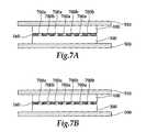
- FIGS. 7A and 7Aare cross sections showing before and after images of the substrate and semiconductor wafer being affixed to one another in accordance with the present invention.
- the present inventionprovides a substrate that can be combined with a semiconductor wafer to form a wafer-interposer that can be used to test semiconductor die prior to dicing or singulating. This allows several manufacturing steps to be eliminated and thus results in improved first pass yields, decreased manufacturing times, and improved cycle times. Additionally, the use of the wafer-interposer enables testing, such as parametric and burn-in, at the wafer level. Eliminating the need to singulate and package the dies before testing results in a significant cost avoidance opportunity for chip manufacturers. The fact that the use of the wafer-interposer accomplishes all of this while providing cost effective packaging is another substantial benefit of the present invention. The use of the B-stage adhesive substrate also eliminates the need to produce an extremely flat interposer to match well with the very flat semiconductor wafer.
- the substrate 100comprises a B-Stage laminate or adhesive material, and is shown suspended above a semiconductor die 140 .
- the first electrical contacts 110are shown in outline as they are on the lower surface of the substrate 100 .
- the first electrical pathways 130connect the first electrical contacts 110 to the second electrical contacts 120 , which are on the upper surface of the substrate 100 .
- the first and second electrical contacts 110 and 120can be connection pads.
- the substrate 100is then mounted on a semiconductor wafer.
- FIG. 1shows only a portion of the substrate 100 , and only a portion of the semiconductor wafer, i.e. a single semiconductor die 140 .
- Deposits of a conductor 150are applied to the third electrical contacts, which may be connection pads, on the dies that are included in the semiconductor wafer.
- the conductor 150can be any conductive adhesive. Examples include, but are not limited to, solder balls, conductive-polymer containing adhesives, and conductive plastics.
- a layer of no-flow underfill 160is applied to the first surface of the semiconductor wafer (and dies 140 ).
- FIG. 2shows a larger view of the top of a substrate 100 according to the present invention.
- the second electrical contacts 120are show as pads on the upper surface. In this depiction there are four sets of connections of nine contacts each. This would be connected to a wafer containing four dies. Clearly this is a very small number for demonstration purposes only, since actual semiconductor wafers can contain a much larger 15 number of dies.
- FIG. 3shows a side view of a semiconductor wafer 300 that is prepared for attachment to a substrate 100 (FIG. 2).
- the deposits of the conductors 150are shown, while the remaining surface of the semiconductor wafer 300 is covered by a layer of underfill 160 .
- the underfill 160is used to stabilize the assembly by resisting any lateral forces caused 20 by differences in the rates of thermal expansion between the semiconductor wafer 300 and the substrate 100 (FIG. 2).
- the underfill 160is applied over the entire semiconductor wafer 300 , but it is not immediately cured.
- the location of the second electrical contacts 120 on the upper surface of the substrate 100can be redistributed.
- the position of the second electrical contacts 120need not correspond directly to the position of the first electrical contacts 110 .
- the relocationcan take place on the surface of the semiconductor wafer (or die 140 ) as shown in FIG. 4.
- some of the third electrical contactshave been redistributed from their original locations (A) to different locations (B), by the application of additional metalization prior to depositing the conductors 150 (FIG. 3) and the underfill 160 (FIG. 3).
- FIG. 5shows a substrate 100 and a semiconductor wafer 300 prior to being attached to each other to form a wafer-interposer comprised of a substrate and semiconductor wafer assembly.
- the substrate 100still contains partially cured resins.
- the deposits of the conductor 150have been applied, as has the uncured underfill 160 .
- the semiconductor wafer 300is placed on a flat surface 500 .
- the substrate 100is mounted on another flat surface 510 that has been coated with a material to prevent adhesion of the substrate 100 . Suitable coating materials are known to those skilled in the art.
- the flat surfaces 500 and 510can be various materials and configurations. The primary requirement for the surfaces 500 and 510 is that they be substantially as planar as the semiconductor wafer 300 .
- a mechanism to bring the two surfaces 500 and 510 togetheris not shown, but would be known to those skilled in the art. Alignment of the semiconductor wafer 300 and the substrate 100 is accomplished by the use of split vision optics or any other comparable system. Prior to forming the assembly, the surface 510 can be heated to increase the malleability of the substrate 100 . The heating can be by accomplished by using forced air, heating coils, or any other method known in the industry.
- FIG. 6shows the semiconductor wafer 300 and the substrate 100 after they have been brought together to form an assembly.
- the entire assemblyis compressed.
- the conductors 150are solder balls whose nominal height is 0.006 inches
- the first surface of the semiconductor wafer 300 and the lower surface of the substrate 100could be brought to within 0.005 inches to insure proper contact. This would compensate for any variations in planarity of the surfaces or in the height of the conductors 150 .
- FIGS. 7A and 7Bshow the effects of compression.
- conductors 700 amake contact with the semiconductor wafer 100 ; whereas conductors 700 b do not make contact with the semiconductor wafer 100 . If the assembly were cured at this stage there would be missing connections. However, following compression, all contacts are properly made, as depicted in the FIG. 7B.
- the conductors 700 a and 700 bneed to be able to expand when they are compressed. The fact that the underfill 160 has not yet been cured allows this to happen.
- the wafer-interposer assemblyis cured. This can be accomplished while the compression is occurring, or after the assembly is removed from the flat surfaces 500 and 510 .
- the B-Stage laminate or adhesive of the substrate 100the conductors 150 and the underfill 160 are cured. As a result, the conductors 150 , 700 a and 700 b form permanent contacts with the third electrical contacts on the lower surface of the substrate 100 .
- the B-Stage laminate or adhesivemay form a rigid, semi-rigid or compliant bond.
- All semiconductor die 140 (FIG. 1) on the semiconductor wafer 300 (FIG. 7)can now be burned-in and electrically tested prior to dicing the semiconductor wafer 300 .
- the semiconductor diesare tested by attaching the substrate and semiconductor wafer assembly to a testing apparatus.
- the testingmay include parametric tests or burn-in tests.
- the testing of the semiconductor diescan be performed in sequence, in groups or simultaneously.
- the final stepis to dice the wafer-interposer assembly into individual devices or circuits.
- the wafer-interposer assemblymay also be diced into one or more semiconductor die groups.
- the substrate 100 for the wafer-interposer assemblyforms the package for the individual semiconductor die 140 (FIG. 1).
- the processmay also include grading one or more performance characteristics of each semiconductor die during testing and sorting the semiconductor chip assemblies based on the performance characteristics of the constituent dies.
- the semiconductor diesmay be sorted into conforming and nonconforming groups.
Landscapes
- Engineering & Computer Science (AREA)
- Computer Hardware Design (AREA)
- Microelectronics & Electronic Packaging (AREA)
- Power Engineering (AREA)
- Physics & Mathematics (AREA)
- Condensed Matter Physics & Semiconductors (AREA)
- General Physics & Mathematics (AREA)
- Manufacturing & Machinery (AREA)
- Testing Or Measuring Of Semiconductors Or The Like (AREA)
Abstract
Description
- The present invention relates generally to the field of integrated circuits, and more particularly, to a system, method and apparatus for constructing a semiconductor wafer-interposer using B-stage laminates.[0001]
- The three stages of semiconductor device manufacture are wafer fabrication, assembly and testing. The testing stage always includes an evaluation of the electrical connections within the device, and often includes burn-in testing as well. In a conventional manufacturing process, the semiconductor wafer is diced into individual semiconductor dies, and the dies are assembled into packages. The packages can be either the permanent type, for dies that are designed to be wire bonded into their packages, or they can be temporary, for chips that are designed to be mounted via flip-chip techniques. The purpose of the package is to protect the semiconductor die as well as provide connections that allow the package to be attached to a testing apparatus or printed circuit board. The fact that e final testing of the individual dies does not take place until the dies have been packaged, increases the cost. This increased cost stems from the greater complexity and size required of the testing apparatus, as well as the difficulty of manipulating large quantities of separately packaged dies.[0002]
- In addition to the tooling and labor costs associated with electrical and burn-in testing of individually packaged dies, there is also the wasted expense of packaging the dies that will subsequently be found to be defective. Since in a conventional process all dies must be packaged before final testing is done, this means that all defective die will necessarily be packaged, and the expense of doing so is complete waste. For example, if 6%, a conservative estimate, of the dies fail either the electrical or burn-in testing, then 60 die packaging operations are wasted for every 1000 dies that are produced. The ability to test the dies before the packaging operations would obviously reduce production costs.[0003]
- The savings associated with a wafer level testing protocol are multifold. In addition to the savings associated with the elimination of unnecessary packaging operations, inventory carrying costs are reduced because the processing cycle times are reduced since “good” dies are identified earlier in the manufacturing process.[0004]
- Accordingly, there is a need for a wafer-interposer and a method that allows for the testing of semiconductor dies while still assembled in wafer form. It is also important that the wafer-interposer and method does not impede the ability to package, or directly mount the dies after they have passed the testing, and have been cut from the wafer. Additionally, a wafer-interposer that compensates for surface imperfections related to the semiconductor wafer and eliminates the need to produce an extremely flat interposer is desired.[0005]
- The present invention provides a substrate that can be combined with a semiconductor wafer to form a wafer-interposer that can be used to test semiconductor die prior to dicing or singulating. This allows several manufacturing steps to be eliminated and thus results in improved first pass yields, decreased manufacturing times, and improved cycle times. Additionally, the use of the wafer-interposer enables testing, such as parametric and burn-in, at the wafer level. Eliminating the need to singulate and package the dies before testing results in a significant cost avoidance opportunity for chip manufacturers. The fact that the use of the wafer-interposer accomplishes all of this while providing cost effective packaging is another substantial benefit of the present invention. The use of the B-stage adhesive substrate also eliminates the need to produce an extremely flat interposer to match well with the very flat semiconductor wafer.[0006]
- The present invention provides, in one form, a substrate comprising a B-Stage laminate or adhesive material and having an upper and a lower surface. The substrate has one or more first electrical contacts on the lower surface, and one or more second electrical contacts on the upper surface. The second electrical contacts have greater surface area and greater pitch than the first electrical contacts. One or more first electrical pathways pass through the substrate and connect the first electrical contacts to the second electrical contacts.[0007]
- Another form of the present invention provides a substrate and semiconductor wafer assembly having a substrate comprised of a B-Stage laminate or adhesive material, a semiconductor wafer and a layer of no-flow underfill disposed between the substrate and the semiconductor wafer. The substrate has an upper and a lower surface, one or more first electrical contacts on the lower surface, and one or more second electrical contacts on the upper surface. The second electrical contacts have a greater surface area and greater pitch than the first electrical contacts. In addition, one or more first electrical pathways pass through the substrate and connect the first electrical contacts to the second electrical contacts. The semiconductor wafer includes one or more semiconductor dies, and has a first and a second surface. The semiconductor wafer also has one or more third electrical contacts on the first surface, the third electrical contacts being associated with the semiconductor dies. A conductor electrically connects each of the first electrical contacts with a corresponding third electrical contact.[0008]
- Yet another form of the present invention provides a method for producing a semiconductor wafer-interposer. One or more first electrical contacts are attached to the lower surface of a substrate comprising a B-Stage adhesive material. One or more second electrical contacts are attached to an upper surface of the substrate. The second electrical contacts have a greater surface area and greater pitch than the first electrical contacts. One or more first electrical pathways are created to pass through the substrate and connect the first electrical contacts to the second electrical contacts.[0009]
- In still another form, the present invention provides a method for producing a wafer-interposer assembly. One or more first electrical contacts are attached to the lower surface of a substrate comprising a B-Stage adhesive material. One or more second electrical contacts are attached to an upper surface of the substrate. The second electrical contacts have greater surface area and greater pitch than the first electrical contacts. One or more first electrical pathways are created to pass through the substrate and connect the first electrical contacts to the second electrical contacts. A conductor is deposited on one or more third electrical contacts on an upper surface of a semiconductor wafer. The semiconductor wafer includes one or more semiconductor dies and the third electrical contacts are associated with the semiconductor dies. A layer of no-flow underfill is applied to the upper surface of the semiconductor wafer. The substrate is aligned with the semiconductor wafer so that the conductors on the third electrical contacts of the semiconductor wafer correspond to the first electrical contacts on the lower surface of the substrate. The substrate is then attached to the semiconductor wafer.[0010]
- The above and further advantages of the invention may be better understood by referring to the following description in conjunction with the accompanying drawings in which corresponding numerals in the different figures refer to the corresponding parts in which:[0011]
- FIG. 1 is an exploded view of a wafer testing interposer and semiconductor die in accordance with the present invention;[0012]
- FIG. 2 shows the upper surface of a substrate in accordance with the present invention;[0013]
- FIG. 3 is a cross section of a semiconductor wafer prepared for bonding to a wafer testing interposer in accordance with the present invention;[0014]
- FIG. 4 shows the top of a semiconductor die that has had some of the electrical contacts redistributed in accordance with the present invention;[0015]
- FIG. 5 is a cross section of a substrate and semiconductor wafer, each mounted on a flat surface in preparation for being affixed to one another in accordance with the present invention;[0016]
- FIG. 6 is a cross section of a substrate and semiconductor wafer, each mounted on a flat surface, after they have been affixed to one another in accordance with the present invention; and[0017]
- FIGS. 7A and 7A are cross sections showing before and after images of the substrate and semiconductor wafer being affixed to one another in accordance with the present invention.[0018]
- While the making and using of various embodiments of the present invention are discussed herein in terms of a wafer testing interposer and semiconductor wafer assembly apparatus and method, it should be appreciated that the present invention provides many inventive concepts that can be embodied in a wide variety of contexts. The specific embodiments discussed herein are merely illustrative of specific ways to make and use the invention, and are in no way meant to limit the scope of the invention.[0019]
- The present invention provides a substrate that can be combined with a semiconductor wafer to form a wafer-interposer that can be used to test semiconductor die prior to dicing or singulating. This allows several manufacturing steps to be eliminated and thus results in improved first pass yields, decreased manufacturing times, and improved cycle times. Additionally, the use of the wafer-interposer enables testing, such as parametric and burn-in, at the wafer level. Eliminating the need to singulate and package the dies before testing results in a significant cost avoidance opportunity for chip manufacturers. The fact that the use of the wafer-interposer accomplishes all of this while providing cost effective packaging is another substantial benefit of the present invention. The use of the B-stage adhesive substrate also eliminates the need to produce an extremely flat interposer to match well with the very flat semiconductor wafer.[0020]
- The general features of the substrate for the wafer-interposer of the present invention are shown in FIG. 1. The[0021]
substrate 100 comprises a B-Stage laminate or adhesive material, and is shown suspended above asemiconductor die 140. The firstelectrical contacts 110 are shown in outline as they are on the lower surface of thesubstrate 100. The firstelectrical pathways 130 connect the firstelectrical contacts 110 to the secondelectrical contacts 120, which are on the upper surface of thesubstrate 100. The first and secondelectrical contacts substrate 100 is then mounted on a semiconductor wafer. FIG. 1 shows only a portion of thesubstrate 100, and only a portion of the semiconductor wafer, i.e. asingle semiconductor die 140. Deposits of aconductor 150 are applied to the third electrical contacts, which may be connection pads, on the dies that are included in the semiconductor wafer. Theconductor 150 can be any conductive adhesive. Examples include, but are not limited to, solder balls, conductive-polymer containing adhesives, and conductive plastics. A layer of no-flow underfill 160 is applied to the first surface of the semiconductor wafer (and dies140). - FIG. 2 shows a larger view of the top of a[0022]
substrate 100 according to the present invention. The secondelectrical contacts 120 are show as pads on the upper surface. In this depiction there are four sets of connections of nine contacts each. This would be connected to a wafer containing four dies. Clearly this is a very small number for demonstration purposes only, since actual semiconductor wafers can contain a much larger15 number of dies. - FIG. 3 shows a side view of a[0023]
semiconductor wafer 300 that is prepared for attachment to a substrate100 (FIG. 2). The deposits of theconductors 150 are shown, while the remaining surface of thesemiconductor wafer 300 is covered by a layer ofunderfill 160. Theunderfill 160 is used to stabilize the assembly by resisting any lateral forces caused20 by differences in the rates of thermal expansion between thesemiconductor wafer 300 and the substrate100 (FIG. 2). Theunderfill 160 is applied over theentire semiconductor wafer 300, but it is not immediately cured. - As shown in FIG. 1, the location of the second[0024]
electrical contacts 120 on the upper surface of thesubstrate 100 can be redistributed. In other words, the position of the secondelectrical contacts 120 need not correspond directly to the position of the firstelectrical contacts 110. As an alternative, the relocation can take place on the surface of the semiconductor wafer (or die140) as shown in FIG. 4. In FIG. 4 some of the third electrical contacts have been redistributed from their original locations (A) to different locations (B), by the application of additional metalization prior to depositing the conductors150 (FIG. 3) and the underfill160 (FIG. 3). - FIG. 5 shows a[0025]
substrate 100 and asemiconductor wafer 300 prior to being attached to each other to form a wafer-interposer comprised of a substrate and semiconductor wafer assembly. At this stage, thesubstrate 100 still contains partially cured resins. The deposits of theconductor 150 have been applied, as has theuncured underfill 160. Prior to assembly, thesemiconductor wafer 300 is placed on aflat surface 500. Thesubstrate 100 is mounted on anotherflat surface 510 that has been coated with a material to prevent adhesion of thesubstrate 100. Suitable coating materials are known to those skilled in the art. Theflat surfaces surfaces semiconductor wafer 300. A mechanism to bring the twosurfaces semiconductor wafer 300 and thesubstrate 100 is accomplished by the use of split vision optics or any other comparable system. Prior to forming the assembly, thesurface 510 can be heated to increase the malleability of thesubstrate 100. The heating can be by accomplished by using forced air, heating coils, or any other method known in the industry. - FIG. 6 shows the[0026]
semiconductor wafer 300 and thesubstrate 100 after they have been brought together to form an assembly. To insure that 100% of the electrical contacts are formed between the deposits of theconductors 150 and the firstelectrical contacts 110 on the lower surface of thesubstrate 100, the entire assembly is compressed. For example, if theconductors 150 are solder balls whose nominal height is 0.006 inches, then the first surface of thesemiconductor wafer 300 and the lower surface of thesubstrate 100 could be brought to within 0.005 inches to insure proper contact. This would compensate for any variations in planarity of the surfaces or in the height of theconductors 150. - FIGS. 7A and 7B show the effects of compression. Before compression,[0027]
conductors 700amake contact with thesemiconductor wafer 100; whereasconductors 700bdo not make contact with thesemiconductor wafer 100. If the assembly were cured at this stage there would be missing connections. However, following compression, all contacts are properly made, as depicted in the FIG. 7B. In order for compression to work, theconductors underfill 160 has not yet been cured allows this to happen. - After the constituent parts are joined, the wafer-interposer assembly is cured. This can be accomplished while the compression is occurring, or after the assembly is removed from the[0028]
flat surfaces substrate 100, theconductors 150 and theunderfill 160 are cured. As a result, theconductors substrate 100. The B-Stage laminate or adhesive may form a rigid, semi-rigid or compliant bond. - All semiconductor die[0029]140 (FIG. 1) on the semiconductor wafer300 (FIG. 7) can now be burned-in and electrically tested prior to dicing the
semiconductor wafer 300. The semiconductor dies are tested by attaching the substrate and semiconductor wafer assembly to a testing apparatus. The testing may include parametric tests or burn-in tests. In addition, the testing of the semiconductor dies can be performed in sequence, in groups or simultaneously. - The final step is to dice the wafer-interposer assembly into individual devices or circuits. The wafer-interposer assembly may also be diced into one or more semiconductor die groups. The[0030]
substrate 100 for the wafer-interposer assembly forms the package for the individual semiconductor die140 (FIG. 1). The process may also include grading one or more performance characteristics of each semiconductor die during testing and sorting the semiconductor chip assemblies based on the performance characteristics of the constituent dies. In addition, the semiconductor dies may be sorted into conforming and nonconforming groups. - The embodiments and examples set forth herein are presented to best explain the present invention and its practical application and to thereby enable those skilled in the art to make and utilize the invention. Those skilled in the art, however, will recognize that the foregoing description and examples have been presented for the purpose of illustration and example only. Other variations and modifications of the present invention will be apparent to those of skill in the art, and it is the intent of the appended claims that such variations and modifications be covered. The description as set forth is not intended to be exhaustive or to limit the scope of the invention. Many modifications and variations are possible in light of the above teaching without departing from the spirit and scope of the following claims. It is contemplated that the use of the present invention can involve components having different characteristics. It is intended that the scope of the present invention be defined by the claims appended hereto, giving full cognizance to equivalents in all respects.[0031]
Claims (31)
1. An interposer comprising:
a substrate comprising a B-stage adhesive material, and having an upper surface and a lower surface;
one or more first electrical contacts on the lower surface;
one or more second electrical contacts on the upper surface, the second electrical contacts having greater surface area, and greater pitch than the first electrical contacts; and
one or more first electrical pathways passing through the substrate, and connecting the first electrical contacts to the second electrical contacts.
2. The interposer as recited inclaim 1 wherein the first and second electrical contacts are connection pads.
3. A substrate and semiconductor wafer assembly comprising:
a substrate comprising a B-stage adhesive material, and having an upper surface and a lower surface, one or more first electrical contacts on the lower surface, one or more second electrical contacts on the upper surface, the second electrical contacts having greater surface area and greater pitch than the first electrical contacts, one or more first electrical pathways passing through the substrate, and connecting the first electrical contacts to the second electrical contacts.
a semiconductor wafer including one or more semiconductor dies, and having a first surface and a second surface, one or more third electrical contacts on the first surface of the semiconductor wafer, the third electrical contacts being associated with the semiconductor dies;
a conductor electrically connecting each first electrical contact with a corresponding third electrical contact; and
a layer of no-flow underfill disposed between the first surface of the semiconductor wafer and the lower surface of the substrate.
4. The substrate and semiconductor wafer assembly as recited inclaim 3 wherein the first, second and third electrical contacts are connection pads.
5. The substrate and semiconductor wafer assembly as recited inclaim 3 wherein each conductor is a solder ball.
6. The substrate and semiconductor wafer assembly as recited inclaim 3 wherein each conductor comprises a conductive-polymer containing adhesive.
7. The substrate and semiconductor wafer assembly as recited inclaim 3 wherein each conductor comprises a conductive plastic.
8. A method of producing a semiconductor wafer-interposer comprising the steps of:
attaching one or more first electrical contacts to a lower surface of a substrate comprising a B-Stage adhesive material;
attaching one or more second electrical contacts to an upper surface of the substrate, the second electrical contacts having greater surface area and greater pitch than the first electrical contacts; and
creating one or more first electrical pathways passing through the substrate and connecting the first electrical contacts to the second electrical contacts.
9. The method as recited inclaim 8 , wherein the first and second electrical contacts are connection pads.
10. A method for producing a wafer-interposer assembly comprising the steps of:
attaching one or more first electrical contacts to a lower surface of a substrate, the substrate comprising a B-Stage adhesive material;
attaching one or more second electrical contacts to an upper surface of the substrate, the second electrical contacts having greater surface area and greater pitch than the first electrical contacts;
creating one or more first electrical pathways passing through the substrate and connecting the first electrical contacts to the second electrical contacts;
depositing a conductor on one or more third electrical contacts on an upper surface of a semiconductor wafer, the semiconductor wafer including one or more semiconductor dies and the third electrical contacts being associated with the semiconductor dies;
applying a layer of no-flow underfill to the upper surface of the semiconductor wafer;
aligning the substrate with the semiconductor wafer so that the deposits of the conductor on the third electrical contacts correspond with the first electrical contacts on the lower surface of the substrate;
attaching the substrate to the semiconductor wafer.
11. The method as recited inclaim 10 wherein the first, second and third electrical contacts are connection pads.
12. The method as recited inclaim 10 further comprising the step of curing the B-Stage adhesive, the conductors, and the underfill.
13. The method as recited inclaim 10 further comprising the step of applying additional metalization to one or more of the third electrical contacts to redistribute them prior to the attachment of the substrate.
14. The method as recited inclaim 10 further comprising the step of adding additional metalization to one or more of the third electrical contacts to improve the contact between the conductor and the third electrical contacts.
15. The method as recited inclaim 10 where in the step of attaching the substrate to the semiconductor wafer comprises the steps of:
placing the semiconductor wafer on a first flat surface and holding the semiconductor wafer in place;
coating a second flat surface with a material that will prevent adhesion of the substrate;
placing the substrate on the second flat surface and holding the substrate in place; and
bringing the first and second flat surfaces together so that the semiconductor wafer and the substrate form an adhesive bond.
16. The method as recited inclaim 10 further comprising the step of singulating the substrate and semiconductor wafer assembly into one or more semiconductor die assemblies.
17. The method as recited inclaim 10 wherein the cured B-Stage adhesive forms a rigid bond.
18. The method as recited inclaim 10 wherein the cured B-stage adhesive forms a semi-rigid bond.
19. The method as recited inclaim 10 wherein the cured B-Stage adhesive forms a compliant bond.
20. The method as recited inclaim 10 wherein each conductor is a solder ball.
21. The method as recited inclaim 10 wherein each conductor comprises a conductive-polymer adhesive.
22. The method as recited inclaim 10 wherein each conductor comprises a conductive plastic.
23. The method as recited inclaim 10 further comprising the steps:
attaching the substrate and semiconductor wafer assembly to a testing apparatus; and
testing at least one of the semiconductor dies.
24. The method as recited inclaim 23 wherein the step of testing the semiconductor dies further comprises performing parametric testing on at least one of the dies.
25. The method as recited inclaim 23 wherein the step of testing the semiconductor dies further comprises performing burn-in testing on at least one of the dies.
26. The method as recited inclaim 23 wherein the step of testing the semiconductor dies further comprises testing the semiconductor dies in sequence.
27. The method as recited inclaim 23 wherein the step of testing the semiconductor dies further comprises testing the semiconductor dies simultaneously.
28. The method as recited inclaim 23 further comprising the step of grading one or more performance characteristics of each semiconductor die during testing.
29. The method as recited inclaim 28 further comprising the step of singulating the substrate and semiconductor wafer assembly into one or more semiconductor die assemblies.
30. The method as recited inclaim 29 further comprising the step of sorting the semiconductor die assemblies based on the one or more performance characteristics.
31. The method as recited inclaim 29 further comprising the step of sorting the semiconductor die assemblies into conforming and nonconforming groups.
Priority Applications (1)
| Application Number | Priority Date | Filing Date | Title |
|---|---|---|---|
| US09/738,193US20020076854A1 (en) | 2000-12-15 | 2000-12-15 | System, method and apparatus for constructing a semiconductor wafer-interposer using B-Stage laminates |
Applications Claiming Priority (1)
| Application Number | Priority Date | Filing Date | Title |
|---|---|---|---|
| US09/738,193US20020076854A1 (en) | 2000-12-15 | 2000-12-15 | System, method and apparatus for constructing a semiconductor wafer-interposer using B-Stage laminates |
Publications (1)
| Publication Number | Publication Date |
|---|---|
| US20020076854A1true US20020076854A1 (en) | 2002-06-20 |
Family
ID=24966947
Family Applications (1)
| Application Number | Title | Priority Date | Filing Date |
|---|---|---|---|
| US09/738,193AbandonedUS20020076854A1 (en) | 2000-12-15 | 2000-12-15 | System, method and apparatus for constructing a semiconductor wafer-interposer using B-Stage laminates |
Country Status (1)
| Country | Link |
|---|---|
| US (1) | US20020076854A1 (en) |
Cited By (5)
| Publication number | Priority date | Publication date | Assignee | Title |
|---|---|---|---|---|
| US20020061011A1 (en)* | 2000-09-07 | 2002-05-23 | Sbc Technology Resources, Inc. | Internal substitution bi-level addressing for compatible public networks |
| US20040185601A1 (en)* | 2003-03-18 | 2004-09-23 | Frank Stepniak | Wafer-applied underfill process |
| US20050017256A1 (en)* | 2001-07-23 | 2005-01-27 | Slater David B. | Flip-chip bonding of light emitting devices |
| US20070063325A1 (en)* | 2005-09-22 | 2007-03-22 | Chun-Hung Lin | Chip package structure and bumping process |
| WO2009129136A3 (en)* | 2008-04-16 | 2010-01-21 | Henkel Corporation | Flow controllable b-stageable composition |
Citations (91)
| Publication number | Priority date | Publication date | Assignee | Title |
|---|---|---|---|---|
| US3939588A (en)* | 1974-06-24 | 1976-02-24 | Hockaday Robert C | Lettering guide apparatus |
| US4577214A (en)* | 1981-05-06 | 1986-03-18 | At&T Bell Laboratories | Low-inductance power/ground distribution in a package for a semiconductor chip |
| US4617730A (en)* | 1984-08-13 | 1986-10-21 | International Business Machines Corporation | Method of fabricating a chip interposer |
| US4628411A (en)* | 1984-03-12 | 1986-12-09 | International Business Machines Corporation | Apparatus for directly powering a multi-chip module from a power distribution bus |
| US4688151A (en)* | 1986-03-10 | 1987-08-18 | International Business Machines Corporation | Multilayered interposer board for powering high current chip modules |
| US4868712A (en)* | 1987-02-04 | 1989-09-19 | Woodman John K | Three dimensional integrated circuit package |
| US4998885A (en)* | 1989-10-27 | 1991-03-12 | International Business Machines Corporation | Elastomeric area array interposer |
| US5016138A (en)* | 1987-10-27 | 1991-05-14 | Woodman John K | Three dimensional integrated circuit package |
| US5060052A (en)* | 1990-09-04 | 1991-10-22 | Motorola, Inc. | TAB bonded semiconductor device having off-chip power and ground distribution |
| US5065227A (en)* | 1990-06-04 | 1991-11-12 | International Business Machines Corporation | Integrated circuit packaging using flexible substrate |
| US5068558A (en)* | 1988-10-07 | 1991-11-26 | Nippon Ferrofluidics Corporation | Magnetic bearing device |
| US5123850A (en)* | 1990-04-06 | 1992-06-23 | Texas Instruments Incorporated | Non-destructive burn-in test socket for integrated circuit die |
| US5132613A (en)* | 1990-11-30 | 1992-07-21 | International Business Machines Corporation | Low inductance side mount decoupling test structure |
| US5148265A (en)* | 1990-09-24 | 1992-09-15 | Ist Associates, Inc. | Semiconductor chip assemblies with fan-in leads |
| US5148266A (en)* | 1990-09-24 | 1992-09-15 | Ist Associates, Inc. | Semiconductor chip assemblies having interposer and flexible lead |
| US5309021A (en)* | 1991-10-16 | 1994-05-03 | Mitsubishi Denki Kabushiki Kaisha | Semiconductor device having particular power distribution interconnection arrangement |
| US5327325A (en)* | 1993-02-08 | 1994-07-05 | Fairchild Space And Defense Corporation | Three-dimensional integrated circuit package |
| US5347162A (en)* | 1989-08-28 | 1994-09-13 | Lsi Logic Corporation | Preformed planar structures employing embedded conductors |
| US5371654A (en)* | 1992-10-19 | 1994-12-06 | International Business Machines Corporation | Three dimensional high performance interconnection package |
| US5382898A (en)* | 1992-09-21 | 1995-01-17 | Cerprobe Corporation | High density probe card for testing electrical circuits |
| US5384691A (en)* | 1993-01-08 | 1995-01-24 | General Electric Company | High density interconnect multi-chip modules including embedded distributed power supply elements |
| US5394303A (en)* | 1992-09-11 | 1995-02-28 | Kabushiki Kaisha Toshiba | Semiconductor device |
| US5399505A (en)* | 1993-07-23 | 1995-03-21 | Motorola, Inc. | Method and apparatus for performing wafer level testing of integrated circuit dice |
| US5399898A (en)* | 1992-07-17 | 1995-03-21 | Lsi Logic Corporation | Multi-chip semiconductor arrangements using flip chip dies |
| US5410259A (en)* | 1992-06-01 | 1995-04-25 | Tokyo Electron Yamanashi Limited | Probing device setting a probe card parallel |
| US5477160A (en)* | 1992-08-12 | 1995-12-19 | Fujitsu Limited | Module test card |
| US5476211A (en)* | 1993-11-16 | 1995-12-19 | Form Factor, Inc. | Method of manufacturing electrical contacts, using a sacrificial member |
| US5483421A (en)* | 1992-03-09 | 1996-01-09 | International Business Machines Corporation | IC chip attachment |
| US5489804A (en)* | 1989-08-28 | 1996-02-06 | Lsi Logic Corporation | Flexible preformed planar structures for interposing between a chip and a substrate |
| US5491612A (en)* | 1995-02-21 | 1996-02-13 | Fairchild Space And Defense Corporation | Three-dimensional modular assembly of integrated circuits |
| US5497079A (en)* | 1992-09-01 | 1996-03-05 | Matsushita Electric Industrial Co., Ltd. | Semiconductor testing apparatus, semiconductor testing circuit chip, and probe card |
| US5517515A (en)* | 1994-08-17 | 1996-05-14 | International Business Machines Corporation | Multichip module with integrated test circuitry disposed within interposer substrate |
| US5518964A (en)* | 1994-07-07 | 1996-05-21 | Tessera, Inc. | Microelectronic mounting with multiple lead deformation and bonding |
| US5532612A (en)* | 1994-07-19 | 1996-07-02 | Liang; Louis H. | Methods and apparatus for test and burn-in of integrated circuit devices |
| US5544017A (en)* | 1992-08-05 | 1996-08-06 | Fujitsu Limited | Multichip module substrate |
| US5570032A (en)* | 1993-08-17 | 1996-10-29 | Micron Technology, Inc. | Wafer scale burn-in apparatus and process |
| US5579207A (en)* | 1994-10-20 | 1996-11-26 | Hughes Electronics | Three-dimensional integrated circuit stacking |
| US5594273A (en)* | 1993-07-23 | 1997-01-14 | Motorola Inc. | Apparatus for performing wafer-level testing of integrated circuits where test pads lie within integrated circuit die but overly no active circuitry for improved yield |
| US5600257A (en)* | 1995-08-09 | 1997-02-04 | International Business Machines Corporation | Semiconductor wafer test and burn-in |
| US5600541A (en)* | 1993-12-08 | 1997-02-04 | Hughes Aircraft Company | Vertical IC chip stack with discrete chip carriers formed from dielectric tape |
| US5612575A (en)* | 1994-05-20 | 1997-03-18 | Matra Marconi Space France | Method of connecting the output pads on an integrated circuit chip, and multichip module thus obtained |
| US5615089A (en)* | 1994-07-26 | 1997-03-25 | Fujitsu Limited | BGA semiconductor device including a plurality of semiconductor chips located on upper and lower surfaces of a first substrate |
| US5635101A (en)* | 1996-01-22 | 1997-06-03 | Janke George A | Deicing composition and method |
| US5637920A (en)* | 1995-10-04 | 1997-06-10 | Lsi Logic Corporation | High contact density ball grid array package for flip-chips |
| US5654588A (en)* | 1993-07-23 | 1997-08-05 | Motorola Inc. | Apparatus for performing wafer-level testing of integrated circuits where the wafer uses a segmented conductive top-layer bus structure |
| US5655290A (en)* | 1992-08-05 | 1997-08-12 | Fujitsu Limited | Method for making a three-dimensional multichip module |
| US5685885A (en)* | 1990-09-24 | 1997-11-11 | Tessera, Inc. | Wafer-scale techniques for fabrication of semiconductor chip assemblies |
| US5701666A (en)* | 1994-08-31 | 1997-12-30 | Motorola, Inc. | Method for manufacturing a stimulus wafer for use in a wafer-to-wafer testing system to test integrated circuits located on a product wafer |
| US5710071A (en)* | 1995-12-04 | 1998-01-20 | Motorola, Inc. | Process for underfilling a flip-chip semiconductor device |
| US5714800A (en)* | 1996-03-21 | 1998-02-03 | Motorola, Inc. | Integrated circuit assembly having a stepped interposer and method |
| US5759047A (en)* | 1996-05-24 | 1998-06-02 | International Business Machines Corporation | Flexible circuitized interposer with apertured member and method for making same |
| US5764071A (en)* | 1996-01-05 | 1998-06-09 | International Business Machines Corporation | Method and system for testing an electronic module mounted on a printed circuit board |
| US5789807A (en)* | 1996-10-15 | 1998-08-04 | International Business Machines Corporation | On-chip power distribution for improved decoupling |
| US5794175A (en)* | 1997-09-09 | 1998-08-11 | Teradyne, Inc. | Low cost, highly parallel memory tester |
| US5796746A (en)* | 1995-12-22 | 1998-08-18 | Micron Technology, Inc. | Device and method for testing integrated circuit dice in an integrated circuit module |
| US5798652A (en)* | 1993-11-23 | 1998-08-25 | Semicoa Semiconductors | Method of batch testing surface mount devices using a substrate edge connector |
| US5800184A (en)* | 1994-03-08 | 1998-09-01 | International Business Machines Corporation | High density electrical interconnect apparatus and method |
| US5805422A (en)* | 1994-09-21 | 1998-09-08 | Nec Corporation | Semiconductor package with flexible board and method of fabricating the same |
| US5802713A (en)* | 1995-01-20 | 1998-09-08 | Fairchild Space And Defense Corportion | Circuit board manufacturing method |
| US5806181A (en)* | 1993-11-16 | 1998-09-15 | Formfactor, Inc. | Contact carriers (tiles) for populating larger substrates with spring contacts |
| US5821624A (en)* | 1989-08-28 | 1998-10-13 | Lsi Logic Corporation | Semiconductor device assembly techniques using preformed planar structures |
| US5834946A (en)* | 1995-10-19 | 1998-11-10 | Mosaid Technologies Incorporated | Integrated circuit test head |
| US5834844A (en)* | 1995-03-24 | 1998-11-10 | Shinko Electric Industries Co., Ltd. | Semiconductor device having an element with circuit pattern thereon |
| US5832601A (en)* | 1993-11-16 | 1998-11-10 | Form Factor, Inc. | Method of making temporary connections between electronic components |
| US5838072A (en)* | 1997-02-24 | 1998-11-17 | Mosel Vitalic Corporation | Intrachip power distribution package and method for semiconductors having a supply node electrically interconnected with one or more intermediate nodes |
| US5838060A (en)* | 1995-12-12 | 1998-11-17 | Comer; Alan E. | Stacked assemblies of semiconductor packages containing programmable interconnect |
| US5844803A (en)* | 1997-02-17 | 1998-12-01 | Micron Technology, Inc. | Method of sorting a group of integrated circuit devices for those devices requiring special testing |
| US5854507A (en)* | 1998-07-21 | 1998-12-29 | Hewlett-Packard Company | Multiple chip assembly |
| US5878486A (en)* | 1993-11-16 | 1999-03-09 | Formfactor, Inc. | Method of burning-in semiconductor devices |
| US5942795A (en)* | 1997-07-03 | 1999-08-24 | National Semiconductor Corporation | Leaded substrate carrier for integrated circuit device and leaded substrate carrier device assembly |
| US6013944A (en)* | 1997-02-10 | 2000-01-11 | Fujitsu Limited | Semiconductor device in which chip electrodes are connected to terminals arranged along the periphery of an insulative board |
| US6018462A (en)* | 1997-06-30 | 2000-01-25 | Nec Corporation | Multi-tip module |
| US6229216B1 (en)* | 1999-01-11 | 2001-05-08 | Intel Corporation | Silicon interposer and multi-chip-module (MCM) with through substrate vias |
| US6297553B1 (en)* | 1998-10-30 | 2001-10-02 | Shinko Electric Industries Co., Ltd | Semiconductor device and process for producing the same |
| US6376769B1 (en)* | 1999-05-18 | 2002-04-23 | Amerasia International Technology, Inc. | High-density electronic package, and method for making same |
| US6387830B1 (en)* | 1997-06-13 | 2002-05-14 | International Business Machines Corporation | Method for reducing coefficient of thermal expansion in chip attach packages |
| US6400019B1 (en)* | 1999-11-25 | 2002-06-04 | Hitachi, Ltd. | Semiconductor device with wiring substrate |
| US6426548B1 (en)* | 1998-03-18 | 2002-07-30 | Hitachi Cable Ltd. | Semiconductor device, lead-patterning substrate, and electronics device, and method for fabricating same |
| US6458681B1 (en)* | 1996-03-07 | 2002-10-01 | Tessera, Inc. | Method for providing void free layer for semiconductor assemblies |
| US6483043B1 (en)* | 2000-05-19 | 2002-11-19 | Eaglestone Partners I, Llc | Chip assembly with integrated power distribution between a wafer interposer and an integrated circuit chip |
| US6489180B1 (en)* | 2000-09-28 | 2002-12-03 | Siliconware Precision Industries Co., Ltd. | Flip-chip packaging process utilizing no-flow underfill technique |
| US20030041451A1 (en)* | 1999-03-10 | 2003-03-06 | Masud Beroz | Microelectronic joining processes |
| US6534875B1 (en)* | 1998-09-25 | 2003-03-18 | Sony Corporation | Semiconductor part for component mounting, mounting structure and mounting method |
| US6537831B1 (en)* | 2000-07-31 | 2003-03-25 | Eaglestone Partners I, Llc | Method for selecting components for a matched set using a multi wafer interposer |
| US6555469B1 (en)* | 1998-03-20 | 2003-04-29 | Microcsp, Inc. | Chip scale packages |
| US6586822B1 (en)* | 2000-09-08 | 2003-07-01 | Intel Corporation | Integrated core microelectronic package |
| US6627998B1 (en)* | 2000-07-27 | 2003-09-30 | International Business Machines Corporation | Wafer scale thin film package |
| US6717819B1 (en)* | 1999-06-01 | 2004-04-06 | Amerasia International Technology, Inc. | Solderable flexible adhesive interposer as for an electronic package, and method for making same |
| US6730541B2 (en)* | 1997-11-20 | 2004-05-04 | Texas Instruments Incorporated | Wafer-scale assembly of chip-size packages |
| US6812048B1 (en)* | 2000-07-31 | 2004-11-02 | Eaglestone Partners I, Llc | Method for manufacturing a wafer-interposer assembly |
| US6822469B1 (en)* | 2000-07-31 | 2004-11-23 | Eaglestone Partners I, Llc | Method for testing multiple semiconductor wafers |
- 2000
- 2000-12-15USUS09/738,193patent/US20020076854A1/ennot_activeAbandoned
Patent Citations (98)
| Publication number | Priority date | Publication date | Assignee | Title |
|---|---|---|---|---|
| US3939588A (en)* | 1974-06-24 | 1976-02-24 | Hockaday Robert C | Lettering guide apparatus |
| US4577214A (en)* | 1981-05-06 | 1986-03-18 | At&T Bell Laboratories | Low-inductance power/ground distribution in a package for a semiconductor chip |
| US4628411A (en)* | 1984-03-12 | 1986-12-09 | International Business Machines Corporation | Apparatus for directly powering a multi-chip module from a power distribution bus |
| US4617730A (en)* | 1984-08-13 | 1986-10-21 | International Business Machines Corporation | Method of fabricating a chip interposer |
| US4688151A (en)* | 1986-03-10 | 1987-08-18 | International Business Machines Corporation | Multilayered interposer board for powering high current chip modules |
| US4868712A (en)* | 1987-02-04 | 1989-09-19 | Woodman John K | Three dimensional integrated circuit package |
| US5016138A (en)* | 1987-10-27 | 1991-05-14 | Woodman John K | Three dimensional integrated circuit package |
| US5068558A (en)* | 1988-10-07 | 1991-11-26 | Nippon Ferrofluidics Corporation | Magnetic bearing device |
| US5489804A (en)* | 1989-08-28 | 1996-02-06 | Lsi Logic Corporation | Flexible preformed planar structures for interposing between a chip and a substrate |
| US5347162A (en)* | 1989-08-28 | 1994-09-13 | Lsi Logic Corporation | Preformed planar structures employing embedded conductors |
| US5821624A (en)* | 1989-08-28 | 1998-10-13 | Lsi Logic Corporation | Semiconductor device assembly techniques using preformed planar structures |
| US4998885A (en)* | 1989-10-27 | 1991-03-12 | International Business Machines Corporation | Elastomeric area array interposer |
| US5123850A (en)* | 1990-04-06 | 1992-06-23 | Texas Instruments Incorporated | Non-destructive burn-in test socket for integrated circuit die |
| US5065227A (en)* | 1990-06-04 | 1991-11-12 | International Business Machines Corporation | Integrated circuit packaging using flexible substrate |
| US5060052A (en)* | 1990-09-04 | 1991-10-22 | Motorola, Inc. | TAB bonded semiconductor device having off-chip power and ground distribution |
| US5148266A (en)* | 1990-09-24 | 1992-09-15 | Ist Associates, Inc. | Semiconductor chip assemblies having interposer and flexible lead |
| US6433419B2 (en)* | 1990-09-24 | 2002-08-13 | Tessera, Inc. | Face-up semiconductor chip assemblies |
| US5347159A (en)* | 1990-09-24 | 1994-09-13 | Tessera, Inc. | Semiconductor chip assemblies with face-up mounting and rear-surface connection to substrate |
| US20020011663A1 (en)* | 1990-09-24 | 2002-01-31 | Khandros Igor Y. | Face-up semiconductor chip assemblies |
| US6133627A (en)* | 1990-09-24 | 2000-10-17 | Tessera, Inc. | Semiconductor chip package with center contacts |
| US5848467A (en)* | 1990-09-24 | 1998-12-15 | Tessera, Inc. | Methods of making semiconductor chip assemblies |
| US5685885A (en)* | 1990-09-24 | 1997-11-11 | Tessera, Inc. | Wafer-scale techniques for fabrication of semiconductor chip assemblies |
| US5148265A (en)* | 1990-09-24 | 1992-09-15 | Ist Associates, Inc. | Semiconductor chip assemblies with fan-in leads |
| US5132613A (en)* | 1990-11-30 | 1992-07-21 | International Business Machines Corporation | Low inductance side mount decoupling test structure |
| US5309021A (en)* | 1991-10-16 | 1994-05-03 | Mitsubishi Denki Kabushiki Kaisha | Semiconductor device having particular power distribution interconnection arrangement |
| US5483421A (en)* | 1992-03-09 | 1996-01-09 | International Business Machines Corporation | IC chip attachment |
| US5410259A (en)* | 1992-06-01 | 1995-04-25 | Tokyo Electron Yamanashi Limited | Probing device setting a probe card parallel |
| US5399898A (en)* | 1992-07-17 | 1995-03-21 | Lsi Logic Corporation | Multi-chip semiconductor arrangements using flip chip dies |
| US5655290A (en)* | 1992-08-05 | 1997-08-12 | Fujitsu Limited | Method for making a three-dimensional multichip module |
| US5544017A (en)* | 1992-08-05 | 1996-08-06 | Fujitsu Limited | Multichip module substrate |
| US5477160A (en)* | 1992-08-12 | 1995-12-19 | Fujitsu Limited | Module test card |
| US5497079A (en)* | 1992-09-01 | 1996-03-05 | Matsushita Electric Industrial Co., Ltd. | Semiconductor testing apparatus, semiconductor testing circuit chip, and probe card |
| US5394303A (en)* | 1992-09-11 | 1995-02-28 | Kabushiki Kaisha Toshiba | Semiconductor device |
| US5382898A (en)* | 1992-09-21 | 1995-01-17 | Cerprobe Corporation | High density probe card for testing electrical circuits |
| US5371654A (en)* | 1992-10-19 | 1994-12-06 | International Business Machines Corporation | Three dimensional high performance interconnection package |
| US5531022A (en)* | 1992-10-19 | 1996-07-02 | International Business Machines Corporation | Method of forming a three dimensional high performance interconnection package |
| US5384691A (en)* | 1993-01-08 | 1995-01-24 | General Electric Company | High density interconnect multi-chip modules including embedded distributed power supply elements |
| US5327325A (en)* | 1993-02-08 | 1994-07-05 | Fairchild Space And Defense Corporation | Three-dimensional integrated circuit package |
| US5654588A (en)* | 1993-07-23 | 1997-08-05 | Motorola Inc. | Apparatus for performing wafer-level testing of integrated circuits where the wafer uses a segmented conductive top-layer bus structure |
| US5504369A (en)* | 1993-07-23 | 1996-04-02 | Motorola Inc. | Apparatus for performing wafer level testing of integrated circuit dice |
| US5594273A (en)* | 1993-07-23 | 1997-01-14 | Motorola Inc. | Apparatus for performing wafer-level testing of integrated circuits where test pads lie within integrated circuit die but overly no active circuitry for improved yield |
| US5399505A (en)* | 1993-07-23 | 1995-03-21 | Motorola, Inc. | Method and apparatus for performing wafer level testing of integrated circuit dice |
| US5570032A (en)* | 1993-08-17 | 1996-10-29 | Micron Technology, Inc. | Wafer scale burn-in apparatus and process |
| US5476211A (en)* | 1993-11-16 | 1995-12-19 | Form Factor, Inc. | Method of manufacturing electrical contacts, using a sacrificial member |
| US5806181A (en)* | 1993-11-16 | 1998-09-15 | Formfactor, Inc. | Contact carriers (tiles) for populating larger substrates with spring contacts |
| US5832601A (en)* | 1993-11-16 | 1998-11-10 | Form Factor, Inc. | Method of making temporary connections between electronic components |
| US5878486A (en)* | 1993-11-16 | 1999-03-09 | Formfactor, Inc. | Method of burning-in semiconductor devices |
| US5798652A (en)* | 1993-11-23 | 1998-08-25 | Semicoa Semiconductors | Method of batch testing surface mount devices using a substrate edge connector |
| US5600541A (en)* | 1993-12-08 | 1997-02-04 | Hughes Aircraft Company | Vertical IC chip stack with discrete chip carriers formed from dielectric tape |
| US5800184A (en)* | 1994-03-08 | 1998-09-01 | International Business Machines Corporation | High density electrical interconnect apparatus and method |
| US5612575A (en)* | 1994-05-20 | 1997-03-18 | Matra Marconi Space France | Method of connecting the output pads on an integrated circuit chip, and multichip module thus obtained |
| US5518964A (en)* | 1994-07-07 | 1996-05-21 | Tessera, Inc. | Microelectronic mounting with multiple lead deformation and bonding |
| US5532612A (en)* | 1994-07-19 | 1996-07-02 | Liang; Louis H. | Methods and apparatus for test and burn-in of integrated circuit devices |
| US5615089A (en)* | 1994-07-26 | 1997-03-25 | Fujitsu Limited | BGA semiconductor device including a plurality of semiconductor chips located on upper and lower surfaces of a first substrate |
| US5517515A (en)* | 1994-08-17 | 1996-05-14 | International Business Machines Corporation | Multichip module with integrated test circuitry disposed within interposer substrate |
| US5701666A (en)* | 1994-08-31 | 1997-12-30 | Motorola, Inc. | Method for manufacturing a stimulus wafer for use in a wafer-to-wafer testing system to test integrated circuits located on a product wafer |
| US5805422A (en)* | 1994-09-21 | 1998-09-08 | Nec Corporation | Semiconductor package with flexible board and method of fabricating the same |
| US5579207A (en)* | 1994-10-20 | 1996-11-26 | Hughes Electronics | Three-dimensional integrated circuit stacking |
| US5802713A (en)* | 1995-01-20 | 1998-09-08 | Fairchild Space And Defense Corportion | Circuit board manufacturing method |
| US5491612A (en)* | 1995-02-21 | 1996-02-13 | Fairchild Space And Defense Corporation | Three-dimensional modular assembly of integrated circuits |
| US5834844A (en)* | 1995-03-24 | 1998-11-10 | Shinko Electric Industries Co., Ltd. | Semiconductor device having an element with circuit pattern thereon |
| US5600257A (en)* | 1995-08-09 | 1997-02-04 | International Business Machines Corporation | Semiconductor wafer test and burn-in |
| US5637920A (en)* | 1995-10-04 | 1997-06-10 | Lsi Logic Corporation | High contact density ball grid array package for flip-chips |
| US5834946A (en)* | 1995-10-19 | 1998-11-10 | Mosaid Technologies Incorporated | Integrated circuit test head |
| US5710071A (en)* | 1995-12-04 | 1998-01-20 | Motorola, Inc. | Process for underfilling a flip-chip semiconductor device |
| US5838060A (en)* | 1995-12-12 | 1998-11-17 | Comer; Alan E. | Stacked assemblies of semiconductor packages containing programmable interconnect |
| US5796746A (en)* | 1995-12-22 | 1998-08-18 | Micron Technology, Inc. | Device and method for testing integrated circuit dice in an integrated circuit module |
| US5764071A (en)* | 1996-01-05 | 1998-06-09 | International Business Machines Corporation | Method and system for testing an electronic module mounted on a printed circuit board |
| US5635101A (en)* | 1996-01-22 | 1997-06-03 | Janke George A | Deicing composition and method |
| US6458681B1 (en)* | 1996-03-07 | 2002-10-01 | Tessera, Inc. | Method for providing void free layer for semiconductor assemblies |
| US5714800A (en)* | 1996-03-21 | 1998-02-03 | Motorola, Inc. | Integrated circuit assembly having a stepped interposer and method |
| US5759047A (en)* | 1996-05-24 | 1998-06-02 | International Business Machines Corporation | Flexible circuitized interposer with apertured member and method for making same |
| US5789807A (en)* | 1996-10-15 | 1998-08-04 | International Business Machines Corporation | On-chip power distribution for improved decoupling |
| US6013944A (en)* | 1997-02-10 | 2000-01-11 | Fujitsu Limited | Semiconductor device in which chip electrodes are connected to terminals arranged along the periphery of an insulative board |
| US5844803A (en)* | 1997-02-17 | 1998-12-01 | Micron Technology, Inc. | Method of sorting a group of integrated circuit devices for those devices requiring special testing |
| US5838072A (en)* | 1997-02-24 | 1998-11-17 | Mosel Vitalic Corporation | Intrachip power distribution package and method for semiconductors having a supply node electrically interconnected with one or more intermediate nodes |
| US6387830B1 (en)* | 1997-06-13 | 2002-05-14 | International Business Machines Corporation | Method for reducing coefficient of thermal expansion in chip attach packages |
| US6018462A (en)* | 1997-06-30 | 2000-01-25 | Nec Corporation | Multi-tip module |
| US5942795A (en)* | 1997-07-03 | 1999-08-24 | National Semiconductor Corporation | Leaded substrate carrier for integrated circuit device and leaded substrate carrier device assembly |
| US5794175A (en)* | 1997-09-09 | 1998-08-11 | Teradyne, Inc. | Low cost, highly parallel memory tester |
| US6730541B2 (en)* | 1997-11-20 | 2004-05-04 | Texas Instruments Incorporated | Wafer-scale assembly of chip-size packages |
| US6426548B1 (en)* | 1998-03-18 | 2002-07-30 | Hitachi Cable Ltd. | Semiconductor device, lead-patterning substrate, and electronics device, and method for fabricating same |
| US6555469B1 (en)* | 1998-03-20 | 2003-04-29 | Microcsp, Inc. | Chip scale packages |
| US5854507A (en)* | 1998-07-21 | 1998-12-29 | Hewlett-Packard Company | Multiple chip assembly |
| US6534875B1 (en)* | 1998-09-25 | 2003-03-18 | Sony Corporation | Semiconductor part for component mounting, mounting structure and mounting method |
| US6297553B1 (en)* | 1998-10-30 | 2001-10-02 | Shinko Electric Industries Co., Ltd | Semiconductor device and process for producing the same |
| US6229216B1 (en)* | 1999-01-11 | 2001-05-08 | Intel Corporation | Silicon interposer and multi-chip-module (MCM) with through substrate vias |
| US20030041451A1 (en)* | 1999-03-10 | 2003-03-06 | Masud Beroz | Microelectronic joining processes |
| US6376769B1 (en)* | 1999-05-18 | 2002-04-23 | Amerasia International Technology, Inc. | High-density electronic package, and method for making same |
| US6717819B1 (en)* | 1999-06-01 | 2004-04-06 | Amerasia International Technology, Inc. | Solderable flexible adhesive interposer as for an electronic package, and method for making same |
| US6400019B1 (en)* | 1999-11-25 | 2002-06-04 | Hitachi, Ltd. | Semiconductor device with wiring substrate |
| US6483043B1 (en)* | 2000-05-19 | 2002-11-19 | Eaglestone Partners I, Llc | Chip assembly with integrated power distribution between a wafer interposer and an integrated circuit chip |
| US6627998B1 (en)* | 2000-07-27 | 2003-09-30 | International Business Machines Corporation | Wafer scale thin film package |
| US6537831B1 (en)* | 2000-07-31 | 2003-03-25 | Eaglestone Partners I, Llc | Method for selecting components for a matched set using a multi wafer interposer |
| US6812048B1 (en)* | 2000-07-31 | 2004-11-02 | Eaglestone Partners I, Llc | Method for manufacturing a wafer-interposer assembly |
| US6822469B1 (en)* | 2000-07-31 | 2004-11-23 | Eaglestone Partners I, Llc | Method for testing multiple semiconductor wafers |
| US6586822B1 (en)* | 2000-09-08 | 2003-07-01 | Intel Corporation | Integrated core microelectronic package |
| US6489180B1 (en)* | 2000-09-28 | 2002-12-03 | Siliconware Precision Industries Co., Ltd. | Flip-chip packaging process utilizing no-flow underfill technique |
Cited By (11)
| Publication number | Priority date | Publication date | Assignee | Title |
|---|---|---|---|---|
| US20020061011A1 (en)* | 2000-09-07 | 2002-05-23 | Sbc Technology Resources, Inc. | Internal substitution bi-level addressing for compatible public networks |
| US20060209823A1 (en)* | 2000-09-07 | 2006-09-21 | Sbc Technology Resources, Inc. | Internal substitution bi-level addressing for compatible public networks |
| US20050017256A1 (en)* | 2001-07-23 | 2005-01-27 | Slater David B. | Flip-chip bonding of light emitting devices |
| US7259033B2 (en)* | 2001-07-23 | 2007-08-21 | Cree, Inc. | Flip-chip bonding of light emitting devices |
| US20070241360A1 (en)* | 2001-07-23 | 2007-10-18 | Cree, Inc. | Light emitting devices suitable for flip-chip bonding |
| US7608860B2 (en) | 2001-07-23 | 2009-10-27 | Cree, Inc. | Light emitting devices suitable for flip-chip bonding |
| US20040185601A1 (en)* | 2003-03-18 | 2004-09-23 | Frank Stepniak | Wafer-applied underfill process |
| US6916684B2 (en)* | 2003-03-18 | 2005-07-12 | Delphi Technologies, Inc. | Wafer-applied underfill process |
| US20070063325A1 (en)* | 2005-09-22 | 2007-03-22 | Chun-Hung Lin | Chip package structure and bumping process |
| WO2009129136A3 (en)* | 2008-04-16 | 2010-01-21 | Henkel Corporation | Flow controllable b-stageable composition |
| US20110079352A1 (en)* | 2008-04-16 | 2011-04-07 | Jayesh Shah | Flow Controllable B-Stageable Composition |
Similar Documents
| Publication | Publication Date | Title |
|---|---|---|
| US6812048B1 (en) | Method for manufacturing a wafer-interposer assembly | |
| US6524885B2 (en) | Method, apparatus and system for building an interposer onto a semiconductor wafer using laser techniques | |
| US5424652A (en) | Method and apparatus for testing an unpackaged semiconductor die | |
| US6737300B2 (en) | Chip scale package and manufacturing method | |
| US5483174A (en) | Temporary connection of semiconductor die using optical alignment techniques | |
| US6002178A (en) | Multiple chip module configuration to simplify testing process and reuse of known-good chip-size package (CSP) | |
| US6174751B1 (en) | Method of manufacturing resin encapsulated semiconductor device | |
| US20090127686A1 (en) | Stacking die package structure for semiconductor devices and method of the same | |
| US6825678B2 (en) | Wafer level interposer | |
| US7036218B2 (en) | Method for producing a wafer interposer for use in a wafer interposer assembly | |
| US5977629A (en) | Condensed memory matrix | |
| CN111696879B (en) | Bare chip KGD screening method based on switching substrate | |
| US7214566B1 (en) | Semiconductor device package and method | |
| US6673653B2 (en) | Wafer-interposer using a ceramic substrate | |
| US6440771B1 (en) | Method for constructing a wafer interposer by using conductive columns | |
| JP2000299425A (en) | Repairable multi-chip module package | |
| CN111696880B (en) | Bare chip KGD screening method based on TSV silicon wafer reconstruction | |
| Solberg | Innovative 3-D Solutions for Multiple Die Packaging | |
| US20020076854A1 (en) | System, method and apparatus for constructing a semiconductor wafer-interposer using B-Stage laminates | |
| US6586277B2 (en) | Method and structure for manufacturing improved yield semiconductor packaged devices | |
| KR100687687B1 (en) | Multichip Module Packaging Method | |
| US20060134833A1 (en) | Packaged semiconductor die and manufacturing method thereof | |
| US20040259290A1 (en) | Method for improving the mechanical properties of BOC module arrangements | |
| US20030089977A1 (en) | Package enclosing multiple packaged chips | |
| US5940680A (en) | Method for manufacturing known good die array having solder bumps |
Legal Events
| Date | Code | Title | Description |
|---|---|---|---|
| AS | Assignment | Owner name:MICRO-ASI, INC., TEXAS Free format text:ASSIGNMENT OF ASSIGNORS INTEREST;ASSIGNOR:PIERCE, JOHN L.;REEL/FRAME:013384/0128 Effective date:20001214 | |
| AS | Assignment | Owner name:EAGLESTONE INVESTMENT PARTNERS I, L.P., CALIFORNIA Free format text:SECURITY AGREEMENT;ASSIGNOR:MICRO-ASI, INC.;REEL/FRAME:016835/0032 Effective date:20010426 | |
| STCB | Information on status: application discontinuation | Free format text:ABANDONED -- FAILURE TO RESPOND TO AN OFFICE ACTION |