US20020076572A1 - Method for fabricating integrated circuit arrangements, and associated circuit arrangements, in particular tunnel contact elements - Google Patents
Method for fabricating integrated circuit arrangements, and associated circuit arrangements, in particular tunnel contact elementsDownload PDFInfo
- Publication number
- US20020076572A1 US20020076572A1US09/957,363US95736301AUS2002076572A1US 20020076572 A1US20020076572 A1US 20020076572A1US 95736301 AUS95736301 AUS 95736301AUS 2002076572 A1US2002076572 A1US 2002076572A1
- Authority
- US
- United States
- Prior art keywords
- layer
- layers
- deposited
- mask
- free space
- Prior art date
- Legal status (The legal status is an assumption and is not a legal conclusion. Google has not performed a legal analysis and makes no representation as to the accuracy of the status listed.)
- Granted
Links
- 238000000034methodMethods0.000titleclaimsabstractdescription77
- 239000000758substrateSubstances0.000claimsabstractdescription26
- 230000008569processEffects0.000claimsabstractdescription23
- 238000004070electrodepositionMethods0.000claimsdescription30
- 239000000463materialSubstances0.000claimsdescription26
- 230000004888barrier functionEffects0.000claimsdescription22
- 238000005538encapsulationMethods0.000claimsdescription21
- VYPSYNLAJGMNEJ-UHFFFAOYSA-NSilicium dioxideChemical compoundO=[Si]=OVYPSYNLAJGMNEJ-UHFFFAOYSA-N0.000claimsdescription20
- 238000007789sealingMethods0.000claimsdescription16
- 230000003647oxidationEffects0.000claimsdescription15
- 238000007254oxidation reactionMethods0.000claimsdescription15
- 230000000694effectsEffects0.000claimsdescription14
- 239000011368organic materialSubstances0.000claimsdescription11
- 238000007517polishing processMethods0.000claimsdescription10
- 229910052782aluminiumInorganic materials0.000claimsdescription9
- XAGFODPZIPBFFR-UHFFFAOYSA-NaluminiumChemical compound[Al]XAGFODPZIPBFFR-UHFFFAOYSA-N0.000claimsdescription9
- 229910052751metalInorganic materials0.000claimsdescription9
- 239000002184metalSubstances0.000claimsdescription9
- 239000000696magnetic materialSubstances0.000claimsdescription6
- 239000012811non-conductive materialSubstances0.000claimsdescription5
- 238000005530etchingMethods0.000claimsdescription4
- 239000004020conductorSubstances0.000claimsdescription3
- 239000003960organic solventSubstances0.000claims1
- 230000005641tunnelingEffects0.000claims1
- 239000010410layerSubstances0.000description311
- 238000004519manufacturing processMethods0.000description22
- FQMNUIZEFUVPNU-UHFFFAOYSA-Ncobalt ironChemical compound[Fe].[Co].[Co]FQMNUIZEFUVPNU-UHFFFAOYSA-N0.000description20
- DALUDRGQOYMVLD-UHFFFAOYSA-Niron manganeseChemical compound[Mn].[Fe]DALUDRGQOYMVLD-UHFFFAOYSA-N0.000description15
- TWNQGVIAIRXVLR-UHFFFAOYSA-Noxo(oxoalumanyloxy)alumaneChemical compoundO=[Al]O[Al]=OTWNQGVIAIRXVLR-UHFFFAOYSA-N0.000description11
- XUIMIQQOPSSXEZ-UHFFFAOYSA-NSiliconChemical compound[Si]XUIMIQQOPSSXEZ-UHFFFAOYSA-N0.000description9
- 239000010949copperSubstances0.000description9
- 229910052710siliconInorganic materials0.000description9
- 239000010703siliconSubstances0.000description9
- 238000004544sputter depositionMethods0.000description9
- RYGMFSIKBFXOCR-UHFFFAOYSA-NCopperChemical compound[Cu]RYGMFSIKBFXOCR-UHFFFAOYSA-N0.000description8
- 238000000576coating methodMethods0.000description8
- 229910052802copperInorganic materials0.000description8
- 238000000151depositionMethods0.000description8
- 230000008021depositionEffects0.000description8
- 239000000377silicon dioxideSubstances0.000description8
- 235000012431wafersNutrition0.000description8
- 238000005498polishingMethods0.000description7
- 235000012239silicon dioxideNutrition0.000description6
- 238000009792diffusion processMethods0.000description5
- 238000007740vapor depositionMethods0.000description5
- 239000011229interlayerSubstances0.000description4
- 229910000889permalloyInorganic materials0.000description4
- 239000004065semiconductorSubstances0.000description4
- MZLGASXMSKOWSE-UHFFFAOYSA-Ntantalum nitrideChemical compound[Ta]#NMZLGASXMSKOWSE-UHFFFAOYSA-N0.000description4
- 239000011248coating agentSubstances0.000description3
- 238000004090dissolutionMethods0.000description3
- 229910010272inorganic materialInorganic materials0.000description3
- 239000011147inorganic materialSubstances0.000description3
- 239000012212insulatorSubstances0.000description3
- 230000015654memoryEffects0.000description3
- 229910003321CoFeInorganic materials0.000description2
- 230000008859changeEffects0.000description2
- 229910052681coesiteInorganic materials0.000description2
- 229910052906cristobaliteInorganic materials0.000description2
- 238000005137deposition processMethods0.000description2
- 238000005516engineering processMethods0.000description2
- 230000006870functionEffects0.000description2
- 239000011521glassSubstances0.000description2
- XEEYBQQBJWHFJM-UHFFFAOYSA-NironSubstances[Fe]XEEYBQQBJWHFJM-UHFFFAOYSA-N0.000description2
- 239000002904solventSubstances0.000description2
- 229910052682stishoviteInorganic materials0.000description2
- 229910052905tridymiteInorganic materials0.000description2
- 229910018979CoPtInorganic materials0.000description1
- 229910015136FeMnInorganic materials0.000description1
- 229910002555FeNiInorganic materials0.000description1
- PXGOKWXKJXAPGV-UHFFFAOYSA-NFluorineChemical compoundFFPXGOKWXKJXAPGV-UHFFFAOYSA-N0.000description1
- 229910003289NiMnInorganic materials0.000description1
- 239000004642PolyimideSubstances0.000description1
- 229910019041PtMnInorganic materials0.000description1
- 229910052581Si3N4Inorganic materials0.000description1
- 239000004809TeflonSubstances0.000description1
- 229920006362Teflon®Polymers0.000description1
- 239000004964aerogelSubstances0.000description1
- 150000001343alkyl silanesChemical class0.000description1
- QVGXLLKOCUKJST-UHFFFAOYSA-Natomic oxygenChemical compound[O]QVGXLLKOCUKJST-UHFFFAOYSA-N0.000description1
- 230000015572biosynthetic processEffects0.000description1
- 239000003638chemical reducing agentSubstances0.000description1
- 239000003989dielectric materialSubstances0.000description1
- 238000001312dry etchingMethods0.000description1
- 230000009977dual effectEffects0.000description1
- 239000008151electrolyte solutionSubstances0.000description1
- 239000011737fluorineSubstances0.000description1
- 229910052731fluorineInorganic materials0.000description1
- 150000002430hydrocarbonsChemical class0.000description1
- 229910052742ironInorganic materials0.000description1
- 230000005415magnetizationEffects0.000description1
- 239000011159matrix materialSubstances0.000description1
- 229910021645metal ionInorganic materials0.000description1
- 150000002739metalsChemical group0.000description1
- 239000000615nonconductorSubstances0.000description1
- 230000001590oxidative effectEffects0.000description1
- 229910052760oxygenInorganic materials0.000description1
- 239000001301oxygenSubstances0.000description1
- 229920002120photoresistant polymerPolymers0.000description1
- 238000001020plasma etchingMethods0.000description1
- 229920001721polyimidePolymers0.000description1
- 230000009467reductionEffects0.000description1
- 230000000717retained effectEffects0.000description1
- 229910052814silicon oxideInorganic materials0.000description1
- 238000009987spinningMethods0.000description1
- 239000000126substanceSubstances0.000description1
Images


Classifications
- H—ELECTRICITY
- H10—SEMICONDUCTOR DEVICES; ELECTRIC SOLID-STATE DEVICES NOT OTHERWISE PROVIDED FOR
- H10N—ELECTRIC SOLID-STATE DEVICES NOT OTHERWISE PROVIDED FOR
- H10N50/00—Galvanomagnetic devices
- H10N50/01—Manufacture or treatment
- H—ELECTRICITY
- H01—ELECTRIC ELEMENTS
- H01L—SEMICONDUCTOR DEVICES NOT COVERED BY CLASS H10
- H01L21/00—Processes or apparatus adapted for the manufacture or treatment of semiconductor or solid state devices or of parts thereof
- H01L21/70—Manufacture or treatment of devices consisting of a plurality of solid state components formed in or on a common substrate or of parts thereof; Manufacture of integrated circuit devices or of parts thereof
- H01L21/71—Manufacture of specific parts of devices defined in group H01L21/70
- H01L21/768—Applying interconnections to be used for carrying current between separate components within a device comprising conductors and dielectrics
- H01L21/76838—Applying interconnections to be used for carrying current between separate components within a device comprising conductors and dielectrics characterised by the formation and the after-treatment of the conductors
- H01L21/76877—Filling of holes, grooves or trenches, e.g. vias, with conductive material
- H01L21/76879—Filling of holes, grooves or trenches, e.g. vias, with conductive material by selective deposition of conductive material in the vias, e.g. selective C.V.D. on semiconductor material, plating
- H—ELECTRICITY
- H01—ELECTRIC ELEMENTS
- H01L—SEMICONDUCTOR DEVICES NOT COVERED BY CLASS H10
- H01L21/00—Processes or apparatus adapted for the manufacture or treatment of semiconductor or solid state devices or of parts thereof
- H01L21/70—Manufacture or treatment of devices consisting of a plurality of solid state components formed in or on a common substrate or of parts thereof; Manufacture of integrated circuit devices or of parts thereof
- H01L21/71—Manufacture of specific parts of devices defined in group H01L21/70
- H01L21/768—Applying interconnections to be used for carrying current between separate components within a device comprising conductors and dielectrics
- H01L21/76838—Applying interconnections to be used for carrying current between separate components within a device comprising conductors and dielectrics characterised by the formation and the after-treatment of the conductors
- H01L21/76886—Modifying permanently or temporarily the pattern or the conductivity of conductive members, e.g. formation of alloys, reduction of contact resistances
- H01L21/76888—By rendering at least a portion of the conductor non conductive, e.g. oxidation
- Y—GENERAL TAGGING OF NEW TECHNOLOGICAL DEVELOPMENTS; GENERAL TAGGING OF CROSS-SECTIONAL TECHNOLOGIES SPANNING OVER SEVERAL SECTIONS OF THE IPC; TECHNICAL SUBJECTS COVERED BY FORMER USPC CROSS-REFERENCE ART COLLECTIONS [XRACs] AND DIGESTS
- Y10—TECHNICAL SUBJECTS COVERED BY FORMER USPC
- Y10T—TECHNICAL SUBJECTS COVERED BY FORMER US CLASSIFICATION
- Y10T428/00—Stock material or miscellaneous articles
- Y10T428/12—All metal or with adjacent metals
- Y10T428/12431—Foil or filament smaller than 6 mils
- Y10T428/12438—Composite
Definitions
- the inventionrelates to a method in which an electrically conductive contact layer is supported by a substrate layer, for example by a silicon wafer.
- An electrically nonconductive mask layerfor example a photoresist, is applied to the electrically conductive contact layer. Then, part of the mask layer is removed, in order for at least one electrically conductive layer subsequently to be applied to the contact layer in the free space which is formed.
- organic and inorganic insulators ⁇10 ⁇ 18 to 10 ⁇ 7 ⁇ ⁇ 1 /m ⁇ 1 ,
- semiconductors ⁇10 ⁇ 7 to 10 ⁇ 4 ⁇ ⁇ 1 /m ⁇ 1 , and
- Electrochemical coating methodscan be used to deposit layers with a very uniform layer thickness.
- electronsare supplied by an external current source.
- a z-times positively charged metal ionis reduced by taking up z electrons, z being an integer greater than 0.
- No external current sourceis required for the deposition of metals without using external current.
- the electrons required for the reductionoriginate from a reducing agent which is contained in an electrolyte solution. Electrochemical deposition is only possible for electrically conductive layers.
- At least one electrically conductive layeris electrochemically deposited in the free space, which is formed during the removal of parts of the mask layer, by means of electrochemical deposition.
- Electrochemical coatingis a very inexpensive coating method compared to vapor deposition or sputtering. Consequently, the lower part of the layer system can be produced with relatively little outlay. For the fabrication of very thin layers, the yield during the fabrication of integrated circuit arrangements rises considerably, since the thickness of the layers which are deposited can be set relatively accurately in technological terms.
- an electrically nonconductive layeris introduced into the free space. Consequently, electrochemical deposition of further layers is no longer possible.
- One further layer or a plurality of further layersare introduced into the free space using other coating techniques.
- the further layer or layersmay be electrically conductive, electrically nonconductive or semiconducting.
- layers of the same materialsare formed outside the free space. These layers are removed in a removal process.
- the component which is to be fabricatedis already present in the free space even before the removal process. Measures for laterally delimiting the applied layers, as are often required with conventional coating methods, are no longer necessary. Such measures would lead to mixing of materials at the side edges. In unfavorable situations, this mixing of materials would lead to the electrically nonconductive layer being bridged by electrically conductive material, thus leading to an electrical short circuit. However, the method according to the invention avoids just such a bridging effect. Consequently, it is possible to produce components with a high yield.
- the layer deposited lastis completely or partially oxidized to form an electrically nonconductive layer in an oxidation operation which is preferably carried out anodically.
- the nonconductive layercan be fabricated from a conductive layer.
- the thickness of the layeronly changes to an insignificant extent, and does so uniformly. Consequently, the thickness of the nonconductive layer is uniform.
- an electrically nonconductive layeris applied, for example by sputtering or vapor deposition, to the layer which was deposited last.
- a uniform foundation for the nonconductive layer which is appliedis produced by the deposition of the preceding layers. This also leads to a more uniform nonconductive layer.
- the nonconductive layeris the layer which is critical for fabrication, e.g. the thinnest layer.
- the use of the method according to the inventionallows the nonconductive layer to be applied with lower tolerances. This also increases the yield during the fabrication of the integrated circuit arrangement.
- the electrically conductive contact layer and/or the electrically conductive layers which have been deposited above itform the anode.
- the electrically conductive contact layerwhen using certain materials for the electrically conductive contact layer, for example in the case of copper or highly doped semiconductors, what are known as diffusion barriers and/or adhesion layers are used, referred to below as interlayers.
- the interlayerconsists, for example, of TaN (tantalum nitride).
- the interlayercan also be used as an anode for electrodeposition. If the interlayer extends as far as the edge region of the processed silicon wafer, external current can easily be supplied via the edges of the silicon wafer. Direct current or alternating current can be used for the electrodeposition.
- the mask layeroverlaps the electrically conductive layer on all sides.
- at least two electrically conductive layers of different materialsare deposited in succession. The overlapping on all sides ensures that only the first material reaches the electrically conductive contact layer.
- the first layeris then deposited with a uniform thickness.
- material from this layerno longer reaches the electrically conductive contact layer.
- the second electrically conductive layeris deposited in a uniform thickness above the layer applied previously.
- the edge regions of the layersalso have the same thickness as the remainder of the layer. There is no curvature in the edge regions caused by a different layer thickness.
- the thickness of the mask layeris dimensioned in such a way that the further layer lies below the opening of the free space.
- a removal process in a subsequent method stepis used to remove regions which lie outside the free space and have formed during the application of the further layer. Consequently, these regions no longer impede the further fabrication of the integrated circuit arrangement.
- CMPchemical-mechanical polishing
- a sealing layeris applied prior to the polishing process, occupying the as yet unfilled space of the free space. During the polishing process, the sealing layer is removed down to the height of the layer which was applied last. The result of the sealing is that during subsequent method steps no material enters the space between the further layers and the mask layer. Such material would change the electrical properties of the layer system.
- the mask layeris completely removed during the removal process, for example by what is known as a lift-off process.
- the layers which form outside the free space during the application of the further layerare also removed and do not disrupt the further method steps.
- the mask layerconsists of an organic material.
- the mask layeris dissolved off with the aid of a suitable solvent.
- All organic materials which can be used in semiconductor technologyare suitable materials for the mask layer. The trend is toward organic materials with low dielectric constants. Examples of materials of this type are polyimides, which if appropriate may be mixed with fluorine.
- spin-on glass materialsi.e. glass materials which are applied to the substrate layer using the spinning method, are also used.
- an encapsulation layeris applied after the removal of the mask layer.
- the encapsulation layeris removed down to the height of the layer which was applied last, preferably using a chemical-mechanical polishing process.
- the encapsulation layeris used to encapsulate the layer system, so that no substances disrupt the layer system during the further method steps.
- parts of the mask layerare removed, for example by anisotropic etching, in such a way that the free space widens toward the substrate layer, preferably on all sides.
- the structure which formsis also known as a reentrant structure.
- the inclination of the walls of the free space, i.e. the overhangis, for example, more than 5 percent with respect to the normal to the substrate layer. By way of example, inclination angles of 5 percent, 10 percent or 20 percent are used.
- the inclinationcauses the mask layer to act as what is known as a shadow mask during the application of the further layers. When sputtering the further layers, excessively strong flattened sections in the edge regions of the layer to be applied are prevented by the shadow mask. However, it is also possible to work without inclined side walls.
- the free spaceis, for example, trapezoid-shaped in cross section.
- the side walls of the free space along a cross section through the mask layerform, for example, straight lines. This makes it considerably easier to fabricate the free space.
- free spaceswhich widen toward the substrate layer only in the region of the further layers and then have approximately uniform diameters are also employed.
- the mask layerhas a planar surface and includes a multiplicity of recesses in which components of a similar type are arranged.
- the contact layers of a plurality of componentsare connected to one another, for example in the form of a matrix in rows and columns. This measure makes it easy to feed current to the interconnected contact layers during the electrodeposition. This facilitates the electrodeposition operation even for a very large number of components, for example several hundreds of thousands of components on an integrated circuit arrangement.
- a plurality of integrated circuit arrangementsare fabricated on one silicon wafer with a diameter of 200 mm, 300 mm or above. In the case of integrated circuits, the combination of electrochemical deposition and other coating techniques can be used, and is in many respects superior to the method for the fabrication of an integrated circuit arrangement which has hitherto been employed.
- the mask layeris thinner than 100 nm, preferably thinner than 50 nm. At least one layer which is introduced into the cavity is thinner than 5 nm. Particularly with layer thicknesses of this level, the use of the method according to the invention or its refinements result in the fabrication of significantly more homogeneous and more uniform layers than those achieved with other methods. Said layer thicknesses are required, for example, for the fabrication of tunnel contact elements, i.e. for contact elements which exploit what is known as the tunnel effect of electrons through insulators.
- At least one electrically nonconductive layer which is introduced into the free spaceis fabricated with a thickness which is such that electrons can only cross through the layer using the tunnel effect.
- an electrically conductive layeris introduced into the free space by electrochemical deposition. Then, this layer is oxidized to form an electrically nonconductive layer, preferably by anodic oxidation.
- This technologycan be used in particular for tunnel elements to achieve a high yield during production. This is because sputtering of very thin layers causes problems.
- anodic oxidationhas advantages in terms of the oxidation time and the uniformity of oxidation.
- hard magnetic materials and/or layers of soft magnetic material for further layerswhich are deposited in the free space or are applied in the free space.
- MRAMsMagnetic Random Access Memories
- ferromagnetssuch as for example FeMn, NiMn, IrMn and PtMn,
- pseudo-spin valvessuch as for example SrPdMn, or
- artificial antiferromagnetssuch as for example Co/Cu/Co, Fe/Cr/Fe, CoFe/Ru/CoFe.
- a common feature of these materialsis that a magnetic field with a field strength of, for example, more than 100 Oersted are required in order to change the orientation of the magnetization within the materials.
- the soft magnetic material usedis, for example, a layer of FeNi or CoPt. Combinations of the hard magnetic and/or the soft magnetic layers are also used.
- the inventionalso relates to a circuit arrangement in which at least one layer of a layer system has been fabricated by electrochemical deposition.
- the mask layeris older than the layer produced by electrochemical deposition.
- the mask layertherefore has a dual function. It is used as protection for encapsulation of the layer system and forms a lateral boundary during the electrochemical deposition. Consequently, the technical effects referred to above also apply to the circuit arrangement.
- the inventionrelates to a circuit arrangement in which an encapsulation layer encloses a layer system which includes at least one layer deposited by electrochemical deposition.
- the encapsulation layeris newer than the deposited layer.
- the layer systemin addition to the layer deposited by electrochemical deposition or in addition to the layers deposited by electrochemical deposition, in a refinement of the circuit arrangement with encapsulation layer, the layer system includes at least one electrically nonconductive layer, above which further layers are arranged.
- At least one layer of the layer systemhas a larger basic surface area than a layer which lies between this layer and the contact layer. The widening of the layer surface areas towards the contact layer is attributable to the inclined side walls of a mask layer which has already been removed. Consequently, the technical effects described above also apply to the circuit arrangement.
- the circuit arrangementshave features which also arise in circuit arrangements which have been produced using the method according to the invention or one of its refinements.
- a sealing layeris used, the side walls of the mask layer are inclined, the materials listed above are employed and/or the layer thicknesses given above are used.
- the technical effect referred to abovecorrespondingly slide to the refinements.
- the inventionrelates to a tunnel contact element which includes at least two electrically conductive contact layers. Between the contact layers there is an electrically nonconductive barrier layer, the thickness of which is such that electrons can only cross through it using the tunnel effect.
- the barrier layer and/or a contact layerhave been fabricated by electrochemical deposition. This measure allows the layer in question to be fabricated with a high degree of accuracy and a uniform thickness. The yield of tunnel element fabrication is very high.
- the barrier layeris fabricated by anodic oxidation.
- one of the electrically conductive contact layersis used as electrode for electrodeposition.
- the tunnel contact elementhas features which also occur in a circuit arrangement which has been fabricated using the method according to the invention or one of its refinements.
- the features and technical effects described abovetherefore also apply to the tunnel contact element.
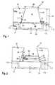
- FIG. 1shows the fabrication of an SiO 2 structure with an overhang structure (reentrant), i.e. with the structure tapering toward the top,
- FIG. 2shows the deposition of a lower metal contact of a tunnel element and of an oxidizing layer, e.g. an aluminum layer,
- FIG. 3shows the anodic oxidation of the aluminum layer for fabrication of a tunnel barrier
- FIG. 4shows the application of an upper metal contact of the tunnel element
- FIG. 5shows the application of a sealing layer, for example of SiO 2 ,
- FIG. 6shows the sealing level after a leveling process
- FIG. 7shows a structure in accordance with an exemplary embodiment comprising organic materials
- FIG. 8shows the structure after an organic mask layer has been dissolved off
- FIG. 9shows the application of an encapsulation layer
- FIG. 10shows the structure with leveled encapsulation layer.
- FIG. 1shows the fabrication of a structure 10 which is, for example, trapezoid-shaped in cross section, on a substrate layer 12 comprising, for example, silicon dioxide.
- a conductor-track contactfor example comprising copper, has been embedded in the substrate layer 12 in a preceding method step. This conductor track is embedded, for example, using the damascene technique.
- a barrier layerwhich is approximately 5 nm (nanometers) thick and consists, for example, of tantalum nitride.
- a mask layer 16 of, for example, silicon dioxideis applied to the substrate layer 12 and the conductor-track contact 14 .
- the thickness D1 of the mask layer 16is greater than the height of a tunnel contact element which is to be fabricated.
- the mask layer 16is structured with the aid of a dry etching process, for example a reactive ion etching process, in order, for example, to produce the structure 10 with a trapezoid-shaped cross section.
- a structure of this typeis also known as a reentrant structure.
- a free space 18is formed, the side walls 20 and 22 of which are inclined by an angle ⁇ of >3°, for example of approximately 15°, with respect to the normal n to the substrate layer 12 and/or the conductor-track contact 14 .
- the opening of the free space 18has a width B1 of, for example, 180 nm.
- the free space 18widens toward the conductor-track contact 14 and, at the conductor-track 14 , has a width B2 which is greater than the width B1, e.g. 200 nm.
- the mask layer 16remains in place in the edge regions of the conductor-track contact 14 and overlaps the conductor-track contact 14 by an overlap distance S of, for example 20 nm.
- the etchingends when the surface of the conductor-track contact 14 is reached.
- the opening of the free space 18 and its basic surface areaare, for example, square, rectangular or oval.
- FIG. 2shows the deposition of a lower contact stack 50 of the tunnel element which is to be fabricated.
- the depositiontakes place electrochemically using external current, i.e. by electrodeposition.
- a positive potentialis applied to the barrier layer 24 , which extends as far as the edge regions of the silicon wafers and on which the structure 10 is situated.
- the mask layer 16has a high impedance and therefore acts as an electrical insulator.
- the conductor-track contact 14has a very good conductivity and therefore acts as an anode during the deposition.
- a metal layer 52 of copperis deposited in a uniform thickness on the conductor-track contact 14 .
- a Permalloy layer 54is electrodeposited on the copper layer 52 .
- a cobalt-iron layer 56is electrodeposited on the Permalloy layer 54 .
- the cobalt-iron layer 56also has a uniform thickness.
- the thicknesses of the copper layer 52 , the Permalloy layer 54 and the cobalt-iron layer 56are, in this order, for example 3 nm, 4 nm and 1 nm.
- an aluminum layer 58 with a uniform thickness of, for example, 1.5 nmis electrodeposited on the cobalt-iron layer 56 .
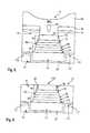
- FIG. 3shows the anodic oxidation of the aluminum layer 58 to form an aluminum oxide layer 60 .
- the oxygenwhich arrives at the anode oxidizes the aluminum layer 58 uniformly to produce the aluminum oxide layer 60 .
- the aluminum oxide layer 60has a thickness of, for example, 2 nm.
- the aluminum oxide layer 60forms the tunnel barrier of the tunnel contact element which is to be fabricated.
- the aluminum layer 58is not completely oxidized all the way through, but rather is only partially oxidized. By way of example, one to three atomic layers of the aluminum layer 58 are retained beneath the aluminum oxide layer 60 .
- FIG. 4shows the application of an upper metal stack 70 of the tunnel element which is to be fabricated.
- a cobalt-iron layer 72which is, for example, about 2 nm thick is applied to the aluminum oxide layer 60 .
- a space Z1is formed at the edge of the cobalt-iron layer 72 , between this layer and the mask layer 16 .
- a cobalt-iron layer 74is applied to the mask layer 16 .
- an iron-manganese layer 76is applied to the cobalt-iron layer 72 .
- the area occupied by the iron-manganese layer 76is, furthermore, smaller than the area occupied by the cobalt-iron layer 72 .
- a space Z2is formed between iron-manganese layer 76 and the mask layer 16 .
- an iron-manganese layer 78is deposited on the cobalt-iron layer 74 during the application.
- a diffusion barrier of tantalum nitrideis also applied, for example in order to prevent diffusion of copper which is subsequently to be applied.
- This barrier layeris not shown in FIG. 4.
- FIG. 5shows the application of a sealing layer 90 , for example of silicon dioxide, to the structure 10 .
- the thickness of the sealing layer 90is selected in such a way that, in a subsequent polishing operation, the polishing can be stopped at the iron-manganese layer 76 or at the barrier layer which has been applied thereto.
- a cavity 92is located above the level at which the polishing operation is stopped and therefore causes no further disruption.
- the sealing layer 90penetrates into the remaining free space, all the way to the aluminum oxide layer 60 , and fills the remaining free spaces and intermediate spaces with silicon dioxide.
- the cobalt-iron layer 72 and the iron-manganese layer 76are completely encapsulated.
- the sealing layeraccumulates above the iron-manganese layer 78 .
- FIG. 6shows the level sealing layer 90 .
- Levelingis carried out with the aid of a chemical-mechanical polishing process.
- the polishing processis ended at the surface of the iron-manganese layer 76 or at the surface of the barrier layer which has been applied thereto.
- the cobalt-iron layer 74which has been applied to the mask layer 16 and the iron-manganese layer 78 above the cobalt-iron layer 74 are removed.
- the structure 10then only includes parts of the sealing layer 90 which lie to the sides of the cobalt-iron layer 72 and of the iron-manganese layer 76 .
- the fabrication of the upper conductor-track contactcan be commenced.
- the fabrication processwhich has been explained with reference to FIGS. 1 to 6 leads to the formation of a tunnel contact element 100 , the layers of which are of uniform thickness.
- the aluminum oxide layer 60is not electrically short-circuited by materials of the cobalt-iron layer 72 or of the iron-manganese layer 76 above it.
- the barrier layer 24can be separated again from the surface of the structure 10 .
- side walls made from the material of the mask layer 16remain in place around the tunnel contact element 100 .
- the substrate layer 12is fabricated, for example, from an organic and electrically nonconductive material.
- the organic substrate layeris closed off by an additional hard mask layer 110 which consists, for example, of SiON, SiO 2 or Si 3 N 4 .
- the boundary between the mask layer 110 and the organic substrate layeris indicated by dashed lines 112 in FIGS. 1 to 6 . Otherwise, the method steps and materials explained with reference to FIGS. 1 to 6 remain identical.
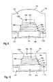
- FIG. 7shows a structure 10 b in accordance with an exemplary embodiment in which, instead of the substrate layer 12 , a substrate layer 120 comprising, for example, an organic material is used. Above the substrate layer 120 there is, for example, a hard mask layer 110 b . In the exemplary embodiment illustrated in FIG. 7 too, a barrier layer 24 b between substrate layer 120 and conductor-track contact 14 b is used to avoid diffusion of the copper of the conductor-track contact 14 b into the substrate layer 120 . A mask layer 122 comprising an organic material has been applied to the barrier layer 24 b and the conductor-track contact 14 b. Otherwise, the same method steps as those which have been explained above with reference to FIGS.
- a contact stack 50 bwhich includes the layers 52 b , 54 b and 56 b,
- a metal stack 70 bwhich includes the layers 72 b and 76 b,
- the mask layer 122is dissolved off in a following process step. Spaces 124 and 126 between the cobalt-iron layer 72 b and the mask layer 122 and between the iron-manganese layer 76 b and the mask layer 122 make it easier for a solvent to penetrate and therefore dissolve the mask layer 122 .
- the layers 74 b and 78 b which lie on the mask layer 122are also dissolved away together with the mask layer 122 .
- FIG. 8shows the structure 10 b after the dissolution process.
- This processis also known as the lift-off process.
- the combination of two coating methods, namely electrochemical deposition and sputtering, the use of anodic oxidation for fabrication of the tunnel barrier 60 b and the use of the lift-off processprevents electrical short-circuits across the aluminum oxide layer 60 b .
- the barrier layer 24 b above the hard mask layer 24 bis exposed again.
- the side faces of the tunnel contact element 100 bare also exposed during the dissolution.
- FIG. 9shows an encapsulation layer 150 of, for example, an organic material which has been applied to the structure 10 b .
- the encapsulation layer 150is applied in a thickness which is greater than the height of the tunnel contact element 100 b .
- a projection 152forms above the tunnel contact element 100 b .
- the encapsulation layer 150is leveled in a following process step, for example by means of a chemical-mechanical polishing process.
- FIG. 10shows the structure 10 b at the end of the polishing process.
- the polishing processwas stopped at the upper face of the iron-manganese layer 76 b . This substantially concludes the fabrication of the tunnel contact element 10 b .
- an upper conductor-track contact and further componentsare applied (not shown).
- a diffusion barrier which is sputtered on prior to the removal of the mask layer 122 by dissolutioncan also be used as a stop layer for the polishing process for leveling the encapsulation layer 150 .
- an inorganic materialfor example silicon dioxide, is used for the substrate layer 120 .
- the mask layer 122consists of an organic material.
- the encapsulation layercomprises an organic material.
- the encapsulation layer 150consists of an inorganic material, such as for example silicon dioxide.
- An organic materialis once again used for the mask layer 122 .
- the encapsulation layercomprises an inorganic material.
Landscapes
- Engineering & Computer Science (AREA)
- Manufacturing & Machinery (AREA)
- Internal Circuitry In Semiconductor Integrated Circuit Devices (AREA)
- Semiconductor Memories (AREA)
- Electrodes Of Semiconductors (AREA)
Abstract
Description
- The invention relates to a method in which an electrically conductive contact layer is supported by a substrate layer, for example by a silicon wafer. An electrically nonconductive mask layer, for example a photoresist, is applied to the electrically conductive contact layer. Then, part of the mask layer is removed, in order for at least one electrically conductive layer subsequently to be applied to the contact layer in the free space which is formed.[0001]
- Approximately the following conductivities κ can be given for nonconductive layers, i.e. for insulator layers, for semiconductor layers and for electrically conductive layers:[0002]
- organic and inorganic insulators κ=10[0003]−18to 10−7Ω−1/m−1,
- semiconductors κ=10[0004]−7to 10−4Ω−1/m−1, and
- electrically conductive layers, in particular metal layers, κ>10[0005]4Ω−1/m−1, in particular in the range κ=104to 105Ω−1/m−1.
- Various methods for applying the electrically conductive layers during the fabrication of integrated circuit arrangements are known, including:[0006]
- vapor deposition,[0007]
- sputtering, and[0008]
- electrochemical deposition.[0009]
- When using vapor deposition and sputtering, layers which, firstly, may have an uneven thickness above the silicon wafer are deposited over the entire silicon wafer. Secondly, layer sections within free spaces of the mask layer have different thicknesses, in particular in the vicinity of steps. These drawbacks cause problems for many applications. Vapor deposition and sputtering are possible both for the application of electrically conductive layers and for the application of electrically nonconductive layers.[0010]
- Electrochemical coating methods can be used to deposit layers with a very uniform layer thickness. A distinction is drawn between electrodeposition and deposition which does not use external current. In the case of the electrodeposition of metal, electrons are supplied by an external current source. A z-times positively charged metal ion is reduced by taking up z electrons, z being an integer greater than 0. No external current source is required for the deposition of metals without using external current. The electrons required for the reduction originate from a reducing agent which is contained in an electrolyte solution. Electrochemical deposition is only possible for electrically conductive layers.[0011]
- It is an object of the invention to describe simple methods for the fabrication of an integrated circuit arrangement with electrically conductive and electrically nonconductive layers. In addition, it is intended to provide associated integrated circuit arrangements and a tunnel contact element.[0012]
- The object relating to the method is achieved by the method steps described in patent claim 1. Refinements are given in the subclaims.[0013]
- In the method according to the invention, in addition to the method steps described in the introduction, at least one electrically conductive layer is electrochemically deposited in the free space, which is formed during the removal of parts of the mask layer, by means of electrochemical deposition.[0014]
- During the electrochemical deposition, no materials are precipitated on the electrically nonconductive mask layer.[0015]
- This eliminates the need for steps which would be required in order to remove such materials. The use of an electrochemical coating method means that layers of uniform thickness are formed within the free space. Moreover, the layers can be very thin, for example less than 2 nm thick. The thickness of the layers is uniform both within the free space and at different locations on a silicon wafer with a diameter of, for example, 200 or 300 mm. Electrochemical coating is a very inexpensive coating method compared to vapor deposition or sputtering. Consequently, the lower part of the layer system can be produced with relatively little outlay. For the fabrication of very thin layers, the yield during the fabrication of integrated circuit arrangements rises considerably, since the thickness of the layers which are deposited can be set relatively accurately in technological terms.[0016]
- Moreover, in the method according to the invention, after the electrochemical deposition an electrically nonconductive layer is introduced into the free space. Consequently, electrochemical deposition of further layers is no longer possible. One further layer or a plurality of further layers are introduced into the free space using other coating techniques. The further layer or layers may be electrically conductive, electrically nonconductive or semiconducting. During the application of the further layer or layers, layers of the same materials are formed outside the free space. These layers are removed in a removal process.[0017]
- Therefore, the component which is to be fabricated is already present in the free space even before the removal process. Measures for laterally delimiting the applied layers, as are often required with conventional coating methods, are no longer necessary. Such measures would lead to mixing of materials at the side edges. In unfavorable situations, this mixing of materials would lead to the electrically nonconductive layer being bridged by electrically conductive material, thus leading to an electrical short circuit. However, the method according to the invention avoids just such a bridging effect. Consequently, it is possible to produce components with a high yield.[0018]
- In the method according to the invention, the layer deposited last is completely or partially oxidized to form an electrically nonconductive layer in an oxidation operation which is preferably carried out anodically. The result of this measure is that the nonconductive layer can be fabricated from a conductive layer. During the oxidation, the thickness of the layer only changes to an insignificant extent, and does so uniformly. Consequently, the thickness of the nonconductive layer is uniform. Alternatively, an electrically nonconductive layer is applied, for example by sputtering or vapor deposition, to the layer which was deposited last. In this alternative, a uniform foundation for the nonconductive layer which is applied is produced by the deposition of the preceding layers. This also leads to a more uniform nonconductive layer. In many applications, the nonconductive layer is the layer which is critical for fabrication, e.g. the thinnest layer. The use of the method according to the invention allows the nonconductive layer to be applied with lower tolerances. This also increases the yield during the fabrication of the integrated circuit arrangement.[0019]
- If electrodeposition, i.e. with external current, is used, the electrically conductive contact layer and/or the electrically conductive layers which have been deposited above it form the anode. When using certain materials for the electrically conductive contact layer, for example in the case of copper or highly doped semiconductors, what are known as diffusion barriers and/or adhesion layers are used, referred to below as interlayers. The interlayer consists, for example, of TaN (tantalum nitride). The interlayer can also be used as an anode for electrodeposition. If the interlayer extends as far as the edge region of the processed silicon wafer, external current can easily be supplied via the edges of the silicon wafer. Direct current or alternating current can be used for the electrodeposition.[0020]
- In one refinement, the mask layer overlaps the electrically conductive layer on all sides. In the refinement, at least two electrically conductive layers of different materials are deposited in succession. The overlapping on all sides ensures that only the first material reaches the electrically conductive contact layer. The first layer is then deposited with a uniform thickness. During deposition of the second layer, material from this layer no longer reaches the electrically conductive contact layer. The second electrically conductive layer is deposited in a uniform thickness above the layer applied previously. The edge regions of the layers also have the same thickness as the remainder of the layer. There is no curvature in the edge regions caused by a different layer thickness.[0021]
- As has already been mentioned, the thickness of the mask layer is dimensioned in such a way that the further layer lies below the opening of the free space. In a refinement, a removal process in a subsequent method step is used to remove regions which lie outside the free space and have formed during the application of the further layer. Consequently, these regions no longer impede the further fabrication of the integrated circuit arrangement. By way of example, a chemical-mechanical polishing (CMP) process is used for the removal. It is also possible to remove part of the mask layer. The remainder of the mask layer remains on the substrate layer and delimits the layer system within the free space on all sides.[0022]
- In a further refinement, a sealing layer is applied prior to the polishing process, occupying the as yet unfilled space of the free space. During the polishing process, the sealing layer is removed down to the height of the layer which was applied last. The result of the sealing is that during subsequent method steps no material enters the space between the further layers and the mask layer. Such material would change the electrical properties of the layer system.[0023]
- In an alternative refinement, the mask layer is completely removed during the removal process, for example by what is known as a lift-off process. As a result, the layers which form outside the free space during the application of the further layer are also removed and do not disrupt the further method steps.[0024]
- In one refinement of the alternative, the mask layer consists of an organic material. The mask layer is dissolved off with the aid of a suitable solvent. All organic materials which can be used in semiconductor technology are suitable materials for the mask layer. The trend is toward organic materials with low dielectric constants. Examples of materials of this type are polyimides, which if appropriate may be mixed with fluorine. Moreover, spin-on glass materials, i.e. glass materials which are applied to the substrate layer using the spinning method, are also used. Other possibilities are alkylsilanes, ultra low-k materials, such as for example Teflon, porous dielectrics, such as for example aerogels, or also SiLK, a hydrocarbon compound which does not contain any silicon.[0025]
- In one configuration, an encapsulation layer is applied after the removal of the mask layer. The encapsulation layer is removed down to the height of the layer which was applied last, preferably using a chemical-mechanical polishing process. The encapsulation layer is used to encapsulate the layer system, so that no substances disrupt the layer system during the further method steps.[0026]
- In another refinement, parts of the mask layer are removed, for example by anisotropic etching, in such a way that the free space widens toward the substrate layer, preferably on all sides. The structure which forms is also known as a reentrant structure. The inclination of the walls of the free space, i.e. the overhang is, for example, more than 5 percent with respect to the normal to the substrate layer. By way of example, inclination angles of 5 percent, 10 percent or 20 percent are used. The inclination causes the mask layer to act as what is known as a shadow mask during the application of the further layers. When sputtering the further layers, excessively strong flattened sections in the edge regions of the layer to be applied are prevented by the shadow mask. However, it is also possible to work without inclined side walls.[0027]
- In a further refinement, the free space is, for example, trapezoid-shaped in cross section. The side walls of the free space along a cross section through the mask layer form, for example, straight lines. This makes it considerably easier to fabricate the free space. However, free spaces which widen toward the substrate layer only in the region of the further layers and then have approximately uniform diameters are also employed.[0028]
- In another refinement, the mask layer has a planar surface and includes a multiplicity of recesses in which components of a similar type are arranged. The contact layers of a plurality of components are connected to one another, for example in the form of a matrix in rows and columns. This measure makes it easy to feed current to the interconnected contact layers during the electrodeposition. This facilitates the electrodeposition operation even for a very large number of components, for example several hundreds of thousands of components on an integrated circuit arrangement. A plurality of integrated circuit arrangements are fabricated on one silicon wafer with a diameter of 200 mm, 300 mm or above. In the case of integrated circuits, the combination of electrochemical deposition and other coating techniques can be used, and is in many respects superior to the method for the fabrication of an integrated circuit arrangement which has hitherto been employed.[0029]
- In one refinement, the mask layer is thinner than 100 nm, preferably thinner than 50 nm. At least one layer which is introduced into the cavity is thinner than 5 nm. Particularly with layer thicknesses of this level, the use of the method according to the invention or its refinements result in the fabrication of significantly more homogeneous and more uniform layers than those achieved with other methods. Said layer thicknesses are required, for example, for the fabrication of tunnel contact elements, i.e. for contact elements which exploit what is known as the tunnel effect of electrons through insulators.[0030]
- Therefore, in another refinement, at least one electrically nonconductive layer which is introduced into the free space is fabricated with a thickness which is such that electrons can only cross through the layer using the tunnel effect.[0031]
- In one configuration, an electrically conductive layer is introduced into the free space by electrochemical deposition. Then, this layer is oxidized to form an electrically nonconductive layer, preferably by anodic oxidation. This technology can be used in particular for tunnel elements to achieve a high yield during production. This is because sputtering of very thin layers causes problems. Compared to other oxidation methods, anodic oxidation has advantages in terms of the oxidation time and the uniformity of oxidation.[0032]
- In a further refinement, the following materials are used:[0033]
- a quartz glass or an organic, electrically nonconductive material for the mask layer and/or the sealing layer,[0034]
- aluminum, for example, for the layer deposited last, and/or[0035]
- hard magnetic materials and/or layers of soft magnetic material for further layers which are deposited in the free space or are applied in the free space.[0036]
- The use of hard magnetic and soft magnetic layers makes it possible to fabricate magnetic memory elements which make use of the tunnel effect. Memories of this type are known as Magnetic Random Access Memories (MRAMs). Hard magnetic materials which are used are:[0037]
- ferromagnets, such as for example FeMn, NiMn, IrMn and PtMn,[0038]
- pseudo-spin valves, such as for example SrPdMn, or[0039]
- artificial antiferromagnets, such as for example Co/Cu/Co, Fe/Cr/Fe, CoFe/Ru/CoFe.[0040]
- A common feature of these materials is that a magnetic field with a field strength of, for example, more than 100 Oersted are required in order to change the orientation of the magnetization within the materials.[0041]
- The soft magnetic material used is, for example, a layer of FeNi or CoPt. Combinations of the hard magnetic and/or the soft magnetic layers are also used.[0042]
- The invention also relates to a circuit arrangement in which at least one layer of a layer system has been fabricated by electrochemical deposition. The mask layer is older than the layer produced by electrochemical deposition. The mask layer therefore has a dual function. It is used as protection for encapsulation of the layer system and forms a lateral boundary during the electrochemical deposition. Consequently, the technical effects referred to above also apply to the circuit arrangement.[0043]
- Moreover, the invention relates to a circuit arrangement in which an encapsulation layer encloses a layer system which includes at least one layer deposited by electrochemical deposition. The encapsulation layer is newer than the deposited layer. The technical effects described above also apply to the circuit arrangement, in particular the effects described in connection with the mask layer and its removal.[0044]
- In addition to the layer deposited by electrochemical deposition or in addition to the layers deposited by electrochemical deposition, in a refinement of the circuit arrangement with encapsulation layer, the layer system includes at least one electrically nonconductive layer, above which further layers are arranged.[0045]
- Moreover, in a refinement of the circuit arrangement with encapsulation layer, at least one layer of the layer system has a larger basic surface area than a layer which lies between this layer and the contact layer. The widening of the layer surface areas towards the contact layer is attributable to the inclined side walls of a mask layer which has already been removed. Consequently, the technical effects described above also apply to the circuit arrangement.[0046]
- In refinements of the circuit arrangements, the circuit arrangements have features which also arise in circuit arrangements which have been produced using the method according to the invention or one of its refinements. For example, a sealing layer is used, the side walls of the mask layer are inclined, the materials listed above are employed and/or the layer thicknesses given above are used. The technical effect referred to above correspondingly slide to the refinements.[0047]
- Furthermore, the invention relates to a tunnel contact element which includes at least two electrically conductive contact layers. Between the contact layers there is an electrically nonconductive barrier layer, the thickness of which is such that electrons can only cross through it using the tunnel effect. The barrier layer and/or a contact layer have been fabricated by electrochemical deposition. This measure allows the layer in question to be fabricated with a high degree of accuracy and a uniform thickness. The yield of tunnel element fabrication is very high.[0048]
- In a further refinement, the barrier layer is fabricated by anodic oxidation. In this case, one of the electrically conductive contact layers is used as electrode for electrodeposition.[0049]
- In a refinement, the tunnel contact element has features which also occur in a circuit arrangement which has been fabricated using the method according to the invention or one of its refinements. The features and technical effects described above therefore also apply to the tunnel contact element.[0050]
- Exemplary embodiments of the invention are explained below with reference to the appended drawings, in which:[0051]
- FIG. 1 shows the fabrication of an SiO[0052]2structure with an overhang structure (reentrant), i.e. with the structure tapering toward the top,
- FIG. 2 shows the deposition of a lower metal contact of a tunnel element and of an oxidizing layer, e.g. an aluminum layer,[0053]
- FIG. 3 shows the anodic oxidation of the aluminum layer for fabrication of a tunnel barrier,[0054]
- FIG. 4 shows the application of an upper metal contact of the tunnel element,[0055]
- FIG. 5 shows the application of a sealing layer, for example of SiO[0056]2,
- FIG. 6 shows the sealing level after a leveling process,[0057]
- FIG. 7 shows a structure in accordance with an exemplary embodiment comprising organic materials,[0058]
- FIG. 8 shows the structure after an organic mask layer has been dissolved off,[0059]
- FIG. 9 shows the application of an encapsulation layer, and[0060]
- FIG. 10 shows the structure with leveled encapsulation layer.[0061]
- FIG. 1 shows the fabrication of a[0062]
structure 10 which is, for example, trapezoid-shaped in cross section, on asubstrate layer 12 comprising, for example, silicon dioxide. A conductor-track contact, for example comprising copper, has been embedded in thesubstrate layer 12 in a preceding method step. This conductor track is embedded, for example, using the damascene technique. Betweensubstrate layer 12 and conductor-track contact 14 there is a barrier layer which is approximately 5 nm (nanometers) thick and consists, for example, of tantalum nitride. Amask layer 16 of, for example, silicon dioxide is applied to thesubstrate layer 12 and the conductor-track contact 14. The thickness D1 of themask layer 16 is greater than the height of a tunnel contact element which is to be fabricated. - Then, the[0063]
mask layer 16 is structured with the aid of a dry etching process, for example a reactive ion etching process, in order, for example, to produce thestructure 10 with a trapezoid-shaped cross section. A structure of this type is also known as a reentrant structure. During the etching process, afree space 18 is formed, theside walls substrate layer 12 and/or the conductor-track contact 14. Along the cross section illustrated in FIG. 1, the opening of thefree space 18 has a width B1 of, for example, 180 nm. Thefree space 18 widens toward the conductor-track contact 14 and, at the conductor-track 14, has a width B2 which is greater than the width B1, e.g. 200 nm. Themask layer 16 remains in place in the edge regions of the conductor-track contact 14 and overlaps the conductor-track contact 14 by an overlap distance S of, for example 20 nm. The etching ends when the surface of the conductor-track contact 14 is reached. The opening of thefree space 18 and its basic surface area are, for example, square, rectangular or oval. - FIG. 2 shows the deposition of a[0064]
lower contact stack 50 of the tunnel element which is to be fabricated. The deposition takes place electrochemically using external current, i.e. by electrodeposition. In this case, a positive potential is applied to thebarrier layer 24, which extends as far as the edge regions of the silicon wafers and on which thestructure 10 is situated. Themask layer 16 has a high impedance and therefore acts as an electrical insulator. The conductor-track contact 14 has a very good conductivity and therefore acts as an anode during the deposition. First of all, ametal layer 52 of copper is deposited in a uniform thickness on the conductor-track contact 14. - Then, in a second deposition process, by way of example a[0065]
Permalloy layer 54 is electrodeposited on thecopper layer 52. In a subsequent deposition process, by way of example a cobalt-iron layer 56 is electrodeposited on thePermalloy layer 54. The cobalt-iron layer 56 also has a uniform thickness. The thicknesses of thecopper layer 52, thePermalloy layer 54 and the cobalt-iron layer 56 are, in this order, for example 3 nm, 4 nm and 1 nm. - In a subsequent method step, an[0066]
aluminum layer 58 with a uniform thickness of, for example, 1.5 nm is electrodeposited on the cobalt-iron layer 56. - FIG. 3 shows the anodic oxidation of the[0067]
aluminum layer 58 to form analuminum oxide layer 60. The oxygen which arrives at the anode oxidizes thealuminum layer 58 uniformly to produce thealuminum oxide layer 60. At the end of the oxidation operation, thealuminum oxide layer 60 has a thickness of, for example, 2 nm. Thealuminum oxide layer 60 forms the tunnel barrier of the tunnel contact element which is to be fabricated. - In another exemplary embodiment, the[0068]
aluminum layer 58 is not completely oxidized all the way through, but rather is only partially oxidized. By way of example, one to three atomic layers of thealuminum layer 58 are retained beneath thealuminum oxide layer 60. - FIG. 4 shows the application of an[0069]
upper metal stack 70 of the tunnel element which is to be fabricated. In a first process step, for example in a sputtering process, a cobalt-iron layer 72 which is, for example, about 2 nm thick is applied to thealuminum oxide layer 60. Moreover, a space Z1 is formed at the edge of the cobalt-iron layer 72, between this layer and themask layer 16. Moreover, a cobalt-iron layer 74 is applied to themask layer 16. - In a subsequent process step, by way of example an iron-[0070]
manganese layer 76 is applied to the cobalt-iron layer 72. The area occupied by the iron-manganese layer 76 is, furthermore, smaller than the area occupied by the cobalt-iron layer 72. A space Z2 is formed between iron-manganese layer 76 and themask layer 16. Moreover, an iron-manganese layer 78 is deposited on the cobalt-iron layer 74 during the application. - Then, in the exemplary embodiment, a diffusion barrier of tantalum nitride is also applied, for example in order to prevent diffusion of copper which is subsequently to be applied. This barrier layer is not shown in FIG. 4.[0071]
- FIG. 5 shows the application of a[0072]
sealing layer 90, for example of silicon dioxide, to thestructure 10. The thickness of thesealing layer 90 is selected in such a way that, in a subsequent polishing operation, the polishing can be stopped at the iron-manganese layer 76 or at the barrier layer which has been applied thereto. Acavity 92 is located above the level at which the polishing operation is stopped and therefore causes no further disruption. Thesealing layer 90 penetrates into the remaining free space, all the way to thealuminum oxide layer 60, and fills the remaining free spaces and intermediate spaces with silicon dioxide. As a result, the cobalt-iron layer 72 and the iron-manganese layer 76 are completely encapsulated. Moreover, the sealing layer accumulates above the iron-manganese layer 78. - FIG. 6 shows the[0073]
level sealing layer 90. Leveling is carried out with the aid of a chemical-mechanical polishing process. The polishing process is ended at the surface of the iron-manganese layer 76 or at the surface of the barrier layer which has been applied thereto. During the polishing operation, the cobalt-iron layer 74 which has been applied to themask layer 16 and the iron-manganese layer 78 above the cobalt-iron layer 74 are removed. After the polishing operation, thestructure 10 then only includes parts of thesealing layer 90 which lie to the sides of the cobalt-iron layer 72 and of the iron-manganese layer 76. After the polishing operation, the fabrication of the upper conductor-track contact can be commenced. The fabrication process which has been explained with reference to FIGS.1 to6 leads to the formation of atunnel contact element 100, the layers of which are of uniform thickness. In particular, thealuminum oxide layer 60 is not electrically short-circuited by materials of the cobalt-iron layer 72 or of the iron-manganese layer 76 above it. - In further method steps, the[0074]
barrier layer 24 can be separated again from the surface of thestructure 10. In the process, side walls made from the material of themask layer 16 remain in place around thetunnel contact element 100. - In another exemplary embodiment, the[0075]
substrate layer 12 is fabricated, for example, from an organic and electrically nonconductive material. In this case, the organic substrate layer is closed off by an additionalhard mask layer 110 which consists, for example, of SiON, SiO2or Si3N4. The boundary between themask layer 110 and the organic substrate layer is indicated by dashedlines 112 in FIGS.1 to6. Otherwise, the method steps and materials explained with reference to FIGS.1 to6 remain identical. - FIG. 7 shows a[0076]
structure 10bin accordance with an exemplary embodiment in which, instead of thesubstrate layer 12, asubstrate layer 120 comprising, for example, an organic material is used. Above thesubstrate layer 120 there is, for example, ahard mask layer 110b. In the exemplary embodiment illustrated in FIG. 7 too, abarrier layer 24bbetweensubstrate layer 120 and conductor-track contact 14bis used to avoid diffusion of the copper of the conductor-track contact 14binto thesubstrate layer 120. Amask layer 122 comprising an organic material has been applied to thebarrier layer 24band the conductor-track contact 14b.Otherwise, the same method steps as those which have been explained above with reference to FIGS.1 to6 for the fabrication of thestructure 10 were carried out for fabrication of thestructure 10b. Layers of the same material, with the same dimensions and the same function therefore bear the same reference numeral in FIG. 7, but with the added suffix of a lower-case letter b. This applies to the following layers: - a[0077]
copper layer 52b, - a[0078]
Permalloy layer 54b, - a cobalt-[0079]
iron layer 56b, - a[0080]
contact stack 50bwhich includes thelayers - an[0081]
aluminum oxide layer 60b, - a cobalt-[0082]
iron layer 72bapplied to the aluminum oxide layer, - an iron-[0083]
manganese layer 76b, - a[0084]
metal stack 70bwhich includes thelayers - a cobalt-[0085]
iron layer 74bwhich has been applied to themask layer 122, and - an iron-manganese layer[0086]78i b above the cobalt-
iron layer 74b. - [0087]
Side walls side walls side walls structure 10b, for example with respect to the conductor-track contact 14b, as theside walls structure 10 with respect to the conductor-track contact 14. Afree space 18bcorresponds to thefree space 18. - After the process steps involved in the fabrication of the[0088]
structure 10billustrated in FIG. 7, themask layer 122 is dissolved off in a following process step.Spaces iron layer 72band themask layer 122 and between the iron-manganese layer 76band themask layer 122 make it easier for a solvent to penetrate and therefore dissolve themask layer 122. Thelayers mask layer 122 are also dissolved away together with themask layer 122. - FIG. 8 shows the[0089]
structure 10bafter the dissolution process. This process is also known as the lift-off process. The combination of two coating methods, namely electrochemical deposition and sputtering, the use of anodic oxidation for fabrication of thetunnel barrier 60band the use of the lift-off process prevents electrical short-circuits across thealuminum oxide layer 60b. After themask layer 122 has been dissolved away, thebarrier layer 24babove thehard mask layer 24bis exposed again. The side faces of thetunnel contact element 100bare also exposed during the dissolution. - FIG. 9 shows an[0090]
encapsulation layer 150 of, for example, an organic material which has been applied to thestructure 10b. Theencapsulation layer 150 is applied in a thickness which is greater than the height of thetunnel contact element 100b. Aprojection 152 forms above thetunnel contact element 100b. Theencapsulation layer 150 is leveled in a following process step, for example by means of a chemical-mechanical polishing process. - FIG. 10 shows the[0091]
structure 10bat the end of the polishing process. The polishing process was stopped at the upper face of the iron-manganese layer 76b. This substantially concludes the fabrication of thetunnel contact element 10b. In further method steps, by way of example, an upper conductor-track contact and further components are applied (not shown). - A diffusion barrier which is sputtered on prior to the removal of the[0092]
mask layer 122 by dissolution can also be used as a stop layer for the polishing process for leveling theencapsulation layer 150. - In another exemplary embodiment, an inorganic material, for example silicon dioxide, is used for the[0093]
substrate layer 120. In this case, there is no need for ahard mask layer 110b. In this exemplary embodiment, themask layer 122 consists of an organic material. The encapsulation layer comprises an organic material. - In a further exemplary embodiment, the[0094]
encapsulation layer 150 consists of an inorganic material, such as for example silicon dioxide. An organic material is once again used for themask layer 122. The encapsulation layer comprises an inorganic material.
Claims (21)
Applications Claiming Priority (2)
| Application Number | Priority Date | Filing Date | Title |
|---|---|---|---|
| DE10048420ADE10048420A1 (en) | 2000-09-29 | 2000-09-29 | Method for producing integrated circuit arrangements and associated circuit arrangements, in particular tunnel contact elements |
| DE10048420.4 | 2000-09-29 |
Publications (2)
| Publication Number | Publication Date |
|---|---|
| US20020076572A1true US20020076572A1 (en) | 2002-06-20 |
| US6864175B2 US6864175B2 (en) | 2005-03-08 |
Family
ID=7658171
Family Applications (1)
| Application Number | Title | Priority Date | Filing Date |
|---|---|---|---|
| US09/957,363Expired - Fee RelatedUS6864175B2 (en) | 2000-09-29 | 2001-09-20 | Method for fabricating integrated circuit arrangements, and associated circuit arrangements, in particular tunnel contact elements |
Country Status (4)
| Country | Link |
|---|---|
| US (1) | US6864175B2 (en) |
| EP (1) | EP1193742A3 (en) |
| DE (1) | DE10048420A1 (en) |
| TW (1) | TW508674B (en) |
Cited By (6)
| Publication number | Priority date | Publication date | Assignee | Title |
|---|---|---|---|---|
| US6677165B1 (en)* | 2003-03-20 | 2004-01-13 | Micron Technology, Inc. | Magnetoresistive random access memory (MRAM) cell patterning |
| US20050079638A1 (en)* | 2003-10-14 | 2005-04-14 | Drewes Joel A. | System and method for reducing shorting in memory cells |
| US20050136648A1 (en)* | 2003-12-23 | 2005-06-23 | Mariah Sharma | Method and system for forming a contact in a thin-film device |
| US20070279971A1 (en)* | 2004-06-04 | 2007-12-06 | Micron Technology, Inc. | Modified pseudo-spin valve (psv) for memory applications |
| US20130069067A1 (en)* | 2011-09-20 | 2013-03-21 | Keun Chun Youn | Organic light emitting diode (oled) display device and method for manufacturing the same |
| JP2017084916A (en)* | 2015-10-27 | 2017-05-18 | 株式会社日立ハイテクノロジーズ | Device manufacturing method and plasma processing method |
Families Citing this family (4)
| Publication number | Priority date | Publication date | Assignee | Title |
|---|---|---|---|---|
| US6974708B2 (en)* | 2004-04-08 | 2005-12-13 | Headway Technologies, Inc. | Oxidation structure/method to fabricate a high-performance magnetic tunneling junction MRAM |
| DE102005030376B4 (en) | 2005-06-29 | 2009-03-26 | Siemens Ag | Manufacturing method for a contact surface in an electromagnet and electromagnet |
| US8553449B2 (en)* | 2009-01-09 | 2013-10-08 | Micron Technology, Inc. | STT-MRAM cell structures |
| US10651365B2 (en) | 2017-03-16 | 2020-05-12 | Vanguard International Semiconductor Corporation | Electrical contact structure and methods for forming the same |
Citations (3)
| Publication number | Priority date | Publication date | Assignee | Title |
|---|---|---|---|---|
| US20030030948A1 (en)* | 2001-08-13 | 2003-02-13 | Eiji Umetsu | CPP type magnetic sensor or magnetic sensor using tunnel effect, and manufacturing method therefor |
| US6677165B1 (en)* | 2003-03-20 | 2004-01-13 | Micron Technology, Inc. | Magnetoresistive random access memory (MRAM) cell patterning |
| US6744608B1 (en)* | 2002-05-14 | 2004-06-01 | Western Digital (Fremont), Inc. | Method and system for making TMR junctions |
Family Cites Families (9)
| Publication number | Priority date | Publication date | Assignee | Title |
|---|---|---|---|---|
| JPS62103843A (en)* | 1985-10-31 | 1987-05-14 | Pilot Pen Co Ltd:The | perpendicular magnetic recording material |
| US5256565A (en)* | 1989-05-08 | 1993-10-26 | The United States Of America As Represented By The United States Department Of Energy | Electrochemical planarization |
| EP0705474A1 (en)* | 1994-03-25 | 1996-04-10 | Koninklijke Philips Electronics N.V. | Magneto-resistive device, and magnetic head comprising such a device |
| US6590750B2 (en)* | 1996-03-18 | 2003-07-08 | International Business Machines Corporation | Limiting magnetoresistive electrical interaction to a preferred portion of a magnetic region in magnetic devices |
| US5835314A (en)* | 1996-04-17 | 1998-11-10 | Massachusetts Institute Of Technology | Tunnel junction device for storage and switching of signals |
| US5966012A (en)* | 1997-10-07 | 1999-10-12 | International Business Machines Corporation | Magnetic tunnel junction device with improved fixed and free ferromagnetic layers |
| JPH11175920A (en)* | 1997-12-05 | 1999-07-02 | Nec Corp | Magneto-resistance effect type combined head and its manufacture |
| US6177337B1 (en)* | 1998-01-06 | 2001-01-23 | International Business Machines Corporation | Method of reducing metal voids in semiconductor device interconnection |
| US6153443A (en)* | 1998-12-21 | 2000-11-28 | Motorola, Inc. | Method of fabricating a magnetic random access memory |
- 2000
- 2000-09-29DEDE10048420Apatent/DE10048420A1/ennot_activeCeased
- 2001
- 2001-09-07EPEP01121460Apatent/EP1193742A3/ennot_activeWithdrawn
- 2001-09-20USUS09/957,363patent/US6864175B2/ennot_activeExpired - Fee Related
- 2001-09-26TWTW090123721Apatent/TW508674B/ennot_activeIP Right Cessation
Patent Citations (3)
| Publication number | Priority date | Publication date | Assignee | Title |
|---|---|---|---|---|
| US20030030948A1 (en)* | 2001-08-13 | 2003-02-13 | Eiji Umetsu | CPP type magnetic sensor or magnetic sensor using tunnel effect, and manufacturing method therefor |
| US6744608B1 (en)* | 2002-05-14 | 2004-06-01 | Western Digital (Fremont), Inc. | Method and system for making TMR junctions |
| US6677165B1 (en)* | 2003-03-20 | 2004-01-13 | Micron Technology, Inc. | Magnetoresistive random access memory (MRAM) cell patterning |
Cited By (13)
| Publication number | Priority date | Publication date | Assignee | Title |
|---|---|---|---|---|
| US6887719B2 (en)* | 2003-03-20 | 2005-05-03 | Micron Technology, Inc. | Magnetoresistive random access memory (MRAM) cell patterning |
| US20040185675A1 (en)* | 2003-03-20 | 2004-09-23 | Micron Technology, Inc. | Magnetoresistive random access memory (mram) cell patterning |
| US6677165B1 (en)* | 2003-03-20 | 2004-01-13 | Micron Technology, Inc. | Magnetoresistive random access memory (MRAM) cell patterning |
| US7112454B2 (en)* | 2003-10-14 | 2006-09-26 | Micron Technology, Inc. | System and method for reducing shorting in memory cells |
| US20060192235A1 (en)* | 2003-10-14 | 2006-08-31 | Drewes Joel A | System and method for reducing shorting in memory cells |
| US20050079638A1 (en)* | 2003-10-14 | 2005-04-14 | Drewes Joel A. | System and method for reducing shorting in memory cells |
| US20070020775A1 (en)* | 2003-10-14 | 2007-01-25 | Micron Technology, Inc. | System and method for reducing shorting in memory cells |
| US7358553B2 (en) | 2003-10-14 | 2008-04-15 | Micron Technology, Inc. | System and method for reducing shorting in memory cells |
| US7855085B2 (en) | 2003-10-14 | 2010-12-21 | Micron Technology, Inc. | System and method for reducing shorting in memory cells |
| US20050136648A1 (en)* | 2003-12-23 | 2005-06-23 | Mariah Sharma | Method and system for forming a contact in a thin-film device |
| US20070279971A1 (en)* | 2004-06-04 | 2007-12-06 | Micron Technology, Inc. | Modified pseudo-spin valve (psv) for memory applications |
| US20130069067A1 (en)* | 2011-09-20 | 2013-03-21 | Keun Chun Youn | Organic light emitting diode (oled) display device and method for manufacturing the same |
| JP2017084916A (en)* | 2015-10-27 | 2017-05-18 | 株式会社日立ハイテクノロジーズ | Device manufacturing method and plasma processing method |
Also Published As
| Publication number | Publication date |
|---|---|
| EP1193742A3 (en) | 2005-12-28 |
| EP1193742A2 (en) | 2002-04-03 |
| DE10048420A1 (en) | 2002-04-18 |
| TW508674B (en) | 2002-11-01 |
| US6864175B2 (en) | 2005-03-08 |
Similar Documents
| Publication | Publication Date | Title |
|---|---|---|
| US20230238043A1 (en) | Semiconductor structure and method for forming the same | |
| US20220302209A1 (en) | Method of forming memory cell | |
| EP1500116B1 (en) | Method of forming mram devices | |
| US7476329B2 (en) | Methods for contacting conducting layers overlying magnetoelectronic elements of MRAM devices | |
| US7144744B2 (en) | Magnetoresistive random access memory device structures and methods for fabricating the same | |
| US8546151B2 (en) | Method for manufacturing magnetic storage device and magnetic storage device | |
| US10714683B2 (en) | Multilayer hardmask for high performance MRAM devices | |
| US8247905B2 (en) | Formation of vertical devices by electroplating | |
| US20250140295A1 (en) | Method for forming semiconductor device | |
| US6864175B2 (en) | Method for fabricating integrated circuit arrangements, and associated circuit arrangements, in particular tunnel contact elements | |
| US20210249053A1 (en) | Landing pad in interconnect and memory stacks: structure and formation of the same | |
| US12144263B2 (en) | Stepped contact within memory region | |
| US20220367345A1 (en) | Hybrid via interconnect structure | |
| DE112004001003T5 (en) | A method of patterning a lower electrode of a magnetic memory cell prior to deposition of the magnetic stack | |
| US20220352457A1 (en) | Memory device and manufacturing method thereof | |
| US11482666B2 (en) | Method for fabricating a semiconductor device | |
| US6913990B2 (en) | Method of forming isolation dummy fill structures | |
| WO2023093643A1 (en) | Magnetoresistive random-access memory (mram) with preserved underlying dielectric layer | |
| US12219881B2 (en) | Dual layer top contact for magnetic tunnel junction stack | |
| US20250275483A1 (en) | Perpendicular spin-orbit torque magnetic random access memory | |
| US10629650B2 (en) | Integrated circuits with memory cells and methods for producing the same | |
| US20210028349A1 (en) | Integrated circuits with magnetic tunnel junction memory cells and methods for producing the same | |
| US6919234B2 (en) | Method for producing an antifuse in a substrate and an antifuse structure for integration in a substrate |
Legal Events
| Date | Code | Title | Description |
|---|---|---|---|
| FEPP | Fee payment procedure | Free format text:PAYOR NUMBER ASSIGNED (ORIGINAL EVENT CODE: ASPN); ENTITY STATUS OF PATENT OWNER: LARGE ENTITY | |
| AS | Assignment | Owner name:INFINEON TECHNOLOGIES AG, GERMANY Free format text:ASSIGNMENT OF ASSIGNORS INTEREST;ASSIGNORS:ENGELHARDT, MANFRED;WURM, STEFAN;REEL/FRAME:016180/0701;SIGNING DATES FROM 20050114 TO 20050118 | |
| FPAY | Fee payment | Year of fee payment:4 | |
| AS | Assignment | Owner name:QIMONDA AG, GERMANY Free format text:ASSIGNMENT OF ASSIGNORS INTEREST;ASSIGNOR:INFINEON TECHNOLOGIES AG;REEL/FRAME:023828/0001 Effective date:20060425 | |
| FPAY | Fee payment | Year of fee payment:8 | |
| AS | Assignment | Owner name:INFINEON TECHNOLOGIES AG, GERMANY Free format text:ASSIGNMENT OF ASSIGNORS INTEREST;ASSIGNOR:QIMONDA AG;REEL/FRAME:035623/0001 Effective date:20141009 | |
| AS | Assignment | Owner name:POLARIS INNOVATIONS LIMITED, IRELAND Free format text:ASSIGNMENT OF ASSIGNORS INTEREST;ASSIGNOR:INFINEON TECHNOLOGIES AG;REEL/FRAME:036615/0885 Effective date:20150708 | |
| REMI | Maintenance fee reminder mailed | ||
| LAPS | Lapse for failure to pay maintenance fees | ||
| STCH | Information on status: patent discontinuation | Free format text:PATENT EXPIRED DUE TO NONPAYMENT OF MAINTENANCE FEES UNDER 37 CFR 1.362 | |
| FP | Lapsed due to failure to pay maintenance fee | Effective date:20170308 |