US20020074589A1 - Semiconductor varactor with reduced parasitic resistance - Google Patents
Semiconductor varactor with reduced parasitic resistanceDownload PDFInfo
- Publication number
- US20020074589A1 US20020074589A1US09/994,421US99442101AUS2002074589A1US 20020074589 A1US20020074589 A1US 20020074589A1US 99442101 AUS99442101 AUS 99442101AUS 2002074589 A1US2002074589 A1US 2002074589A1
- Authority
- US
- United States
- Prior art keywords
- gate
- forming
- region
- well region
- isolation
- Prior art date
- Legal status (The legal status is an assumption and is not a legal conclusion. Google has not performed a legal analysis and makes no representation as to the accuracy of the status listed.)
- Granted
Links
Images


Classifications
- H—ELECTRICITY
- H10—SEMICONDUCTOR DEVICES; ELECTRIC SOLID-STATE DEVICES NOT OTHERWISE PROVIDED FOR
- H10D—INORGANIC ELECTRIC SEMICONDUCTOR DEVICES
- H10D84/00—Integrated devices formed in or on semiconductor substrates that comprise only semiconducting layers, e.g. on Si wafers or on GaAs-on-Si wafers
- H10D84/201—Integrated devices formed in or on semiconductor substrates that comprise only semiconducting layers, e.g. on Si wafers or on GaAs-on-Si wafers characterised by the integration of only components covered by H10D1/00 or H10D8/00, e.g. RLC circuits
- H10D84/204—Integrated devices formed in or on semiconductor substrates that comprise only semiconducting layers, e.g. on Si wafers or on GaAs-on-Si wafers characterised by the integration of only components covered by H10D1/00 or H10D8/00, e.g. RLC circuits of combinations of diodes or capacitors or resistors
- H10D84/212—Integrated devices formed in or on semiconductor substrates that comprise only semiconducting layers, e.g. on Si wafers or on GaAs-on-Si wafers characterised by the integration of only components covered by H10D1/00 or H10D8/00, e.g. RLC circuits of combinations of diodes or capacitors or resistors of only capacitors
- H10D84/215—Integrated devices formed in or on semiconductor substrates that comprise only semiconducting layers, e.g. on Si wafers or on GaAs-on-Si wafers characterised by the integration of only components covered by H10D1/00 or H10D8/00, e.g. RLC circuits of combinations of diodes or capacitors or resistors of only capacitors of only varactors
- H—ELECTRICITY
- H10—SEMICONDUCTOR DEVICES; ELECTRIC SOLID-STATE DEVICES NOT OTHERWISE PROVIDED FOR
- H10D—INORGANIC ELECTRIC SEMICONDUCTOR DEVICES
- H10D1/00—Resistors, capacitors or inductors
- H10D1/60—Capacitors
- H10D1/62—Capacitors having potential barriers
- H10D1/66—Conductor-insulator-semiconductor capacitors, e.g. MOS capacitors
Definitions
- the present inventionrelates to a method of forming a metal oxide semiconductor varactor using CMOS technology.
- a varactoris a capacitor whose capacitance value depends on the voltage applied to the capacitor.
- Typical integrated circuit varactorscomprise metal oxide semiconductor (MOS) structures.
- the capacitor in a MOS structureis formed by the gate electrode (or gate), the gate dielectric layer and the semiconductor substrate.
- the gatewill form one terminal of the capacitor and the semiconductor substrate will form the other terminal.
- Voltage applied across the gate and the semiconductor substratewill change the value of the capacitor.
- C maxrepresents the maximum varactor capacitance
- C minthe minimum varactor capacitance
- V Rthe varactor capacitance ratio.
- a number of factorswill affect V R including gate dielectric thickness, substrate doping, gate electrode doping, series resistance, and frequency of operation. A number of these factors such as gate dielectric thickness, substrate doping, and gate electrode doping also affect the MOS transistors which comprise the integrated circuit and cannot be varied to maximize the capacitance ratio V R . Given the constraint imposed by the other devices comprising the integrated circuit a method is needed to increase the varactor capacitance ratio V R without affecting the other integrated circuit devices present.
- the instant inventiondescribes a semiconductor varactor with reduced parasitic resistance.
- a contact isolation structureis formed in a well region.
- the contacts to the gate layer of the semiconductorare formed over the contact isolation structure thereby reducing the parasitic resistance of the semiconductor structure. This reduction in parasitic resistance results in an increase in the capacitance ratio of the structure compared to the prior art.
- the gate contactis formed over the well region of the semiconductor structure.
- FIG. 1is cross-section diagram of a portion of an integrated circuit showing a typical MOS varactor.
- FIGS. 2 ( a ) and 2 ( b )are cross-section diagrams showing a MOS varactor according to an embodiment of the instant invention.
- FIGS. 3 ( a )- 3 ( c )are cross-section diagrams showing a MOS varactor according to a further embodiment of the instant invention.
- FIG. 4is a cross-section diagram showing a MOS varactor according to a further embodiment of the instant invention.
- FIG. 1Illustrated in FIG. 1 is a MOS varactor according to the prior art.
- a n-well regionis formed in a p-type semiconductor substrate 10 .
- the n-well region 20can be formed by implanting n-type dopant species into a region of the p-type substrate. Examples of typical n-type dopant which would be suitable for forming the n-well region 20 are arsenic and phosphorous. The choice of suitable n-type dopants is not however limited to these two species and any n-type dopant species could be used.
- Isolation structures 30are formed in the n-well region 20 .
- isolation structurescomprise insulating materials such as silicon oxide and silicon nitride and can be formed using shallow trench isolation (STI) or localized oxidation (LOCOS) techniques.
- the isolation structure 30 shown in FIG. 1is STI.
- STI structuresare typically formed by first forming a trench in the substrate which is then filled with an insulating material usually comprising silicon oxide. In some instances the isolation structures 30 will be formed in the substrate before the n-well region is formed.
- a gate dielectric layer 40is then formed on the surface of the substrate.
- This gate dielectric layer 40can comprise a material selected from the group consisting of silicon oxide, silicon oxynitride, a silicate, and silicon nitride. In addition alternate layers of these different materials can also be used to form the gate dielectric layer.
- a gate electrode layer (or gate layer) 50is formed over the gate dielectric layer 40 .
- This gate layeris a conductive layer and usually comprises doped polycrystalline silicon or doped amorphous silicon. In some instances a silicide layer will be formed on the gate layer 50 .
- the heavily doped contact regions 35are formed. These contact regions 35 are formed by implanting additional n-type dopants into n-well region 20 . These heavily doped contact regions 35 will be used to contact the n-well region which will form one terminal of the varactor.
- FIG. 1forms a varactor with an active area 55 .
- contactsare formed to the gate layer 50 outside of the active area 55 .
- a dielectric layerusually called a PMD layer
- Contact holeswill then be formed in the PMD layer and filled with a conducting material usually referred to as a plug. Tungsten is often used to form these plugs. This conducting material is used to make contact with the underlying gate layer 50 .
- FIGS. 2 ( a ) and 2 ( b )are cross-section diagrams of a varactor formed according to an embodiment of the instant invention.
- a n-well region 20 and isolation structures 30are formed in a p-type silicon substrate 10 .
- An additional contact isolation structure 32is formed in the n-well region resulting in the formation of active areas 60 and 65 .
- a gate dielectric layer 40 and a gate layer 50are then formed over the well region 20 and the contact isolation structure.
- the heavily doped contact regions 35are then formed on the surface of the substrate as described above. In forming the heavily doped contact region 35 , the implant processes used to form the source and drain of NMOS transistors, also present on the integrated circuit, can be used.
- NMOS transistorsIn addition to heavily doped source and drain regions, NMOS transistors also have more lightly doped drain and source extension regions. In forming these NMOS transistor drain and source extension regions, n-type dopant species are implanted after the gate region of the NMOS transistor is formed. Sidewall structures are then formed adjacent to the NMOS transistor gate region. The source and drain implant processes used to form the NMOS transistor source and drain regions is then performed. This source and drain implant process is therefore self-aligned to the edge of the sidewall regions.
- the varactor structure shown in FIG. 2( a )is shown without sidewall structures for clarity. In general, the varactor structure will have sidewall structures. In this case sidewall structures 57 are formed adjacent to the gate layer 50 using standard semiconductor processing and illustrated in FIG.
- This standard sidewall processingincludes forming a conformal film comprising silicon nitride or silicon oxide over the gate layer and substrate. The conformal film is then etched using an anisotropic etch process to form the sidewall structures 57 . Following the sidewall formation process, the heavily doped contact regions 35 are formed as described above. In general the varactor structure in FIGS. 2 ( a ) and 2 ( b ) will not have lightly doped drain and source extension regions. However such drain and source extension regions can be added to the varactor structure of the instant invention if required.
- contact structures 70are formed to contact the gate layer 50 .
- a PMD layeris formed over entire varactor structure.
- contact holesare formed in the PMD layer and conductive plugs are used to fill the contact holes to contact the gate layer 50 .
- these contact structures 70are formed over the contact isolation structure 32 .
- the substrate surface of the active regions of the varactor 60 and 65will change state depending on the voltage difference applied between the gate layer 50 and the heavily doped contact region 35 .
- the substrate surface in the active regions 60 and 65will be either in a depletion state, an accumulation state, or a inversion state.
- the active region of the varactorcan therefore be defined as that region of the substrate (or well region) where a substantial portion of the depletion region, accumulation region, or inversion regions exist.
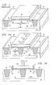
- FIG. 3( a )Shown in FIG. 3( a ) is a further embodiment of the instant invention.
- a n-well region 20is formed in a p-type substrate 10 .
- Isolation structures 30are formed in the n-well region as described above.
- the contact heavily doped contact regions 120are formed in the n-well region following the formation of the gate dielectric layer 100 , the conductive gate layer 110 , and the sidewall structures 125 .
- This structuredoes not have drain and source extension regions.
- the n-type heavily doped contact regions 120can be formed simultaneously with the source and drain regions for a NMOS transistor using the same ion implantation processes.
- FIG. 3( b )Shown in FIG. 3( b ) is the varactor structure shown in FIG. 3( a ) with the additional features of a drain and source extension region 115 . The formation of this drain and source extension region 115 is described above.
- a contiguous PMD layer 130is formed above the gate layers 110 and the contact regions 120 .
- Contact holesare formed in the PMD layer and a conducting material(usually tungsten, aluminum, titanium, copper, and other suitable metals and alloys) is used to fill the contact holes to provide gate layer contacts 140 (or electrical contacts) and contact region contacts 170 .
- the gate layer contacts 140are formed over the active regions 142 of the varactor. Forming the gate layer contacts 140 over the active regions 142 (and thus over the n-well region) reduces the parasitic resistance associated with the varactor and therefore increases the capacitance ratio VR.
- the gate layer contactscan be formed over isolation regions and not over active region of the device structure.
- FIGS. 3 ( a ) and 3 ( b )i.e. without and with the drain and source extension regions 115 ).
- FIG. 3( c )for the case without a drain source extension region 115 .
- a further conducting materialis then formed and patterned on the PMD layer to provide a first network of conducting interconnects for the various contacts on the circuit. Patterned conductor lines are used to interconnect the gate layers 150 and the contact regions 155 to other regions of the integrated circuit.
- a second dielectric layer 160is formed above the first conducting layers 150 , 155 and the PMD layer 130 .
- Via holesare then formed in the second dielectric layer 160 which are filled with a conducting material (usually tungsten, aluminum, titanium, copper, and other suitable metals and alloys) to provide electrical contact to the patterned conducting layers 150 and 155 .
- a conducting materialusually tungsten, aluminum, titanium, copper, and other suitable metals and alloys
- a second patterned conducting layer 190is then formed over the second dielectric layer 160 to provide further interconnects. Additional dielectric layers can be formed above the second dielectric layer is further levels of connectivity are required.
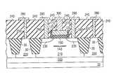
- FIG. 4Shown in FIG. 4 is a further embodiment of the instant invention where the varactor structure is formed in an isolated p-type region 210 in the semiconductor substrate.
- isolation structures 30are formed in the substrate as described above.
- a deep n-well region 200is formed in the substrate to provide isolation for the p-well region 210 that will contain the varactor structure.
- the p-well region 210is formed by first forming a patterned masking film on the substrate followed by ion implanting p-type dopant species into the substrate to form the p-well region 210 .
- the n-well regions 220which will be used to provide contact to the deep n-well region 200 , are formed by implanting n-type dopant species into the substrate through a patterned mask.
- the gate dielectric layer 100 , the gate layer 110 , and the sidewall structures 125are formed as described above.
- the contact regionscan be formed simultaneously with source and drain regions of the PMOS transistors which will be present on the integrated circuit. Alternatively, the p-type contact regions 230 can be formed independently.
- the gate layer contacts 270 and the contact region contacts 260 , and the deep n-well contacts 250are formed as described above.
- the gate layer contacts 270are formed over the active area 143 of the varactor.
- the varactor active area 143can be defined as that region of the varactor where a substantial portion of the depletion region, accumulation layer, or the inversion layer will exist.
- extension regionscan be added to the varactor structure shown in FIG. 4 by implanting p-type dopant species into the substrate after the gate layer 110 is formed.
Landscapes
- Metal-Oxide And Bipolar Metal-Oxide Semiconductor Integrated Circuits (AREA)
- Insulated Gate Type Field-Effect Transistor (AREA)
Abstract
Description
- The present invention relates to a method of forming a metal oxide semiconductor varactor using CMOS technology.[0001]
- In mixed signal applications it is sometimes necessary to have varactors as a part of the CMOS integrated circuit. A varactor is a capacitor whose capacitance value depends on the voltage applied to the capacitor. Typical integrated circuit varactors comprise metal oxide semiconductor (MOS) structures. The capacitor in a MOS structure is formed by the gate electrode (or gate), the gate dielectric layer and the semiconductor substrate. The gate will form one terminal of the capacitor and the semiconductor substrate will form the other terminal. Voltage applied across the gate and the semiconductor substrate will change the value of the capacitor. An important property of a MOS varactor is the ratio of the maximum capacitance of the varactor to the minimum value of capacitance or V[0002]R=Cmax/Cmin. Here Cmaxrepresents the maximum varactor capacitance, Cminthe minimum varactor capacitance, and VRthe varactor capacitance ratio. A number of factors will affect VRincluding gate dielectric thickness, substrate doping, gate electrode doping, series resistance, and frequency of operation. A number of these factors such as gate dielectric thickness, substrate doping, and gate electrode doping also affect the MOS transistors which comprise the integrated circuit and cannot be varied to maximize the capacitance ratio VR. Given the constraint imposed by the other devices comprising the integrated circuit a method is needed to increase the varactor capacitance ratio VRwithout affecting the other integrated circuit devices present.
- The instant invention describes a semiconductor varactor with reduced parasitic resistance. In an embodiment of the invention, a contact isolation structure is formed in a well region. The contacts to the gate layer of the semiconductor are formed over the contact isolation structure thereby reducing the parasitic resistance of the semiconductor structure. This reduction in parasitic resistance results in an increase in the capacitance ratio of the structure compared to the prior art. In another embodiment of the invention, the gate contact is formed over the well region of the semiconductor structure.[0003]
- For a more complete understanding of the present invention and the advantages thereof, reference is now made to the following description taken in conjunction with the accompanying drawings, wherein like reference numerals represent like features, in which:[0004]
- FIG. 1 is cross-section diagram of a portion of an integrated circuit showing a typical MOS varactor.[0005]
- FIGS.[0006]2(a) and2(b) are cross-section diagrams showing a MOS varactor according to an embodiment of the instant invention.
- FIGS.[0007]3(a)-3(c) are cross-section diagrams showing a MOS varactor according to a further embodiment of the instant invention.
- FIG. 4 is a cross-section diagram showing a MOS varactor according to a further embodiment of the instant invention.[0008]
- Illustrated in FIG. 1 is a MOS varactor according to the prior art. A n-well region is formed in a p-[0009]
type semiconductor substrate 10. The n-well region 20 can be formed by implanting n-type dopant species into a region of the p-type substrate. Examples of typical n-type dopant which would be suitable for forming the n-well region 20 are arsenic and phosphorous. The choice of suitable n-type dopants is not however limited to these two species and any n-type dopant species could be used.Isolation structures 30 are formed in the n-well region 20. These isolation structures comprise insulating materials such as silicon oxide and silicon nitride and can be formed using shallow trench isolation (STI) or localized oxidation (LOCOS) techniques. Theisolation structure 30 shown in FIG. 1 is STI. STI structures are typically formed by first forming a trench in the substrate which is then filled with an insulating material usually comprising silicon oxide. In some instances theisolation structures 30 will be formed in the substrate before the n-well region is formed. A gatedielectric layer 40 is then formed on the surface of the substrate. This gatedielectric layer 40 can comprise a material selected from the group consisting of silicon oxide, silicon oxynitride, a silicate, and silicon nitride. In addition alternate layers of these different materials can also be used to form the gate dielectric layer. - Following the formation of the gate[0010]
dielectric layer 40, a gate electrode layer (or gate layer)50 is formed over the gatedielectric layer 40. This gate layer is a conductive layer and usually comprises doped polycrystalline silicon or doped amorphous silicon. In some instances a silicide layer will be formed on thegate layer 50. Following the formation of thegate layer 50, the heavily dopedcontact regions 35 are formed. Thesecontact regions 35 are formed by implanting additional n-type dopants into n-well region 20. These heavily dopedcontact regions 35 will be used to contact the n-well region which will form one terminal of the varactor. In typical CMOS processes, these heavily doped contact regions will be formed using the source and drain region implantation process and the source and drain extension region implantation process. The structure shown in FIG. 1 forms a varactor with anactive area 55. To contact the gate of varactor, contacts are formed to thegate layer 50 outside of theactive area 55. In general, a dielectric layer (usually called a PMD layer) will be formed over thegate layer 50. Contact holes will then be formed in the PMD layer and filled with a conducting material usually referred to as a plug. Tungsten is often used to form these plugs. This conducting material is used to make contact with theunderlying gate layer 50. These additional structures are omitted from FIG. 1 for clarity. The structure of FIG. 1 has a relatively low Q factor due to high parasitic series resistance. - Shown in FIGS.[0011]2(a) and2(b) are cross-section diagrams of a varactor formed according to an embodiment of the instant invention. As described above, a n-
well region 20 andisolation structures 30 are formed in a p-type silicon substrate 10. An additionalcontact isolation structure 32 is formed in the n-well region resulting in the formation ofactive areas dielectric layer 40 and agate layer 50 are then formed over thewell region 20 and the contact isolation structure. The heavily dopedcontact regions 35 are then formed on the surface of the substrate as described above. In forming the heavily dopedcontact region 35, the implant processes used to form the source and drain of NMOS transistors, also present on the integrated circuit, can be used. In addition to heavily doped source and drain regions, NMOS transistors also have more lightly doped drain and source extension regions. In forming these NMOS transistor drain and source extension regions, n-type dopant species are implanted after the gate region of the NMOS transistor is formed. Sidewall structures are then formed adjacent to the NMOS transistor gate region. The source and drain implant processes used to form the NMOS transistor source and drain regions is then performed. This source and drain implant process is therefore self-aligned to the edge of the sidewall regions. The varactor structure shown in FIG. 2(a) is shown without sidewall structures for clarity. In general, the varactor structure will have sidewall structures. In this case sidewallstructures 57 are formed adjacent to thegate layer 50 using standard semiconductor processing and illustrated in FIG. 2(b). This standard sidewall processing includes forming a conformal film comprising silicon nitride or silicon oxide over the gate layer and substrate. The conformal film is then etched using an anisotropic etch process to form thesidewall structures 57. Following the sidewall formation process, the heavily dopedcontact regions 35 are formed as described above. In general the varactor structure in FIGS.2(a) and2(b) will not have lightly doped drain and source extension regions. However such drain and source extension regions can be added to the varactor structure of the instant invention if required. - Following the formation of the varactor structure,[0012]
contact structures 70 are formed to contact thegate layer 50. In forming thecontact structures 70, a PMD layer is formed over entire varactor structure. As described above, contact holes are formed in the PMD layer and conductive plugs are used to fill the contact holes to contact thegate layer 50. As illustrated in FIGS.2(a) and2(b), in an embodiment of the instant invention, thesecontact structures 70 are formed over thecontact isolation structure 32. By forming thecontact structures 70 over thecontact isolation structure 32 of the varactor, the parasitic resistance which was present in the prior art is reduced or eliminated. Reducing the parasitic resistance in the varactor will increase the quality factor Q. This reduction in resistance will become increasingly important as the frequency of the signals used in the varactor increases. - In normal operation, the substrate surface of the active regions of the[0013]
varactor gate layer 50 and the heavily dopedcontact region 35. Depending on the substrate doping type (i.e., n-type or p-type) and voltage applied, the substrate surface in theactive regions - Shown in FIG. 3([0014]a) is a further embodiment of the instant invention. Here a n-
well region 20 is formed in a p-type substrate 10.Isolation structures 30 are formed in the n-well region as described above. The contact heavily dopedcontact regions 120 are formed in the n-well region following the formation of thegate dielectric layer 100, theconductive gate layer 110, and thesidewall structures 125. This structure does not have drain and source extension regions. The n-type heavily dopedcontact regions 120 can be formed simultaneously with the source and drain regions for a NMOS transistor using the same ion implantation processes. Shown in FIG. 3(b) is the varactor structure shown in FIG. 3(a) with the additional features of a drain andsource extension region 115. The formation of this drain andsource extension region 115 is described above. - Following the formation of the varactor structure, a[0015]
contiguous PMD layer 130 is formed above the gate layers110 and thecontact regions 120. Contact holes are formed in the PMD layer and a conducting material(usually tungsten, aluminum, titanium, copper, and other suitable metals and alloys) is used to fill the contact holes to provide gate layer contacts140 (or electrical contacts) andcontact region contacts 170. In an embodiment, thegate layer contacts 140 are formed over theactive regions 142 of the varactor. Forming thegate layer contacts 140 over the active regions142 (and thus over the n-well region) reduces the parasitic resistance associated with the varactor and therefore increases the capacitance ratio VR. In a further embodiment, the gate layer contacts can be formed over isolation regions and not over active region of the device structure. This will apply to the structures shown in FIGS.3(a) and3(b) (i.e. without and with the drain and source extension regions115). This is shown in FIG. 3(c) for the case without a drainsource extension region 115. Following the formation of the gate layer contacts, a further conducting material is then formed and patterned on the PMD layer to provide a first network of conducting interconnects for the various contacts on the circuit. Patterned conductor lines are used to interconnect the gate layers150 and thecontact regions 155 to other regions of the integrated circuit. Asecond dielectric layer 160 is formed above the first conducting layers150,155 and thePMD layer 130. Via holes are then formed in thesecond dielectric layer 160 which are filled with a conducting material (usually tungsten, aluminum, titanium, copper, and other suitable metals and alloys) to provide electrical contact to the patterned conductinglayers patterned conducting layer 190 is then formed over thesecond dielectric layer 160 to provide further interconnects. Additional dielectric layers can be formed above the second dielectric layer is further levels of connectivity are required. - Shown in FIG. 4 is a further embodiment of the instant invention where the varactor structure is formed in an isolated p-[0016]
type region 210 in the semiconductor substrate. In forming the embodiment shown in FIG. 4,isolation structures 30 are formed in the substrate as described above. A deep n-well region 200 is formed in the substrate to provide isolation for the p-well region 210 that will contain the varactor structure. The p-well region 210 is formed by first forming a patterned masking film on the substrate followed by ion implanting p-type dopant species into the substrate to form the p-well region 210. The n-well regions 220 which will be used to provide contact to the deep n-well region 200, are formed by implanting n-type dopant species into the substrate through a patterned mask. Thegate dielectric layer 100, thegate layer 110, and thesidewall structures 125 are formed as described above. The contact regions can be formed simultaneously with source and drain regions of the PMOS transistors which will be present on the integrated circuit. Alternatively, the p-type contact regions 230 can be formed independently. Following the formation of thePMD layer 240, thegate layer contacts 270 and thecontact region contacts 260, and the deep n-well contacts 250 are formed as described above. Thegate layer contacts 270 are formed over theactive area 143 of the varactor. As described above, the varactoractive area 143 can be defined as that region of the varactor where a substantial portion of the depletion region, accumulation layer, or the inversion layer will exist. In addition to the above described process, extension regions can be added to the varactor structure shown in FIG. 4 by implanting p-type dopant species into the substrate after thegate layer 110 is formed. - While this invention has been described with reference to illustrative embodiments, this description is not intended to be construed in a limiting sense. Various modifications and combinations of the illustrative embodiments, as well as other embodiments of the invention will be apparent to persons skilled in the art upon reference to the description. It is therefore intended that the appended claims encompass any such modifications or embodiments.[0017]
Claims (22)
1. A method of forming a semiconductor varactor, comprising:
forming a well region of a first conductivity type in a semiconductor substrate;
forming a gate dielectric layer on said well region;
forming a gate layer on said gate dielectric layer;
forming contact regions in said well region of a first conductivity type; and
forming gate layer contacts to said gate conductive layer wherein said gate layer contacts overlie said well region.
2. The method ofclaim 1 further comprising forming sidewall structures adjacent to said gate layer.
3. The method ofclaim 2 wherein said well region is n-type.
4. The method ofclaim 2 wherein said well region is p-type.
5. The method ofclaim 1 wherein said forming gate layer contacts comprises forming said gate layer contacts to said gate layer over an active area of said semiconductor varactor.
6. A semiconductor varactor, comprising:
a well region of a first conductivity type in a semiconductor substrate;
a gate dielectric layer on said well region;
a gate layer on said gate dielectric layer;
contact regions in said well region of a first conductivity type; and
gate layer contacts to said gate layer wherein said gate contacts overlie said well region.
7. The semiconductor varactor ofclaim 6 further comprising sidewall structures adjacent to said gate layer.
8. The semiconductor varactor ofclaim 7 wherein said well region is n-type.
9. The semiconductor varactor ofclaim 7 wherein said well region is p-type.
10. The semiconductor varactor ofclaim 6 wherein said gate layer contacts comprises gate layer contacts to said gate layer over an active region of said semiconductor varactor.
11. A method for forming a low resistance semiconductor varactor, comprising
providing a semiconductor substrate with at least a first isolation region and a second isolation region separated by a first distance;
forming a well region in said semiconductor substrate between said first isolation region and said second isolation region;
forming a contact isolation structure in said well region between said first isolation region and said second isolation region;
forming a gate dielectric layer on said well region and said contact isolation region;
forming a gate layer on said gate dielectric layer wherein said gate layer overlies said contact isolation region; and
forming electrical contacts to said gate conductive layer over said contact isolation region.
12. The method ofclaim 11 wherein said first and second isolation regions comprise STI structures.
13. The method ofclaim 11 wherein said contact isolation structure comprises a STI structure.
14. The method ofclaim 11 further comprising forming well contact regions adjacent to said first and second isolation regions.
15. A low resistance semiconductor varactor, comprising
providing a semiconductor substrate with at least a first isolation region and a second isolation region separated by a first distance;
a well region in said semiconductor substrate between said first isolation region and said second isolation region;
a contact isolation structure in said well region between said first isolation region and said second isolation region;
a gate dielectric layer on said well region and said contact isolation region;
a gate layer on said gate dielectric layer wherein said gate layer overlies said contact isolation region; and
electrical contacts to said gate conductive layer over said contact isolation region.
16. The varactor ofclaim 15 wherein said first and second isolation regions comprise STI structures.
17. The method ofclaim 15 wherein said contact isolation structure comprises a STI structure.
18. The method ofclaim 15 further comprising well contact regions adjacent to said first and second isolation regions.
19. A method of forming a semiconductor varactor, comprising:
forming a well region of a first conductivity type in a semiconductor substrate;
forming a gate dielectric layer on said well region; forming a gate layer on said gate dielectric layer;
forming contact regions in said well region of a first conductivity type wherein said contact regions are formed using a source and drain region implantation formation process; and
forming gate layer contacts to said gate conductive layer wherein said gate layer contacts overlie an isolation region
20. The method ofclaim 19 further comprising forming sidewall structures adjacent to said gate layer.
21. The method ofclaim 20 wherein said well region is n-type.
22. The method ofclaim 20 wherein said well region is p-type.
Priority Applications (3)
| Application Number | Priority Date | Filing Date | Title |
|---|---|---|---|
| US09/994,421US7053465B2 (en) | 2000-11-28 | 2001-11-27 | Semiconductor varactor with reduced parasitic resistance |
| US11/395,385US20060192268A1 (en) | 2000-11-28 | 2006-03-31 | Semiconductor varactor with reduced parasitic resistance |
| US12/796,206US20100244138A1 (en) | 2000-11-28 | 2010-06-08 | Semiconductor varactor with reduced parasitic resistance |
Applications Claiming Priority (2)
| Application Number | Priority Date | Filing Date | Title |
|---|---|---|---|
| US25362000P | 2000-11-28 | 2000-11-28 | |
| US09/994,421US7053465B2 (en) | 2000-11-28 | 2001-11-27 | Semiconductor varactor with reduced parasitic resistance |
Related Child Applications (1)
| Application Number | Title | Priority Date | Filing Date |
|---|---|---|---|
| US11/395,385DivisionUS20060192268A1 (en) | 2000-11-28 | 2006-03-31 | Semiconductor varactor with reduced parasitic resistance |
Publications (2)
| Publication Number | Publication Date |
|---|---|
| US20020074589A1true US20020074589A1 (en) | 2002-06-20 |
| US7053465B2 US7053465B2 (en) | 2006-05-30 |
Family
ID=26943419
Family Applications (3)
| Application Number | Title | Priority Date | Filing Date |
|---|---|---|---|
| US09/994,421Expired - LifetimeUS7053465B2 (en) | 2000-11-28 | 2001-11-27 | Semiconductor varactor with reduced parasitic resistance |
| US11/395,385AbandonedUS20060192268A1 (en) | 2000-11-28 | 2006-03-31 | Semiconductor varactor with reduced parasitic resistance |
| US12/796,206AbandonedUS20100244138A1 (en) | 2000-11-28 | 2010-06-08 | Semiconductor varactor with reduced parasitic resistance |
Family Applications After (2)
| Application Number | Title | Priority Date | Filing Date |
|---|---|---|---|
| US11/395,385AbandonedUS20060192268A1 (en) | 2000-11-28 | 2006-03-31 | Semiconductor varactor with reduced parasitic resistance |
| US12/796,206AbandonedUS20100244138A1 (en) | 2000-11-28 | 2010-06-08 | Semiconductor varactor with reduced parasitic resistance |
Country Status (1)
| Country | Link |
|---|---|
| US (3) | US7053465B2 (en) |
Cited By (20)
| Publication number | Priority date | Publication date | Assignee | Title |
|---|---|---|---|---|
| US20030137796A1 (en)* | 2002-01-18 | 2003-07-24 | Constantin Bulucea | Gate-enhanced junction varactor with gradual capacitance variation |
| US20040184216A1 (en)* | 2003-01-31 | 2004-09-23 | Nec Electronics Corporation | Voltage controlled variable capacitance device |
| US20040195643A1 (en)* | 2003-04-01 | 2004-10-07 | Texas Instruments Incorporated | Variable reactor (varactor) with engineered capacitance-voltage characteristics |
| US20040203213A1 (en)* | 2003-03-25 | 2004-10-14 | Yi-Sun Chung | Method for manufacturing an MOS varactor |
| US20050133826A1 (en)* | 2003-03-21 | 2005-06-23 | Krishnan Anand T. | Semiconductor antenna proximity lines |
| US20060006434A1 (en)* | 2001-08-24 | 2006-01-12 | Renesas Technology Corp. | Semiconductor device including insulated gate type transistor and insulated gate type capacitance, and method of manufacturing the same |
| US20060043454A1 (en)* | 2004-08-27 | 2006-03-02 | International Business Machines Corporation | Mos varactor using isolation well |
| US7067384B1 (en)* | 2001-05-24 | 2006-06-27 | National Semiconductor Corporation | Method of forming a varactor with an increased linear tuning range |
| US20060220181A1 (en)* | 2005-04-01 | 2006-10-05 | Taiwan Semiconductor Manufacturing Co., Ltd. | Controllable varactor within dummy substrate pattern |
| US20070004158A1 (en)* | 2003-11-05 | 2007-01-04 | Texas Instruments Incorporated | Transistor having a germanium implant region located therein and a method of manufacture therefor |
| US20070013026A1 (en)* | 2005-07-12 | 2007-01-18 | Ching-Hung Kao | Varactor structure and method for fabricating the same |
| US20070029587A1 (en)* | 2005-08-08 | 2007-02-08 | International Business Machines Corporation | Mos varactor with segmented gate doping |
| US20070096170A1 (en)* | 2005-11-02 | 2007-05-03 | International Business Machines Corporation | Low modulus spacers for channel stress enhancement |
| US20070232010A1 (en)* | 2004-08-27 | 2007-10-04 | Ching-Hung Kao | Method for fabricating a junction varactor with high q factor |
| US20080079051A1 (en)* | 2006-09-29 | 2008-04-03 | Luo Yuan | Varactor with halo implant regions of opposite polarity |
| US20120319206A1 (en)* | 2011-06-16 | 2012-12-20 | Stmicroelectronics (Crolles 2) Sas | Integrated circuit comprising an isolating trench and corresponding method |
| US20180006163A1 (en)* | 2016-07-01 | 2018-01-04 | Taiwan Semiconductor Manufacturing Company Ltd. | Mos capacitor, semiconductor fabrication method and mos capacitor circuit |
| CN110754003A (en)* | 2017-06-19 | 2020-02-04 | 高通股份有限公司 | Self-Aligned Contacts (SACs) on Gates for Improved Quality Factor of Metal-Oxide-Semiconductor (MOS) varactors |
| US10586878B2 (en)* | 2015-04-15 | 2020-03-10 | Futurewei Technologies, Inc. | Apparatus and method for a low loss coupling capacitor |
| US20220336683A1 (en)* | 2019-09-17 | 2022-10-20 | Taiwan Semiconductor Manufacturing Company, Ltd. | Method of making decoupling capacitor |
Families Citing this family (13)
| Publication number | Priority date | Publication date | Assignee | Title |
|---|---|---|---|---|
| JP2009094248A (en)* | 2007-10-05 | 2009-04-30 | Toshiba Corp | Semiconductor device and manufacturing method thereof |
| US8115281B2 (en)* | 2008-05-20 | 2012-02-14 | Atmel Corporation | Differential varactor |
| US20100019351A1 (en)* | 2008-07-28 | 2010-01-28 | Albert Ratnakumar | Varactors with enhanced tuning ranges |
| US8513119B2 (en) | 2008-12-10 | 2013-08-20 | Taiwan Semiconductor Manufacturing Company, Ltd. | Method of forming bump structure having tapered sidewalls for stacked dies |
| US20100171197A1 (en) | 2009-01-05 | 2010-07-08 | Hung-Pin Chang | Isolation Structure for Stacked Dies |
| US8362568B2 (en)* | 2009-08-28 | 2013-01-29 | International Business Machines Corporation | Recessed contact for multi-gate FET optimizing series resistance |
| US8791549B2 (en) | 2009-09-22 | 2014-07-29 | Taiwan Semiconductor Manufacturing Company, Ltd. | Wafer backside interconnect structure connected to TSVs |
| CN102122654B (en)* | 2010-01-08 | 2012-12-05 | 中芯国际集成电路制造(上海)有限公司 | Varactor and manufacturing method thereof |
| US8273616B2 (en) | 2010-02-19 | 2012-09-25 | Taiwan Semiconductor Manufacturing Company, Ltd. | Gated-varactors |
| US8466059B2 (en) | 2010-03-30 | 2013-06-18 | Taiwan Semiconductor Manufacturing Company, Ltd. | Multi-layer interconnect structure for stacked dies |
| US8450827B2 (en) | 2011-01-25 | 2013-05-28 | Taiwan Semiconductor Manufacturing Company, Ltd. | MOS varactor structure and methods |
| US8900994B2 (en) | 2011-06-09 | 2014-12-02 | Taiwan Semiconductor Manufacturing Company, Ltd. | Method for producing a protective structure |
| US11121129B2 (en)* | 2018-07-31 | 2021-09-14 | Taiwan Semiconductor Manufacturing Company, Ltd. | Semiconductor device |
Citations (3)
| Publication number | Priority date | Publication date | Assignee | Title |
|---|---|---|---|---|
| US5910673A (en)* | 1997-12-04 | 1999-06-08 | Sharp Microelectronics Technology, Inc. | Locos MOS device for ESD protection |
| US6316805B1 (en)* | 2000-01-06 | 2001-11-13 | Vanguard International Semiconductor Corporation | Electrostatic discharge device with gate-controlled field oxide transistor |
| US6351020B1 (en)* | 1999-11-12 | 2002-02-26 | Motorola, Inc. | Linear capacitor structure in a CMOS process |
Family Cites Families (5)
| Publication number | Priority date | Publication date | Assignee | Title |
|---|---|---|---|---|
| JP3244065B2 (en)* | 1998-10-23 | 2002-01-07 | 日本電気株式会社 | Semiconductor electrostatic protection element and method of manufacturing the same |
| US6268778B1 (en)* | 1999-05-03 | 2001-07-31 | Silicon Wave, Inc. | Method and apparatus for fully integrating a voltage controlled oscillator on an integrated circuit |
| DE19920983C5 (en)* | 1999-05-06 | 2004-11-18 | Fibermark Gessner Gmbh & Co. Ohg | Two-layer or multi-layer filter medium for air filtration and filter element made from it |
| US6214656B1 (en)* | 1999-05-17 | 2001-04-10 | Taiwian Semiconductor Manufacturing Company | Partial silicide gate in sac (self-aligned contact) process |
| US6399427B1 (en)* | 2000-02-24 | 2002-06-04 | Advanced Micro Devices, Inc. | Formation of ultra-thin active device area on semiconductor on insulator (SOI) substrate |
- 2001
- 2001-11-27USUS09/994,421patent/US7053465B2/ennot_activeExpired - Lifetime
- 2006
- 2006-03-31USUS11/395,385patent/US20060192268A1/ennot_activeAbandoned
- 2010
- 2010-06-08USUS12/796,206patent/US20100244138A1/ennot_activeAbandoned
Patent Citations (3)
| Publication number | Priority date | Publication date | Assignee | Title |
|---|---|---|---|---|
| US5910673A (en)* | 1997-12-04 | 1999-06-08 | Sharp Microelectronics Technology, Inc. | Locos MOS device for ESD protection |
| US6351020B1 (en)* | 1999-11-12 | 2002-02-26 | Motorola, Inc. | Linear capacitor structure in a CMOS process |
| US6316805B1 (en)* | 2000-01-06 | 2001-11-13 | Vanguard International Semiconductor Corporation | Electrostatic discharge device with gate-controlled field oxide transistor |
Cited By (46)
| Publication number | Priority date | Publication date | Assignee | Title |
|---|---|---|---|---|
| US7067384B1 (en)* | 2001-05-24 | 2006-06-27 | National Semiconductor Corporation | Method of forming a varactor with an increased linear tuning range |
| US7456464B2 (en) | 2001-08-24 | 2008-11-25 | Renesas Technology Corp. | Semiconductor device including insulated gate type transistor and insulated gate type variable capacitance, and method of manufacturing the same |
| US20070108494A1 (en)* | 2001-08-24 | 2007-05-17 | Renesas Technology Corp. | Semiconductor device including insulated gate type transistor and insulated gate type capacitance, and method of manufacturing the same |
| US7176515B2 (en) | 2001-08-24 | 2007-02-13 | Renesas Technology Corp. | Semiconductor device including insulated gate type transistor and insulated gate type capacitance having protruded portions |
| US7157765B2 (en)* | 2001-08-24 | 2007-01-02 | Renesas Technology Corp. | Semiconductor device including insulated gate type transistor with pocket regions and insulated gate type capacitor with no region of reverse conductivity type |
| US20060267105A1 (en)* | 2001-08-24 | 2006-11-30 | Renesas Technology Corp. | Semiconductor device including insulated gate type transistor and insulated gate type capacitance, and method of manufacturing the same |
| US20060006434A1 (en)* | 2001-08-24 | 2006-01-12 | Renesas Technology Corp. | Semiconductor device including insulated gate type transistor and insulated gate type capacitance, and method of manufacturing the same |
| US7078787B1 (en) | 2002-01-18 | 2006-07-18 | National Semiconductor Corporation | Design and operation of gate-enhanced junction varactor with gradual capacitance variation |
| US20030137796A1 (en)* | 2002-01-18 | 2003-07-24 | Constantin Bulucea | Gate-enhanced junction varactor with gradual capacitance variation |
| US7081663B2 (en)* | 2002-01-18 | 2006-07-25 | National Semiconductor Corporation | Gate-enhanced junction varactor with gradual capacitance variation |
| US6999296B2 (en)* | 2003-01-31 | 2006-02-14 | Nec Electronics Corporation | Voltage controlled variable capacitance device |
| US20040184216A1 (en)* | 2003-01-31 | 2004-09-23 | Nec Electronics Corporation | Voltage controlled variable capacitance device |
| US7071092B2 (en)* | 2003-03-21 | 2006-07-04 | Texas Instruments Incorporated | Method of manufacturing antenna proximity lines |
| US20050133826A1 (en)* | 2003-03-21 | 2005-06-23 | Krishnan Anand T. | Semiconductor antenna proximity lines |
| US20040203213A1 (en)* | 2003-03-25 | 2004-10-14 | Yi-Sun Chung | Method for manufacturing an MOS varactor |
| US20040195643A1 (en)* | 2003-04-01 | 2004-10-07 | Texas Instruments Incorporated | Variable reactor (varactor) with engineered capacitance-voltage characteristics |
| US6847095B2 (en)* | 2003-04-01 | 2005-01-25 | Texas Instruments Incorporated | Variable reactor (varactor) with engineered capacitance-voltage characteristics |
| US20070004158A1 (en)* | 2003-11-05 | 2007-01-04 | Texas Instruments Incorporated | Transistor having a germanium implant region located therein and a method of manufacture therefor |
| JP2008511989A (en)* | 2004-08-27 | 2008-04-17 | インターナショナル・ビジネス・マシーンズ・コーポレーション | MOS varactor using isolation well |
| EP1800343A4 (en)* | 2004-08-27 | 2008-11-19 | Ibm | VARACTOR MOS USING AN ISOLATION WELL |
| US7714412B2 (en) | 2004-08-27 | 2010-05-11 | International Business Machines Corporation | MOS varactor using isolation well |
| KR101013251B1 (en)* | 2004-08-27 | 2011-02-09 | 인터내셔널 비지네스 머신즈 코포레이션 | MOOS varactors using separation wells |
| WO2006026055A3 (en)* | 2004-08-27 | 2006-12-14 | Ibm | Mos varactor using isolation well |
| US20070232010A1 (en)* | 2004-08-27 | 2007-10-04 | Ching-Hung Kao | Method for fabricating a junction varactor with high q factor |
| US7378327B2 (en)* | 2004-08-27 | 2008-05-27 | United Microelectronics Corp. | Method for fabricating a junction varactor with high Q factor |
| US20060043454A1 (en)* | 2004-08-27 | 2006-03-02 | International Business Machines Corporation | Mos varactor using isolation well |
| US20060220181A1 (en)* | 2005-04-01 | 2006-10-05 | Taiwan Semiconductor Manufacturing Co., Ltd. | Controllable varactor within dummy substrate pattern |
| US7525177B2 (en)* | 2005-04-01 | 2009-04-28 | Taiwan Semiconductor Manufacturing Co., Ltd. | Controllable varactor within dummy substrate pattern |
| US20080003758A1 (en)* | 2005-07-12 | 2008-01-03 | Ching-Hung Kao | Varactor structure and method for fabricating the same |
| US20070013026A1 (en)* | 2005-07-12 | 2007-01-18 | Ching-Hung Kao | Varactor structure and method for fabricating the same |
| US20070029587A1 (en)* | 2005-08-08 | 2007-02-08 | International Business Machines Corporation | Mos varactor with segmented gate doping |
| US7545007B2 (en)* | 2005-08-08 | 2009-06-09 | International Business Machines Corporation | MOS varactor with segmented gate doping |
| US20070096170A1 (en)* | 2005-11-02 | 2007-05-03 | International Business Machines Corporation | Low modulus spacers for channel stress enhancement |
| US20080079051A1 (en)* | 2006-09-29 | 2008-04-03 | Luo Yuan | Varactor with halo implant regions of opposite polarity |
| US20120319206A1 (en)* | 2011-06-16 | 2012-12-20 | Stmicroelectronics (Crolles 2) Sas | Integrated circuit comprising an isolating trench and corresponding method |
| US8829622B2 (en)* | 2011-06-16 | 2014-09-09 | Stmicroelectronics (Crolles 2) Sas | Integrated circuit comprising an isolating trench and corresponding method |
| US9117876B2 (en) | 2011-06-16 | 2015-08-25 | Stmicroelectronics (Crolles 2) Sas | Integrated circuit comprising an isolating trench and corresponding method |
| US10586878B2 (en)* | 2015-04-15 | 2020-03-10 | Futurewei Technologies, Inc. | Apparatus and method for a low loss coupling capacitor |
| US11569393B2 (en) | 2015-04-15 | 2023-01-31 | Futurewei Technologies, Inc. | Apparatus and method for a low loss coupling capacitor |
| US20180006163A1 (en)* | 2016-07-01 | 2018-01-04 | Taiwan Semiconductor Manufacturing Company Ltd. | Mos capacitor, semiconductor fabrication method and mos capacitor circuit |
| US10510906B2 (en)* | 2016-07-01 | 2019-12-17 | Taiwan Semiconductor Manufacturing Company Ltd. | MOS capacitor, semiconductor fabrication method and MOS capacitor circuit |
| CN110754003A (en)* | 2017-06-19 | 2020-02-04 | 高通股份有限公司 | Self-Aligned Contacts (SACs) on Gates for Improved Quality Factor of Metal-Oxide-Semiconductor (MOS) varactors |
| US20220336683A1 (en)* | 2019-09-17 | 2022-10-20 | Taiwan Semiconductor Manufacturing Company, Ltd. | Method of making decoupling capacitor |
| US20230387329A1 (en)* | 2019-09-17 | 2023-11-30 | Taiwan Semiconductor Manufacturing Company, Ltd. | Method of making decoupling capacitor |
| US11901463B2 (en)* | 2019-09-17 | 2024-02-13 | Taiwan Semiconductor Manufacturing Company, Ltd. | Method of making decoupling capacitor |
| US12310038B2 (en)* | 2019-09-17 | 2025-05-20 | Taiwan Semiconductor Manufacturing Company, Ltd. | Method of making decoupling capacitor |
Also Published As
| Publication number | Publication date |
|---|---|
| US20100244138A1 (en) | 2010-09-30 |
| US7053465B2 (en) | 2006-05-30 |
| US20060192268A1 (en) | 2006-08-31 |
Similar Documents
| Publication | Publication Date | Title |
|---|---|---|
| US7053465B2 (en) | Semiconductor varactor with reduced parasitic resistance | |
| JP3516442B2 (en) | Structure and process integration for producing transistors with independently adjustable parameters | |
| US5773358A (en) | Method of forming a field effect transistor and method of forming CMOS integrated circuitry | |
| US5538913A (en) | Process for fabricating MOS transistors having full-overlap lightly-doped drain structure | |
| KR100296004B1 (en) | Semiconductor device and method for manufacturing the same | |
| US7193262B2 (en) | Low-cost deep trench decoupling capacitor device and process of manufacture | |
| US5714393A (en) | Diode-connected semiconductor device and method of manufacture | |
| US6372562B1 (en) | Method of producing a semiconductor device | |
| US5930616A (en) | Methods of forming a field effect transistor and method of forming CMOS circuitry | |
| US20020081820A1 (en) | Method for manufacturing semiconductor device capable of suppressing narrow channel width effect | |
| KR20010092309A (en) | Decoupling capacitors and methods for forming the same | |
| US5612240A (en) | Method for making electrical connections to self-aligned contacts that extends beyond the photo-lithographic resolution limit | |
| JP2001110911A (en) | Semiconductor device having SOI structure and method of manufacturing the same | |
| KR100823821B1 (en) | Manufacturing Method of Semiconductor Integrated Circuit Device | |
| US20060289904A1 (en) | Semiconductor device and method of manufacturing the same | |
| US6555915B1 (en) | Integrated circuit having interconnect to a substrate and method therefor | |
| US20010002058A1 (en) | Semiconductor apparatus and method of manufacture | |
| WO2004066367A2 (en) | Low-gidl mosfet structure and method for fabrication | |
| US5432105A (en) | Method for fabricating self-aligned polysilicon contacts on FET source/drain areas | |
| US5661048A (en) | Method of making an insulated gate semiconductor device | |
| US12432944B2 (en) | Semiconductor device structure and method for forming same | |
| US5970331A (en) | Method of making a plug transistor | |
| US6486516B1 (en) | Semiconductor device and a method of producing the same | |
| US6162690A (en) | Methods of forming field effect transistors having self-aligned intermediate source and drain contacts | |
| JP2845186B2 (en) | Semiconductor device and manufacturing method thereof |
Legal Events
| Date | Code | Title | Description |
|---|---|---|---|
| AS | Assignment | Owner name:TEXAS INSTRUMENTS INCORPORATED, TEXAS Free format text:ASSIGNMENT OF ASSIGNORS INTEREST;ASSIGNORS:BENAISSA, KAMEL;SHEN, CHI-CHEONG;REEL/FRAME:012329/0566 Effective date:20001205 | |
| STCF | Information on status: patent grant | Free format text:PATENTED CASE | |
| FPAY | Fee payment | Year of fee payment:4 | |
| FPAY | Fee payment | Year of fee payment:8 | |
| MAFP | Maintenance fee payment | Free format text:PAYMENT OF MAINTENANCE FEE, 12TH YEAR, LARGE ENTITY (ORIGINAL EVENT CODE: M1553) Year of fee payment:12 |