US20020074552A1 - Gallium nitride materials and methods - Google Patents
Gallium nitride materials and methodsDownload PDFInfo
- Publication number
- US20020074552A1 US20020074552A1US09/736,972US73697200AUS2002074552A1US 20020074552 A1US20020074552 A1US 20020074552A1US 73697200 AUS73697200 AUS 73697200AUS 2002074552 A1US2002074552 A1US 2002074552A1
- Authority
- US
- United States
- Prior art keywords
- gallium nitride
- layer
- semiconductor material
- nitride material
- semiconductor
- Prior art date
- Legal status (The legal status is an assumption and is not a legal conclusion. Google has not performed a legal analysis and makes no representation as to the accuracy of the status listed.)
- Granted
Links
Images


Classifications
- C—CHEMISTRY; METALLURGY
- C30—CRYSTAL GROWTH
- C30B—SINGLE-CRYSTAL GROWTH; UNIDIRECTIONAL SOLIDIFICATION OF EUTECTIC MATERIAL OR UNIDIRECTIONAL DEMIXING OF EUTECTOID MATERIAL; REFINING BY ZONE-MELTING OF MATERIAL; PRODUCTION OF A HOMOGENEOUS POLYCRYSTALLINE MATERIAL WITH DEFINED STRUCTURE; SINGLE CRYSTALS OR HOMOGENEOUS POLYCRYSTALLINE MATERIAL WITH DEFINED STRUCTURE; AFTER-TREATMENT OF SINGLE CRYSTALS OR A HOMOGENEOUS POLYCRYSTALLINE MATERIAL WITH DEFINED STRUCTURE; APPARATUS THEREFOR
- C30B23/00—Single-crystal growth by condensing evaporated or sublimed materials
- C30B23/02—Epitaxial-layer growth
- H—ELECTRICITY
- H10—SEMICONDUCTOR DEVICES; ELECTRIC SOLID-STATE DEVICES NOT OTHERWISE PROVIDED FOR
- H10D—INORGANIC ELECTRIC SEMICONDUCTOR DEVICES
- H10D62/00—Semiconductor bodies, or regions thereof, of devices having potential barriers
- H10D62/80—Semiconductor bodies, or regions thereof, of devices having potential barriers characterised by the materials
- H10D62/81—Semiconductor bodies, or regions thereof, of devices having potential barriers characterised by the materials of structures exhibiting quantum-confinement effects, e.g. single quantum wells; of structures having periodic or quasi-periodic potential variation
- H10D62/815—Semiconductor bodies, or regions thereof, of devices having potential barriers characterised by the materials of structures exhibiting quantum-confinement effects, e.g. single quantum wells; of structures having periodic or quasi-periodic potential variation of structures having periodic or quasi-periodic potential variation, e.g. superlattices or multiple quantum wells [MQW]
- H10D62/8161—Semiconductor bodies, or regions thereof, of devices having potential barriers characterised by the materials of structures exhibiting quantum-confinement effects, e.g. single quantum wells; of structures having periodic or quasi-periodic potential variation of structures having periodic or quasi-periodic potential variation, e.g. superlattices or multiple quantum wells [MQW] potential variation due to variations in composition or crystallinity, e.g. heterojunction superlattices
- H10D62/8162—Semiconductor bodies, or regions thereof, of devices having potential barriers characterised by the materials of structures exhibiting quantum-confinement effects, e.g. single quantum wells; of structures having periodic or quasi-periodic potential variation of structures having periodic or quasi-periodic potential variation, e.g. superlattices or multiple quantum wells [MQW] potential variation due to variations in composition or crystallinity, e.g. heterojunction superlattices having quantum effects only in the vertical direction, i.e. layered structures having quantum effects solely resulting from vertical potential variation
- H10D62/8164—Semiconductor bodies, or regions thereof, of devices having potential barriers characterised by the materials of structures exhibiting quantum-confinement effects, e.g. single quantum wells; of structures having periodic or quasi-periodic potential variation of structures having periodic or quasi-periodic potential variation, e.g. superlattices or multiple quantum wells [MQW] potential variation due to variations in composition or crystallinity, e.g. heterojunction superlattices having quantum effects only in the vertical direction, i.e. layered structures having quantum effects solely resulting from vertical potential variation comprising only semiconductor materials
- C—CHEMISTRY; METALLURGY
- C30—CRYSTAL GROWTH
- C30B—SINGLE-CRYSTAL GROWTH; UNIDIRECTIONAL SOLIDIFICATION OF EUTECTIC MATERIAL OR UNIDIRECTIONAL DEMIXING OF EUTECTOID MATERIAL; REFINING BY ZONE-MELTING OF MATERIAL; PRODUCTION OF A HOMOGENEOUS POLYCRYSTALLINE MATERIAL WITH DEFINED STRUCTURE; SINGLE CRYSTALS OR HOMOGENEOUS POLYCRYSTALLINE MATERIAL WITH DEFINED STRUCTURE; AFTER-TREATMENT OF SINGLE CRYSTALS OR A HOMOGENEOUS POLYCRYSTALLINE MATERIAL WITH DEFINED STRUCTURE; APPARATUS THEREFOR
- C30B23/00—Single-crystal growth by condensing evaporated or sublimed materials
- C30B23/02—Epitaxial-layer growth
- C30B23/025—Epitaxial-layer growth characterised by the substrate
- C—CHEMISTRY; METALLURGY
- C30—CRYSTAL GROWTH
- C30B—SINGLE-CRYSTAL GROWTH; UNIDIRECTIONAL SOLIDIFICATION OF EUTECTIC MATERIAL OR UNIDIRECTIONAL DEMIXING OF EUTECTOID MATERIAL; REFINING BY ZONE-MELTING OF MATERIAL; PRODUCTION OF A HOMOGENEOUS POLYCRYSTALLINE MATERIAL WITH DEFINED STRUCTURE; SINGLE CRYSTALS OR HOMOGENEOUS POLYCRYSTALLINE MATERIAL WITH DEFINED STRUCTURE; AFTER-TREATMENT OF SINGLE CRYSTALS OR A HOMOGENEOUS POLYCRYSTALLINE MATERIAL WITH DEFINED STRUCTURE; APPARATUS THEREFOR
- C30B25/00—Single-crystal growth by chemical reaction of reactive gases, e.g. chemical vapour-deposition growth
- C30B25/02—Epitaxial-layer growth
- C30B25/18—Epitaxial-layer growth characterised by the substrate
- C30B25/183—Epitaxial-layer growth characterised by the substrate being provided with a buffer layer, e.g. a lattice matching layer
- C—CHEMISTRY; METALLURGY
- C30—CRYSTAL GROWTH
- C30B—SINGLE-CRYSTAL GROWTH; UNIDIRECTIONAL SOLIDIFICATION OF EUTECTIC MATERIAL OR UNIDIRECTIONAL DEMIXING OF EUTECTOID MATERIAL; REFINING BY ZONE-MELTING OF MATERIAL; PRODUCTION OF A HOMOGENEOUS POLYCRYSTALLINE MATERIAL WITH DEFINED STRUCTURE; SINGLE CRYSTALS OR HOMOGENEOUS POLYCRYSTALLINE MATERIAL WITH DEFINED STRUCTURE; AFTER-TREATMENT OF SINGLE CRYSTALS OR A HOMOGENEOUS POLYCRYSTALLINE MATERIAL WITH DEFINED STRUCTURE; APPARATUS THEREFOR
- C30B29/00—Single crystals or homogeneous polycrystalline material with defined structure characterised by the material or by their shape
- C30B29/02—Elements
- C30B29/06—Silicon
- C—CHEMISTRY; METALLURGY
- C30—CRYSTAL GROWTH
- C30B—SINGLE-CRYSTAL GROWTH; UNIDIRECTIONAL SOLIDIFICATION OF EUTECTIC MATERIAL OR UNIDIRECTIONAL DEMIXING OF EUTECTOID MATERIAL; REFINING BY ZONE-MELTING OF MATERIAL; PRODUCTION OF A HOMOGENEOUS POLYCRYSTALLINE MATERIAL WITH DEFINED STRUCTURE; SINGLE CRYSTALS OR HOMOGENEOUS POLYCRYSTALLINE MATERIAL WITH DEFINED STRUCTURE; AFTER-TREATMENT OF SINGLE CRYSTALS OR A HOMOGENEOUS POLYCRYSTALLINE MATERIAL WITH DEFINED STRUCTURE; APPARATUS THEREFOR
- C30B29/00—Single crystals or homogeneous polycrystalline material with defined structure characterised by the material or by their shape
- C30B29/10—Inorganic compounds or compositions
- C30B29/40—AIIIBV compounds wherein A is B, Al, Ga, In or Tl and B is N, P, As, Sb or Bi
- C30B29/403—AIII-nitrides
- C30B29/406—Gallium nitride
- C—CHEMISTRY; METALLURGY
- C30—CRYSTAL GROWTH
- C30B—SINGLE-CRYSTAL GROWTH; UNIDIRECTIONAL SOLIDIFICATION OF EUTECTIC MATERIAL OR UNIDIRECTIONAL DEMIXING OF EUTECTOID MATERIAL; REFINING BY ZONE-MELTING OF MATERIAL; PRODUCTION OF A HOMOGENEOUS POLYCRYSTALLINE MATERIAL WITH DEFINED STRUCTURE; SINGLE CRYSTALS OR HOMOGENEOUS POLYCRYSTALLINE MATERIAL WITH DEFINED STRUCTURE; AFTER-TREATMENT OF SINGLE CRYSTALS OR A HOMOGENEOUS POLYCRYSTALLINE MATERIAL WITH DEFINED STRUCTURE; APPARATUS THEREFOR
- C30B29/00—Single crystals or homogeneous polycrystalline material with defined structure characterised by the material or by their shape
- C30B29/60—Single crystals or homogeneous polycrystalline material with defined structure characterised by the material or by their shape characterised by shape
- C30B29/68—Crystals with laminate structure, e.g. "superlattices"
- H—ELECTRICITY
- H01—ELECTRIC ELEMENTS
- H01L—SEMICONDUCTOR DEVICES NOT COVERED BY CLASS H10
- H01L21/00—Processes or apparatus adapted for the manufacture or treatment of semiconductor or solid state devices or of parts thereof
- H01L21/02—Manufacture or treatment of semiconductor devices or of parts thereof
- H01L21/02104—Forming layers
- H01L21/02365—Forming inorganic semiconducting materials on a substrate
- H01L21/02367—Substrates
- H01L21/0237—Materials
- H01L21/02373—Group 14 semiconducting materials
- H01L21/02381—Silicon, silicon germanium, germanium
- H—ELECTRICITY
- H01—ELECTRIC ELEMENTS
- H01L—SEMICONDUCTOR DEVICES NOT COVERED BY CLASS H10
- H01L21/00—Processes or apparatus adapted for the manufacture or treatment of semiconductor or solid state devices or of parts thereof
- H01L21/02—Manufacture or treatment of semiconductor devices or of parts thereof
- H01L21/02104—Forming layers
- H01L21/02365—Forming inorganic semiconducting materials on a substrate
- H01L21/02367—Substrates
- H01L21/0237—Materials
- H01L21/02422—Non-crystalline insulating materials, e.g. glass, polymers
- H—ELECTRICITY
- H01—ELECTRIC ELEMENTS
- H01L—SEMICONDUCTOR DEVICES NOT COVERED BY CLASS H10
- H01L21/00—Processes or apparatus adapted for the manufacture or treatment of semiconductor or solid state devices or of parts thereof
- H01L21/02—Manufacture or treatment of semiconductor devices or of parts thereof
- H01L21/02104—Forming layers
- H01L21/02365—Forming inorganic semiconducting materials on a substrate
- H01L21/02367—Substrates
- H01L21/02428—Structure
- H01L21/0243—Surface structure
- H—ELECTRICITY
- H01—ELECTRIC ELEMENTS
- H01L—SEMICONDUCTOR DEVICES NOT COVERED BY CLASS H10
- H01L21/00—Processes or apparatus adapted for the manufacture or treatment of semiconductor or solid state devices or of parts thereof
- H01L21/02—Manufacture or treatment of semiconductor devices or of parts thereof
- H01L21/02104—Forming layers
- H01L21/02365—Forming inorganic semiconducting materials on a substrate
- H01L21/02367—Substrates
- H01L21/02433—Crystal orientation
- H—ELECTRICITY
- H01—ELECTRIC ELEMENTS
- H01L—SEMICONDUCTOR DEVICES NOT COVERED BY CLASS H10
- H01L21/00—Processes or apparatus adapted for the manufacture or treatment of semiconductor or solid state devices or of parts thereof
- H01L21/02—Manufacture or treatment of semiconductor devices or of parts thereof
- H01L21/02104—Forming layers
- H01L21/02365—Forming inorganic semiconducting materials on a substrate
- H01L21/02436—Intermediate layers between substrates and deposited layers
- H01L21/02439—Materials
- H01L21/02441—Group 14 semiconducting materials
- H01L21/0245—Silicon, silicon germanium, germanium
- H—ELECTRICITY
- H01—ELECTRIC ELEMENTS
- H01L—SEMICONDUCTOR DEVICES NOT COVERED BY CLASS H10
- H01L21/00—Processes or apparatus adapted for the manufacture or treatment of semiconductor or solid state devices or of parts thereof
- H01L21/02—Manufacture or treatment of semiconductor devices or of parts thereof
- H01L21/02104—Forming layers
- H01L21/02365—Forming inorganic semiconducting materials on a substrate
- H01L21/02436—Intermediate layers between substrates and deposited layers
- H01L21/02439—Materials
- H01L21/02455—Group 13/15 materials
- H01L21/02458—Nitrides
- H—ELECTRICITY
- H01—ELECTRIC ELEMENTS
- H01L—SEMICONDUCTOR DEVICES NOT COVERED BY CLASS H10
- H01L21/00—Processes or apparatus adapted for the manufacture or treatment of semiconductor or solid state devices or of parts thereof
- H01L21/02—Manufacture or treatment of semiconductor devices or of parts thereof
- H01L21/02104—Forming layers
- H01L21/02365—Forming inorganic semiconducting materials on a substrate
- H01L21/02436—Intermediate layers between substrates and deposited layers
- H01L21/02494—Structure
- H01L21/02496—Layer structure
- H01L21/02505—Layer structure consisting of more than two layers
- H01L21/02507—Alternating layers, e.g. superlattice
- H—ELECTRICITY
- H01—ELECTRIC ELEMENTS
- H01L—SEMICONDUCTOR DEVICES NOT COVERED BY CLASS H10
- H01L21/00—Processes or apparatus adapted for the manufacture or treatment of semiconductor or solid state devices or of parts thereof
- H01L21/02—Manufacture or treatment of semiconductor devices or of parts thereof
- H01L21/02104—Forming layers
- H01L21/02365—Forming inorganic semiconducting materials on a substrate
- H01L21/02436—Intermediate layers between substrates and deposited layers
- H01L21/02494—Structure
- H01L21/02496—Layer structure
- H01L21/0251—Graded layers
- H—ELECTRICITY
- H01—ELECTRIC ELEMENTS
- H01L—SEMICONDUCTOR DEVICES NOT COVERED BY CLASS H10
- H01L21/00—Processes or apparatus adapted for the manufacture or treatment of semiconductor or solid state devices or of parts thereof
- H01L21/02—Manufacture or treatment of semiconductor devices or of parts thereof
- H01L21/02104—Forming layers
- H01L21/02365—Forming inorganic semiconducting materials on a substrate
- H01L21/02518—Deposited layers
- H01L21/02521—Materials
- H01L21/02538—Group 13/15 materials
- H01L21/0254—Nitrides
- H—ELECTRICITY
- H01—ELECTRIC ELEMENTS
- H01L—SEMICONDUCTOR DEVICES NOT COVERED BY CLASS H10
- H01L21/00—Processes or apparatus adapted for the manufacture or treatment of semiconductor or solid state devices or of parts thereof
- H01L21/02—Manufacture or treatment of semiconductor devices or of parts thereof
- H01L21/02104—Forming layers
- H01L21/02365—Forming inorganic semiconducting materials on a substrate
- H01L21/02518—Deposited layers
- H01L21/02587—Structure
- H01L21/0259—Microstructure
- H01L21/02598—Microstructure monocrystalline
- H—ELECTRICITY
- H01—ELECTRIC ELEMENTS
- H01L—SEMICONDUCTOR DEVICES NOT COVERED BY CLASS H10
- H01L21/00—Processes or apparatus adapted for the manufacture or treatment of semiconductor or solid state devices or of parts thereof
- H01L21/02—Manufacture or treatment of semiconductor devices or of parts thereof
- H01L21/02104—Forming layers
- H01L21/02365—Forming inorganic semiconducting materials on a substrate
- H01L21/02612—Formation types
- H01L21/02617—Deposition types
- H01L21/0262—Reduction or decomposition of gaseous compounds, e.g. CVD
- H—ELECTRICITY
- H10—SEMICONDUCTOR DEVICES; ELECTRIC SOLID-STATE DEVICES NOT OTHERWISE PROVIDED FOR
- H10D—INORGANIC ELECTRIC SEMICONDUCTOR DEVICES
- H10D30/00—Field-effect transistors [FET]
- H10D30/01—Manufacture or treatment
- H10D30/015—Manufacture or treatment of FETs having heterojunction interface channels or heterojunction gate electrodes, e.g. HEMT
- H—ELECTRICITY
- H10—SEMICONDUCTOR DEVICES; ELECTRIC SOLID-STATE DEVICES NOT OTHERWISE PROVIDED FOR
- H10D—INORGANIC ELECTRIC SEMICONDUCTOR DEVICES
- H10D30/00—Field-effect transistors [FET]
- H10D30/40—FETs having zero-dimensional [0D], one-dimensional [1D] or two-dimensional [2D] charge carrier gas channels
- H10D30/47—FETs having zero-dimensional [0D], one-dimensional [1D] or two-dimensional [2D] charge carrier gas channels having 2D charge carrier gas channels, e.g. nanoribbon FETs or high electron mobility transistors [HEMT]
- H10D30/471—High electron mobility transistors [HEMT] or high hole mobility transistors [HHMT]
- H10D30/475—High electron mobility transistors [HEMT] or high hole mobility transistors [HHMT] having wider bandgap layer formed on top of lower bandgap active layer, e.g. undoped barrier HEMTs such as i-AlGaN/GaN HEMTs
- H10D30/4755—High electron mobility transistors [HEMT] or high hole mobility transistors [HHMT] having wider bandgap layer formed on top of lower bandgap active layer, e.g. undoped barrier HEMTs such as i-AlGaN/GaN HEMTs having wide bandgap charge-carrier supplying layers, e.g. modulation doped HEMTs such as n-AlGaAs/GaAs HEMTs
- H—ELECTRICITY
- H10—SEMICONDUCTOR DEVICES; ELECTRIC SOLID-STATE DEVICES NOT OTHERWISE PROVIDED FOR
- H10D—INORGANIC ELECTRIC SEMICONDUCTOR DEVICES
- H10D30/00—Field-effect transistors [FET]
- H10D30/60—Insulated-gate field-effect transistors [IGFET]
- H—ELECTRICITY
- H10—SEMICONDUCTOR DEVICES; ELECTRIC SOLID-STATE DEVICES NOT OTHERWISE PROVIDED FOR
- H10D—INORGANIC ELECTRIC SEMICONDUCTOR DEVICES
- H10D62/00—Semiconductor bodies, or regions thereof, of devices having potential barriers
- H10D62/10—Shapes, relative sizes or dispositions of the regions of the semiconductor bodies; Shapes of the semiconductor bodies
- H10D62/113—Isolations within a component, i.e. internal isolations
- H10D62/115—Dielectric isolations, e.g. air gaps
- H—ELECTRICITY
- H10—SEMICONDUCTOR DEVICES; ELECTRIC SOLID-STATE DEVICES NOT OTHERWISE PROVIDED FOR
- H10D—INORGANIC ELECTRIC SEMICONDUCTOR DEVICES
- H10D62/00—Semiconductor bodies, or regions thereof, of devices having potential barriers
- H10D62/40—Crystalline structures
- H—ELECTRICITY
- H10—SEMICONDUCTOR DEVICES; ELECTRIC SOLID-STATE DEVICES NOT OTHERWISE PROVIDED FOR
- H10D—INORGANIC ELECTRIC SEMICONDUCTOR DEVICES
- H10D62/00—Semiconductor bodies, or regions thereof, of devices having potential barriers
- H10D62/40—Crystalline structures
- H10D62/405—Orientations of crystalline planes
- H—ELECTRICITY
- H10—SEMICONDUCTOR DEVICES; ELECTRIC SOLID-STATE DEVICES NOT OTHERWISE PROVIDED FOR
- H10D—INORGANIC ELECTRIC SEMICONDUCTOR DEVICES
- H10D62/00—Semiconductor bodies, or regions thereof, of devices having potential barriers
- H10D62/80—Semiconductor bodies, or regions thereof, of devices having potential barriers characterised by the materials
- H10D62/82—Heterojunctions
- H10D62/824—Heterojunctions comprising only Group III-V materials heterojunctions, e.g. GaN/AlGaN heterojunctions
- H—ELECTRICITY
- H10—SEMICONDUCTOR DEVICES; ELECTRIC SOLID-STATE DEVICES NOT OTHERWISE PROVIDED FOR
- H10D—INORGANIC ELECTRIC SEMICONDUCTOR DEVICES
- H10D62/00—Semiconductor bodies, or regions thereof, of devices having potential barriers
- H10D62/80—Semiconductor bodies, or regions thereof, of devices having potential barriers characterised by the materials
- H10D62/82—Heterojunctions
- H10D62/826—Heterojunctions comprising only Group II-VI materials heterojunctions, e.g. CdTe/HgTe heterojunctions
- H—ELECTRICITY
- H10—SEMICONDUCTOR DEVICES; ELECTRIC SOLID-STATE DEVICES NOT OTHERWISE PROVIDED FOR
- H10D—INORGANIC ELECTRIC SEMICONDUCTOR DEVICES
- H10D62/00—Semiconductor bodies, or regions thereof, of devices having potential barriers
- H10D62/80—Semiconductor bodies, or regions thereof, of devices having potential barriers characterised by the materials
- H10D62/85—Semiconductor bodies, or regions thereof, of devices having potential barriers characterised by the materials being Group III-V materials, e.g. GaAs
- H10D62/852—Semiconductor bodies, or regions thereof, of devices having potential barriers characterised by the materials being Group III-V materials, e.g. GaAs being Group III-V materials comprising three or more elements, e.g. AlGaN or InAsSbP
- H—ELECTRICITY
- H10—SEMICONDUCTOR DEVICES; ELECTRIC SOLID-STATE DEVICES NOT OTHERWISE PROVIDED FOR
- H10H—INORGANIC LIGHT-EMITTING SEMICONDUCTOR DEVICES HAVING POTENTIAL BARRIERS
- H10H20/00—Individual inorganic light-emitting semiconductor devices having potential barriers, e.g. light-emitting diodes [LED]
- H10H20/01—Manufacture or treatment
- H10H20/011—Manufacture or treatment of bodies, e.g. forming semiconductor layers
- H10H20/013—Manufacture or treatment of bodies, e.g. forming semiconductor layers having light-emitting regions comprising only Group III-V materials
- H10H20/0133—Manufacture or treatment of bodies, e.g. forming semiconductor layers having light-emitting regions comprising only Group III-V materials with a substrate not being Group III-V materials
- H10H20/01335—Manufacture or treatment of bodies, e.g. forming semiconductor layers having light-emitting regions comprising only Group III-V materials with a substrate not being Group III-V materials the light-emitting regions comprising nitride materials
- H—ELECTRICITY
- H10—SEMICONDUCTOR DEVICES; ELECTRIC SOLID-STATE DEVICES NOT OTHERWISE PROVIDED FOR
- H10H—INORGANIC LIGHT-EMITTING SEMICONDUCTOR DEVICES HAVING POTENTIAL BARRIERS
- H10H20/00—Individual inorganic light-emitting semiconductor devices having potential barriers, e.g. light-emitting diodes [LED]
- H10H20/01—Manufacture or treatment
- H10H20/011—Manufacture or treatment of bodies, e.g. forming semiconductor layers
- H10H20/013—Manufacture or treatment of bodies, e.g. forming semiconductor layers having light-emitting regions comprising only Group III-V materials
- H10H20/0137—Manufacture or treatment of bodies, e.g. forming semiconductor layers having light-emitting regions comprising only Group III-V materials the light-emitting regions comprising nitride materials
- H—ELECTRICITY
- H10—SEMICONDUCTOR DEVICES; ELECTRIC SOLID-STATE DEVICES NOT OTHERWISE PROVIDED FOR
- H10H—INORGANIC LIGHT-EMITTING SEMICONDUCTOR DEVICES HAVING POTENTIAL BARRIERS
- H10H20/00—Individual inorganic light-emitting semiconductor devices having potential barriers, e.g. light-emitting diodes [LED]
- H10H20/80—Constructional details
- H10H20/81—Bodies
- H10H20/811—Bodies having quantum effect structures or superlattices, e.g. tunnel junctions
- H10H20/812—Bodies having quantum effect structures or superlattices, e.g. tunnel junctions within the light-emitting regions, e.g. having quantum confinement structures
- H—ELECTRICITY
- H10—SEMICONDUCTOR DEVICES; ELECTRIC SOLID-STATE DEVICES NOT OTHERWISE PROVIDED FOR
- H10H—INORGANIC LIGHT-EMITTING SEMICONDUCTOR DEVICES HAVING POTENTIAL BARRIERS
- H10H20/00—Individual inorganic light-emitting semiconductor devices having potential barriers, e.g. light-emitting diodes [LED]
- H10H20/80—Constructional details
- H10H20/81—Bodies
- H10H20/815—Bodies having stress relaxation structures, e.g. buffer layers
- H—ELECTRICITY
- H10—SEMICONDUCTOR DEVICES; ELECTRIC SOLID-STATE DEVICES NOT OTHERWISE PROVIDED FOR
- H10H—INORGANIC LIGHT-EMITTING SEMICONDUCTOR DEVICES HAVING POTENTIAL BARRIERS
- H10H20/00—Individual inorganic light-emitting semiconductor devices having potential barriers, e.g. light-emitting diodes [LED]
- H10H20/80—Constructional details
- H10H20/81—Bodies
- H10H20/822—Materials of the light-emitting regions
- H10H20/824—Materials of the light-emitting regions comprising only Group III-V materials, e.g. GaP
- H10H20/825—Materials of the light-emitting regions comprising only Group III-V materials, e.g. GaP containing nitrogen, e.g. GaN
- H—ELECTRICITY
- H10—SEMICONDUCTOR DEVICES; ELECTRIC SOLID-STATE DEVICES NOT OTHERWISE PROVIDED FOR
- H10D—INORGANIC ELECTRIC SEMICONDUCTOR DEVICES
- H10D30/00—Field-effect transistors [FET]
- H10D30/40—FETs having zero-dimensional [0D], one-dimensional [1D] or two-dimensional [2D] charge carrier gas channels
- H10D30/47—FETs having zero-dimensional [0D], one-dimensional [1D] or two-dimensional [2D] charge carrier gas channels having 2D charge carrier gas channels, e.g. nanoribbon FETs or high electron mobility transistors [HEMT]
- H10D30/471—High electron mobility transistors [HEMT] or high hole mobility transistors [HHMT]
- H10D30/475—High electron mobility transistors [HEMT] or high hole mobility transistors [HHMT] having wider bandgap layer formed on top of lower bandgap active layer, e.g. undoped barrier HEMTs such as i-AlGaN/GaN HEMTs
- H—ELECTRICITY
- H10—SEMICONDUCTOR DEVICES; ELECTRIC SOLID-STATE DEVICES NOT OTHERWISE PROVIDED FOR
- H10D—INORGANIC ELECTRIC SEMICONDUCTOR DEVICES
- H10D62/00—Semiconductor bodies, or regions thereof, of devices having potential barriers
- H10D62/80—Semiconductor bodies, or regions thereof, of devices having potential barriers characterised by the materials
- H10D62/85—Semiconductor bodies, or regions thereof, of devices having potential barriers characterised by the materials being Group III-V materials, e.g. GaAs
- H10D62/8503—Nitride Group III-V materials, e.g. AlN or GaN
- Y—GENERAL TAGGING OF NEW TECHNOLOGICAL DEVELOPMENTS; GENERAL TAGGING OF CROSS-SECTIONAL TECHNOLOGIES SPANNING OVER SEVERAL SECTIONS OF THE IPC; TECHNICAL SUBJECTS COVERED BY FORMER USPC CROSS-REFERENCE ART COLLECTIONS [XRACs] AND DIGESTS
- Y10—TECHNICAL SUBJECTS COVERED BY FORMER USPC
- Y10T—TECHNICAL SUBJECTS COVERED BY FORMER US CLASSIFICATION
- Y10T428/00—Stock material or miscellaneous articles
- Y10T428/24—Structurally defined web or sheet [e.g., overall dimension, etc.]
- Y10T428/24942—Structurally defined web or sheet [e.g., overall dimension, etc.] including components having same physical characteristic in differing degree
- Y—GENERAL TAGGING OF NEW TECHNOLOGICAL DEVELOPMENTS; GENERAL TAGGING OF CROSS-SECTIONAL TECHNOLOGIES SPANNING OVER SEVERAL SECTIONS OF THE IPC; TECHNICAL SUBJECTS COVERED BY FORMER USPC CROSS-REFERENCE ART COLLECTIONS [XRACs] AND DIGESTS
- Y10—TECHNICAL SUBJECTS COVERED BY FORMER USPC
- Y10T—TECHNICAL SUBJECTS COVERED BY FORMER US CLASSIFICATION
- Y10T428/00—Stock material or miscellaneous articles
- Y10T428/26—Web or sheet containing structurally defined element or component, the element or component having a specified physical dimension
- Y10T428/263—Coating layer not in excess of 5 mils thick or equivalent
- Y10T428/264—Up to 3 mils
- Y10T428/265—1 mil or less
Definitions
- the inventionrelates generally to semiconductor materials and, more particularly, to gallium nitride materials and methods of producing gallium nitride materials.
- Gallium nitride materialsinclude gallium nitride (GaN) and its alloys such as aluminum gallium nitride (AlGaN), indium gallium nitride (InGaN), and aluminum indium gallium nitride (AlInGaN). These materials are semiconductor compounds that have a relatively wide, direct bandgap which permits highly energetic electronic transitions to occur. Such electronic transitions can result in gallium nitride materials having a number of attractive properties including the ability to efficiently emit blue light, the ability to transmit signals at high frequency, and others. Accordingly, gallium nitride materials are being widely investigated in many microelectronic applications such as transistors, field emitters, and optoelectronic devices.
- gallium nitride materialsare grown on a substrate.
- differences in the properties between gallium nitride materials and substratescan lead to difficulties in growing layers suitable for many applications.
- gallium nitride (GaN)has a different thermal expansion coefficient (i.e., thermal expansion rate) than many substrate materials including sapphire, silicon carbide, and silicon.
- This difference in thermal expansioncan lead to cracking of a gallium nitride layer deposited on such substrates when the structure is cooled, for example, during processing.
- the cracking phenomenacan prevent gallium nitride materials from being suitable for use in many applications. Cracking can be particularly problematic for relatively thick (e.g., >0.5 micron) gallium nitride layers.
- Gallium nitridealso has a different lattice constant than most substrate materials.
- the difference in lattice constantmay lead to the formation of defects in gallium nitride material layers deposited on substrates. Such defects can impair the performance of devices formed using the gallium nitride material layers.
- Prior art techniqueshave been developed to address crack formation and defect formation in gallium nitride materials deposited on sapphire substrates and silicon carbide substrates. Such techniques, for example, may involve depositing one or more buffer layers on the substrate and, then, depositing the gallium nitride material on the buffer layer(s).
- the inventionprovides semiconductor materials including a gallium nitride material layer formed on a silicon substrate and methods to form the semiconductor materials.
- the semiconductor materialsinclude a transition layer formed between the silicon substrate and the gallium nitride material layer.
- the transition layeris compositionally-graded to lower stresses in the gallium nitride material layer which can result from differences in thermal expansion rates between the gallium nitride material and the substrate.
- the lowering of stresses in the gallium nitride material layerreduces the tendency of cracks to form which enables the production of semiconductor materials including gallium nitride material layers having few or no cracks.
- the semiconductor materialsmay be used in a number of microelectronic and optical applications.
- the inventionhas overcome the problem of growing gallium nitride materials having few or no cracks on silicon substrates which, due to the large differences in both thermal expansion rate and lattice constant between gallium nitride materials (e.g., GaN) and silicon, is considerably more challenging than on other types of substrates (e.g., SiC and sapphire).
- the inventionprovides a semiconductor material.
- the materialincludes a silicon substrate and a compositionally-graded transition layer formed over the silicon substrate.
- the materialfurther includes a gallium nitride material layer formed over the transition layer.
- the inventionprovides a semiconductor material.
- the semiconductor materialincludes a silicon substrate and a gallium nitride material layer formed over the silicon substrate.
- the gallium nitride material layerhas a crack level of less than 0.005 ⁇ m/ ⁇ m 2 .
- the inventionprovides a semiconductor structure.
- the semiconductor structureincludes a silicon substrate, and a gallium nitride material layer formed over the silicon substrate.
- the gallium nitride material layerhas a thickness of greater than 0.5 micron.
- the semiconductor structureforms a semiconductor device.
- the inventionprovides a method of producing a semiconductor material.
- the methodincludes the steps of forming a compositionally-graded transition layer over a silicon substrate, and forming a gallium nitride material layer over the transition layer.
- the inventionprovides a method of producing a semiconductor material.
- the methodincludes forming a gallium nitride material layer formed over a silicon substrate.
- the gallium nitride material layerhas a crack level of less than 0.005 ⁇ m/ ⁇ m 2 .
- the inventionprovides a method of forming a semiconductor structure.
- the methodincludes forming a semiconductor structure comprising a silicon substrate, and a gallium nitride material layer formed over the silicon substrate.
- the gallium nitride material layerhas a thickness of greater than 0.5 micron.
- the inventionprovides a semiconductor material.
- the semiconductor materialcomprises a silicon ( 100 ) substrate and a gallium nitride material layer having a Wurtzite structure formed over the silicon substrate.
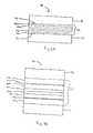
- FIG. 1illustrates a semiconductor material including a compositionally-graded transition layer according to one embodiment of the present invention.
- FIGS. 2A to 2 Iare exemplary profiles of the concentration of an element as a function of the thickness across the compositionally-graded transition layer.
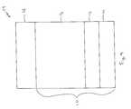
- FIGS. 3A and 3Billustrate a semiconductor material that includes a superlattice transition layer according to another embodiment of the present invention.
- FIGS. 4A and 4Bare exemplary profiles of the concentration of an element as a function of the thickness of the transition layers in the semiconductor materials of FIGS. 3A and 3B, respectively.
- FIG. 5illustrates a textured substrate used to form the semiconductor material according to one embodiment of the present invention.
- FIG. 6illustrates a semiconductor material including an intermediate layer between the substrate and the transition layer according to another embodiment of the present invention.
- FIG. 7illustrates an LED formed from the semiconductor material according to another embodiment of the present invention.
- FIG. 8illustrates a laser diode formed from the semiconductor material according to another embodiment of the present invention.
- FIG. 9illustrates a FET formed from the semiconductor material according to another embodiment of the present invention.
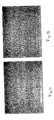
- FIG. 10is a micrograph of the surface of a gallium nitride layer formed on a silicon substrate with a transition layer as described in Example 1.
- FIG. 11is a micrograph of the surface of a gallium nitride layer formed on a silicon substrate without a transition layer as described in comparative Example 2.
- the inventionprovides semiconductor materials including a gallium nitride material layer and a process to produce the semiconductor materials.
- gallium nitride materialrefers to gallium nitride and any of its alloys, such as aluminum gallium nitride (Al x Ga (1-x) N), indium gallium nitride (In y Ga (1-y) N), aluminum indium gallium nitride (Al x In y Ga (1-x-y) N), gallium arsenide phosporide nitride (GaAs s P b N (1-a-b) ), aluminum indium gallium arsenide phosporide nitride (Al x In y Ga (1-x-y) As a P b N (1-a-b) ), amongst others.
- arsenic and/or phosphorousare at low concentrations (i.e., less than 5 weight percent).
- Semiconductor material 10includes a transition layer 12 formed over a silicon substrate 14 and a gallium nitride material layer 16 formed over the transition layer.
- transition layer 12is compositionally-graded to reduce internal stresses within gallium nitride material layer 16 that can result from differences between the thermal expansion rates of substrate 14 and the gallium nitride material layer.
- the internal stressesmay arise, for example, when semiconductor material 10 is cooled after the deposition of gallium nitride material layer 16 and substrate 14 contracts more rapidly than the gallium nitride material layer.
- gallium nitride material layer 16can be formed with a low crack level making semiconductor material 10 suitable for use in a number of applications including FETs, LEDs, laser diodes, and the like.
- compositionally-graded layerrefers to a layer having a composition that varies across at least a portion of the thickness of the layer.
- transition layer 12includes at least two different compositions at different depths within the layer.
- the composition of transition layer 12can be varied in a number of ways. It is generally advantageous to vary the composition of transition layer 12 in a manner that provides sufficient strain relief to limit or prevent the formation of cracks in gallium nitride material layer 16 .
- transition layer 12is composed of an alloy of gallium nitride such as Al x In y Ga (1-x-y) )N, Al x Ga (1-x) N, and In y Ga (1-y) N. It should be understood, however, that transition layers having other compositions may also be used. In embodiments which utilize alloys of gallium nitride, the concentration of at least one of the elements (e.g., Ga, Al, In) of the alloy is typically varied across at least a portion of the thickness of the transition layer. When transition layer 12 has an Al x In y Ga (1-x-y) N composition, x and/or y is varied. When transition layer 12 has a Al x Ga (1-x) N composition, x is varied. When transition layer 12 has a In y Ga (1-y) N composition, y is varied.
- transition layer 12it is desirable for transition layer 12 to have a low gallium concentration at back surface 18 and a high gallium concentration at front surface 20 . It has been found that such transition layers are particularly effective in relieving internal stresses within gallium nitride material layer 16 . Decreasing the gallium concentration of a gallium nitride alloy transition layer can make the thermal expansion rate of the alloy more similar to the thermal expansion rate of silicon. As described further below, gallium nitride material layer 16 typically includes a high gallium concentration. Thus, in these embodiments, increasing the concentration of gallium in transition layer 12 can make the thermal expansion rate of the alloy more similar to the thermal expansion rate of gallium nitride material layer 16 . It is believed that in these preferred embodiments effective strain relief is achievable because back surface 18 has a relatively similar thermal expansion rate as substrate 14 , while front surface 20 has a relatively similar thermal expansion rate as gallium nitride material Layer 16 .
- transition layer 12 at front surface 20it may be preferable for the composition of transition layer 12 at front surface 20 to be the same as the composition of gallium nitride material layer 16 . In some cases, transition layer 12 is free of gallium at back surface 18 and has a composition of GaN at front surface 20 .
- transition layer 12may comprise Al x Ga (1-x) N.
- the transition layeris free of indium.
- transition layer 12may include a small amount of indium, for example, less than 10 percent by weight.
- indiumis present in transition layer 12 (i.e., Al x In y Ga (1-x-y) N)
- the concentration of indiumi.e., y
- the concentration of gallium and aluminummay remain constant throughout the transition layer, while the concentration of gallium and aluminum are graded.
- the composition in transition layer 12may be graded across its thickness in a number of different manners.
- the compositionmay be graded continuously, discontinuously, across the entire thickness, or across only a portion of the thickness.
- the compositionmay be graded by varying the concentration of one or more of the elements (i.e., Ga, Al, In).
- FIGS. 2A to 2 Iillustrate exemplary manners in which the composition may be graded by varying the concentration of one of the elements as a function of thickness across transition layer 12 .
- the profilesrepresent the concentration of gallium across the thickness of transition layer 12 , though it should be understood that in other embodiments the profiles may represent the concentration of other elements (i.e., Al or In).
- FIG. 2Ashows a step-wise variation of concentration as a function of thickness which includes multiple steps.
- FIG. 2Bshows a step-wise variation of concentration as a function of thickness which includes two steps.
- FIG. 2Cshows a saw tooth variation of concentration as a function of thickness.
- FIG. 2Dshows continuous variations of concentration at a constant rate as a function of thickness.
- FIG. 2Eshows a continuous variation of concentration at a constant rate starting from a non-zero concentration.
- FIGS. 2F and 2Gshow continuous variations of concentration as a function of thickness at exponential rates.
- FIG. 2Hshows a discontinuous variation of concentration as a function of thickness.
- FIG. 2Ishows a variation of the concentration across a portion of the thickness of the transition layer.
- transition layer 12may be a compositionally-graded strained layer superlattice 22 according to another embodiment of the present invention.
- Superlattice 22includes alternating layers 24 a , 24 b of semiconductor compounds having different compositions.
- the composition across each individual layer 24 a , 24 bis varied according to any of the manners described above.
- the composition of individual layers 24 a , 24 bis constant across the thickness of the individual layer as shown in the concentration profile of FIGS. 4A and 4B.
- the thicknesses of individual layers 24 a , 24 bis varied across transition layer 12 to provide compositional grading.
- superlattice 22comprises alternating layers of gallium nitride alloys having different compositions.
- layer 24 ahas a composition of Al x In y Ga (1-x-y) N and layer 24 b has a composition of Al a In b Ga (1-a-b) N, wherein x ⁇ a and y ⁇ b.
- concentration of at least one of the elements (i.e., Al, In, Ga) of the alloycan be varied according to any of the manners described above.
- the gallium concentrationis typically different in individual layers 24 a , 24 b.
- the gallium concentration at back surface 18 and a high gallium concentration at front surface 20may be desirable to have a low gallium concentration at back surface 18 and a high gallium concentration at front surface 20 .
- increasing the gallium concentration in a direction away from back surface 18can be accomplished by varying the thickness of individual layers.
- layer 24 ahas a low gallium concentration and layer 24 b has a high gallium concentration.
- layers 24 aare relatively thick and layers 24 b are relatively thin proximate back surface 18 .
- the thickness of layers 24 ais decreased and the thickness of layers 24 b is increased in a direction away from back surface 18 .
- layers 24 aare relatively thin and layers 24 b are relatively thick proximate front surface 20 .
- This structureprovides a low gallium concentration at back surface 18 and a high gallium concentration at front surface 20 .
- transition layer 12may be formed of a combination of a single layer having a graded composition and a superlattice.
- the superlatticeis formed over the single compositionally-graded layer.
- the single compositionally-graded layeris formed over the superlattice.
- Transition layer 12can have a variety of thicknesses depending on the application. Generally, though not always, transition layer 12 has a thickness of less than about 500 microns. In some cases, relatively thick transition layers are preferable, for example between about 2.0 microns and about 20 microns. Thick transition layers may be preferred when thick gallium nitride material layers (i.e., greater than 5 microns) are produced. In some cases, relatively thin transition layers are preferable, for example between about 0.03 micron and about 2.0 microns. When superlattice structures are used as transition layers, the thickness of individual layers 24 a , 24 b depends upon the particular application. Typically the thickness of individual layers 24 a , 24 b may be between about 0.001 microns and about 0.020 microns. As described above, the thicknesses of individual layers may vary across transition layer 12 (FIG. 3B).
- Gallium nitride material layer 16is formed of gallium nitride (GaN) or any of its alloys including aluminum gallium nitride (Al x Ga (1-x) N), indium gallium nitride (In y Ga (1-y) N), and aluminum indium gallium nitride (Al x In y Ga (1-x-y) N).
- the composition of gallium nitride material layer 16is generally constant across its thickness as distinguished with transition layer 12 .
- x and/or yare generally fixed when gallium nitride material is formed of any of the aforementioned compound alloys. It should be understood that small variations in the composition of gallium nitride material layer 16 may occur, for example, as a result of slight non-uniformities and inhomogeneities during growth.
- gallium nitride material layer 16has a low crack level as a result of the ability of transition layer 12 to relieve stress arising from differences in thermal expansion rates between the silicon substrate and the gallium nitride material.
- a “crack,” as used herein,is a linear fracture or a cleavage having a length to width ratio of greater than 5:1 that extends to the surface of the gallium nitride material. It should be understood that a crack may or may not extend through the entire thickness of the gallium nitride material.
- “Crack level”is defined as a total measure of all crack lengths in a gallium nitride material per unit surface area. Crack level can be expressed in units of ⁇ m/ ⁇ m 2 .
- the crack level of a gallium nitride materialcan be measured, for example, using optical microscopy techniques. To determine the crack level, the length of all of the cracks in a given area (i.e., 1 mm ⁇ 1 mm) are added together and divided by the total surface area. If necessary, this process may be repeated at a number of locations across the surface to provide a measurement representative of the entire gallium nitride material. The crack level at each location may be averaged to provide a crack level for the material. The number of locations depends upon the amount of surface area of the gallium nitride material. When measuring the crack level of a gallium nitride material, measurements are not made within a region proximate to edges of the material known as an edge exclusion. The nominal edge exclusion is 5 mm from the edge. Edge effects in such regions may lead to increased crack levels and are typically not used to in device formation.
- Gallium nitride material layer 16advantageously has a low crack level. In some cases, gallium nitride material layer 16 has a crack level of less than 0.005 ⁇ m/ ⁇ m . In some cases, gallium nitride material has a very low crack level of less than 0.001 ⁇ m/ ⁇ m. In certain cases, it may be preferable for gallium nitride material layer 16 to be substantially crack-free as defined by a crack level of less than 0.0001 ⁇ m/ ⁇ m 2 .
- Gallium nitride material layer 16preferably has a monocrystalline structure. In preferred cases, gallium nitride material layer 16 has a Wurtzite (hexagonal) structure. Preferably, the entire gallium nitride material layer has a Wurtzite structure.
- the gallium nitride material layer 16is generally of high enough quality so as to permit the formation of devices therein. In some embodiments, gallium nitride material layer 16 has a relatively low amount of defects (e.g., less than 10 9 cm ⁇ 2 ) which, for example, result from the lattice mismatch between gallium nitride and silicon.
- gallium nitride material layer 16is dictated, in part, by the requirements of the specific application. In applications when gallium nitride material is used as a device layer, the thickness is sufficient to permit formation of the device.
- Gallium nitride material layer 16generally has a thickness of greater than 0.1 micron, though not always. In other cases, thicker gallium nitride material layers are desired such as thicknesses greater than 0.5 micron, greater than 0.75 micron, greater than 1.0 microns, greater than 2.0 microns, or even greater than 5.0 microns. Even thick gallium nitride material layers 16 are achievable at low crack densities because of the presence of transition layer 12 .
- upper regions of the layermay include low amounts of defects due to the tendency of defects to annihilate one another as they propagate vertically through the layer.
- the use of thick gallium nitride layersmay improve device performance.
- Silicon substrate 14typically is formed of high-quality single-crystal silicon as readily available in the art. Silicon substrates 14 having different crystallographic orientations may be used. In some cases, silicon ( 111 ) substrates are preferred. In other cases, silicon ( 100 ) substrates are preferred. Gallium nitride material layer 16 having a Wurtzite structure may be grown on silicon ( 111 ) substrates and silicon ( 100 ) substrates using transition layer 12 .
- gallium nitride material layer 16 having a Wurtzite structuremay grown on silicon ( 100 ) substrates because conventional techniques generally result in gallium nitride materials having a mixture of zinc blend (cubic) and Wurtzite structures when grown on silicon ( 100 ) substrates.
- Silicon substratemay have any dimensions as used in the art. Suitable diameters include, but are not limited to, 2 inches, 4 inches, 6 inches, and 8 inches. In some embodiments, silicon substrate 14 is relatively thick, for example, greater than 250 microns. Thicker substrates are generally able to resist bending which can occur, in some cases, in thinner substrates.
- silicon substrate 14refers to any substrate that includes a silicon layer at its top surface.
- suitable silicon substratesinclude substrates that are composed entirely of silicon (e.g., silicon wafers), silicon-on-insulator (SOI) substrates, silicon-on-sapphire substrate (SOS), SIMOX substrates, amongst others.
- silicon substrate 14is textured according to some embodiments of the present invention.
- textured substrate 14includes a plurality of posts 24 which define trenches 26 therebetween.
- Such texturingcan be provided using selective etching and/or selective epitaxial growth. Etching may be performed using standard dry or wet etching techniques, such as with a mask which later may be removed.
- textured substratesare used in conjunction with the transition layers described herein to grow gallium nitride material layers with very low defect densities (e.g., less than 10 7 cm ⁇ 2 ).
- Silicon substrate 14may also be pre-patterned to include mask areas which selectively expose regions of the substrate, while covering other regions. Such pre-patterned substrates enable selective area epitaxial growth which may be advantageous in minimizing defect densities.
- semiconductor material 10includes an intermediate layer 28 between silicon substrate 14 and transition layer 12 according to another embodiment of the present invention. It should be understood that intermediate layer 28 may also be positioned between transition layer 12 and gallium nitride material layer 16 . Intermediate layer 28 , when provided, may further relieve stress in gallium nitride material layer 16 . Intermediate layer generally has a thickness of less than about 500 microns and, in some cases, between about 0.01 micron and about 2.0 microns. The presence of intermediate layer 28 may permit reduction of the thickness of transition layer 12 . The composition of the intermediate layer is generally constant throughout its thickness.
- Intermediate layer 28can be composed of a GaN alloy such as aluminum gallium nitride (Al x Ga (1-x) N), indium gallium nitride (In y Ga (1-y) N), and aluminum indium gallium nitride (Al x In y Ga (1-x-y) N).
- Al x Ga (1-x) Naluminum gallium nitride
- In y Ga (1-y) Nindium gallium nitride
- Al x In y Ga (1-x-y) Naluminum indium gallium nitride
- Al x In y Ga (1-x-y) Naluminum indium gallium nitride
- the sum of (x+y) in the intermediate layermay be greater than 0.4, greater than 0.6, greater than 0.8, greater than 0.9, or even more.
- the intermediate layeris free of gallium and is composed of Al x In y N or AlN.
- GaN alloy intermediate layers with low Ga concentrationsmay be effective at
- intermediate layer 28may be utilized in accordance with any of the embodiments described herein including embodiments that use a superlattice as a transition layer.
- transition layer 12includes a single compositionally-graded layer and a superlattice
- the intermediate layermay be positioned between the compositionally-graded layer and the superlattice.
- more than one intermediate layer 28 having different compositionsmay be provided.
- transition layer 12 and gallium nitride material layer 16are grown using a metalorganic chemical vapor deposition (MOCVD) process. It should be understood that other suitable techniques known in the art may also be utilized to deposit transition layer 12 and gallium nitride material layer 16 including molecular beam epitaxy (MBE), hydride vapor phase epitaxy (HVPE), and the like.
- MOCVDmetalorganic chemical vapor deposition
- the MOCVD processinvolves introducing different source gases into an environment (e.g., a process system) around a substrate and providing conditions which promote a reaction between the gases to form a layer on the substrate surface.
- the reactionproceeds until a layer of desired thickness is achieved.
- the composition of the layermay be controlled, as described further below, by several factors including gas composition, gas concentration, and the reaction conditions (e.g. temperature and pressure).
- Examples of suitable source gases for MOCVD growth of the transition layerinclude trimethylaluminum (TMA) or triethylaluminum (TEA) as sources of aluminum; trimethylindium (TMI) or triethylindium (TEI) as sources of indium; trimethylgallium (TMG) or trimethylgallium (TEG) as sources of gallium; and ammonia (NH 3 ) as a source of nitrogen.
- TMAtrimethylaluminum
- TMAtriethylaluminum
- TEItriethylindium
- TMGtrimethylgallium
- TEGtrimethylgallium
- NH 3ammonia
- the particular source gas useddepends upon the desired composition of the transition layer.
- an aluminum sourcee.g., TMA or TEA
- TMG or TEGgallium source
- a nitrogen sourceare used to deposit films having an Al x Ga 1-x N composition.
- the flow rates of the source gases, the ratios of the source gases, and the absolute concentrations of the source gasesmay be controlled to provide transition layers having the desired composition.
- typical TMA flow ratesare between about 5 ⁇ mol/min and about 50 ⁇ mol/min with a flow rate of about 20 ⁇ mol/min being preferred in some cases;
- typical TMG flow ratesare between about 5 ⁇ mol/min and 250 ⁇ mol/min, with a flow rate of 115 ⁇ mol/min being preferred in some cases;
- the flow rate of ammoniais typically between about 3 slpm to about 10 slpm.
- the reaction temperaturesare generally between about 900° C. and about 1200° C. and the process pressures are between about 1 Torr and about 760 Torr. It is to be understood that the process conditions, and in particular the flow rate, are highly dependent on the process system configuration. Typically, smaller throughput systems require less flow than larger throughput systems.
- Process parametersare suitably adjusted to control the compositional grading of the transition layer.
- the compositionmay be graded by changing the process conditions to favor the growth of particular compositions. For example, to increase incorporation of gallium in the transition layer thereby increasing the gallium concentration, the flow rate and/or the concentration of the gallium source (e.g., TMG or TEG) may be increased. Similarly, to increase incorporation of aluminum into the transition layer thereby increasing the aluminum concentration, the flow rate and/or the concentration of the aluminum source (e.g., TMA or TEA) may be increased. The manner in which the flow rate and/or the concentration of the source is increased (or decreased) controls the manner in which the composition is graded.
- the flow rate and/or the concentration of the sourcecontrols the manner in which the composition is graded.
- the temperature and/or pressureis adjusted to favor the growth of a particular compound. Growth temperatures and pressures favoring the incorporation of gallium into the transition layer differ from the growth temperatures and pressures favoring the incorporation of aluminum into the transition layer.
- the compositionmay be graded by suitably adjusting temperature and pressure.
- Typical growth rates of the transition layerare between about 0.01 ⁇ m/hr and about 3.0 ⁇ m/hr. The growth rate depends upon the process parameters as well as the composition of the layer.
- the gallium nitride material layer(and intermediate layers, if present) may also be grown using an MOCVD process.
- the processmay utilize source gases and process parameters similar to those described above for the deposition of the transition layer. The particular source gases and process parameters are selected based upon the desired composition. When depositing the gallium nitride material layer (or the intermediate layer), however, the process parameters are maintained constant so as to provide a film having a constant composition.
- semiconductor materials of the inventionmay be used in a variety of applications.
- semiconductor material 10is processed using known techniques to form a semiconductor device. Doped regions may be formed within gallium nitride material layer 16 and additional layers may be deposited upon the gallium nitride material layer to produce the desired semiconductor structure.
- gallium nitride material layer 16is doped using known techniques to achieve a desired conductivity.
- Any suitable semiconductor device known in the art including electronic and optical devicescan be produced using semiconductor material 10 .
- Exemplary devicesinclude LEDs, laser diodes, FETs (e.g., HFETs) amongst others.
- FIG. 7schematically illustrates an exemplary LED 30 formed from semiconductor material 10 .
- LED 30includes silicon-doped gallium nitride material layer 16 formed on transition layer 12 on silicon substrate 14 .
- the following layersare formed on gallium nitride material layer 16 in succession: a silicon-doped Al x Ga (1-x) N layer 31 (containing 0-20% by weight Al), a GaN/InGaN single or multiple quantum well 32 , a magnesium-doped Al x Ga (1-x) N layer 34 (containing 10-20% by weight Al), and a magnesium-doped GaN layer 36 .
- LED 30includes a p-type metal contact 38 on magnesium-doped GaN layer 36 and an n-type metal contact pad 39 on silicon-doped gallium nitride material layer 16 .
- FIG. 8schematically illustrates an exemplary laser diode 40 formed from semiconductor material 10 .
- Laser diode 40includes silicon-doped gallium nitride material layer 16 formed on transition layer 12 on silicon substrate 14 .
- the following layersare formed on gallium nitride material layer 16 in succession: a silicon-doped Al x Ga (1-x) N layer 42 (containing 5-30% by weight Al), a silicon-doped Al x Ga (1-x) N layer 44 (containing 0-20% by weight Al), a GaN/InGaN single or multiple quantum well 46 , a magnesium-doped Al x Ga (1-x) N layer 48 (containing 5-20% by weight Al), a magnesium-doped Al x Ga (1-x) N layer 50 (containing 5-30% by weight Al), and a magnesium-doped GaN layer 52 .
- Laser diode 40includes a p-type metal contact 38 on magnesium-doped GaN layer 52 and an n-type metal contact pad 39 on silicon-doped gallium nitride material layer 16 . It should be understood that laser diode 40 may have a variety of different structures as known to those of ordinary skill in the art.
- FIG. 9schematically illustrates a FET 54 (e.g., HFET) formed from semiconductor material 10 .
- FET 54includes intrinsic gallium nitride material layer 16 formed on transition layer 12 on silicon substrate 14 .
- FET 54includes an Al x Ga (1-x) N layer 56 (containing 10-40% by weight Al). It should be understood that FET 54 may have a variety of different structures as known to those of ordinary skill in the art.
- This exampleillustrates the effectiveness of a compositionally-graded transition layer in limiting the number of cracks in a gallium nitride material grown on a silicon substrate.
- An MOCVD processwas used to grow an AlN intermediate layer, an Al x Ga 1-x N compositionally-graded transition layer, and a GaN layer in succession on a silicon substrate.
- a silicon substrate having a 2-inch diameter and a thickness of 250 micronswas positioned in an MOCVD system.
- TMAtrimethylaluminum gas
- NH 3ammonia gas
- a growth temperature of between about 1000-1100° C. and a growth pressure 30-200 Torrwere maintained in the system.
- an AlN intermediate layerwas formed having a thickness of about 0.3 micron on the silicon substrate.
- TMGtrimethylgallium
- the introduction of TMA into the systemwas stopped and the TMG flow rate was adjusted to about 115 ⁇ mol/min.
- the flow rate of ammoniawas maintained between about 3 and about 10 slpm.
- the growth temperaturewas maintained between about 1000 and about 1050° C. and the growth pressure between about 30 and about 200 Torr.
- a GaN layer having a thickness of about 1.5 micronwas grown on the compositionally-graded transition layer.
- the semiconductor materialwas furnace-cooled to room temperature and removed from the MOCVD system for analysis.
- the resulting semiconductor materialincluded a 0.3 micron AlN intermediate layer formed on the silicon substrate; a 0.4 micron thick continuously graded Al x Ga 1-x N transition layer formed on the intermediate layer; and a 1.5 micron GaN layer grown on the transition layer.
- the GaN layerhad a monocrystalline structure.
- the crack level of the semiconductor materialwas measured using an optical microscopic technique.
- the microscopewas equipped with the camera capable of taking micrographs of the surface of the GaN layer.
- FIG. 10is a micrograph showing a representative area of slightly greater than 1 mm 2 on the surface of the GaN layer. No cracks are visible in the representative area. Measurements were repeated at several other locations on the surface of the GaN layer and similar results were achieved.
- the gallium nitride materialwas found to be substantially crack-free as defined by a crack level of less than 0.0001 ⁇ m/ ⁇ m 2 .
- This exampleillustrates the ability to grow gallium nitride layers having a low crack level on a silicon substrate using a compositionally-graded transition layer.
- This exampleillustrates the generation of cracks in a gallium nitride material grown on a silicon substrate without using a compositionally-graded transition layer.
- An MOCVD processwas used to grow an AlN intermediate layer and a GaN layer in succession on a silicon substrate.
- a silicon ( 111 ) substrate having a 2-inch diameter and a thickness of 250 micronswas positioned in the same MOCVD system as used in Example 1.
- An AlN intermediate layerwas formed using essentially the same processing conditions as the growth of the intermediate layer in Example 1.
- a GaN layerwas grown on the intermediate layer using essentially the same processing conditions as the growth of the GaN layer in Example 1.
- a compositionally-graded transition layerwas not grown.
- the semiconductor materialwas furnace-cooled to room temperature and removed from the MOCVD system for analysis.
- the resulting semiconductor materialincluded a 0.3 micron AlN intermediate layer formed on the silicon substrate, and a 1.5 micron GaN layer grown on the intermediate layer.
- the GaN layerhad a monocrystalline structure.
- FIG. 11is a micrograph showing a representative area of slightly greater than 1 mm 2 on the surface of the GaN layer. The length of each crack in the area was measured and added together to determine the total crack length. The total crack length was divided by the surface area to determine the crack level. Measurements were repeated at several other locations on the surface which were averaged to provide a crack level of the GaN layer of about 0.007 ⁇ m/ ⁇ m.
- This comparative exampleillustrates the presence of cracks in gallium nitride layers grown on a silicon substrate without using a compositionally-graded transition layer.
Landscapes
- Engineering & Computer Science (AREA)
- Chemical & Material Sciences (AREA)
- Microelectronics & Electronic Packaging (AREA)
- Power Engineering (AREA)
- Physics & Mathematics (AREA)
- Condensed Matter Physics & Semiconductors (AREA)
- General Physics & Mathematics (AREA)
- Manufacturing & Machinery (AREA)
- Computer Hardware Design (AREA)
- Crystallography & Structural Chemistry (AREA)
- Materials Engineering (AREA)
- Organic Chemistry (AREA)
- Metallurgy (AREA)
- Chemical Kinetics & Catalysis (AREA)
- General Chemical & Material Sciences (AREA)
- Inorganic Chemistry (AREA)
- Led Devices (AREA)
- Physical Vapour Deposition (AREA)
- Semiconductor Lasers (AREA)
- Ceramic Products (AREA)
- Crystals, And After-Treatments Of Crystals (AREA)
- Chemical Vapour Deposition (AREA)
Abstract
Description
- The invention relates generally to semiconductor materials and, more particularly, to gallium nitride materials and methods of producing gallium nitride materials.[0001]
- Gallium nitride materials include gallium nitride (GaN) and its alloys such as aluminum gallium nitride (AlGaN), indium gallium nitride (InGaN), and aluminum indium gallium nitride (AlInGaN). These materials are semiconductor compounds that have a relatively wide, direct bandgap which permits highly energetic electronic transitions to occur. Such electronic transitions can result in gallium nitride materials having a number of attractive properties including the ability to efficiently emit blue light, the ability to transmit signals at high frequency, and others. Accordingly, gallium nitride materials are being widely investigated in many microelectronic applications such as transistors, field emitters, and optoelectronic devices.[0002]
- In many applications, gallium nitride materials are grown on a substrate. However, differences in the properties between gallium nitride materials and substrates can lead to difficulties in growing layers suitable for many applications. For example, gallium nitride (GaN) has a different thermal expansion coefficient (i.e., thermal expansion rate) than many substrate materials including sapphire, silicon carbide, and silicon. This difference in thermal expansion can lead to cracking of a gallium nitride layer deposited on such substrates when the structure is cooled, for example, during processing. The cracking phenomena can prevent gallium nitride materials from being suitable for use in many applications. Cracking can be particularly problematic for relatively thick (e.g., >0.5 micron) gallium nitride layers.[0003]
- Gallium nitride (GaN) also has a different lattice constant than most substrate materials. The difference in lattice constant may lead to the formation of defects in gallium nitride material layers deposited on substrates. Such defects can impair the performance of devices formed using the gallium nitride material layers.[0004]
- Prior art techniques have been developed to address crack formation and defect formation in gallium nitride materials deposited on sapphire substrates and silicon carbide substrates. Such techniques, for example, may involve depositing one or more buffer layers on the substrate and, then, depositing the gallium nitride material on the buffer layer(s).[0005]
- The invention provides semiconductor materials including a gallium nitride material layer formed on a silicon substrate and methods to form the semiconductor materials. The semiconductor materials include a transition layer formed between the silicon substrate and the gallium nitride material layer. The transition layer is compositionally-graded to lower stresses in the gallium nitride material layer which can result from differences in thermal expansion rates between the gallium nitride material and the substrate. The lowering of stresses in the gallium nitride material layer reduces the tendency of cracks to form which enables the production of semiconductor materials including gallium nitride material layers having few or no cracks. The semiconductor materials may be used in a number of microelectronic and optical applications.[0006]
- The invention has overcome the problem of growing gallium nitride materials having few or no cracks on silicon substrates which, due to the large differences in both thermal expansion rate and lattice constant between gallium nitride materials (e.g., GaN) and silicon, is considerably more challenging than on other types of substrates (e.g., SiC and sapphire).[0007]
- In one aspect, the invention provides a semiconductor material. The material includes a silicon substrate and a compositionally-graded transition layer formed over the silicon substrate. The material further includes a gallium nitride material layer formed over the transition layer.[0008]
- In another aspect, the invention provides a semiconductor material. The semiconductor material includes a silicon substrate and a gallium nitride material layer formed over the silicon substrate. The gallium nitride material layer has a crack level of less than 0.005 μm/μm[0009]2.
- In another aspect, the invention provides a semiconductor structure. The semiconductor structure includes a silicon substrate, and a gallium nitride material layer formed over the silicon substrate. The gallium nitride material layer has a thickness of greater than 0.5 micron. The semiconductor structure forms a semiconductor device.[0010]
- In another aspect, the invention provides a method of producing a semiconductor material. The method includes the steps of forming a compositionally-graded transition layer over a silicon substrate, and forming a gallium nitride material layer over the transition layer.[0011]
- In another aspect, the invention provides a method of producing a semiconductor material. The method includes forming a gallium nitride material layer formed over a silicon substrate. The gallium nitride material layer has a crack level of less than 0.005 μm/μm[0012]2.
- In another aspect, the invention provides a method of forming a semiconductor structure. The method includes forming a semiconductor structure comprising a silicon substrate, and a gallium nitride material layer formed over the silicon substrate. The gallium nitride material layer has a thickness of greater than 0.5 micron.[0013]
- In another aspect, the invention provides a semiconductor material. The semiconductor material comprises a silicon ([0014]100) substrate and a gallium nitride material layer having a Wurtzite structure formed over the silicon substrate.
- Other advantages, aspects, and features of the invention will become apparent from the following detailed description of the invention when considered in conjunction with the accompanying drawings.[0015]
- FIG. 1 illustrates a semiconductor material including a compositionally-graded transition layer according to one embodiment of the present invention.[0016]
- FIGS. 2A to[0017]2I are exemplary profiles of the concentration of an element as a function of the thickness across the compositionally-graded transition layer.
- FIGS. 3A and 3B illustrate a semiconductor material that includes a superlattice transition layer according to another embodiment of the present invention.[0018]
- FIGS. 4A and 4B are exemplary profiles of the concentration of an element as a function of the thickness of the transition layers in the semiconductor materials of FIGS. 3A and 3B, respectively.[0019]
- FIG. 5 illustrates a textured substrate used to form the semiconductor material according to one embodiment of the present invention.[0020]
- FIG. 6 illustrates a semiconductor material including an intermediate layer between the substrate and the transition layer according to another embodiment of the present invention.[0021]
- FIG. 7 illustrates an LED formed from the semiconductor material according to another embodiment of the present invention.[0022]
- FIG. 8 illustrates a laser diode formed from the semiconductor material according to another embodiment of the present invention.[0023]
- FIG. 9 illustrates a FET formed from the semiconductor material according to another embodiment of the present invention.[0024]
- FIG. 10 is a micrograph of the surface of a gallium nitride layer formed on a silicon substrate with a transition layer as described in Example 1.[0025]
- FIG. 11 is a micrograph of the surface of a gallium nitride layer formed on a silicon substrate without a transition layer as described in comparative Example 2.[0026]
- The invention provides semiconductor materials including a gallium nitride material layer and a process to produce the semiconductor materials. As used herein, the phrase “gallium nitride material” refers to gallium nitride and any of its alloys, such as aluminum gallium nitride (Al[0027]xGa(1-x)N), indium gallium nitride (InyGa(1-y)N), aluminum indium gallium nitride (AlxInyGa(1-x-y)N), gallium arsenide phosporide nitride (GaAssPbN(1-a-b)), aluminum indium gallium arsenide phosporide nitride (AlxInyGa(1-x-y)AsaPbN(1-a-b)), amongst others. Typically, when present, arsenic and/or phosphorous are at low concentrations (i.e., less than 5 weight percent).
- Referring to FIG. 1, a[0028]
semiconductor material 10 according to one embodiment of the invention is shown.Semiconductor material 10 includes atransition layer 12 formed over asilicon substrate 14 and a galliumnitride material layer 16 formed over the transition layer. As described further below,transition layer 12 is compositionally-graded to reduce internal stresses within galliumnitride material layer 16 that can result from differences between the thermal expansion rates ofsubstrate 14 and the gallium nitride material layer. The internal stresses may arise, for example, whensemiconductor material 10 is cooled after the deposition of galliumnitride material layer 16 andsubstrate 14 contracts more rapidly than the gallium nitride material layer. As a result of the reduced internal stresses, galliumnitride material layer 16 can be formed with a low crack level makingsemiconductor material 10 suitable for use in a number of applications including FETs, LEDs, laser diodes, and the like. - It should be understood that when a layer is referred to as being “on” or “over” another layer or substrate, it can be directly on the layer or substrate, or an intervening layer may also be present. It should also be understood that when a layer is referred to as being “on” or “over” another layer or substrate, it may cover the entire layer or substrate, or a portion of the layer or substrate.[0029]
- As used herein, the term “compositionally-graded layer” refers to a layer having a composition that varies across at least a portion of the thickness of the layer. Thus,[0030]
transition layer 12 includes at least two different compositions at different depths within the layer. As described further below, the composition oftransition layer 12 can be varied in a number of ways. It is generally advantageous to vary the composition oftransition layer 12 in a manner that provides sufficient strain relief to limit or prevent the formation of cracks in galliumnitride material layer 16. - According to one set of embodiments,[0031]
transition layer 12 is composed of an alloy of gallium nitride such as AlxInyGa(1-x-y))N, AlxGa(1-x)N, and InyGa(1-y)N. It should be understood, however, that transition layers having other compositions may also be used. In embodiments which utilize alloys of gallium nitride, the concentration of at least one of the elements (e.g., Ga, Al, In) of the alloy is typically varied across at least a portion of the thickness of the transition layer. Whentransition layer 12 has an AlxInyGa(1-x-y)N composition, x and/or y is varied. Whentransition layer 12 has a AlxGa(1-x)N composition, x is varied. Whentransition layer 12 has a InyGa(1-y)N composition, y is varied. - In certain preferred embodiments, it is desirable for[0032]
transition layer 12 to have a low gallium concentration at backsurface 18 and a high gallium concentration atfront surface 20. It has been found that such transition layers are particularly effective in relieving internal stresses within galliumnitride material layer 16. Decreasing the gallium concentration of a gallium nitride alloy transition layer can make the thermal expansion rate of the alloy more similar to the thermal expansion rate of silicon. As described further below, galliumnitride material layer 16 typically includes a high gallium concentration. Thus, in these embodiments, increasing the concentration of gallium intransition layer 12 can make the thermal expansion rate of the alloy more similar to the thermal expansion rate of galliumnitride material layer 16. It is believed that in these preferred embodiments effective strain relief is achievable becauseback surface 18 has a relatively similar thermal expansion rate assubstrate 14, whilefront surface 20 has a relatively similar thermal expansion rate as galliumnitride material Layer 16. - In some cases, the sum of (x+y) at[0033]
back surface 18 is greater than 0.4, greater than 0.6, greater than 0.8 or ever higher. In some preferred embodiments, (x+y)=1 atback surface 18, so thattransition layer 12 is free of gallium at the back surface. In some cases, the sum of (x+y) is less than 0.3, less than 0.2, or even less atfront surface 20. In some preferred embodiments, the sum of (x+y)=0 atfront surface 20, so thattransition layer 12 has a composition of GaN at the front surface. It may be particularly preferred fortransition layer 12 to have a composition of GaN atfront surface 20, when galliumnitride material layer 16 has a composition of GaN. In other cases when gallium nitride material layer is composed of an alloy of GaN, it may be preferable for the composition oftransition layer 12 atfront surface 20 to be the same as the composition of galliumnitride material layer 16. In some cases,transition layer 12 is free of gallium at backsurface 18 and has a composition of GaN atfront surface 20. - In certain embodiments, it may be preferable for[0034]
transition layer 12 to comprise AlxGa(1-x)N. In these cases, the transition layer is free of indium. In other cases,transition layer 12 may include a small amount of indium, for example, less than 10 percent by weight. When indium is present in transition layer12 (i.e., AlxInyGa(1-x-y)N), the concentration of indium (i.e., y) may remain constant throughout the transition layer, while the concentration of gallium and aluminum are graded. - The composition in[0035]
transition layer 12 may be graded across its thickness in a number of different manners. For example, the composition may be graded continuously, discontinuously, across the entire thickness, or across only a portion of the thickness. As described above, the composition may be graded by varying the concentration of one or more of the elements (i.e., Ga, Al, In). FIGS. 2A to2I illustrate exemplary manners in which the composition may be graded by varying the concentration of one of the elements as a function of thickness acrosstransition layer 12. In certain preferred embodiments, the profiles represent the concentration of gallium across the thickness oftransition layer 12, though it should be understood that in other embodiments the profiles may represent the concentration of other elements (i.e., Al or In). The convention in FIGS. 2A to2I is that the thickness oftransition layer 12 increases in the direction away from substrate14 (i.e., t=0 atback surface 18 and t=1 at front surface20). - FIG. 2A shows a step-wise variation of concentration as a function of thickness which includes multiple steps. FIG. 2B shows a step-wise variation of concentration as a function of thickness which includes two steps. FIG. 2C shows a saw tooth variation of concentration as a function of thickness. FIG. 2D shows continuous variations of concentration at a constant rate as a function of thickness. FIG. 2E shows a continuous variation of concentration at a constant rate starting from a non-zero concentration. FIGS. 2F and 2G show continuous variations of concentration as a function of thickness at exponential rates. FIG. 2H shows a discontinuous variation of concentration as a function of thickness. FIG. 2I shows a variation of the concentration across a portion of the thickness of the transition layer.[0036]
- It should be understood that the profiles illustrated in FIGS. 2A to[0037]2I are intended to be exemplary and that the composition of
transition layer 12 may be graded in other manners that are within the scope of the present invention. - Referring to FIGS. 3A and 3B,[0038]
transition layer 12 may be a compositionally-gradedstrained layer superlattice 22 according to another embodiment of the present invention.Superlattice 22 includes alternatinglayers individual layer individual layers individual layers transition layer 12 to provide compositional grading. - In one preferred set of embodiments,[0039]
superlattice 22 comprises alternating layers of gallium nitride alloys having different compositions. For example, layer24ahas a composition of AlxInyGa(1-x-y)N andlayer 24bhas a composition of AlaInbGa(1-a-b)N, wherein x≠a and y≠b. In cases when the composition is graded across each individual layer, the concentration of at least one of the elements (i.e., Al, In, Ga) of the alloy can be varied according to any of the manners described above. In cases when the composition ofindividual layers individual layers - As described above, it may be desirable to have a low gallium concentration at back[0040]
surface 18 and a high gallium concentration atfront surface 20. In embodiments that utilizesuperlattice 22 astransition layer 12, increasing the gallium concentration in a direction away fromback surface 18 can be accomplished by varying the thickness of individual layers. As shown in FIGS. 3B and 4B,layer 24ahas a low gallium concentration andlayer 24bhas a high gallium concentration. As shown, layers24aare relatively thick and layers24bare relatively thinproximate back surface 18. The thickness oflayers 24ais decreased and the thickness oflayers 24bis increased in a direction away fromback surface 18. Thus, layers24aare relatively thin and layers24bare relatively thick proximatefront surface 20. This structure provides a low gallium concentration at backsurface 18 and a high gallium concentration atfront surface 20. - It should be understood that[0041]
transition layer 12 may be formed of a combination of a single layer having a graded composition and a superlattice. In some cases, the superlattice is formed over the single compositionally-graded layer. In other cases, the single compositionally-graded layer is formed over the superlattice. - [0042]
Transition layer 12 can have a variety of thicknesses depending on the application. Generally, though not always,transition layer 12 has a thickness of less than about 500 microns. In some cases, relatively thick transition layers are preferable, for example between about 2.0 microns and about 20 microns. Thick transition layers may be preferred when thick gallium nitride material layers (i.e., greater than 5 microns) are produced. In some cases, relatively thin transition layers are preferable, for example between about 0.03 micron and about 2.0 microns. When superlattice structures are used as transition layers, the thickness ofindividual layers individual layers - Gallium[0043]
nitride material layer 16 is formed of gallium nitride (GaN) or any of its alloys including aluminum gallium nitride (AlxGa(1-x)N), indium gallium nitride (InyGa(1-y)N), and aluminum indium gallium nitride (AlxInyGa(1-x-y)N). The composition of galliumnitride material layer 16 is generally constant across its thickness as distinguished withtransition layer 12. Thus, x and/or y are generally fixed when gallium nitride material is formed of any of the aforementioned compound alloys. It should be understood that small variations in the composition of galliumnitride material layer 16 may occur, for example, as a result of slight non-uniformities and inhomogeneities during growth. - In certain preferred embodiments, gallium[0044]
nitride material layer 16 has a high concentration of gallium and includes little or no amounts of aluminum and/or indium. In high gallium concentration embodiments, the sum of (x+y) may be less than 0.4, less than 0.2, less than 0.1, or even less. In some cases, it is preferable for galliumnitride material layer 16 to have a composition of GaN (i.e., x+y=0). - As described above, gallium[0045]
nitride material layer 16 has a low crack level as a result of the ability oftransition layer 12 to relieve stress arising from differences in thermal expansion rates between the silicon substrate and the gallium nitride material. A “crack,” as used herein, is a linear fracture or a cleavage having a length to width ratio of greater than 5:1 that extends to the surface of the gallium nitride material. It should be understood that a crack may or may not extend through the entire thickness of the gallium nitride material. “Crack level” is defined as a total measure of all crack lengths in a gallium nitride material per unit surface area. Crack level can be expressed in units of μm/μm2. The crack level of a gallium nitride material can be measured, for example, using optical microscopy techniques. To determine the crack level, the length of all of the cracks in a given area (i.e., 1 mm×1 mm) are added together and divided by the total surface area. If necessary, this process may be repeated at a number of locations across the surface to provide a measurement representative of the entire gallium nitride material. The crack level at each location may be averaged to provide a crack level for the material. The number of locations depends upon the amount of surface area of the gallium nitride material. When measuring the crack level of a gallium nitride material, measurements are not made within a region proximate to edges of the material known as an edge exclusion. The nominal edge exclusion is 5 mm from the edge. Edge effects in such regions may lead to increased crack levels and are typically not used to in device formation. - Gallium[0046]
nitride material layer 16 advantageously has a low crack level. In some cases, galliumnitride material layer 16 has a crack level of less than 0.005 μm/μm . In some cases, gallium nitride material has a very low crack level of less than 0.001 μm/μm. In certain cases, it may be preferable for galliumnitride material layer 16 to be substantially crack-free as defined by a crack level of less than 0.0001 μm/μm2. - Gallium[0047]
nitride material layer 16 preferably has a monocrystalline structure. In preferred cases, galliumnitride material layer 16 has a Wurtzite (hexagonal) structure. Preferably, the entire gallium nitride material layer has a Wurtzite structure. The galliumnitride material layer 16 is generally of high enough quality so as to permit the formation of devices therein. In some embodiments, galliumnitride material layer 16 has a relatively low amount of defects (e.g., less than 109cm−2) which, for example, result from the lattice mismatch between gallium nitride and silicon. - The thickness of gallium[0048]
nitride material layer 16 is dictated, in part, by the requirements of the specific application. In applications when gallium nitride material is used as a device layer, the thickness is sufficient to permit formation of the device. Galliumnitride material layer 16 generally has a thickness of greater than 0.1 micron, though not always. In other cases, thicker gallium nitride material layers are desired such as thicknesses greater than 0.5 micron, greater than 0.75 micron, greater than 1.0 microns, greater than 2.0 microns, or even greater than 5.0 microns. Even thick gallium nitride material layers16 are achievable at low crack densities because of the presence oftransition layer 12. In relatively thick gallium nitride layers, upper regions of the layer may include low amounts of defects due to the tendency of defects to annihilate one another as they propagate vertically through the layer. Thus, in these cases, the use of thick gallium nitride layers may improve device performance. - [0049]
Silicon substrate 14 typically is formed of high-quality single-crystal silicon as readily available in the art.Silicon substrates 14 having different crystallographic orientations may be used. In some cases, silicon (111) substrates are preferred. In other cases, silicon (100) substrates are preferred. Galliumnitride material layer 16 having a Wurtzite structure may be grown on silicon (111) substrates and silicon (100) substrates usingtransition layer 12. It is particularly surprising that galliumnitride material layer 16 having a Wurtzite structure may grown on silicon (100) substrates because conventional techniques generally result in gallium nitride materials having a mixture of zinc blend (cubic) and Wurtzite structures when grown on silicon (100) substrates. - Silicon substrate may have any dimensions as used in the art. Suitable diameters include, but are not limited to, 2 inches, 4 inches, 6 inches, and 8 inches. In some embodiments,[0050]
silicon substrate 14 is relatively thick, for example, greater than 250 microns. Thicker substrates are generally able to resist bending which can occur, in some cases, in thinner substrates. - As used herein,[0051]
silicon substrate 14 refers to any substrate that includes a silicon layer at its top surface. Examples of suitable silicon substrates include substrates that are composed entirely of silicon (e.g., silicon wafers), silicon-on-insulator (SOI) substrates, silicon-on-sapphire substrate (SOS), SIMOX substrates, amongst others. - Referring to FIG. 5,[0052]
silicon substrate 14 is textured according to some embodiments of the present invention. As illustrated,textured substrate 14 includes a plurality ofposts 24 which definetrenches 26 therebetween. Such texturing can be provided using selective etching and/or selective epitaxial growth. Etching may be performed using standard dry or wet etching techniques, such as with a mask which later may be removed. In some cases, textured substrates are used in conjunction with the transition layers described herein to grow gallium nitride material layers with very low defect densities (e.g., less than107cm−2).Silicon substrate 14 may also be pre-patterned to include mask areas which selectively expose regions of the substrate, while covering other regions. Such pre-patterned substrates enable selective area epitaxial growth which may be advantageous in minimizing defect densities. - Referring to FIG. 6,[0053]
semiconductor material 10 includes anintermediate layer 28 betweensilicon substrate 14 andtransition layer 12 according to another embodiment of the present invention. It should be understood thatintermediate layer 28 may also be positioned betweentransition layer 12 and galliumnitride material layer 16.Intermediate layer 28, when provided, may further relieve stress in galliumnitride material layer 16. Intermediate layer generally has a thickness of less than about 500 microns and, in some cases, between about 0.01 micron and about 2.0 microns. The presence ofintermediate layer 28 may permit reduction of the thickness oftransition layer 12. The composition of the intermediate layer is generally constant throughout its thickness. - [0054]
Intermediate layer 28, for example, can be composed of a GaN alloy such as aluminum gallium nitride (AlxGa(1-x)N), indium gallium nitride (InyGa(1-y)N), and aluminum indium gallium nitride (AlxInyGa(1-x-y)N). In these cases, the sum of (x+y) in the intermediate layer may be greater than 0.4, greater than 0.6, greater than 0.8, greater than 0.9, or even more. In some preferred cases, the intermediate layer is free of gallium and is composed of AlxInyN or AlN. GaN alloy intermediate layers with low Ga concentrations may be effective at relieving stresses because they have a thermal expansion rate relatively close to the thermal expansion rate ofsilicon substrate 14. - It should be understood that[0055]
intermediate layer 28 may be utilized in accordance with any of the embodiments described herein including embodiments that use a superlattice as a transition layer. In embodiments in whichtransition layer 12 includes a single compositionally-graded layer and a superlattice, the intermediate layer may be positioned between the compositionally-graded layer and the superlattice. In some embodiments of the invention, more than oneintermediate layer 28 having different compositions may be provided. - According to one preferred method,[0056]
transition layer 12 and galliumnitride material layer 16 are grown using a metalorganic chemical vapor deposition (MOCVD) process. It should be understood that other suitable techniques known in the art may also be utilized to deposittransition layer 12 and galliumnitride material layer 16 including molecular beam epitaxy (MBE), hydride vapor phase epitaxy (HVPE), and the like. - Generally, the MOCVD process involves introducing different source gases into an environment (e.g., a process system) around a substrate and providing conditions which promote a reaction between the gases to form a layer on the substrate surface. The reaction proceeds until a layer of desired thickness is achieved. The composition of the layer may be controlled, as described further below, by several factors including gas composition, gas concentration, and the reaction conditions (e.g. temperature and pressure).[0057]
- Examples of suitable source gases for MOCVD growth of the transition layer include trimethylaluminum (TMA) or triethylaluminum (TEA) as sources of aluminum; trimethylindium (TMI) or triethylindium (TEI) as sources of indium; trimethylgallium (TMG) or trimethylgallium (TEG) as sources of gallium; and ammonia (NH[0058]3) as a source of nitrogen. The particular source gas used depends upon the desired composition of the transition layer. For example, an aluminum source (e.g., TMA or TEA), a gallium source (TMG or TEG), and a nitrogen source are used to deposit films having an AlxGa1-xN composition.
- The flow rates of the source gases, the ratios of the source gases, and the absolute concentrations of the source gases may be controlled to provide transition layers having the desired composition. For the growth of Al[0059]xGa1-xN layers, typical TMA flow rates are between about 5 μmol/min and about 50 μmol/min with a flow rate of about 20 μmol/min being preferred in some cases; typical TMG flow rates are between about 5 μmol/min and 250 μmol/min, with a flow rate of 115 μmol/min being preferred in some cases; and the flow rate of ammonia is typically between about 3 slpm to about 10 slpm. The reaction temperatures are generally between about 900° C. and about 1200° C. and the process pressures are between about 1 Torr and about 760 Torr. It is to be understood that the process conditions, and in particular the flow rate, are highly dependent on the process system configuration. Typically, smaller throughput systems require less flow than larger throughput systems.
- Process parameters are suitably adjusted to control the compositional grading of the transition layer. The composition may be graded by changing the process conditions to favor the growth of particular compositions. For example, to increase incorporation of gallium in the transition layer thereby increasing the gallium concentration, the flow rate and/or the concentration of the gallium source (e.g., TMG or TEG) may be increased. Similarly, to increase incorporation of aluminum into the transition layer thereby increasing the aluminum concentration, the flow rate and/or the concentration of the aluminum source (e.g., TMA or TEA) may be increased. The manner in which the flow rate and/or the concentration of the source is increased (or decreased) controls the manner in which the composition is graded. In other embodiments, the temperature and/or pressure is adjusted to favor the growth of a particular compound. Growth temperatures and pressures favoring the incorporation of gallium into the transition layer differ from the growth temperatures and pressures favoring the incorporation of aluminum into the transition layer. Thus, the composition may be graded by suitably adjusting temperature and pressure.[0060]
- Typical growth rates of the transition layer are between about 0.01 μm/hr and about 3.0 μm/hr. The growth rate depends upon the process parameters as well as the composition of the layer.[0061]
- The gallium nitride material layer (and intermediate layers, if present) may also be grown using an MOCVD process. The process may utilize source gases and process parameters similar to those described above for the deposition of the transition layer. The particular source gases and process parameters are selected based upon the desired composition. When depositing the gallium nitride material layer (or the intermediate layer), however, the process parameters are maintained constant so as to provide a film having a constant composition.[0062]
- The semiconductor materials of the invention may be used in a variety of applications. In some cases,[0063]
semiconductor material 10 is processed using known techniques to form a semiconductor device. Doped regions may be formed within galliumnitride material layer 16 and additional layers may be deposited upon the gallium nitride material layer to produce the desired semiconductor structure. In some embodiments, galliumnitride material layer 16 is doped using known techniques to achieve a desired conductivity. - Any suitable semiconductor device known in the art including electronic and optical devices can be produced using[0064]
semiconductor material 10. Exemplary devices include LEDs, laser diodes, FETs (e.g., HFETs) amongst others. - FIG. 7 schematically illustrates an[0065]
exemplary LED 30 formed fromsemiconductor material 10.LED 30 includes silicon-doped galliumnitride material layer 16 formed ontransition layer 12 onsilicon substrate 14. In the illustrative embodiment, the following layers are formed on galliumnitride material layer 16 in succession: a silicon-doped AlxGa(1-x)N layer31 (containing 0-20% by weight Al), a GaN/InGaN single or multiple quantum well32, a magnesium-doped AlxGa(1-x)N layer34 (containing 10-20% by weight Al), and a magnesium-dopedGaN layer 36.LED 30 includes a p-type metal contact 38 on magnesium-dopedGaN layer 36 and an n-typemetal contact pad 39 on silicon-doped galliumnitride material layer 16.LED 30 may be provided as a variety of different structure including: a double heterostructure (e.g., Al>0% in layer31), a single heterostructure (e.g., Al=0% in layer31), a symmetric structure, or an asymmetric structure. It should be understood that LIED may have a variety of different structures as known to those of ordinary skill in the art. - FIG. 8 schematically illustrates an exemplary laser diode[0066]40 formed from
semiconductor material 10. Laser diode40 includes silicon-doped galliumnitride material layer 16 formed ontransition layer 12 onsilicon substrate 14. In the illustrative embodiment, the following layers are formed on galliumnitride material layer 16 in succession: a silicon-doped AlxGa(1-x)N layer42 (containing 5-30% by weight Al), a silicon-doped AlxGa(1-x)N layer44 (containing 0-20% by weight Al), a GaN/InGaN single or multiple quantum well46, a magnesium-doped AlxGa(1-x)N layer48 (containing 5-20% by weight Al), a magnesium-doped AlxGa(1-x)N layer50 (containing 5-30% by weight Al), and a magnesium-dopedGaN layer 52. Laser diode40 includes a p-type metal contact 38 on magnesium-dopedGaN layer 52 and an n-typemetal contact pad 39 on silicon-doped galliumnitride material layer 16. It should be understood that laser diode40 may have a variety of different structures as known to those of ordinary skill in the art. - FIG. 9 schematically illustrates a FET[0067]54 (e.g., HFET) formed from
semiconductor material 10.FET 54 includes intrinsic galliumnitride material layer 16 formed ontransition layer 12 onsilicon substrate 14.FET 54 includes an AlxGa(1-x)N layer56 (containing 10-40% by weight Al). It should be understood thatFET 54 may have a variety of different structures as known to those of ordinary skill in the art. - The function and advantage of these and other embodiments of the present invention will be more fully understood from the examples below. The following examples are intended to illustrate the benefits of the present invention, but do not exemplify the full scope of the invention.[0068]
- This example illustrates the effectiveness of a compositionally-graded transition layer in limiting the number of cracks in a gallium nitride material grown on a silicon substrate.[0069]
- An MOCVD process was used to grow an AlN intermediate layer, an Al[0070]xGa1-xN compositionally-graded transition layer, and a GaN layer in succession on a silicon substrate.
- A silicon substrate having a 2-inch diameter and a thickness of 250 microns was positioned in an MOCVD system. To grow the AlN intermediate layer, trimethylaluminum gas (TMA) was introduced into the MOCVD system at a flow rate of about 50 μmol/min and ammonia gas (NH[0071]3) was introduced into the system at a flow rate of between about 3 and about 10 slpm. A growth temperature of between about 1000-1100° C. and a growth pressure 30-200 Torr were maintained in the system. After about 60 minutes, an AlN intermediate layer was formed having a thickness of about 0.3 micron on the silicon substrate.
- After the growth of the intermediate layer, trimethylgallium (TMG) was introduced into the system at a flow rate of about 5 μmol/min to provide a ratio of TMA:TMG of about 10:1. To form the compositionally-graded transition layer, the flow rate of the TMA was decreased to about 5 μmol/min, while the flow rate of TMG was increased to about 115 μmol/min. Over this time, the ratio of TMA:TMG was decreased from about 10:1 to about 1:23. After about 30 minutes, a compositionally-graded transition layer having a thickness of about 0.4 micron was grown on the intermediate layer.[0072]
- To grow the gallium nitride layer on the transition layer, the introduction of TMA into the system was stopped and the TMG flow rate was adjusted to about 115 μmol/min. The flow rate of ammonia was maintained between about 3 and about 10 slpm. The growth temperature was maintained between about 1000 and about 1050° C. and the growth pressure between about 30 and about 200 Torr. After about 45 minutes, a GaN layer having a thickness of about 1.5 micron was grown on the compositionally-graded transition layer. The semiconductor material was furnace-cooled to room temperature and removed from the MOCVD system for analysis.[0073]
- The resulting semiconductor material included a 0.3 micron AlN intermediate layer formed on the silicon substrate; a 0.4 micron thick continuously graded Al[0074]xGa1-xN transition layer formed on the intermediate layer; and a 1.5 micron GaN layer grown on the transition layer. The composition of the AlxGa1-xN transition layer was graded from x=0.8 at the juncture with the intermediate layer to x=0 at the juncture with the GaN layer. The GaN layer had a monocrystalline structure.
- The crack level of the semiconductor material was measured using an optical microscopic technique. The microscope was equipped with the camera capable of taking micrographs of the surface of the GaN layer. FIG. 10 is a micrograph showing a representative area of slightly greater than 1 mm[0075]2on the surface of the GaN layer. No cracks are visible in the representative area. Measurements were repeated at several other locations on the surface of the GaN layer and similar results were achieved. The gallium nitride material was found to be substantially crack-free as defined by a crack level of less than 0.0001 μm/μm2.
- This example illustrates the ability to grow gallium nitride layers having a low crack level on a silicon substrate using a compositionally-graded transition layer.[0076]
- This example illustrates the generation of cracks in a gallium nitride material grown on a silicon substrate without using a compositionally-graded transition layer.[0077]
- An MOCVD process was used to grow an AlN intermediate layer and a GaN layer in succession on a silicon substrate.[0078]
- A silicon ([0079]111) substrate having a 2-inch diameter and a thickness of 250 microns was positioned in the same MOCVD system as used in Example 1. An AlN intermediate layer was formed using essentially the same processing conditions as the growth of the intermediate layer in Example 1. A GaN layer was grown on the intermediate layer using essentially the same processing conditions as the growth of the GaN layer in Example 1. A compositionally-graded transition layer was not grown. The semiconductor material was furnace-cooled to room temperature and removed from the MOCVD system for analysis.
- The resulting semiconductor material included a 0.3 micron AlN intermediate layer formed on the silicon substrate, and a 1.5 micron GaN layer grown on the intermediate layer. The GaN layer had a monocrystalline structure.[0080]
- The crack level of the GaN layer was measured using the same technique as described in Example 1. FIG. 11 is a micrograph showing a representative area of slightly greater than 1 mm[0081]2on the surface of the GaN layer. The length of each crack in the area was measured and added together to determine the total crack length. The total crack length was divided by the surface area to determine the crack level. Measurements were repeated at several other locations on the surface which were averaged to provide a crack level of the GaN layer of about 0.007 μm/μm.
- This comparative example illustrates the presence of cracks in gallium nitride layers grown on a silicon substrate without using a compositionally-graded transition layer.[0082]
- Those skilled in the art would readily appreciate that all parameters listed herein are meant to be exemplary and that the actual parameters would depend upon the specific application for which the semiconductor materials and methods of the invention are used. It is, therefore, to be understood that the foregoing embodiments are presented by way of example only and that, within the scope of the appended claims and equivalents thereto the invention may be practiced otherwise than as specifically described.[0083]
- What is claimed is:[0084]
Claims (85)
Priority Applications (24)
| Application Number | Priority Date | Filing Date | Title |
|---|---|---|---|
| US09/736,972US6649287B2 (en) | 2000-12-14 | 2000-12-14 | Gallium nitride materials and methods |
| TW90130606ATWI257142B (en) | 2000-12-14 | 2001-12-11 | Gallium nitride materials and methods |
| AU2002230868AAU2002230868A1 (en) | 2000-12-14 | 2001-12-14 | Gallium nitride materials and methods for forming layers thereof |
| DE60128134TDE60128134T2 (en) | 2000-12-14 | 2001-12-14 | GALLIUM NITRIDE MATERIALS AND METHOD FOR PRODUCING LAYERS OF THIS MATERIAL |
| EP01991120AEP1343927B1 (en) | 2000-12-14 | 2001-12-14 | Gallium nitride materials and methods for forming layers thereof |
| AT01991120TATE360713T1 (en) | 2000-12-14 | 2001-12-14 | GALLIUM NITRIDE MATERIALS AND METHODS FOR PRODUCING LAYERS OF THESE MATERIALS |
| PCT/US2001/048426WO2002048434A2 (en) | 2000-12-14 | 2001-12-14 | Gallium nitride materials and methods for forming layers thereof |
| JP2002550144AJP2004524250A (en) | 2000-12-14 | 2001-12-14 | Gallium nitride materials and methods |
| US10/188,814US6617060B2 (en) | 2000-12-14 | 2002-07-02 | Gallium nitride materials and methods |
| US10/675,798US20040119067A1 (en) | 2000-12-14 | 2003-09-30 | Gallium nitride materials and methods |
| US12/343,616US8105921B2 (en) | 2000-12-14 | 2008-12-24 | Gallium nitride materials and methods |
| US13/359,892US8344417B2 (en) | 2000-12-14 | 2012-01-27 | Gallium nitride semiconductor structures with compositionally-graded transition layer |
| US13/728,956US8592862B2 (en) | 2000-12-14 | 2012-12-27 | Gallium nitride semiconductor structures with compositionally-graded transition layer |
| US14/084,429US8928035B2 (en) | 2000-12-14 | 2013-11-19 | Gallium nitride devices with gallium nitride alloy intermediate layer |
| US14/084,251US8928034B2 (en) | 2000-12-14 | 2013-11-19 | Gallium nitride devices with aluminum nitride alloy intermediate layer |
| US14/083,923US8937335B2 (en) | 2000-12-14 | 2013-11-19 | Gallium nitride devices with aluminum nitride intermediate layer |
| US14/452,203US9064775B2 (en) | 2000-12-14 | 2014-08-05 | Gallium nitride semiconductor structures with compositionally-graded transition layer |
| US14/579,738US9437686B2 (en) | 2000-12-14 | 2014-12-22 | Gallium nitride devices with discontinuously graded transition layer |
| US14/580,064US9461119B2 (en) | 2000-12-14 | 2014-12-22 | Semiconductor structure with compositionally-graded transition layer |
| US14/743,218US9437687B2 (en) | 2000-12-14 | 2015-06-18 | III-nitride based semiconductor structure |
| US14/926,279US20160126315A1 (en) | 2000-12-14 | 2015-10-29 | III-Nitride Semiconductor Structure with Intermediate and Transition Layers |
| US15/240,789US10177229B2 (en) | 2000-12-14 | 2016-08-18 | Semiconductor material having a compositionally-graded transition layer |
| US16/209,858US20190214468A1 (en) | 2000-12-14 | 2018-12-04 | Gallium nitride materials and methods |
| US16/231,225US20200243651A9 (en) | 2000-12-14 | 2018-12-21 | Gallium nitride materials and methods |
Applications Claiming Priority (1)
| Application Number | Priority Date | Filing Date | Title |
|---|---|---|---|
| US09/736,972US6649287B2 (en) | 2000-12-14 | 2000-12-14 | Gallium nitride materials and methods |
Related Child Applications (2)
| Application Number | Title | Priority Date | Filing Date |
|---|---|---|---|
| US10/188,814ContinuationUS6617060B2 (en) | 2000-12-14 | 2002-07-02 | Gallium nitride materials and methods |
| US10/675,798ContinuationUS20040119067A1 (en) | 2000-12-14 | 2003-09-30 | Gallium nitride materials and methods |
Publications (2)
| Publication Number | Publication Date |
|---|---|
| US20020074552A1true US20020074552A1 (en) | 2002-06-20 |
| US6649287B2 US6649287B2 (en) | 2003-11-18 |
Family
ID=24962082
Family Applications (17)
| Application Number | Title | Priority Date | Filing Date |
|---|---|---|---|
| US09/736,972Expired - LifetimeUS6649287B2 (en) | 2000-12-14 | 2000-12-14 | Gallium nitride materials and methods |
| US10/188,814Expired - LifetimeUS6617060B2 (en) | 2000-12-14 | 2002-07-02 | Gallium nitride materials and methods |
| US10/675,798AbandonedUS20040119067A1 (en) | 2000-12-14 | 2003-09-30 | Gallium nitride materials and methods |
| US12/343,616Expired - LifetimeUS8105921B2 (en) | 2000-12-14 | 2008-12-24 | Gallium nitride materials and methods |
| US13/359,892Expired - Fee RelatedUS8344417B2 (en) | 2000-12-14 | 2012-01-27 | Gallium nitride semiconductor structures with compositionally-graded transition layer |
| US13/728,956Expired - LifetimeUS8592862B2 (en) | 2000-12-14 | 2012-12-27 | Gallium nitride semiconductor structures with compositionally-graded transition layer |
| US14/084,251Expired - LifetimeUS8928034B2 (en) | 2000-12-14 | 2013-11-19 | Gallium nitride devices with aluminum nitride alloy intermediate layer |
| US14/083,923Expired - LifetimeUS8937335B2 (en) | 2000-12-14 | 2013-11-19 | Gallium nitride devices with aluminum nitride intermediate layer |
| US14/084,429Expired - LifetimeUS8928035B2 (en) | 2000-12-14 | 2013-11-19 | Gallium nitride devices with gallium nitride alloy intermediate layer |
| US14/452,203Expired - LifetimeUS9064775B2 (en) | 2000-12-14 | 2014-08-05 | Gallium nitride semiconductor structures with compositionally-graded transition layer |
| US14/579,738Expired - LifetimeUS9437686B2 (en) | 2000-12-14 | 2014-12-22 | Gallium nitride devices with discontinuously graded transition layer |
| US14/580,064Expired - Fee RelatedUS9461119B2 (en) | 2000-12-14 | 2014-12-22 | Semiconductor structure with compositionally-graded transition layer |
| US14/743,218Expired - LifetimeUS9437687B2 (en) | 2000-12-14 | 2015-06-18 | III-nitride based semiconductor structure |
| US14/926,279AbandonedUS20160126315A1 (en) | 2000-12-14 | 2015-10-29 | III-Nitride Semiconductor Structure with Intermediate and Transition Layers |
| US15/240,789Expired - LifetimeUS10177229B2 (en) | 2000-12-14 | 2016-08-18 | Semiconductor material having a compositionally-graded transition layer |
| US16/209,858AbandonedUS20190214468A1 (en) | 2000-12-14 | 2018-12-04 | Gallium nitride materials and methods |
| US16/231,225AbandonedUS20200243651A9 (en) | 2000-12-14 | 2018-12-21 | Gallium nitride materials and methods |
Family Applications After (16)
| Application Number | Title | Priority Date | Filing Date |
|---|---|---|---|
| US10/188,814Expired - LifetimeUS6617060B2 (en) | 2000-12-14 | 2002-07-02 | Gallium nitride materials and methods |
| US10/675,798AbandonedUS20040119067A1 (en) | 2000-12-14 | 2003-09-30 | Gallium nitride materials and methods |
| US12/343,616Expired - LifetimeUS8105921B2 (en) | 2000-12-14 | 2008-12-24 | Gallium nitride materials and methods |
| US13/359,892Expired - Fee RelatedUS8344417B2 (en) | 2000-12-14 | 2012-01-27 | Gallium nitride semiconductor structures with compositionally-graded transition layer |
| US13/728,956Expired - LifetimeUS8592862B2 (en) | 2000-12-14 | 2012-12-27 | Gallium nitride semiconductor structures with compositionally-graded transition layer |
| US14/084,251Expired - LifetimeUS8928034B2 (en) | 2000-12-14 | 2013-11-19 | Gallium nitride devices with aluminum nitride alloy intermediate layer |
| US14/083,923Expired - LifetimeUS8937335B2 (en) | 2000-12-14 | 2013-11-19 | Gallium nitride devices with aluminum nitride intermediate layer |
| US14/084,429Expired - LifetimeUS8928035B2 (en) | 2000-12-14 | 2013-11-19 | Gallium nitride devices with gallium nitride alloy intermediate layer |
| US14/452,203Expired - LifetimeUS9064775B2 (en) | 2000-12-14 | 2014-08-05 | Gallium nitride semiconductor structures with compositionally-graded transition layer |
| US14/579,738Expired - LifetimeUS9437686B2 (en) | 2000-12-14 | 2014-12-22 | Gallium nitride devices with discontinuously graded transition layer |
| US14/580,064Expired - Fee RelatedUS9461119B2 (en) | 2000-12-14 | 2014-12-22 | Semiconductor structure with compositionally-graded transition layer |
| US14/743,218Expired - LifetimeUS9437687B2 (en) | 2000-12-14 | 2015-06-18 | III-nitride based semiconductor structure |
| US14/926,279AbandonedUS20160126315A1 (en) | 2000-12-14 | 2015-10-29 | III-Nitride Semiconductor Structure with Intermediate and Transition Layers |
| US15/240,789Expired - LifetimeUS10177229B2 (en) | 2000-12-14 | 2016-08-18 | Semiconductor material having a compositionally-graded transition layer |
| US16/209,858AbandonedUS20190214468A1 (en) | 2000-12-14 | 2018-12-04 | Gallium nitride materials and methods |
| US16/231,225AbandonedUS20200243651A9 (en) | 2000-12-14 | 2018-12-21 | Gallium nitride materials and methods |
Country Status (8)
| Country | Link |
|---|---|
| US (17) | US6649287B2 (en) |
| EP (1) | EP1343927B1 (en) |
| JP (1) | JP2004524250A (en) |
| AT (1) | ATE360713T1 (en) |
| AU (1) | AU2002230868A1 (en) |
| DE (1) | DE60128134T2 (en) |
| TW (1) | TWI257142B (en) |
| WO (1) | WO2002048434A2 (en) |
Cited By (48)
| Publication number | Priority date | Publication date | Assignee | Title |
|---|---|---|---|---|
| US20030132433A1 (en)* | 2002-01-15 | 2003-07-17 | Piner Edwin L. | Semiconductor structures including a gallium nitride material component and a silicon germanium component |
| US20040130002A1 (en)* | 2001-02-23 | 2004-07-08 | Nitronex Corporation | Gallium nitride material devices and methods of forming the same |
| US6875664B1 (en)* | 2002-08-29 | 2005-04-05 | Advanced Micro Devices, Inc. | Formation of amorphous carbon ARC stack having graded transition between amorphous carbon and ARC material |
| US20050124161A1 (en)* | 2003-10-23 | 2005-06-09 | Rawdanowicz Thomas A. | Growth and integration of epitaxial gallium nitride films with silicon-based devices |
| US20050127397A1 (en)* | 2001-02-23 | 2005-06-16 | Nitronex Corporation | Gallium nitride materials including thermally conductive regions |
| GB2411047A (en)* | 2004-02-13 | 2005-08-17 | Iqe Silicon Compounds Ltd | Semiconductor device comprising graded composition SiGe layer |
| US20050242364A1 (en)* | 2004-04-15 | 2005-11-03 | Moustakas Theodore D | Optical devices featuring textured semiconductor layers |
| US20050243889A1 (en)* | 2004-04-30 | 2005-11-03 | Honeywell International Inc. | Digital alloy oxidation layers |
| US20050285141A1 (en)* | 2004-06-28 | 2005-12-29 | Piner Edwin L | Gallium nitride materials and methods associated with the same |
| US20060006500A1 (en)* | 2004-07-07 | 2006-01-12 | Nitronex Corporation | III-nitride materials including low dislocation densities and methods associated with the same |
| US20060154455A1 (en)* | 2002-12-04 | 2006-07-13 | Emcore Corporation | Gallium nitride-based devices and manufacturing process |
| JP2006518104A (en)* | 2003-02-19 | 2006-08-03 | キネテイツク・リミテツド | Buffer structure for silicon substrate modification |
| US20060261370A1 (en)* | 2005-05-19 | 2006-11-23 | Raytheon Company | Gallium nitride high electron mobility transistor structure |
| US20060270087A1 (en)* | 2005-05-31 | 2006-11-30 | The Regents Of The University Of California | Growth of planar non-polar {1 -1 0 0} m-plane gallium nitride with metalorganic chemical vapor deposition (MOCVD) |
| US20060278865A1 (en)* | 2002-04-15 | 2006-12-14 | Craven Michael D | Non-polar (Al,B,In,Ga)N quantum well and heterostructure materials and devices |
| US20060289876A1 (en)* | 2005-06-14 | 2006-12-28 | Mike Briere | Methods of combining silicon and III-Nitride material on a single wafer |
| US20070000433A1 (en)* | 2005-06-15 | 2007-01-04 | Mike Briere | III-nitride semiconductor device fabrication |
| US20070120141A1 (en)* | 2004-04-15 | 2007-05-31 | Moustakas Theodore D | Optical devices featuring textured semiconductor layers |
| US20070184637A1 (en)* | 2004-06-03 | 2007-08-09 | The Regents Of The University Of California | Growth of planar reduced dislocation density m-plane gallium nitride by hydride vapor phase epitaxy |
| US20080113496A1 (en)* | 2006-11-15 | 2008-05-15 | The Regents Of The University Of California | METHOD FOR HETEROEPITAXIAL GROWTH OF HIGH-QUALITY N-FACE GaN, InN, AND AlN AND THEIR ALLOYS BY METAL ORGANIC CHEMICAL VAPOR DEPOSITION |
| US20080135853A1 (en)* | 2002-04-15 | 2008-06-12 | The Regents Of The University Of California | Dislocation reduction in non-polar iii-nitride thin films |
| US20080220555A1 (en)* | 2007-03-09 | 2008-09-11 | Adam William Saxler | Nitride semiconductor structures with interlayer structures and methods of fabricating nitride semiconductor structures with interlayer structures |
| US20080217645A1 (en)* | 2007-03-09 | 2008-09-11 | Adam William Saxler | Thick nitride semiconductor structures with interlayer structures and methods of fabricating thick nitride semiconductor structures |
| US20090032833A1 (en)* | 2006-03-13 | 2009-02-05 | Seoul Opto Device Co., Ltd. | Light emitting diode having algan buffer layer and method of fabricating the same |
| US20090246944A1 (en)* | 2006-11-15 | 2009-10-01 | The Regents Of The University Of California | METHOD FOR HETEROEPITAXIAL GROWTH OF HIGH-QUALITY N-FACE GaN, InN, AND AlN AND THEIR ALLOYS BY METAL ORGANIC CHEMICAL VAPOR DEPOSITION |
| US20100012948A1 (en)* | 2008-07-16 | 2010-01-21 | Ostendo Technologies, Inc. | Growth of Planar Non-Polar M-Plane and Semi-Polar Gallium Nitride with Hydride Vapor Phase Epitaxy (HVPE) |
| US7655090B2 (en) | 2000-08-04 | 2010-02-02 | The Regents Of The University Of California | Method of controlling stress in gallium nitride films deposited on substrates |
| US20110024722A1 (en)* | 2008-03-07 | 2011-02-03 | Moustakas Theodore D | Optical devices featuring nonpolar textured semiconductor layers |
| US20110108954A1 (en)* | 2009-11-06 | 2011-05-12 | Ostendo Technologies, Inc. | Growth of Planar Non-Polar M-Plane Gallium Nitride With Hydride Vapor Phase Epitaxy (HVPE) |
| US20110233575A1 (en)* | 2010-03-26 | 2011-09-29 | Taiwan Semiconductor Manufacturing Company, Ltd. | Single phosphor layer photonic device for generating white light or color lights |
| EP2495753A2 (en)* | 2011-03-03 | 2012-09-05 | International Rectifier Corporation | III-Nitride Semiconductor Structures with Strain Absorbing Interlayer Transition Modules |
| CN103594578A (en)* | 2012-08-13 | 2014-02-19 | 三星电子株式会社 | Semiconductor light emitting device |
| US20140299872A1 (en)* | 2011-04-06 | 2014-10-09 | Isis Innovation Limited | Heterogeneous intergration of group iii-v or ii-vi materials with silicon or germanium |
| CN104393130A (en)* | 2014-12-15 | 2015-03-04 | 聚灿光电科技(苏州)有限公司 | GaN-based LED (Light-emitting Diode) epitaxy structure and preparation method thereof |
| US20150111370A1 (en)* | 2013-10-17 | 2015-04-23 | Nanogan Limited | Crack-free gallium nitride materials |
| US9053931B2 (en) | 2012-09-05 | 2015-06-09 | Kabushiki Kaisha Toshiba | Nitride semiconductor wafer, nitride semiconductor device, and method for manufacturing nitride semiconductor wafer |
| US20150357451A1 (en)* | 2012-12-26 | 2015-12-10 | Agency For Science, Technology And Research | Semiconductor device for high-power applications |
| WO2016079115A1 (en) | 2014-11-18 | 2016-05-26 | Commissariat à l'énergie atomique et aux énergies alternatives | Semi-conductor structure having a group iii-v semiconductor layer comprising a hexagonal mesh crystalline structure |
| US20160196983A1 (en)* | 2013-10-06 | 2016-07-07 | Taiwan Semiconductor Manufacturing Company Limited | Semiconductor device with non-linear surface |
| WO2017046077A1 (en) | 2015-09-14 | 2017-03-23 | Commissariat A L'energie Atomique Et Aux Energies Alternatives | Enhancement-mode field-effect transistor comprising an algan/gan heterojunction and a p-doped diamond gate |
| US20170222032A1 (en)* | 2016-01-29 | 2017-08-03 | Taiwan Semiconductor Manufacturing Company Ltd. | Semiconductor structure and manufacturing method thereof |
| CN107887480A (en)* | 2017-09-27 | 2018-04-06 | 华灿光电(浙江)有限公司 | Preparation method of light-emitting diode epitaxial wafer and light-emitting diode epitaxial wafer |
| US20180277629A1 (en)* | 2015-09-04 | 2018-09-27 | Nanyang Technological University | Method of manufacturing a substrate with reduced threading dislocation density |
| EP2641267B1 (en)* | 2010-11-15 | 2020-03-18 | Intellec Limited | Semiconductor wafer comprising gallium nitride layer having one or more silicon nitride interlayer therein |
| US10700023B2 (en) | 2016-05-18 | 2020-06-30 | Macom Technology Solutions Holdings, Inc. | High-power amplifier package |
| JP2021034566A (en)* | 2019-08-23 | 2021-03-01 | 東京エレクトロン株式会社 | Edge ring, plasma processing device, and manufacturing method of edge ring |
| US11367674B2 (en) | 2016-08-10 | 2022-06-21 | Macom Technology Solutions Holdings, Inc. | High power transistors |
| US11552710B2 (en)* | 2020-08-17 | 2023-01-10 | Acacia Communications, Inc. | Resistivity engineered substrate for RF common-mode suppression |
Families Citing this family (295)
| Publication number | Priority date | Publication date | Assignee | Title |
|---|---|---|---|---|
| AUPR174800A0 (en)* | 2000-11-29 | 2000-12-21 | Australian National University, The | Semiconductor processing |
| US6649287B2 (en) | 2000-12-14 | 2003-11-18 | Nitronex Corporation | Gallium nitride materials and methods |
| US7015515B2 (en)* | 2001-06-08 | 2006-03-21 | Toyoda Gosei Co., Ltd. | Group III nitride compound semiconductor device having a superlattice structure |
| US6664560B2 (en)* | 2001-06-15 | 2003-12-16 | Cree, Inc. | Ultraviolet light emitting diode |
| MY144264A (en)* | 2001-11-29 | 2011-08-29 | Transform Solar Pty Ltd | Semiconductur texturing process |
| US7030428B2 (en) | 2001-12-03 | 2006-04-18 | Cree, Inc. | Strain balanced nitride heterojunction transistors |
| EP1459365A2 (en)* | 2001-12-21 | 2004-09-22 | Aixtron AG | Method for the production of iii-v laser components |
| JP4457564B2 (en)* | 2002-04-26 | 2010-04-28 | 沖電気工業株式会社 | Manufacturing method of semiconductor device |
| US6982204B2 (en) | 2002-07-16 | 2006-01-03 | Cree, Inc. | Nitride-based transistors and methods of fabrication thereof using non-etched contact recesses |
| US6841001B2 (en) | 2002-07-19 | 2005-01-11 | Cree, Inc. | Strain compensated semiconductor structures and methods of fabricating strain compensated semiconductor structures |
| US6875995B2 (en) | 2002-08-16 | 2005-04-05 | Cree, Inc. | Heterogeneous bandgap structures for semiconductor devices and manufacturing methods therefor |
| US7112830B2 (en)* | 2002-11-25 | 2006-09-26 | Apa Enterprises, Inc. | Super lattice modification of overlying transistor |
| US7781356B2 (en)* | 2003-02-12 | 2010-08-24 | Arizona Board of Regents, a Body Corporate | Epitaxial growth of group III nitrides on silicon substrates via a reflective lattice-matched zirconium diboride buffer layer |
| WO2004073044A2 (en)* | 2003-02-13 | 2004-08-26 | Massachusetts Institute Of Technology | Finfet device and method to make same |
| US6818061B2 (en)* | 2003-04-10 | 2004-11-16 | Honeywell International, Inc. | Method for growing single crystal GaN on silicon |
| US7135720B2 (en) | 2003-08-05 | 2006-11-14 | Nitronex Corporation | Gallium nitride material transistors and methods associated with the same |
| TWI243399B (en)* | 2003-09-24 | 2005-11-11 | Sanken Electric Co Ltd | Nitride semiconductor device |
| TWI240439B (en)* | 2003-09-24 | 2005-09-21 | Sanken Electric Co Ltd | Nitride semiconductor device and manufacturing method thereof |
| US7071498B2 (en)* | 2003-12-17 | 2006-07-04 | Nitronex Corporation | Gallium nitride material devices including an electrode-defining layer and methods of forming the same |
| US20050145851A1 (en)* | 2003-12-17 | 2005-07-07 | Nitronex Corporation | Gallium nitride material structures including isolation regions and methods |
| US20050133816A1 (en)* | 2003-12-19 | 2005-06-23 | Zhaoyang Fan | III-nitride quantum-well field effect transistors |
| US7842527B2 (en) | 2006-12-11 | 2010-11-30 | The Regents Of The University Of California | Metalorganic chemical vapor deposition (MOCVD) growth of high performance non-polar III-nitride optical devices |
| US7361946B2 (en)* | 2004-06-28 | 2008-04-22 | Nitronex Corporation | Semiconductor device-based sensors |
| JP2006114886A (en)* | 2004-09-14 | 2006-04-27 | Showa Denko Kk | N-type group III nitride semiconductor multilayer structure |
| US6928878B1 (en)* | 2004-09-28 | 2005-08-16 | Rosemount Aerospace Inc. | Pressure sensor |
| US20060214289A1 (en)* | 2004-10-28 | 2006-09-28 | Nitronex Corporation | Gallium nitride material-based monolithic microwave integrated circuits |
| FR2877491B1 (en)* | 2004-10-29 | 2007-01-19 | Soitec Silicon On Insulator | COMPOSITE STRUCTURE WITH HIGH THERMAL DISSIPATION |
| KR100664986B1 (en)* | 2004-10-29 | 2007-01-09 | 삼성전기주식회사 | Nitride-based semiconductor device using nanorods and manufacturing method thereof |
| JP4514584B2 (en) | 2004-11-16 | 2010-07-28 | 富士通株式会社 | Compound semiconductor device and manufacturing method thereof |
| CN1333435C (en)* | 2004-11-17 | 2007-08-22 | 金芃 | Quasi aluminium nitride and quasi gallium nitride base growing substrate and method for growing on alumimium nitride ceramic sheet |
| KR100624448B1 (en)* | 2004-12-02 | 2006-09-18 | 삼성전기주식회사 | Semiconductor light emitting device and manufacturing method thereof |
| US7247889B2 (en)* | 2004-12-03 | 2007-07-24 | Nitronex Corporation | III-nitride material structures including silicon substrates |
| US20060124956A1 (en)* | 2004-12-13 | 2006-06-15 | Hui Peng | Quasi group III-nitride substrates and methods of mass production of the same |
| US20060203871A1 (en)* | 2005-03-10 | 2006-09-14 | Matsushita Electric Industrial Co., Ltd. | Nitride semiconductor light emitting device and fabrication method thereof |
| US7365374B2 (en)* | 2005-05-03 | 2008-04-29 | Nitronex Corporation | Gallium nitride material structures including substrates and methods associated with the same |
| US7371627B1 (en) | 2005-05-13 | 2008-05-13 | Micron Technology, Inc. | Memory array with ultra-thin etched pillar surround gate access transistors and buried data/bit lines |
| US7120046B1 (en) | 2005-05-13 | 2006-10-10 | Micron Technology, Inc. | Memory array with surrounding gate access transistors and capacitors with global and staggered local bit lines |
| US7902598B2 (en)* | 2005-06-24 | 2011-03-08 | Micron Technology, Inc. | Two-sided surround access transistor for a 4.5F2 DRAM cell |
| US7888721B2 (en) | 2005-07-06 | 2011-02-15 | Micron Technology, Inc. | Surround gate access transistors with grown ultra-thin bodies |
| US7768051B2 (en) | 2005-07-25 | 2010-08-03 | Micron Technology, Inc. | DRAM including a vertical surround gate transistor |
| JP4913375B2 (en)* | 2005-08-08 | 2012-04-11 | 昭和電工株式会社 | Manufacturing method of semiconductor device |
| WO2007024907A2 (en)* | 2005-08-23 | 2007-03-01 | Massachusetts Institute Of Technology | Micro fuel cell |
| US8946674B2 (en)* | 2005-08-31 | 2015-02-03 | University Of Florida Research Foundation, Inc. | Group III-nitrides on Si substrates using a nanostructured interlayer |
| EP1932181A4 (en)* | 2005-09-16 | 2009-06-17 | Univ California | ENRICHMENT FIELD EFFECT TRANSISTOR, GALLIUM NITRIDE / ALUMINUM NITRIDE AND N-POLARITY GALLIUM |
| US8614129B2 (en) | 2005-09-30 | 2013-12-24 | International Rectifier Corporation | Method for fabricating a semiconductor device |
| CN101326642A (en)* | 2005-10-04 | 2008-12-17 | 尼特罗奈克斯公司 | GaN material transistors and methods for broadband applications |
| CN100388519C (en)* | 2005-11-17 | 2008-05-14 | 晶能光电(江西)有限公司 | Method for preparing high-quality light-emitting semiconductor thin film on silicon substrate |
| US20070120208A1 (en)* | 2005-11-28 | 2007-05-31 | General Electric Company | Wide bandgap semiconductor based field effect transistors |
| US7566913B2 (en) | 2005-12-02 | 2009-07-28 | Nitronex Corporation | Gallium nitride material devices including conductive regions and methods associated with the same |
| US9608102B2 (en)* | 2005-12-02 | 2017-03-28 | Infineon Technologies Americas Corp. | Gallium nitride material devices and associated methods |
| JP2009519202A (en)* | 2005-12-12 | 2009-05-14 | キーマ テクノロジーズ, インク. | Group III nitride product and method for producing the same |
| EP1978550A4 (en) | 2005-12-28 | 2009-07-22 | Nec Corp | FIELD EFFECT TRANSISTOR, AND MULTILAYER EPITAXIAL FILM FOR USE IN FIELD EFFECT TRANSISTOR PREPARATION |
| US9406505B2 (en) | 2006-02-23 | 2016-08-02 | Allos Semiconductors Gmbh | Nitride semiconductor component and process for its production |
| JP4862442B2 (en)* | 2006-03-15 | 2012-01-25 | 日立電線株式会社 | Method for manufacturing group III-V nitride semiconductor substrate and method for manufacturing group III-V nitride device |
| US7498191B2 (en)* | 2006-05-22 | 2009-03-03 | Chien-Min Sung | Semiconductor-on-diamond devices and associated methods |
| US20100269819A1 (en)* | 2006-08-14 | 2010-10-28 | Sievers Robert E | Human Powered Dry Powder Inhaler and Dry Powder Inhaler Compositions |
| WO2008021403A2 (en)* | 2006-08-16 | 2008-02-21 | The Regents Of The University Of California | Method for deposition of magnesium doped (al, in, ga, b)n layers |
| US8222057B2 (en)* | 2006-08-29 | 2012-07-17 | University Of Florida Research Foundation, Inc. | Crack free multilayered devices, methods of manufacture thereof and articles comprising the same |
| US20080054248A1 (en)* | 2006-09-06 | 2008-03-06 | Chua Christopher L | Variable period variable composition supperlattice and devices including same |
| US8513643B2 (en) | 2006-09-06 | 2013-08-20 | Palo Alto Research Center Incorporated | Mixed alloy defect redirection region and devices including same |
| US7928471B2 (en)* | 2006-12-04 | 2011-04-19 | The United States Of America As Represented By The Secretary Of The Navy | Group III-nitride growth on silicon or silicon germanium substrates and method and devices therefor |
| US8476125B2 (en)* | 2006-12-15 | 2013-07-02 | University Of South Carolina | Fabrication technique for high frequency, high power group III nitride electronic devices |
| JP5383974B2 (en) | 2006-12-27 | 2014-01-08 | 住友電工デバイス・イノベーション株式会社 | Semiconductor substrate and semiconductor device |
| JP2010538949A (en)* | 2007-01-04 | 2010-12-16 | アリゾナ ボード オブ リージェンツ ア ボディー コーポレート アクティング オン ビハーフ オブ アリゾナ ステイト ユニバーシティ | Zirconium and hafnium boride alloy templates for silicon for nitride incorporation |
| US8157914B1 (en) | 2007-02-07 | 2012-04-17 | Chien-Min Sung | Substrate surface modifications for compositional gradation of crystalline materials and associated products |
| EP1975988B1 (en)* | 2007-03-28 | 2015-02-25 | Siltronic AG | Multilayered semiconductor wafer and process for its production |
| US8409972B2 (en)* | 2007-04-11 | 2013-04-02 | Cree, Inc. | Light emitting diode having undoped and unintentionally doped nitride transition layer |
| KR100835116B1 (en)* | 2007-04-16 | 2008-06-05 | 삼성전기주식회사 | Nitride semiconductor light emitting device |
| WO2008153763A1 (en)* | 2007-05-25 | 2008-12-18 | Massachusetts Institute Of Technology | Three dimensional single-chamber fuel cells |
| US7799600B2 (en)* | 2007-05-31 | 2010-09-21 | Chien-Min Sung | Doped diamond LED devices and associated methods |
| US7598108B2 (en)* | 2007-07-06 | 2009-10-06 | Sharp Laboratories Of America, Inc. | Gallium nitride-on-silicon interface using multiple aluminum compound buffer layers |
| US7745848B1 (en) | 2007-08-15 | 2010-06-29 | Nitronex Corporation | Gallium nitride material devices and thermal designs thereof |
| US8217498B2 (en)* | 2007-10-18 | 2012-07-10 | Corning Incorporated | Gallium nitride semiconductor device on SOI and process for making same |
| JP4592742B2 (en) | 2007-12-27 | 2010-12-08 | Dowaエレクトロニクス株式会社 | Semiconductor material, method for manufacturing semiconductor material, and semiconductor element |
| US8026581B2 (en)* | 2008-02-05 | 2011-09-27 | International Rectifier Corporation | Gallium nitride material devices including diamond regions and methods associated with the same |
| TWI466314B (en)* | 2008-03-05 | 2014-12-21 | Advanced Optoelectronic Tech | Group III nitrogen compound semiconductor light-emitting diode |
| US8563995B2 (en)* | 2008-03-27 | 2013-10-22 | Nitek, Inc. | Ultraviolet light emitting diode/laser diode with nested superlattice |
| US8343824B2 (en)* | 2008-04-29 | 2013-01-01 | International Rectifier Corporation | Gallium nitride material processing and related device structures |
| US8377796B2 (en)* | 2008-08-11 | 2013-02-19 | Taiwan Semiconductor Manufacturing Company, Ltd. | III-V compound semiconductor epitaxy from a non-III-V substrate |
| US8803189B2 (en)* | 2008-08-11 | 2014-08-12 | Taiwan Semiconductor Manufacturing Company, Ltd. | III-V compound semiconductor epitaxy using lateral overgrowth |
| US8044409B2 (en)* | 2008-08-11 | 2011-10-25 | Taiwan Semiconductor Manufacturing Company, Ltd. | III-nitride based semiconductor structure with multiple conductive tunneling layer |
| JP5477685B2 (en)* | 2009-03-19 | 2014-04-23 | サンケン電気株式会社 | Semiconductor wafer, semiconductor element and manufacturing method thereof |
| JP5572976B2 (en) | 2009-03-26 | 2014-08-20 | サンケン電気株式会社 | Semiconductor device |
| US20100244065A1 (en)* | 2009-03-30 | 2010-09-30 | Koninklijke Philips Electronics N.V. | Semiconductor light emitting device grown on an etchable substrate |
| JP5367434B2 (en)* | 2009-03-31 | 2013-12-11 | 住友電工デバイス・イノベーション株式会社 | Manufacturing method of semiconductor device |
| DE102009047881B4 (en) | 2009-09-30 | 2022-03-03 | OSRAM Opto Semiconductors Gesellschaft mit beschränkter Haftung | Process for producing an epitaxially produced layer structure |
| US8575660B2 (en)* | 2009-10-14 | 2013-11-05 | International Rectifier Corporation | Group III-V semiconductor device with strain-relieving interlayers |
| WO2011055774A1 (en)* | 2009-11-06 | 2011-05-12 | 日本碍子株式会社 | Epitaxial substrate for semiconductor element, semiconductor element, and method for producing epitaxial substrate for semiconductor element |
| US8723296B2 (en)* | 2009-12-16 | 2014-05-13 | National Semiconductor Corporation | Stress compensation for large area gallium nitride or other nitride-based structures on semiconductor substrates |
| US9012253B2 (en) | 2009-12-16 | 2015-04-21 | Micron Technology, Inc. | Gallium nitride wafer substrate for solid state lighting devices, and associated systems and methods |
| JP5789967B2 (en)* | 2010-12-03 | 2015-10-07 | 富士通株式会社 | Semiconductor device, manufacturing method thereof, and power supply device |
| JP5596783B2 (en) | 2010-04-28 | 2014-09-24 | 日本碍子株式会社 | Epitaxial substrate and epitaxial substrate manufacturing method |
| EP2565928A4 (en) | 2010-04-28 | 2013-12-04 | Ngk Insulators Ltd | EPITAXIC SUBSTRATE AND METHOD FOR PRODUCING EPITAXIAL SUBSTRATE |
| WO2011135963A1 (en)* | 2010-04-28 | 2011-11-03 | 日本碍子株式会社 | Epitaxial substrate and process for producing epitaxial substrate |
| US8318563B2 (en) | 2010-05-19 | 2012-11-27 | National Semiconductor Corporation | Growth of group III nitride-based structures and integration with conventional CMOS processing tools |
| AU2011269874B2 (en) | 2010-06-24 | 2015-03-26 | Glo Ab | Substrate with buffer layer for oriented nanowire growth |
| US8592292B2 (en) | 2010-09-02 | 2013-11-26 | National Semiconductor Corporation | Growth of multi-layer group III-nitride buffers on large-area silicon substrates and other substrates |
| KR20120032329A (en) | 2010-09-28 | 2012-04-05 | 삼성전자주식회사 | Semiconductor device |
| US20120126239A1 (en)* | 2010-11-24 | 2012-05-24 | Transphorm Inc. | Layer structures for controlling stress of heteroepitaxially grown iii-nitride layers |
| JP5002703B2 (en) | 2010-12-08 | 2012-08-15 | 株式会社東芝 | Semiconductor light emitting device |
| US8742460B2 (en) | 2010-12-15 | 2014-06-03 | Transphorm Inc. | Transistors with isolation regions |
| US8643062B2 (en) | 2011-02-02 | 2014-02-04 | Transphorm Inc. | III-N device structures and methods |
| US20120274366A1 (en) | 2011-04-28 | 2012-11-01 | International Rectifier Corporation | Integrated Power Stage |
| US8853706B2 (en) | 2011-05-04 | 2014-10-07 | International Rectifier Corporation | High voltage cascoded III-nitride rectifier package with stamped leadframe |
| US8546849B2 (en) | 2011-05-04 | 2013-10-01 | International Rectifier Corporation | High voltage cascoded III-nitride rectifier package utilizing clips on package surface |
| US8853707B2 (en) | 2011-05-04 | 2014-10-07 | International Rectifier Corporation | High voltage cascoded III-nitride rectifier package with etched leadframe |
| US8525194B2 (en) | 2011-05-16 | 2013-09-03 | Kabushiki Kaisha Toshiba | Nitride semiconductor device, nitride semiconductor wafer and method for manufacturing nitride semiconductor layer |
| JP5545269B2 (en)* | 2011-05-19 | 2014-07-09 | 豊田合成株式会社 | Group III nitride semiconductor light-emitting device and method for manufacturing the same |
| FR2977260B1 (en) | 2011-06-30 | 2013-07-19 | Soitec Silicon On Insulator | PROCESS FOR PRODUCING A THICK EPITAXIAL LAYER OF GALLIUM NITRIDE ON A SILICON SUBSTRATE OR THE LIKE AND LAYER OBTAINED BY SAID METHOD |
| US9105469B2 (en)* | 2011-06-30 | 2015-08-11 | Piquant Research Llc | Defect mitigation structures for semiconductor devices |
| US8395165B2 (en) | 2011-07-08 | 2013-03-12 | Bridelux, Inc. | Laterally contacted blue LED with superlattice current spreading layer |
| US9087812B2 (en) | 2011-07-15 | 2015-07-21 | International Rectifier Corporation | Composite semiconductor device with integrated diode |
| US9281388B2 (en) | 2011-07-15 | 2016-03-08 | Infineon Technologies Americas Corp. | Composite semiconductor device with a SOI substrate having an integrated diode |
| US20130026480A1 (en) | 2011-07-25 | 2013-01-31 | Bridgelux, Inc. | Nucleation of Aluminum Nitride on a Silicon Substrate Using an Ammonia Preflow |
| US8916906B2 (en) | 2011-07-29 | 2014-12-23 | Kabushiki Kaisha Toshiba | Boron-containing buffer layer for growing gallium nitride on silicon |
| US9012939B2 (en) | 2011-08-02 | 2015-04-21 | Kabushiki Kaisha Toshiba | N-type gallium-nitride layer having multiple conductive intervening layers |
| US9142743B2 (en) | 2011-08-02 | 2015-09-22 | Kabushiki Kaisha Toshiba | High temperature gold-free wafer bonding for light emitting diodes |
| US9343641B2 (en) | 2011-08-02 | 2016-05-17 | Manutius Ip, Inc. | Non-reactive barrier metal for eutectic bonding process |
| US8865565B2 (en) | 2011-08-02 | 2014-10-21 | Kabushiki Kaisha Toshiba | LED having a low defect N-type layer that has grown on a silicon substrate |
| US20130032810A1 (en) | 2011-08-03 | 2013-02-07 | Bridgelux, Inc. | Led on silicon substrate using zinc-sulfide as buffer layer |
| US8564010B2 (en) | 2011-08-04 | 2013-10-22 | Toshiba Techno Center Inc. | Distributed current blocking structures for light emitting diodes |
| US8686430B2 (en) | 2011-09-07 | 2014-04-01 | Toshiba Techno Center Inc. | Buffer layer for GaN-on-Si LED |
| US8796738B2 (en) | 2011-09-21 | 2014-08-05 | International Rectifier Corporation | Group III-V device structure having a selectively reduced impurity concentration |
| US8664679B2 (en) | 2011-09-29 | 2014-03-04 | Toshiba Techno Center Inc. | Light emitting devices having light coupling layers with recessed electrodes |
| US9178114B2 (en) | 2011-09-29 | 2015-11-03 | Manutius Ip, Inc. | P-type doping layers for use with light emitting devices |
| US8698163B2 (en) | 2011-09-29 | 2014-04-15 | Toshiba Techno Center Inc. | P-type doping layers for use with light emitting devices |
| US8853668B2 (en) | 2011-09-29 | 2014-10-07 | Kabushiki Kaisha Toshiba | Light emitting regions for use with light emitting devices |
| US20130082274A1 (en) | 2011-09-29 | 2013-04-04 | Bridgelux, Inc. | Light emitting devices having dislocation density maintaining buffer layers |
| US9012921B2 (en) | 2011-09-29 | 2015-04-21 | Kabushiki Kaisha Toshiba | Light emitting devices having light coupling layers |
| US8598937B2 (en) | 2011-10-07 | 2013-12-03 | Transphorm Inc. | High power semiconductor electronic components with increased reliability |
| JP5117609B1 (en) | 2011-10-11 | 2013-01-16 | 株式会社東芝 | Nitride semiconductor wafer, nitride semiconductor device, and method for growing nitride semiconductor crystal |
| CN103296161B (en)* | 2012-03-01 | 2016-01-27 | 上海蓝光科技有限公司 | A kind of GaN base LED superlattice buffer layer structure and preparation method thereof |
| JP5319810B2 (en)* | 2012-03-08 | 2013-10-16 | 株式会社東芝 | Method for manufacturing nitride semiconductor layer |
| CN103305908A (en)* | 2012-03-14 | 2013-09-18 | 东莞市中镓半导体科技有限公司 | Composite substrate for GaN growth |
| WO2013155108A1 (en) | 2012-04-09 | 2013-10-17 | Transphorm Inc. | N-polar iii-nitride transistors |
| US8796097B2 (en) | 2012-04-26 | 2014-08-05 | University Of South Carolina | Selectively area regrown III-nitride high electron mobility transistor |
| US20130328098A1 (en)* | 2012-05-15 | 2013-12-12 | High Power Opto. Inc. | Buffer layer structure for light-emitting diode |
| JP2014003056A (en)* | 2012-06-15 | 2014-01-09 | Nagoya Institute Of Technology | Semiconductor laminate structure and semiconductor element using the same |
| US8946773B2 (en)* | 2012-08-09 | 2015-02-03 | Samsung Electronics Co., Ltd. | Multi-layer semiconductor buffer structure, semiconductor device and method of manufacturing the semiconductor device using the multi-layer semiconductor buffer structure |
| JP5705179B2 (en)* | 2012-08-15 | 2015-04-22 | 株式会社東芝 | Nitride semiconductor wafer, nitride semiconductor device, and method for growing nitride semiconductor crystal |
| US8946775B2 (en)* | 2012-08-22 | 2015-02-03 | Industrial Technology Research Institute | Nitride semiconductor structure |
| KR101957816B1 (en)* | 2012-08-24 | 2019-03-13 | 엘지이노텍 주식회사 | Light emitting device |
| KR102002898B1 (en)* | 2012-09-04 | 2019-07-23 | 삼성전자 주식회사 | The semiconductor buffer structure and semiconductor device having the same |
| US20140070627A1 (en) | 2012-09-07 | 2014-03-13 | International Rectifier Corporation | Integrated Group III-V Power Stage |
| JP5421442B1 (en) | 2012-09-26 | 2014-02-19 | 株式会社東芝 | Nitride semiconductor wafer, nitride semiconductor device, and method of manufacturing nitride semiconductor wafer |
| US9583574B2 (en)* | 2012-09-28 | 2017-02-28 | Intel Corporation | Epitaxial buffer layers for group III-N transistors on silicon substrates |
| WO2014057748A1 (en)* | 2012-10-12 | 2014-04-17 | 住友電気工業株式会社 | Group iii nitride composite substrate, manufacturing method therefor, and group iii nitride semiconductor device manufacturing method |
| JP6322890B2 (en) | 2013-02-18 | 2018-05-16 | 住友電気工業株式会社 | Group III nitride composite substrate and method for manufacturing the same, and method for manufacturing group III nitride semiconductor device |
| FR2997557B1 (en) | 2012-10-26 | 2016-01-01 | Commissariat Energie Atomique | NANOFIL ELECTRONIC DEVICE WITH TRANSITION METAL BUFFER LAYER, METHOD OF GROWING AT LEAST ONE NANOWIL, AND DEVICE MANUFACTURING METHOD |
| FR2997420B1 (en) | 2012-10-26 | 2017-02-24 | Commissariat Energie Atomique | PROCESS FOR GROWING AT LEAST ONE NANOFIL FROM A TWO-STEP NITRIDE TRANSITION METAL LAYER |
| TWI491068B (en) | 2012-11-08 | 2015-07-01 | Ind Tech Res Inst | Nitride semiconductor structure |
| TWI524551B (en) | 2012-11-19 | 2016-03-01 | 新世紀光電股份有限公司 | Nitride semiconductor structure and semiconductor light emitting device |
| TWI535055B (en) | 2012-11-19 | 2016-05-21 | 新世紀光電股份有限公司 | Nitride semiconductor structure and semiconductor light emitting device |
| TWI499080B (en) | 2012-11-19 | 2015-09-01 | Genesis Photonics Inc | Nitride semiconductor structure and semiconductor light emitting device |
| TWI495154B (en) | 2012-12-06 | 2015-08-01 | Genesis Photonics Inc | Semiconductor structure |
| TWI562402B (en)* | 2012-12-06 | 2016-12-11 | Genesis Photonics Inc | Semiconductor structure |
| KR101464854B1 (en) | 2013-01-14 | 2014-11-25 | 주식회사 엘지실트론 | Semiconductor substrate |
| US20140197461A1 (en) | 2013-01-14 | 2014-07-17 | International Rectifier Corporation | Semiconductor Structure Including A Spatially Confined Dielectric Region |
| CN103094296B (en)* | 2013-01-23 | 2015-09-23 | 豪威科技(上海)有限公司 | Back-illuminated type CMOS and manufacture method thereof |
| CN107482097A (en)* | 2013-01-25 | 2017-12-15 | 新世纪光电股份有限公司 | Nitride semiconductor structure and semiconductor light emitting element |
| CN103972344A (en)* | 2013-01-25 | 2014-08-06 | 新世纪光电股份有限公司 | Semiconductor structure |
| CN104995713A (en) | 2013-02-18 | 2015-10-21 | 住友电气工业株式会社 | Group iii-nitride composite substrate and method of producing same, layered group iii-nitride composite substrate, as well as group iii-nitride semiconductor device and method of producing same |
| US9196688B2 (en) | 2013-03-05 | 2015-11-24 | Infineon Technologies Americas Corp. | Delamination and crack prevention in III-nitride wafers |
| US8981382B2 (en) | 2013-03-06 | 2015-03-17 | Iqe Rf, Llc | Semiconductor structure including buffer with strain compensation layers |
| US9087718B2 (en) | 2013-03-13 | 2015-07-21 | Transphorm Inc. | Enhancement-mode III-nitride devices |
| US20150280057A1 (en)* | 2013-03-15 | 2015-10-01 | James R. Grandusky | Methods of forming planar contacts to pseudomorphic electronic and optoelectronic devices |
| US9245992B2 (en) | 2013-03-15 | 2016-01-26 | Transphorm Inc. | Carbon doping semiconductor devices |
| US9190270B2 (en) | 2013-06-04 | 2015-11-17 | Samsung Electronics Co., Ltd. | Low-defect semiconductor device and method of manufacturing the same |
| US9443938B2 (en) | 2013-07-19 | 2016-09-13 | Transphorm Inc. | III-nitride transistor including a p-type depleting layer |
| US9443969B2 (en) | 2013-07-23 | 2016-09-13 | Taiwan Semiconductor Manufacturing Company, Ltd. | Transistor having metal diffusion barrier |
| JP5996499B2 (en)* | 2013-09-02 | 2016-09-21 | 株式会社東芝 | Semiconductor light emitting device and method for manufacturing semiconductor light emitting device |
| JP2014068018A (en)* | 2013-10-07 | 2014-04-17 | Toshiba Corp | Semiconductor light-emitting element and method of manufacturing semiconductor light-emitting element |
| KR102098250B1 (en) | 2013-10-21 | 2020-04-08 | 삼성전자 주식회사 | Semiconductor buffer structure, semiconductor device employing the same and method of manufacturing semiconductor device using the semiconductor buffer structure |
| US20150115327A1 (en) | 2013-10-30 | 2015-04-30 | International Rectifier Corporation | Group III-V Device Including a Buffer Termination Body |
| US9673286B2 (en) | 2013-12-02 | 2017-06-06 | Infineon Technologies Americas Corp. | Group III-V transistor with semiconductor field plate |
| US9343562B2 (en) | 2013-12-06 | 2016-05-17 | Infineon Technologies Americas Corp. | Dual-gated group III-V merged transistor |
| CN103681992A (en) | 2014-01-07 | 2014-03-26 | 苏州晶湛半导体有限公司 | Semiconductor substrate, semiconductor device and semiconductor substrate manufacturing method |
| US9112077B1 (en) | 2014-04-28 | 2015-08-18 | Industrial Technology Research Institute | Semiconductor structure |
| US9571061B2 (en) | 2014-06-06 | 2017-02-14 | Akoustis, Inc. | Integrated circuit configured with two or more single crystal acoustic resonator devices |
| US9537465B1 (en) | 2014-06-06 | 2017-01-03 | Akoustis, Inc. | Acoustic resonator device with single crystal piezo material and capacitor on a bulk substrate |
| US9673384B2 (en) | 2014-06-06 | 2017-06-06 | Akoustis, Inc. | Resonance circuit with a single crystal capacitor dielectric material |
| JP2016004948A (en)* | 2014-06-18 | 2016-01-12 | 株式会社東芝 | Semiconductor device |
| US9318593B2 (en) | 2014-07-21 | 2016-04-19 | Transphorm Inc. | Forming enhancement mode III-nitride devices |
| US9805966B2 (en) | 2014-07-25 | 2017-10-31 | Akoustis, Inc. | Wafer scale packaging |
| US9912314B2 (en) | 2014-07-25 | 2018-03-06 | Akoustics, Inc. | Single crystal acoustic resonator and bulk acoustic wave filter |
| US9716581B2 (en) | 2014-07-31 | 2017-07-25 | Akoustis, Inc. | Mobile communication device configured with a single crystal piezo resonator structure |
| US9917568B2 (en) | 2014-08-26 | 2018-03-13 | Akoustis, Inc. | Membrane substrate structure for single crystal acoustic resonator device |
| US9536966B2 (en) | 2014-12-16 | 2017-01-03 | Transphorm Inc. | Gate structures for III-N devices |
| US9536967B2 (en) | 2014-12-16 | 2017-01-03 | Transphorm Inc. | Recessed ohmic contacts in a III-N device |
| US20160293597A1 (en) | 2015-04-06 | 2016-10-06 | Infineon Technologies Austria Ag | Integrated Semiconductor Device |
| JP6480244B2 (en)* | 2015-04-10 | 2019-03-06 | 株式会社ニューフレアテクノロジー | Vapor growth method |
| US9508550B2 (en)* | 2015-04-28 | 2016-11-29 | International Business Machines Corporation | Preparation of low defect density of III-V on Si for device fabrication |
| TWI566430B (en) | 2015-05-06 | 2017-01-11 | 嘉晶電子股份有限公司 | Nitride semiconductor structure |
| US20170069721A1 (en) | 2015-09-08 | 2017-03-09 | M/A-Com Technology Solutions Holdings, Inc. | Parasitic channel mitigation using silicon carbide diffusion barrier regions |
| US9773898B2 (en) | 2015-09-08 | 2017-09-26 | Macom Technology Solutions Holdings, Inc. | III-nitride semiconductor structures comprising spatially patterned implanted species |
| US10211294B2 (en) | 2015-09-08 | 2019-02-19 | Macom Technology Solutions Holdings, Inc. | III-nitride semiconductor structures comprising low atomic mass species |
| US9673281B2 (en) | 2015-09-08 | 2017-06-06 | Macom Technology Solutions Holdings, Inc. | Parasitic channel mitigation using rare-earth oxide and/or rare-earth nitride diffusion barrier regions |
| US9704705B2 (en) | 2015-09-08 | 2017-07-11 | Macom Technology Solutions Holdings, Inc. | Parasitic channel mitigation via reaction with active species |
| US9799520B2 (en) | 2015-09-08 | 2017-10-24 | Macom Technology Solutions Holdings, Inc. | Parasitic channel mitigation via back side implantation |
| US9806182B2 (en) | 2015-09-08 | 2017-10-31 | Macom Technology Solutions Holdings, Inc. | Parasitic channel mitigation using elemental diboride diffusion barrier regions |
| US9627473B2 (en) | 2015-09-08 | 2017-04-18 | Macom Technology Solutions Holdings, Inc. | Parasitic channel mitigation in III-nitride material semiconductor structures |
| US9806159B2 (en) | 2015-10-08 | 2017-10-31 | Macom Technology Solutions Holdings, Inc. | Tuned semiconductor amplifier |
| US20170126002A1 (en) | 2015-10-28 | 2017-05-04 | Macom Technology Solutions Holdings, Inc. | Esd protection and limiter circuit |
| US10477503B2 (en) | 2015-11-20 | 2019-11-12 | Google Llc | Democratized cellular network connectivity through small cells |
| US11322599B2 (en) | 2016-01-15 | 2022-05-03 | Transphorm Technology, Inc. | Enhancement mode III-nitride devices having an Al1-xSixO gate insulator |
| US9728610B1 (en) | 2016-02-05 | 2017-08-08 | Infineon Technologies Americas Corp. | Semiconductor component with a multi-layered nucleation body |
| US11394451B2 (en) | 2016-03-11 | 2022-07-19 | Akoustis, Inc. | Front end module for 6.1 GHz Wi-Fi acoustic wave resonator RF filter circuit |
| US11316496B2 (en) | 2016-03-11 | 2022-04-26 | Akoustis, Inc. | Method and structure for high performance resonance circuit with single crystal piezoelectric capacitor dielectric material |
| US20210257993A1 (en) | 2016-03-11 | 2021-08-19 | Akoustis, Inc. | Acoustic wave resonator rf filter circuit device |
| US11184079B2 (en) | 2016-03-11 | 2021-11-23 | Akoustis, Inc. | Front end module for 5.5 GHz Wi-Fi acoustic wave resonator RF filter circuit |
| US10615773B2 (en) | 2017-09-11 | 2020-04-07 | Akoustis, Inc. | Wireless communication infrastructure system configured with a single crystal piezo resonator and filter structure |
| US11070184B2 (en) | 2016-03-11 | 2021-07-20 | Akoustis, Inc. | Piezoelectric acoustic resonator manufactured with piezoelectric thin film transfer process |
| US11356071B2 (en) | 2016-03-11 | 2022-06-07 | Akoustis, Inc. | Piezoelectric acoustic resonator with improved TCF manufactured with piezoelectric thin film transfer process |
| US11558023B2 (en) | 2016-03-11 | 2023-01-17 | Akoustis, Inc. | Method for fabricating an acoustic resonator device |
| US11683021B2 (en) | 2016-03-11 | 2023-06-20 | Akoustis, Inc. | 4.5G 3.55-3.7 GHz band bulk acoustic wave resonator RF filter circuit |
| US11476825B2 (en) | 2016-03-11 | 2022-10-18 | Akoustis, Inc. | 5.5 GHz Wi-Fi coexistence acoustic wave resonator RF filter circuit |
| US11424728B2 (en) | 2016-03-11 | 2022-08-23 | Akoustis, Inc. | Piezoelectric acoustic resonator manufactured with piezoelectric thin film transfer process |
| US10355659B2 (en) | 2016-03-11 | 2019-07-16 | Akoustis, Inc. | Piezoelectric acoustic resonator manufactured with piezoelectric thin film transfer process |
| US11177868B2 (en) | 2016-03-11 | 2021-11-16 | Akoustis, Inc. | Front end module for 6.5 GHz Wi-Fi acoustic wave resonator RF filter circuit |
| US11411168B2 (en) | 2017-10-16 | 2022-08-09 | Akoustis, Inc. | Methods of forming group III piezoelectric thin films via sputtering |
| US11832521B2 (en) | 2017-10-16 | 2023-11-28 | Akoustis, Inc. | Methods of forming group III-nitride single crystal piezoelectric thin films using ordered deposition and stress neutral template layers |
| US10523180B2 (en) | 2016-03-11 | 2019-12-31 | Akoustis, Inc. | Method and structure for single crystal acoustic resonator devices using thermal recrystallization |
| US10985732B2 (en) | 2016-03-11 | 2021-04-20 | Akoustis, Inc. | 5.6 GHz Wi-Fi acoustic wave resonator RF filter circuit |
| US10979023B2 (en) | 2016-03-11 | 2021-04-13 | Akoustis, Inc. | 5.9 GHz c-V2X and DSRC acoustic wave resonator RF filter circuit |
| US10979026B2 (en) | 2016-03-11 | 2021-04-13 | Akoustis, Inc. | 5.5 GHz Wi-fi 5G coexistence acoustic wave resonator RF filter circuit |
| US10979022B2 (en) | 2016-03-11 | 2021-04-13 | Akoustis, Inc. | 5.2 GHz Wi-Fi acoustic wave resonator RF filter circuit |
| US10979025B2 (en) | 2016-03-11 | 2021-04-13 | Akoustis, Inc. | 5G band n79 acoustic wave resonator RF filter circuit |
| US11689186B2 (en) | 2016-03-11 | 2023-06-27 | Akoustis, Inc. | 5.5 GHz Wi-Fi 5G coexistence acoustic wave resonator RF filter circuit |
| US10581398B2 (en) | 2016-03-11 | 2020-03-03 | Akoustis, Inc. | Method of manufacture for single crystal acoustic resonator devices using micro-vias |
| US11063576B2 (en) | 2016-03-11 | 2021-07-13 | Akoustis, Inc. | Front end module for 5.6 GHz Wi-Fi acoustic wave resonator RF filter circuit |
| US11451213B2 (en) | 2016-03-11 | 2022-09-20 | Akoustis, Inc. | 5G n79 Wi-Fi acoustic triplexer circuit |
| US11581866B2 (en) | 2016-03-11 | 2023-02-14 | Akoustis, Inc. | RF acoustic wave resonators integrated with high electron mobility transistors including a shared piezoelectric/buffer layer and methods of forming the same |
| US10979024B2 (en) | 2016-03-11 | 2021-04-13 | Akoustis, Inc. | 5.2 GHz Wi-Fi coexistence acoustic wave resonator RF filter circuit |
| US11736177B2 (en) | 2016-03-11 | 2023-08-22 | Akoustis Inc. | Front end modules for 5.6 GHz and 6.6 GHz Wi-Fi acoustic wave resonator RF filter circuits |
| US10110189B2 (en) | 2016-11-02 | 2018-10-23 | Akoustis, Inc. | Structure and method of manufacture for acoustic resonator or filter devices using improved fabrication conditions and perimeter structure modifications |
| US10217930B1 (en) | 2016-03-11 | 2019-02-26 | Akoustis, Inc. | Method of manufacture for single crystal acoustic resonator devices using micro-vias |
| US11418169B2 (en) | 2016-03-11 | 2022-08-16 | Akoustis, Inc. | 5G n41 2.6 GHz band acoustic wave resonator RF filter circuit |
| US11411169B2 (en) | 2017-10-16 | 2022-08-09 | Akoustis, Inc. | Methods of forming group III piezoelectric thin films via removal of portions of first sputtered material |
| US11677372B2 (en) | 2016-03-11 | 2023-06-13 | Akoustis, Inc. | Piezoelectric acoustic resonator with dielectric protective layer manufactured with piezoelectric thin film transfer process |
| US10673513B2 (en) | 2016-03-11 | 2020-06-02 | Akoustis, Inc. | Front end module for 5.2 GHz Wi-Fi acoustic wave resonator RF filter circuit |
| US20170301780A1 (en) | 2016-04-15 | 2017-10-19 | Macom Technology Solutions Holdings, Inc. | High-voltage gan high electron mobility transistors with reduced leakage current |
| US10651317B2 (en) | 2016-04-15 | 2020-05-12 | Macom Technology Solutions Holdings, Inc. | High-voltage lateral GaN-on-silicon Schottky diode |
| US20170302245A1 (en) | 2016-04-15 | 2017-10-19 | Macom Technology Solutions Holdings, Inc. | Ultra-broad bandwidth matching technique |
| TWI762486B (en) | 2016-05-31 | 2022-05-01 | 美商創世舫科技有限公司 | Iii-nitride devices including a graded depleting layer |
| US9608075B1 (en) | 2016-06-03 | 2017-03-28 | Infineon Technologies Americas Corp. | III-nitride semiconductor device with doped epi structures |
| US11895920B2 (en) | 2016-08-15 | 2024-02-06 | Akoustis, Inc. | Methods of forming group III piezoelectric thin films via removal of portions of first sputtered material |
| US9917156B1 (en) | 2016-09-02 | 2018-03-13 | IQE, plc | Nucleation layer for growth of III-nitride structures |
| TWI703726B (en) | 2016-09-19 | 2020-09-01 | 新世紀光電股份有限公司 | Semiconductor device containing nitrogen |
| US10636899B2 (en) | 2016-11-15 | 2020-04-28 | Infineon Technologies Austria Ag | High electron mobility transistor with graded back-barrier region |
| US10431580B1 (en) | 2017-01-12 | 2019-10-01 | Akoustis, Inc. | Monolithic single chip integrated radio frequency front end module configured with single crystal acoustic filter devices |
| US11233483B2 (en) | 2017-02-02 | 2022-01-25 | Macom Technology Solutions Holdings, Inc. | 90-degree lumped and distributed Doherty impedance inverter |
| WO2018177552A1 (en)* | 2017-03-31 | 2018-10-04 | Cambridge Enterprise Limited | Zincblende structure group iii-nitride |
| US10829866B2 (en) | 2017-04-03 | 2020-11-10 | Infineon Technologies Americas Corp. | Wafer carrier and method |
| CN110770918B (en) | 2017-04-19 | 2023-03-10 | 麦克姆技术解决方案控股有限公司 | Device isolation design rules for HAST improvements |
| WO2018197917A1 (en) | 2017-04-24 | 2018-11-01 | Macom Technology Solutions Holdings, Inc. | Inverted doherty power amplifier with large rf fractional and instantaneous bandwiths |
| US11245363B2 (en) | 2017-04-24 | 2022-02-08 | Macom Technology Solutions Holdings, Inc. | Efficiency, symmetrical Doherty power amplifier |
| US11050389B2 (en) | 2017-04-24 | 2021-06-29 | Macom Technology Solutions Holdings, Inc. | Inverted Doherty power amplifier with large RF and instantaneous bandwidths |
| US11508821B2 (en) | 2017-05-12 | 2022-11-22 | Analog Devices, Inc. | Gallium nitride device for high frequency and high power applications |
| US20180358221A1 (en) | 2017-06-07 | 2018-12-13 | Macom Technology Solutions Holdings, Inc. | Reduction of wafer bow during growth of epitaxial films |
| EP3658872B1 (en) | 2017-07-24 | 2022-01-05 | MACOM Technology Solutions Holdings, Inc. | Fet operational temperature determination by resistance thermometry |
| FR3070100A1 (en) | 2017-08-14 | 2019-02-15 | Macom Technology Solutions Holdings, Inc. | POWERFUL AMPLIFIER ARCHITECTURE WITHOUT MODULATION, BROADBAND AND HIGH EFFICIENCY |
| US20190078941A1 (en) | 2017-09-14 | 2019-03-14 | Macom Technology Solutions Holdings, Inc. | Operational temperature determination in bipolar transistors by resistance thermometry |
| EP3692631A1 (en) | 2017-10-02 | 2020-08-12 | MACOM Technology Solutions Holdings, Inc. | No-load-modulation, high-efficiency power amplifier |
| WO2019073413A1 (en)* | 2017-10-11 | 2019-04-18 | King Abdullah University Of Science And Technology | Semiconductor devices having heterojunctions of a boron gallium nitride ternary alloy layer and a second iii‑nitride ternary alloy layer |
| US11856858B2 (en) | 2017-10-16 | 2023-12-26 | Akoustis, Inc. | Methods of forming doped crystalline piezoelectric thin films via MOCVD and related doped crystalline piezoelectric thin films |
| JP6512669B2 (en)* | 2017-10-19 | 2019-05-15 | 国立大学法人 名古屋工業大学 | Semiconductor laminated structure and semiconductor device using the same |
| TWI631668B (en) | 2017-11-22 | 2018-08-01 | 聯鈞光電股份有限公司 | Nitride semiconductor structure |
| US10516076B2 (en) | 2018-02-01 | 2019-12-24 | Silanna UV Technologies Pte Ltd | Dislocation filter for semiconductor devices |
| US11557716B2 (en) | 2018-02-20 | 2023-01-17 | Akoustis, Inc. | Method and structure of single crystal electronic devices with enhanced strain interface regions by impurity introduction |
| US20190267481A1 (en)* | 2018-02-26 | 2019-08-29 | Duet Microelectronics LLC | Field-Effect Transistors (FETs) |
| US11158575B2 (en) | 2018-06-05 | 2021-10-26 | Macom Technology Solutions Holdings, Inc. | Parasitic capacitance reduction in GaN-on-silicon devices |
| CN112368843B (en) | 2018-07-06 | 2025-02-11 | 美国亚德诺半导体公司 | Composite device with back field plate |
| EP3811416A1 (en) | 2018-07-19 | 2021-04-28 | MACOM Technology Solutions Holdings, Inc. | Iii-nitride material semiconductor structures on conductive substrates |
| US11038023B2 (en) | 2018-07-19 | 2021-06-15 | Macom Technology Solutions Holdings, Inc. | III-nitride material semiconductor structures on conductive silicon substrates |
| TWI671801B (en) | 2018-08-01 | 2019-09-11 | 環球晶圓股份有限公司 | Epitaxy structure |
| EP3834233A1 (en) | 2018-08-06 | 2021-06-16 | MACOM Technology Solutions Holdings, Inc. | Extrinsic field termination structures for improving reliability of high-voltage, high-power active devices |
| DE112019004304T5 (en) | 2018-08-27 | 2021-05-27 | Akoustis, Inc. | HIGH PERFORMANCE ACOUSTIC VOLUME WAVE RESONATOR FILTER DEVICES |
| CN112640298A (en) | 2018-10-05 | 2021-04-09 | 镁可微波技术有限公司 | Low load modulation power amplifier |
| KR102211209B1 (en)* | 2018-11-30 | 2021-02-03 | 한국산업기술대학교산학협력단 | Method for Manufacturing AlN Based Transistor |
| US12302505B2 (en) | 2019-12-10 | 2025-05-13 | Singapore University Of Technology And Design | Thin film-based microfluidic electronic device, method of forming thereof, and skin and tissue adhesive applications |
| KR102767849B1 (en) | 2019-12-12 | 2025-02-14 | 삼성전자주식회사 | Semiconductor device and method of fabricating the same |
| US11888448B2 (en) | 2019-12-30 | 2024-01-30 | Macom Technology Solutions Holdings, Inc. | Low-load-modulation broadband amplifier |
| US11618968B2 (en) | 2020-02-07 | 2023-04-04 | Akoustis, Inc. | Apparatus including horizontal flow reactor with a central injector column having separate conduits for low-vapor pressure metalorganic precursors and other precursors for formation of piezoelectric layers on wafers |
| US12102010B2 (en) | 2020-03-05 | 2024-09-24 | Akoustis, Inc. | Methods of forming films including scandium at low temperatures using chemical vapor deposition to provide piezoelectric resonator devices and/or high electron mobility transistor devices |
| WO2021195506A1 (en) | 2020-03-26 | 2021-09-30 | Macom Technology Solutions Holdings, Inc. | Microwave integrated circuits including gallium-nitride devices on silicon |
| US20230207726A1 (en)* | 2020-05-28 | 2023-06-29 | The Regents Of The University Of California | Light generation from resonant inelastic tunneling junctions |
| US11496108B2 (en) | 2020-08-17 | 2022-11-08 | Akoustis, Inc. | RF BAW resonator filter architecture for 6.5GHz Wi-Fi 6E coexistence and other ultra-wideband applications |
| TWI742828B (en)* | 2020-09-01 | 2021-10-11 | 合晶科技股份有限公司 | Gallium nitride epitaxial wafer capable of reducing stress |
| US12028022B2 (en) | 2020-12-10 | 2024-07-02 | Macom Technology Solutions Holdings, Inc. | Hybrid power amplifier with GaN-on-Si and GaN-on-SiC circuits |
| US11901880B2 (en) | 2021-01-18 | 2024-02-13 | Akoustis, Inc. | 5 and 6 GHz Wi-Fi coexistence acoustic wave resonator RF diplexer circuit |
| US12255637B2 (en) | 2021-01-18 | 2025-03-18 | Akoustis, Inc. | 5.1-7.1GHz Wi-Fi6E coexistence acoustic wave resonator RF diplexer circuit |
| CN113508467A (en)* | 2021-03-30 | 2021-10-15 | 英诺赛科(苏州)科技有限公司 | Group III-nitride semiconductor devices on patterned substrates |
| TWI798716B (en)* | 2021-06-09 | 2023-04-11 | 合晶科技股份有限公司 | Method for processing a substrate and the transistor structure formed on the substrate |
| US20230117013A1 (en)* | 2021-10-14 | 2023-04-20 | Applied Materials, Inc. | SUBSTRATE PROCESSING FOR GaN GROWTH |
| US12324179B2 (en)* | 2021-12-16 | 2025-06-03 | Wolfspeed, Inc. | Group III-nitride high-electron mobility transistors with a buried metallic conductive material layer and process for making the same |
Family Cites Families (85)
| Publication number | Priority date | Publication date | Assignee | Title |
|---|---|---|---|---|
| US5276698A (en)* | 1990-09-20 | 1994-01-04 | Sumitomo Electric Ind., Ltd. | Semiconductor laser having an optical waveguide layer including an AlGaInP active layer |
| US5290393A (en) | 1991-01-31 | 1994-03-01 | Nichia Kagaku Kogyo K.K. | Crystal growth method for gallium nitride-based compound semiconductor |
| US5633192A (en) | 1991-03-18 | 1997-05-27 | Boston University | Method for epitaxially growing gallium nitride layers |
| US5221413A (en) | 1991-04-24 | 1993-06-22 | At&T Bell Laboratories | Method for making low defect density semiconductor heterostructure and devices made thereby |
| US5442205A (en) | 1991-04-24 | 1995-08-15 | At&T Corp. | Semiconductor heterostructure devices with strained semiconductor layers |
| US5192987A (en) | 1991-05-17 | 1993-03-09 | Apa Optics, Inc. | High electron mobility transistor with GaN/Alx Ga1-x N heterojunctions |
| JP3352712B2 (en) | 1991-12-18 | 2002-12-03 | 浩 天野 | Gallium nitride based semiconductor device and method of manufacturing the same |
| US5393993A (en) | 1993-12-13 | 1995-02-28 | Cree Research, Inc. | Buffer structure between silicon carbide and gallium nitride and resulting semiconductor devices |
| US5679152A (en) | 1994-01-27 | 1997-10-21 | Advanced Technology Materials, Inc. | Method of making a single crystals Ga*N article |
| US6440823B1 (en)* | 1994-01-27 | 2002-08-27 | Advanced Technology Materials, Inc. | Low defect density (Ga, Al, In)N and HVPE process for making same |
| US5838029A (en) | 1994-08-22 | 1998-11-17 | Rohm Co., Ltd. | GaN-type light emitting device formed on a silicon substrate |
| US6996150B1 (en)* | 1994-09-14 | 2006-02-07 | Rohm Co., Ltd. | Semiconductor light emitting device and manufacturing method therefor |
| US5592501A (en) | 1994-09-20 | 1997-01-07 | Cree Research, Inc. | Low-strain laser structures with group III nitride active layers |
| US5523589A (en) | 1994-09-20 | 1996-06-04 | Cree Research, Inc. | Vertical geometry light emitting diode with group III nitride active layer and extended lifetime |
| US6005263A (en)* | 1995-03-27 | 1999-12-21 | Kabushiki Kaisha Toshiba | Light emitter with lowered heterojunction interface barrier |
| US5821555A (en) | 1995-03-27 | 1998-10-13 | Kabushiki Kaisha Toshiba | Semicoductor device having a hetero interface with a lowered barrier |
| US5679965A (en) | 1995-03-29 | 1997-10-21 | North Carolina State University | Integrated heterostructures of Group III-V nitride semiconductor materials including epitaxial ohmic contact, non-nitride buffer layer and methods of fabricating same |
| US5739554A (en) | 1995-05-08 | 1998-04-14 | Cree Research, Inc. | Double heterojunction light emitting diode with gallium nitride active layer |
| WO1996041906A1 (en) | 1995-06-13 | 1996-12-27 | Advanced Technology Materials, Inc. | Bulk single crystal gallium nitride and method of making same |
| JP2795226B2 (en) | 1995-07-27 | 1998-09-10 | 日本電気株式会社 | Semiconductor light emitting device and method of manufacturing the same |
| AU6946196A (en)* | 1995-09-18 | 1997-04-09 | Hitachi Limited | Semiconductor material, method of producing the semiconductor material, and semiconductor device |
| JP3396356B2 (en) | 1995-12-11 | 2003-04-14 | 三菱電機株式会社 | Semiconductor device and method of manufacturing the same |
| JP3409958B2 (en) | 1995-12-15 | 2003-05-26 | 株式会社東芝 | Semiconductor light emitting device |
| US5874747A (en)* | 1996-02-05 | 1999-02-23 | Advanced Technology Materials, Inc. | High brightness electroluminescent device emitting in the green to ultraviolet spectrum and method of making the same |
| US5923950A (en)* | 1996-06-14 | 1999-07-13 | Matsushita Electric Industrial Co., Inc. | Method of manufacturing a semiconductor light-emitting device |
| US6039803A (en) | 1996-06-28 | 2000-03-21 | Massachusetts Institute Of Technology | Utilization of miscut substrates to improve relaxed graded silicon-germanium and germanium layers on silicon |
| JP3239774B2 (en)* | 1996-09-20 | 2001-12-17 | 豊田合成株式会社 | Substrate separation method for group III nitride semiconductor light emitting device |
| US5955772A (en) | 1996-12-17 | 1999-09-21 | The Regents Of The University Of California | Heterostructure thermionic coolers |
| US5741724A (en) | 1996-12-27 | 1998-04-21 | Motorola | Method of growing gallium nitride on a spinel substrate |
| US5880491A (en) | 1997-01-31 | 1999-03-09 | The United States Of America As Represented By The Secretary Of The Air Force | SiC/111-V-nitride heterostructures on SiC/SiO2 /Si for optoelectronic devices |
| WO1998039827A1 (en)* | 1997-03-07 | 1998-09-11 | Sharp Kabushiki Kaisha | Gallium nitride semiconductor light emitting element with active layer having multiplex quantum well structure and semiconductor laser light source device |
| KR19980079320A (en)* | 1997-03-24 | 1998-11-25 | 기다오까다까시 | Selective growth method of high quality muene layer, semiconductor device made on high quality muene layer growth substrate and high quality muene layer growth substrate |
| JP3491492B2 (en) | 1997-04-09 | 2004-01-26 | 松下電器産業株式会社 | Method for producing gallium nitride crystal |
| EP2234142A1 (en) | 1997-04-11 | 2010-09-29 | Nichia Corporation | Nitride semiconductor substrate |
| US6069021A (en) | 1997-05-14 | 2000-05-30 | Showa Denko K.K. | Method of growing group III nitride semiconductor crystal layer and semiconductor device incorporating group III nitride semiconductor crystal layer |
| US6261931B1 (en) | 1997-06-20 | 2001-07-17 | The Regents Of The University Of California | High quality, semi-insulating gallium nitride and method and system for forming same |
| JP2002510275A (en) | 1997-07-03 | 2002-04-02 | シービーエル テクノロジーズ | Removal of defects in epitaxial layers |
| JP3813740B2 (en) | 1997-07-11 | 2006-08-23 | Tdk株式会社 | Substrates for electronic devices |
| JP3505357B2 (en) | 1997-07-16 | 2004-03-08 | 株式会社東芝 | Gallium nitride based semiconductor device and method of manufacturing the same |
| JP3707211B2 (en)* | 1997-07-24 | 2005-10-19 | 富士電機ホールディングス株式会社 | Method for producing group III nitride semiconductor thin film |
| US6201262B1 (en) | 1997-10-07 | 2001-03-13 | Cree, Inc. | Group III nitride photonic devices on silicon carbide substrates with conductive buffer interlay structure |
| JP3517867B2 (en) | 1997-10-10 | 2004-04-12 | 豊田合成株式会社 | GaN-based semiconductor devices |
| JPH11115514A (en) | 1997-10-16 | 1999-04-27 | Yanmar Agricult Equip Co Ltd | Drive device for passenger management work vehicle |
| JP3500281B2 (en)* | 1997-11-05 | 2004-02-23 | 株式会社東芝 | Gallium nitride based semiconductor device and method of manufacturing the same |
| JP3036495B2 (en) | 1997-11-07 | 2000-04-24 | 豊田合成株式会社 | Method for manufacturing gallium nitride-based compound semiconductor |
| US6051849A (en) | 1998-02-27 | 2000-04-18 | North Carolina State University | Gallium nitride semiconductor structures including a lateral gallium nitride layer that extends from an underlying gallium nitride layer |
| US6500257B1 (en) | 1998-04-17 | 2002-12-31 | Agilent Technologies, Inc. | Epitaxial material grown laterally within a trench and method for producing same |
| TW413972B (en)* | 1998-04-22 | 2000-12-01 | Matsushita Electric Industrial Co Ltd | Semiconductor laser device |
| US6180270B1 (en)* | 1998-04-24 | 2001-01-30 | The United States Of America As Represented By The Secretary Of The Army | Low defect density gallium nitride epilayer and method of preparing the same |
| US6064078A (en) | 1998-05-22 | 2000-05-16 | Xerox Corporation | Formation of group III-V nitride films on sapphire substrates with reduced dislocation densities |
| US6218207B1 (en)* | 1998-05-29 | 2001-04-17 | Mitsushita Electronics Corporation | Method for growing nitride semiconductor crystals, nitride semiconductor device, and method for fabricating the same |
| US6265289B1 (en) | 1998-06-10 | 2001-07-24 | North Carolina State University | Methods of fabricating gallium nitride semiconductor layers by lateral growth from sidewalls into trenches, and gallium nitride semiconductor structures fabricated thereby |
| US6316793B1 (en)* | 1998-06-12 | 2001-11-13 | Cree, Inc. | Nitride based transistors on semi-insulating silicon carbide substrates |
| SG94712A1 (en)* | 1998-09-15 | 2003-03-18 | Univ Singapore | Method of fabricating group-iii nitride-based semiconductor device |
| US6255198B1 (en) | 1998-11-24 | 2001-07-03 | North Carolina State University | Methods of fabricating gallium nitride microelectronic layers on silicon layers and gallium nitride microelectronic structures formed thereby |
| US6177688B1 (en) | 1998-11-24 | 2001-01-23 | North Carolina State University | Pendeoepitaxial gallium nitride semiconductor layers on silcon carbide substrates |
| US6329063B2 (en) | 1998-12-11 | 2001-12-11 | Nova Crystals, Inc. | Method for producing high quality heteroepitaxial growth using stress engineering and innovative substrates |
| US6328796B1 (en)* | 1999-02-01 | 2001-12-11 | The United States Of America As Represented By The Secretary Of The Navy | Single-crystal material on non-single-crystalline substrate |
| US20010042503A1 (en) | 1999-02-10 | 2001-11-22 | Lo Yu-Hwa | Method for design of epitaxial layer and substrate structures for high-quality epitaxial growth on lattice-mismatched substrates |
| TW449937B (en)* | 1999-02-26 | 2001-08-11 | Matsushita Electronics Corp | Semiconductor device and the manufacturing method thereof |
| EP1039555A1 (en)* | 1999-03-05 | 2000-09-27 | Toyoda Gosei Co., Ltd. | Group III nitride compound semiconductor device |
| US6287947B1 (en)* | 1999-06-08 | 2001-09-11 | Lumileds Lighting, U.S. Llc | Method of forming transparent contacts to a p-type GaN layer |
| AU8009500A (en) | 1999-10-14 | 2001-04-23 | Cree, Inc. | Single step pendeo- and lateral epitaxial overgrowth of group iii-nitride layers |
| US6521514B1 (en) | 1999-11-17 | 2003-02-18 | North Carolina State University | Pendeoepitaxial methods of fabricating gallium nitride semiconductor layers on sapphire substrates |
| US6441393B2 (en)* | 1999-11-17 | 2002-08-27 | Lumileds Lighting U.S., Llc | Semiconductor devices with selectively doped III-V nitride layers |
| AU2430401A (en) | 1999-12-13 | 2001-06-18 | North Carolina State University | Methods of fabricating gallium nitride layers on textured silicon substrates, and gallium nitride semiconductor structures fabricated thereby |
| US6291319B1 (en)* | 1999-12-17 | 2001-09-18 | Motorola, Inc. | Method for fabricating a semiconductor structure having a stable crystalline interface with silicon |
| US6380108B1 (en) | 1999-12-21 | 2002-04-30 | North Carolina State University | Pendeoepitaxial methods of fabricating gallium nitride semiconductor layers on weak posts, and gallium nitride semiconductor structures fabricated thereby |
| US6586781B2 (en)* | 2000-02-04 | 2003-07-01 | Cree Lighting Company | Group III nitride based FETs and HEMTs with reduced trapping and method for producing the same |
| US6403451B1 (en) | 2000-02-09 | 2002-06-11 | Noerh Carolina State University | Methods of fabricating gallium nitride semiconductor layers on substrates including non-gallium nitride posts |
| WO2001059819A1 (en) | 2000-02-09 | 2001-08-16 | North Carolina State University | Methods of fabricating gallium nitride semiconductor layers on substrates including non-gallium nitride posts, and gallium nitride semiconductor structures fabricated thereby |
| US6261929B1 (en) | 2000-02-24 | 2001-07-17 | North Carolina State University | Methods of forming a plurality of semiconductor layers using spaced trench arrays |
| US6447604B1 (en)* | 2000-03-13 | 2002-09-10 | Advanced Technology Materials, Inc. | Method for achieving improved epitaxy quality (surface texture and defect density) on free-standing (aluminum, indium, gallium) nitride ((al,in,ga)n) substrates for opto-electronic and electronic devices |
| US6596079B1 (en)* | 2000-03-13 | 2003-07-22 | Advanced Technology Materials, Inc. | III-V nitride substrate boule and method of making and using the same |
| FR2810159B1 (en)* | 2000-06-09 | 2005-04-08 | Centre Nat Rech Scient | THICK LAYER OF GALLIUM NITRIDE OR MIXED NITRIDE OF GALLIUM AND ANOTHER METAL, PROCESS FOR PREPARING THE SAME, AND ELECTRONIC OR OPTOELECTRONIC DEVICE COMPRISING SUCH A LAYER |
| US6707074B2 (en)* | 2000-07-04 | 2004-03-16 | Matsushita Electric Industrial Co., Ltd. | Semiconductor light-emitting device and apparatus for driving the same |
| US6610144B2 (en)* | 2000-07-21 | 2003-08-26 | The Regents Of The University Of California | Method to reduce the dislocation density in group III-nitride films |
| US6329796B1 (en)* | 2000-07-25 | 2001-12-11 | O2 Micro International Limited | Power management circuit for battery systems |
| JP5095064B2 (en) | 2000-08-04 | 2012-12-12 | ザ リージェンツ オブ ザ ユニバーシティ オブ カリフォルニア | Semiconductor film having nitride layer deposited on silicon substrate and method for manufacturing the same |
| US6391748B1 (en)* | 2000-10-03 | 2002-05-21 | Texas Tech University | Method of epitaxial growth of high quality nitride layers on silicon substrates |
| US6548333B2 (en)* | 2000-12-01 | 2003-04-15 | Cree, Inc. | Aluminum gallium nitride/gallium nitride high electron mobility transistors having a gate contact on a gallium nitride based cap segment |
| US6649287B2 (en)* | 2000-12-14 | 2003-11-18 | Nitronex Corporation | Gallium nitride materials and methods |
| US6956250B2 (en)* | 2001-02-23 | 2005-10-18 | Nitronex Corporation | Gallium nitride materials including thermally conductive regions |
| US6611002B2 (en)* | 2001-02-23 | 2003-08-26 | Nitronex Corporation | Gallium nitride material devices and methods including backside vias |
| JP2004140339A (en)* | 2002-09-25 | 2004-05-13 | Univ Chiba | Device having nitride-based heterostructure and method of manufacturing the same |
- 2000
- 2000-12-14USUS09/736,972patent/US6649287B2/ennot_activeExpired - Lifetime
- 2001
- 2001-12-11TWTW90130606Apatent/TWI257142B/ennot_activeIP Right Cessation
- 2001-12-14ATAT01991120Tpatent/ATE360713T1/ennot_activeIP Right Cessation
- 2001-12-14AUAU2002230868Apatent/AU2002230868A1/ennot_activeAbandoned
- 2001-12-14JPJP2002550144Apatent/JP2004524250A/enactivePending
- 2001-12-14EPEP01991120Apatent/EP1343927B1/ennot_activeExpired - Lifetime
- 2001-12-14WOPCT/US2001/048426patent/WO2002048434A2/enactiveIP Right Grant
- 2001-12-14DEDE60128134Tpatent/DE60128134T2/ennot_activeExpired - Lifetime
- 2002
- 2002-07-02USUS10/188,814patent/US6617060B2/ennot_activeExpired - Lifetime
- 2003
- 2003-09-30USUS10/675,798patent/US20040119067A1/ennot_activeAbandoned
- 2008
- 2008-12-24USUS12/343,616patent/US8105921B2/ennot_activeExpired - Lifetime
- 2012
- 2012-01-27USUS13/359,892patent/US8344417B2/ennot_activeExpired - Fee Related
- 2012-12-27USUS13/728,956patent/US8592862B2/ennot_activeExpired - Lifetime
- 2013
- 2013-11-19USUS14/084,251patent/US8928034B2/ennot_activeExpired - Lifetime
- 2013-11-19USUS14/083,923patent/US8937335B2/ennot_activeExpired - Lifetime
- 2013-11-19USUS14/084,429patent/US8928035B2/ennot_activeExpired - Lifetime
- 2014
- 2014-08-05USUS14/452,203patent/US9064775B2/ennot_activeExpired - Lifetime
- 2014-12-22USUS14/579,738patent/US9437686B2/ennot_activeExpired - Lifetime
- 2014-12-22USUS14/580,064patent/US9461119B2/ennot_activeExpired - Fee Related
- 2015
- 2015-06-18USUS14/743,218patent/US9437687B2/ennot_activeExpired - Lifetime
- 2015-10-29USUS14/926,279patent/US20160126315A1/ennot_activeAbandoned
- 2016
- 2016-08-18USUS15/240,789patent/US10177229B2/ennot_activeExpired - Lifetime
- 2018
- 2018-12-04USUS16/209,858patent/US20190214468A1/ennot_activeAbandoned
- 2018-12-21USUS16/231,225patent/US20200243651A9/ennot_activeAbandoned
Cited By (120)
| Publication number | Priority date | Publication date | Assignee | Title |
|---|---|---|---|---|
| US7816764B2 (en) | 2000-08-04 | 2010-10-19 | The Regents Of The University Of California | Method of controlling stress in gallium nitride films deposited on substrates |
| US8525230B2 (en) | 2000-08-04 | 2013-09-03 | The Regents Of The University Of California | Field-effect transistor with compositionally graded nitride layer on a silicaon substrate |
| US9691712B2 (en) | 2000-08-04 | 2017-06-27 | The Regents Of The University Of California | Method of controlling stress in group-III nitride films deposited on substrates |
| US7655090B2 (en) | 2000-08-04 | 2010-02-02 | The Regents Of The University Of California | Method of controlling stress in gallium nitride films deposited on substrates |
| US7687888B2 (en)* | 2000-08-04 | 2010-03-30 | The Regents Of The University Of California | Method of controlling stress in gallium nitride films deposited on substrates |
| US20070295985A1 (en)* | 2001-02-23 | 2007-12-27 | Nitronex Corporation | Gallium nitride material devices and methods of forming the same |
| US20050127397A1 (en)* | 2001-02-23 | 2005-06-16 | Nitronex Corporation | Gallium nitride materials including thermally conductive regions |
| US20040130002A1 (en)* | 2001-02-23 | 2004-07-08 | Nitronex Corporation | Gallium nitride material devices and methods of forming the same |
| US7233028B2 (en) | 2001-02-23 | 2007-06-19 | Nitronex Corporation | Gallium nitride material devices and methods of forming the same |
| US6956250B2 (en) | 2001-02-23 | 2005-10-18 | Nitronex Corporation | Gallium nitride materials including thermally conductive regions |
| US20030132433A1 (en)* | 2002-01-15 | 2003-07-17 | Piner Edwin L. | Semiconductor structures including a gallium nitride material component and a silicon germanium component |
| US9039834B2 (en) | 2002-04-15 | 2015-05-26 | The Regents Of The University Of California | Non-polar gallium nitride thin films grown by metalorganic chemical vapor deposition |
| US8809867B2 (en) | 2002-04-15 | 2014-08-19 | The Regents Of The University Of California | Dislocation reduction in non-polar III-nitride thin films |
| US20080135853A1 (en)* | 2002-04-15 | 2008-06-12 | The Regents Of The University Of California | Dislocation reduction in non-polar iii-nitride thin films |
| US20110229639A1 (en)* | 2002-04-15 | 2011-09-22 | The Regents Of The University Of California | Non-polar gallium nitride thin films grown by metalorganic chemical vapor deposition |
| US20110204329A1 (en)* | 2002-04-15 | 2011-08-25 | The Regents Of The University Of California | NON-POLAR (Al,B,In,Ga)N QUANTUM WELL AND HETEROSTRUCTURE MATERIALS AND DEVICES |
| US8188458B2 (en) | 2002-04-15 | 2012-05-29 | The Regents Of The University Of California | Non-polar (Al,B,In,Ga)N quantum well and heterostructure materials and devices |
| US7982208B2 (en) | 2002-04-15 | 2011-07-19 | The Regents Of The University Of California | Non-polar (Al,B,In,Ga)N quantum well and heterostructure materials and devices |
| US20060278865A1 (en)* | 2002-04-15 | 2006-12-14 | Craven Michael D | Non-polar (Al,B,In,Ga)N quantum well and heterostructure materials and devices |
| US6875664B1 (en)* | 2002-08-29 | 2005-04-05 | Advanced Micro Devices, Inc. | Formation of amorphous carbon ARC stack having graded transition between amorphous carbon and ARC material |
| US20060154455A1 (en)* | 2002-12-04 | 2006-07-13 | Emcore Corporation | Gallium nitride-based devices and manufacturing process |
| JP2006518104A (en)* | 2003-02-19 | 2006-08-03 | キネテイツク・リミテツド | Buffer structure for silicon substrate modification |
| WO2005022639A3 (en)* | 2003-08-25 | 2006-01-19 | Nitronex Corp | Gallium nitride material devices and methods of forming the same |
| US7803717B2 (en) | 2003-10-23 | 2010-09-28 | North Carolina State University | Growth and integration of epitaxial gallium nitride films with silicon-based devices |
| US20050124161A1 (en)* | 2003-10-23 | 2005-06-09 | Rawdanowicz Thomas A. | Growth and integration of epitaxial gallium nitride films with silicon-based devices |
| GB2411047B (en)* | 2004-02-13 | 2008-01-02 | Iqe Silicon Compounds Ltd | Compound semiconductor device and method of producing the same |
| US20070158786A1 (en)* | 2004-02-13 | 2007-07-12 | Iqe Silicon Compounds Ltd | Compound semiconductor device and method of producing the same |
| GB2411047A (en)* | 2004-02-13 | 2005-08-17 | Iqe Silicon Compounds Ltd | Semiconductor device comprising graded composition SiGe layer |
| EP1735838A4 (en)* | 2004-04-15 | 2007-11-07 | Univ Boston | OPTICAL DEVICES HAVING TEXTURED SEMICONDUCTOR LAYERS |
| US20050242364A1 (en)* | 2004-04-15 | 2005-11-03 | Moustakas Theodore D | Optical devices featuring textured semiconductor layers |
| US7777241B2 (en) | 2004-04-15 | 2010-08-17 | The Trustees Of Boston University | Optical devices featuring textured semiconductor layers |
| US8035113B2 (en) | 2004-04-15 | 2011-10-11 | The Trustees Of Boston University | Optical devices featuring textured semiconductor layers |
| US20070120141A1 (en)* | 2004-04-15 | 2007-05-31 | Moustakas Theodore D | Optical devices featuring textured semiconductor layers |
| US20050243889A1 (en)* | 2004-04-30 | 2005-11-03 | Honeywell International Inc. | Digital alloy oxidation layers |
| US7956360B2 (en) | 2004-06-03 | 2011-06-07 | The Regents Of The University Of California | Growth of planar reduced dislocation density M-plane gallium nitride by hydride vapor phase epitaxy |
| US20110193094A1 (en)* | 2004-06-03 | 2011-08-11 | The Regents Of The University Of California | Growth of planar reduced dislocation density m-plane gallium nitride by hydride vapor phase epitaxy |
| US20070184637A1 (en)* | 2004-06-03 | 2007-08-09 | The Regents Of The University Of California | Growth of planar reduced dislocation density m-plane gallium nitride by hydride vapor phase epitaxy |
| US20080200013A1 (en)* | 2004-06-28 | 2008-08-21 | Nitronex Corporation | Gallium nitride materials and methods associated with the same |
| US10096701B2 (en) | 2004-06-28 | 2018-10-09 | Infineon Technologies Americas Corp. | Gallium nitride materials and methods associated with the same |
| US20050285141A1 (en)* | 2004-06-28 | 2005-12-29 | Piner Edwin L | Gallium nitride materials and methods associated with the same |
| US8748298B2 (en)* | 2004-06-28 | 2014-06-10 | International Rectifier Corporation | Gallium nitride materials and methods associated with the same |
| US7352015B2 (en)* | 2004-06-28 | 2008-04-01 | Nitronex Corporation | Gallium nitride materials and methods associated with the same |
| US7339205B2 (en)* | 2004-06-28 | 2008-03-04 | Nitronex Corporation | Gallium nitride materials and methods associated with the same |
| US20050285142A1 (en)* | 2004-06-28 | 2005-12-29 | Nitronex Corporation | Gallium nitride materials and methods associated with the same |
| US8368117B2 (en) | 2004-07-07 | 2013-02-05 | International Rectifier Corporation | III-nitride materials including low dislocation densities and methods associated with the same |
| US7687827B2 (en)* | 2004-07-07 | 2010-03-30 | Nitronex Corporation | III-nitride materials including low dislocation densities and methods associated with the same |
| WO2006014472A1 (en)* | 2004-07-07 | 2006-02-09 | Nitronex Corporation | Iii-nitride materials including low dislocation densities and methods associated with the same |
| US20060006500A1 (en)* | 2004-07-07 | 2006-01-12 | Nitronex Corporation | III-nitride materials including low dislocation densities and methods associated with the same |
| US20100295056A1 (en)* | 2004-07-07 | 2010-11-25 | Nitronex Corporation | Iii-nitride materials including low dislocation densities and methods associated with the same |
| US20060261370A1 (en)* | 2005-05-19 | 2006-11-23 | Raytheon Company | Gallium nitride high electron mobility transistor structure |
| US7226850B2 (en)* | 2005-05-19 | 2007-06-05 | Raytheon Company | Gallium nitride high electron mobility transistor structure |
| US20080026502A1 (en)* | 2005-05-31 | 2008-01-31 | The Regents Of The University Of California | Growth of non-polar m-plane iii-nitride film using metalorganic chemical vapor deposition (mocvd) |
| US7338828B2 (en) | 2005-05-31 | 2008-03-04 | The Regents Of The University Of California | Growth of planar non-polar {1 -1 0 0} m-plane gallium nitride with metalorganic chemical vapor deposition (MOCVD) |
| US8795440B2 (en) | 2005-05-31 | 2014-08-05 | The Regents Of The University Of California | Growth of non-polar M-plane III-nitride film using metalorganic chemical vapor deposition (MOCVD) |
| US20060270087A1 (en)* | 2005-05-31 | 2006-11-30 | The Regents Of The University Of California | Growth of planar non-polar {1 -1 0 0} m-plane gallium nitride with metalorganic chemical vapor deposition (MOCVD) |
| US8097481B2 (en) | 2005-05-31 | 2012-01-17 | The Regents Of The University Of California | Growth of non-polar M-plane III-nitride film using metalorganic chemical vapor deposition (MOCVD) |
| US20060289876A1 (en)* | 2005-06-14 | 2006-12-28 | Mike Briere | Methods of combining silicon and III-Nitride material on a single wafer |
| US8866190B2 (en)* | 2005-06-14 | 2014-10-21 | International Rectifler Corporation | Methods of combining silicon and III-nitride material on a single wafer |
| US8168000B2 (en)* | 2005-06-15 | 2012-05-01 | International Rectifier Corporation | III-nitride semiconductor device fabrication |
| US20070000433A1 (en)* | 2005-06-15 | 2007-01-04 | Mike Briere | III-nitride semiconductor device fabrication |
| US20100032650A1 (en)* | 2006-03-13 | 2010-02-11 | Seoul Opto Device Co., Ltd. | Light emitting diode having algan buffer layer and method of fabricating the same |
| US8664693B2 (en)* | 2006-03-13 | 2014-03-04 | Seoul Opto Device Co., Ltd. | Light emitting diode having algan buffer layer and method of fabricating the same |
| US7994539B2 (en)* | 2006-03-13 | 2011-08-09 | Seoul Opto Device Co., Ltd. | Light emitting diode having algan buffer layer and method of fabricating the same |
| US20090032833A1 (en)* | 2006-03-13 | 2009-02-05 | Seoul Opto Device Co., Ltd. | Light emitting diode having algan buffer layer and method of fabricating the same |
| US8193020B2 (en) | 2006-11-15 | 2012-06-05 | The Regents Of The University Of California | Method for heteroepitaxial growth of high-quality N-face GaN, InN, and AlN and their alloys by metal organic chemical vapor deposition |
| US20080113496A1 (en)* | 2006-11-15 | 2008-05-15 | The Regents Of The University Of California | METHOD FOR HETEROEPITAXIAL GROWTH OF HIGH-QUALITY N-FACE GaN, InN, AND AlN AND THEIR ALLOYS BY METAL ORGANIC CHEMICAL VAPOR DEPOSITION |
| US7566580B2 (en) | 2006-11-15 | 2009-07-28 | The Regents Of The University Of California | Method for heteroepitaxial growth of high-quality N-face GaN, InN, and AIN and their alloys by metal organic chemical vapor deposition |
| US8455885B2 (en) | 2006-11-15 | 2013-06-04 | The Regents Of The University Of California | Method for heteroepitaxial growth of high-quality N-face gallium nitride, indium nitride, and aluminum nitride and their alloys by metal organic chemical vapor deposition |
| US20090246944A1 (en)* | 2006-11-15 | 2009-10-01 | The Regents Of The University Of California | METHOD FOR HETEROEPITAXIAL GROWTH OF HIGH-QUALITY N-FACE GaN, InN, AND AlN AND THEIR ALLOYS BY METAL ORGANIC CHEMICAL VAPOR DEPOSITION |
| WO2008112096A3 (en)* | 2007-03-09 | 2009-03-05 | Cree Inc | Thick nitride semiconductor structures with interlayer structures and methods of fabricating thick nitride semiconductor structures |
| US8324005B2 (en) | 2007-03-09 | 2012-12-04 | Cree, Inc. | Methods of fabricating nitride semiconductor structures with interlayer structures |
| US8362503B2 (en) | 2007-03-09 | 2013-01-29 | Cree, Inc. | Thick nitride semiconductor structures with interlayer structures |
| US20080217645A1 (en)* | 2007-03-09 | 2008-09-11 | Adam William Saxler | Thick nitride semiconductor structures with interlayer structures and methods of fabricating thick nitride semiconductor structures |
| US20080220555A1 (en)* | 2007-03-09 | 2008-09-11 | Adam William Saxler | Nitride semiconductor structures with interlayer structures and methods of fabricating nitride semiconductor structures with interlayer structures |
| WO2008112097A3 (en)* | 2007-03-09 | 2008-11-13 | Cree Inc | Nitride semiconductor structures with interlayer structures and methods of fabricating nitride semiconductor structures with interlayer structures |
| US9054017B2 (en) | 2007-03-09 | 2015-06-09 | Cree, Inc. | Thick nitride semiconductor structures with interlayer structures and methods of fabricating thick nitride semiconductor structures |
| US7825432B2 (en) | 2007-03-09 | 2010-11-02 | Cree, Inc. | Nitride semiconductor structures with interlayer structures |
| US8592800B2 (en) | 2008-03-07 | 2013-11-26 | Trustees Of Boston University | Optical devices featuring nonpolar textured semiconductor layers |
| US20110024722A1 (en)* | 2008-03-07 | 2011-02-03 | Moustakas Theodore D | Optical devices featuring nonpolar textured semiconductor layers |
| US8673074B2 (en) | 2008-07-16 | 2014-03-18 | Ostendo Technologies, Inc. | Growth of planar non-polar {1 -1 0 0} M-plane and semi-polar {1 1 -2 2} gallium nitride with hydride vapor phase epitaxy (HVPE) |
| US20100012948A1 (en)* | 2008-07-16 | 2010-01-21 | Ostendo Technologies, Inc. | Growth of Planar Non-Polar M-Plane and Semi-Polar Gallium Nitride with Hydride Vapor Phase Epitaxy (HVPE) |
| US20110108954A1 (en)* | 2009-11-06 | 2011-05-12 | Ostendo Technologies, Inc. | Growth of Planar Non-Polar M-Plane Gallium Nitride With Hydride Vapor Phase Epitaxy (HVPE) |
| US8629065B2 (en) | 2009-11-06 | 2014-01-14 | Ostendo Technologies, Inc. | Growth of planar non-polar {10-10} M-plane gallium nitride with hydride vapor phase epitaxy (HVPE) |
| US9029175B2 (en) | 2010-03-26 | 2015-05-12 | Tsmc Solid State Lighting Ltd. | Single phosphor layer photonic device for generating white light or color lights |
| US8604498B2 (en)* | 2010-03-26 | 2013-12-10 | Tsmc Solid State Lighting Ltd. | Single phosphor layer photonic device for generating white light or color lights |
| US20110233575A1 (en)* | 2010-03-26 | 2011-09-29 | Taiwan Semiconductor Manufacturing Company, Ltd. | Single phosphor layer photonic device for generating white light or color lights |
| EP2641267B1 (en)* | 2010-11-15 | 2020-03-18 | Intellec Limited | Semiconductor wafer comprising gallium nitride layer having one or more silicon nitride interlayer therein |
| EP2495753A2 (en)* | 2011-03-03 | 2012-09-05 | International Rectifier Corporation | III-Nitride Semiconductor Structures with Strain Absorbing Interlayer Transition Modules |
| US20180083106A1 (en)* | 2011-03-03 | 2018-03-22 | Infineon Technologies Americas Corp. | Semiconductor Structure Having Graded Transition Bodies |
| US10269903B2 (en)* | 2011-03-03 | 2019-04-23 | Infineon Technologies Americas Corp. | Semiconductor structure having graded transition bodies |
| US20140299872A1 (en)* | 2011-04-06 | 2014-10-09 | Isis Innovation Limited | Heterogeneous intergration of group iii-v or ii-vi materials with silicon or germanium |
| CN103594578A (en)* | 2012-08-13 | 2014-02-19 | 三星电子株式会社 | Semiconductor light emitting device |
| US9053931B2 (en) | 2012-09-05 | 2015-06-09 | Kabushiki Kaisha Toshiba | Nitride semiconductor wafer, nitride semiconductor device, and method for manufacturing nitride semiconductor wafer |
| US10763348B2 (en) | 2012-12-26 | 2020-09-01 | Agency For Science, Technology And Research | Group III nitride based high electron mobility transistors |
| US20150357451A1 (en)* | 2012-12-26 | 2015-12-10 | Agency For Science, Technology And Research | Semiconductor device for high-power applications |
| US10546949B2 (en)* | 2012-12-26 | 2020-01-28 | Agency For Science, Technology And Research | Group III nitride based high electron mobility transistors |
| US20160196983A1 (en)* | 2013-10-06 | 2016-07-07 | Taiwan Semiconductor Manufacturing Company Limited | Semiconductor device with non-linear surface |
| US10269575B2 (en)* | 2013-10-06 | 2019-04-23 | Taiwan Semiconductor Manufacturing Company Limited | Semiconductor device with non-linear surface |
| TWI684203B (en)* | 2013-10-17 | 2020-02-01 | 英商奈米根有限公司 | Crack-free gallium nitride materials |
| DE102014015782B4 (en)* | 2013-10-17 | 2020-10-22 | Nanogan Limited | Method of making gallium nitride materials and semiconductor master |
| US20150111370A1 (en)* | 2013-10-17 | 2015-04-23 | Nanogan Limited | Crack-free gallium nitride materials |
| US11081346B2 (en) | 2014-11-18 | 2021-08-03 | Commissariat A L'energie Atomique Et Aux Energies Alternatives | Semiconductor structure having a group iii-v semiconductor layer comprising a hexagonal mesh crystalline structure |
| EP3333880A1 (en) | 2014-11-18 | 2018-06-13 | Commissariat à l'énergie atomique et aux énergies alternatives | Semiconductor structure with group iii-v semiconductor layer comprising a crystal structure with hexagonal mesh |
| WO2016079115A1 (en) | 2014-11-18 | 2016-05-26 | Commissariat à l'énergie atomique et aux énergies alternatives | Semi-conductor structure having a group iii-v semiconductor layer comprising a hexagonal mesh crystalline structure |
| CN104393130A (en)* | 2014-12-15 | 2015-03-04 | 聚灿光电科技(苏州)有限公司 | GaN-based LED (Light-emitting Diode) epitaxy structure and preparation method thereof |
| US20180277629A1 (en)* | 2015-09-04 | 2018-09-27 | Nanyang Technological University | Method of manufacturing a substrate with reduced threading dislocation density |
| US10483351B2 (en)* | 2015-09-04 | 2019-11-19 | Nanyang Technological University | Method of manufacturing a substrate with reduced threading dislocation density |
| WO2017046077A1 (en) | 2015-09-14 | 2017-03-23 | Commissariat A L'energie Atomique Et Aux Energies Alternatives | Enhancement-mode field-effect transistor comprising an algan/gan heterojunction and a p-doped diamond gate |
| US10937900B2 (en)* | 2016-01-29 | 2021-03-02 | Taiwan Semiconductor Manufacturing Company Ltd. | Semiconductor structure and manufacturing method thereof |
| US20170222032A1 (en)* | 2016-01-29 | 2017-08-03 | Taiwan Semiconductor Manufacturing Company Ltd. | Semiconductor structure and manufacturing method thereof |
| US10700023B2 (en) | 2016-05-18 | 2020-06-30 | Macom Technology Solutions Holdings, Inc. | High-power amplifier package |
| US11367674B2 (en) | 2016-08-10 | 2022-06-21 | Macom Technology Solutions Holdings, Inc. | High power transistors |
| US11862536B2 (en) | 2016-08-10 | 2024-01-02 | Macom Technology Solutions Holdings, Inc. | High power transistors |
| CN107887480A (en)* | 2017-09-27 | 2018-04-06 | 华灿光电(浙江)有限公司 | Preparation method of light-emitting diode epitaxial wafer and light-emitting diode epitaxial wafer |
| JP2021034566A (en)* | 2019-08-23 | 2021-03-01 | 東京エレクトロン株式会社 | Edge ring, plasma processing device, and manufacturing method of edge ring |
| JP7412923B2 (en) | 2019-08-23 | 2024-01-15 | 東京エレクトロン株式会社 | Edge ring, plasma treatment equipment, and edge ring manufacturing method |
| US11887821B2 (en)* | 2019-08-23 | 2024-01-30 | Tokyo Electron Limited | Edge ring, plasma processing apparatus, and manufacturing method of edge ring |
| US11552710B2 (en)* | 2020-08-17 | 2023-01-10 | Acacia Communications, Inc. | Resistivity engineered substrate for RF common-mode suppression |
| US20230155683A1 (en)* | 2020-08-17 | 2023-05-18 | Acacia Communications, Inc. | Resistivity engineered substrate for rf common-mode suppression |
| US12081268B2 (en)* | 2020-08-17 | 2024-09-03 | Acacia Technology, Inc. | Resistivity engineered substrate for RF common-mode suppression |
Also Published As
Similar Documents
| Publication | Publication Date | Title |
|---|---|---|
| US10177229B2 (en) | Semiconductor material having a compositionally-graded transition layer | |
| US8368117B2 (en) | III-nitride materials including low dislocation densities and methods associated with the same | |
| US8525230B2 (en) | Field-effect transistor with compositionally graded nitride layer on a silicaon substrate |
Legal Events
| Date | Code | Title | Description |
|---|---|---|---|
| AS | Assignment | Owner name:NITRONEX CORPORATION, NORTH CAROLINA Free format text:ASSIGNMENT OF ASSIGNORS INTEREST;ASSIGNORS:WEEKS, T. WARREN JR.;PINER, EDWIN L.;GEHRKE, THOMAS;AND OTHERS;REEL/FRAME:011668/0664 Effective date:20010313 | |
| STCF | Information on status: patent grant | Free format text:PATENTED CASE | |
| CC | Certificate of correction | ||
| AS | Assignment | Owner name:SILICON VALLEY BANK,CALIFORNIA Free format text:SECURITY AGREEMENT;ASSIGNOR:NITRONEX CORPORATION;REEL/FRAME:016722/0472 Effective date:20051103 Owner name:SILICON VALLEY BANK, CALIFORNIA Free format text:SECURITY AGREEMENT;ASSIGNOR:NITRONEX CORPORATION;REEL/FRAME:016722/0472 Effective date:20051103 | |
| FPAY | Fee payment | Year of fee payment:4 | |
| FEPP | Fee payment procedure | Free format text:PAYOR NUMBER ASSIGNED (ORIGINAL EVENT CODE: ASPN); ENTITY STATUS OF PATENT OWNER: LARGE ENTITY | |
| FEPP | Fee payment procedure | Free format text:PAYER NUMBER DE-ASSIGNED (ORIGINAL EVENT CODE: RMPN); ENTITY STATUS OF PATENT OWNER: LARGE ENTITY Free format text:PAYOR NUMBER ASSIGNED (ORIGINAL EVENT CODE: ASPN); ENTITY STATUS OF PATENT OWNER: LARGE ENTITY | |
| AS | Assignment | Owner name:SILICON VALLEY BANK,CALIFORNIA Free format text:SECURITY AGREEMENT;ASSIGNOR:NITRONEX CORPORATION;REEL/FRAME:024320/0896 Effective date:20100426 Owner name:SILICON VALLEY BANK, CALIFORNIA Free format text:SECURITY AGREEMENT;ASSIGNOR:NITRONEX CORPORATION;REEL/FRAME:024320/0896 Effective date:20100426 | |
| AS | Assignment | Owner name:NITRONEX CORPORATION, NORTH CAROLINA Free format text:RELEASE BY SECURED PARTY;ASSIGNOR:SILICON VALLEY BANK;REEL/FRAME:024794/0055 Effective date:20100805 | |
| AS | Assignment | Owner name:INTERNATIONAL RECTIFIER CORPORATION, CALIFORNIA Free format text:ASSIGNMENT OF ASSIGNORS INTEREST;ASSIGNOR:NITRONEX CORPORATION;REEL/FRAME:024953/0770 Effective date:20100902 | |
| FEPP | Fee payment procedure | Free format text:PAT HOLDER NO LONGER CLAIMS SMALL ENTITY STATUS, ENTITY STATUS SET TO UNDISCOUNTED (ORIGINAL EVENT CODE: STOL); ENTITY STATUS OF PATENT OWNER: LARGE ENTITY | |
| FPAY | Fee payment | Year of fee payment:8 | |
| FPAY | Fee payment | Year of fee payment:12 | |
| AS | Assignment | Owner name:INFINEON TECHNOLOGIES AMERICAS CORP., CALIFORNIA Free format text:MERGER AND CHANGE OF NAME;ASSIGNORS:INTERNATIONAL RECTIFIER CORPORATION;INFINEON TECHNOLOGIES AMERICAS CORP.;REEL/FRAME:038013/0120 Effective date:20150929 | |
| AS | Assignment | Owner name:MACOM TECHNOLOGY SOLUTIONS HOLDINGS, INC., MASSACH Free format text:CONFIDENTIAL EXCLUSIVE LICENSE AND IP PURCHASE AGREEMENTS THAT RESTRICT PATENT ASSIGNMENT BY CURRENT OWNER (ONLY NON-CONFIDENTIAL, PUBLIC MATERIALS SUMMARIZING AGREEMENTS AND LITIGATION DISPUTES RELATING TO THE SAME ATTACHED);ASSIGNOR:INTERNATIONAL RECTIFIER CORPORATION;REEL/FRAME:044532/0627 Effective date:20100730 Owner name:NITRONEX LLC, MASSACHUSETTS Free format text:CONFIDENTIAL EXCLUSIVE LICENSE AND IP PURCHASE AGREEMENTS THAT RESTRICT PATENT ASSIGNMENT BY CURRENT OWNER (ONLY NON-CONFIDENTIAL, PUBLIC MATERIALS SUMMARIZING AGREEMENTS AND LITIGATION DISPUTES RELATING TO THE SAME ATTACHED);ASSIGNOR:INTERNATIONAL RECTIFIER CORPORATION;REEL/FRAME:044532/0627 Effective date:20100730 | |
| AS | Assignment | Owner name:MACOM TECHNOLOGY SOLUTIONS HOLDINGS, INC., MASSACH Free format text:ASSIGNMENT OF ASSIGNORS INTEREST;ASSIGNOR:INFINEON TECHNOLOGIES AMERICAS CORP.;REEL/FRAME:047907/0629 Effective date:20181011 |