US20020073785A1 - Use of multi-layer thin films as stress sensors - Google Patents
Use of multi-layer thin films as stress sensorsDownload PDFInfo
- Publication number
- US20020073785A1 US20020073785A1US09/747,304US74730400AUS2002073785A1US 20020073785 A1US20020073785 A1US 20020073785A1US 74730400 AUS74730400 AUS 74730400AUS 2002073785 A1US2002073785 A1US 2002073785A1
- Authority
- US
- United States
- Prior art keywords
- layer
- ferromagnetic
- sensor
- layers
- ferromagnetic layers
- Prior art date
- Legal status (The legal status is an assumption and is not a legal conclusion. Google has not performed a legal analysis and makes no representation as to the accuracy of the status listed.)
- Granted
Links
Images


Classifications
- G—PHYSICS
- G01—MEASURING; TESTING
- G01L—MEASURING FORCE, STRESS, TORQUE, WORK, MECHANICAL POWER, MECHANICAL EFFICIENCY, OR FLUID PRESSURE
- G01L1/00—Measuring force or stress, in general
- G01L1/12—Measuring force or stress, in general by measuring variations in the magnetic properties of materials resulting from the application of stress
- G01L1/125—Measuring force or stress, in general by measuring variations in the magnetic properties of materials resulting from the application of stress by using magnetostrictive means
- G—PHYSICS
- G06—COMPUTING OR CALCULATING; COUNTING
- G06V—IMAGE OR VIDEO RECOGNITION OR UNDERSTANDING
- G06V40/00—Recognition of biometric, human-related or animal-related patterns in image or video data
- G06V40/10—Human or animal bodies, e.g. vehicle occupants or pedestrians; Body parts, e.g. hands
- G06V40/12—Fingerprints or palmprints
- G06V40/13—Sensors therefor
- G06V40/1306—Sensors therefor non-optical, e.g. ultrasonic or capacitive sensing
Definitions
- the present inventionrelates to Tunneling MagnetoResistive (TMR) devices in conjunction with micromachined beams to measure stresses with high sensitivity, and methods of making and using the same.
- TMRTunneling MagnetoResistive
- fingerprint image-capture deviceshave used optical-based sensors or capacitance-based sensors.
- optical sensorsuse a light source, lenses and a prism to image the “ridges” and valleys on the fingerprint, based on differences in the reflected light from the features.
- the conventional capacitance sensoruses semiconductor type processing to fabricate a two-dimensional array of capacitors. The individual sensors form one plate of the parallel plate capacitor, while the finger itself, when placed on the array, acts as the second plate. Upon contact with the array of sensors, the individual distance from each sensor to the skin is measured using capacitive techniques. The difference in distance to skin at the ridges and valleys of a fingerprint provide the means to replicate the fingerprint.
- FIGS. 1A and 1BAn example of the use of capacitive sensors to measure the spacing is shown in FIGS. 1A and 1B.
- both the above techniquesfundamentally measure the spacing between the fingerprint features, and the sensor.
- the measurement of spacingis inherently subject to several distortion effects: since the height difference between the ridges and valleys is only of the order of 50 microns, any parameter which affects the spacing between the finger and the sensor will affect the measurement.
- both types of sensorsare very sensitive to the thickness of the protective coating. They are also sensitive to oils or grease on the finger, and the presence or absence of moisture on the finger.
- most of these sensorsare adversely affected by ambient temperature at the time of sensing, as well as electrostatic discharge (ESD). Under very hot or very cold conditions, the capacitive sensor can provide erroneous readings. ESD can altogether destroy a sensor. The combined effect of all these variables results in a very distorted image, if any, of the fingerprint, as shown in FIG. 1C.
- a pressure-based fingerprint sensorwould be impervious to the drawbacks listed above, such as wet or dry conditions on the fingertip, presence of oil or grease on the fingertip, thickness of protective coatings, etc., providing a “digital” response, depending on whether the sensor experiences a ridge or not.
- FIGS. 1D and 1EThis situation is illustrated in FIGS. 1D and 1E, where the pressure sensor can highlight only the ridges, which are the lines of interest in a fingerprint.
- pressure based sensorshave not been deployed for the replication of fingerprints.
- the present inventionas described below, described such a device, which, as one of it aspects, operates using the Tunneling MagnetoResistive (TMR) effect.
- TMRTunneling MagnetoResistive
- the TMR effectwas discovered relatively recently in the mid 1980's by Julliere et al. Since then researchers in the area of random access and flash semiconductor memories have explored the TMR principle to enhance the utility of such devices. This research, however, has been limited to these areas, and has not been reported as having usefulness in the context of fingerprint and pressure sensing applications.
- SyPLsynthetic pinned layer
- It a further object of the present inventionis to provide a TMR sensor that is protected from Electro-Static Discharge (ESD).
- ESDElectro-Static Discharge
- Another object of the inventionis to provide a TMR sensor that is suitable for use in fingerprint identification and verification.
- Another object of the inventionis to provide a TMR sensor that is suitable for use in fingerprint identification and verification and that is less sensitive to adverse conditions such as extreme temperatures and skin oils and grease.
- the present inventionfulfills these and other objects of the present invention, by providing a pressure sensing device that includes at least one lithographically patterned TMR sensor, but preferably an array of TMR sensors, with each TMR sensor having an insulating spacer layer interposed between a free and a pinned ferromagnetic layer.
- the magnetization vectors of the ferromagnetic layersare preferably parallel to each other, but can also be antiparallel to each other and still remain stable with respect to each other. Upon application of a small voltage, the magnetization vectors remain unchanged.
- the magnetization vector of the free layerUpon application of stress, the magnetization vector of the free layer will rotate away from parallelism with the pinned layer, thus causing a corresponding and proportionally related change in the resistance of the magnetic material of the sensor. This change in resistance can be sensed and used to calculate the stress applied thereto.
- FIGS. 1 A- 1 Eare side views of a fingertip on a prior art capacitive sensor, and on a potential pressure sensor according to the present invention which illustrate the use of spacing versus pressure for replicating the fingerprint, and the distortion associated with the prior art.
- FIG. 2is a schematic view of a conventional TMR multi-layer stack, using alternating ferromagnetic layers separated by a non-magnetic insulating spacer.
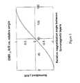
- FIG. 3is a graph illustrating the resistance response of a GMR/TMR multi-layer stack to changes in relative angle between the alternating ferromagnetic layers.
- FIG. 4is a schematic of the cross-section of a TMR sensor stack according to a preferred embodiment of the present invention.
- FIGS. 5 A- 5 Bshow the magnetization configuration of the free and pinned layer net moments before and after the application of external uniaxial stress along the length direction.
- the magnetizationsare shown parallel to each other, providing low resistance to current, and in 5 B, the magnetizations are shown at 90 degrees to each other, providing a higher resistance to current flow.
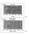
- FIG. 6shows the computation of TMR % as a function of H k,eff according to the present invention.
- FIG. 7shows the computation of TMR % as a function of applied stress in dynes/cm 2 according to the present invention.
- FIG. 8shows the resulting Gauge Factor as a function of applied stress in dynes/cm 2 according to the present invention.
- FIG. 9shows the ability to tailor sensitivity of the device by means of stiffness change in the underlying beam substrate according to the present invention.
- FIG. 10illustrates a beam or diaphragm substrate on which a TMR sensor is deposited and patterned in accordance with the invention.
- FIG. 11illustrates a two dimensional array of beams or diaphragms employing TMR devices such as those illustrated in FIG. 4 and FIG. 5 for use as pressure sensors in accordance with the invention.
- FIG. 12illustrates the use of a conductive layer separated by an insulating spacer from the sensor on the beam, according to the present invention.
- FIG. 13illustrates an example of circuitry for performing electronic measurement in a two dimensional array of pressure sensors employing TMR sensor such as that illustrated in FIG. 10 in accordance with the invention.
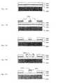
- FIGS. 14 A-Eillustrate a method for fabricating a beam or diaphragm which would employ a TMR device such as that illustrated in FIG. 4 and FIG. 5 for the purpose of pressure sensing in accordance with the invention.
- TMRMagnetic resonance
- the I 2 R heating effectis relatively high for a spin valve sensor that uses the GMR effect, since it uses more current (in the mA range).
- the GMR sensorwill dissipate 1.6 mW
- the TMR sensorwill dissipate 3 orders of magnitude less power.
- the I 2 R heating effectis an important limitation in applications that need a dense array of sensors, such as in fingerprint sensors, and also in situations where temperature control is critical for accurate calibration and reading of strain.
- the temperature of the sensor during operationis a compound effect of both ambient temperature variation and temperature rise due to this intrinsic heat dissipation. Separating these effects involve additional features that add cost, which are eliminated with TMR sensors.
- the absolute value of the magnetoresistive effectis limited for the GMR spin valve sensor to about 15%.
- the magnetoresistive effectcan be as high as 40%. Gage factors can thus be much higher for TMR sensors, as described further hereinafter.
- FIG. 2shows the basic structure of a TMR device, in which there are alternating ferromagnetic layers 12 , made from elements such as Cobalt, Iron or Nickel, are separated by a nonmagnetic insulator layer 14 , such as aluminum oxide to form a sensor 10 .
- a sensor 10such as aluminum oxide
- the electrical resistance of the multi-layer stack of filmsvaries as the relative angle between the magnetizations of the individual ferromagnetic layers, as shown in FIG. 3.
- the resistanceis a minimum when the magnetization vectors between the neighboring ferromagnetic layers are parallel to each other, and is maximum when the two vectors are antiparallel to each other (at 180°), as shown in FIG. 2 and FIG. 3.
- the change in electrical resistance of a TMR multi-layer stack for full rotation of the magnetization vector from a parallel to an antiparallel statecan be anywhere from 2% to 40%, which are approximately twice that of GMR values. Accordingly, one aspect of the present invention is based upon rotating the magnetization of some layers in a TMR multi-layer stack under the application of stress in order to provide a greater sensitivity pressure sensor.
- the rotation of the magnetization vector of a soft ferromagnetic layer that comes about from the magnetoelastic driving forceis proportional to the product of the stress and the magnetostriction.
- the sensors of the present inventionbased upon this concept are multi-layer thin film stacks, which are deposited onto the substrate to be monitored, and photolithographically patterned to a certain aspect ratio, defined as the length/width ratio.
- the free layer's initial magnetic orientation prior to stress applicationis orthogonal to the stress direction, and preferably parallel to the magnetic orientation of the second ferromagnetic pinned layer or SyPL layer.
- a requirement for this magnetization rotationis the sensor's property of magnetostriction, which must be non-zero (>+10 ⁇ 7 or ⁇ 10 ⁇ 7 ), preferably +/ ⁇ 10 ⁇ 5 and whose sign must be appropriate for the sign of the stress.
- the rotation of the magnetizationin turn produces a change in the resistivity of the magnetic material, and, in the presence of voltage applied to the device, causes a corresponding change in the current flow.
- This inventiondescribes a preferred embodiment that uses an antiferromagnetic layer to fix the magnetizations of the pinned ferromagnetic layer.
- the preferred embodimentincludes, in order from the substrate 400 , the underlayer 410 , the (synthetic) free layer 420 , the insulating barrier layer 430 , the (synthetic) pinned layer 440 , the antiferromagnetic pinning layer 450 , and the capping protective layer 460 .
- Each ferromagnetic layer 420 and 440can be a single or multiple layers, and each of the ferromagnetic layers 420 and 440 yield non-zero magnetostriction.
- FIG. 4illustrates an exemplary five layer synthetic ferromagnet structure composed of NiFe 420 - 1 , CoFe 420 - 2 , Ru 420 - 3 , CoFe 420 - 4 and NiFe 420 - 5 .
- the materials used in the compositecan change in type, order, number and other variables to make up the synthetic free layer 420
- NiFe 440 - 1 , CoFe 440 - 2 , Ru 440 - 3 , CoFe 440 - 4 and NiFe 440 - 5make up the preferred synthetic pinned layer 440 , again with the variations of the type noted above being contemplated.
- NiFeCo, Co or other ferromagnetic materialscan also be used for the ferromagnetic layers.
- the thickness of each ferromagnetic layeris typically within the range of 0.1-50 nm.
- the antiferrogmagnetic pinning layercan be made of for example, CrMnPd.
- the capping layercan be made of, for example, Tantalum.
- the barrier layer 430provides for a small ferromagnetic coupling H ilc between the pinned ferromagnetic layer 440 and the free ferromagnetic layer 420 , which in the case of the preferred embodiment is such that the magnetization vectors of the individual layers on either side of the barrier layer 430 are pointed in the same direction and orthogonal to the length of the sensor, as shown in FIG. 5A.
- Barrier layer 430is made of a non-magnetic, electrically insulating material, such as Aluminum Oxide. In the preferred embodiment, the thickness of the barrier layer 430 is within the range of 0.1 to 10 nm.
- the resistance of the sensoris preferably at the extreme value of minimum resistance (parallel net magnetization vectors for free and pinned layers, FIG. 5A) as shown in FIG. 3, left hand side of the graph.
- the resistance of the sensoris determined specifically by the relative angle between the magnetization vectors of the individual ferromagnetic layers 420 and 440 on either side of the barrier layer 430 . Parallelism is described by a zero angle, antiparallelism by 180 degrees, etc.
- the free layer 420Under application of stress, for an appropriate combination of sign of magnetostriction and sign of stress along the length of the sensor, the free layer 420 will rotate towards the length direction, as shown by FIG. 5B. As it rotates, the angle between the moment (or magnetization) vectors of the free layer 420 and pinned layer 440 increases from zero, and the resistance of the device increases. One can thus use this resistance change as a measure of the stress. In the fully saturated state, the moments of the layers 420 and 440 are 90 degrees to each other, and the resistance of the sensor is at the midpoint.
- H ilcthe interlayer coupling field, which can be controlled to approximately 2-5 Oe, in the +y (width) direction, ferromagnetic in nature due to interfacial roughness.
- H k,iintrinsic growth anisotropy, in the +/ ⁇ y direction, induced at film growth.
- H d,fDemagnetization field in the free layer due to charges accumulating at edges. This follows the magnetization and is kept to a minimum (designed out) by utilizing a synthetic free layer with low or no net moment.
- H d,pDemagnetization field in the pinned layer due to charges accumulating at edges. This follows the magnetization and is kept to a minimum (designed out) by utilizing a synthetic pinned layer with low or no net moment.
- H k, ⁇Stress-induced anisotropy in the +/ ⁇ x direction, due to the application of stress.
- H k,effEffective H k in the applied stress (x) direction whose magnitude is equal to H k, ⁇ -H k,i . i.e.
- the output of the sensoris proportional to the average value of a cosine function ⁇ cos>, which is defined as:
- ⁇ cos( ⁇ p ⁇ f )>provides the average value of the cosine of the angle between the magnetizations of the pinned and free layers across the sensor. This varies with applied stress via the property of magnetostriction.
- the average cosine functioncan be determined as a function of H k,eff by deriving and solving the equations for the minimization of magnetic free energy.
- the useful TMR % as a function of H k,effcan then be obtained using the following basic relationship of TMR % to the cosine function:
- TMR %TMR % max ⁇ ( ⁇ cos> f ⁇ cos> i ) 3
- ⁇ COS> fis a function of stress, or more precisely, of the effective anisotropy, H k,eff ., which is the difference between the stress-induced anisotropy and intrinsic anisotropy.
- the TMR % as a function of H k,effis shown graphically in FIG. 6. Note the rapid increase of TMR % with small stress and the asymptotic saturation at higher values. This is a desirable property, since it provides a high sensitivity to the detection of stress, and a “digital” response.
- TMR % maxhas been assumed as 25% and the maximum percent resistance change obtainable is 0.5 TMR % max , due to the 90 degree maximum rotation of the free layer.
- ⁇ and ⁇are magnetostriction and stress, and M s is the saturation magnetization of the free layer.
- the TMR %can be plotted as a function of stress using equation 1 and 4, to generate FIG. 7.
- Gage factorwhich provides a quantitative measure of this sensitivity, is defined as: dR/ ⁇ . It can also be written as dR.E/ ⁇ , where ⁇ is the strain, E the modulus of elasticity, and dR the change in resistance as a percentage. i.e.
- FIG. 8shows the gage factor as a function of stress.
- the maximum gage factoroccurs at very low stress values, which again confirms the high sensitivity of this sensor.
- Conventional sensors for pressure detectionprovide a maximum gage factor in the 75 to 150 range, far below the value of 900 for this TMR sensor.
- the sensorcan be grown on a beam or membrane, whose mechanical properties determine the magnitude of the strain and thus the stress applied to the sensor.
- FIG. 9shows how the gage factor curve can be tailored by the mechanical property of the beams, in this instance two cantilevers with different stiffness constants. Two cantilever substrates are used with different stiffness constants, causing the Gauge Factor curve of each to shift with respect to the applied stress. The stiffness of the cantilevers can be varied by changing their length, width and thickness.
- a multi-layer stack 1010is the basis for a novel stress or pressure sensor, which can be used, for example, for fingerprint sensing.
- the underlying base structure for the TMR sensor 1010is fabricated as a suspended bridge, a cantilevered beam 1004 or a similar kind of membrane that is supported over a cavity 1008 that is formed in a bulk substrate and allows for deformation of the cantilevered beam 1004 , as shown in FIG. 10. An example of a method of fabricating this is described in more detail below.
- a TMR stack 1010comprising the two ferromagnetic layers, the non-magnetic insulating spacer layer and the underlayer and capping layers are deposited on deformable beam 1004 , and leads 1012 are connected thereto to apply a voltage across it and to measure the resulting spin-polarized tunneling current and resistance.
- the support structure for TMR layer 1010can be a variety of different structures other than the beam 1004 of this example, such as a sealed membrane over an enclosure, or any other form that may be suitable for detecting deflection and stress. An example would be where the TMR sensor is located under the beam, and thus subjected to compressive rather than tensile stresses.
- the stress directionneeds to be either unidirectional or if bidirectional, needs to be different along the two principal axes. If the length of the beam is “L”, the width “W”, and the thickness “t”, for a load “4Q” acting on a length L/4 at the end, the maximum tensile stress at the base of the beam where the sensor is located is approximately given by:
- Mis the bending moment
- Iis the moment of inertia about the vertical axis.
- the maximum stress and strainoccur on the surface of the beam. Since the multi-layer stack 1010 is located on the surface of the beam 1004 , and is a very thin set of films, for calculation and illustration purposes, one can assume that the TMR element is subjected to the maximum stress and strain.
- the multi-layer stackis subjected to the maximum tensile stress on the beam surface, as the beam bends in response to applied pressure.
- the magnetostriction of the devicecauses the resistance of the element to change depending on the sign of the applied stress, as described earlier. In this way, by measuring the resistance prior to and during the application of the stress, the difference in resistance gives a good indication of the magnitude of the stress. If the system is calibrated, this can give an idea of the absolute stress as well as just the presence of a pressure point.
- the sensitivity of the device as described aboveexceeds the sensitivity of a capacitance-based sensor or a piezoresistive sensor.
- TMR sensor 1010the TMR element can be made as small as 4 microns long and 3 microns wide while maintaining considerable sensitivity. It is desirable to make the beam as long as possible within the constraints of the product, because sensitivity only improves with the length of the beam.
- a tunneling magnetoresistive pressure sensor 1102(that can be used for fingerprint verification/identification, for example) employing TMR sensors 1110 as described above will now be described in detail with reference to FIG. 11.
- TMR sensors 1110as described above are placed in an array 1106 of m rows by n columns on a substrate 1104 , with a very fine pitch, and connected to electrodes 1108 . Because the sensors can be made as small as 4 microns in length, the lateral resolution can easily satisfy requirements which are typically set for fingerprint applications, such as 500 dots per inch, as well as even more stringent requirements.
- the ridges on the fingers(which are spaced at about 400-500 microns, and are therefore considerably wider than the sensor pitch in the array), apply a force on the sensors that they come in contact with.
- the sensors that fall between the ridgesexperience little to no stress. In this way, one can generate a map of the contact points or the ridges on the fingerprint, and get an accurate reproduction of the fingerprint.
- the sensor length and pitchcan be made greater than 5 microns, since such a good resolution is typically not required for a fingerprint image.
- the processing time for the imageincreases, since the number of sensors in the image increases as well.
- the length of the multi-layer stackis typically in the range of 2-200 microns, and the width is in the range of 0.1-100 microns.
- the sensor dimensionsare preferably 0.5-5 micron wide and 5-10 micron long.
- FIG. 12shows a fixed beam 1204 disposed over a cavity 1202 , with TMR stack 1210 formed in this example on the center of the beam 1204 .
- a layer of insulating material 1212then coated on top of the GMR stack 1210 , and then another layer 1214 of a conductive metal (such as Titanium, copper, etc.) is deposited, whose purpose is to bleed off transient charges caused by ESD and protect the sensor from ESD damage.
- This conductive film 1214needs to be grounded, so that the charges from the transient voltage spikes can be bled to ground. This is illustrated in FIG.
- grounding leads 1216 A and 1216 Bshown from the conductive layer in order to dissipate ESD charges to ground that is within the substrate.
- Another embodiment for ESD protectionputs the sensor on the underside of the deflecting beam or membrane, such that the beam material and thickness act as a protective shield against ESD.
- a hard coatingcan be deposited both above and below the conductive ESD protection layer.
- the thicknesses of all these layerswould be in the range of 0.001 ⁇ m-10 ⁇ m.
- the material used for the mechanically protective coatingscould be a material such as carbon based material, such as “diamond like carbon” or silicon carbide, for example. These materials can also be tailored to have surface energies such that undesired deposits, such as debris or oils from the finger, are prevented from adhering to the coating.
- FIG. 13An example of electronic circuitry and a method that can be used to probe an array of sensors either individually or as a group is shown in FIG. 13. It includes a decoder 1302 , a multiplexer 1304 , and amplifier 1306 , and A/D converter 1308 .
- the techniques for providing such electronic circuitry and method according to this exampleare well known and detailed descriptions thereof are not necessary for an understanding of the present invention. It is noted that there are several different methods of scanning and addressing the array. One approach is shown in FIG. 13, which employs transistors or diodes to isolate each element of the array during addressing of the array. An alternate cell addressing method is described in U.S. patent application Ser. No. 09/571,765, filed May 16, 2000 entitled “Method and Apparatus for Pressure Sensing”, and does not require the use of transistors or diodes to address each element of the array.
- a baselineis first established that determines whether there is a stress on a particular sensor with no finger on the sensor, wherein the “quiescent” resistance of each element of the array is measured. Then the readings are repeated with the finger on the sensor, and the difference in voltages/currents between the “quiescent, unstressed” state and the “stressed” state is calculated to determine the fingerprint pattern.
- the baselinecan desirably be established either immediately prior to or immediately following the imaging of the fingerprint. While one method of scanning, providing power to each element, selectively addressing each element either using transistors or diodes, as shown in FIG. 13, or the cell addressing method described in U.S.
- An advantage of the method of establishing a baseline in this inventionis that it always establishes a reference value, which eliminates the effect of ambient temperature, humidity, stress, etc.
- the prior artusing capacitive or optical means are unable to obtain such a reference each time a measurement is taken, because they depend on the presence of a finger to obtain a reading each time. Even though the resistance of the sensor changes with temperature, this effect can be automatically compensated for by establishing a reference value, either immediately prior to or immediately following the fingerprint imaging, as noted above.
- FIG. 14AAn example of a method for manufacturing a magnetoresistive sensor in accordance with the invention will now be described with reference to FIG. 14.
- a layer of silicon nitride 1404is first deposited on a silicon substrate 1402 , then a layer of polysilicon 1406 , followed by another layer of silicon nitride 1408 .
- the pattern of the beamis etched using photolithography by depositing a layer of photoresist 1410 as shown in FIG. 14B, and etching through at least the top two layers of silicon nitride and polysilicon as shown in FIG. 14C.
- Thisis followed by preferentially etching out the second layer of polysilicon underneath the silicon nitride in the beam portion 1412 , thus forming a simply suspended beam 1412 of the upper layer of silicon nitride as shown in FIG. 14D.
- a thin silicon beam or membraneis made by starting from a silicon wafer using conventional processing means as have been described elsewhere in the literature. This is typically done either by etching from the back side using anisotropic etchants, or using single sided wafer processing, by first doping the wafer with n-type doping elements (arsenic), covering with a layer of epitaxial silicon, then etching using a chlorine gas plasma to preferentially etch the N+ region. The preferential etching of the N+ region under the top layer of epitaxial silicon leaves the upper layer suspended as a beam, supported on either side.
- n-type doping elementsarsenic
- a series of thin filmsis deposited using thin film techniques (typically a cluster tool), representing the magnetoresistive “stack”.
- This series of materialscomprises a tantalum layer (the underlayer), the free layer (or synthetic free layer stack SyFL), the barrier layer of aluminum oxide, the pinned layer (or synthetic pinned layer stack SyPL), the antiferromagnet layer, and finally the capping layer.
- This stack of thin filmsis deposited on the entire substrate, and therefore will cover the beam, and the exposed portions of the recess under the beam.
- the beamcan be made anywhere from 0.2 micron to 20 microns thick; the length of the beam can range from 2 micron to several hundred microns, and the width of the beam can range from 2 micron to several microns. These parameters depend on the mechanical properties of the substrate material used to create the beam, and on the sensitivity required.
- the beamcan be designed to either have “standoff” from the substrate, or can be a free standing structure, with the bottom of the substrate completely etched out.
Landscapes
- Engineering & Computer Science (AREA)
- Physics & Mathematics (AREA)
- General Physics & Mathematics (AREA)
- Human Computer Interaction (AREA)
- Multimedia (AREA)
- Theoretical Computer Science (AREA)
- Hall/Mr Elements (AREA)
- Measuring Fluid Pressure (AREA)
Abstract
Description
- The present invention relates to Tunneling MagnetoResistive (TMR) devices in conjunction with micromachined beams to measure stresses with high sensitivity, and methods of making and using the same.[0001]
- Historically, fingerprint image-capture devices have used optical-based sensors or capacitance-based sensors. With reference to the specific example of a fingerprint, optical sensors use a light source, lenses and a prism to image the “ridges” and valleys on the fingerprint, based on differences in the reflected light from the features. The conventional capacitance sensor uses semiconductor type processing to fabricate a two-dimensional array of capacitors. The individual sensors form one plate of the parallel plate capacitor, while the finger itself, when placed on the array, acts as the second plate. Upon contact with the array of sensors, the individual distance from each sensor to the skin is measured using capacitive techniques. The difference in distance to skin at the ridges and valleys of a fingerprint provide the means to replicate the fingerprint. An example of the use of capacitive sensors to measure the spacing is shown in FIGS. 1A and 1B.[0002]
- Both the above techniques fundamentally measure the spacing between the fingerprint features, and the sensor. The measurement of spacing is inherently subject to several distortion effects: since the height difference between the ridges and valleys is only of the order of 50 microns, any parameter which affects the spacing between the finger and the sensor will affect the measurement. For example, both types of sensors are very sensitive to the thickness of the protective coating. They are also sensitive to oils or grease on the finger, and the presence or absence of moisture on the finger. In addition, most of these sensors are adversely affected by ambient temperature at the time of sensing, as well as electrostatic discharge (ESD). Under very hot or very cold conditions, the capacitive sensor can provide erroneous readings. ESD can altogether destroy a sensor. The combined effect of all these variables results in a very distorted image, if any, of the fingerprint, as shown in FIG. 1C.[0003]
- As a result of the above drawbacks to spacing based reproduction of fingerprints, it would be very useful to be able to use the difference in pressure exerted by the ridges and valleys of a fingerprint on a sensor to replicate the fingerprint image. In principle, a pressure-based fingerprint sensor would be impervious to the drawbacks listed above, such as wet or dry conditions on the fingertip, presence of oil or grease on the fingertip, thickness of protective coatings, etc., providing a “digital” response, depending on whether the sensor experiences a ridge or not. This situation is illustrated in FIGS. 1D and 1E, where the pressure sensor can highlight only the ridges, which are the lines of interest in a fingerprint. However, due to a variety of factors, including the very low sensitivity and inability to provide the required resolution, pressure based sensors have not been deployed for the replication of fingerprints.[0004]
- Improvements in pressure sensors are described in U.S. patent application Ser. No. 09/500,706 entitled “Magnetoresistive Semiconductor Pressure Sensor and Fingerprint/Verification Sensors Using the Same” and U.S. patent application Ser. No. 09/502,406 entitled “Use of Multi-Layer Thin Films as Stress Sensors, Appln., both assigned to the same assignee as the present invention. These applications describe many different improved aspects of pressure sensors, including sensors based upon magnetostriction and the GMR effect.[0005]
- While the above applications provide many advantages, improvements that can result in greater sensitivity, less power consumption and lower thermal build-up are nonetheless desirable.[0006]
- The present invention, as described below, described such a device, which, as one of it aspects, operates using the Tunneling MagnetoResistive (TMR) effect. The TMR effect was discovered relatively recently in the mid 1980's by Julliere et al. Since then researchers in the area of random access and flash semiconductor memories have explored the TMR principle to enhance the utility of such devices. This research, however, has been limited to these areas, and has not been reported as having usefulness in the context of fingerprint and pressure sensing applications.[0007]
- It is an object of the present invention to provide a TMR sensor for the detection of pressure or stress.[0008]
- It is an object of the present invention to provide a TMR sensor that includes two ferromagnetic layers separated by an electron-tunneling barrier, with electrical Current flowing Perpendicular to the Plane of the layers (CPP).[0009]
- It is another object of the current invention to magnetically pin one ferromagnetic layer while allowing the other ferromagnetic layer to rotate freely under the action of an externally applied stress.[0010]
- It is another object of the current invention to reduce the magnetic moment of the free ferromagnetic layer by forming a composite trilayer stack containing a ferromagnetic layer, a spacer layer, and another antiferromagnetically-coupled ferromagnetic layer, referred to together as the synthetic free layer (SyFL).[0011]
- It is another object of the current invention to reduce the magnetic moment of the pinned ferromagnetic layer by forming a composite trilayer stack containing a ferromagnetic layer, a spacer layer, and another antiferromagnetically-coupled ferromagnetic layer, referred to together as the synthetic pinned layer (SyPL).[0012]
- It is a further object of the present invention to provide a TMR sensor capable of sensing both compressive stress and tension.[0013]
- It a further object of the present invention is to provide a TMR sensor that is protected from Electro-Static Discharge (ESD).[0014]
- It is a further object of the present invention to provide a TMR sensor that can be adapted to have substantial independence from temperature shifts.[0015]
- Another object of the invention is to provide a TMR sensor that is suitable for use in fingerprint identification and verification.[0016]
- Another object of the invention is to provide a TMR sensor that is suitable for use in fingerprint identification and verification and that is less sensitive to adverse conditions such as extreme temperatures and skin oils and grease.[0017]
- The present invention fulfills these and other objects of the present invention, by providing a pressure sensing device that includes at least one lithographically patterned TMR sensor, but preferably an array of TMR sensors, with each TMR sensor having an insulating spacer layer interposed between a free and a pinned ferromagnetic layer. In an unbiased state, the magnetization vectors of the ferromagnetic layers are preferably parallel to each other, but can also be antiparallel to each other and still remain stable with respect to each other. Upon application of a small voltage, the magnetization vectors remain unchanged. Upon application of stress, the magnetization vector of the free layer will rotate away from parallelism with the pinned layer, thus causing a corresponding and proportionally related change in the resistance of the magnetic material of the sensor. This change in resistance can be sensed and used to calculate the stress applied thereto.[0018]
- While the above provides an overview of the invention, there exist numerous other significant aspects and advantages that will become apparent in the discussion provided hereinafter. In this regard, for instance, reference to a free layer magnetization can interchangeably reference the net moment of a synthetic free layer stack. The same holds for the pinned layer, which can just as well be replaced with a synthetic pinned layer stack.[0019]
- The above and other objectives, features, and advantages of the present invention are further described in the detailed description which follows, with reference to the drawings by way of non-limiting exemplary embodiments of the present invention, wherein like reference numerals represent similar parts of the present invention throughout several views and wherein:[0020]
- FIGS.[0021]1A-1E are side views of a fingertip on a prior art capacitive sensor, and on a potential pressure sensor according to the present invention which illustrate the use of spacing versus pressure for replicating the fingerprint, and the distortion associated with the prior art.
- FIG. 2 is a schematic view of a conventional TMR multi-layer stack, using alternating ferromagnetic layers separated by a non-magnetic insulating spacer.[0022]
- FIG. 3 is a graph illustrating the resistance response of a GMR/TMR multi-layer stack to changes in relative angle between the alternating ferromagnetic layers.[0023]
- FIG. 4 is a schematic of the cross-section of a TMR sensor stack according to a preferred embodiment of the present invention.[0024]
- FIGS.[0025]5A-5B show the magnetization configuration of the free and pinned layer net moments before and after the application of external uniaxial stress along the length direction. In5A, the magnetizations are shown parallel to each other, providing low resistance to current, and in5B, the magnetizations are shown at 90 degrees to each other, providing a higher resistance to current flow.
- FIG. 6 shows the computation of TMR % as a function of H[0026]k,effaccording to the present invention.
- FIG. 7 shows the computation of TMR % as a function of applied stress in dynes/cm[0027]2according to the present invention.
- FIG. 8 shows the resulting Gauge Factor as a function of applied stress in dynes/cm[0028]2according to the present invention.
- FIG. 9 shows the ability to tailor sensitivity of the device by means of stiffness change in the underlying beam substrate according to the present invention.[0029]
- FIG. 10 illustrates a beam or diaphragm substrate on which a TMR sensor is deposited and patterned in accordance with the invention.[0030]
- FIG. 11 illustrates a two dimensional array of beams or diaphragms employing TMR devices such as those illustrated in FIG. 4 and FIG. 5 for use as pressure sensors in accordance with the invention.[0031]
- FIG. 12 illustrates the use of a conductive layer separated by an insulating spacer from the sensor on the beam, according to the present invention.[0032]
- FIG. 13 illustrates an example of circuitry for performing electronic measurement in a two dimensional array of pressure sensors employing TMR sensor such as that illustrated in FIG. 10 in accordance with the invention.[0033]
- FIGS.[0034]14A-E illustrate a method for fabricating a beam or diaphragm which would employ a TMR device such as that illustrated in FIG. 4 and FIG. 5 for the purpose of pressure sensing in accordance with the invention.
- The working principle of TMR has certain similarities to that of GMR, since in both TMR sensors (as described herein) and GMR sensors, a change in applied pressure will cause a rotation of the magnetization associated with the device, and a corresponding change in resistance, which can be sensed. Further, in both devices, there is a stack of layers, in which the innermost and outermost layers are made of ferromagnetic materials. Despite those similarities, implementation of a TMR device is very different from implementation of a GMR device. In particular, this is due to the fact that the layer between the inner and outer ferromagnetic layers is an insulating, rather than a conducting material, and the electrical current flows perpendicular to the plane of the layers, rather than in the plane of the layers.[0035]
- As a result of these differences, the following observations have been noted by the present inventors, which lead to the conclusion that a TMR device can have advantages to GMR device when both are used as a sensitive strain gauge.[0036]
- Firstly, due to the low resistance of a GMR device, electrical currents in the milliampere range are required for generating sufficient output voltage. For example, for a typical GMR sensor with 100 ohm resistance and 5% usable GMR effect, a 2 mA current will produce a voltage output of only 10 mV, but a 4 mA current will produce a more measurable output of 20 mV. This quadruples the power requirement of the device. By comparison, a TMR device with a resistance of 105 ohms and 10% usable TMR effect will produce the same output voltage of 20 mV with only 2 μA current flowing.[0037]
- Secondly, the I[0038]2R heating effect is relatively high for a spin valve sensor that uses the GMR effect, since it uses more current (in the mA range). In the example cited in the paragraph above, the GMR sensor will dissipate 1.6 mW, whereas the TMR sensor will dissipate 3 orders of magnitude less power. Thus, the I2R heating effect is an important limitation in applications that need a dense array of sensors, such as in fingerprint sensors, and also in situations where temperature control is critical for accurate calibration and reading of strain. With the GMR sensor, the temperature of the sensor during operation is a compound effect of both ambient temperature variation and temperature rise due to this intrinsic heat dissipation. Separating these effects involve additional features that add cost, which are eliminated with TMR sensors.
- Thirdly, and specifically in situations such as fingerprint sensors where large sensor arrays are used, the mA current per sensor requirement causes another undesirable side effect. This is the exceedingly high total current flowing through all the sensors in the array. For a 256×256 array, this could quite easily exceed 1 Ampere. The external circuits have to be made robust to deal with such high currents, which will again increase the total cost to the user, or make the product cost-ineffective.[0039]
- Fourthly, the absolute value of the magnetoresistive effect is limited for the GMR spin valve sensor to about 15%. For a tunneling spin valve sensor, by comparison, the magnetoresistive effect can be as high as 40%. Gage factors can thus be much higher for TMR sensors, as described further hereinafter.[0040]
- FIG. 2 shows the basic structure of a TMR device, in which there are alternating[0041]
ferromagnetic layers 12, made from elements such as Cobalt, Iron or Nickel, are separated by anonmagnetic insulator layer 14, such as aluminum oxide to form asensor 10. When an electrical current is imposed across the thickness direction of the sensor (Current Perpendicular to Plane or CPP direction), the electrical resistance of the multi-layer stack of films varies as the relative angle between the magnetizations of the individual ferromagnetic layers, as shown in FIG. 3. The resistance is a minimum when the magnetization vectors between the neighboring ferromagnetic layers are parallel to each other, and is maximum when the two vectors are antiparallel to each other (at 180°), as shown in FIG. 2 and FIG. 3. - The change in electrical resistance of a TMR multi-layer stack for full rotation of the magnetization vector from a parallel to an antiparallel state can be anywhere from 2% to 40%, which are approximately twice that of GMR values. Accordingly, one aspect of the present invention is based upon rotating the magnetization of some layers in a TMR multi-layer stack under the application of stress in order to provide a greater sensitivity pressure sensor.[0042]
- Before describing the initial preferred embodiment in detail, an overview of the concepts that are used by the present invention will be first provided. Subsequently, the preferred embodiments and alternative embodiments will be discussed.[0043]
- The rotation of the magnetization vector of a soft ferromagnetic layer that comes about from the magnetoelastic driving force is proportional to the product of the stress and the magnetostriction. The sensors of the present invention based upon this concept are multi-layer thin film stacks, which are deposited onto the substrate to be monitored, and photolithographically patterned to a certain aspect ratio, defined as the length/width ratio. A uniaxial compressive or tensile stress in bending, acting upon the flexible beam substrate and therefore upon the sensor, preferably along its length, produces a rotation of the magnetization vector of the free layer or SyFL layer, even under the absence of an external magnetic field. The free layer's initial magnetic orientation prior to stress application is orthogonal to the stress direction, and preferably parallel to the magnetic orientation of the second ferromagnetic pinned layer or SyPL layer. A requirement for this magnetization rotation is the sensor's property of magnetostriction, which must be non-zero (>+10[0044]−7or <−10−7), preferably +/−10−5and whose sign must be appropriate for the sign of the stress. The rotation of the magnetization in turn produces a change in the resistivity of the magnetic material, and, in the presence of voltage applied to the device, causes a corresponding change in the current flow.
- This invention describes a preferred embodiment that uses an antiferromagnetic layer to fix the magnetizations of the pinned ferromagnetic layer. Specifically, as shown in FIG. 4, the preferred embodiment includes, in order from the[0045]
substrate 400, the underlayer410, the (synthetic)free layer 420, the insulatingbarrier layer 430, the (synthetic) pinnedlayer 440, the antiferromagnetic pinninglayer 450, and the cappingprotective layer 460. Eachferromagnetic layer ferromagnetic layers - FIG. 4 illustrates an exemplary five layer synthetic ferromagnet structure composed of NiFe[0046]420-1, CoFe420-2, Ru420-3, CoFe420-4 and NiFe420-5. Of course, the materials used in the composite can change in type, order, number and other variables to make up the synthetic
free layer 420, and NiFe440-1, CoFe440-2, Ru440-3, CoFe440-4 and NiFe440-5 make up the preferred synthetic pinnedlayer 440, again with the variations of the type noted above being contemplated. NiFeCo, Co or other ferromagnetic materials can also be used for the ferromagnetic layers. The thickness of each ferromagnetic layer is typically within the range of 0.1-50 nm. The antiferrogmagnetic pinning layer can be made of for example, CrMnPd. The capping layer can be made of, for example, Tantalum. - The[0047]
barrier layer 430 provides for a small ferromagnetic coupling Hilcbetween the pinnedferromagnetic layer 440 and the freeferromagnetic layer 420, which in the case of the preferred embodiment is such that the magnetization vectors of the individual layers on either side of thebarrier layer 430 are pointed in the same direction and orthogonal to the length of the sensor, as shown in FIG. 5A.Barrier layer 430 is made of a non-magnetic, electrically insulating material, such as Aluminum Oxide. In the preferred embodiment, the thickness of thebarrier layer 430 is within the range of 0.1 to 10 nm. - In the quiescent, zero stress state of the device, the resistance of the sensor is preferably at the extreme value of minimum resistance (parallel net magnetization vectors for free and pinned layers, FIG. 5A) as shown in FIG. 3, left hand side of the graph. The resistance of the sensor is determined specifically by the relative angle between the magnetization vectors of the individual[0048]
ferromagnetic layers barrier layer 430. Parallelism is described by a zero angle, antiparallelism by 180 degrees, etc. - Under application of stress, for an appropriate combination of sign of magnetostriction and sign of stress along the length of the sensor, the[0049]
free layer 420 will rotate towards the length direction, as shown by FIG. 5B. As it rotates, the angle between the moment (or magnetization) vectors of thefree layer 420 and pinnedlayer 440 increases from zero, and the resistance of the device increases. One can thus use this resistance change as a measure of the stress. In the fully saturated state, the moments of thelayers - That a useful resistance change can be achieved as a result of the magnetization of the sensor films can be shown with reference to an exemplary sensor having an aspect ratio of 1.5. Where:[0050]
- H[0051]ilc: the interlayer coupling field, which can be controlled to approximately 2-5 Oe, in the +y (width) direction, ferromagnetic in nature due to interfacial roughness.
- H[0052]k,i: intrinsic growth anisotropy, in the +/−y direction, induced at film growth.
- H[0053]d,f: Demagnetization field in the free layer due to charges accumulating at edges. This follows the magnetization and is kept to a minimum (designed out) by utilizing a synthetic free layer with low or no net moment.
- H[0054]d,p: Demagnetization field in the pinned layer due to charges accumulating at edges. This follows the magnetization and is kept to a minimum (designed out) by utilizing a synthetic pinned layer with low or no net moment.
- H[0055]k,σ: Stress-induced anisotropy in the +/−x direction, due to the application of stress.
- H[0056]k,eff: Effective Hkin the applied stress (x) direction whose magnitude is equal to Hk,σ-Hk,i. i.e.
- Hk,eff=Hk,σ−Hk,i 1
- The output of the sensor is proportional to the average value of a cosine function <cos>, which is defined as:[0057]
- <cos>=(1−<cos(θp−θf)>)/2 2
- <cos(θ[0058]p−θf)> provides the average value of the cosine of the angle between the magnetizations of the pinned and free layers across the sensor. This varies with applied stress via the property of magnetostriction. The average cosine function can be determined as a function of Hk,effby deriving and solving the equations for the minimization of magnetic free energy. The useful TMR % as a function of Hk,effcan then be obtained using the following basic relationship of TMR % to the cosine function:
- TMR %=TMR %max×(<cos>f−<cos>i) 3
- The subscripts f and i are for final and initial states, i.e. stressed and unstressed states.[0059]
- In equation 3, <COS>[0060]fis a function of stress, or more precisely, of the effective anisotropy, Hk,eff., which is the difference between the stress-induced anisotropy and intrinsic anisotropy. The TMR % as a function of Hk,effis shown graphically in FIG. 6. Note the rapid increase of TMR % with small stress and the asymptotic saturation at higher values. This is a desirable property, since it provides a high sensitivity to the detection of stress, and a “digital” response. TMR %maxhas been assumed as 25% and the maximum percent resistance change obtainable is 0.5 TMR %max, due to the 90 degree maximum rotation of the free layer.
- The equation that describes the relationship of H[0061]k,σto stress is:
- Hk,σ=3×λ×σ/
M s 4 - Where λ and σ are magnetostriction and stress, and M[0062]sis the saturation magnetization of the free layer.
- The TMR % can be plotted as a function of[0063]
stress using equation 1 and 4, to generate FIG. 7. - The rapid rise of TMR % with low stress values (low 1e8 range, in dyn/cm2) shows the sensitivity of the sensor more clearly.[0064]
- Gage factor, which provides a quantitative measure of this sensitivity, is defined as: dR/ε. It can also be written as dR.E/σ, where ε is the strain, E the modulus of elasticity, and dR the change in resistance as a percentage. i.e.[0065]
- g.f.=dR.E/σ 5
- Substituting the values into equation 5, FIG. 8 can be generated, which shows the gage factor as a function of stress. The maximum gage factor occurs at very low stress values, which again confirms the high sensitivity of this sensor. Conventional sensors for pressure detection provide a maximum gage factor in the 75 to 150 range, far below the value of 900 for this TMR sensor.[0066]
- The sensor can be grown on a beam or membrane, whose mechanical properties determine the magnitude of the strain and thus the stress applied to the sensor. FIG. 9 shows how the gage factor curve can be tailored by the mechanical property of the beams, in this instance two cantilevers with different stiffness constants. Two cantilever substrates are used with different stiffness constants, causing the Gauge Factor curve of each to shift with respect to the applied stress. The stiffness of the cantilevers can be varied by changing their length, width and thickness.[0067]
- Pressure sensor application of the TMR Sensor[0068]
- In accordance with an aspect of the invention, a[0069]
multi-layer stack 1010 is the basis for a novel stress or pressure sensor, which can be used, for example, for fingerprint sensing. In order to use it, the underlying base structure for theTMR sensor 1010 is fabricated as a suspended bridge, acantilevered beam 1004 or a similar kind of membrane that is supported over acavity 1008 that is formed in a bulk substrate and allows for deformation of the cantileveredbeam 1004, as shown in FIG. 10. An example of a method of fabricating this is described in more detail below. ATMR stack 1010 comprising the two ferromagnetic layers, the non-magnetic insulating spacer layer and the underlayer and capping layers are deposited ondeformable beam 1004, and leads1012 are connected thereto to apply a voltage across it and to measure the resulting spin-polarized tunneling current and resistance. It should be apparent that the support structure forTMR layer 1010 can be a variety of different structures other than thebeam 1004 of this example, such as a sealed membrane over an enclosure, or any other form that may be suitable for detecting deflection and stress. An example would be where the TMR sensor is located under the beam, and thus subjected to compressive rather than tensile stresses. - Under the application of a force on the[0070]
beam 1004, it deflects. Note that in this configuration of the beam, the stress direction needs to be either unidirectional or if bidirectional, needs to be different along the two principal axes. If the length of the beam is “L”, the width “W”, and the thickness “t”, for a load “4Q” acting on a length L/4 at the end, the maximum tensile stress at the base of the beam where the sensor is located is approximately given by: - σmax=Mt/2I=(7/16)QL2t/
I 6 - where M is the bending moment, and I is the moment of inertia about the vertical axis.[0071]
- The maximum stress and strain occur on the surface of the beam. Since the[0072]
multi-layer stack 1010 is located on the surface of thebeam 1004, and is a very thin set of films, for calculation and illustration purposes, one can assume that the TMR element is subjected to the maximum stress and strain. - Under these conditions, the multi-layer stack is subjected to the maximum tensile stress on the beam surface, as the beam bends in response to applied pressure. The magnetostriction of the device causes the resistance of the element to change depending on the sign of the applied stress, as described earlier. In this way, by measuring the resistance prior to and during the application of the stress, the difference in resistance gives a good indication of the magnitude of the stress. If the system is calibrated, this can give an idea of the absolute stress as well as just the presence of a pressure point.[0073]
- In accordance with an aspect of the invention, the sensitivity of the device as described above exceeds the sensitivity of a capacitance-based sensor or a piezoresistive sensor. As a result, considerable miniaturization can be realized with[0074]
TMR sensor 1010. With conventional fabrication methods, the TMR element can be made as small as 4 microns long and 3 microns wide while maintaining considerable sensitivity. It is desirable to make the beam as long as possible within the constraints of the product, because sensitivity only improves with the length of the beam. - In order to achieve the maximum sensitivity of the sensor to an applied stress, it is appropriate to choose an alloy and deposition conditions that would ensure a maximum ΔR/R response from the material, as well as a maximum magnetostriction coefficient.[0075]
- A tunneling magnetoresistive pressure sensor[0076]1102 (that can be used for fingerprint verification/identification, for example) employing TMR sensors1110 as described above will now be described in detail with reference to FIG. 11. Several sensors1110 as described above are placed in an
array 1106 of m rows by n columns on asubstrate 1104, with a very fine pitch, and connected toelectrodes 1108. Because the sensors can be made as small as 4 microns in length, the lateral resolution can easily satisfy requirements which are typically set for fingerprint applications, such as 500 dots per inch, as well as even more stringent requirements. For example, when a finger is placed on the array, the ridges on the fingers (which are spaced at about 400-500 microns, and are therefore considerably wider than the sensor pitch in the array), apply a force on the sensors that they come in contact with. The sensors that fall between the ridges experience little to no stress. In this way, one can generate a map of the contact points or the ridges on the fingerprint, and get an accurate reproduction of the fingerprint. However, in practice, the sensor length and pitch can be made greater than 5 microns, since such a good resolution is typically not required for a fingerprint image. Moreover, as the sensor pitch decreases, the processing time for the image increases, since the number of sensors in the image increases as well. The length of the multi-layer stack is typically in the range of 2-200 microns, and the width is in the range of 0.1-100 microns. For a fingerprint image capture application, the sensor dimensions are preferably 0.5-5 micron wide and 5-10 micron long. - In order to protect the TMR sensor during its use as a fingerprint sensor, different schemes may be used. For ESD protection, FIG. 12 shows a fixed beam[0077]1204 disposed over a
cavity 1202, withTMR stack 1210 formed in this example on the center of the beam1204. A layer of insulatingmaterial 1212 then coated on top of theGMR stack 1210, and then anotherlayer 1214 of a conductive metal (such as Titanium, copper, etc.) is deposited, whose purpose is to bleed off transient charges caused by ESD and protect the sensor from ESD damage. Thisconductive film 1214 needs to be grounded, so that the charges from the transient voltage spikes can be bled to ground. This is illustrated in FIG. 12, with grounding leads1216A and1216B shown from the conductive layer in order to dissipate ESD charges to ground that is within the substrate. Another embodiment for ESD protection puts the sensor on the underside of the deflecting beam or membrane, such that the beam material and thickness act as a protective shield against ESD. - Secondly, to protect the TMR stack from mechanical abrasion or small impact, a hard coating can be deposited both above and below the conductive ESD protection layer. The thicknesses of all these layers would be in the range of 0.001 μm-10 μm. The material used for the mechanically protective coatings could be a material such as carbon based material, such as “diamond like carbon” or silicon carbide, for example. These materials can also be tailored to have surface energies such that undesired deposits, such as debris or oils from the finger, are prevented from adhering to the coating.[0078]
- An example of electronic circuitry and a method that can be used to probe an array of sensors either individually or as a group is shown in FIG. 13. It includes a[0079]
decoder 1302, amultiplexer 1304, andamplifier 1306, and A/D converter 1308. The techniques for providing such electronic circuitry and method according to this example are well known and detailed descriptions thereof are not necessary for an understanding of the present invention. It is noted that there are several different methods of scanning and addressing the array. One approach is shown in FIG. 13, which employs transistors or diodes to isolate each element of the array during addressing of the array. An alternate cell addressing method is described in U.S. patent application Ser. No. 09/571,765, filed May 16, 2000 entitled “Method and Apparatus for Pressure Sensing”, and does not require the use of transistors or diodes to address each element of the array. - In accordance with an aspect of a method of fingerprint identification/verification in accordance with the invention, a baseline is first established that determines whether there is a stress on a particular sensor with no finger on the sensor, wherein the “quiescent” resistance of each element of the array is measured. Then the readings are repeated with the finger on the sensor, and the difference in voltages/currents between the “quiescent, unstressed” state and the “stressed” state is calculated to determine the fingerprint pattern. The baseline can desirably be established either immediately prior to or immediately following the imaging of the fingerprint. While one method of scanning, providing power to each element, selectively addressing each element either using transistors or diodes, as shown in FIG. 13, or the cell addressing method described in U.S. patent application Ser. No. 09/571,765, filed May 16, 2000 entitled “Method and Apparatus for Pressure Sensing”, conversion of values from analog to digital, etc are well known.[0080]
- An advantage of the method of establishing a baseline in this invention is that it always establishes a reference value, which eliminates the effect of ambient temperature, humidity, stress, etc. The prior art, using capacitive or optical means are unable to obtain such a reference each time a measurement is taken, because they depend on the presence of a finger to obtain a reading each time. Even though the resistance of the sensor changes with temperature, this effect can be automatically compensated for by establishing a reference value, either immediately prior to or immediately following the fingerprint imaging, as noted above.[0081]
- It should be apparent to those skilled in the art that since the TMR sensor's output depends on a number of factors, it can be used in a variety of alternative ways in this and other embodiments other than for fingerprint identification/verification.[0082]
- An example of a method for manufacturing a magnetoresistive sensor in accordance with the invention will now be described with reference to FIG. 14. As shown in FIG. 14A, a layer of[0083]
silicon nitride 1404 is first deposited on asilicon substrate 1402, then a layer ofpolysilicon 1406, followed by another layer ofsilicon nitride 1408. Then the pattern of the beam is etched using photolithography by depositing a layer ofphotoresist 1410 as shown in FIG. 14B, and etching through at least the top two layers of silicon nitride and polysilicon as shown in FIG. 14C. This is followed by preferentially etching out the second layer of polysilicon underneath the silicon nitride in thebeam portion 1412, thus forming a simply suspendedbeam 1412 of the upper layer of silicon nitride as shown in FIG. 14D. - Alternatively, using similar techniques as are known in the art, a thin silicon beam or membrane is made by starting from a silicon wafer using conventional processing means as have been described elsewhere in the literature. This is typically done either by etching from the back side using anisotropic etchants, or using single sided wafer processing, by first doping the wafer with n-type doping elements (arsenic), covering with a layer of epitaxial silicon, then etching using a chlorine gas plasma to preferentially etch the N+ region. The preferential etching of the N+ region under the top layer of epitaxial silicon leaves the upper layer suspended as a beam, supported on either side.[0084]
- It should be noted that even though the manufacturing descriptions above are for the processing of silicon, one can use other materials to achieve the same purpose as well. For example, one could use a substrate of Aluminum, coat it with a layer of insulating alumina (using thin film deposition techniques that are well known), sputter another layer of metal (such as aluminum, titanium, copper, etc.). One can now perform photolithography and use dry etching techniques (such as ion milling) to etch down to the underlying layer of aluminum, and then use etchants that are selective to alumina to etch out the underlying alumina layer. In this way, a “bridge” structure of aluminum or other metal can be formed as well.[0085]
- Once the beam is formed, a series of thin films is deposited using thin film techniques (typically a cluster tool), representing the magnetoresistive “stack”. This series of materials comprises a tantalum layer (the underlayer), the free layer (or synthetic free layer stack SyFL), the barrier layer of aluminum oxide, the pinned layer (or synthetic pinned layer stack SyPL), the antiferromagnet layer, and finally the capping layer. This stack of thin films is deposited on the entire substrate, and therefore will cover the beam, and the exposed portions of the recess under the beam. Only the portions of the stack on top of the beam are the operative portions, hence a photolithographic process is used to either wet etch or dry etch out the portions of the stack that cover the rest of the substrate other than the portion[0086]1414 on the
beam 1412, as shown in FIG. 14E. Typically, the beam can be made anywhere from 0.2 micron to 20 microns thick; the length of the beam can range from 2 micron to several hundred microns, and the width of the beam can range from 2 micron to several microns. These parameters depend on the mechanical properties of the substrate material used to create the beam, and on the sensitivity required. The beam can be designed to either have “standoff” from the substrate, or can be a free standing structure, with the bottom of the substrate completely etched out. - Although the invention has been described in detail with reference to the preferred embodiments thereof, those skilled in the art will appreciate that various substitutions and modifications can be made to the examples described herein while remaining within the spirit and scope of the invention as defined in the appended claims.[0087]
Claims (100)
Priority Applications (3)
| Application Number | Priority Date | Filing Date | Title |
|---|---|---|---|
| US09/747,304US7059201B2 (en) | 2000-12-20 | 2000-12-20 | Use of multi-layer thin films as stress sensors |
| AU2002246839AAU2002246839A1 (en) | 2000-12-20 | 2001-12-20 | Use of multi-layer thin films as stress sensors |
| PCT/US2001/050341WO2002052235A2 (en) | 2000-12-20 | 2001-12-20 | Use of multi-layer thin films as stress sensors |
Applications Claiming Priority (1)
| Application Number | Priority Date | Filing Date | Title |
|---|---|---|---|
| US09/747,304US7059201B2 (en) | 2000-12-20 | 2000-12-20 | Use of multi-layer thin films as stress sensors |
Publications (2)
| Publication Number | Publication Date |
|---|---|
| US20020073785A1true US20020073785A1 (en) | 2002-06-20 |
| US7059201B2 US7059201B2 (en) | 2006-06-13 |
Family
ID=25004519
Family Applications (1)
| Application Number | Title | Priority Date | Filing Date |
|---|---|---|---|
| US09/747,304Expired - LifetimeUS7059201B2 (en) | 2000-12-20 | 2000-12-20 | Use of multi-layer thin films as stress sensors |
Country Status (3)
| Country | Link |
|---|---|
| US (1) | US7059201B2 (en) |
| AU (1) | AU2002246839A1 (en) |
| WO (1) | WO2002052235A2 (en) |
Cited By (37)
| Publication number | Priority date | Publication date | Assignee | Title |
|---|---|---|---|---|
| US20020051380A1 (en)* | 2000-09-11 | 2002-05-02 | Kabushiki Kaisha Toshiba | Magnetoresistance effect element, magnetic head and magnetic recording and/or reproducing system |
| US20020150791A1 (en)* | 2001-02-01 | 2002-10-17 | Hiromi Yuasa | Magnetoresistive device, magnetoresistive head and magnetic recording-reproducing apparatus |
| US20030030945A1 (en)* | 2001-08-10 | 2003-02-13 | Seagate Technology Llc | Tunneling magnetoresistive sensor with spin polarized current injection |
| US20030115966A1 (en)* | 2001-12-20 | 2003-06-26 | Naohiro Ueno | Thin pressure sensor and biological information measuring device using same, and biological information measuring method |
| DE10250358A1 (en)* | 2002-10-29 | 2004-05-19 | Infineon Technologies Ag | Sensor module for measuring mechanical forces, e.g. pressure, acceleration, torque or torsion, has one or more GMR or TMR sensor elements mounted on a support that deflects under the influence of a force |
| US20040216534A1 (en)* | 2003-04-29 | 2004-11-04 | Manfred Ruhrig | Sensor device having a magnetostrictive force sensor |
| US20050111145A1 (en)* | 2003-10-02 | 2005-05-26 | Kabushiki Kaisha Toshiba | Magnetoresistive effect element, magnetic head, and magnetic reproducing apparatus |
| US20060022220A1 (en)* | 2002-11-29 | 2006-02-02 | Kouichiro Inomata | Spin-injection device and magnetic device using spin-injection device |
| US20060220781A1 (en)* | 2005-03-31 | 2006-10-05 | Tdk Corporation | Tunneling effect element and physical quantity to electrical quantity transducer |
| US20070202249A1 (en)* | 2006-02-09 | 2007-08-30 | Kabushiki Kaisha Toshiba | Method for manufacturing magnetoresistance effect element |
| US7267997B1 (en)* | 2005-04-29 | 2007-09-11 | Samsung Electronics Co., Ltd. | Process for forming magnetic memory structures |
| US20080005891A1 (en)* | 2006-07-07 | 2008-01-10 | Kabushiki Kaisha Toshiba | Method for manufacturing a magneto-resistance effect element, and magneto-resistance effect element |
| US20080239591A1 (en)* | 2007-03-30 | 2008-10-02 | Kabushiki Kaisha Toshiba | Magneto-resistance effect element, and method for manufacturing the same |
| US20080311431A1 (en)* | 2007-06-13 | 2008-12-18 | Kabushiki Kaisha Toshiba | Magnetic multilayered film current element |
| US20090190264A1 (en)* | 2008-01-30 | 2009-07-30 | Kabushiki Kaisha Toshiba | Magnetoresistive element and method of manufacturing the same |
| US20090272206A1 (en)* | 2008-05-05 | 2009-11-05 | John Stumpf | Transducer matrix film |
| US20100091412A1 (en)* | 2008-09-26 | 2010-04-15 | Kabushiki Kaisha Toshiba | Method for manufacturing a magneto-resistance effect element and magnetic recording and reproducing apparatus |
| US20100091415A1 (en)* | 2008-09-26 | 2010-04-15 | Kabushiki Kaisha Toshiba | Method for manufacturing a magneto-resistance effect element and magnetic recording and reproducing apparatus |
| US20100091414A1 (en)* | 2008-09-26 | 2010-04-15 | Kabushiki Kaisha Toshiba | Method for manufacturing a magneto-resistance effect element and magnetic recording and reproducing apparatus |
| US20100226048A1 (en)* | 2005-09-29 | 2010-09-09 | Kabushiki Kaisha Toshiba | Magneto-resistance effect element, magneto-resistance effect head, magnetic storage and magnetic memory |
| US20100274447A1 (en)* | 2008-05-05 | 2010-10-28 | Stumpf John F | Transducer matrix film |
| US8031443B2 (en) | 2007-03-27 | 2011-10-04 | Kabushiki Kaisha Toshiba | Magneto-resistance effect element, magnetic head, magnetic recording/reproducing device and method for manufacturing a magneto-resistance effect element |
| US8048492B2 (en) | 2005-12-21 | 2011-11-01 | Kabushiki Kaisha Toshiba | Magnetoresistive effect element and manufacturing method thereof |
| US8111489B2 (en) | 2006-07-07 | 2012-02-07 | Kabushiki Kaisha Toshiba | Magneto-resistance effect element |
| US8184408B2 (en) | 2008-01-30 | 2012-05-22 | Kabushiki Kaisha Toshiba | Magnetoresistive element and method of manufacturing the same |
| US8274765B2 (en) | 2008-09-29 | 2012-09-25 | Kabushiki Kaisha Toshiba | Method of manufacturing magnetoresistive element, magnetoresistive element, magnetic head assembly and magnetic recording apparatus |
| US8274766B2 (en) | 2006-04-28 | 2012-09-25 | Kabushiki Kaisha Toshiba | Magnetic recording element including a thin film layer with changeable magnetization direction |
| CN102692287A (en)* | 2012-06-15 | 2012-09-26 | 扬州大学 | Novel stress sensor based on magnetoresistance effect |
| US8315020B2 (en) | 2008-09-26 | 2012-11-20 | Kabushiki Kaisha Toshiba | Method for manufacturing a magneto-resistance effect element and magnetic recording and reproducing apparatus |
| US20140026678A1 (en)* | 2011-01-25 | 2014-01-30 | Francis Cannard | Device Intended For Measuring Pressure From A Flexible, Foldable, And/Or Extendable Object Made Of A Textile Material And Comprising A Measurement Device |
| US20140369530A1 (en)* | 2013-06-12 | 2014-12-18 | Kabushiki Kaisha Toshiba | Pressure sensor, acoustic microphone, blood pressure sensor, and touch panel |
| US20150047437A1 (en)* | 2012-03-29 | 2015-02-19 | Kabushiki Kaisha Toshiba | Pressure sensor and microphone |
| US20160282101A1 (en)* | 2015-03-24 | 2016-09-29 | Kabushiki Kaisha Toshiba | Strain sensing element and pressure sensor |
| EP3118596A1 (en)* | 2015-07-17 | 2017-01-18 | Honeywell International Inc. | System and methods for magnetic tunnel junction pressure sensors |
| CN106537415A (en)* | 2016-10-20 | 2017-03-22 | 深圳市汇顶科技股份有限公司 | Fingerprint-based pressure detection method and apparatus |
| WO2020158159A1 (en)* | 2019-01-30 | 2020-08-06 | 株式会社村田製作所 | Stress sensor and manufacturing method for same |
| CN115200751A (en)* | 2022-06-29 | 2022-10-18 | 江苏多维科技有限公司 | Tactile sensor based on tunnel magnetoresistance effect |
Families Citing this family (14)
| Publication number | Priority date | Publication date | Assignee | Title |
|---|---|---|---|---|
| DE102004032484B3 (en)* | 2004-07-05 | 2005-11-24 | Infineon Technologies Ag | Sensor and method for manufacturing a sensor |
| US8119265B2 (en)* | 2005-04-01 | 2012-02-21 | Seagate Technology Llc | Magneto-elastic anisotropy assisted thin film structure |
| US7547480B2 (en)* | 2005-10-28 | 2009-06-16 | Everspin Technologies, Inc. | Magnetic tunnel junction pressure sensors and methods |
| US8008816B2 (en)* | 2006-10-19 | 2011-08-30 | Boise State University | Device with magnetoplastic and/or magnetoelastic thin-film transducer and pick-up coil for harvesting energy |
| US7710766B2 (en)* | 2006-11-14 | 2010-05-04 | Boise State University | Multi-state memory and multi-functional devices comprising magnetoplastic or magnetoelastic materials |
| US8586194B2 (en)* | 2007-08-30 | 2013-11-19 | Boise State University | Polycrystalline foams exhibiting giant magnetic-field-induced deformation and methods of making and using same |
| US8325450B2 (en)* | 2008-12-10 | 2012-12-04 | Hitachi Global Storage Technologies Netherlands B.V. | Low resistance tunnel magnetoresistance (TMR) structure |
| US20120090757A1 (en) | 2010-10-18 | 2012-04-19 | Qualcomm Mems Technologies, Inc. | Fabrication of touch, handwriting and fingerprint sensor |
| US9024910B2 (en) | 2012-04-23 | 2015-05-05 | Qualcomm Mems Technologies, Inc. | Touchscreen with bridged force-sensitive resistors |
| JP6421101B2 (en)* | 2015-09-09 | 2018-11-07 | 株式会社東芝 | Sensor, information terminal, microphone, blood pressure sensor, and touch panel |
| CN107368221B (en)* | 2017-07-21 | 2020-07-10 | 北京小米移动软件有限公司 | Pressure determination method and device and fingerprint identification method and device |
| JP6615971B2 (en)* | 2018-10-05 | 2019-12-04 | 株式会社東芝 | Sensor, microphone, blood pressure sensor, and touch panel |
| US11226252B2 (en) | 2019-01-07 | 2022-01-18 | International Business Machines Corporation | Multilayered magnetic free layer structure in magnetic tunnel junction arrays for sub-micrometer resolution pressure sensors |
| CN113008434B (en)* | 2021-02-07 | 2022-11-11 | 中国人民解放军国防科技大学 | An Orthogonal Differential Flexible Electromagnetic Sensor for Residual Stress Detection |
Citations (3)
| Publication number | Priority date | Publication date | Assignee | Title |
|---|---|---|---|---|
| US4394773A (en)* | 1980-07-21 | 1983-07-19 | Siemens Corporation | Fingerprint sensor |
| US6473279B2 (en)* | 2001-01-04 | 2002-10-29 | International Business Machines Corporation | In-stack single-domain stabilization of free layers for CIP and CPP spin-valve or tunnel-valve read heads |
| US6538858B1 (en)* | 1999-01-27 | 2003-03-25 | Alps Electric Co., Ltd. | Spin-valve thin film element and method of manufacturing the same |
Family Cites Families (11)
| Publication number | Priority date | Publication date | Assignee | Title |
|---|---|---|---|---|
| US4499515A (en)* | 1982-07-14 | 1985-02-12 | Minnesota Mining And Manufacturing Company | Integrated magnetostrictive-piezoresistive magnetic recording playback head |
| US5408377A (en)* | 1993-10-15 | 1995-04-18 | International Business Machines Corporation | Magnetoresistive sensor with improved ferromagnetic sensing layer and magnetic recording system using the sensor |
| US5491600A (en)* | 1994-05-04 | 1996-02-13 | International Business Machines Corporation | Multi-layer conductor leads in a magnetoresistive head |
| US5442508A (en)* | 1994-05-25 | 1995-08-15 | Eastman Kodak Company | Giant magnetoresistive reproduce head having dual magnetoresistive sensor |
| US5891586A (en)* | 1995-01-27 | 1999-04-06 | Alps Electric Co., Ltd. | Multilayer thin-film for magnetoresistive device |
| US5702831A (en)* | 1995-11-06 | 1997-12-30 | Motorola | Ferromagnetic GMR material |
| US6011859A (en) | 1997-07-02 | 2000-01-04 | Stmicroelectronics, Inc. | Solid state fingerprint sensor packaging apparatus and method |
| JP3600415B2 (en)* | 1997-07-15 | 2004-12-15 | 株式会社東芝 | Distributed constant element |
| US5856617A (en)* | 1997-09-02 | 1999-01-05 | International Business Machines Corporation | Atomic force microscope system with cantilever having unbiased spin valve magnetoresistive strain gauge |
| US6381171B1 (en)* | 1999-05-19 | 2002-04-30 | Kabushiki Kaisha Toshiba | Magnetic element, magnetic read head, magnetic storage device, magnetic memory device |
| JP3756757B2 (en)* | 2000-12-01 | 2006-03-15 | アルプス電気株式会社 | Exchange coupling film, magnetoresistive element using the exchange coupling film, and thin film magnetic head using the magnetoresistive element |
- 2000
- 2000-12-20USUS09/747,304patent/US7059201B2/ennot_activeExpired - Lifetime
- 2001
- 2001-12-20AUAU2002246839Apatent/AU2002246839A1/ennot_activeAbandoned
- 2001-12-20WOPCT/US2001/050341patent/WO2002052235A2/ennot_activeApplication Discontinuation
Patent Citations (3)
| Publication number | Priority date | Publication date | Assignee | Title |
|---|---|---|---|---|
| US4394773A (en)* | 1980-07-21 | 1983-07-19 | Siemens Corporation | Fingerprint sensor |
| US6538858B1 (en)* | 1999-01-27 | 2003-03-25 | Alps Electric Co., Ltd. | Spin-valve thin film element and method of manufacturing the same |
| US6473279B2 (en)* | 2001-01-04 | 2002-10-29 | International Business Machines Corporation | In-stack single-domain stabilization of free layers for CIP and CPP spin-valve or tunnel-valve read heads |
Cited By (82)
| Publication number | Priority date | Publication date | Assignee | Title |
|---|---|---|---|---|
| US7542248B2 (en) | 2000-09-11 | 2009-06-02 | Kabushiki Kaisha Toshiba | Magnetoresistance effect element, magnetic head and magnetic recording and/or reproducing system |
| US7359162B2 (en) | 2000-09-11 | 2008-04-15 | Kabushiki Kaisha Toshiba | Magnetoresistance effect element, magnetic head and magnetic recording and/or reproducing system |
| US20080088981A1 (en)* | 2000-09-11 | 2008-04-17 | Kabushiki Kaisha Toshiba | Magnetoresistance effect element, magnetic head and magnetic recording and/or reproducing system |
| US20080158737A1 (en)* | 2000-09-11 | 2008-07-03 | Kabushiki Kaisha Toshiba | Magnetoresistance effect element, magnetic head and magnetic recording and/or reproducing system |
| US20020051380A1 (en)* | 2000-09-11 | 2002-05-02 | Kabushiki Kaisha Toshiba | Magnetoresistance effect element, magnetic head and magnetic recording and/or reproducing system |
| US7483245B2 (en) | 2000-09-11 | 2009-01-27 | Kabushiki Kaisha Toshiba | Magnetoresistance effect element, and magnetic head and magnetic recording and/or reproducing system utilizing the magnetoresistance element |
| US7897274B2 (en) | 2001-02-01 | 2011-03-01 | Kabushiki Kaisha Toshiba | Magnetoresistive device, magnetoresistive head and magnetic recording-reproducing apparatus |
| US7223485B2 (en) | 2001-02-01 | 2007-05-29 | Kabushiki Kaisha Toshiba | Magnetoresistive device, magnetoresistive head and magnetic recording-reproducing apparatus |
| US6905780B2 (en)* | 2001-02-01 | 2005-06-14 | Kabushiki Kaisha Toshiba | Current-perpendicular-to-plane-type magnetoresistive device, and magnetic head and magnetic recording-reproducing apparatus using the same |
| US20050152077A1 (en)* | 2001-02-01 | 2005-07-14 | Hiromi Yuasa | Magnetoresistive device, magnetoresistive head and magnetic recording-reproducing apparatus |
| US20020150791A1 (en)* | 2001-02-01 | 2002-10-17 | Hiromi Yuasa | Magnetoresistive device, magnetoresistive head and magnetic recording-reproducing apparatus |
| US6781801B2 (en)* | 2001-08-10 | 2004-08-24 | Seagate Technology Llc | Tunneling magnetoresistive sensor with spin polarized current injection |
| US20030030945A1 (en)* | 2001-08-10 | 2003-02-13 | Seagate Technology Llc | Tunneling magnetoresistive sensor with spin polarized current injection |
| US6823739B2 (en)* | 2001-12-20 | 2004-11-30 | National Institute Of Advanced Industrial Science And Technology | Thin pressure sensor and biological information measuring device using same, and biological information measuring method |
| US20030115966A1 (en)* | 2001-12-20 | 2003-06-26 | Naohiro Ueno | Thin pressure sensor and biological information measuring device using same, and biological information measuring method |
| DE10250358B4 (en)* | 2002-10-29 | 2017-02-09 | Infineon Technologies Ag | Sensor module for measuring mechanical forces |
| DE10250358A1 (en)* | 2002-10-29 | 2004-05-19 | Infineon Technologies Ag | Sensor module for measuring mechanical forces, e.g. pressure, acceleration, torque or torsion, has one or more GMR or TMR sensor elements mounted on a support that deflects under the influence of a force |
| US20060022220A1 (en)* | 2002-11-29 | 2006-02-02 | Kouichiro Inomata | Spin-injection device and magnetic device using spin-injection device |
| US7755929B2 (en)* | 2002-11-29 | 2010-07-13 | Japan Science And Technology Agency | Spin-injection device and magnetic device using spin-injection device |
| US20040216534A1 (en)* | 2003-04-29 | 2004-11-04 | Manfred Ruhrig | Sensor device having a magnetostrictive force sensor |
| US6988414B2 (en)* | 2003-04-29 | 2006-01-24 | Stiftung Caesar Center Of Advanced European Studies And Research | Sensor device having a magnetostrictive force sensor |
| DE10319319A1 (en)* | 2003-04-29 | 2005-01-27 | Infineon Technologies Ag | Sensor device with magnetostrictive force sensor |
| US20050111145A1 (en)* | 2003-10-02 | 2005-05-26 | Kabushiki Kaisha Toshiba | Magnetoresistive effect element, magnetic head, and magnetic reproducing apparatus |
| US7495870B2 (en)* | 2003-10-02 | 2009-02-24 | Kabushiki Kaisha Toshiba | Magnetoresistive effect element, magnetic head, and magnetic reproducing apparatus |
| US7743666B2 (en) | 2005-03-31 | 2010-06-29 | Tdk Corporation | Tunneling effect element and physical quantity to electrical quantity transducer |
| US20060220781A1 (en)* | 2005-03-31 | 2006-10-05 | Tdk Corporation | Tunneling effect element and physical quantity to electrical quantity transducer |
| EP1708291A3 (en)* | 2005-03-31 | 2009-04-08 | TDK Corporation | Tunneling effect element and physical quantity to electrical quantity transducer |
| US7267997B1 (en)* | 2005-04-29 | 2007-09-11 | Samsung Electronics Co., Ltd. | Process for forming magnetic memory structures |
| US8305716B2 (en) | 2005-09-29 | 2012-11-06 | Kabushiki Kaisha Toshiba | Magneto-resistance effect element including diffusive electron scattering layer, magneto-resistance effect head, magnetic storage and magnetic memory |
| US7821748B2 (en) | 2005-09-29 | 2010-10-26 | Kabushiki Kaisha Toshiba | Magneto-resistance effect element including a damping factor adjustment layer, magneto-resistance effect head, magnetic storage and magnetic memory |
| US20100226048A1 (en)* | 2005-09-29 | 2010-09-09 | Kabushiki Kaisha Toshiba | Magneto-resistance effect element, magneto-resistance effect head, magnetic storage and magnetic memory |
| US8130477B2 (en) | 2005-09-29 | 2012-03-06 | Kabushiki Kaisha Toshiba | Magneto-resistance effect element having a diffusive electron scattering layer, magneto-resistance effect head, magnetic storage and magnetic memory |
| US8048492B2 (en) | 2005-12-21 | 2011-11-01 | Kabushiki Kaisha Toshiba | Magnetoresistive effect element and manufacturing method thereof |
| US7897201B2 (en) | 2006-02-09 | 2011-03-01 | Kabushiki Kaisha Toshiba | Method for manufacturing magnetoresistance effect element |
| US20070202249A1 (en)* | 2006-02-09 | 2007-08-30 | Kabushiki Kaisha Toshiba | Method for manufacturing magnetoresistance effect element |
| US8274766B2 (en) | 2006-04-28 | 2012-09-25 | Kabushiki Kaisha Toshiba | Magnetic recording element including a thin film layer with changeable magnetization direction |
| US8111489B2 (en) | 2006-07-07 | 2012-02-07 | Kabushiki Kaisha Toshiba | Magneto-resistance effect element |
| US7810228B2 (en) | 2006-07-07 | 2010-10-12 | Kabushiki Kaisha Toshiba | Method for manufacturing a magneto-resistance effect element |
| US20100323104A1 (en)* | 2006-07-07 | 2010-12-23 | Kabushiki Kaisha Toshiba | Method for manufacturing a magneto-resistance effect element |
| US20080005891A1 (en)* | 2006-07-07 | 2008-01-10 | Kabushiki Kaisha Toshiba | Method for manufacturing a magneto-resistance effect element, and magneto-resistance effect element |
| US8256095B2 (en) | 2006-07-07 | 2012-09-04 | Kabushiki Kaisha Toshiba | Method for manufacturing a magneto-resistance effect element |
| US8031443B2 (en) | 2007-03-27 | 2011-10-04 | Kabushiki Kaisha Toshiba | Magneto-resistance effect element, magnetic head, magnetic recording/reproducing device and method for manufacturing a magneto-resistance effect element |
| US8542466B2 (en) | 2007-03-30 | 2013-09-24 | Kabushiki Kaisha Toshiba | Magneto-resistance effect element, and method for manufacturing the same |
| US8379351B2 (en) | 2007-03-30 | 2013-02-19 | Kabushiki Kaisha Toshiba | Magneto-resistance effect element, and method for manufacturing the same |
| US20080239591A1 (en)* | 2007-03-30 | 2008-10-02 | Kabushiki Kaisha Toshiba | Magneto-resistance effect element, and method for manufacturing the same |
| US8111488B2 (en) | 2007-06-13 | 2012-02-07 | Kabushiki Kaisha Toshiba | Magnetic multilayered film current element |
| US20080311431A1 (en)* | 2007-06-13 | 2008-12-18 | Kabushiki Kaisha Toshiba | Magnetic multilayered film current element |
| US8184408B2 (en) | 2008-01-30 | 2012-05-22 | Kabushiki Kaisha Toshiba | Magnetoresistive element and method of manufacturing the same |
| US9028909B2 (en) | 2008-01-30 | 2015-05-12 | Kabushiki Kaisha Toshiba | Magnetoresistive element and method of manufacturing the same |
| US20090190264A1 (en)* | 2008-01-30 | 2009-07-30 | Kabushiki Kaisha Toshiba | Magnetoresistive element and method of manufacturing the same |
| US20090272206A1 (en)* | 2008-05-05 | 2009-11-05 | John Stumpf | Transducer matrix film |
| US8091437B2 (en) | 2008-05-05 | 2012-01-10 | John Stumpf | Transducer matrix film |
| US8381601B2 (en) | 2008-05-05 | 2013-02-26 | John F. Stumpf | Transducer matrix film |
| US20100274447A1 (en)* | 2008-05-05 | 2010-10-28 | Stumpf John F | Transducer matrix film |
| US20100091412A1 (en)* | 2008-09-26 | 2010-04-15 | Kabushiki Kaisha Toshiba | Method for manufacturing a magneto-resistance effect element and magnetic recording and reproducing apparatus |
| US8315020B2 (en) | 2008-09-26 | 2012-11-20 | Kabushiki Kaisha Toshiba | Method for manufacturing a magneto-resistance effect element and magnetic recording and reproducing apparatus |
| US20100091415A1 (en)* | 2008-09-26 | 2010-04-15 | Kabushiki Kaisha Toshiba | Method for manufacturing a magneto-resistance effect element and magnetic recording and reproducing apparatus |
| US20100091414A1 (en)* | 2008-09-26 | 2010-04-15 | Kabushiki Kaisha Toshiba | Method for manufacturing a magneto-resistance effect element and magnetic recording and reproducing apparatus |
| US8228643B2 (en) | 2008-09-26 | 2012-07-24 | Kabushiki Kaisha Toshiba | Method for manufacturing a magneto-resistance effect element and magnetic recording and reproducing apparatus |
| US8274765B2 (en) | 2008-09-29 | 2012-09-25 | Kabushiki Kaisha Toshiba | Method of manufacturing magnetoresistive element, magnetoresistive element, magnetic head assembly and magnetic recording apparatus |
| US8925393B2 (en)* | 2011-01-25 | 2015-01-06 | Francis Cannard | Device intended for measuring pressure from a flexible, foldable, and/or extendable object made of a textile material and comprising a measurement device |
| US20140026678A1 (en)* | 2011-01-25 | 2014-01-30 | Francis Cannard | Device Intended For Measuring Pressure From A Flexible, Foldable, And/Or Extendable Object Made Of A Textile Material And Comprising A Measurement Device |
| US20150047437A1 (en)* | 2012-03-29 | 2015-02-19 | Kabushiki Kaisha Toshiba | Pressure sensor and microphone |
| US10082430B2 (en) | 2012-03-29 | 2018-09-25 | Kabushiki Kaisha Toshiba | Pressure sensor and microphone |
| US9759618B2 (en)* | 2012-03-29 | 2017-09-12 | Kabushiki Kaisha Toshiba | Pressure sensor and microphone |
| CN102692287A (en)* | 2012-06-15 | 2012-09-26 | 扬州大学 | Novel stress sensor based on magnetoresistance effect |
| US20140369530A1 (en)* | 2013-06-12 | 2014-12-18 | Kabushiki Kaisha Toshiba | Pressure sensor, acoustic microphone, blood pressure sensor, and touch panel |
| US9921114B2 (en) | 2013-06-12 | 2018-03-20 | Kabushiki Kaisha Toshiba | Pressure sensor, acoustic microphone, blood pressure sensor, and touch panel |
| US10234343B2 (en) | 2013-06-12 | 2019-03-19 | Kabushiki Kaisha Toshiba | Pressure sensor, acoustic microphone, blood pressure sensor, and touch panel |
| US9596995B2 (en)* | 2013-06-12 | 2017-03-21 | Kabushiki Kaisha Toshiba | Pressure sensor, acoustic microphone, blood pressure sensor, and touch panel |
| US20160282101A1 (en)* | 2015-03-24 | 2016-09-29 | Kabushiki Kaisha Toshiba | Strain sensing element and pressure sensor |
| US9952030B2 (en)* | 2015-03-24 | 2018-04-24 | Kabushiki Kaisha Toshiba | Strain sensing element and pressure sensor |
| US20180202793A1 (en)* | 2015-03-24 | 2018-07-19 | Kabushiki Kaisha Toshiba | Strain sensing element and pressure sensor |
| US10746526B2 (en)* | 2015-03-24 | 2020-08-18 | Kabushiki Kaisha Toshiba | Strain sensing element and pressure sensor |
| US10082431B2 (en) | 2015-07-17 | 2018-09-25 | Honeywell International Inc. | System and methods for magnetic tunnel junction pressure sensors |
| EP3118596A1 (en)* | 2015-07-17 | 2017-01-18 | Honeywell International Inc. | System and methods for magnetic tunnel junction pressure sensors |
| CN106537415A (en)* | 2016-10-20 | 2017-03-22 | 深圳市汇顶科技股份有限公司 | Fingerprint-based pressure detection method and apparatus |
| WO2020158159A1 (en)* | 2019-01-30 | 2020-08-06 | 株式会社村田製作所 | Stress sensor and manufacturing method for same |
| JPWO2020158159A1 (en)* | 2019-01-30 | 2021-11-25 | 株式会社村田製作所 | Stress sensor and its manufacturing method |
| JP7031023B2 (en) | 2019-01-30 | 2022-03-07 | 株式会社村田製作所 | Stress sensor and its manufacturing method |
| US11959815B2 (en) | 2019-01-30 | 2024-04-16 | Murata Manufacturing Co., Ltd. | Stress sensor and manufacturing method therefor |
| CN115200751A (en)* | 2022-06-29 | 2022-10-18 | 江苏多维科技有限公司 | Tactile sensor based on tunnel magnetoresistance effect |
Also Published As
| Publication number | Publication date |
|---|---|
| US7059201B2 (en) | 2006-06-13 |
| WO2002052235A2 (en) | 2002-07-04 |
| AU2002246839A1 (en) | 2002-07-08 |
| WO2002052235A3 (en) | 2003-03-13 |
Similar Documents
| Publication | Publication Date | Title |
|---|---|---|
| US7059201B2 (en) | Use of multi-layer thin films as stress sensors | |
| US6889555B1 (en) | Magnetoresistive semiconductor pressure sensors and fingerprint identification/verification sensors using same | |
| US6694822B1 (en) | Use of multi-layer thin films as stress sensor | |
| US6507187B1 (en) | Ultra-sensitive magnetoresistive displacement sensing device | |
| US7490522B2 (en) | Magnetostrictive multilayer sensor and method for producing a sensor | |
| EP2677331B1 (en) | MTJ sensoring including domain stable free layer | |
| US7345475B2 (en) | Ultrasensitive magnetoelectric thin film magnetometer and method of fabrication | |
| US7535217B2 (en) | Force sensor array having magnetostrictive magnetoresistive sensors and method for determining a force | |
| US20060251928A1 (en) | Multilayer force sensor and method for determining a force | |
| US7583081B2 (en) | Magnetostrictive multi-layer sensor for detecting a deformation | |
| US7082838B2 (en) | Extraordinary piezoconductance in inhomogeneous semiconductors | |
| US11428758B2 (en) | High sensitivity TMR magnetic sensor | |
| US20060220781A1 (en) | Tunneling effect element and physical quantity to electrical quantity transducer | |
| Mamin et al. | High sensitivity spin-valve strain sensor | |
| WO2001006222A9 (en) | Use of multi-layer thin films as stress sensors | |
| JP6722304B2 (en) | Stress sensor | |
| CN111259865A (en) | A magnetoresistive micro-region topography sensor | |
| US20250147129A1 (en) | Magnetoresistive sensor | |
| JP4133758B2 (en) | Magnetic detection element and magnetic detection device | |
| Olivas et al. | Ultra-sensitive magnetoresistive displacement sensing device | |
| Majcherek et al. | A MEMS based measurement system for structure health monitoring applications |
Legal Events
| Date | Code | Title | Description |
|---|---|---|---|
| AS | Assignment | Owner name:FIDELICA MICROSYSTEMS, INC., CALIFORNIA Free format text:ASSIGNMENT OF ASSIGNORS INTEREST;ASSIGNORS:PRAKASH, SHIVA;GANAPATHI, SRINIVASAN K.;GLUCK, RANDOLPH S.;AND OTHERS;REEL/FRAME:011859/0853;SIGNING DATES FROM 20010423 TO 20010425 | |
| STCF | Information on status: patent grant | Free format text:PATENTED CASE | |
| AS | Assignment | Owner name:SPRING WORKS, LLC, MINNESOTA Free format text:SECURITY AGREEMENT;ASSIGNOR:FIDELICA MICROSYSTEMS, INC.;REEL/FRAME:018917/0401 Effective date:20060815 | |
| AS | Assignment | Owner name:SPRINGWORKS, LLC, MINNESOTA Free format text:ASSIGNMENT OF ASSIGNORS INTEREST;ASSIGNOR:FIDELICA MICROSYSTEMS, INC.;REEL/FRAME:021344/0093 Effective date:20080729 | |
| AS | Assignment | Owner name:FIDELICA MICROSYSTEMS, INC., CALIFORNIA Free format text:RELEASE BY SECURED PARTY;ASSIGNOR:SPRINGWORKS, LLC;REEL/FRAME:021371/0207 Effective date:20080716 | |
| FPAY | Fee payment | Year of fee payment:4 | |
| FEPP | Fee payment procedure | Free format text:PAT HOLDER NO LONGER CLAIMS SMALL ENTITY STATUS, ENTITY STATUS SET TO UNDISCOUNTED (ORIGINAL EVENT CODE: STOL); ENTITY STATUS OF PATENT OWNER: LARGE ENTITY | |
| AS | Assignment | Owner name:PALIOS CORPORATION, CALIFORNIA Free format text:ASSIGNMENT OF ASSIGNORS INTEREST;ASSIGNOR:SPRINGWORKS, LLC;REEL/FRAME:029389/0406 Effective date:20101123 | |
| AS | Assignment | Owner name:LENOVO PC INTERNATIONAL LIMITED, HONG KONG Free format text:ASSIGNMENT OF ASSIGNORS INTEREST;ASSIGNOR:PALIOS CORPORATION;REEL/FRAME:030694/0540 Effective date:20130626 | |
| FPAY | Fee payment | Year of fee payment:8 | |
| MAFP | Maintenance fee payment | Free format text:PAYMENT OF MAINTENANCE FEE, 12TH YEAR, LARGE ENTITY (ORIGINAL EVENT CODE: M1553) Year of fee payment:12 |