US20020072199A1 - Semiconductor processing methods of forming transistors, semiconductor processing methods of forming dynamic random access memory circuitry, and related integrated circuitry - Google Patents
Semiconductor processing methods of forming transistors, semiconductor processing methods of forming dynamic random access memory circuitry, and related integrated circuitryDownload PDFInfo
- Publication number
- US20020072199A1 US20020072199A1US10/071,453US7145302AUS2002072199A1US 20020072199 A1US20020072199 A1US 20020072199A1US 7145302 AUS7145302 AUS 7145302AUS 2002072199 A1US2002072199 A1US 2002072199A1
- Authority
- US
- United States
- Prior art keywords
- transistors
- threshold voltages
- widths
- active
- different
- Prior art date
- Legal status (The legal status is an assumption and is not a legal conclusion. Google has not performed a legal analysis and makes no representation as to the accuracy of the status listed.)
- Granted
Links
Images


Classifications
- H—ELECTRICITY
- H10—SEMICONDUCTOR DEVICES; ELECTRIC SOLID-STATE DEVICES NOT OTHERWISE PROVIDED FOR
- H10D—INORGANIC ELECTRIC SEMICONDUCTOR DEVICES
- H10D84/00—Integrated devices formed in or on semiconductor substrates that comprise only semiconducting layers, e.g. on Si wafers or on GaAs-on-Si wafers
- H10D84/01—Manufacture or treatment
- H10D84/0123—Integrating together multiple components covered by H10D12/00 or H10D30/00, e.g. integrating multiple IGBTs
- H10D84/0126—Integrating together multiple components covered by H10D12/00 or H10D30/00, e.g. integrating multiple IGBTs the components including insulated gates, e.g. IGFETs
- H10D84/0151—Manufacturing their isolation regions
- H—ELECTRICITY
- H10—SEMICONDUCTOR DEVICES; ELECTRIC SOLID-STATE DEVICES NOT OTHERWISE PROVIDED FOR
- H10D—INORGANIC ELECTRIC SEMICONDUCTOR DEVICES
- H10D84/00—Integrated devices formed in or on semiconductor substrates that comprise only semiconducting layers, e.g. on Si wafers or on GaAs-on-Si wafers
- H10D84/01—Manufacture or treatment
- H10D84/02—Manufacture or treatment characterised by using material-based technologies
- H10D84/03—Manufacture or treatment characterised by using material-based technologies using Group IV technology, e.g. silicon technology or silicon-carbide [SiC] technology
- H10D84/038—Manufacture or treatment characterised by using material-based technologies using Group IV technology, e.g. silicon technology or silicon-carbide [SiC] technology using silicon technology, e.g. SiGe
- H—ELECTRICITY
- H10—SEMICONDUCTOR DEVICES; ELECTRIC SOLID-STATE DEVICES NOT OTHERWISE PROVIDED FOR
- H10B—ELECTRONIC MEMORY DEVICES
- H10B12/00—Dynamic random access memory [DRAM] devices
- H10B12/01—Manufacture or treatment
- H10B12/09—Manufacture or treatment with simultaneous manufacture of the peripheral circuit region and memory cells
- H—ELECTRICITY
- H10—SEMICONDUCTOR DEVICES; ELECTRIC SOLID-STATE DEVICES NOT OTHERWISE PROVIDED FOR
- H10B—ELECTRONIC MEMORY DEVICES
- H10B12/00—Dynamic random access memory [DRAM] devices
- H10B12/50—Peripheral circuit region structures
Definitions
- This inventionrelates to semiconductor processing methods of forming transistors, to semiconductor processing methods of forming dynamic random access memory circuitry, and to related integrated circuitry.
- Semiconductor processingtypically involves a number of complicated steps which include patterning, etching, and doping or implanting steps, to name just a few, which are necessary to form desired integrated circuitry.
- One emphasis on improving the methods through which integrated circuitry is formed, and which is directed to reducing the processing complexity,relates to reducing the number of processing steps. By reducing the number of processing steps, risks associated with processing mistakes entering into the processing flow are reduced. Additionally, wherever possible, it is also highly desirable to reduce processing complexities while providing added flexibility in the processing itself.
- transistor constructionsFor example, several processing steps are required to form transistor constructions.
- One or more of these stepscan include a threshold voltage definition step in which one or more channel implantation steps are conducted to define the threshold voltage for the ultimately formed transistor.
- different threshold voltagesare provided by additional masking and doping or implanting steps to adjust the doping concentration within the channel region of the various transistors desired to have the different threshold voltage. Specifically, one transistor might, be masked while another receives a threshold implant; and then other of the transistors might be masked while the first-masked transistor receives a threshold implant.
- active areasare formed over a substrate, with one of the active areas having a width of less than one micron.
- a gate lineis formed over the active areas to provide transistors having different threshold voltages.
- the transistorsare provided with different threshold voltages without using a separate channel implant for the transistors.
- the transistor with the lower of the threshold voltagescorresponds to the active area having the width less than one micron.
- a plurality of shallow trench isolation (STI) regionsare formed within a substrate and define a plurality of active areas having widths at least some of which are no greater than about one micron, with at least two of the widths preferably being different.
- a gate lineis formed over the respective active areas to provide individual transistors, with the transistors corresponding to the active areas having the different widths having different threshold voltages.
- devices having width smaller than 1 microntypically also have a lower threshold voltage. This is referred to as “reversed narrow width effect as contrasted with the case of transistors formed using LOCOS isolation, where threshold voltage tends to increase as device width decreases.
- two field effect transistorsare fabricated having different threshold voltages without using a separate channel implant for one of the transistors versus the other.
- two series of field effect transistorsare formed, with one series being isolated from adjacent devices by shallow trench isolation, the other series having active area widths greater than one micron.
- the one seriesis formed to have active area widths less than one micron to achieve lower threshold voltages than the other of the series.
- one of the two series of field effect transistorsare isolated by shallow trench isolation, and different threshold voltages between the field effect transistors in different series are achieved by varying the active area widths of the field effect transistors in the series. At least one of the series preferably has active area widths less than one micron.
- FIG. 1is a diagrammatic side sectional view of the semiconductor wafer fragment in process in accordance with one embodiment of the invention.
- FIG. 2is a view of the FIG. 1 wafer fragment at a processing step which is subsequent to that which is shown in FIG. 1.
- FIG. 3is a plan view of the FIG. 1 wafer fragment at a processing step which is subsequent to that which is shown in FIG. 2.
- FIG. 4is a side view of the FIG. 3 wafer fragment.
- FIG. 5is a schematic diagram of circuitry formed in accordance with another embodiment of the invention.
- FIG. 6is a schematic diagram of circuitry formed in accordance with another embodiment of the invention.
- FIG. 7is a schematic diagram of circuitry formed in accordance with another embodiment of the invention.
- a semiconductor wafer fragment in processis shown generally at 10 , and includes a semiconductive substrate 12 .
- semiconductive substrateis defined to mean any construction comprising semiconductive material, including, but not limited to, bulk semiconductive materials such as a semiconductive wafer (either alone or in assemblies comprising other materials thereon), and semiconductive material layers (either alone or in assemblies comprising other materials).
- substraterefers to any supporting structure, including, but not limited to, the semiconductive substrates described above.
- a plurality of active areasare formed over substrate 12 , with an exemplary pair of active areas 14 , 16 being shown.
- Active areas 14 , 16can constitute individual active sub-areas within a larger active area.
- active areas or sub-areas 14 , 16are defined between a plurality of shallow trench isolation regions 18 which are received within substrate 12 .
- the spacing of shallow trench isolation regions 18defines a plurality of active area widths, with exemplary widths being shown at w 1 and w 2 .
- at least two of the widthsare different from one another. Of course, more than two of the widths could be different from one another.
- some of the active area widthsare no greater than about one micron.
- One micronhappens to be a break point that is technologically dependent.
- STI transistorsshow a threshold voltage reduction with reducing gate width when the gate width is about one micron or less. It will be understood that other sizes that correspond to a break point in threshold voltage versus gate width or control element size for transistors made using other technologies could be used instead of “one micron”.
- widths w 1 and w 2could be less than one micron.
- the different active area widthsimpart to transistors which are to be formed, different threshold voltages which, in a most preferred embodiment, are achieved without conducting or using a separate channel implant for the different transistors. Such results in a reduction in the number of processing steps which were previously required to form transistors having different threshold voltages.
- the different threshold voltagesare each less than two volts. In another embodiment, the different threshold voltages are each less than one volt. In this example, the transistor having the lower of the threshold voltages corresponds to the transistor which is formed relative to the active area having the lesser or smaller active area width.
- each of the one or more channel implantsare common to the transistors having the different active area widths which, in turn, provides, transistors having different threshold voltages.
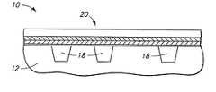
- FIG. 3is a plan view of the FIG. 1 wafer fragment at a processing step which is subsequent to that which is shown in FIG. 2, and FIG. 4 is a side view of the FIG. 3 wafer fragment.
- a transistor gate line 20is formed over respective active areas 14 , 16 to provide individual transistors, wherein the transistors corresponding to the active areas having the different active area widths have different threshold voltages as discussed above.
- Gate lines such as line 20typically have a gate oxide layer, one or more conductive layers such as polysilicon and a silicide layer, one or more insulative caps, and insulative sidewall spacers (not shown), none of which are specifically designated.
- the illustrated gate lineconstitutes a common gate line which is formed over the illustrated active areas. It is, of course, possible to form separate gate lines over the active areas having the different widths.
- two series of field effect transistorsare formed over substrate 12 .
- One of the series of field effect transistors(an exemplary transistor of which being formed over active area 14 ) is isolated from other adjacent devices by shallow trench isolation regions 18 .
- the other series of field effect transistors(an exemplary transistor of which being formed over active area 16 ) has active area widths greater than one micron, with the first-mentioned series being formed to have active area widths less than one micron to achieve lower threshold voltages than the other of the series.
- the threshold voltages for the two series of field effect transistorsare defined by one or more common channel implants. In a most preferred embodiment, the one or more common channel implants are the only implants which define the threshold voltages for the two series of field effect transistors.
- the two series of field effect transistors just mentionedinclude at least one series which is isolated from adjacent devices by shallow trench isolation regions such as regions 18 .
- Different threshold voltagesare achieved between field effect transistors in the different series by varying the active area widths of the field effect transistors in the series, with at least one of the series having active area widths less than one micron, or less for future technologies.
- field effect transistorscan be fabricated having different threshold voltages without using a separate channel implant for the field effect transistors having the different threshold voltages. Such can result in a reduction in processing steps, which formerly included additional masking steps.
- One or more of the active areascan have widths less than one micron, with such widths being varied in order to change the threshold voltages of the transistors formed thereover.
- various methods of the inventionprovide integrated circuitry having transistors with different threshold voltages without the added processing complexity.
- various methods of the inventioncan provide dynamic random access memory circuitry having a memory array area for supporting memory circuitry and a peripheral area for supporting peripheral circuitry.
- a plurality of shallow trench isolation regionsare received within the peripheral area of the substrate and define a plurality of active areas having widths within the substrate, some of the widths being no greater than about one micron. Preferably, at least two of the widths are different.
- a conductive lineis formed or disposed over the respective active areas to provide MOS gate electrodes for individual transistors.
- the transistors corresponding to the active areas having the different widthspreferably have different threshold voltages.
- Exemplary dynamic random access memory circuitryis described in U.S. Pat. Nos. 5,702,990 and 5,686,747, which are incorporated by reference.
- a circuit 28is provided and includes transistors 30 , 32 .
- Such transistorscan be fabricated, in accordance with the methods described above, to have different threshold voltages.
- transistor 30serves as a pass transistor and has a low threshold voltage V tl
- transistor 32serves as a switching transistor and has a high threshold voltage V th .
- a circuit 34is provided and includes transistors 36 , 38 which can have different threshold voltages. Such circuit comprises a portion of precharge circuitry for dynamic random access memory circuitry.
- the transistor 36has a low threshold voltage V tl and the transistor 38 has a high threshold voltage V th .
- a circuitis shown generally at 40 and comprises transistors 42 , 44 and 46 having threshold voltages V t1 , Vt 2 and Vt 3 , respectively.
- the transistors 42 , 44 and 46are fabricated to be formed in a parallel configuration with a common gate line 48 interconnecting the transistors 42 , 44 and 46 and coupling a signal C SAL to gates of the transistors.
- the transistors 42 , 44 , 46each have different active area widths which results in different threshold voltages.
- a sense amplifier circuit 50including cross-coupled transistors 52 and 54 .
- the transistors 52 and 54are formed to have a low threshold voltage V tl .
- V tlthe threshold voltage
- the circuitacts as a pull-down circuit and equilibrates the node RNL* to ground.
- Advantages of the inventioncan include provision of a plurality of transistors having different threshold voltages, without the necessity of providing different dedicated processing steps to achieve such different threshold voltages. In various preferred embodiments, such results are attained through the use of shallow trench isolation and various so-called reverse narrow width characteristics. Additionally, current drive can be achieved using multiple narrow width devices in parallel (FIG. 7). The invention can be useful for low threshold voltage applications such as precharge circuitry in DRAM circuitry, or as output drivers where low threshold voltages are important to obtain higher signal levels.
Landscapes
- Semiconductor Memories (AREA)
- Metal-Oxide And Bipolar Metal-Oxide Semiconductor Integrated Circuits (AREA)
- Non-Volatile Memory (AREA)
- Element Separation (AREA)
- Insulated Gate Type Field-Effect Transistor (AREA)
Abstract
Description
- This invention relates to semiconductor processing methods of forming transistors, to semiconductor processing methods of forming dynamic random access memory circuitry, and to related integrated circuitry.[0001]
- Semiconductor processing typically involves a number of complicated steps which include patterning, etching, and doping or implanting steps, to name just a few, which are necessary to form desired integrated circuitry. One emphasis on improving the methods through which integrated circuitry is formed, and which is directed to reducing the processing complexity, relates to reducing the number of processing steps. By reducing the number of processing steps, risks associated with processing mistakes entering into the processing flow are reduced. Additionally, wherever possible, it is also highly desirable to reduce processing complexities while providing added flexibility in the processing itself.[0002]
- For example, several processing steps are required to form transistor constructions. One or more of these steps can include a threshold voltage definition step in which one or more channel implantation steps are conducted to define the threshold voltage for the ultimately formed transistor. In some applications, it is desirable to have transistors with different threshold voltages. Typically, different threshold voltages are provided by additional masking and doping or implanting steps to adjust the doping concentration within the channel region of the various transistors desired to have the different threshold voltage. Specifically, one transistor might, be masked while another receives a threshold implant; and then other of the transistors might be masked while the first-masked transistor receives a threshold implant.[0003]
- This invention grew out of concerns associated with reducing the processing complexities involved in forming transistors having different threshold voltages.[0004]
- Semiconductor processing methods of forming transistors, semiconductor processing methods of forming dynamic random access memory circuitry, and related integrated circuitry are described. In one embodiment, active areas are formed over a substrate, with one of the active areas having a width of less than one micron. A gate line is formed over the active areas to provide transistors having different threshold voltages. Preferably, the transistors are provided with different threshold voltages without using a separate channel implant for the transistors. The transistor with the lower of the threshold voltages corresponds to the active area having the width less than one micron.[0005]
- In another embodiment, a plurality of shallow trench isolation (STI) regions are formed within a substrate and define a plurality of active areas having widths at least some of which are no greater than about one micron, with at least two of the widths preferably being different. A gate line is formed over the respective active areas to provide individual transistors, with the transistors corresponding to the active areas having the different widths having different threshold voltages. In an STI process, devices having width smaller than 1 micron typically also have a lower threshold voltage. This is referred to as “reversed narrow width effect as contrasted with the case of transistors formed using LOCOS isolation, where threshold voltage tends to increase as device width decreases.[0006]
- In another embodiment, two field effect transistors are fabricated having different threshold voltages without using a separate channel implant for one of the transistors versus the other.[0007]
- In yet another embodiment, two series of field effect transistors are formed, with one series being isolated from adjacent devices by shallow trench isolation, the other series having active area widths greater than one micron. The one series is formed to have active area widths less than one micron to achieve lower threshold voltages than the other of the series.[0008]
- In yet another embodiment, one of the two series of field effect transistors are isolated by shallow trench isolation, and different threshold voltages between the field effect transistors in different series are achieved by varying the active area widths of the field effect transistors in the series. At least one of the series preferably has active area widths less than one micron.[0009]
- Preferred embodiments of the invention are described below with reference to the following accompanying drawings.[0010]
- FIG. 1 is a diagrammatic side sectional view of the semiconductor wafer fragment in process in accordance with one embodiment of the invention.[0011]
- FIG. 2 is a view of the FIG. 1 wafer fragment at a processing step which is subsequent to that which is shown in FIG. 1.[0012]
- FIG. 3 is a plan view of the FIG. 1 wafer fragment at a processing step which is subsequent to that which is shown in FIG. 2.[0013]
- FIG. 4 is a side view of the FIG. 3 wafer fragment.[0014]
- FIG. 5 is a schematic diagram of circuitry formed in accordance with another embodiment of the invention.[0015]
- FIG. 6 is a schematic diagram of circuitry formed in accordance with another embodiment of the invention.[0016]
- FIG. 7 is a schematic diagram of circuitry formed in accordance with another embodiment of the invention.[0017]
- This disclosure of the invention is submitted in furtherance of the constitutional purposes of the U.S. Patent Laws “to promote the progress of science and useful arts” ([0018]
Article 1, Section 8). - Referring to FIG. 1, a semiconductor wafer fragment in process is shown generally at[0019]10, and includes a
semiconductive substrate 12. In the context of this document, the term “semiconductive substrate” is defined to mean any construction comprising semiconductive material, including, but not limited to, bulk semiconductive materials such as a semiconductive wafer (either alone or in assemblies comprising other materials thereon), and semiconductive material layers (either alone or in assemblies comprising other materials). The term “substrate” refers to any supporting structure, including, but not limited to, the semiconductive substrates described above. - Referring to FIG. 2, a plurality of active areas are formed over[0020]
substrate 12, with an exemplary pair ofactive areas Active areas sub-areas trench isolation regions 18 which are received withinsubstrate 12. The spacing of shallowtrench isolation regions 18 defines a plurality of active area widths, with exemplary widths being shown at w1and w2. Preferably, at least two of the widths are different from one another. Of course, more than two of the widths could be different from one another. - In one embodiment, some of the active area widths are no greater than about one micron. One micron happens to be a break point that is technologically dependent. In other words, STI transistors show a threshold voltage reduction with reducing gate width when the gate width is about one micron or less. It will be understood that other sizes that correspond to a break point in threshold voltage versus gate width or control element size for transistors made using other technologies could be used instead of “one micron”.[0021]
- In one embodiment, one or both of widths w[0022]1and w2could be less than one micron. In a preferred embodiment, the different active area widths impart to transistors which are to be formed, different threshold voltages which, in a most preferred embodiment, are achieved without conducting or using a separate channel implant for the different transistors. Such results in a reduction in the number of processing steps which were previously required to form transistors having different threshold voltages.
- In one embodiment, the different threshold voltages are each less than two volts. In another embodiment, the different threshold voltages are each less than one volt. In this example, the transistor having the lower of the threshold voltages corresponds to the transistor which is formed relative to the active area having the lesser or smaller active area width.[0023]
- With respect to provision of the channel implant(s) which defines the threshold voltages, one or more such implants can be conducted relative to the active areas. Preferably, each of the one or more channel implants are common to the transistors having the different active area widths which, in turn, provides, transistors having different threshold voltages.[0024]
- FIG. 3 is a plan view of the FIG. 1 wafer fragment at a processing step which is subsequent to that which is shown in FIG. 2, and FIG. 4 is a side view of the FIG. 3 wafer fragment. A[0025]
transistor gate line 20 is formed over respectiveactive areas line 20 typically have a gate oxide layer, one or more conductive layers such as polysilicon and a silicide layer, one or more insulative caps, and insulative sidewall spacers (not shown), none of which are specifically designated. The illustrated gate line constitutes a common gate line which is formed over the illustrated active areas. It is, of course, possible to form separate gate lines over the active areas having the different widths. - Alternately considered, and in accordance with one embodiment of the present invention, two series of field effect transistors are formed over[0026]
substrate 12. One of the series of field effect transistors (an exemplary transistor of which being formed over active area14) is isolated from other adjacent devices by shallowtrench isolation regions 18. The other series of field effect transistors (an exemplary transistor of which being formed over active area16) has active area widths greater than one micron, with the first-mentioned series being formed to have active area widths less than one micron to achieve lower threshold voltages than the other of the series. Preferably, the threshold voltages for the two series of field effect transistors are defined by one or more common channel implants. In a most preferred embodiment, the one or more common channel implants are the only implants which define the threshold voltages for the two series of field effect transistors. - Further and alternately considered, and in accordance with another embodiment of the present invention, the two series of field effect transistors just mentioned include at least one series which is isolated from adjacent devices by shallow trench isolation regions such as[0027]
regions 18. Different threshold voltages are achieved between field effect transistors in the different series by varying the active area widths of the field effect transistors in the series, with at least one of the series having active area widths less than one micron, or less for future technologies. - Accordingly, field effect transistors can be fabricated having different threshold voltages without using a separate channel implant for the field effect transistors having the different threshold voltages. Such can result in a reduction in processing steps, which formerly included additional masking steps. One or more of the active areas can have widths less than one micron, with such widths being varied in order to change the threshold voltages of the transistors formed thereover.[0028]
- In operation, various methods of the invention provide integrated circuitry having transistors with different threshold voltages without the added processing complexity. In a preferred embodiment, various methods of the invention can provide dynamic random access memory circuitry having a memory array area for supporting memory circuitry and a peripheral area for supporting peripheral circuitry. A plurality of shallow trench isolation regions are received within the peripheral area of the substrate and define a plurality of active areas having widths within the substrate, some of the widths being no greater than about one micron. Preferably, at least two of the widths are different. A conductive line is formed or disposed over the respective active areas to provide MOS gate electrodes for individual transistors. The transistors corresponding to the active areas having the different widths preferably have different threshold voltages. Exemplary dynamic random access memory circuitry is described in U.S. Pat. Nos. 5,702,990 and 5,686,747, which are incorporated by reference.[0029]
- Referring to FIG. 5, a[0030]
circuit 28 is provided and includestransistors transistor 30 serves as a pass transistor and has a low threshold voltage Vtl, whiletransistor 32 serves as a switching transistor and has a high threshold voltage Vth. - Referring to FIG. 6, a[0031]
circuit 34 is provided and includestransistors transistor 36 has a low threshold voltage Vtland thetransistor 38 has a high threshold voltage Vth. - Referring to FIG. 7, a circuit is shown generally at[0032]40 and comprises
transistors transistors common gate line 48 interconnecting thetransistors transistors - Also shown in FIG. 7 is a[0033]
sense amplifier circuit 50 includingcross-coupled transistors transistors transistors multiple transistors transistors - Advantages of the invention can include provision of a plurality of transistors having different threshold voltages, without the necessity of providing different dedicated processing steps to achieve such different threshold voltages. In various preferred embodiments, such results are attained through the use of shallow trench isolation and various so-called reverse narrow width characteristics. Additionally, current drive can be achieved using multiple narrow width devices in parallel (FIG. 7). The invention can be useful for low threshold voltage applications such as precharge circuitry in DRAM circuitry, or as output drivers where low threshold voltages are important to obtain higher signal levels.[0034]
- In compliance with the statute, the invention has been described in language more or less specific as to structural and methodical features. It is to be understood, however, that the invention is not limited to the specific features shown and described, since the means herein disclosed comprise preferred forms of putting the invention into effect. The invention is, therefore, claimed in any of its forms or modifications within the proper scope of the appended claims appropriately interpreted in accordance with the doctrine of equivalents.[0035]
Claims (50)
Priority Applications (6)
| Application Number | Priority Date | Filing Date | Title |
|---|---|---|---|
| US10/071,453US7057257B2 (en) | 1999-09-01 | 2002-02-08 | Semiconductor processing methods of forming transistors, semiconductor processing methods of forming dynamic random access memory circuitry, and related integrated circuitry |
| US10/229,650US20020195670A1 (en) | 1999-09-01 | 2002-08-27 | Semiconductor processing methods of forming transistors, semiconductor processing methods of forming dynamic random access memory circuitry, and related integrated circuitry |
| US10/931,368US6914287B2 (en) | 1999-09-01 | 2004-08-31 | Semiconductor processing methods of forming transistors, semiconductor processing methods of forming dynamic random access memory circuitry, and related integrated circuitry |
| US11/215,954US20050287733A1 (en) | 1999-09-01 | 2005-08-30 | Semiconductor processing methods of forming transistors, semiconductor processing methods of forming dynamic random access memory circuitry, and related integrated circuitry |
| US11/217,033US7291880B2 (en) | 1999-09-01 | 2005-08-31 | Transistor assembly |
| US11/216,915US7294903B2 (en) | 1999-09-01 | 2005-08-31 | Transistor assemblies |
Applications Claiming Priority (3)
| Application Number | Priority Date | Filing Date | Title |
|---|---|---|---|
| US09/388,857US7253047B2 (en) | 1999-09-01 | 1999-09-01 | Semiconductor processing methods of forming transistors, semiconductor processing methods of forming dynamic random access memory circuitry, and related integrated circuitry |
| US09/834,660US20010012664A1 (en) | 1999-09-01 | 2001-04-12 | Semiconductor processing methods of forming transistors, semiconductor processing methods of forming dynamic random access memory circuitry, and related integrated circuitry |
| US10/071,453US7057257B2 (en) | 1999-09-01 | 2002-02-08 | Semiconductor processing methods of forming transistors, semiconductor processing methods of forming dynamic random access memory circuitry, and related integrated circuitry |
Related Parent Applications (1)
| Application Number | Title | Priority Date | Filing Date |
|---|---|---|---|
| US09/834,660DivisionUS20010012664A1 (en) | 1999-09-01 | 2001-04-12 | Semiconductor processing methods of forming transistors, semiconductor processing methods of forming dynamic random access memory circuitry, and related integrated circuitry |
Related Child Applications (3)
| Application Number | Title | Priority Date | Filing Date |
|---|---|---|---|
| US10/229,650DivisionUS20020195670A1 (en) | 1999-09-01 | 2002-08-27 | Semiconductor processing methods of forming transistors, semiconductor processing methods of forming dynamic random access memory circuitry, and related integrated circuitry |
| US11/217,033DivisionUS7291880B2 (en) | 1999-09-01 | 2005-08-31 | Transistor assembly |
| US11/216,915DivisionUS7294903B2 (en) | 1999-09-01 | 2005-08-31 | Transistor assemblies |
Publications (2)
| Publication Number | Publication Date |
|---|---|
| US20020072199A1true US20020072199A1 (en) | 2002-06-13 |
| US7057257B2 US7057257B2 (en) | 2006-06-06 |
Family
ID=23535826
Family Applications (9)
| Application Number | Title | Priority Date | Filing Date |
|---|---|---|---|
| US09/388,857Expired - LifetimeUS7253047B2 (en) | 1999-09-01 | 1999-09-01 | Semiconductor processing methods of forming transistors, semiconductor processing methods of forming dynamic random access memory circuitry, and related integrated circuitry |
| US09/834,660AbandonedUS20010012664A1 (en) | 1999-09-01 | 2001-04-12 | Semiconductor processing methods of forming transistors, semiconductor processing methods of forming dynamic random access memory circuitry, and related integrated circuitry |
| US10/071,453Expired - LifetimeUS7057257B2 (en) | 1999-09-01 | 2002-02-08 | Semiconductor processing methods of forming transistors, semiconductor processing methods of forming dynamic random access memory circuitry, and related integrated circuitry |
| US10/229,650AbandonedUS20020195670A1 (en) | 1999-09-01 | 2002-08-27 | Semiconductor processing methods of forming transistors, semiconductor processing methods of forming dynamic random access memory circuitry, and related integrated circuitry |
| US10/931,368Expired - LifetimeUS6914287B2 (en) | 1999-09-01 | 2004-08-31 | Semiconductor processing methods of forming transistors, semiconductor processing methods of forming dynamic random access memory circuitry, and related integrated circuitry |
| US11/215,954AbandonedUS20050287733A1 (en) | 1999-09-01 | 2005-08-30 | Semiconductor processing methods of forming transistors, semiconductor processing methods of forming dynamic random access memory circuitry, and related integrated circuitry |
| US11/216,915Expired - LifetimeUS7294903B2 (en) | 1999-09-01 | 2005-08-31 | Transistor assemblies |
| US11/217,033Expired - LifetimeUS7291880B2 (en) | 1999-09-01 | 2005-08-31 | Transistor assembly |
| US11/218,172AbandonedUS20060008977A1 (en) | 1999-09-01 | 2005-08-31 | Semiconductor processing methods of forming transistors, semiconductor processing methods of forming dynamic random access memory circuitry, and related integrated circuitry |
Family Applications Before (2)
| Application Number | Title | Priority Date | Filing Date |
|---|---|---|---|
| US09/388,857Expired - LifetimeUS7253047B2 (en) | 1999-09-01 | 1999-09-01 | Semiconductor processing methods of forming transistors, semiconductor processing methods of forming dynamic random access memory circuitry, and related integrated circuitry |
| US09/834,660AbandonedUS20010012664A1 (en) | 1999-09-01 | 2001-04-12 | Semiconductor processing methods of forming transistors, semiconductor processing methods of forming dynamic random access memory circuitry, and related integrated circuitry |
Family Applications After (6)
| Application Number | Title | Priority Date | Filing Date |
|---|---|---|---|
| US10/229,650AbandonedUS20020195670A1 (en) | 1999-09-01 | 2002-08-27 | Semiconductor processing methods of forming transistors, semiconductor processing methods of forming dynamic random access memory circuitry, and related integrated circuitry |
| US10/931,368Expired - LifetimeUS6914287B2 (en) | 1999-09-01 | 2004-08-31 | Semiconductor processing methods of forming transistors, semiconductor processing methods of forming dynamic random access memory circuitry, and related integrated circuitry |
| US11/215,954AbandonedUS20050287733A1 (en) | 1999-09-01 | 2005-08-30 | Semiconductor processing methods of forming transistors, semiconductor processing methods of forming dynamic random access memory circuitry, and related integrated circuitry |
| US11/216,915Expired - LifetimeUS7294903B2 (en) | 1999-09-01 | 2005-08-31 | Transistor assemblies |
| US11/217,033Expired - LifetimeUS7291880B2 (en) | 1999-09-01 | 2005-08-31 | Transistor assembly |
| US11/218,172AbandonedUS20060008977A1 (en) | 1999-09-01 | 2005-08-31 | Semiconductor processing methods of forming transistors, semiconductor processing methods of forming dynamic random access memory circuitry, and related integrated circuitry |
Country Status (1)
| Country | Link |
|---|---|
| US (9) | US7253047B2 (en) |
Cited By (1)
| Publication number | Priority date | Publication date | Assignee | Title |
|---|---|---|---|---|
| US20020195670A1 (en)* | 1999-09-01 | 2002-12-26 | Tran Luan C. | Semiconductor processing methods of forming transistors, semiconductor processing methods of forming dynamic random access memory circuitry, and related integrated circuitry |
Families Citing this family (24)
| Publication number | Priority date | Publication date | Assignee | Title |
|---|---|---|---|---|
| US6583459B1 (en)* | 2000-06-30 | 2003-06-24 | Stmicroelectronics, Inc. | Random access memory cell and method for fabricating same |
| US6834019B2 (en)* | 2002-08-29 | 2004-12-21 | Micron Technology, Inc. | Isolation device over field in a memory device |
| SE0300924D0 (en)* | 2003-03-28 | 2003-03-28 | Infineon Technologies Wireless | A method to provide a triple well in an epitaxially based CMOS or BiCMOS process |
| US8519503B2 (en)* | 2006-06-05 | 2013-08-27 | Osi Optoelectronics, Inc. | High speed backside illuminated, front side contact photodiode array |
| US7576369B2 (en)* | 2005-10-25 | 2009-08-18 | Udt Sensors, Inc. | Deep diffused thin photodiodes |
| US7656001B2 (en) | 2006-11-01 | 2010-02-02 | Udt Sensors, Inc. | Front-side illuminated, back-side contact double-sided PN-junction photodiode arrays |
| US7880258B2 (en)* | 2003-05-05 | 2011-02-01 | Udt Sensors, Inc. | Thin wafer detectors with improved radiation damage and crosstalk characteristics |
| US7057254B2 (en)* | 2003-05-05 | 2006-06-06 | Udt Sensors, Inc. | Front illuminated back side contact thin wafer detectors |
| US8164151B2 (en)* | 2007-05-07 | 2012-04-24 | Osi Optoelectronics, Inc. | Thin active layer fishbone photodiode and method of manufacturing the same |
| US7709921B2 (en) | 2008-08-27 | 2010-05-04 | Udt Sensors, Inc. | Photodiode and photodiode array with improved performance characteristics |
| US8686529B2 (en) | 2010-01-19 | 2014-04-01 | Osi Optoelectronics, Inc. | Wavelength sensitive sensor photodiodes |
| US7279731B1 (en)* | 2006-05-15 | 2007-10-09 | Udt Sensors, Inc. | Edge illuminated photodiodes |
| US7141468B2 (en)* | 2003-10-27 | 2006-11-28 | Texas Instruments Incorporated | Application of different isolation schemes for logic and embedded memory |
| US7560762B2 (en)* | 2005-08-23 | 2009-07-14 | Macronix International Co., Ltd. | Asymmetric floating gate NAND flash memory |
| US7319611B2 (en)* | 2006-01-25 | 2008-01-15 | Macronix International Co., Ltd. | Bitline transistor architecture for flash memory |
| US8208233B2 (en)* | 2008-03-18 | 2012-06-26 | Mediatek Inc. | ESD protection circuit and method thereof |
| CN102217082B (en) | 2008-09-15 | 2013-12-04 | Osi光电子股份有限公司 | Thin active layer fishbone photodiode with a shallow n+ layer and method of manufacturing the same |
| US8399909B2 (en) | 2009-05-12 | 2013-03-19 | Osi Optoelectronics, Inc. | Tetra-lateral position sensing detector |
| US8461005B2 (en)* | 2010-03-03 | 2013-06-11 | United Microelectronics Corp. | Method of manufacturing doping patterns |
| US8652934B1 (en) | 2012-12-26 | 2014-02-18 | Micron Technology, Inc. | Semiconductor substrate for photonic and electronic structures and method of manufacture |
| US8912615B2 (en) | 2013-01-24 | 2014-12-16 | Osi Optoelectronics, Inc. | Shallow junction photodiode for detecting short wavelength light |
| US9006743B2 (en)* | 2013-05-13 | 2015-04-14 | Shenzhen China Star Optoelectronics Technology Co., Ltd | Thin film transistor, thin film transistor array substrate, and method for making the same |
| CN103227209B (en)* | 2013-05-13 | 2016-01-06 | 深圳市华星光电技术有限公司 | Thin-film transistor, thin-film transistor array base-plate and manufacture method thereof |
| US10290546B2 (en) | 2016-11-29 | 2019-05-14 | Taiwan Semiconductor Manufacturing Co., Ltd. | Threshold voltage adjustment for a gate-all-around semiconductor structure |
Citations (54)
| Publication number | Priority date | Publication date | Assignee | Title |
|---|---|---|---|---|
| US4987093A (en)* | 1987-04-15 | 1991-01-22 | Texas Instruments Incorporated | Through-field implant isolated devices and method |
| US5111069A (en)* | 1990-08-27 | 1992-05-05 | Dallas Semiconductor Corporation | Layout of integrated circuit with very large transistors |
| US5130268A (en)* | 1991-04-05 | 1992-07-14 | Sgs-Thomson Microelectronics, Inc. | Method for forming planarized shallow trench isolation in an integrated circuit and a structure formed thereby |
| US5422507A (en)* | 1992-10-15 | 1995-06-06 | Standard Microsystems Corporation | Electrical isolation in integrated circuits |
| US5447884A (en)* | 1994-06-29 | 1995-09-05 | International Business Machines Corporation | Shallow trench isolation with thin nitride liner |
| US5498565A (en)* | 1991-11-29 | 1996-03-12 | Sony Corporation | Method of forming trench isolation having polishing step and method of manufacturing semiconductor device |
| US5665202A (en)* | 1995-11-24 | 1997-09-09 | Motorola, Inc. | Multi-step planarization process using polishing at two different pad pressures |
| US5691215A (en)* | 1996-08-26 | 1997-11-25 | Industrial Technology Research Institute | Method for fabricating a sub-half micron MOSFET device with insulator filled shallow trenches planarized via use of negative photoresist and de-focus exposure |
| US5702976A (en)* | 1995-10-24 | 1997-12-30 | Micron Technology, Inc. | Shallow trench isolation using low dielectric constant insulator |
| US5717635A (en)* | 1996-08-27 | 1998-02-10 | International Business Machines Corporation | High density EEPROM for solid state file |
| US5721173A (en)* | 1997-02-25 | 1998-02-24 | Kabushiki Kaisha Toshiba | Method of forming a shallow trench isolation structure |
| US5721172A (en)* | 1996-12-02 | 1998-02-24 | Taiwan Semiconductor Manufacturing Company, Ltd. | Self-aligned polish stop layer hard masking method for forming planarized aperture fill layers |
| US5728621A (en)* | 1997-04-28 | 1998-03-17 | Chartered Semiconductor Manufacturing Pte Ltd | Method for shallow trench isolation |
| US5732014A (en)* | 1997-02-20 | 1998-03-24 | Micron Technology, Inc. | Merged transistor structure for gain memory cell |
| US5811347A (en)* | 1996-04-29 | 1998-09-22 | Advanced Micro Devices, Inc. | Nitrogenated trench liner for improved shallow trench isolation |
| US5817567A (en)* | 1997-04-07 | 1998-10-06 | Taiwan Semiconductor Manufacturing Company Ltd. | Shallow trench isolation method |
| US5821591A (en)* | 1996-02-02 | 1998-10-13 | Siemens Aktiengesellschaft | High density read only memory cell configuration and method for its production |
| US5851899A (en)* | 1996-08-08 | 1998-12-22 | Siemens Aktiengesellschaft | Gapfill and planarization process for shallow trench isolation |
| US5851900A (en)* | 1997-04-28 | 1998-12-22 | Mosel Vitelic Inc. | Method of manufacturing a shallow trench isolation for a semiconductor device |
| US5866934A (en)* | 1997-06-20 | 1999-02-02 | Advanced Micro Devices, Inc. | Parallel and series-coupled transistors having gate conductors formed on sidewall surfaces of a sacrificial structure |
| US5869396A (en)* | 1996-07-15 | 1999-02-09 | Chartered Semiconductor Manufacturing Ltd. | Method for forming a polycide gate electrode |
| US5872043A (en)* | 1996-07-25 | 1999-02-16 | Industrial Technology Research Institute | Method of planarizing wafers with shallow trench isolation |
| US5880007A (en)* | 1997-09-30 | 1999-03-09 | Siemens Aktiengesellschaft | Planarization of a non-conformal device layer in semiconductor fabrication |
| US5920276A (en)* | 1996-03-11 | 1999-07-06 | Imaging Accessories, Inc. | Automatic horizontal and vertical scanning radar with terrain display |
| US5923993A (en)* | 1997-12-17 | 1999-07-13 | Advanced Micro Devices | Method for fabricating dishing free shallow isolation trenches |
| US5950091A (en)* | 1996-12-06 | 1999-09-07 | Advanced Micro Devices, Inc. | Method of making a polysilicon gate conductor of an integrated circuit formed as a sidewall spacer on a sacrificial material |
| US6009023A (en)* | 1998-05-26 | 1999-12-28 | Etron Technology, Inc. | High performance DRAM structure employing multiple thickness gate oxide |
| US6048775A (en)* | 1999-05-24 | 2000-04-11 | Vanguard International Semiconductor Corporation | Method to make shallow trench isolation structure by HDP-CVD and chemical mechanical polish processes |
| US6048771A (en)* | 1998-04-27 | 2000-04-11 | United Microelectronics Corp. | Shallow trench isolation technique |
| US6057207A (en)* | 1998-03-25 | 2000-05-02 | Taiwan Semiconductor Manufacturing Company | Shallow trench isolation process using chemical-mechanical polish with self-aligned nitride mask on HDP-oxide |
| US6057210A (en)* | 1998-04-21 | 2000-05-02 | Vanguard International Semiconductor Corporation | Method of making a shallow trench isolation for ULSI formation via in-direct CMP process |
| US6071792A (en)* | 1997-04-30 | 2000-06-06 | Samsung Electronics Co., Ltd. | Methods of forming shallow trench isolation regions using plasma deposition techniques |
| US6124183A (en)* | 1997-12-18 | 2000-09-26 | Advanced Micro Devices, Inc. | Shallow trench isolation formation with simplified reverse planarization mask |
| US6133098A (en)* | 1999-05-17 | 2000-10-17 | Halo Lsi Design & Device Technology, Inc. | Process for making and programming and operating a dual-bit multi-level ballistic flash memory |
| US6159822A (en)* | 1999-06-02 | 2000-12-12 | Vanguard International Semiconductor Corporation | Self-planarized shallow trench isolation |
| US6191446B1 (en)* | 1998-03-04 | 2001-02-20 | Advanced Micro Devices, Inc. | Formation and control of a vertically oriented transistor channel length |
| US6228713B1 (en)* | 1999-06-28 | 2001-05-08 | Chartered Semiconductor Manufacturing Ltd. | Self-aligned floating gate for memory application using shallow trench isolation |
| US6261914B1 (en)* | 1999-07-27 | 2001-07-17 | International Business Machines Corporation | Process for improving local uniformity of chemical mechanical polishing using a self-aligned polish rate enhancement layer |
| US20010012664A1 (en)* | 1999-09-01 | 2001-08-09 | Tran Luan C. | Semiconductor processing methods of forming transistors, semiconductor processing methods of forming dynamic random access memory circuitry, and related integrated circuitry |
| US6278295B1 (en)* | 1998-02-10 | 2001-08-21 | Cypress Semiconductor Corp. | Buffer with stable trip point |
| US6281082B1 (en)* | 2000-03-13 | 2001-08-28 | Chartered Semiconductor Manufacturing Ltd. | Method to form MOS transistors with a common shallow trench isolation and interlevel dielectric gap fill |
| US20010020724A1 (en)* | 1998-10-15 | 2001-09-13 | Wayne S. Berry | Structure and method for dual gate oxidation for cmos technology |
| US6329251B1 (en)* | 2000-08-10 | 2001-12-11 | Taiwan Semiconductor Manufacturing Company, Ltd | Microelectronic fabrication method employing self-aligned selectively deposited silicon layer |
| US20020020106A1 (en)* | 1999-07-07 | 2002-02-21 | Filippini Brian B. | Amino alkylphenol emulsifiers for an aqueous hydrocarbon fuel |
| US6426534B1 (en)* | 2000-05-01 | 2002-07-30 | Xilinx, Inc. | Methods and circuits employing threshold voltages for mask-alignment detection |
| US6436751B1 (en)* | 2001-02-13 | 2002-08-20 | United Microelectronics Corp. | Fabrication method and structure of a flash memory |
| US6492693B2 (en)* | 1998-08-12 | 2002-12-10 | Micron Technology, Inc. | Low voltage high performance semiconductor devices and methods |
| US6501114B2 (en)* | 2000-03-03 | 2002-12-31 | Micron Technology, Inc. | Structures comprising transistor gates |
| US6545904B2 (en)* | 2001-03-16 | 2003-04-08 | Micron Technology, Inc. | 6f2 dram array, a dram array formed on a semiconductive substrate, a method of forming memory cells in a 6f2 dram array and a method of isolating a single row of memory cells in a 6f2 dram array |
| US6620704B2 (en)* | 1993-07-02 | 2003-09-16 | Hitachi, Ltd. | Method of fabricating low stress semiconductor devices with thermal oxide isolation |
| US6649461B1 (en)* | 2002-04-25 | 2003-11-18 | Chartered Semiconductor Manufacturing Ltd. | Method of angle implant to improve transistor reverse narrow width effect |
| US6734487B2 (en)* | 1997-04-22 | 2004-05-11 | Micron Technology, Inc. | Memory integrated circuitry with DRAMs using LOCOS isolations and areas less than 6F2 |
| US20040188777A1 (en)* | 2003-03-31 | 2004-09-30 | Macronix International Co., Ltd. | Mixed signal embedded mask ROM with virtual ground array and method for manufacturing same |
| US6834019B2 (en)* | 2002-08-29 | 2004-12-21 | Micron Technology, Inc. | Isolation device over field in a memory device |
Family Cites Families (58)
| Publication number | Priority date | Publication date | Assignee | Title |
|---|---|---|---|---|
| BE622939A (en)* | 1961-09-28 | |||
| US3191446A (en)* | 1964-01-21 | 1965-06-29 | Sarkes Tarzian | Fine tuning mechanism for television tuners |
| EP0169271B1 (en)* | 1984-06-26 | 1988-06-15 | Tandberg Data A/S | Stand for a video display unit adjustable in height |
| US4943537A (en) | 1988-06-23 | 1990-07-24 | Dallas Semiconductor Corporation | CMOS integrated circuit with reduced susceptibility to PMOS punchthrough |
| US5407849A (en) | 1992-06-23 | 1995-04-18 | Imp, Inc. | CMOS process and circuit including zero threshold transistors |
| US5329251A (en)* | 1993-04-28 | 1994-07-12 | National Semiconductor Corporation | Multiple biasing phase-lock-loops controlling center frequency of phase-lock-loop clock recovery circuit |
| US5492858A (en)* | 1994-04-20 | 1996-02-20 | Digital Equipment Corporation | Shallow trench isolation process for high aspect ratio trenches |
| US6246449B1 (en)* | 1996-08-16 | 2001-06-12 | Rosen Products Llc | Display unit |
| JPH10144886A (en) | 1996-09-11 | 1998-05-29 | Toshiba Corp | Semiconductor device and manufacturing method thereof |
| US5926723A (en) | 1997-03-04 | 1999-07-20 | Advanced Micro Devices, Inc. | Generation of a loose planarization mask having relaxed boundary conditions for use in shallow trench isolation processes |
| JP3638778B2 (en) | 1997-03-31 | 2005-04-13 | 株式会社ルネサステクノロジ | Semiconductor integrated circuit device and manufacturing method thereof |
| US5892707A (en) | 1997-04-25 | 1999-04-06 | Micron Technology, Inc. | Memory array having a digit line buried in an isolation region and method for forming same |
| TW332915B (en) | 1997-06-24 | 1998-06-01 | Ti Acer Co Ltd | The producing method for shallow trench isolation with global planarization |
| US6556435B1 (en)* | 1997-10-31 | 2003-04-29 | Hewlett-Packard Company | Adjustable height docking station and computing device for use therewith |
| US6236079B1 (en) | 1997-12-02 | 2001-05-22 | Kabushiki Kaisha Toshiba | Dynamic semiconductor memory device having a trench capacitor |
| US5994178A (en) | 1997-12-31 | 1999-11-30 | Texas Instruments - Acer Incorporated | Method of fabricating CMOS transistors with a planar shallow trench isolation |
| JP3344311B2 (en)* | 1998-02-23 | 2002-11-11 | 株式会社タツノ・メカトロニクス | Gate type car wash machine |
| US5994198A (en) | 1998-02-23 | 1999-11-30 | International Business Machines Corporation | Fabrication method for fully landing subminimum features on minimum width lines |
| US6353242B1 (en) | 1998-03-30 | 2002-03-05 | Kabushiki Kaisha Toshiba | Nonvolatile semiconductor memory |
| US6028784A (en) | 1998-05-01 | 2000-02-22 | Texas Instruments Incorporated | Ferroelectric memory device having compact memory cell array |
| US6048765A (en) | 1998-06-03 | 2000-04-11 | Texas Instruments - Acer Incorporated | Method of forming high density buried bit line flash EEPROM memory cell with a shallow trench floating gate |
| US6153467A (en) | 1998-06-03 | 2000-11-28 | Texas Instruments - Acer Incorporated | Method of fabricating high density buried bit line flash EEPROM memory cell with a shallow trench floating gate |
| US6156620A (en) | 1998-07-22 | 2000-12-05 | Lsi Logic Corporation | Isolation trench in semiconductor substrate with nitrogen-containing barrier region, and process for forming same |
| US6121651A (en) | 1998-07-30 | 2000-09-19 | International Business Machines Corporation | Dram cell with three-sided-gate transfer device |
| US6468855B2 (en) | 1998-08-14 | 2002-10-22 | Monolithic System Technology, Inc. | Reduced topography DRAM cell fabricated using a modified logic process and method for operating same |
| US6573548B2 (en) | 1998-08-14 | 2003-06-03 | Monolithic System Technology, Inc. | DRAM cell having a capacitor structure fabricated partially in a cavity and method for operating same |
| US6509595B1 (en) | 1999-06-14 | 2003-01-21 | Monolithic System Technology, Inc. | DRAM cell fabricated using a modified logic process and method for operating same |
| US6265282B1 (en)* | 1998-08-17 | 2001-07-24 | Micron Technology, Inc. | Process for making an isolation structure |
| KR100308072B1 (en)* | 1998-08-27 | 2001-10-19 | 박종섭 | Manufacturing method of semiconductor device |
| US6121078A (en) | 1998-09-17 | 2000-09-19 | International Business Machines Corporation | Integrated circuit planarization and fill biasing design method |
| US5960276A (en)* | 1998-09-28 | 1999-09-28 | Taiwan Semiconductor Manufacturing Company, Ltd. | Using an extra boron implant to improve the NMOS reverse narrow width effect in shallow trench isolation process |
| US6037671A (en) | 1998-11-03 | 2000-03-14 | Advanced Micro Devices, Inc. | Stepper alignment mark structure for maintaining alignment integrity |
| US6309942B1 (en) | 1999-02-04 | 2001-10-30 | Advanced Micro Devices, Inc. | STI punch-through defects and stress reduction by high temperature oxide reflow process |
| US6133055A (en) | 1999-05-21 | 2000-10-17 | United Semiconductor Corp | Method of forming a test key architecture |
| US6171929B1 (en)* | 1999-06-22 | 2001-01-09 | Vanguard International Semiconductor Corporation | Shallow trench isolator via non-critical chemical mechanical polishing |
| US6297082B1 (en) | 1999-08-25 | 2001-10-02 | United Microelectronics Corp. | Method of fabricating a MOS transistor with local channel ion implantation regions |
| US6391756B1 (en) | 1999-08-31 | 2002-05-21 | Micron Technology, Inc. | Semiconductor processing methods of forming contact openings |
| US6259601B1 (en)* | 1999-09-30 | 2001-07-10 | Dell Usa, L.P. | Apparatus for providing docking station assisted cooling of a portable computer |
| US6177324B1 (en) | 1999-10-28 | 2001-01-23 | Chartered Semiconductor Manufacturing, Ltd. | ESD protection device for STI deep submicron technology |
| US6339455B1 (en)* | 1999-12-29 | 2002-01-15 | William L. Allan | Digital video disc vehicle television |
| US6509695B2 (en)* | 2000-04-27 | 2003-01-21 | Canon Kabushiki Kaisha | Flash apparatus and camera having the flash apparatus |
| US20010048404A1 (en)* | 2000-05-23 | 2001-12-06 | Rosen Products Llc. | Ceiling mounted monitor system |
| US6420749B1 (en) | 2000-06-23 | 2002-07-16 | International Business Machines Corporation | Trench field shield in trench isolation |
| US6411553B1 (en)* | 2000-08-31 | 2002-06-25 | Micron Technology, Inc. | Single ended data bus equilibration scheme |
| US6403484B1 (en)* | 2001-03-12 | 2002-06-11 | Chartered Semiconductor Manufacturing Ltd. | Method to achieve STI planarization |
| US6411555B1 (en) | 2001-03-19 | 2002-06-25 | Micron Technology, Inc. | Reference charge generator, a method for providing a reference charge from a reference charge generator, a method of operating a reference charge generator and a dram memory circuit formed using memory cells having an area of 6f2 |
| US6429081B1 (en) | 2001-05-17 | 2002-08-06 | Taiwan Semiconductor Manufacturing Company | Parasitic surface transfer transistor cell (PASTT cell) for bi-level and multi-level NAND flash memory |
| US6606543B1 (en)* | 2002-01-09 | 2003-08-12 | Microsoft Corporation | Method and apparatus for logging into a vehicle computer system |
| US6856030B2 (en) | 2002-07-08 | 2005-02-15 | Viciciv Technology | Semiconductor latches and SRAM devices |
| US6758441B2 (en)* | 2002-07-25 | 2004-07-06 | The Boeing Company | Store ejection system with replaceable pressure vessel |
| US6871356B2 (en)* | 2002-10-28 | 2005-03-22 | Johnson Safety, Inc. | Mobile video system |
| US7050124B2 (en)* | 2002-11-05 | 2006-05-23 | Samsung Electronics Co., Ltd. | Mobile video system |
| US7071515B2 (en)* | 2003-07-14 | 2006-07-04 | Taiwan Semiconductor Manufacturing Co., Ltd. | Narrow width effect improvement with photoresist plug process and STI corner ion implantation |
| US6949785B2 (en)* | 2004-01-14 | 2005-09-27 | Taiwan Semiconductor Manufacturing Co., Ltd. | Random access memory (RAM) capacitor in shallow trench isolation with improved electrical isolation to overlying gate electrodes |
| US6902975B2 (en) | 2003-10-15 | 2005-06-07 | Taiwan Semiconductor Manufacturing Company, Ltd. | Non-volatile memory technology compatible with 1T-RAM process |
| US7845506B2 (en)* | 2004-04-28 | 2010-12-07 | Keith Stratton Willows | Bottle, retaining device and associated elements for carrying containers and other items |
| US7227228B2 (en)* | 2004-05-21 | 2007-06-05 | Kabushika Kaisha Toshiba | Silicon on insulator device and method of manufacturing the same |
| US7020020B1 (en)* | 2004-09-21 | 2006-03-28 | Atmel Corporation | Low voltage non-volatile memory cells using twin bit line current sensing |
- 1999
- 1999-09-01USUS09/388,857patent/US7253047B2/ennot_activeExpired - Lifetime
- 2001
- 2001-04-12USUS09/834,660patent/US20010012664A1/ennot_activeAbandoned
- 2002
- 2002-02-08USUS10/071,453patent/US7057257B2/ennot_activeExpired - Lifetime
- 2002-08-27USUS10/229,650patent/US20020195670A1/ennot_activeAbandoned
- 2004
- 2004-08-31USUS10/931,368patent/US6914287B2/ennot_activeExpired - Lifetime
- 2005
- 2005-08-30USUS11/215,954patent/US20050287733A1/ennot_activeAbandoned
- 2005-08-31USUS11/216,915patent/US7294903B2/ennot_activeExpired - Lifetime
- 2005-08-31USUS11/217,033patent/US7291880B2/ennot_activeExpired - Lifetime
- 2005-08-31USUS11/218,172patent/US20060008977A1/ennot_activeAbandoned
Patent Citations (61)
| Publication number | Priority date | Publication date | Assignee | Title |
|---|---|---|---|---|
| US4987093A (en)* | 1987-04-15 | 1991-01-22 | Texas Instruments Incorporated | Through-field implant isolated devices and method |
| US5111069A (en)* | 1990-08-27 | 1992-05-05 | Dallas Semiconductor Corporation | Layout of integrated circuit with very large transistors |
| US5130268A (en)* | 1991-04-05 | 1992-07-14 | Sgs-Thomson Microelectronics, Inc. | Method for forming planarized shallow trench isolation in an integrated circuit and a structure formed thereby |
| US5410176A (en)* | 1991-04-05 | 1995-04-25 | Sgs-Thomson Microelectronics, Inc. | Integrated circuit with planarized shallow trench isolation |
| US5498565A (en)* | 1991-11-29 | 1996-03-12 | Sony Corporation | Method of forming trench isolation having polishing step and method of manufacturing semiconductor device |
| US5422507A (en)* | 1992-10-15 | 1995-06-06 | Standard Microsystems Corporation | Electrical isolation in integrated circuits |
| US20040214355A1 (en)* | 1993-07-02 | 2004-10-28 | Hideo Miura | Semiconductor memory device |
| US6620704B2 (en)* | 1993-07-02 | 2003-09-16 | Hitachi, Ltd. | Method of fabricating low stress semiconductor devices with thermal oxide isolation |
| US5447884A (en)* | 1994-06-29 | 1995-09-05 | International Business Machines Corporation | Shallow trench isolation with thin nitride liner |
| US5702976A (en)* | 1995-10-24 | 1997-12-30 | Micron Technology, Inc. | Shallow trench isolation using low dielectric constant insulator |
| US5665202A (en)* | 1995-11-24 | 1997-09-09 | Motorola, Inc. | Multi-step planarization process using polishing at two different pad pressures |
| US6180458B1 (en)* | 1996-02-02 | 2001-01-30 | Infineon Technologies Ag | Method of producing a memory cell configuration |
| US5821591A (en)* | 1996-02-02 | 1998-10-13 | Siemens Aktiengesellschaft | High density read only memory cell configuration and method for its production |
| US5920276A (en)* | 1996-03-11 | 1999-07-06 | Imaging Accessories, Inc. | Automatic horizontal and vertical scanning radar with terrain display |
| US5811347A (en)* | 1996-04-29 | 1998-09-22 | Advanced Micro Devices, Inc. | Nitrogenated trench liner for improved shallow trench isolation |
| US5869396A (en)* | 1996-07-15 | 1999-02-09 | Chartered Semiconductor Manufacturing Ltd. | Method for forming a polycide gate electrode |
| US5872043A (en)* | 1996-07-25 | 1999-02-16 | Industrial Technology Research Institute | Method of planarizing wafers with shallow trench isolation |
| US5851899A (en)* | 1996-08-08 | 1998-12-22 | Siemens Aktiengesellschaft | Gapfill and planarization process for shallow trench isolation |
| US5691215A (en)* | 1996-08-26 | 1997-11-25 | Industrial Technology Research Institute | Method for fabricating a sub-half micron MOSFET device with insulator filled shallow trenches planarized via use of negative photoresist and de-focus exposure |
| US5717635A (en)* | 1996-08-27 | 1998-02-10 | International Business Machines Corporation | High density EEPROM for solid state file |
| US5721172A (en)* | 1996-12-02 | 1998-02-24 | Taiwan Semiconductor Manufacturing Company, Ltd. | Self-aligned polish stop layer hard masking method for forming planarized aperture fill layers |
| US5950091A (en)* | 1996-12-06 | 1999-09-07 | Advanced Micro Devices, Inc. | Method of making a polysilicon gate conductor of an integrated circuit formed as a sidewall spacer on a sacrificial material |
| US5732014A (en)* | 1997-02-20 | 1998-03-24 | Micron Technology, Inc. | Merged transistor structure for gain memory cell |
| US5897351A (en)* | 1997-02-20 | 1999-04-27 | Micron Technology, Inc. | Method for forming merged transistor structure for gain memory cell |
| US5721173A (en)* | 1997-02-25 | 1998-02-24 | Kabushiki Kaisha Toshiba | Method of forming a shallow trench isolation structure |
| US5817567A (en)* | 1997-04-07 | 1998-10-06 | Taiwan Semiconductor Manufacturing Company Ltd. | Shallow trench isolation method |
| US6734487B2 (en)* | 1997-04-22 | 2004-05-11 | Micron Technology, Inc. | Memory integrated circuitry with DRAMs using LOCOS isolations and areas less than 6F2 |
| US5728621A (en)* | 1997-04-28 | 1998-03-17 | Chartered Semiconductor Manufacturing Pte Ltd | Method for shallow trench isolation |
| US5851900A (en)* | 1997-04-28 | 1998-12-22 | Mosel Vitelic Inc. | Method of manufacturing a shallow trench isolation for a semiconductor device |
| US6071792A (en)* | 1997-04-30 | 2000-06-06 | Samsung Electronics Co., Ltd. | Methods of forming shallow trench isolation regions using plasma deposition techniques |
| US5866934A (en)* | 1997-06-20 | 1999-02-02 | Advanced Micro Devices, Inc. | Parallel and series-coupled transistors having gate conductors formed on sidewall surfaces of a sacrificial structure |
| US6001740A (en)* | 1997-09-30 | 1999-12-14 | Siemens Aktiengesellschaft | Planarization of a non-conformal device layer in semiconductor fabrication |
| US5880007A (en)* | 1997-09-30 | 1999-03-09 | Siemens Aktiengesellschaft | Planarization of a non-conformal device layer in semiconductor fabrication |
| US5923993A (en)* | 1997-12-17 | 1999-07-13 | Advanced Micro Devices | Method for fabricating dishing free shallow isolation trenches |
| US6124183A (en)* | 1997-12-18 | 2000-09-26 | Advanced Micro Devices, Inc. | Shallow trench isolation formation with simplified reverse planarization mask |
| US6278295B1 (en)* | 1998-02-10 | 2001-08-21 | Cypress Semiconductor Corp. | Buffer with stable trip point |
| US6191446B1 (en)* | 1998-03-04 | 2001-02-20 | Advanced Micro Devices, Inc. | Formation and control of a vertically oriented transistor channel length |
| US6057207A (en)* | 1998-03-25 | 2000-05-02 | Taiwan Semiconductor Manufacturing Company | Shallow trench isolation process using chemical-mechanical polish with self-aligned nitride mask on HDP-oxide |
| US6057210A (en)* | 1998-04-21 | 2000-05-02 | Vanguard International Semiconductor Corporation | Method of making a shallow trench isolation for ULSI formation via in-direct CMP process |
| US6048771A (en)* | 1998-04-27 | 2000-04-11 | United Microelectronics Corp. | Shallow trench isolation technique |
| US6009023A (en)* | 1998-05-26 | 1999-12-28 | Etron Technology, Inc. | High performance DRAM structure employing multiple thickness gate oxide |
| US6492693B2 (en)* | 1998-08-12 | 2002-12-10 | Micron Technology, Inc. | Low voltage high performance semiconductor devices and methods |
| US20010020724A1 (en)* | 1998-10-15 | 2001-09-13 | Wayne S. Berry | Structure and method for dual gate oxidation for cmos technology |
| US6674134B2 (en)* | 1998-10-15 | 2004-01-06 | International Business Machines Corporation | Structure and method for dual gate oxidation for CMOS technology |
| US6133098A (en)* | 1999-05-17 | 2000-10-17 | Halo Lsi Design & Device Technology, Inc. | Process for making and programming and operating a dual-bit multi-level ballistic flash memory |
| US6048775A (en)* | 1999-05-24 | 2000-04-11 | Vanguard International Semiconductor Corporation | Method to make shallow trench isolation structure by HDP-CVD and chemical mechanical polish processes |
| US6159822A (en)* | 1999-06-02 | 2000-12-12 | Vanguard International Semiconductor Corporation | Self-planarized shallow trench isolation |
| US6228713B1 (en)* | 1999-06-28 | 2001-05-08 | Chartered Semiconductor Manufacturing Ltd. | Self-aligned floating gate for memory application using shallow trench isolation |
| US20020020106A1 (en)* | 1999-07-07 | 2002-02-21 | Filippini Brian B. | Amino alkylphenol emulsifiers for an aqueous hydrocarbon fuel |
| US6261914B1 (en)* | 1999-07-27 | 2001-07-17 | International Business Machines Corporation | Process for improving local uniformity of chemical mechanical polishing using a self-aligned polish rate enhancement layer |
| US20010012664A1 (en)* | 1999-09-01 | 2001-08-09 | Tran Luan C. | Semiconductor processing methods of forming transistors, semiconductor processing methods of forming dynamic random access memory circuitry, and related integrated circuitry |
| US6501114B2 (en)* | 2000-03-03 | 2002-12-31 | Micron Technology, Inc. | Structures comprising transistor gates |
| US6770927B2 (en)* | 2000-03-03 | 2004-08-03 | Micron Technology, Inc. | Structures comprising transistor gates |
| US6281082B1 (en)* | 2000-03-13 | 2001-08-28 | Chartered Semiconductor Manufacturing Ltd. | Method to form MOS transistors with a common shallow trench isolation and interlevel dielectric gap fill |
| US6426534B1 (en)* | 2000-05-01 | 2002-07-30 | Xilinx, Inc. | Methods and circuits employing threshold voltages for mask-alignment detection |
| US6329251B1 (en)* | 2000-08-10 | 2001-12-11 | Taiwan Semiconductor Manufacturing Company, Ltd | Microelectronic fabrication method employing self-aligned selectively deposited silicon layer |
| US6436751B1 (en)* | 2001-02-13 | 2002-08-20 | United Microelectronics Corp. | Fabrication method and structure of a flash memory |
| US6545904B2 (en)* | 2001-03-16 | 2003-04-08 | Micron Technology, Inc. | 6f2 dram array, a dram array formed on a semiconductive substrate, a method of forming memory cells in a 6f2 dram array and a method of isolating a single row of memory cells in a 6f2 dram array |
| US6649461B1 (en)* | 2002-04-25 | 2003-11-18 | Chartered Semiconductor Manufacturing Ltd. | Method of angle implant to improve transistor reverse narrow width effect |
| US6834019B2 (en)* | 2002-08-29 | 2004-12-21 | Micron Technology, Inc. | Isolation device over field in a memory device |
| US20040188777A1 (en)* | 2003-03-31 | 2004-09-30 | Macronix International Co., Ltd. | Mixed signal embedded mask ROM with virtual ground array and method for manufacturing same |
Cited By (11)
| Publication number | Priority date | Publication date | Assignee | Title |
|---|---|---|---|---|
| US20020195670A1 (en)* | 1999-09-01 | 2002-12-26 | Tran Luan C. | Semiconductor processing methods of forming transistors, semiconductor processing methods of forming dynamic random access memory circuitry, and related integrated circuitry |
| US20030020106A1 (en)* | 1999-09-01 | 2003-01-30 | Luan C. Tran | Semiconductor processing methods of forming transistors, semiconductor processing methods of forming dynamic random access memory circuitry, and related integrated circuitry |
| US20050029599A1 (en)* | 1999-09-01 | 2005-02-10 | Tran Luan C. | Semiconductor processing methods of forming transistors, semiconductor processing methods of forming dynamic random access memory circuitry, and related integrated circuitry |
| US6914287B2 (en)* | 1999-09-01 | 2005-07-05 | Micron Technology, Inc | Semiconductor processing methods of forming transistors, semiconductor processing methods of forming dynamic random access memory circuitry, and related integrated circuitry |
| US20050287733A1 (en)* | 1999-09-01 | 2005-12-29 | Tran Luan C | Semiconductor processing methods of forming transistors, semiconductor processing methods of forming dynamic random access memory circuitry, and related integrated circuitry |
| US20050285201A1 (en)* | 1999-09-01 | 2005-12-29 | Tran Luan C | Semiconductor processing methods of forming transistors, semiconductor processing methods of forming dynamic random access memory circuitry, and related integrated circuitry |
| US20050285163A1 (en)* | 1999-09-01 | 2005-12-29 | Tran Luan C | Semiconductor processing methods of forming transistors, semiconductor processing methods of forming dynamic random access memory circuitry, and related integrated circuitry |
| US20060008977A1 (en)* | 1999-09-01 | 2006-01-12 | Tran Luan C | Semiconductor processing methods of forming transistors, semiconductor processing methods of forming dynamic random access memory circuitry, and related integrated circuitry |
| US7253047B2 (en)* | 1999-09-01 | 2007-08-07 | Micron Technology, Inc. | Semiconductor processing methods of forming transistors, semiconductor processing methods of forming dynamic random access memory circuitry, and related integrated circuitry |
| US7291880B2 (en)* | 1999-09-01 | 2007-11-06 | Micron Technology, Inc. | Transistor assembly |
| US7294903B2 (en)* | 1999-09-01 | 2007-11-13 | Micron Technology, Inc. | Transistor assemblies |
Also Published As
| Publication number | Publication date |
|---|---|
| US7294903B2 (en) | 2007-11-13 |
| US20060008977A1 (en) | 2006-01-12 |
| US6914287B2 (en) | 2005-07-05 |
| US20050287733A1 (en) | 2005-12-29 |
| US20010012664A1 (en) | 2001-08-09 |
| US20050029599A1 (en) | 2005-02-10 |
| US7253047B2 (en) | 2007-08-07 |
| US20050285201A1 (en) | 2005-12-29 |
| US7291880B2 (en) | 2007-11-06 |
| US20050285163A1 (en) | 2005-12-29 |
| US7057257B2 (en) | 2006-06-06 |
| US20020195670A1 (en) | 2002-12-26 |
| US20030020106A1 (en) | 2003-01-30 |
Similar Documents
| Publication | Publication Date | Title |
|---|---|---|
| US7294903B2 (en) | Transistor assemblies | |
| US6107134A (en) | High performance DRAM structure employing multiple thickness gate oxide | |
| US6703673B2 (en) | SOI DRAM having P-doped poly gate for a memory pass transistor | |
| JP2001352077A (en) | SOI field effect transistor | |
| US20060211207A1 (en) | Semiconductor processing methods of forming integrated circuitry | |
| JP2000332132A (en) | Body-switched SOI (silicon on insulator) circuit and method of forming the same | |
| US5336914A (en) | Static semiconductor memory device | |
| US6281088B1 (en) | Method of manufacturing SRAM having enhanced cell ratio | |
| CN100424885C (en) | Logic switch and circuit using same | |
| US20050176193A1 (en) | Method of forming a gate of a semiconductor device | |
| US6261886B1 (en) | Increased gate to body coupling and application to DRAM and dynamic circuits | |
| US6674105B2 (en) | Semiconductor memory device and method of forming the same | |
| US6509595B1 (en) | DRAM cell fabricated using a modified logic process and method for operating same | |
| KR960012055B1 (en) | Semiconductor integrated circuit device and manufacturing method | |
| JP3082073B2 (en) | SRAM cell and method of manufacturing the same | |
| JP2882185B2 (en) | Static semiconductor memory device | |
| US5079604A (en) | SOI layout for low resistance gate | |
| JPH05175462A (en) | Semiconductor memory device |
Legal Events
| Date | Code | Title | Description |
|---|---|---|---|
| FEPP | Fee payment procedure | Free format text:PAYOR NUMBER ASSIGNED (ORIGINAL EVENT CODE: ASPN); ENTITY STATUS OF PATENT OWNER: LARGE ENTITY | |
| STCF | Information on status: patent grant | Free format text:PATENTED CASE | |
| CC | Certificate of correction | ||
| FPAY | Fee payment | Year of fee payment:4 | |
| FPAY | Fee payment | Year of fee payment:8 | |
| AS | Assignment | Owner name:U.S. BANK NATIONAL ASSOCIATION, AS COLLATERAL AGENT, CALIFORNIA Free format text:SECURITY INTEREST;ASSIGNOR:MICRON TECHNOLOGY, INC.;REEL/FRAME:038669/0001 Effective date:20160426 Owner name:U.S. BANK NATIONAL ASSOCIATION, AS COLLATERAL AGEN Free format text:SECURITY INTEREST;ASSIGNOR:MICRON TECHNOLOGY, INC.;REEL/FRAME:038669/0001 Effective date:20160426 | |
| AS | Assignment | Owner name:MORGAN STANLEY SENIOR FUNDING, INC., AS COLLATERAL AGENT, MARYLAND Free format text:PATENT SECURITY AGREEMENT;ASSIGNOR:MICRON TECHNOLOGY, INC.;REEL/FRAME:038954/0001 Effective date:20160426 Owner name:MORGAN STANLEY SENIOR FUNDING, INC., AS COLLATERAL Free format text:PATENT SECURITY AGREEMENT;ASSIGNOR:MICRON TECHNOLOGY, INC.;REEL/FRAME:038954/0001 Effective date:20160426 | |
| AS | Assignment | Owner name:U.S. BANK NATIONAL ASSOCIATION, AS COLLATERAL AGENT, CALIFORNIA Free format text:CORRECTIVE ASSIGNMENT TO CORRECT THE REPLACE ERRONEOUSLY FILED PATENT #7358718 WITH THE CORRECT PATENT #7358178 PREVIOUSLY RECORDED ON REEL 038669 FRAME 0001. ASSIGNOR(S) HEREBY CONFIRMS THE SECURITY INTEREST;ASSIGNOR:MICRON TECHNOLOGY, INC.;REEL/FRAME:043079/0001 Effective date:20160426 Owner name:U.S. BANK NATIONAL ASSOCIATION, AS COLLATERAL AGEN Free format text:CORRECTIVE ASSIGNMENT TO CORRECT THE REPLACE ERRONEOUSLY FILED PATENT #7358718 WITH THE CORRECT PATENT #7358178 PREVIOUSLY RECORDED ON REEL 038669 FRAME 0001. ASSIGNOR(S) HEREBY CONFIRMS THE SECURITY INTEREST;ASSIGNOR:MICRON TECHNOLOGY, INC.;REEL/FRAME:043079/0001 Effective date:20160426 | |
| MAFP | Maintenance fee payment | Free format text:PAYMENT OF MAINTENANCE FEE, 12TH YEAR, LARGE ENTITY (ORIGINAL EVENT CODE: M1553) Year of fee payment:12 | |
| AS | Assignment | Owner name:JPMORGAN CHASE BANK, N.A., AS COLLATERAL AGENT, ILLINOIS Free format text:SECURITY INTEREST;ASSIGNORS:MICRON TECHNOLOGY, INC.;MICRON SEMICONDUCTOR PRODUCTS, INC.;REEL/FRAME:047540/0001 Effective date:20180703 Owner name:JPMORGAN CHASE BANK, N.A., AS COLLATERAL AGENT, IL Free format text:SECURITY INTEREST;ASSIGNORS:MICRON TECHNOLOGY, INC.;MICRON SEMICONDUCTOR PRODUCTS, INC.;REEL/FRAME:047540/0001 Effective date:20180703 | |
| AS | Assignment | Owner name:MICRON TECHNOLOGY, INC., IDAHO Free format text:RELEASE BY SECURED PARTY;ASSIGNOR:U.S. BANK NATIONAL ASSOCIATION, AS COLLATERAL AGENT;REEL/FRAME:047243/0001 Effective date:20180629 | |
| AS | Assignment | Owner name:MICRON TECHNOLOGY, INC., IDAHO Free format text:RELEASE BY SECURED PARTY;ASSIGNOR:MORGAN STANLEY SENIOR FUNDING, INC., AS COLLATERAL AGENT;REEL/FRAME:050937/0001 Effective date:20190731 | |
| AS | Assignment | Owner name:MICRON TECHNOLOGY, INC., IDAHO Free format text:RELEASE BY SECURED PARTY;ASSIGNOR:JPMORGAN CHASE BANK, N.A., AS COLLATERAL AGENT;REEL/FRAME:051028/0001 Effective date:20190731 Owner name:MICRON SEMICONDUCTOR PRODUCTS, INC., IDAHO Free format text:RELEASE BY SECURED PARTY;ASSIGNOR:JPMORGAN CHASE BANK, N.A., AS COLLATERAL AGENT;REEL/FRAME:051028/0001 Effective date:20190731 |