US20020072150A1 - Process for providing electrical connection between a semiconductor die and a semiconductor die receiving member - Google Patents
Process for providing electrical connection between a semiconductor die and a semiconductor die receiving memberDownload PDFInfo
- Publication number
- US20020072150A1 US20020072150A1US10/056,350US5635002AUS2002072150A1US 20020072150 A1US20020072150 A1US 20020072150A1US 5635002 AUS5635002 AUS 5635002AUS 2002072150 A1US2002072150 A1US 2002072150A1
- Authority
- US
- United States
- Prior art keywords
- semiconductor die
- receiving member
- die receiving
- contact sites
- face
- Prior art date
- Legal status (The legal status is an assumption and is not a legal conclusion. Google has not performed a legal analysis and makes no representation as to the accuracy of the status listed.)
- Granted
Links
- 239000004065semiconductorSubstances0.000titleclaimsabstractdescription215
- 238000000034methodMethods0.000titleclaimsdescription25
- 239000000758substrateSubstances0.000claimsabstractdescription59
- 239000004020conductorSubstances0.000claimsdescription9
- 239000000853adhesiveSubstances0.000claimsdescription5
- 230000001070adhesive effectEffects0.000claimsdescription5
- 239000012790adhesive layerSubstances0.000claimsdescription5
- 239000000463materialSubstances0.000description9
- XUIMIQQOPSSXEZ-UHFFFAOYSA-NSiliconChemical compound[Si]XUIMIQQOPSSXEZ-UHFFFAOYSA-N0.000description6
- 238000004806packaging method and processMethods0.000description6
- 229910052710siliconInorganic materials0.000description6
- 239000010703siliconSubstances0.000description6
- 230000000712assemblyEffects0.000description5
- 238000000429assemblyMethods0.000description5
- 230000009977dual effectEffects0.000description3
- 239000010410layerSubstances0.000description3
- PNEYBMLMFCGWSK-UHFFFAOYSA-NAluminaChemical compound[O-2].[O-2].[O-2].[Al+3].[Al+3]PNEYBMLMFCGWSK-UHFFFAOYSA-N0.000description2
- 239000000919ceramicSubstances0.000description2
- 239000011152fibreglassSubstances0.000description2
- 239000012212insulatorSubstances0.000description2
- 238000007639printingMethods0.000description2
- 229910052594sapphireInorganic materials0.000description2
- 239000010980sapphireSubstances0.000description2
- 229910000679solderInorganic materials0.000description2
- 238000004891communicationMethods0.000description1
- 229920001940conductive polymerPolymers0.000description1
- 238000010276constructionMethods0.000description1
- 239000003989dielectric materialSubstances0.000description1
- 230000000694effectsEffects0.000description1
- 238000005516engineering processMethods0.000description1
- 230000006870functionEffects0.000description1
- 238000004519manufacturing processMethods0.000description1
- 239000002184metalSubstances0.000description1
- 238000012858packaging processMethods0.000description1
- 230000000135prohibitive effectEffects0.000description1
Images


Classifications
- H—ELECTRICITY
- H01—ELECTRIC ELEMENTS
- H01L—SEMICONDUCTOR DEVICES NOT COVERED BY CLASS H10
- H01L23/00—Details of semiconductor or other solid state devices
- H01L23/52—Arrangements for conducting electric current within the device in operation from one component to another, i.e. interconnections, e.g. wires, lead frames
- H01L23/538—Arrangements for conducting electric current within the device in operation from one component to another, i.e. interconnections, e.g. wires, lead frames the interconnection structure between a plurality of semiconductor chips being formed on, or in, insulating substrates
- H01L23/5382—Adaptable interconnections, e.g. for engineering changes
- H—ELECTRICITY
- H01—ELECTRIC ELEMENTS
- H01L—SEMICONDUCTOR DEVICES NOT COVERED BY CLASS H10
- H01L23/00—Details of semiconductor or other solid state devices
- H01L23/48—Arrangements for conducting electric current to or from the solid state body in operation, e.g. leads, terminal arrangements ; Selection of materials therefor
- H01L23/488—Arrangements for conducting electric current to or from the solid state body in operation, e.g. leads, terminal arrangements ; Selection of materials therefor consisting of soldered or bonded constructions
- H01L23/498—Leads, i.e. metallisations or lead-frames on insulating substrates, e.g. chip carriers
- H01L23/49838—Geometry or layout
- H—ELECTRICITY
- H01—ELECTRIC ELEMENTS
- H01L—SEMICONDUCTOR DEVICES NOT COVERED BY CLASS H10
- H01L24/00—Arrangements for connecting or disconnecting semiconductor or solid-state bodies; Methods or apparatus related thereto
- H01L24/01—Means for bonding being attached to, or being formed on, the surface to be connected, e.g. chip-to-package, die-attach, "first-level" interconnects; Manufacturing methods related thereto
- H01L24/10—Bump connectors ; Manufacturing methods related thereto
- H01L24/15—Structure, shape, material or disposition of the bump connectors after the connecting process
- H01L24/16—Structure, shape, material or disposition of the bump connectors after the connecting process of an individual bump connector
- H—ELECTRICITY
- H01—ELECTRIC ELEMENTS
- H01L—SEMICONDUCTOR DEVICES NOT COVERED BY CLASS H10
- H01L24/00—Arrangements for connecting or disconnecting semiconductor or solid-state bodies; Methods or apparatus related thereto
- H01L24/01—Means for bonding being attached to, or being formed on, the surface to be connected, e.g. chip-to-package, die-attach, "first-level" interconnects; Manufacturing methods related thereto
- H01L24/42—Wire connectors; Manufacturing methods related thereto
- H01L24/47—Structure, shape, material or disposition of the wire connectors after the connecting process
- H01L24/48—Structure, shape, material or disposition of the wire connectors after the connecting process of an individual wire connector
- H—ELECTRICITY
- H01—ELECTRIC ELEMENTS
- H01L—SEMICONDUCTOR DEVICES NOT COVERED BY CLASS H10
- H01L2224/00—Indexing scheme for arrangements for connecting or disconnecting semiconductor or solid-state bodies and methods related thereto as covered by H01L24/00
- H01L2224/01—Means for bonding being attached to, or being formed on, the surface to be connected, e.g. chip-to-package, die-attach, "first-level" interconnects; Manufacturing methods related thereto
- H01L2224/02—Bonding areas; Manufacturing methods related thereto
- H01L2224/04—Structure, shape, material or disposition of the bonding areas prior to the connecting process
- H01L2224/0401—Bonding areas specifically adapted for bump connectors, e.g. under bump metallisation [UBM]
- H—ELECTRICITY
- H01—ELECTRIC ELEMENTS
- H01L—SEMICONDUCTOR DEVICES NOT COVERED BY CLASS H10
- H01L2224/00—Indexing scheme for arrangements for connecting or disconnecting semiconductor or solid-state bodies and methods related thereto as covered by H01L24/00
- H01L2224/01—Means for bonding being attached to, or being formed on, the surface to be connected, e.g. chip-to-package, die-attach, "first-level" interconnects; Manufacturing methods related thereto
- H01L2224/02—Bonding areas; Manufacturing methods related thereto
- H01L2224/04—Structure, shape, material or disposition of the bonding areas prior to the connecting process
- H01L2224/05—Structure, shape, material or disposition of the bonding areas prior to the connecting process of an individual bonding area
- H01L2224/0554—External layer
- H01L2224/0555—Shape
- H01L2224/05552—Shape in top view
- H01L2224/05554—Shape in top view being square
- H—ELECTRICITY
- H01—ELECTRIC ELEMENTS
- H01L—SEMICONDUCTOR DEVICES NOT COVERED BY CLASS H10
- H01L2224/00—Indexing scheme for arrangements for connecting or disconnecting semiconductor or solid-state bodies and methods related thereto as covered by H01L24/00
- H01L2224/01—Means for bonding being attached to, or being formed on, the surface to be connected, e.g. chip-to-package, die-attach, "first-level" interconnects; Manufacturing methods related thereto
- H01L2224/02—Bonding areas; Manufacturing methods related thereto
- H01L2224/04—Structure, shape, material or disposition of the bonding areas prior to the connecting process
- H01L2224/05—Structure, shape, material or disposition of the bonding areas prior to the connecting process of an individual bonding area
- H01L2224/0554—External layer
- H01L2224/05599—Material
- H—ELECTRICITY
- H01—ELECTRIC ELEMENTS
- H01L—SEMICONDUCTOR DEVICES NOT COVERED BY CLASS H10
- H01L2224/00—Indexing scheme for arrangements for connecting or disconnecting semiconductor or solid-state bodies and methods related thereto as covered by H01L24/00
- H01L2224/01—Means for bonding being attached to, or being formed on, the surface to be connected, e.g. chip-to-package, die-attach, "first-level" interconnects; Manufacturing methods related thereto
- H01L2224/10—Bump connectors; Manufacturing methods related thereto
- H01L2224/12—Structure, shape, material or disposition of the bump connectors prior to the connecting process
- H01L2224/13—Structure, shape, material or disposition of the bump connectors prior to the connecting process of an individual bump connector
- H01L2224/13001—Core members of the bump connector
- H01L2224/13099—Material
- H—ELECTRICITY
- H01—ELECTRIC ELEMENTS
- H01L—SEMICONDUCTOR DEVICES NOT COVERED BY CLASS H10
- H01L2224/00—Indexing scheme for arrangements for connecting or disconnecting semiconductor or solid-state bodies and methods related thereto as covered by H01L24/00
- H01L2224/01—Means for bonding being attached to, or being formed on, the surface to be connected, e.g. chip-to-package, die-attach, "first-level" interconnects; Manufacturing methods related thereto
- H01L2224/10—Bump connectors; Manufacturing methods related thereto
- H01L2224/15—Structure, shape, material or disposition of the bump connectors after the connecting process
- H01L2224/16—Structure, shape, material or disposition of the bump connectors after the connecting process of an individual bump connector
- H01L2224/161—Disposition
- H01L2224/16151—Disposition the bump connector connecting between a semiconductor or solid-state body and an item not being a semiconductor or solid-state body, e.g. chip-to-substrate, chip-to-passive
- H01L2224/16221—Disposition the bump connector connecting between a semiconductor or solid-state body and an item not being a semiconductor or solid-state body, e.g. chip-to-substrate, chip-to-passive the body and the item being stacked
- H01L2224/16225—Disposition the bump connector connecting between a semiconductor or solid-state body and an item not being a semiconductor or solid-state body, e.g. chip-to-substrate, chip-to-passive the body and the item being stacked the item being non-metallic, e.g. insulating substrate with or without metallisation
- H01L2224/16235—Disposition the bump connector connecting between a semiconductor or solid-state body and an item not being a semiconductor or solid-state body, e.g. chip-to-substrate, chip-to-passive the body and the item being stacked the item being non-metallic, e.g. insulating substrate with or without metallisation the bump connector connecting to a via metallisation of the item
- H—ELECTRICITY
- H01—ELECTRIC ELEMENTS
- H01L—SEMICONDUCTOR DEVICES NOT COVERED BY CLASS H10
- H01L2224/00—Indexing scheme for arrangements for connecting or disconnecting semiconductor or solid-state bodies and methods related thereto as covered by H01L24/00
- H01L2224/01—Means for bonding being attached to, or being formed on, the surface to be connected, e.g. chip-to-package, die-attach, "first-level" interconnects; Manufacturing methods related thereto
- H01L2224/26—Layer connectors, e.g. plate connectors, solder or adhesive layers; Manufacturing methods related thereto
- H01L2224/31—Structure, shape, material or disposition of the layer connectors after the connecting process
- H01L2224/32—Structure, shape, material or disposition of the layer connectors after the connecting process of an individual layer connector
- H01L2224/321—Disposition
- H01L2224/32151—Disposition the layer connector connecting between a semiconductor or solid-state body and an item not being a semiconductor or solid-state body, e.g. chip-to-substrate, chip-to-passive
- H01L2224/32221—Disposition the layer connector connecting between a semiconductor or solid-state body and an item not being a semiconductor or solid-state body, e.g. chip-to-substrate, chip-to-passive the body and the item being stacked
- H01L2224/32225—Disposition the layer connector connecting between a semiconductor or solid-state body and an item not being a semiconductor or solid-state body, e.g. chip-to-substrate, chip-to-passive the body and the item being stacked the item being non-metallic, e.g. insulating substrate with or without metallisation
- H—ELECTRICITY
- H01—ELECTRIC ELEMENTS
- H01L—SEMICONDUCTOR DEVICES NOT COVERED BY CLASS H10
- H01L2224/00—Indexing scheme for arrangements for connecting or disconnecting semiconductor or solid-state bodies and methods related thereto as covered by H01L24/00
- H01L2224/01—Means for bonding being attached to, or being formed on, the surface to be connected, e.g. chip-to-package, die-attach, "first-level" interconnects; Manufacturing methods related thereto
- H01L2224/42—Wire connectors; Manufacturing methods related thereto
- H01L2224/47—Structure, shape, material or disposition of the wire connectors after the connecting process
- H01L2224/48—Structure, shape, material or disposition of the wire connectors after the connecting process of an individual wire connector
- H01L2224/4805—Shape
- H01L2224/4809—Loop shape
- H01L2224/48091—Arched
- H—ELECTRICITY
- H01—ELECTRIC ELEMENTS
- H01L—SEMICONDUCTOR DEVICES NOT COVERED BY CLASS H10
- H01L2224/00—Indexing scheme for arrangements for connecting or disconnecting semiconductor or solid-state bodies and methods related thereto as covered by H01L24/00
- H01L2224/01—Means for bonding being attached to, or being formed on, the surface to be connected, e.g. chip-to-package, die-attach, "first-level" interconnects; Manufacturing methods related thereto
- H01L2224/42—Wire connectors; Manufacturing methods related thereto
- H01L2224/47—Structure, shape, material or disposition of the wire connectors after the connecting process
- H01L2224/48—Structure, shape, material or disposition of the wire connectors after the connecting process of an individual wire connector
- H01L2224/481—Disposition
- H01L2224/48151—Connecting between a semiconductor or solid-state body and an item not being a semiconductor or solid-state body, e.g. chip-to-substrate, chip-to-passive
- H01L2224/48221—Connecting between a semiconductor or solid-state body and an item not being a semiconductor or solid-state body, e.g. chip-to-substrate, chip-to-passive the body and the item being stacked
- H01L2224/48225—Connecting between a semiconductor or solid-state body and an item not being a semiconductor or solid-state body, e.g. chip-to-substrate, chip-to-passive the body and the item being stacked the item being non-metallic, e.g. insulating substrate with or without metallisation
- H01L2224/48227—Connecting between a semiconductor or solid-state body and an item not being a semiconductor or solid-state body, e.g. chip-to-substrate, chip-to-passive the body and the item being stacked the item being non-metallic, e.g. insulating substrate with or without metallisation connecting the wire to a bond pad of the item
- H—ELECTRICITY
- H01—ELECTRIC ELEMENTS
- H01L—SEMICONDUCTOR DEVICES NOT COVERED BY CLASS H10
- H01L2224/00—Indexing scheme for arrangements for connecting or disconnecting semiconductor or solid-state bodies and methods related thereto as covered by H01L24/00
- H01L2224/01—Means for bonding being attached to, or being formed on, the surface to be connected, e.g. chip-to-package, die-attach, "first-level" interconnects; Manufacturing methods related thereto
- H01L2224/42—Wire connectors; Manufacturing methods related thereto
- H01L2224/47—Structure, shape, material or disposition of the wire connectors after the connecting process
- H01L2224/48—Structure, shape, material or disposition of the wire connectors after the connecting process of an individual wire connector
- H01L2224/481—Disposition
- H01L2224/48151—Connecting between a semiconductor or solid-state body and an item not being a semiconductor or solid-state body, e.g. chip-to-substrate, chip-to-passive
- H01L2224/48221—Connecting between a semiconductor or solid-state body and an item not being a semiconductor or solid-state body, e.g. chip-to-substrate, chip-to-passive the body and the item being stacked
- H01L2224/48225—Connecting between a semiconductor or solid-state body and an item not being a semiconductor or solid-state body, e.g. chip-to-substrate, chip-to-passive the body and the item being stacked the item being non-metallic, e.g. insulating substrate with or without metallisation
- H01L2224/48235—Connecting between a semiconductor or solid-state body and an item not being a semiconductor or solid-state body, e.g. chip-to-substrate, chip-to-passive the body and the item being stacked the item being non-metallic, e.g. insulating substrate with or without metallisation connecting the wire to a via metallisation of the item
- H—ELECTRICITY
- H01—ELECTRIC ELEMENTS
- H01L—SEMICONDUCTOR DEVICES NOT COVERED BY CLASS H10
- H01L2224/00—Indexing scheme for arrangements for connecting or disconnecting semiconductor or solid-state bodies and methods related thereto as covered by H01L24/00
- H01L2224/01—Means for bonding being attached to, or being formed on, the surface to be connected, e.g. chip-to-package, die-attach, "first-level" interconnects; Manufacturing methods related thereto
- H01L2224/42—Wire connectors; Manufacturing methods related thereto
- H01L2224/47—Structure, shape, material or disposition of the wire connectors after the connecting process
- H01L2224/48—Structure, shape, material or disposition of the wire connectors after the connecting process of an individual wire connector
- H01L2224/484—Connecting portions
- H—ELECTRICITY
- H01—ELECTRIC ELEMENTS
- H01L—SEMICONDUCTOR DEVICES NOT COVERED BY CLASS H10
- H01L2224/00—Indexing scheme for arrangements for connecting or disconnecting semiconductor or solid-state bodies and methods related thereto as covered by H01L24/00
- H01L2224/73—Means for bonding being of different types provided for in two or more of groups H01L2224/10, H01L2224/18, H01L2224/26, H01L2224/34, H01L2224/42, H01L2224/50, H01L2224/63, H01L2224/71
- H01L2224/732—Location after the connecting process
- H01L2224/73251—Location after the connecting process on different surfaces
- H01L2224/73265—Layer and wire connectors
- H—ELECTRICITY
- H01—ELECTRIC ELEMENTS
- H01L—SEMICONDUCTOR DEVICES NOT COVERED BY CLASS H10
- H01L2224/00—Indexing scheme for arrangements for connecting or disconnecting semiconductor or solid-state bodies and methods related thereto as covered by H01L24/00
- H01L2224/80—Methods for connecting semiconductor or other solid state bodies using means for bonding being attached to, or being formed on, the surface to be connected
- H01L2224/85—Methods for connecting semiconductor or other solid state bodies using means for bonding being attached to, or being formed on, the surface to be connected using a wire connector
- H01L2224/8538—Bonding interfaces outside the semiconductor or solid-state body
- H01L2224/85399—Material
- H—ELECTRICITY
- H01—ELECTRIC ELEMENTS
- H01L—SEMICONDUCTOR DEVICES NOT COVERED BY CLASS H10
- H01L2924/00—Indexing scheme for arrangements or methods for connecting or disconnecting semiconductor or solid-state bodies as covered by H01L24/00
- H01L2924/0001—Technical content checked by a classifier
- H01L2924/00014—Technical content checked by a classifier the subject-matter covered by the group, the symbol of which is combined with the symbol of this group, being disclosed without further technical details
- H—ELECTRICITY
- H01—ELECTRIC ELEMENTS
- H01L—SEMICONDUCTOR DEVICES NOT COVERED BY CLASS H10
- H01L2924/00—Indexing scheme for arrangements or methods for connecting or disconnecting semiconductor or solid-state bodies as covered by H01L24/00
- H01L2924/01—Chemical elements
- H01L2924/01014—Silicon [Si]
- H—ELECTRICITY
- H01—ELECTRIC ELEMENTS
- H01L—SEMICONDUCTOR DEVICES NOT COVERED BY CLASS H10
- H01L2924/00—Indexing scheme for arrangements or methods for connecting or disconnecting semiconductor or solid-state bodies as covered by H01L24/00
- H01L2924/01—Chemical elements
- H01L2924/01027—Cobalt [Co]
- H—ELECTRICITY
- H01—ELECTRIC ELEMENTS
- H01L—SEMICONDUCTOR DEVICES NOT COVERED BY CLASS H10
- H01L2924/00—Indexing scheme for arrangements or methods for connecting or disconnecting semiconductor or solid-state bodies as covered by H01L24/00
- H01L2924/013—Alloys
- H01L2924/014—Solder alloys
- H—ELECTRICITY
- H01—ELECTRIC ELEMENTS
- H01L—SEMICONDUCTOR DEVICES NOT COVERED BY CLASS H10
- H01L2924/00—Indexing scheme for arrangements or methods for connecting or disconnecting semiconductor or solid-state bodies as covered by H01L24/00
- H01L2924/10—Details of semiconductor or other solid state devices to be connected
- H01L2924/1015—Shape
- H01L2924/1016—Shape being a cuboid
- H01L2924/10161—Shape being a cuboid with a rectangular active surface
- H—ELECTRICITY
- H01—ELECTRIC ELEMENTS
- H01L—SEMICONDUCTOR DEVICES NOT COVERED BY CLASS H10
- H01L2924/00—Indexing scheme for arrangements or methods for connecting or disconnecting semiconductor or solid-state bodies as covered by H01L24/00
- H01L2924/10—Details of semiconductor or other solid state devices to be connected
- H01L2924/102—Material of the semiconductor or solid state bodies
- H01L2924/1025—Semiconducting materials
- H01L2924/10251—Elemental semiconductors, i.e. Group IV
- H01L2924/10253—Silicon [Si]
- H—ELECTRICITY
- H01—ELECTRIC ELEMENTS
- H01L—SEMICONDUCTOR DEVICES NOT COVERED BY CLASS H10
- H01L2924/00—Indexing scheme for arrangements or methods for connecting or disconnecting semiconductor or solid-state bodies as covered by H01L24/00
- H01L2924/10—Details of semiconductor or other solid state devices to be connected
- H01L2924/11—Device type
- H01L2924/14—Integrated circuits
- H—ELECTRICITY
- H01—ELECTRIC ELEMENTS
- H01L—SEMICONDUCTOR DEVICES NOT COVERED BY CLASS H10
- H01L2924/00—Indexing scheme for arrangements or methods for connecting or disconnecting semiconductor or solid-state bodies as covered by H01L24/00
- H01L2924/15—Details of package parts other than the semiconductor or other solid state devices to be connected
- H01L2924/151—Die mounting substrate
- H01L2924/1517—Multilayer substrate
- H01L2924/15172—Fan-out arrangement of the internal vias
- H01L2924/15174—Fan-out arrangement of the internal vias in different layers of the multilayer substrate
- H—ELECTRICITY
- H01—ELECTRIC ELEMENTS
- H01L—SEMICONDUCTOR DEVICES NOT COVERED BY CLASS H10
- H01L2924/00—Indexing scheme for arrangements or methods for connecting or disconnecting semiconductor or solid-state bodies as covered by H01L24/00
- H01L2924/15—Details of package parts other than the semiconductor or other solid state devices to be connected
- H01L2924/151—Die mounting substrate
- H01L2924/1517—Multilayer substrate
- H01L2924/15192—Resurf arrangement of the internal vias
- H—ELECTRICITY
- H01—ELECTRIC ELEMENTS
- H01L—SEMICONDUCTOR DEVICES NOT COVERED BY CLASS H10
- H01L2924/00—Indexing scheme for arrangements or methods for connecting or disconnecting semiconductor or solid-state bodies as covered by H01L24/00
- H01L2924/15—Details of package parts other than the semiconductor or other solid state devices to be connected
- H01L2924/151—Die mounting substrate
- H01L2924/153—Connection portion
- H01L2924/1531—Connection portion the connection portion being formed only on the surface of the substrate opposite to the die mounting surface
- H01L2924/15311—Connection portion the connection portion being formed only on the surface of the substrate opposite to the die mounting surface being a ball array, e.g. BGA
- Y—GENERAL TAGGING OF NEW TECHNOLOGICAL DEVELOPMENTS; GENERAL TAGGING OF CROSS-SECTIONAL TECHNOLOGIES SPANNING OVER SEVERAL SECTIONS OF THE IPC; TECHNICAL SUBJECTS COVERED BY FORMER USPC CROSS-REFERENCE ART COLLECTIONS [XRACs] AND DIGESTS
- Y10—TECHNICAL SUBJECTS COVERED BY FORMER USPC
- Y10T—TECHNICAL SUBJECTS COVERED BY FORMER US CLASSIFICATION
- Y10T156/00—Adhesive bonding and miscellaneous chemical manufacture
- Y10T156/10—Methods of surface bonding and/or assembly therefor
- Y—GENERAL TAGGING OF NEW TECHNOLOGICAL DEVELOPMENTS; GENERAL TAGGING OF CROSS-SECTIONAL TECHNOLOGIES SPANNING OVER SEVERAL SECTIONS OF THE IPC; TECHNICAL SUBJECTS COVERED BY FORMER USPC CROSS-REFERENCE ART COLLECTIONS [XRACs] AND DIGESTS
- Y10—TECHNICAL SUBJECTS COVERED BY FORMER USPC
- Y10T—TECHNICAL SUBJECTS COVERED BY FORMER US CLASSIFICATION
- Y10T29/00—Metal working
- Y10T29/49—Method of mechanical manufacture
- Y10T29/49002—Electrical device making
- Y10T29/49117—Conductor or circuit manufacturing
- Y10T29/49124—On flat or curved insulated base, e.g., printed circuit, etc.
- Y10T29/4913—Assembling to base an electrical component, e.g., capacitor, etc.
- Y—GENERAL TAGGING OF NEW TECHNOLOGICAL DEVELOPMENTS; GENERAL TAGGING OF CROSS-SECTIONAL TECHNOLOGIES SPANNING OVER SEVERAL SECTIONS OF THE IPC; TECHNICAL SUBJECTS COVERED BY FORMER USPC CROSS-REFERENCE ART COLLECTIONS [XRACs] AND DIGESTS
- Y10—TECHNICAL SUBJECTS COVERED BY FORMER USPC
- Y10T—TECHNICAL SUBJECTS COVERED BY FORMER US CLASSIFICATION
- Y10T29/00—Metal working
- Y10T29/53—Means to assemble or disassemble
- Y10T29/5313—Means to assemble electrical device
- Y10T29/53174—Means to fasten electrical component to wiring board, base, or substrate
- Y10T29/53178—Chip component
Definitions
- a semiconductor package assemblyis provided that is configured to accept or include either of a flip-chip or a wirebond semiconductor die.
- a receiving memberis capable of receiving a semiconductor die in either a flip-chip or wirebond orientation.
- the assemblyincludes the receiving member attached to a semiconductor die in either the flip-chip or wirebond orientation.
Landscapes
- Engineering & Computer Science (AREA)
- Computer Hardware Design (AREA)
- Microelectronics & Electronic Packaging (AREA)
- Power Engineering (AREA)
- Physics & Mathematics (AREA)
- Condensed Matter Physics & Semiconductors (AREA)
- General Physics & Mathematics (AREA)
- Geometry (AREA)
- Wire Bonding (AREA)
Abstract
Description
- This is a divisional of U.S. patent application Ser. No. 09/060,740, filed on Apr. 15, 1998, which is incorporated herein by reference.[0001]
- The present invention relates to semiconductor chip packaging. More particularly, the present invention relates to semiconductor package assemblies configured to accept both flip-chip and wirebond semiconductor chips.[0002]
- Integrated circuits are currently manufactured by an elaborate process in which semiconductor devices, insulating films, and patterned conducting films are sequentially constructed in a predetermined arrangement on a semiconductor substrate. In the context of this document, the term “semiconductor substrate” is defined to mean any construction comprising semiconductive material, including but not limited to bulk semiconductive material such as a semiconductive wafer, either alone or in assemblies comprising other materials thereon, and semiconductive material layers, either alone or in assemblies comprising other materials. The term “substrate” refers to any supporting structure including but not limited to the semiconductor substrates described above. The term “electronic component” refers to any device or structure which may be connected to and respond to an electrical power or signal source, and includes, but is not limited to, semiconductor dies, semiconductor substrates, and integrated circuits as described above.[0003]
- Semiconductor dies are commonly packaged to produce devices in a form for convenient use by consumers. Packaging steps are conducted to provide signal and power distribution to and from the semiconductor die, to dissipate heat from the semiconductor die, and to physically protect the semiconductor die. There is an ongoing effort in the semiconductor industry to reduce packaging costs, to improve electrical and thermal performance, and to reduce size.[0004]
- An important packaging process is that of mounting and electrically connecting a semiconductor die to a mounting substrate such as a printed circuit board. A printed circuit board has a series of internal and external printed wires for electrically connecting two or more semiconductor dies or other electronic components that are mounted or attached thereto. Commonly, a semiconductor die is mounted over a receiving member that is in turn attached to the mounting substrate. Often, the receiving member is also a printed circuit board. The receiving member has a series of internal electrically conductive traces, each of which extends between at least two contact sites. One contact site is positioned to provide electrical connection with a bond pad on the semiconductor die, while the other contact site is located so as to provide electrical connection with the mounting substrate. Thus, a semiconductor package assembly formed according to the above-described process includes a semiconductor die mounted over a receiving member, which is in turn attached to a mounting substrate.[0005]
- Semiconductor dies are structured according to one of at least two available designs: wirebond and flip-chip. Wirebond semiconductor dies have a set of bond pads arrayed on a face thereof. These semiconductor dies are packaged on a mounting substrate such that the face having the bond pads faces away from the receiving member and the mounting substrate. The bond pads are then wired to corresponding contact sites on the receiving member. In contrast, the bond pads of a flip-chip semiconductor die are arrayed on the opposite face. The face of a flip-chip that has the bond pads is disposed directly on the receiving member. An array of solder balls or other conductive material provides electrical connection between the bond pads of the flip-chip and the contact sites of the receiving member.[0006]
- Manufacturers may find it commercially desirable to produce any specific integrated circuit according to both the wirebond and flip-chip designs. For example, one customer may demand a flip-chip, while another customer may be satisfied with a wirebond semiconductor die. However, such dual design of integrated circuits has required two corresponding receiving members, one configured to receive a flip-chip, and the other to receive the wirebond semiconductor die. Dual design of receiving members is expensive for the manufacturer—it requires increased inventory and redundant design and effort. The cost of producing and keeping in inventory dual receiving members may make production of dually designed integrated circuits prohibitive, thereby preventing market demand from being satisfied. It will be appreciated that a receiving member that is capable of receiving either a flip-chip or a wirebond semiconductor die, as needed, would be advantageous.[0007]
- The present invention is directed to a semiconductor package assembly that is configured to include or receive either a flip-chip or a wirebond semiconductor die. According to the invention, one receiving member design is sufficient to provide packaging for both the flip-chip and wirebond designs of a semiconductor die. Thus, a single receiving member can be used with either a flip-chip or wirebond semiconductor die according to customer demand or other design constraints. Various embodiments of the invention include a receiving member alone or a receiving member in combination with one or both of a mounting substrate and an electronic component.[0008]
- The receiving member according to the invention has a component receiving surface with a component receiving region thereon. The component receiving region is configured to receive an electronic component. The component receiving region is defined and bounded by a perimeter that corresponds to the periphery of the electronic component. Accordingly, an electronic component mounted over a component receiving surface will be aligned with and substantially positioned over the component receiving region.[0009]
- According to a preferred embodiment of the invention, a plurality of first contact sites and a plurality of second contact sites are arrayed on the component receiving surface. The first contact sites are positioned within the perimeter of the component receiving region, and provide electrical connection with the bond pads of a flip-chip. The second contact sites are positioned outside of the perimeter, and provide electrical connection with the bond pads of a wirebond electronic component. Electrically conductive traces within the receiving member connect the first contact sites and the second contact sites with terminal contact sites positioned on a surface of the receiving member. Each trace connects one corresponding first contact site, one corresponding second contact site, and one corresponding terminal contact site.[0010]
- In order to illustrate the manner in which the above-recited and other advantages and features of the invention are obtained, a more particular description of the invention briefly described above will be rendered by reference to specific embodiments thereof which are illustrated in the appended drawings. Understanding that these drawings depict only typical embodiments of the invention and are therefore not to be considered limiting of its scope, the invention will be described with additional specificity and detail through the use of the accompanying drawings in which:[0011]
- FIG. 1 is a top view of a receiving member configured for receiving an electronic component.[0012]
- FIG. 2 is a top view of another receiving member configured for receiving an electronic component.[0013]
- FIG. 3 is a top view of the receiving member of either FIG. 1 or FIG. 2, wherein a plurality of first contact sites and a plurality of second contact sites are replaced with contact sites that may be used with either wirebond or flip-chip components.[0014]
- FIG. 4 is a cross section elevation view of the receiving member of FIG. 1.[0015]
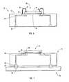
- FIG. 5 is a cross section elevation view of a semiconductor package assembly including the receiving member of FIG. 1 in combination with an electronic component in the flip-chip orientation.[0016]
- FIG. 6 is a cross section elevation view of a semiconductor package assembly including the receiving member of FIG. 1 in combination with an electronic component in the wirebond orientation.[0017]
- FIG. 7 is a cross section elevation view of the semiconductor package assembly of FIG. 5 attached to a mounting substrate.[0018]
- FIG. 8 is a cross section elevation view of a semiconductor package assembly including the receiving member of FIG. 2 in combination with an electronic component and attached to a mounting substrate.[0019]
- According to the present invention, a semiconductor package assembly is provided that is configured to accept or include either of a flip-chip or a wirebond semiconductor die. In one embodiment of the invention, a receiving member is capable of receiving a semiconductor die in either a flip-chip or wirebond orientation. In a further embodiment, the assembly includes the receiving member attached to a semiconductor die in either the flip-chip or wirebond orientation.[0020]
- Shown in FIG. 1 is a semiconductor die receiving[0021]
member 10 in a first embodiment. Semiconductor diereceiving member 10 has a diereceiving surface 12 configured to accept a semiconductor die, an integrated circuit wafer, or another electronic component. The receiving members of the invention are particularly useful for mounting semiconductor dies, but other electronic components that are conventionally mounted over receiving members are contemplated by the invention. Accordingly, semiconductor die receivingmember 10 is disclosed herein as a preferred embodiment, but it will be understood that the invention extends to other receiving members configured to accept other electronic components. - A semiconductor die that is to be mounted over semiconductor die receiving[0022]
member 10 would be positioned over die receivingregion 14 ofdie receiving surface 12. Die receivingregion 14 is bounded and defined by aperimeter 16 that corresponds to and has substantially the same dimensions as the periphery of the semiconductor die with which semiconductor die receivingmember 10 is to be used. Thus, semiconductor die receivingmember 10 is configured to receive a semiconductor die that can be positioned over die receivingregion 14, thereby substantially covering die receivingregion 14. - As seen in FIG. 1, a plurality of[0023]
first contact sites 18 are arrayed on die receivingsurface 12. Preferably,first contact sites 18 are positioned withinperimeter 16. Further, a plurality ofsecond contact sites 22 are arrayed on die receivingsurface 12, preferably outside ofperimeter 16. First andsecond contact sites die receiving member 10 to provide electrical connection with a mounted semiconductor die in the flip-chip and wirebond orientations, respectively. In FIG. 1, it can be seen thatfirst contact sites 18 are configured to lie underneath a semiconductor die when the die is proximatedie receiving region 14. Moreover,second contact sites 22 are configured to lie adjacent a semiconductor die when the die is proximatedie receiving region 14. However, the invention also extends to all configurations whereincontact sites first contact sites 18 and with a mounted wirebond component throughsecond contact sites 22. - A plurality of electrically conductive traces[0024]24 (shown in phantom) are contained within semiconductor die receiving
member 10.Traces 24 electrically connectfirst contact sites 18 withsecond contact sites 22. Eachtrace 24 corresponds with one offirst contact sites 18 and with one ofsecond contact sites 22 such that eachfirst contact site 18 is electrically connected with exactly onesecond contact site 22 and vice versa. Further, traces24 are routed through semiconductordie receiving member 10 to a plurality of terminal contact sites26 (shown in phantom) positioned on an external circuitry receiving region of semiconductor die receivingmember 10. Again, eachtrace 24 corresponds with one ofterminal contact sites 26 such that eachterminal contact site 26 is electrically connected with exactly onetrace 24.Traces 24 are insulated from the external environment and one from another by dielectric material contained in semiconductor die receivingmember 10.Terminal contact sites 26 are intended to provide electrical connection between semiconductor die receivingmember 10 and external circuitry. Accordingly,terminal contact sites 26 are positioned on any surface of semiconductor die receivingmember 10 to which an electronic component or a device or structure having circuitry may be connected. As seen in FIG. 1, the first preferred embodiment of semiconductor die receivingmember 10 hasterminal contact sites 26 that are exposed on a surface opposite die receivingsurface 12. - Semiconductor die receiving[0025]
member 10 functions to provide power and signal distribution to and from semiconductor dies mounted thereon and to give rigidity to packaged semiconductor structures. Semiconductor die receivingmember 10 may be any structure, including multilayer structures, through which traces24 may be routed betweencontact sites member 10. For example, printed circuit boards are currently widely used as semiconductor die receiving members. Other suitable structures include, but are not limited to, fiberglass structures and multilayer ceramics, such as those containing alumina ceramic. Moreover, semiconductor die receivingmember 10 may be a semiconductor substrate, such as a selectively doped silicon wafer, silicon on insulator, silicon on sapphire, or the like. - Semiconductor die receiving[0026]
member 10 is produced according to known methods of printing or constructing conductive wiring and layers within a dielectric or semiconductor substrate. For example, semiconductor die receivingmember 10 may contain a series of vias, through-holes and deposited metal traces. The dimensions of semiconductor die receivingmember 10 depend on the application in which it is to be used. Often, however, it will be preferable for semiconductor die receivingmember 10 to be a relatively thin, laminar structure, thereby keeping package size to a minimum. - [0027]
Contact sites sites die receiving member 10 flush with the surface, such as die receivingsurface 12, on which they are positioned. Alternatively,contact sites member 10 through which they are exposed, in which case they may be merely exposed surfaces oftraces 24. In still an alternate form,contact sites member 10 on which they are exposed. - Semiconductor die receiving[0028]
member 10 may be configured to mount to a mounting substrate, thereby providing electrical connection betweenterminal contact sites 26 and external circuitry. Alternatively, semiconductor die receivingmember 10 may contain a plurality ofdie receiving regions 14, such that more than one semiconductor die may be mounted thereon. In one variation on this alternative, semiconductor die receivingmember 10 would be mounted over a mounting substrate such that each semiconductor die is electrically connected with the mounting substrate. In such an embodiment, semiconductor die receivingmember 10 would have pluralities of third, fourth, etc., contact sites to correspond with the multiple die receiving regions. - In another variation on the multiple semiconductor die embodiment, semiconductor die receiving[0029]
member 10 may provide for direct electrical interconnection between semiconductor dies mounted thereon, without use of a separate mounting substrate. For example, semiconductor die receivingmember 10 may be a printed circuit board, such as a motherboard, designed to accept several semiconductor dies. In such an embodiment, a first die receiving region would be associated withfirst contact site 18 andsecond contact site 22. A second die receiving region would be associated with at least a third contact site.Trace 24 would lead directly fromcontact sites - As shown in FIG. 2, semiconductor die receiving[0030]
member 20 is a second embodiment of a structure according to the invention. Semiconductor die receivingmember 20 is substantially configured as is semiconductordie receiving member 10 of FIG. 1, differing primarily in the relative arrangement ofterminal contact sites 26 and electricallyconductive traces 24 withdie receiving region 14.Terminal contact sites 26 are arrayed along apackage mount edge 28 that is laterally adjacent to die receivingsurface 12. - FIG. 3 shows an alternative embodiment of the receiving member of the present invention. In this embodiment, the plurality of[0031]
first contact sites 18 and the plurality ofsecond contact sites 22 of FIGS. 1 and 2 are combined, thereby providing a plurality of dual-purpose contact sites 19. In effect, dual-purpose contact sites 19 are provided by increasing the area extent of and mergingfirst contact sites 18 andsecond contact sites 22. Dual-purpose contact sites 19 each have afirst portion 21 positioned withinperimeter 16 and asecond portion 23 outside ofperimeter 16. When a semiconductor die is mounted overdie receiving region 14 in a flip-chip orientation, electrical connection to the semiconductor die is provided byfirst portion 21. When a semiconductor die is mounted overdie receiving region 14 in a wirebond orientation, electrical connection to the semiconductor die is provided bysecond portion 23. Accordingly, dual-purpose contact sites 19 are configured to provide electrical connection with a semiconductor die whether in a flip-chip or wirebond mounting orientation. - FIG. 4 illustrates semiconductor[0032]
die receiving member 10 of FIG. 1 in cross section elevation view. As can be seen,terminal contact sites 26 emerge to apackage mount surface 32 oppositedie receiving surface 12.Traces 24 allow electrical current and signals to pass betweendie receiving surface 12 and package mountsurface 32. - Referring to FIGS. 5 and 6, a semiconductor package assembly is shown according to the invention, including semiconductor die receiving[0033]
member 10 of FIG. 1 in combination with one of two semiconductor dies: flip-chip semiconductor die30 and wirebond semiconductor die50. Semiconductor dies30 and50, which may be memory or logic chips, represent two alternative methods of configuring a semiconductor die for connection with external circuitry. Flip-chips are designed with bond pads arranged such that they may be placed in direct contact with contact sites of a semiconductor die receiving member. The face of a flip-chip that contains bond pads is disposed on the die receiving surface. In contrast, wirebond semiconductor dies have bond pads on the opposite surface. A wirebond component is packaged such that the face having bond pads faces away from its semiconductor die receiving member. Wires are bonded between the bond pads and corresponding contact sites on the semiconductor die receiving member. - Seen in FIG. 5 is a connection between semiconductor die receiving[0034]
member 10 and flip-chip semiconductor die30. Semiconductor die30 has afirst face 34 and an oppositesecond face 36. A plurality ofbond pads 38 are arrayed onfirst face 34.First face 34 is disposed over die receivingregion 14, such thatbond pads 38 are aligned with correspondingfirst contact sites 18. Aconductive material 40 is provided betweenbond pads 38 andcontact sites 18 to facilitate electrical connection therebetween.Conductive material 40 may be solder balls, conductive polymer balls, or other suitable conductive material. A dielectricadhesive underfill 42 is preferably applied betweenfirst surface 34 and die receivingregion 14 to securely attach semiconductor die30 to semiconductor die receivingmember 10. Accordingly, semiconductor die30 is attached to semiconductor die receivingmember 10 in the flip-chip orientation, which will also be termed “first orientation” hereinafter. Electrical connection is provided frombond pad 38 throughconductive material 40,first contact site 18, andtrace 24, toterminal contact site 26. - FIG. 6 depicts semiconductor[0035]
die receiving member 10 in combination with wirebond semiconductor die50. Semiconductor die50 has afirst face 46 and an oppositesecond face 48. A plurality ofbond pads 52 are arrayed onfirst face 46. In this embodiment, semiconductor die receivingmember 10 includes a thinadhesive layer 44 disposed on a portion ofdie receiving region 14.Adhesive layer 44 is relatively thin in comparison with the thickness of semiconductor die50.Second face 48 is disposed directly onadhesive layer 44 to cause a bond to form therebetween.Wiring 54 is extended betweenbond pads 52 andsecond contact sites 22 according to methods known in the art. Thus, semiconductor die50 is attached to semiconductor die receivingmember 10 in the wirebond orientation, which will also be termed “second orientation” hereinafter. Electrical connection is thereby provided frombond pad 52, throughwiring 54,second contact site 22, andtrace 24, toterminal contact site 26. - It will be understood that semiconductor die receiving[0036]
member 20 as illustrated in FIG. 2 is also configured to receive semiconductor dies30 and50 of the respective flip-chip and wirebond designs. Semiconductor dies30 and50 may be attached to semiconductor die receivingmember 20 as described above in reference to FIGS. 5 and 6. Accordingly, semiconductor package assemblies are provided under the present invention having semiconductor die receivingmember 20 in combination with either of semiconductor die30 or semiconductor die50. - Turning to FIG. 7, a semiconductor package assembly as described above in reference to FIG. 5 is provided, with the addition of mounting[0037]
substrate 60 on which semiconductor die receivingmember 10 is mounted. As discussed above, the semiconductor package assembly provides electrical connection betweenbond pad 38 andterminal contact site 26. Inclusion of mountingsubstrate 60 in the semiconductor package assembly allows electrical connection to extend to external circuitry contained in any chosen component, device or structure. Mountingsubstrate 60 has a plurality ofcontact pads 58 positioned to correspond to the plurality ofterminal contact sites 26. Semiconductor die receivingmember 10 is disposed over mountingsubstrate 60 so as to alignterminal contact sites 26 withcorresponding contact pads 58. Semiconductor die receivingmember 10 is thereby positioned parallel to mountingsubstrate 60. Aconductive material 56 is provided at the interface betweenterminal contact sites 26 andcontact pads 58 to establish electrical connection therebetween. An adhesive material (not shown) optionally may be used to strengthen the bond between semiconductor die receivingmember 10 and mountingsubstrate 60. - Mounting[0038]
substrate 60 is commonly a printed circuit board. For example, semiconductor die receivingmember 10 may be mounted over a printed circuit motherboard. However, it will be recognized by those skilled in the relevant art that a wide variety of structures and materials may serve as a mountingsubstrate 60. Other suitable structures include, but are not limited to, fiberglass structures and multilayer ceramics, such as those containing alumina ceramic. Moreover, mountingsubstrate 60 may be a semiconductor substrate, such as a selectively doped silicon wafer, silicon on insulator, silicon on sapphire, or the like. - Mounting[0039]
substrate 60 is produced according to appropriate known methods, such as printing or otherwise constructing conductive wiring and layers within a dielectric or semiconductor substrate. The dimensions of mountingsubstrate 60 depend on the application in which it is to be used. Often, however, it will be preferable for mountingsubstrate 60 to be a relatively thin, laminar structure, thereby keeping package size to a minimum. A plurality of semiconductor die receivingmembers 10, with their corresponding semiconductor dies, may be mounted over a mounting substrate, thereby providing communication and coordination between two or more semiconductor dies. - Referring to FIG. 8, a semiconductor package assembly in a further embodiment is shown, including semiconductor die receiving[0040]
member 20, semiconductor die30 in the flip-chip orientation, and mountingsubstrate 60. Alternatively, semiconductor die50 in the wirebond orientation can be substituted for semiconductor die30 in the flip-chip orientation. Mountingsubstrate 60 has a plurality ofcontact pads 58 that correspond toterminal contact sites 26. Semiconductor die receivingmember 20, with mounted semiconductor die30, is positioned so thatpackage mount edge 28 is positioned over mountingsubstrate 60, withterminal contact sites 26 being aligned withcorresponding contact pads 58. Semiconductor die receivingmember 20 is conductively attached to mountingsubstrate 60 such that a conductive interface is formed betweenterminal contact sites 26 andcontact pads 58. Semiconductor die receivingmember 20 is thereby positioned substantially orthogonal relative to mountingsubstrate 60. Alternatively, semiconductor die receivingmember 20 may connect with mountingsubstrate 60 in an oblique angle. In this embodiment, mountingsubstrate 60 in FIG. 8 may be any structure or material as described above in reference to mountingsubstrate 60 in FIG. 7. - The semiconductor package assembly as described above in reference to FIG. 8 is commonly known as a card-on-board assembly, where mounting[0041]
substrate 60 is a board, or motherboard, and semiconductor die receivingmember 20 is a card, or a “daughter-board”. The card-on-board assembly is especially useful for efficiently packaging memory chips, whereas logic chips are more frequently packaged according to the assembly described above in reference to semiconductor die receivingmember 10. - According to the above described and other embodiments, a versatile semiconductor die receiving member and associated semiconductor package assembly are disclosed. The assembly accepts semiconductor dies in either the flip-chip or wirebond orientation. Moreover, the semiconductor die receiving member may be attached to a mounting substrate in a parallel or orthogonal orientation.[0042]
- The present invention has application to a wide variety of semiconductor packaging assemblies other than those specifically described herein. The present invention may be embodied in other specific forms without departing from its spirit or essential characteristics. The described embodiments are to be considered in all respects only as illustrative and not restrictive. The scope of the invention is, therefore, indicated by the appended claims rather than by the foregoing description. All changes which come within the meaning and range of equivalency of the claims are to be embraced within their scope.[0043]
Claims (14)
Priority Applications (1)
| Application Number | Priority Date | Filing Date | Title |
|---|---|---|---|
| US10/056,350US6853058B2 (en) | 1998-04-15 | 2002-01-24 | Process for providing electrical connection between a semiconductor die and a semiconductor die receiving member |
Applications Claiming Priority (2)
| Application Number | Priority Date | Filing Date | Title |
|---|---|---|---|
| US09/060,740US6501157B1 (en) | 1998-04-15 | 1998-04-15 | Substrate for accepting wire bonded or flip-chip components |
| US10/056,350US6853058B2 (en) | 1998-04-15 | 2002-01-24 | Process for providing electrical connection between a semiconductor die and a semiconductor die receiving member |
Related Parent Applications (1)
| Application Number | Title | Priority Date | Filing Date |
|---|---|---|---|
| US09/060,740DivisionUS6501157B1 (en) | 1998-04-15 | 1998-04-15 | Substrate for accepting wire bonded or flip-chip components |
Publications (2)
| Publication Number | Publication Date |
|---|---|
| US20020072150A1true US20020072150A1 (en) | 2002-06-13 |
| US6853058B2 US6853058B2 (en) | 2005-02-08 |
Family
ID=22031457
Family Applications (3)
| Application Number | Title | Priority Date | Filing Date |
|---|---|---|---|
| US09/060,740Expired - LifetimeUS6501157B1 (en) | 1998-04-15 | 1998-04-15 | Substrate for accepting wire bonded or flip-chip components |
| US09/368,248Expired - Fee RelatedUS6331221B1 (en) | 1998-04-15 | 1999-08-03 | Process for providing electrical connection between a semiconductor die and a semiconductor die receiving member |
| US10/056,350Expired - LifetimeUS6853058B2 (en) | 1998-04-15 | 2002-01-24 | Process for providing electrical connection between a semiconductor die and a semiconductor die receiving member |
Family Applications Before (2)
| Application Number | Title | Priority Date | Filing Date |
|---|---|---|---|
| US09/060,740Expired - LifetimeUS6501157B1 (en) | 1998-04-15 | 1998-04-15 | Substrate for accepting wire bonded or flip-chip components |
| US09/368,248Expired - Fee RelatedUS6331221B1 (en) | 1998-04-15 | 1999-08-03 | Process for providing electrical connection between a semiconductor die and a semiconductor die receiving member |
Country Status (1)
| Country | Link |
|---|---|
| US (3) | US6501157B1 (en) |
Families Citing this family (70)
| Publication number | Priority date | Publication date | Assignee | Title |
|---|---|---|---|---|
| US6429528B1 (en)* | 1998-02-27 | 2002-08-06 | Micron Technology, Inc. | Multichip semiconductor package |
| US6501157B1 (en)* | 1998-04-15 | 2002-12-31 | Micron Technology, Inc. | Substrate for accepting wire bonded or flip-chip components |
| WO2001056083A2 (en)* | 2000-01-28 | 2001-08-02 | Ericsson Inc. | Ldmos power package with a plurality of ground signal paths |
| US6558600B1 (en) | 2000-05-04 | 2003-05-06 | Micron Technology, Inc. | Method for packaging microelectronic substrates |
| AU2001259681A1 (en) | 2000-05-08 | 2001-11-20 | Micron Technology, Inc. | Method and apparatus for distributing mold material in a mold for packaging microelectronic devices |
| US20050091511A1 (en)* | 2000-05-25 | 2005-04-28 | Itay Nave | Useability features in on-line delivery of applications |
| US6589820B1 (en) | 2000-06-16 | 2003-07-08 | Micron Technology, Inc. | Method and apparatus for packaging a microelectronic die |
| US6576494B1 (en) | 2000-06-28 | 2003-06-10 | Micron Technology, Inc. | Recessed encapsulated microelectronic devices and methods for formation |
| US6365434B1 (en) | 2000-06-28 | 2002-04-02 | Micron Technology, Inc. | Method and apparatus for reduced flash encapsulation of microelectronic devices |
| US7273769B1 (en) | 2000-08-16 | 2007-09-25 | Micron Technology, Inc. | Method and apparatus for removing encapsulating material from a packaged microelectronic device |
| US6483044B1 (en) | 2000-08-23 | 2002-11-19 | Micron Technology, Inc. | Interconnecting substrates for electrical coupling of microelectronic components |
| US6979595B1 (en) | 2000-08-24 | 2005-12-27 | Micron Technology, Inc. | Packaged microelectronic devices with pressure release elements and methods for manufacturing and using such packaged microelectronic devices |
| US6838760B1 (en) | 2000-08-28 | 2005-01-04 | Micron Technology, Inc. | Packaged microelectronic devices with interconnecting units |
| US6951596B2 (en) | 2002-01-18 | 2005-10-04 | Avery Dennison Corporation | RFID label technique |
| KR100716871B1 (en)* | 2001-04-11 | 2007-05-09 | 앰코 테크놀로지 코리아 주식회사 | Carrier frame for semiconductor package, semiconductor package using same and manufacturing method thereof |
| US6564979B2 (en) | 2001-07-18 | 2003-05-20 | Micron Technology, Inc. | Method and apparatus for dispensing adhesive on microelectronic substrate supports |
| SG111919A1 (en) | 2001-08-29 | 2005-06-29 | Micron Technology Inc | Packaged microelectronic devices and methods of forming same |
| US6548376B2 (en) | 2001-08-30 | 2003-04-15 | Micron Technology, Inc. | Methods of thinning microelectronic workpieces |
| US6870276B1 (en)* | 2001-12-26 | 2005-03-22 | Micron Technology, Inc. | Apparatus for supporting microelectronic substrates |
| US6622380B1 (en) | 2002-02-12 | 2003-09-23 | Micron Technology, Inc. | Methods for manufacturing microelectronic devices and methods for mounting microelectronic packages to circuit boards |
| US7109588B2 (en) | 2002-04-04 | 2006-09-19 | Micron Technology, Inc. | Method and apparatus for attaching microelectronic substrates and support members |
| US6682955B2 (en) | 2002-05-08 | 2004-01-27 | Micron Technology, Inc. | Stacked die module and techniques for forming a stacked die module |
| US7067905B2 (en)* | 2002-08-08 | 2006-06-27 | Micron Technology, Inc. | Packaged microelectronic devices including first and second casings |
| SG120879A1 (en) | 2002-08-08 | 2006-04-26 | Micron Technology Inc | Packaged microelectronic components |
| SG127684A1 (en)* | 2002-08-19 | 2006-12-29 | Micron Technology Inc | Packaged microelectronic component assemblies |
| JP3757917B2 (en)* | 2002-08-20 | 2006-03-22 | 日本電気株式会社 | Packet transfer device, packet transfer method resolution server, DNS server, network system, and program |
| US6740546B2 (en)* | 2002-08-21 | 2004-05-25 | Micron Technology, Inc. | Packaged microelectronic devices and methods for assembling microelectronic devices |
| US6845901B2 (en)* | 2002-08-22 | 2005-01-25 | Micron Technology, Inc. | Apparatus and method for depositing and reflowing solder paste on a microelectronic workpiece |
| SG114585A1 (en) | 2002-11-22 | 2005-09-28 | Micron Technology Inc | Packaged microelectronic component assemblies |
| TW571410B (en)* | 2002-12-24 | 2004-01-11 | Via Tech Inc | BGA package with the same power ballout assignment for wire bonding packaging and flip chip packaging |
| JP3739752B2 (en) | 2003-02-07 | 2006-01-25 | 株式会社 ハリーズ | Small-piece transfer device capable of random-cycle shifting |
| US6879050B2 (en) | 2003-02-11 | 2005-04-12 | Micron Technology, Inc. | Packaged microelectronic devices and methods for packaging microelectronic devices |
| SG143931A1 (en) | 2003-03-04 | 2008-07-29 | Micron Technology Inc | Microelectronic component assemblies employing lead frames having reduced-thickness inner lengths |
| SG137651A1 (en)* | 2003-03-14 | 2007-12-28 | Micron Technology Inc | Microelectronic devices and methods for packaging microelectronic devices |
| US6921860B2 (en) | 2003-03-18 | 2005-07-26 | Micron Technology, Inc. | Microelectronic component assemblies having exposed contacts |
| US7368810B2 (en) | 2003-08-29 | 2008-05-06 | Micron Technology, Inc. | Invertible microfeature device packages |
| US6924655B2 (en)* | 2003-09-03 | 2005-08-02 | Micron Technology, Inc. | Probe card for use with microelectronic components, and methods for making same |
| SG153627A1 (en)* | 2003-10-31 | 2009-07-29 | Micron Technology Inc | Reduced footprint packaged microelectronic components and methods for manufacturing such microelectronic components |
| US20050104171A1 (en)* | 2003-11-13 | 2005-05-19 | Benson Peter A. | Microelectronic devices having conductive complementary structures and methods of manufacturing microelectronic devices having conductive complementary structures |
| US8084866B2 (en) | 2003-12-10 | 2011-12-27 | Micron Technology, Inc. | Microelectronic devices and methods for filling vias in microelectronic devices |
| US7091124B2 (en) | 2003-11-13 | 2006-08-15 | Micron Technology, Inc. | Methods for forming vias in microelectronic devices, and methods for packaging microelectronic devices |
| SG145547A1 (en) | 2004-07-23 | 2008-09-29 | Micron Technology Inc | Microelectronic component assemblies with recessed wire bonds and methods of making same |
| US7632747B2 (en)* | 2004-08-19 | 2009-12-15 | Micron Technology, Inc. | Conductive structures for microfeature devices and methods for fabricating microfeature devices |
| US7157310B2 (en)* | 2004-09-01 | 2007-01-02 | Micron Technology, Inc. | Methods for packaging microfeature devices and microfeature devices formed by such methods |
| US7095122B2 (en)* | 2004-09-01 | 2006-08-22 | Micron Technology, Inc. | Reduced-dimension microelectronic component assemblies with wire bonds and methods of making same |
| US7500307B2 (en) | 2004-09-22 | 2009-03-10 | Avery Dennison Corporation | High-speed RFID circuit placement method |
| US8278751B2 (en) | 2005-02-08 | 2012-10-02 | Micron Technology, Inc. | Methods of adhering microfeature workpieces, including a chip, to a support member |
| US7623034B2 (en) | 2005-04-25 | 2009-11-24 | Avery Dennison Corporation | High-speed RFID circuit placement method and device |
| US7253518B2 (en) | 2005-06-15 | 2007-08-07 | Endicott Interconnect Technologies, Inc. | Wirebond electronic package with enhanced chip pad design, method of making same, and information handling system utilizing same |
| DE102005034011B4 (en)* | 2005-07-18 | 2009-05-20 | Infineon Technologies Ag | Semiconductor component for high frequencies above 10 GHz and method of making the same |
| SG130061A1 (en)* | 2005-08-24 | 2007-03-20 | Micron Technology Inc | Microelectronic devices and microelectronic support devices, and associated assemblies and methods |
| US7807505B2 (en) | 2005-08-30 | 2010-10-05 | Micron Technology, Inc. | Methods for wafer-level packaging of microfeature devices and microfeature devices formed using such methods |
| US7745944B2 (en) | 2005-08-31 | 2010-06-29 | Micron Technology, Inc. | Microelectronic devices having intermediate contacts for connection to interposer substrates, and associated methods of packaging microelectronic devices with intermediate contacts |
| US7622377B2 (en) | 2005-09-01 | 2009-11-24 | Micron Technology, Inc. | Microfeature workpiece substrates having through-substrate vias, and associated methods of formation |
| US7555826B2 (en) | 2005-12-22 | 2009-07-07 | Avery Dennison Corporation | Method of manufacturing RFID devices |
| SG133445A1 (en) | 2005-12-29 | 2007-07-30 | Micron Technology Inc | Methods for packaging microelectronic devices and microelectronic devices formed using such methods |
| SG135074A1 (en) | 2006-02-28 | 2007-09-28 | Micron Technology Inc | Microelectronic devices, stacked microelectronic devices, and methods for manufacturing such devices |
| SG136009A1 (en) | 2006-03-29 | 2007-10-29 | Micron Technology Inc | Packaged microelectronic devices recessed in support member cavities, and associated methods |
| US7910385B2 (en) | 2006-05-12 | 2011-03-22 | Micron Technology, Inc. | Method of fabricating microelectronic devices |
| JP4451864B2 (en)* | 2006-07-11 | 2010-04-14 | 浜松ホトニクス株式会社 | Wiring board and solid-state imaging device |
| SG139573A1 (en) | 2006-07-17 | 2008-02-29 | Micron Technology Inc | Microelectronic packages with leadframes, including leadframes configured for stacked die packages, and associated systems and methods |
| US7868440B2 (en) | 2006-08-25 | 2011-01-11 | Micron Technology, Inc. | Packaged microdevices and methods for manufacturing packaged microdevices |
| US7833456B2 (en) | 2007-02-23 | 2010-11-16 | Micron Technology, Inc. | Systems and methods for compressing an encapsulant adjacent a semiconductor workpiece |
| US7955898B2 (en) | 2007-03-13 | 2011-06-07 | Micron Technology, Inc. | Packaged microelectronic devices and methods for manufacturing packaged microelectronic devices |
| SG149726A1 (en) | 2007-07-24 | 2009-02-27 | Micron Technology Inc | Microelectronic die packages with metal leads, including metal leads for stacked die packages, and associated systems and methods |
| SG150396A1 (en) | 2007-08-16 | 2009-03-30 | Micron Technology Inc | Microelectronic die packages with leadframes, including leadframe-based interposer for stacked die packages, and associated systems and methods |
| US7927919B1 (en)* | 2009-12-03 | 2011-04-19 | Powertech Technology Inc. | Semiconductor packaging method to save interposer |
| TWM441292U (en)* | 2012-06-08 | 2012-11-11 | Hon Hai Prec Ind Co Ltd | Printed circuit board |
| CN114424326A (en) | 2019-07-25 | 2022-04-29 | 申泰公司 | Wire bondable interposer for flip chip packaging of integrated circuit dies |
| US12400942B2 (en)* | 2023-05-08 | 2025-08-26 | Bae Systems Information And Electronic Systems Integration Inc. | Interposer for implementing flip-chip dies in wirebonded circuit assemblies |
Citations (13)
| Publication number | Priority date | Publication date | Assignee | Title |
|---|---|---|---|---|
| US5216278A (en)* | 1990-12-04 | 1993-06-01 | Motorola, Inc. | Semiconductor device having a pad array carrier package |
| US5545923A (en)* | 1993-10-22 | 1996-08-13 | Lsi Logic Corporation | Semiconductor device assembly with minimized bond finger connections |
| US5578874A (en)* | 1994-06-14 | 1996-11-26 | Hughes Aircraft Company | Hermetically self-sealing flip chip |
| US5604383A (en)* | 1994-05-11 | 1997-02-18 | Fuji Electric Co., Ltd. | Stabilized power supply device using a flip chip as an active component |
| US5637920A (en)* | 1995-10-04 | 1997-06-10 | Lsi Logic Corporation | High contact density ball grid array package for flip-chips |
| US5899705A (en)* | 1997-11-20 | 1999-05-04 | Akram; Salman | Stacked leads-over chip multi-chip module |
| US5917242A (en)* | 1996-05-20 | 1999-06-29 | Micron Technology, Inc. | Combination of semiconductor interconnect |
| US5973403A (en)* | 1996-11-20 | 1999-10-26 | Micron Technology, Inc. | Device and method for stacking wire-bonded integrated circuit dice on flip-chip bonded integrated circuit dice |
| US6291884B1 (en)* | 1999-11-09 | 2001-09-18 | Amkor Technology, Inc. | Chip-size semiconductor packages |
| US6331221B1 (en)* | 1998-04-15 | 2001-12-18 | Micron Technology, Inc. | Process for providing electrical connection between a semiconductor die and a semiconductor die receiving member |
| US6407456B1 (en)* | 1996-02-20 | 2002-06-18 | Micron Technology, Inc. | Multi-chip device utilizing a flip chip and wire bond assembly |
| US6512303B2 (en)* | 1995-12-19 | 2003-01-28 | Micron Technology, Inc. | Flip chip adaptor package for bare die |
| US20030027377A1 (en)* | 1994-12-05 | 2003-02-06 | Owens Norman Lee | Multi-strand substrate for ball-grid array assemblies and method |
Family Cites Families (4)
| Publication number | Priority date | Publication date | Assignee | Title |
|---|---|---|---|---|
| DE2636631A1 (en)* | 1976-08-13 | 1978-02-16 | Siemens Ag | THYRISTOR |
| JP3153638B2 (en)* | 1992-06-26 | 2001-04-09 | 三菱電機株式会社 | Pressure contact type semiconductor device, method of manufacturing the same, and heat compensator |
| JP2728858B2 (en)* | 1995-04-17 | 1998-03-18 | 山一電機株式会社 | Contact mediation board between IC socket and IC |
| SG60102A1 (en)* | 1996-08-13 | 1999-02-22 | Sony Corp | Lead frame semiconductor package having the same and method for manufacturing the same |
- 1998
- 1998-04-15USUS09/060,740patent/US6501157B1/ennot_activeExpired - Lifetime
- 1999
- 1999-08-03USUS09/368,248patent/US6331221B1/ennot_activeExpired - Fee Related
- 2002
- 2002-01-24USUS10/056,350patent/US6853058B2/ennot_activeExpired - Lifetime
Patent Citations (15)
| Publication number | Priority date | Publication date | Assignee | Title |
|---|---|---|---|---|
| US5216278A (en)* | 1990-12-04 | 1993-06-01 | Motorola, Inc. | Semiconductor device having a pad array carrier package |
| US5545923A (en)* | 1993-10-22 | 1996-08-13 | Lsi Logic Corporation | Semiconductor device assembly with minimized bond finger connections |
| US5604383A (en)* | 1994-05-11 | 1997-02-18 | Fuji Electric Co., Ltd. | Stabilized power supply device using a flip chip as an active component |
| US5578874A (en)* | 1994-06-14 | 1996-11-26 | Hughes Aircraft Company | Hermetically self-sealing flip chip |
| US20030027377A1 (en)* | 1994-12-05 | 2003-02-06 | Owens Norman Lee | Multi-strand substrate for ball-grid array assemblies and method |
| US5637920A (en)* | 1995-10-04 | 1997-06-10 | Lsi Logic Corporation | High contact density ball grid array package for flip-chips |
| US20030062629A1 (en)* | 1995-12-19 | 2003-04-03 | Moden Walter L. | Flip chip adaptor package for bare die |
| US6512303B2 (en)* | 1995-12-19 | 2003-01-28 | Micron Technology, Inc. | Flip chip adaptor package for bare die |
| US6407456B1 (en)* | 1996-02-20 | 2002-06-18 | Micron Technology, Inc. | Multi-chip device utilizing a flip chip and wire bond assembly |
| US5917242A (en)* | 1996-05-20 | 1999-06-29 | Micron Technology, Inc. | Combination of semiconductor interconnect |
| US5973403A (en)* | 1996-11-20 | 1999-10-26 | Micron Technology, Inc. | Device and method for stacking wire-bonded integrated circuit dice on flip-chip bonded integrated circuit dice |
| US6605489B2 (en)* | 1996-11-20 | 2003-08-12 | Micron Technology, Inc. | Methods for stacking wire-bonded integrated circuit dice on flip-chip bonded integrated circuit dice |
| US5899705A (en)* | 1997-11-20 | 1999-05-04 | Akram; Salman | Stacked leads-over chip multi-chip module |
| US6331221B1 (en)* | 1998-04-15 | 2001-12-18 | Micron Technology, Inc. | Process for providing electrical connection between a semiconductor die and a semiconductor die receiving member |
| US6291884B1 (en)* | 1999-11-09 | 2001-09-18 | Amkor Technology, Inc. | Chip-size semiconductor packages |
Also Published As
| Publication number | Publication date |
|---|---|
| US6331221B1 (en) | 2001-12-18 |
| US6853058B2 (en) | 2005-02-08 |
| US6501157B1 (en) | 2002-12-31 |
Similar Documents
| Publication | Publication Date | Title |
|---|---|---|
| US6853058B2 (en) | Process for providing electrical connection between a semiconductor die and a semiconductor die receiving member | |
| US6028358A (en) | Package for a semiconductor device and a semiconductor device | |
| US6995043B2 (en) | Methods for fabricating routing elements for multichip modules | |
| US6628527B2 (en) | Mounting structure for electronic parts and manufacturing method thereof | |
| US7019221B1 (en) | Printed wiring board | |
| US8120164B2 (en) | Semiconductor chip package, printed circuit board assembly including the same and manufacturing methods thereof | |
| US6952047B2 (en) | Assemblies having stacked semiconductor chips and methods of making same | |
| US6215184B1 (en) | Optimized circuit design layout for high performance ball grid array packages | |
| US6368894B1 (en) | Multi-chip semiconductor module and manufacturing process thereof | |
| JP2002510148A (en) | Semiconductor component having a plurality of substrate layers and at least one semiconductor chip and a method for manufacturing the semiconductor component | |
| US6201298B1 (en) | Semiconductor device using wiring tape | |
| US6483184B2 (en) | Semiconductor apparatus substrate, semiconductor apparatus, and method of manufacturing thereof and electronic apparatus | |
| US6034437A (en) | Semiconductor device having a matrix of bonding pads | |
| JP2001168233A (en) | Multiple-line grid array package | |
| US20020063331A1 (en) | Film carrier semiconductor device | |
| KR100207902B1 (en) | Multi chip package using lead frame | |
| US6984882B2 (en) | Semiconductor device with reduced wiring paths between an array of semiconductor chip parts | |
| US20050029655A1 (en) | Semiconductor device | |
| JPH0645763A (en) | Printed wiring board | |
| KR100385087B1 (en) | Multi-chip semiconductor module and manufacturing process thereof | |
| US20040042189A1 (en) | Multi-chip integrated module | |
| KR950002210B1 (en) | Method of mounting a semiconductor chip | |
| JP2592869Y2 (en) | Hybrid IC device | |
| JPS6329566A (en) | Semiconductor device | |
| JPH03120749A (en) | Semiconductor device package |
Legal Events
| Date | Code | Title | Description |
|---|---|---|---|
| FEPP | Fee payment procedure | Free format text:PAYOR NUMBER ASSIGNED (ORIGINAL EVENT CODE: ASPN); ENTITY STATUS OF PATENT OWNER: LARGE ENTITY | |
| STCF | Information on status: patent grant | Free format text:PATENTED CASE | |
| FPAY | Fee payment | Year of fee payment:4 | |
| FEPP | Fee payment procedure | Free format text:PAYER NUMBER DE-ASSIGNED (ORIGINAL EVENT CODE: RMPN); ENTITY STATUS OF PATENT OWNER: LARGE ENTITY Free format text:PAYOR NUMBER ASSIGNED (ORIGINAL EVENT CODE: ASPN); ENTITY STATUS OF PATENT OWNER: LARGE ENTITY | |
| FPAY | Fee payment | Year of fee payment:8 | |
| AS | Assignment | Owner name:U.S. BANK NATIONAL ASSOCIATION, AS COLLATERAL AGENT, CALIFORNIA Free format text:SECURITY INTEREST;ASSIGNOR:MICRON TECHNOLOGY, INC.;REEL/FRAME:038669/0001 Effective date:20160426 Owner name:U.S. BANK NATIONAL ASSOCIATION, AS COLLATERAL AGEN Free format text:SECURITY INTEREST;ASSIGNOR:MICRON TECHNOLOGY, INC.;REEL/FRAME:038669/0001 Effective date:20160426 | |
| AS | Assignment | Owner name:MORGAN STANLEY SENIOR FUNDING, INC., AS COLLATERAL AGENT, MARYLAND Free format text:PATENT SECURITY AGREEMENT;ASSIGNOR:MICRON TECHNOLOGY, INC.;REEL/FRAME:038954/0001 Effective date:20160426 Owner name:MORGAN STANLEY SENIOR FUNDING, INC., AS COLLATERAL Free format text:PATENT SECURITY AGREEMENT;ASSIGNOR:MICRON TECHNOLOGY, INC.;REEL/FRAME:038954/0001 Effective date:20160426 | |
| FPAY | Fee payment | Year of fee payment:12 | |
| AS | Assignment | Owner name:U.S. BANK NATIONAL ASSOCIATION, AS COLLATERAL AGENT, CALIFORNIA Free format text:CORRECTIVE ASSIGNMENT TO CORRECT THE REPLACE ERRONEOUSLY FILED PATENT #7358718 WITH THE CORRECT PATENT #7358178 PREVIOUSLY RECORDED ON REEL 038669 FRAME 0001. ASSIGNOR(S) HEREBY CONFIRMS THE SECURITY INTEREST;ASSIGNOR:MICRON TECHNOLOGY, INC.;REEL/FRAME:043079/0001 Effective date:20160426 Owner name:U.S. BANK NATIONAL ASSOCIATION, AS COLLATERAL AGEN Free format text:CORRECTIVE ASSIGNMENT TO CORRECT THE REPLACE ERRONEOUSLY FILED PATENT #7358718 WITH THE CORRECT PATENT #7358178 PREVIOUSLY RECORDED ON REEL 038669 FRAME 0001. ASSIGNOR(S) HEREBY CONFIRMS THE SECURITY INTEREST;ASSIGNOR:MICRON TECHNOLOGY, INC.;REEL/FRAME:043079/0001 Effective date:20160426 | |
| AS | Assignment | Owner name:MICRON TECHNOLOGY, INC., IDAHO Free format text:RELEASE BY SECURED PARTY;ASSIGNOR:U.S. BANK NATIONAL ASSOCIATION, AS COLLATERAL AGENT;REEL/FRAME:047243/0001 Effective date:20180629 | |
| AS | Assignment | Owner name:MICRON TECHNOLOGY, INC., IDAHO Free format text:RELEASE BY SECURED PARTY;ASSIGNOR:MORGAN STANLEY SENIOR FUNDING, INC., AS COLLATERAL AGENT;REEL/FRAME:050937/0001 Effective date:20190731 |