US20020068393A1 - Gate technology for strained surface channel and strained buried channel MOSFET devices - Google Patents
Gate technology for strained surface channel and strained buried channel MOSFET devicesDownload PDFInfo
- Publication number
- US20020068393A1 US20020068393A1US09/923,207US92320701AUS2002068393A1US 20020068393 A1US20020068393 A1US 20020068393A1US 92320701 AUS92320701 AUS 92320701AUS 2002068393 A1US2002068393 A1US 2002068393A1
- Authority
- US
- United States
- Prior art keywords
- layer
- strained
- sige
- heterostructure
- relaxed
- Prior art date
- Legal status (The legal status is an assumption and is not a legal conclusion. Google has not performed a legal analysis and makes no representation as to the accuracy of the status listed.)
- Granted
Links
- 238000005516engineering processMethods0.000titledescription3
- 229910000577Silicon-germaniumInorganic materials0.000claimsabstractdescription80
- 239000004065semiconductorSubstances0.000claimsabstractdescription21
- 239000000758substrateSubstances0.000claimsabstractdescription16
- 229910006990Si1-xGexInorganic materials0.000claimsabstractdescription14
- 229910007020Si1−xGexInorganic materials0.000claimsabstractdescription14
- 238000004519manufacturing processMethods0.000claimsabstractdescription12
- 125000006850spacer groupChemical group0.000claimsabstractdescription6
- 238000000034methodMethods0.000claimsdescription65
- VYPSYNLAJGMNEJ-UHFFFAOYSA-NSilicium dioxideChemical compoundO=[Si]=OVYPSYNLAJGMNEJ-UHFFFAOYSA-N0.000claimsdescription14
- 238000009279wet oxidation reactionMethods0.000claimsdescription8
- 229910052681coesiteInorganic materials0.000claimsdescription7
- 229910052906cristobaliteInorganic materials0.000claimsdescription7
- 239000000377silicon dioxideSubstances0.000claimsdescription7
- 229910052682stishoviteInorganic materials0.000claimsdescription7
- 229910052905tridymiteInorganic materials0.000claimsdescription7
- 239000000126substanceSubstances0.000claimsdescription5
- 230000001590oxidative effectEffects0.000claimsdescription2
- 239000010410layerSubstances0.000description132
- 238000007254oxidation reactionMethods0.000description39
- 230000003647oxidationEffects0.000description38
- 238000010586diagramMethods0.000description10
- 230000037230mobilityEffects0.000description8
- 239000000463materialSubstances0.000description7
- 230000001681protective effectEffects0.000description7
- 239000000203mixtureSubstances0.000description6
- QTBSBXVTEAMEQO-UHFFFAOYSA-NAcetic acidChemical compoundCC(O)=OQTBSBXVTEAMEQO-UHFFFAOYSA-N0.000description5
- 229910045601alloyInorganic materials0.000description5
- 239000000956alloySubstances0.000description5
- 238000004364calculation methodMethods0.000description5
- 239000002131composite materialSubstances0.000description5
- KRHYYFGTRYWZRS-UHFFFAOYSA-NFluoraneChemical compoundFKRHYYFGTRYWZRS-UHFFFAOYSA-N0.000description4
- 238000004140cleaningMethods0.000description4
- MHAJPDPJQMAIIY-UHFFFAOYSA-NHydrogen peroxideChemical compoundOOMHAJPDPJQMAIIY-UHFFFAOYSA-N0.000description3
- 238000007792additionMethods0.000description3
- 230000015572biosynthetic processEffects0.000description3
- 230000003247decreasing effectEffects0.000description3
- 238000009472formulationMethods0.000description3
- 239000002344surface layerSubstances0.000description3
- GRYLNZFGIOXLOG-UHFFFAOYSA-NNitric acidChemical compoundO[N+]([O-])=OGRYLNZFGIOXLOG-UHFFFAOYSA-N0.000description2
- 238000003917TEM imageMethods0.000description2
- QPJSUIGXIBEQAC-UHFFFAOYSA-Nn-(2,4-dichloro-5-propan-2-yloxyphenyl)acetamideChemical compoundCC(C)OC1=CC(NC(C)=O)=C(Cl)C=C1ClQPJSUIGXIBEQAC-UHFFFAOYSA-N0.000description2
- 229910017604nitric acidInorganic materials0.000description2
- 229910052710siliconInorganic materials0.000description2
- 239000010703siliconSubstances0.000description2
- XOJVVFBFDXDTEG-UHFFFAOYSA-NNorphytaneNatural productsCC(C)CCCC(C)CCCC(C)CCCC(C)CXOJVVFBFDXDTEG-UHFFFAOYSA-N0.000description1
- 230000003466anti-cipated effectEffects0.000description1
- 230000004888barrier functionEffects0.000description1
- 239000000969carrierSubstances0.000description1
- 230000015556catabolic processEffects0.000description1
- 238000006731degradation reactionMethods0.000description1
- 230000002939deleterious effectEffects0.000description1
- 230000008021depositionEffects0.000description1
- 239000003989dielectric materialSubstances0.000description1
- 238000001312dry etchingMethods0.000description1
- 230000000694effectsEffects0.000description1
- 230000005669field effectEffects0.000description1
- 238000010348incorporationMethods0.000description1
- 239000012212insulatorSubstances0.000description1
- XLYOFNOQVPJJNP-UHFFFAOYSA-NwaterSubstancesOXLYOFNOQVPJJNP-UHFFFAOYSA-N0.000description1
- 238000003631wet chemical etchingMethods0.000description1
- 238000001039wet etchingMethods0.000description1
Images


Classifications
- H—ELECTRICITY
- H10—SEMICONDUCTOR DEVICES; ELECTRIC SOLID-STATE DEVICES NOT OTHERWISE PROVIDED FOR
- H10D—INORGANIC ELECTRIC SEMICONDUCTOR DEVICES
- H10D30/00—Field-effect transistors [FET]
- H10D30/01—Manufacture or treatment
- H10D30/021—Manufacture or treatment of FETs having insulated gates [IGFET]
- H—ELECTRICITY
- H01—ELECTRIC ELEMENTS
- H01L—SEMICONDUCTOR DEVICES NOT COVERED BY CLASS H10
- H01L21/00—Processes or apparatus adapted for the manufacture or treatment of semiconductor or solid state devices or of parts thereof
- H01L21/02—Manufacture or treatment of semiconductor devices or of parts thereof
- H01L21/02104—Forming layers
- H01L21/02365—Forming inorganic semiconducting materials on a substrate
- H01L21/02367—Substrates
- H01L21/0237—Materials
- H01L21/02373—Group 14 semiconducting materials
- H01L21/02381—Silicon, silicon germanium, germanium
- H—ELECTRICITY
- H01—ELECTRIC ELEMENTS
- H01L—SEMICONDUCTOR DEVICES NOT COVERED BY CLASS H10
- H01L21/00—Processes or apparatus adapted for the manufacture or treatment of semiconductor or solid state devices or of parts thereof
- H01L21/02—Manufacture or treatment of semiconductor devices or of parts thereof
- H01L21/02104—Forming layers
- H01L21/02365—Forming inorganic semiconducting materials on a substrate
- H01L21/02436—Intermediate layers between substrates and deposited layers
- H01L21/02439—Materials
- H01L21/02441—Group 14 semiconducting materials
- H01L21/0245—Silicon, silicon germanium, germanium
- H—ELECTRICITY
- H01—ELECTRIC ELEMENTS
- H01L—SEMICONDUCTOR DEVICES NOT COVERED BY CLASS H10
- H01L21/00—Processes or apparatus adapted for the manufacture or treatment of semiconductor or solid state devices or of parts thereof
- H01L21/02—Manufacture or treatment of semiconductor devices or of parts thereof
- H01L21/02104—Forming layers
- H01L21/02365—Forming inorganic semiconducting materials on a substrate
- H01L21/02436—Intermediate layers between substrates and deposited layers
- H01L21/02494—Structure
- H01L21/02496—Layer structure
- H01L21/02502—Layer structure consisting of two layers
- H—ELECTRICITY
- H01—ELECTRIC ELEMENTS
- H01L—SEMICONDUCTOR DEVICES NOT COVERED BY CLASS H10
- H01L21/00—Processes or apparatus adapted for the manufacture or treatment of semiconductor or solid state devices or of parts thereof
- H01L21/02—Manufacture or treatment of semiconductor devices or of parts thereof
- H01L21/02104—Forming layers
- H01L21/02365—Forming inorganic semiconducting materials on a substrate
- H01L21/02436—Intermediate layers between substrates and deposited layers
- H01L21/02494—Structure
- H01L21/02496—Layer structure
- H01L21/0251—Graded layers
- H—ELECTRICITY
- H01—ELECTRIC ELEMENTS
- H01L—SEMICONDUCTOR DEVICES NOT COVERED BY CLASS H10
- H01L21/00—Processes or apparatus adapted for the manufacture or treatment of semiconductor or solid state devices or of parts thereof
- H01L21/02—Manufacture or treatment of semiconductor devices or of parts thereof
- H01L21/02104—Forming layers
- H01L21/02365—Forming inorganic semiconducting materials on a substrate
- H01L21/02518—Deposited layers
- H01L21/02521—Materials
- H01L21/02524—Group 14 semiconducting materials
- H01L21/02532—Silicon, silicon germanium, germanium
- H—ELECTRICITY
- H10—SEMICONDUCTOR DEVICES; ELECTRIC SOLID-STATE DEVICES NOT OTHERWISE PROVIDED FOR
- H10D—INORGANIC ELECTRIC SEMICONDUCTOR DEVICES
- H10D30/00—Field-effect transistors [FET]
- H10D30/60—Insulated-gate field-effect transistors [IGFET]
- H—ELECTRICITY
- H10—SEMICONDUCTOR DEVICES; ELECTRIC SOLID-STATE DEVICES NOT OTHERWISE PROVIDED FOR
- H10D—INORGANIC ELECTRIC SEMICONDUCTOR DEVICES
- H10D30/00—Field-effect transistors [FET]
- H10D30/60—Insulated-gate field-effect transistors [IGFET]
- H10D30/637—Lateral IGFETs having no inversion channels, e.g. buried channel lateral IGFETs, normally-on lateral IGFETs or depletion-mode lateral IGFETs
- H—ELECTRICITY
- H10—SEMICONDUCTOR DEVICES; ELECTRIC SOLID-STATE DEVICES NOT OTHERWISE PROVIDED FOR
- H10D—INORGANIC ELECTRIC SEMICONDUCTOR DEVICES
- H10D30/00—Field-effect transistors [FET]
- H10D30/60—Insulated-gate field-effect transistors [IGFET]
- H10D30/751—Insulated-gate field-effect transistors [IGFET] having composition variations in the channel regions
- H—ELECTRICITY
- H01—ELECTRIC ELEMENTS
- H01L—SEMICONDUCTOR DEVICES NOT COVERED BY CLASS H10
- H01L21/00—Processes or apparatus adapted for the manufacture or treatment of semiconductor or solid state devices or of parts thereof
- H01L21/02—Manufacture or treatment of semiconductor devices or of parts thereof
- H01L21/02104—Forming layers
- H01L21/02365—Forming inorganic semiconducting materials on a substrate
- H01L21/02436—Intermediate layers between substrates and deposited layers
- H01L21/02494—Structure
- H01L21/02496—Layer structure
- H01L21/02505—Layer structure consisting of more than two layers
- H—ELECTRICITY
- H01—ELECTRIC ELEMENTS
- H01L—SEMICONDUCTOR DEVICES NOT COVERED BY CLASS H10
- H01L21/00—Processes or apparatus adapted for the manufacture or treatment of semiconductor or solid state devices or of parts thereof
- H01L21/02—Manufacture or treatment of semiconductor devices or of parts thereof
- H01L21/02104—Forming layers
- H01L21/02365—Forming inorganic semiconducting materials on a substrate
- H01L21/02656—Special treatments
- H01L21/02664—Aftertreatments
- H—ELECTRICITY
- H01—ELECTRIC ELEMENTS
- H01L—SEMICONDUCTOR DEVICES NOT COVERED BY CLASS H10
- H01L21/00—Processes or apparatus adapted for the manufacture or treatment of semiconductor or solid state devices or of parts thereof
- H01L21/02—Manufacture or treatment of semiconductor devices or of parts thereof
- H01L21/04—Manufacture or treatment of semiconductor devices or of parts thereof the devices having potential barriers, e.g. a PN junction, depletion layer or carrier concentration layer
- H01L21/18—Manufacture or treatment of semiconductor devices or of parts thereof the devices having potential barriers, e.g. a PN junction, depletion layer or carrier concentration layer the devices having semiconductor bodies comprising elements of Group IV of the Periodic Table or AIIIBV compounds with or without impurities, e.g. doping materials
- H01L21/28—Manufacture of electrodes on semiconductor bodies using processes or apparatus not provided for in groups H01L21/20 - H01L21/268
- H01L21/28008—Making conductor-insulator-semiconductor electrodes
- H01L21/28017—Making conductor-insulator-semiconductor electrodes the insulator being formed after the semiconductor body, the semiconductor being silicon
- H01L21/28158—Making the insulator
- H01L21/28167—Making the insulator on single crystalline silicon, e.g. using a liquid, i.e. chemical oxidation
- H01L21/28194—Making the insulator on single crystalline silicon, e.g. using a liquid, i.e. chemical oxidation by deposition, e.g. evaporation, ALD, CVD, sputtering, laser deposition
- H—ELECTRICITY
- H01—ELECTRIC ELEMENTS
- H01L—SEMICONDUCTOR DEVICES NOT COVERED BY CLASS H10
- H01L21/00—Processes or apparatus adapted for the manufacture or treatment of semiconductor or solid state devices or of parts thereof
- H01L21/02—Manufacture or treatment of semiconductor devices or of parts thereof
- H01L21/04—Manufacture or treatment of semiconductor devices or of parts thereof the devices having potential barriers, e.g. a PN junction, depletion layer or carrier concentration layer
- H01L21/18—Manufacture or treatment of semiconductor devices or of parts thereof the devices having potential barriers, e.g. a PN junction, depletion layer or carrier concentration layer the devices having semiconductor bodies comprising elements of Group IV of the Periodic Table or AIIIBV compounds with or without impurities, e.g. doping materials
- H01L21/28—Manufacture of electrodes on semiconductor bodies using processes or apparatus not provided for in groups H01L21/20 - H01L21/268
- H01L21/28008—Making conductor-insulator-semiconductor electrodes
- H01L21/28017—Making conductor-insulator-semiconductor electrodes the insulator being formed after the semiconductor body, the semiconductor being silicon
- H01L21/28158—Making the insulator
- H01L21/28167—Making the insulator on single crystalline silicon, e.g. using a liquid, i.e. chemical oxidation
- H01L21/28211—Making the insulator on single crystalline silicon, e.g. using a liquid, i.e. chemical oxidation in a gaseous ambient using an oxygen or a water vapour, e.g. RTO, possibly through a layer
- H—ELECTRICITY
- H01—ELECTRIC ELEMENTS
- H01L—SEMICONDUCTOR DEVICES NOT COVERED BY CLASS H10
- H01L21/00—Processes or apparatus adapted for the manufacture or treatment of semiconductor or solid state devices or of parts thereof
- H01L21/02—Manufacture or treatment of semiconductor devices or of parts thereof
- H01L21/04—Manufacture or treatment of semiconductor devices or of parts thereof the devices having potential barriers, e.g. a PN junction, depletion layer or carrier concentration layer
- H01L21/18—Manufacture or treatment of semiconductor devices or of parts thereof the devices having potential barriers, e.g. a PN junction, depletion layer or carrier concentration layer the devices having semiconductor bodies comprising elements of Group IV of the Periodic Table or AIIIBV compounds with or without impurities, e.g. doping materials
- H01L21/28—Manufacture of electrodes on semiconductor bodies using processes or apparatus not provided for in groups H01L21/20 - H01L21/268
- H01L21/28008—Making conductor-insulator-semiconductor electrodes
- H01L21/28017—Making conductor-insulator-semiconductor electrodes the insulator being formed after the semiconductor body, the semiconductor being silicon
- H01L21/28158—Making the insulator
- H01L21/28238—Making the insulator with sacrificial oxide
- H—ELECTRICITY
- H01—ELECTRIC ELEMENTS
- H01L—SEMICONDUCTOR DEVICES NOT COVERED BY CLASS H10
- H01L2924/00—Indexing scheme for arrangements or methods for connecting or disconnecting semiconductor or solid-state bodies as covered by H01L24/00
- H01L2924/0001—Technical content checked by a classifier
- H01L2924/0002—Not covered by any one of groups H01L24/00, H01L24/00 and H01L2224/00
Definitions
- the inventionrelates to gate technology for strained surface channel and strained buried channel MOSFET devices.
- FETsfield effect transistors
- the straincan be incorporated in the channel due to the lattice mismatch between the channel and the relaxed SiGe created by a change in the Ge concentration between the channel layer and the relaxed SiGe layer.
- a Ge concentration of 20% Ge in the relaxed bufferis high enough such that a thin strained Si layer can exhibit electron mobilities as high as 1000-2900 cm 2 /V-sec.
- hole channel mobilitiescan be enhanced.
- a relaxed buffer concentration of 60-70% Gecan compressively strain a Ge channel layer, creating potentially extremely high hole mobilities.
- MISmetal-insulator-semiconductor
- MOSmetal-oxide-semiconductor
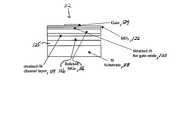
- FIG. 1Ais a cross section of a block diagram of a strained Si surface channel device 100 , in which a thin strained Si layer 102 is grown atop a relaxed SiGe virtual substrate.
- the SiGe virtual substratecan be relaxed SiGe 104 on a SiGe graded buffer 105 (as shown in FIG. 1 a ), relaxed SiGe directly on a Si substrate 106 , or relaxed SiGe on an insulator such as SiO 2 .
- the devicealso includes a SiO 2 layer 108 and gate material 110 .
- FIG. 1Bis a cross section of a block diagram of a strained Si buried channel device 112 , in which a SiGe layer 116 and a second strained Si layer 120 (used for gate oxidation) cap the strained Si channel layer 114 .
- the structurealso includes a graded SiGe buffer layer 125 and a second relaxed SiGe layer 126 .
- a gate oxide 122is grown or deposited and the gate material 124 is deposited to form the (MOS) structure.
- FIGS. 1A and 1Bthe invention is applicable to any heterostructure device fabricated on a relaxed SiGe platform.
- the heterostructure strained channelcould be Ge or SiGe of a different Ge content from that of the underlying SiGe virtual substrate.
- the following descriptionwill focus on the applicability of the invention to the strained Si device variants illustrated in FIGS. 1A and 1B.
- the SiGeIn order to form the MOS gate of the heterostructure device, the SiGe would ideally be oxidized directly in the buried channel device, and the strained Si would be oxidized directly in the surface channel device. Unfortunately, there are problems due to the nature of the Si/SiGe heterostructures in both cases that render the direct oxidation process unsatisfactory.
- the buried channel caseappears to be a better situation at first, since the Si layer thickness is buried.
- direct oxidation of SiGecreates a very high interface state density at the oxide/SiGe interface, leading to poor device performance.
- a known solution in the fieldis to create a thin Si layer at the surface of the buried channel structure. In this structure, the surface layer is carefully oxidized to nearly consume the entire top Si layer. However, a thin layer of un-oxidized Si is left so that the interface to the oxide is the superior SiO 2 /Si interface rather than the problematic oxide/SiGe interface.
- the structurenow has the same limits as the structure described above, i.e., the sacrificial Si layer will be slowly etched away during Si processing, possibly leading to exposure of the SiGe and degradation of the electrical properties of the interface as described.
- a method of fabricating a semiconductor deviceincluding providing a semiconductor heterostructure, the heterostructure having a relaxed Si 1-x Ge x layer on a substrate, a strained channel layer on the relaxed Si 1-x Ge x layer, and a Si 1-y Ge y layer; removing the Si 1-y Ge y layer; and providing a dielectric layer.
- the dielectric layerincludes a gate dielectric of a MISFET.
- the heterostructureincludes a SiGe spacer layer and a Si layer.
- FIGS. 1A and 1Bare cross sections of block diagrams of strained Si surface and buried channel devices, respectively;
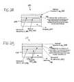
- FIGS. 2A and 2Bare cross sections of block diagrams of starting heterostructures for surface channel and buried channel strained MOS, respectively, in accordance with the invention.
- FIGS. 3 A- 3 Dare block diagrams showing the process sequence for a strained surface channel MOS device
- FIGS. 4 A- 4 Dare block diagrams showing the process sequence utilizing the gate structure for a buried channel device
- FIG. 5is a graph of oxidation rates, under a wet oxidation ambient at 700° C., of SiGe alloys, with Ge contents of 0.28 and 0.36, compared to the oxidation rate of bulk silicon;
- FIG. 6is a graph showing the oxide thickness of both a Si 0.7 Ge 0.3 alloy and a Si/Si 0.7 Ge 0.3 heterostructure
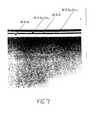
- FIG. 7is a cross-sectional transmission electron micrograph (XTEM) of the Si/Si 0.7 Ge 0.3 heterostructure
- FIG. 8is a XTEM image of the identical Si/Si 0.7 Ge 0.3 heterostructure after wet oxidation followed by oxide removal via a wet etch;
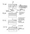
- FIG. 9is a structure for a buried channel MOSFET using relaxed SiGe and strained Si in accordance with the invention.
- FIG. 10is a graph showing a plot of the middle SiGe layer thickness (h2) and the resulting misfit dislocation spacing.
- a solution for the buried channel and surface channel structuresis to actually deposit another SiGe layer after the desired device structure (which, in the buried channel heterostructure, includes the sacrificial Si layer for oxidation).
- the structuresare shown in FIGS. 2A and 2B.
- FIG. 2Ais a cross section of a block diagram of a starting heterostructure 200 for surface channel strained MOS in accordance with the invention.
- the structure 200includes a Si substrate 202 , a SiGe graded buffer 204 , a relaxed SiGe layer 206 , and a strained-Si channel layer 208 .
- FIG. 2Bis a cross section of a block diagram of a starting heterostructure 214 for buried channel strained Si MOS.
- the structure 214includes a Si substrate 216 , a SiGe graded buffer 218 , relaxed SiGe layers 220 and 230 , a first strained-Si channel layer 222 and a second strained-Si layer 224 for the gate oxide.
- SiGe capping layer 210 , 226are identical to those depicted in FIGS. 1A and 1B before the gate stack formation, except for the addition of a SiGe capping layer 210 , 226 and an optional Si capping layer 212 , 228 . Since the SiGe layer 210 , 226 is closely lattice-matched to the relaxed SiGe layer below the device layers, there is essentially no limit on the thickness of the SiGe layer. This SiGe layer thickness can be tuned to the thickness of material removed before gate oxidation, so that the strained Si layer is exposed just before oxidation. Alternatively, the SiGe can be thicker than the removal thickness and then can be selectively removed.
- SiGecan be selectively removed with respect to Si using a variety of conventional Si-based processes. Therefore, cleaning and oxidation steps can be performed during the Si device and circuit fabrication process with little worry of consuming the precious strained Si and/or the sacrificial strained Si. One only needs to create a SiGe thick enough such that it is not totally consumed before the critical gate oxidation step.
- An additional optioncan be to place yet another Si layer 212 , 228 on top of the additional SiGe layer 210 , 226 .
- the idea of SiGe on the surface, instead of Si,is a factor for concern.
- another Si layercan be deposited on top of the additional SiGe layer described above.
- This phenomenonoccurs since the Si layers are tensile, and therefore dislocations introduced into the top optional Si layer have a Burgers vector that will not allow them to glide favorably in the compressive layer below.
- the dislocations in the top optional Si layer(if the Si layer critical thickness is exceeded) will not penetrate into the layers beneath it, and therefore as much Si can be deposited as desired.
- this optional Si capping layerneed not be strained at all in this case and can serve as a protective sacrificial layer even if it is fully relaxed.
- FIGS. 3 A- 3 Dare block diagrams showing the process sequence for a strained surface channel MOS device utilizing the gate structure described above (the process is shown for a structure without an optional strained surface layer).
- FIG. 3Ashows the initial Si/SiGe heterostructure 200 shown in FIG. 2A.
- FIG. 3Bshows the structure after the completion of the initial steps of a Si VLSI process, which could include wet chemical cleans and oxidation steps.
- the protective SiGe capping layer 210has been reduced in thickness, as a portion of the layer has been consumed during processing.
- the remainder of the protective SiGe capping layer 210is selectively removed, leaving the underlying Si layer 208 intact and exposed.
- a sacrificial oxidation step and oxide stripcan also be performed at this point to improve the quality of the exposed Si surface.
- FIG. 3Cshows the resulting structure after gate oxidation to form a gate oxide 300 , a structure in which the minimum possible amount of Si was consumed prior to the gate oxidation step.
- a gate oxide 300a structure in which the minimum possible amount of Si was consumed prior to the gate oxidation step.
- an alternate gate dielectriccould be deposited on the exposed Si surface.
- a pristine Si surfaceis just as important for a high quality interface with many deposited gate dielectrics as it is for a thermally grown SiO 2 gate dielectric.
- FIGS. 4 A- 4 Dare block diagrams showing the process sequence utilizing the gate structure for a buried channel device (the process is shown for a structure without an optional strained surface layer) using the initial Si/SiGe heterostructure 214 shown in FIG. 2B.
- the process stepsare identical to those of FIGS. 3 A- 3 D, but in the final heterostructure, the Si channel layer 222 is separated from the gate dielectric 400 by a SiGe spacer layer 220 , thus forming a buried channel.
- Using selective processes to etch down to the buried Si channel or the top Si layercan use the starting heterostructure 214 in FIG. 4A to form a surface channel device.
- Such a processcan result in enhancement mode and depletion mode devices that can in turn be used to create E/D logic circuits as well as a plethora of analog circuits.
- an exemplary sequence of stepsis: 1. Pre-gate-oxidation cleaning steps and oxidation; 2. Selective etch or oxidation to remove residual protective SiGe layer; 3. Sacrificial oxide formation on Si; 4. Sacrificial oxide strip; 5. Gate oxidation.
- steps 3 and 4can be optional, depending on whether there may be a small amount of Ge left on the surface after the selective removal of the SiGe protection layer.
- the SiGe/Si interfacewill not be infinitely abrupt, and therefore it is possible to have a small amount of Ge in the optimally pure Si layer.
- a sacrificial oxide stepcan be employed to remove an additional small amount of the Si layer to ensure that pure Si is oxidized in the gate oxidation step, ensuring high quality gate oxide.
- the second stepcan be accomplished in a variety of ways.
- One convenient processis a wet oxidation step, preferably at 750° C. or below. Under wet oxidation at these temperatures, SiGe is oxidized at rates that can be 100 times greater than rates oxidizing Si under the same conditions.
- SiGeis oxidized at rates that can be 100 times greater than rates oxidizing Si under the same conditions.
- a wet oxidation steppreferably at 750° C. or below.
- SiGeis oxidized at rates that can be 100 times greater than rates oxidizing Si under the same conditions.
- oxidized SiGecan be stripped to expose the Si.
- the low temperatureis not only important for the selectivity in the oxidation process, but also the low temperature is important to minimize or prevent the snow-plowing of Ge in front of the oxidation front, a known problem in the direct oxidation of SiGe.
- FIG. 5is a graph of oxidation rates, under a wet oxidation ambient at 700° C., of SiGe alloys, with Ge contents of 0.28 and 0.36, compared to the oxidation rate of bulk silicon. It is evident from the graph that, under such conditions, the oxidation rate of SiGe increases as the Ge content of the film increases.
- FIG. 6is a similar graph, showing the oxide thickness of both a Si 0.7 Ge 0.3 alloy and a Si/Si 0.7 Ge 0.3 heterostructure. Again, the oxidation conditions were 700° C. in a wet ambient; however, FIG. 6 depicts very short oxidation durations compared to FIG. 5.
- the Si/Si 0.7 Ge 0.3 heterostructureconsists of a 50 ⁇ strained Si buried layer, followed by a 30 ⁇ Si 0.7 Ge 0.3 , a 20 ⁇ strained Si layer and finally a 50 ⁇ Si 0.7 Ge 0.3 capping layer.
- FIG. 7A cross-sectional transmission electron micrograph (XTEM) of the Si/Si 0.7 Ge 0.3 heterostructure is shown in FIG. 7. It should be noted from FIG. 6 that the presence of strained Si layers in the heterostructure results in a dramatic retardation in the oxidation rate when compared to the oxidation rate of the uniform Si 0.7 Ge 0.3 . This retardation of the oxidation rate forms the basis of the selective removal of SiGe alloys over strained Si epitaxial layers.
- FIG. 8is a XTEM image of the identical Si/Si 0.7 Ge 0.3 heterostructure after wet oxidation at 700° C. for 2 minutes followed by oxide removal via a wet etch. It is apparent that the thin strained Si layer is unaffected by the selective oxidation and remains fully intact. Based on the data shown in FIG. 5, an oxidation duration of 2 minutes far exceeds that required to fully oxidize the 50 ⁇ Si 0.7 Ge 0.3 capping layer of the heterostructure.
- the very thin dark bandwhich is apparent on the surface of the strained Si layer, is a snow-plowed high Ge content layer that occurs during oxidation.
- Such a layermay be removed using a simple chemical clean or a sacrificial oxidation step, either or both of which typically occur prior to the formation of the gate oxide.
- the protective SiGe capping layercan be removed via selective dry or wet chemical etching techniques. For example, at high pressures (>200 mT) and low powers, CF 4 dry etch chemistries will etch relaxed SiGe films with high selectivity to Si. Mixtures of hydrofluoric acid (HF), hydrogen peroxide (H 2 O 2 ), and acetic acid (CH 3 COOH) will also selectively etch relaxed SiGe layers over Si at selectivities of 300:1 or more. Other potential selective wet chemical mixtures include HF, water (H 2 O), and either H 2 O 2 or nitric acid (HNO 3 ).
- HFhydrofluoric acid
- H 2 O 2hydrogen peroxide
- CH 3 COOHacetic acid
- the stability of the entire structurecan be improved by increasing the Ge concentration in the intermediate SiGe layer, and also the top SiGe layer if desired.
- energetic calculationsare used to reveal a guide to creating semiconductor layer structures that increase stability with respect to misfit dislocation introduction.
- the critical thickness for a buried channel MOSFET using relaxed SiGe and strained Sihas been determined using the energy-balance formulation.
- the structure consideredis the one shown in FIG. 9.
- the structure 900includes a 30% SiGe virtual substrate 902 topped by a 80 ⁇ strained Si layer 904 , a SiGe layer with Ge concentration ⁇ 2 and thickness h2 906 , and an additional 30 ⁇ of strained Si 908 . Additional stability would result from the addition of an additional SiGe cap layer as described previously.
- the example of FIG. 9considers only the increased stability created by increasing the Ge concentration ( ⁇ 2) or thickness (h2) of the SiGe intermediate layer. Additionally, since the SiGe cap layer is removed during processing, the stability of the heterostructure with the SiGe cap removed is or primary importance.
- the energy for a dislocation array (per unit area) inserted at the base of the compositeis:
- h Tis the total thickness of the composite (h 1 +h 2+h 3 )
- ⁇is the angle between the dislocation line and the Burgers vector b
- vis the Poisson ratio
- Dis the average shear modulus for a dislocation lying at the interface between the virtual substrate and the composite structure.
- h T⁇ i n ⁇ ⁇ h i .
- FIG. 10is a graph showing a plot of the middle SiGe layer thickness (h2) and the resulting misfit dislocation spacing.
- the sharp upturn on the plotsrepresents the critical thickness h2 of the middle SiGe layer when the entire composite structure destabilizes and introduces dislocations at the channel/virtual buffer interface.
- the different curvesare for the different compositions in the second layer h2.
- Very small increases in Geresult in a large jump in stability of the device layers. This suggests that it is possible to stabilize the layer significantly but not have the band structure altered that much. Adding an extra 5-10% Ge into the h2 layer increases the stability drastically.
- FIG. 10indicates that over 100 ⁇ of 30% Ge is required to provide the stability of a 20 ⁇ layer of 45% Ge content.
- Sacrificial SiGe capping layersprovide an innovative method for the protection of thin strained device layers during processing. Such layers shield these critically important strained channel layers from process steps, such as wet chemical cleans and oxidations, which consume surface material. Before the growth or deposition of the gate dielectric, these protective SiGe layers can be selectively removed by standard processes such as oxidation or wet etching, revealing the intact strained device layer. Also presented is a guideline for engineering strained layer stacks such that relaxation via misfit dislocation is prevented. Compressively strained intermediate layers increase the stability of tensile channel layers, and also serve as a barrier for misfit dislocation introduction into the underlying layers.
Landscapes
- Engineering & Computer Science (AREA)
- Physics & Mathematics (AREA)
- Condensed Matter Physics & Semiconductors (AREA)
- General Physics & Mathematics (AREA)
- Manufacturing & Machinery (AREA)
- Computer Hardware Design (AREA)
- Microelectronics & Electronic Packaging (AREA)
- Power Engineering (AREA)
- Chemical & Material Sciences (AREA)
- Materials Engineering (AREA)
- Insulated Gate Type Field-Effect Transistor (AREA)
- Thin Film Transistor (AREA)
Abstract
Description
- This application claims priority from provisional application Ser. No. 60/223,595 filed Aug. 7, 2000.[0001]
- The invention relates to gate technology for strained surface channel and strained buried channel MOSFET devices.[0002]
- The advent of high quality relaxed SiGe layers on Si has resulted in the demonstration of field effect transistors (FETs) with carrier channels enhanced via strain. The strain can be incorporated in the channel due to the lattice mismatch between the channel and the relaxed SiGe created by a change in the Ge concentration between the channel layer and the relaxed SiGe layer. For example, a Ge concentration of 20% Ge in the relaxed buffer is high enough such that a thin strained Si layer can exhibit electron mobilities as high as 1000-2900 cm[0003]2/V-sec. Also, if the Ge concentration in the channel is greater than the concentration in the buffer, hole channel mobilities can be enhanced. For example, a relaxed buffer concentration of 60-70% Ge can compressively strain a Ge channel layer, creating potentially extremely high hole mobilities.
- Although the exact physics of carrier scattering are not known inside short-channel FETs, one thing is clear: these enhanced mobilities translate into increased device performance, even at very short gate lengths. In addition to higher speed and a different power-delay product, the use of strained channels allows for the incorporation of new FET structures into Si-based circuits. Thus, it is anticipated that the high performance, new flexibility in device design, and economics of using a Si-based platform will lead to a plethora of new circuits and products.[0004]
- With regards to these new circuits and products, the devices based on metal-insulator-semiconductor (MIS) or metal-oxide-semiconductor (MOS) gate technology are the most intriguing, since these devices can follow very closely the processes already used in Si VLSI manufacturing. Two main types of devices are of particular interest: the surface channel device and the buried channel device, examples of which are shown in FIGS. 1A and 1B.[0005]
- FIG. 1A is a cross section of a block diagram of a strained Si[0006]
surface channel device 100, in which a thinstrained Si layer 102 is grown atop a relaxed SiGe virtual substrate. The SiGe virtual substrate can be relaxed SiGe104 on a SiGe graded buffer105 (as shown in FIG. 1a), relaxed SiGe directly on aSi substrate 106, or relaxed SiGe on an insulator such as SiO2. The device also includes a SiO2layer108 and gate material110. - FIG. 1B is a cross section of a block diagram of a strained Si buried[0007]
channel device 112, in which a SiGe layer116 and a second strained Si layer120 (used for gate oxidation) cap the strainedSi channel layer 114. The structure also includes a gradedSiGe buffer layer 125 and a secondrelaxed SiGe layer 126. In both device configurations, a gate oxide122 is grown or deposited and thegate material 124 is deposited to form the (MOS) structure. Although only devices with strained Si channels are shown in FIGS. 1A and 1B, the invention is applicable to any heterostructure device fabricated on a relaxed SiGe platform. For example, the heterostructure strained channel could be Ge or SiGe of a different Ge content from that of the underlying SiGe virtual substrate. However, the following description will focus on the applicability of the invention to the strained Si device variants illustrated in FIGS. 1A and 1B. - In order to form the MOS gate of the heterostructure device, the SiGe would ideally be oxidized directly in the buried channel device, and the strained Si would be oxidized directly in the surface channel device. Unfortunately, there are problems due to the nature of the Si/SiGe heterostructures in both cases that render the direct oxidation process unsatisfactory.[0008]
- First consider the surface channel device. Since Si is being oxidized, the interface state density at the resulting SiO[0009]2/Si interface is low, and an electrically high quality interface results. However, all oxidation and cleaning processes during the device and circuit fabrication consume the Si material. In conventional Si processing, there is generally little worry about Si consumption since so little material is consumed compared to any limiting vertical dimension early in the fabrication process. However, in the case of the strained surface channel FET described here, the top strained Si layer is typically less than 300 Å thick, and thus too much Si consumption during cleaning and oxidation steps will eliminate the high mobility channel.
- One obvious solution is to simply deposit extra Si at the surface, planning for the removal of the Si that occurs during processing. However, the channel strain, which gives the channel its higher carrier mobility, limits the Si layer thickness. At a great enough thickness, the Si layer will begin to relax, introducing misfit dislocations at the Si/SiGe interface. This process of dislocation introduction has two deleterious effects on device performance. First, the strain in the Si is partially or completely relieved, potentially decreasing the carrier mobility enhancements. Second, dislocations can scatter carriers, decreasing carrier mobility. Dislocations can also affect device yield, reliability, and performance.[0010]
- The buried channel case appears to be a better situation at first, since the Si layer thickness is buried. However, in this case, direct oxidation of SiGe creates a very high interface state density at the oxide/SiGe interface, leading to poor device performance. A known solution in the field is to create a thin Si layer at the surface of the buried channel structure. In this structure, the surface layer is carefully oxidized to nearly consume the entire top Si layer. However, a thin layer of un-oxidized Si is left so that the interface to the oxide is the superior SiO[0011]2/Si interface rather than the problematic oxide/SiGe interface. Although this sacrificial surface Si layer solves the interface electronic property issue, the structure now has the same limits as the structure described above, i.e., the sacrificial Si layer will be slowly etched away during Si processing, possibly leading to exposure of the SiGe and degradation of the electrical properties of the interface as described.
- In accordance with the invention there is provided a method of fabricating a semiconductor device including providing a semiconductor heterostructure, the heterostructure having a relaxed Si[0012]1-xGexlayer on a substrate, a strained channel layer on the relaxed Si1-xGexlayer, and a Si1-yGeylayer; removing the Si1-yGeylayer; and providing a dielectric layer. The dielectric layer includes a gate dielectric of a MISFET. In alternative embodiments, the heterostructure includes a SiGe spacer layer and a Si layer.
- FIGS. 1A and 1B are cross sections of block diagrams of strained Si surface and buried channel devices, respectively;[0013]
- FIGS. 2A and 2B are cross sections of block diagrams of starting heterostructures for surface channel and buried channel strained MOS, respectively, in accordance with the invention;[0014]
- FIGS.[0015]3A-3D are block diagrams showing the process sequence for a strained surface channel MOS device;
- FIGS.[0016]4A-4D are block diagrams showing the process sequence utilizing the gate structure for a buried channel device;
- FIG. 5 is a graph of oxidation rates, under a wet oxidation ambient at 700° C., of SiGe alloys, with Ge contents of 0.28 and 0.36, compared to the oxidation rate of bulk silicon;[0017]
- FIG. 6 is a graph showing the oxide thickness of both a Si[0018]0.7Ge0.3alloy and a Si/Si0.7Ge0.3heterostructure;
- FIG. 7 is a cross-sectional transmission electron micrograph (XTEM) of the Si/Si[0019]0.7Ge0.3heterostructure;
- FIG. 8 is a XTEM image of the identical Si/Si[0020]0.7Ge0.3heterostructure after wet oxidation followed by oxide removal via a wet etch;
- FIG. 9 is a structure for a buried channel MOSFET using relaxed SiGe and strained Si in accordance with the invention; and[0021]
- FIG. 10 is a graph showing a plot of the middle SiGe layer thickness (h2) and the resulting misfit dislocation spacing.[0022]
- To eliminate the issue of losing valuable surface Si, an innovative step that has not been previously considered can be employed. In fact, any interest in this area is dominated by discussions of how to change the Si device and circuit process to conserve Si consumption. Although these are certainly possibilities, such constraints severely limit process flexibility, alter the process further from the conventional Si process, and most likely will increase the cost of the fabrication process.[0023]
- A solution for the buried channel and surface channel structures is to actually deposit another SiGe layer after the desired device structure (which, in the buried channel heterostructure, includes the sacrificial Si layer for oxidation). The structures are shown in FIGS. 2A and 2B.[0024]
- FIG. 2A is a cross section of a block diagram of a starting[0025]
heterostructure 200 for surface channel strained MOS in accordance with the invention. Thestructure 200 includes aSi substrate 202, a SiGe gradedbuffer 204, arelaxed SiGe layer 206, and a strained-Si channel layer 208. FIG. 2B is a cross section of a block diagram of a startingheterostructure 214 for buried channel strained Si MOS. Thestructure 214 includes aSi substrate 216, a SiGe gradedbuffer 218, relaxed SiGe layers220 and230, a first strained-Si channel layer 222 and a second strained-Si layer224 for the gate oxide. - These structures are identical to those depicted in FIGS. 1A and 1B before the gate stack formation, except for the addition of a[0026]
SiGe capping layer Si capping layer 212,228. Since theSiGe layer - An additional option can be to place yet another[0027]
Si layer 212,228 on top of theadditional SiGe layer - FIGS.[0028]3A-3D are block diagrams showing the process sequence for a strained surface channel MOS device utilizing the gate structure described above (the process is shown for a structure without an optional strained surface layer). FIG. 3A shows the initial Si/SiGe heterostructure200 shown in FIG. 2A. FIG. 3B shows the structure after the completion of the initial steps of a Si VLSI process, which could include wet chemical cleans and oxidation steps. Thus, in FIG. 3B, the protective
SiGe capping layer 210 has been reduced in thickness, as a portion of the layer has been consumed during processing. Next, the remainder of the protectiveSiGe capping layer 210 is selectively removed, leaving theunderlying Si layer 208 intact and exposed. A sacrificial oxidation step and oxide strip can also be performed at this point to improve the quality of the exposed Si surface. - The resulting structure is shown in FIG. 3C. FIG. 3D shows the final device structure after gate oxidation to form a[0029]
gate oxide 300, a structure in which the minimum possible amount of Si was consumed prior to the gate oxidation step. Alternatively, at this point an alternate gate dielectric could be deposited on the exposed Si surface. A pristine Si surface is just as important for a high quality interface with many deposited gate dielectrics as it is for a thermally grown SiO2gate dielectric. - FIGS.[0030]4A-4D are block diagrams showing the process sequence utilizing the gate structure for a buried channel device (the process is shown for a structure without an optional strained surface layer) using the initial Si/SiGe heterostructure214 shown in FIG. 2B. The process steps are identical to those of FIGS.3A-3D, but in the final heterostructure, the
Si channel layer 222 is separated from thegate dielectric 400 by aSiGe spacer layer 220, thus forming a buried channel. Using selective processes to etch down to the buried Si channel or the top Si layer can use the startingheterostructure 214 in FIG. 4A to form a surface channel device. Such a process can result in enhancement mode and depletion mode devices that can in turn be used to create E/D logic circuits as well as a plethora of analog circuits. - In both sequences, an exemplary sequence of steps is: 1. Pre-gate-oxidation cleaning steps and oxidation; 2. Selective etch or oxidation to remove residual protective SiGe layer; 3. Sacrificial oxide formation on Si; 4. Sacrificial oxide strip; 5. Gate oxidation.[0031]
- It will be appreciated that steps[0032]3 and4 can be optional, depending on whether there may be a small amount of Ge left on the surface after the selective removal of the SiGe protection layer. When the original heterostructure is grown, the SiGe/Si interface will not be infinitely abrupt, and therefore it is possible to have a small amount of Ge in the optimally pure Si layer. A sacrificial oxide step can be employed to remove an additional small amount of the Si layer to ensure that pure Si is oxidized in the gate oxidation step, ensuring high quality gate oxide.
- The second step, the selective removal of the residual SiGe protective material, can be accomplished in a variety of ways. One convenient process is a wet oxidation step, preferably at 750° C. or below. Under wet oxidation at these temperatures, SiGe is oxidized at rates that can be 100 times greater than rates oxidizing Si under the same conditions. Thus, in order to expose the Si for gate oxidation, one can simply do a wet oxidation of the SiGe layer and selectively stop at the Si layer. The oxidized SiGe can be stripped to expose the Si. It is important to note here that the low temperature is not only important for the selectivity in the oxidation process, but also the low temperature is important to minimize or prevent the snow-plowing of Ge in front of the oxidation front, a known problem in the direct oxidation of SiGe.[0033]
- FIG. 5 is a graph of oxidation rates, under a wet oxidation ambient at 700° C., of SiGe alloys, with Ge contents of 0.28 and 0.36, compared to the oxidation rate of bulk silicon. It is evident from the graph that, under such conditions, the oxidation rate of SiGe increases as the Ge content of the film increases.[0034]
- FIG. 6 is a similar graph, showing the oxide thickness of both a Si[0035]0.7Ge0.3alloy and a Si/Si0.7Ge0.3heterostructure. Again, the oxidation conditions were 700° C. in a wet ambient; however, FIG. 6 depicts very short oxidation durations compared to FIG. 5. The Si/Si0.7Ge0.3heterostructure consists of a 50 Å strained Si buried layer, followed by a 30 Å Si0.7Ge0.3, a 20 Å strained Si layer and finally a 50 Å Si0.7Ge0.3capping layer.
- A cross-sectional transmission electron micrograph (XTEM) of the Si/Si[0036]0.7Ge0.3heterostructure is shown in FIG. 7. It should be noted from FIG. 6 that the presence of strained Si layers in the heterostructure results in a dramatic retardation in the oxidation rate when compared to the oxidation rate of the uniform Si0.7Ge0.3. This retardation of the oxidation rate forms the basis of the selective removal of SiGe alloys over strained Si epitaxial layers.
- FIG. 8 is a XTEM image of the identical Si/Si[0037]0.7Ge0.3heterostructure after wet oxidation at 700° C. for 2 minutes followed by oxide removal via a wet etch. It is apparent that the thin strained Si layer is unaffected by the selective oxidation and remains fully intact. Based on the data shown in FIG. 5, an oxidation duration of 2 minutes far exceeds that required to fully oxidize the 50 Å Si0.7Ge0.3capping layer of the heterostructure. The very thin dark band, which is apparent on the surface of the strained Si layer, is a snow-plowed high Ge content layer that occurs during oxidation. Such a layer may be removed using a simple chemical clean or a sacrificial oxidation step, either or both of which typically occur prior to the formation of the gate oxide.
- Alternatively, the protective SiGe capping layer can be removed via selective dry or wet chemical etching techniques. For example, at high pressures (>200 mT) and low powers, CF[0038]4dry etch chemistries will etch relaxed SiGe films with high selectivity to Si. Mixtures of hydrofluoric acid (HF), hydrogen peroxide (H2O2), and acetic acid (CH3COOH) will also selectively etch relaxed SiGe layers over Si at selectivities of 300:1 or more. Other potential selective wet chemical mixtures include HF, water (H2O), and either H2O2or nitric acid (HNO3).
- Additionally, the stability of the entire structure can be improved by increasing the Ge concentration in the intermediate SiGe layer, and also the top SiGe layer if desired. Below, energetic calculations are used to reveal a guide to creating semiconductor layer structures that increase stability with respect to misfit dislocation introduction.[0039]
- The critical thickness for a buried channel MOSFET using relaxed SiGe and strained Si has been determined using the energy-balance formulation. The structure considered is the one shown in FIG. 9. The[0040]
structure 900 includes a 30% SiGevirtual substrate 902 topped by a 80 Å strained Si layer904, a SiGe layer with Ge concentration ×2 andthickness h2 906, and an additional 30 Å of strained Si908. Additional stability would result from the addition of an additional SiGe cap layer as described previously. To simplify, the example of FIG. 9 considers only the increased stability created by increasing the Ge concentration (×2) or thickness (h2) of the SiGe intermediate layer. Additionally, since the SiGe cap layer is removed during processing, the stability of the heterostructure with the SiGe cap removed is or primary importance. - In device processing, one must consider the critical thickness of the entire structure with respect to the relaxed virtual substrate. Individual layers that exceed the individual critical thicknesses are not explicitly ruled out, so one practicing the art would have to verify that none of the layers that are introduced into the desired structure exceed the individual layer critical thicknesses. In other words, in the following calculation it is assumed that each layer in the structure is below its critical thickness with respect to the relaxed buffer.[0041]
- One key to the formulation is to realize that this calculation should be done with respect to the plastic deformation of the layer composite, δ. Then, the dislocation array energy is the same expression regardless of the layer structure. The elastic energy in the individual layers is changed because of δ. In tensile layers, the strain is lowered by δ. In compressive layers, the energy is raised by δ.[0042]
- Thus, the energy for a dislocation array (per unit area) inserted at the base of the composite is:[0043]
- Eδ=2δD(1−vcos α)[In(hT/b)+1]
- where h[0044]Tis the total thickness of the composite (h1+h2+h3), α is the angle between the dislocation line and the Burgers vector b, v is the Poisson ratio, and D is the average shear modulus for a dislocation lying at the interface between the virtual substrate and the composite structure.
- where Y is the Young's modulus. Thus, the total energy of the system is:[0046]
- ET=Eδ+Eε.
- The amount of plastic deformation and resulting misfit dislocation spacing S was calculated for the structure depicted in FIG. 9 as follows:[0050]
- Lower strained Si layer thickness h1=80 Å[0051]
- Upper strained Si layer thickness h3=30 Å[0052]
- Middle SiGe layer thickness h2 variable[0053]
- Middle SiGe layer Ge concentration x2 variable Virtual substrate Ge concentration: 30%[0054]
- FIG. 10 is a graph showing a plot of the middle SiGe layer thickness (h2) and the resulting misfit dislocation spacing. The sharp upturn on the plots represents the critical thickness h2 of the middle SiGe layer when the entire composite structure destabilizes and introduces dislocations at the channel/virtual buffer interface. The different curves are for the different compositions in the second layer h2. Very small increases in Ge result in a large jump in stability of the device layers. This suggests that it is possible to stabilize the layer significantly but not have the band structure altered that much. Adding an extra 5-10% Ge into the h2 layer increases the stability drastically. For example, FIG. 10 indicates that over 100 Å of 30% Ge is required to provide the stability of a 20 Å layer of 45% Ge content.[0055]
- Increasing h2 even when the h2 layer is lattice-matched to the virtual buffer increases the stability of the multilayer structure. In the equations above, the effect can be seen to be much weaker than when a compressive strain in h2 is created. When f2 is zero due to lattice matching to the virtual buffer, the increased stability with increasing h2 comes from the fact that h[0056]τ is increasing and therefore decreasing δ (and increasing S).
- It will be appreciated that all the calculations are equilibrium calculations, and as usual, one might suspect that these numbers are somewhat conservative, although also consider that the layers possess many threading dislocations that can bend over at the critical thickness, so there are plenty of sources for misfit dislocation generation.[0057]
- Sacrificial SiGe capping layers provide an innovative method for the protection of thin strained device layers during processing. Such layers shield these critically important strained channel layers from process steps, such as wet chemical cleans and oxidations, which consume surface material. Before the growth or deposition of the gate dielectric, these protective SiGe layers can be selectively removed by standard processes such as oxidation or wet etching, revealing the intact strained device layer. Also presented is a guideline for engineering strained layer stacks such that relaxation via misfit dislocation is prevented. Compressively strained intermediate layers increase the stability of tensile channel layers, and also serve as a barrier for misfit dislocation introduction into the underlying layers.[0058]
- Although the present invention has been shown and described with respect to several preferred embodiments thereof, various changes, omissions and additions to the form and detail thereof, may be made therein, without departing from the spirit and scope of the invention.[0059]


Claims (39)
1. A method of fabricating a semiconductor device comprising:
providing a semiconductor heterostructure, said heterostructure comprising a relaxed Si1-xGexlayer on a substrate, a strained channel layer on said relaxed Si1-xGexlayer, and a Si1-yGeylayer;
removing said Si1-yGeylayer; and
providing a dielectric layer.
2. The method ofclaim 1 , wherein said Si1-yGeylayer is removed by a selective technique.
3. The method ofclaim 2 , wherein said selective technique is wet oxidation below 750° C.
4. The method ofclaim 2 , wherein said selective technique is a wet or dry chemical etch.
5. The method ofclaim 1 , wherein said dielectric layer comprises a gate dielectric of a MISFET.
6. The method ofclaim 5 , wherein the gate dielectric comprises an oxide.
7. The method ofclaim 5 , wherein the gate dielectric is deposited.
8. The method ofclaim 5 , wherein the MISFET comprises a surface channel device.
9. The method ofclaim 5 , wherein the MISFET comprises a buried channel device.
10. The method ofclaim 1 , wherein the strained channel layer comprises Si.
11. The method ofclaim 1 , wherein x is approximately equal to y.
12. The method ofclaim 11 further comprising a sacrificial Si layer on said sacrificial Si1-yGeylayer.
13. The method ofclaim 1 , wherein y>x.
14. The method ofclaim 13 further comprising a sacrificial Si layer on said sacrificial Si1-yGeylayer.
15. The method ofclaim 14 , wherein the thickness of the sacrificial Si layer is greater than the critical thickness.
16. The method ofclaim 1 , wherein the substrate comprises Si.
17. The method ofclaim 1 , wherein the substrate comprises Si with a layer of SiO2.
18. The method ofclaim 1 , wherein the substrate comprises a SiGe graded buffer layer on Si.
19. The method ofclaim 1 , wherein the semiconductor device comprises a MISFET.
20. A method of fabricating a semiconductor device comprising:
providing a semiconductor heterostructure, said heterostructure comprising a relaxed Si1-xGexlayer on a substrate, a strained channel layer on said relaxed Si1-xGexlayer, and a Si1-yGeylayer;
removing said Si1-yGeylayer to expose said strained channel layer;
removing a portion of said strained channel layer to eliminate any residual Ge; and
providing a dielectric layer.
21. A method of fabricating a semiconductor device comprising:
providing a semiconductor heterostructure, said heterostructure comprising a relaxed Si1-xGexlayer on a substrate, a strained channel layer on said relaxed Si1-xGexlayer, a Si1-yGeyspacer layer, and a Si1-wGewlayer;
removing said Si1-wGewlayer; and
providing a dielectric layer.
22. The method ofclaim 21 , wherein said dielectric layer comprises the gate dielectric of a MISFET.
23. The method ofclaim 22 , wherein the gate dielectric comprises an oxide.
24. The method ofclaim 22 , wherein the gate dielectric is deposited.
25. The method ofclaim 22 , wherein the MISFET comprises a buried channel device.
26. The method ofclaim 21 , wherein the strained channel comprises Si.
27. The method ofclaim 21 , wherein w is approximately equal to y.
28. The method ofclaim 27 further comprising a sacrificial Si layer on said sacrificial Si1-wGewlayer.
29. The method ofclaim 21 , wherein w>y.
30. The method ofclaim 29 further comprising a sacrificial Si layer on said sacrificial Si1-wGewlayer.
31. The method ofclaim 30 , wherein the thickness of the sacrificial Si layer is greater than the critical thickness.
32. The method ofclaim 21 , wherein the substrate comprises Si.
33. The method ofclaim 21 , wherein the substrate comprises Si with a layer of SiO2.
34. The method ofclaim 21 , wherein the substrate comprises a SiGe graded buffer layer on Si.
35. The method ofclaim 21 , wherein the semiconductor device comprises a MISFET.
36. A method of fabricating a semiconductor device comprising:
providing a semiconductor heterostructure, said heterostructure comprising a relaxed Si1-xGexlayer on a substrate, a strained channel layer on said relaxed Si1-xGexlayer, a Si1-yGeyspacer layer, a Si layer, and a Si1-wGewlayer;
removing said Si1-wGewlayer to expose said Si layer; and
providing a dielectric layer.
37. A method of fabricating a semiconductor device comprising:
providing a semiconductor heterostructure, said heterostructure comprising a relaxed Si1-xGexlayer on a substrate, a strained channel layer on said relaxed Si1-xGexlayer, a Si1-yGeyspacer layer, a Si layer, and a Si1-wGewlayer;
removing said Si1-wGewlayer to expose said Si layer; and
oxidizing said Si layer.
38. The method ofclaim 37 , wherein the semiconductor device comprises a MOSFET.
39. The method ofclaim 37 , wherein the semiconductor device comprises a buried channel MOSFET.
Priority Applications (4)
| Application Number | Priority Date | Filing Date | Title |
|---|---|---|---|
| US09/923,207US6583015B2 (en) | 2000-08-07 | 2001-08-06 | Gate technology for strained surface channel and strained buried channel MOSFET devices |
| US10/421,154US6846715B2 (en) | 2000-08-07 | 2003-04-23 | Gate technology for strained surface channel and strained buried channel MOSFET devices |
| US11/013,838US7217668B2 (en) | 2000-08-07 | 2004-12-16 | Gate technology for strained surface channel and strained buried channel MOSFET devices |
| US11/520,175US20070082470A1 (en) | 2000-08-07 | 2006-09-13 | Gate technology for strained surface channel and strained buried channel MOSFET devices |
Applications Claiming Priority (2)
| Application Number | Priority Date | Filing Date | Title |
|---|---|---|---|
| US22359500P | 2000-08-07 | 2000-08-07 | |
| US09/923,207US6583015B2 (en) | 2000-08-07 | 2001-08-06 | Gate technology for strained surface channel and strained buried channel MOSFET devices |
Related Child Applications (1)
| Application Number | Title | Priority Date | Filing Date |
|---|---|---|---|
| US10/421,154ContinuationUS6846715B2 (en) | 2000-08-07 | 2003-04-23 | Gate technology for strained surface channel and strained buried channel MOSFET devices |
Publications (2)
| Publication Number | Publication Date |
|---|---|
| US20020068393A1true US20020068393A1 (en) | 2002-06-06 |
| US6583015B2 US6583015B2 (en) | 2003-06-24 |
Family
ID=22837179
Family Applications (5)
| Application Number | Title | Priority Date | Filing Date |
|---|---|---|---|
| US09/923,207Expired - LifetimeUS6583015B2 (en) | 2000-08-07 | 2001-08-06 | Gate technology for strained surface channel and strained buried channel MOSFET devices |
| US09/922,822AbandonedUS20020104993A1 (en) | 2000-08-07 | 2001-08-06 | Gate technology for strained surface channel and strained buried channel MOSFET devices |
| US10/421,154Expired - LifetimeUS6846715B2 (en) | 2000-08-07 | 2003-04-23 | Gate technology for strained surface channel and strained buried channel MOSFET devices |
| US11/013,838Expired - LifetimeUS7217668B2 (en) | 2000-08-07 | 2004-12-16 | Gate technology for strained surface channel and strained buried channel MOSFET devices |
| US11/520,175AbandonedUS20070082470A1 (en) | 2000-08-07 | 2006-09-13 | Gate technology for strained surface channel and strained buried channel MOSFET devices |
Family Applications After (4)
| Application Number | Title | Priority Date | Filing Date |
|---|---|---|---|
| US09/922,822AbandonedUS20020104993A1 (en) | 2000-08-07 | 2001-08-06 | Gate technology for strained surface channel and strained buried channel MOSFET devices |
| US10/421,154Expired - LifetimeUS6846715B2 (en) | 2000-08-07 | 2003-04-23 | Gate technology for strained surface channel and strained buried channel MOSFET devices |
| US11/013,838Expired - LifetimeUS7217668B2 (en) | 2000-08-07 | 2004-12-16 | Gate technology for strained surface channel and strained buried channel MOSFET devices |
| US11/520,175AbandonedUS20070082470A1 (en) | 2000-08-07 | 2006-09-13 | Gate technology for strained surface channel and strained buried channel MOSFET devices |
Country Status (5)
| Country | Link |
|---|---|
| US (5) | US6583015B2 (en) |
| EP (1) | EP1307917A2 (en) |
| JP (1) | JP2004519090A (en) |
| AU (1) | AU2001283138A1 (en) |
| WO (1) | WO2002013262A2 (en) |
Cited By (21)
| Publication number | Priority date | Publication date | Assignee | Title |
|---|---|---|---|---|
| US20020123167A1 (en)* | 2001-03-02 | 2002-09-05 | Fitzgerald Eugene A. | Relaxed silicon germanium platform for high speed CMOS electronics and high speed analog circuits |
| US20030077867A1 (en)* | 2001-03-02 | 2003-04-24 | Fitzergald Eugene A. | Relaxed silicon germanium platform for high speed CMOS electronics and high speed analog circuits |
| US20030102498A1 (en)* | 2001-09-24 | 2003-06-05 | Glyn Braithwaite | RF circuits including transistors having strained material layers |
| US6593641B1 (en)* | 2001-03-02 | 2003-07-15 | Amberwave Systems Corporation | Relaxed silicon germanium platform for high speed CMOS electronics and high speed analog circuits |
| US20030168654A1 (en)* | 2000-08-16 | 2003-09-11 | Massachusetts Institute Of Technology | Process for producing semiconductor article using graded epitaxial growth |
| US6649480B2 (en) | 2000-12-04 | 2003-11-18 | Amberwave Systems Corporation | Method of fabricating CMOS inverter and integrated circuits utilizing strained silicon surface channel MOSFETs |
| US20030215990A1 (en)* | 2002-03-14 | 2003-11-20 | Eugene Fitzgerald | Methods for fabricating strained layers on semiconductor substrates |
| US6703688B1 (en) | 2001-03-02 | 2004-03-09 | Amberwave Systems Corporation | Relaxed silicon germanium platform for high speed CMOS electronics and high speed analog circuits |
| US6724008B2 (en) | 2001-03-02 | 2004-04-20 | Amberwave Systems Corporation | Relaxed silicon germanium platform for high speed CMOS electronics and high speed analog circuits |
| US20040092051A1 (en)* | 2002-10-30 | 2004-05-13 | Amberwave Systems Corporation | Methods for preserving strained semiconductor substrate layers during CMOS processing |
| US6803240B1 (en)* | 2003-09-03 | 2004-10-12 | International Business Machines Corporation | Method of measuring crystal defects in thin Si/SiGe bilayers |
| US20050054168A1 (en)* | 2001-09-21 | 2005-03-10 | Amberwave Systems Corporation | Semiconductor structures employing strained material layers with defined impurity gradients and methods for fabricating same |
| US6900103B2 (en)* | 2001-03-02 | 2005-05-31 | Amberwave Systems Corporation | Relaxed silicon germanium platform for high speed CMOS electronics and high speed analog circuits |
| US6924167B1 (en)* | 2002-08-15 | 2005-08-02 | Foveon, Inc. | Method of forming a bandgap tuned vertical color imager cell |
| US7122449B2 (en) | 2002-06-10 | 2006-10-17 | Amberwave Systems Corporation | Methods of fabricating semiconductor structures having epitaxially grown source and drain elements |
| US20060234455A1 (en)* | 2005-04-19 | 2006-10-19 | Chien-Hao Chen | Structures and methods for forming a locally strained transistor |
| US7217603B2 (en) | 2002-06-25 | 2007-05-15 | Amberwave Systems Corporation | Methods of forming reacted conductive gate electrodes |
| US20070173022A1 (en)* | 2006-01-20 | 2007-07-26 | Chih-Hao Wang | Defect-free SiGe source/drain formation by epitaxy-free process |
| US7504704B2 (en) | 2003-03-07 | 2009-03-17 | Amberwave Systems Corporation | Shallow trench isolation process |
| US7615829B2 (en) | 2002-06-07 | 2009-11-10 | Amberwave Systems Corporation | Elevated source and drain elements for strained-channel heterojuntion field-effect transistors |
| CN109950153A (en)* | 2019-03-08 | 2019-06-28 | 中国科学院微电子研究所 | Semiconductor structure and method of making the same |
Families Citing this family (86)
| Publication number | Priority date | Publication date | Assignee | Title |
|---|---|---|---|---|
| JP3535527B2 (en)* | 1997-06-24 | 2004-06-07 | マサチューセッツ インスティテュート オブ テクノロジー | Controlling threading dislocations in germanium-on-silicon using graded GeSi layer and planarization |
| US7227176B2 (en) | 1998-04-10 | 2007-06-05 | Massachusetts Institute Of Technology | Etch stop layer system |
| JP2003520444A (en) | 2000-01-20 | 2003-07-02 | アンバーウェーブ システムズ コーポレイション | Low threading dislocation density lattice-mismatched epilayer that does not require high-temperature growth |
| US6602613B1 (en) | 2000-01-20 | 2003-08-05 | Amberwave Systems Corporation | Heterointegration of materials using deposition and bonding |
| JP2004519090A (en)* | 2000-08-07 | 2004-06-24 | アンバーウェーブ システムズ コーポレイション | Gate technology for strained surface channel and strained buried channel MOSFET devices |
| US20020100942A1 (en)* | 2000-12-04 | 2002-08-01 | Fitzgerald Eugene A. | CMOS inverter and integrated circuits utilizing strained silicon surface channel MOSFETs |
| AU2002306436A1 (en)* | 2001-02-12 | 2002-10-15 | Asm America, Inc. | Improved process for deposition of semiconductor films |
| WO2002071488A1 (en)* | 2001-03-02 | 2002-09-12 | Amberwave Systems Corporation | Relaxed silicon germanium platform for high speed cmos electronics and high speed analog circuits |
| US6646322B2 (en) | 2001-03-02 | 2003-11-11 | Amberwave Systems Corporation | Relaxed silicon germanium platform for high speed CMOS electronics and high speed analog circuits |
| WO2002071493A2 (en)* | 2001-03-02 | 2002-09-12 | Amberwave Systems Corporation | Relaxed silicon germanium platform for high speed cmos electronics and high speed analog |
| WO2002082514A1 (en) | 2001-04-04 | 2002-10-17 | Massachusetts Institute Of Technology | A method for semiconductor device fabrication |
| AU2002322105A1 (en) | 2001-06-14 | 2003-01-02 | Amberware Systems Corporation | Method of selective removal of sige alloys |
| US7301180B2 (en) | 2001-06-18 | 2007-11-27 | Massachusetts Institute Of Technology | Structure and method for a high-speed semiconductor device having a Ge channel layer |
| WO2003001671A2 (en) | 2001-06-21 | 2003-01-03 | Amberwave Systems Corporation | Improved enhancement of p-type metal-oxide-semiconductor field-effect transistors |
| EP1415331A2 (en) | 2001-08-06 | 2004-05-06 | Massachusetts Institute Of Technology | Formation of planar strained layers |
| US6974735B2 (en) | 2001-08-09 | 2005-12-13 | Amberwave Systems Corporation | Dual layer Semiconductor Devices |
| US7138649B2 (en) | 2001-08-09 | 2006-11-21 | Amberwave Systems Corporation | Dual-channel CMOS transistors with differentially strained channels |
| JP3970011B2 (en)* | 2001-12-11 | 2007-09-05 | シャープ株式会社 | Semiconductor device and manufacturing method thereof |
| US7335545B2 (en) | 2002-06-07 | 2008-02-26 | Amberwave Systems Corporation | Control of strain in device layers by prevention of relaxation |
| AU2003238963A1 (en) | 2002-06-07 | 2003-12-22 | Amberwave Systems Corporation | Semiconductor devices having strained dual channel layers |
| US20030227057A1 (en) | 2002-06-07 | 2003-12-11 | Lochtefeld Anthony J. | Strained-semiconductor-on-insulator device structures |
| US6995430B2 (en) | 2002-06-07 | 2006-02-07 | Amberwave Systems Corporation | Strained-semiconductor-on-insulator device structures |
| US7307273B2 (en) | 2002-06-07 | 2007-12-11 | Amberwave Systems Corporation | Control of strain in device layers by selective relaxation |
| US7074623B2 (en) | 2002-06-07 | 2006-07-11 | Amberwave Systems Corporation | Methods of forming strained-semiconductor-on-insulator finFET device structures |
| US6680496B1 (en)* | 2002-07-08 | 2004-01-20 | Amberwave Systems Corp. | Back-biasing to populate strained layer quantum wells |
| US6841457B2 (en)* | 2002-07-16 | 2005-01-11 | International Business Machines Corporation | Use of hydrogen implantation to improve material properties of silicon-germanium-on-insulator material made by thermal diffusion |
| US7186630B2 (en) | 2002-08-14 | 2007-03-06 | Asm America, Inc. | Deposition of amorphous silicon-containing films |
| AU2003274922A1 (en)* | 2002-08-23 | 2004-03-11 | Amberwave Systems Corporation | Semiconductor heterostructures having reduced dislocation pile-ups and related methods |
| US6878610B1 (en)* | 2002-08-27 | 2005-04-12 | Taiwan Semiconductor Manufacturing Company, Ltd. | Relaxed silicon germanium substrate with low defect density |
| WO2004021420A2 (en)* | 2002-08-29 | 2004-03-11 | Massachusetts Institute Of Technology | Fabrication method for a monocrystalline semiconductor layer on a substrate |
| US7594967B2 (en) | 2002-08-30 | 2009-09-29 | Amberwave Systems Corporation | Reduction of dislocation pile-up formation during relaxed lattice-mismatched epitaxy |
| US6730576B1 (en)* | 2002-12-31 | 2004-05-04 | Advanced Micro Devices, Inc. | Method of forming a thick strained silicon layer and semiconductor structures incorporating a thick strained silicon layer |
| JP4659732B2 (en) | 2003-01-27 | 2011-03-30 | 台湾積體電路製造股▲ふん▼有限公司 | Method for forming a semiconductor layer |
| US6963078B2 (en)* | 2003-03-15 | 2005-11-08 | International Business Machines Corporation | Dual strain-state SiGe layers for microelectronics |
| US6982229B2 (en)* | 2003-04-18 | 2006-01-03 | Lsi Logic Corporation | Ion recoil implantation and enhanced carrier mobility in CMOS device |
| US20040206951A1 (en)* | 2003-04-18 | 2004-10-21 | Mirabedini Mohammad R. | Ion implantation in channel region of CMOS device for enhanced carrier mobility |
| KR100679737B1 (en)* | 2003-05-19 | 2007-02-07 | 도시바세라믹스가부시키가이샤 | Manufacturing Method of Silicon Substrate Having Distortion Layer |
| US7026249B2 (en)* | 2003-05-30 | 2006-04-11 | International Business Machines Corporation | SiGe lattice engineering using a combination of oxidation, thinning and epitaxial regrowth |
| US7208362B2 (en)* | 2003-06-25 | 2007-04-24 | Texas Instruments Incorporated | Transistor device containing carbon doped silicon in a recess next to MDD to create strain in channel |
| US7176041B2 (en)* | 2003-07-01 | 2007-02-13 | Samsung Electronics Co., Ltd. | PAA-based etchant, methods of using same, and resultant structures |
| US7164182B2 (en) | 2003-07-07 | 2007-01-16 | Micron Technology, Inc. | Pixel with strained silicon layer for improving carrier mobility and blue response in imagers |
| US6872641B1 (en)* | 2003-09-23 | 2005-03-29 | International Business Machines Corporation | Strained silicon on relaxed sige film with uniform misfit dislocation density |
| TWI242237B (en)* | 2003-10-16 | 2005-10-21 | Ind Tech Res Inst | A manufacturing method and structure for relation strained sige |
| US6955932B2 (en)* | 2003-10-29 | 2005-10-18 | International Business Machines Corporation | Single and double-gate pseudo-FET devices for semiconductor materials evaluation |
| US7370787B2 (en)* | 2003-12-15 | 2008-05-13 | Pratt & Whitney Canada Corp. | Compressor rotor and method for making |
| US7244654B2 (en)* | 2003-12-31 | 2007-07-17 | Texas Instruments Incorporated | Drive current improvement from recessed SiGe incorporation close to gate |
| US7224007B1 (en)* | 2004-01-12 | 2007-05-29 | Advanced Micro Devices, Inc. | Multi-channel transistor with tunable hot carrier effect |
| US7166522B2 (en)* | 2004-01-23 | 2007-01-23 | Chartered Semiconductor Manufacturing Ltd. | Method of forming a relaxed semiconductor buffer layer on a substrate with a large lattice mismatch |
| US6995078B2 (en)* | 2004-01-23 | 2006-02-07 | Chartered Semiconductor Manufacturing Ltd. | Method of forming a relaxed semiconductor buffer layer on a substrate with a large lattice mismatch |
| US7060539B2 (en)* | 2004-03-01 | 2006-06-13 | International Business Machines Corporation | Method of manufacture of FinFET devices with T-shaped fins and devices manufactured thereby |
| JP3884439B2 (en)* | 2004-03-02 | 2007-02-21 | 株式会社東芝 | Semiconductor device |
| US7018882B2 (en)* | 2004-03-23 | 2006-03-28 | Sharp Laboratories Of America, Inc. | Method to form local “silicon-on-nothing” or “silicon-on-insulator” wafers with tensile-strained silicon |
| FR2872626B1 (en)* | 2004-07-05 | 2008-05-02 | Commissariat Energie Atomique | METHOD FOR CONTRAINDING A THIN PATTERN |
| US7060579B2 (en)* | 2004-07-29 | 2006-06-13 | Texas Instruments Incorporated | Increased drive current by isotropic recess etch |
| EP1781700B1 (en)* | 2004-08-03 | 2014-03-19 | TransTech Pharma, LLC | Rage fusion proteins and methods of use |
| US20060105559A1 (en)* | 2004-11-15 | 2006-05-18 | International Business Machines Corporation | Ultrathin buried insulators in Si or Si-containing material |
| US7547605B2 (en)* | 2004-11-22 | 2009-06-16 | Taiwan Semiconductor Manufacturing Company | Microelectronic device and a method for its manufacture |
| US7393733B2 (en) | 2004-12-01 | 2008-07-01 | Amberwave Systems Corporation | Methods of forming hybrid fin field-effect transistor structures |
| US7479431B2 (en)* | 2004-12-17 | 2009-01-20 | Intel Corporation | Strained NMOS transistor featuring deep carbon doped regions and raised donor doped source and drain |
| US7816236B2 (en)* | 2005-02-04 | 2010-10-19 | Asm America Inc. | Selective deposition of silicon-containing films |
| JP2007036134A (en)* | 2005-07-29 | 2007-02-08 | Toshiba Corp | Manufacturing method of semiconductor wafer and semiconductor device |
| US7348225B2 (en)* | 2005-10-27 | 2008-03-25 | International Business Machines Corporation | Structure and method of fabricating FINFET with buried channel |
| US20070105516A1 (en)* | 2005-11-10 | 2007-05-10 | Hickman Barton T | Automatic compensation of gain versus temperature |
| WO2007078802A2 (en)* | 2005-12-22 | 2007-07-12 | Asm America, Inc. | Epitaxial deposition of doped semiconductor materials |
| US8278176B2 (en) | 2006-06-07 | 2012-10-02 | Asm America, Inc. | Selective epitaxial formation of semiconductor films |
| US9252981B2 (en) | 2006-06-13 | 2016-02-02 | At&T Intellectual Property I, L.P. | Method and apparatus for processing a communication request from a roaming voice over IP terminal |
| US7989901B2 (en)* | 2007-04-27 | 2011-08-02 | Taiwan Semiconductor Manufacturing Company, Ltd. | MOS devices with improved source/drain regions with SiGe |
| US7759199B2 (en)* | 2007-09-19 | 2010-07-20 | Asm America, Inc. | Stressor for engineered strain on channel |
| FR2921515B1 (en)* | 2007-09-25 | 2010-07-30 | Commissariat Energie Atomique | METHOD FOR MANUFACTURING SEMICONDUCTOR STRUCTURES USEFUL FOR PRODUCING SEMICONDUCTOR-OVER-INSULATING SUBSTRATES, AND APPLICATIONS THEREOF |
| US7939447B2 (en)* | 2007-10-26 | 2011-05-10 | Asm America, Inc. | Inhibitors for selective deposition of silicon containing films |
| US7655543B2 (en)* | 2007-12-21 | 2010-02-02 | Asm America, Inc. | Separate injection of reactive species in selective formation of films |
| US8453913B2 (en) | 2009-02-06 | 2013-06-04 | Covidien Lp | Anvil for surgical stapler |
| US8486191B2 (en)* | 2009-04-07 | 2013-07-16 | Asm America, Inc. | Substrate reactor with adjustable injectors for mixing gases within reaction chamber |
| US8367528B2 (en) | 2009-11-17 | 2013-02-05 | Asm America, Inc. | Cyclical epitaxial deposition and etch |
| US8809170B2 (en) | 2011-05-19 | 2014-08-19 | Asm America Inc. | High throughput cyclical epitaxial deposition and etch process |
| US9059321B2 (en) | 2012-05-14 | 2015-06-16 | International Business Machines Corporation | Buried channel field-effect transistors |
| US9041062B2 (en) | 2013-09-19 | 2015-05-26 | International Business Machines Corporation | Silicon-on-nothing FinFETs |
| CN103940885B (en)* | 2014-03-18 | 2017-11-28 | 复旦大学 | Ion-sensitive field effect transistor and its preparation technology |
| US20160141360A1 (en)* | 2014-11-19 | 2016-05-19 | International Business Machines Corporation | Iii-v semiconductor devices with selective oxidation |
| US9899274B2 (en) | 2015-03-16 | 2018-02-20 | International Business Machines Corporation | Low-cost SOI FinFET technology |
| US9443953B1 (en) | 2015-08-24 | 2016-09-13 | International Business Machines Corporation | Sacrificial silicon germanium channel for inversion oxide thickness scaling with mitigated work function roll-off and improved negative bias temperature instability |
| US10529738B2 (en)* | 2016-04-28 | 2020-01-07 | Globalfoundries Singapore Pte. Ltd. | Integrated circuits with selectively strained device regions and methods for fabricating same |
| KR102710507B1 (en) | 2016-12-14 | 2024-09-25 | 삼성전자주식회사 | Etching composition and method for fabricating semiconductor device by using the same |
| TWI721261B (en)* | 2017-04-11 | 2021-03-11 | 美商恩特葛瑞斯股份有限公司 | Formulations to selectively etch silicon-germanium relative to silicon |
| KR102480348B1 (en) | 2018-03-15 | 2022-12-23 | 삼성전자주식회사 | Pre-treatment composition before etching SiGe and method of fabricating a semiconductor device |
| US20230402529A1 (en)* | 2022-06-13 | 2023-12-14 | Electronics And Telecommunications Research Institute | Semiconductor device and method of manufacturing the same |
Family Cites Families (82)
| Publication number | Priority date | Publication date | Assignee | Title |
|---|---|---|---|---|
| DE3542482A1 (en)* | 1985-11-30 | 1987-06-04 | Licentia Gmbh | MODULATION-Doped FIELD EFFECT TRANSISTOR |
| US4920076A (en)* | 1988-04-15 | 1990-04-24 | The United States Of America As Represented By The United States Department Of Energy | Method for enhancing growth of SiO2 in Si by the implantation of germanium |
| DE3816358A1 (en)* | 1988-05-13 | 1989-11-23 | Eurosil Electronic Gmbh | NON-VOLATILE STORAGE CELL AND METHOD FOR THE PRODUCTION THEREOF |
| US4958318A (en)* | 1988-07-08 | 1990-09-18 | Eliyahou Harari | Sidewall capacitor DRAM cell |
| US5241197A (en)* | 1989-01-25 | 1993-08-31 | Hitachi, Ltd. | Transistor provided with strained germanium layer |
| US5312766A (en)* | 1991-03-06 | 1994-05-17 | National Semiconductor Corporation | Method of providing lower contact resistance in MOS transistors |
| US5442205A (en)* | 1991-04-24 | 1995-08-15 | At&T Corp. | Semiconductor heterostructure devices with strained semiconductor layers |
| US5166084A (en)* | 1991-09-03 | 1992-11-24 | Motorola, Inc. | Process for fabricating a silicon on insulator field effect transistor |
| US5291439A (en)* | 1991-09-12 | 1994-03-01 | International Business Machines Corporation | Semiconductor memory cell and memory array with inversion layer |
| JPH05121317A (en)* | 1991-10-24 | 1993-05-18 | Rohm Co Ltd | Method for forming soi structure |
| US5467305A (en)* | 1992-03-12 | 1995-11-14 | International Business Machines Corporation | Three-dimensional direct-write EEPROM arrays and fabrication methods |
| US5212110A (en)* | 1992-05-26 | 1993-05-18 | Motorola, Inc. | Method for forming isolation regions in a semiconductor device |
| US5461250A (en) | 1992-08-10 | 1995-10-24 | International Business Machines Corporation | SiGe thin film or SOI MOSFET and method for making the same |
| US5386132A (en)* | 1992-11-02 | 1995-01-31 | Wong; Chun C. D. | Multimedia storage system with highly compact memory device |
| US5418743A (en)* | 1992-12-07 | 1995-05-23 | Nippon Steel Corporation | Method of writing into non-volatile semiconductor memory |
| US5523592A (en)* | 1993-02-03 | 1996-06-04 | Hitachi, Ltd. | Semiconductor optical device, manufacturing method for the same, and opto-electronic integrated circuit using the same |
| US5792679A (en)* | 1993-08-30 | 1998-08-11 | Sharp Microelectronics Technology, Inc. | Method for forming silicon-germanium/Si/silicon dioxide heterostructure using germanium implant |
| US5461243A (en)* | 1993-10-29 | 1995-10-24 | International Business Machines Corporation | Substrate for tensilely strained semiconductor |
| US5534713A (en)* | 1994-05-20 | 1996-07-09 | International Business Machines Corporation | Complementary metal-oxide semiconductor transistor logic using strained SI/SIGE heterostructure layers |
| US6218677B1 (en)* | 1994-08-15 | 2001-04-17 | Texas Instruments Incorporated | III-V nitride resonant tunneling |
| US5561302A (en)* | 1994-09-26 | 1996-10-01 | Motorola, Inc. | Enhanced mobility MOSFET device and method |
| US5777347A (en)* | 1995-03-07 | 1998-07-07 | Hewlett-Packard Company | Vertical CMOS digital multi-valued restoring logic device |
| US5920088A (en)* | 1995-06-16 | 1999-07-06 | Interuniversitair Micro-Electronica Centrum (Imec Vzw) | Vertical MISFET devices |
| DE19533313A1 (en)* | 1995-09-08 | 1997-03-13 | Max Planck Gesellschaft | Semiconductor transistor device structure for e.g. CMOS FET |
| JP3403877B2 (en)* | 1995-10-25 | 2003-05-06 | 三菱電機株式会社 | Semiconductor memory device and manufacturing method thereof |
| JP3217015B2 (en) | 1996-07-18 | 2001-10-09 | インターナショナル・ビジネス・マシーンズ・コーポレーション | Method for forming field effect transistor |
| US6191432B1 (en)* | 1996-09-02 | 2001-02-20 | Kabushiki Kaisha Toshiba | Semiconductor device and memory device |
| US6399970B2 (en)* | 1996-09-17 | 2002-06-04 | Matsushita Electric Industrial Co., Ltd. | FET having a Si/SiGeC heterojunction channel |
| US5847419A (en)* | 1996-09-17 | 1998-12-08 | Kabushiki Kaisha Toshiba | Si-SiGe semiconductor device and method of fabricating the same |
| EP0838858B1 (en)* | 1996-09-27 | 2002-05-15 | Infineon Technologies AG | CMOS integrated circuit and method of manufacturing the same |
| US5780922A (en)* | 1996-11-27 | 1998-07-14 | The Regents Of The University Of California | Ultra-low phase noise GE MOSFETs |
| US5808344A (en)* | 1996-12-13 | 1998-09-15 | International Business Machines Corporation | Single-transistor logic and CMOS inverters |
| EP0867701A1 (en) | 1997-03-28 | 1998-09-30 | Interuniversitair Microelektronica Centrum Vzw | Method of fabrication of an infrared radiation detector and more particularly an infrared sensitive bolometer |
| US5891769A (en)* | 1997-04-07 | 1999-04-06 | Motorola, Inc. | Method for forming a semiconductor device having a heteroepitaxial layer |
| US5906951A (en)* | 1997-04-30 | 1999-05-25 | International Business Machines Corporation | Strained Si/SiGe layers on insulator |
| DE19720008A1 (en)* | 1997-05-13 | 1998-11-19 | Siemens Ag | Integrated CMOS circuit arrangement and method for its production |
| JP3535527B2 (en)* | 1997-06-24 | 2004-06-07 | マサチューセッツ インスティテュート オブ テクノロジー | Controlling threading dislocations in germanium-on-silicon using graded GeSi layer and planarization |
| US5936274A (en)* | 1997-07-08 | 1999-08-10 | Micron Technology, Inc. | High density flash memory |
| US5981400A (en)* | 1997-09-18 | 1999-11-09 | Cornell Research Foundation, Inc. | Compliant universal substrate for epitaxial growth |
| US5963817A (en)* | 1997-10-16 | 1999-10-05 | International Business Machines Corporation | Bulk and strained silicon on insulator using local selective oxidation |
| US6154475A (en)* | 1997-12-04 | 2000-11-28 | The United States Of America As Represented By The Secretary Of The Air Force | Silicon-based strain-symmetrized GE-SI quantum lasers |
| JP3447939B2 (en)* | 1997-12-10 | 2003-09-16 | 株式会社東芝 | Nonvolatile semiconductor memory and data reading method |
| FR2773177B1 (en)* | 1997-12-29 | 2000-03-17 | France Telecom | PROCESS FOR OBTAINING A SINGLE-CRYSTAL GERMANIUM OR SILICON LAYER ON A SILICON OR SINGLE-CRYSTAL GERMANIUM SUBSTRATE, RESPECTIVELY, AND MULTILAYER PRODUCTS OBTAINED |
| US6013134A (en)* | 1998-02-18 | 2000-01-11 | International Business Machines Corporation | Advance integrated chemical vapor deposition (AICVD) for semiconductor devices |
| US6689211B1 (en)* | 1999-04-09 | 2004-02-10 | Massachusetts Institute Of Technology | Etch stop layer system |
| JP4258034B2 (en)* | 1998-05-27 | 2009-04-30 | ソニー株式会社 | Semiconductor device and manufacturing method of semiconductor device |
| JP3403076B2 (en)* | 1998-06-30 | 2003-05-06 | 株式会社東芝 | Semiconductor device and manufacturing method thereof |
| JP2000031491A (en)* | 1998-07-14 | 2000-01-28 | Hitachi Ltd | Semiconductor device, method of manufacturing semiconductor device, semiconductor substrate, and method of manufacturing semiconductor substrate |
| US6130453A (en)* | 1999-01-04 | 2000-10-10 | International Business Machines Corporation | Flash memory structure with floating gate in vertical trench |
| US6162688A (en) | 1999-01-14 | 2000-12-19 | Advanced Micro Devices, Inc. | Method of fabricating a transistor with a dielectric underlayer and device incorporating same |
| EP1173893A4 (en) | 1999-01-15 | 2007-08-01 | Univ California | POLYCRYSTALLINE SILICON GERMANIUM FILMS FOR THE MANUFACTURE OF MICROELECTROCHEMICAL SYSTEMS |
| US6074919A (en) | 1999-01-20 | 2000-06-13 | Advanced Micro Devices, Inc. | Method of forming an ultrathin gate dielectric |
| US6350993B1 (en)* | 1999-03-12 | 2002-02-26 | International Business Machines Corporation | High speed composite p-channel Si/SiGe heterostructure for field effect devices |
| JP3595718B2 (en)* | 1999-03-15 | 2004-12-02 | 株式会社東芝 | Display element and method of manufacturing the same |
| US6103559A (en) | 1999-03-30 | 2000-08-15 | Amd, Inc. (Advanced Micro Devices) | Method of making disposable channel masking for both source/drain and LDD implant and subsequent gate fabrication |
| US6251755B1 (en)* | 1999-04-22 | 2001-06-26 | International Business Machines Corporation | High resolution dopant/impurity incorporation in semiconductors via a scanned atomic force probe |
| US6151248A (en)* | 1999-06-30 | 2000-11-21 | Sandisk Corporation | Dual floating gate EEPROM cell array with steering gates shared by adjacent cells |
| US6204529B1 (en)* | 1999-08-27 | 2001-03-20 | Hsing Lan Lung | 8 bit per cell non-volatile semiconductor memory structure utilizing trench technology and dielectric floating gate |
| US6339232B1 (en)* | 1999-09-20 | 2002-01-15 | Kabushika Kaisha Toshiba | Semiconductor device |
| US6559040B1 (en)* | 1999-10-20 | 2003-05-06 | Taiwan Semiconductor Manufacturing Company | Process for polishing the top surface of a polysilicon gate |
| US6249022B1 (en)* | 1999-10-22 | 2001-06-19 | United Microelectronics Corp. | Trench flash memory with nitride spacers for electron trapping |
| US6551399B1 (en)* | 2000-01-10 | 2003-04-22 | Genus Inc. | Fully integrated process for MIM capacitors using atomic layer deposition |
| DE10025264A1 (en)* | 2000-05-22 | 2001-11-29 | Max Planck Gesellschaft | Field effect transistor based on embedded cluster structures and method for its production |
| JP3546169B2 (en)* | 2000-05-26 | 2004-07-21 | 三菱重工業株式会社 | Semiconductor device and manufacturing method thereof |
| JP2004519090A (en)* | 2000-08-07 | 2004-06-24 | アンバーウェーブ システムズ コーポレイション | Gate technology for strained surface channel and strained buried channel MOSFET devices |
| US20020100942A1 (en)* | 2000-12-04 | 2002-08-01 | Fitzgerald Eugene A. | CMOS inverter and integrated circuits utilizing strained silicon surface channel MOSFETs |
| US6649480B2 (en)* | 2000-12-04 | 2003-11-18 | Amberwave Systems Corporation | Method of fabricating CMOS inverter and integrated circuits utilizing strained silicon surface channel MOSFETs |
| JP2004523103A (en)* | 2000-12-04 | 2004-07-29 | アンバーウェーブ システムズ コーポレイション | CMOS inverter circuit using strained silicon surface channel MOSFET |
| KR100391988B1 (en)* | 2001-02-09 | 2003-07-22 | 삼성전자주식회사 | DRAM cell and fabrication method thereof |
| US6723661B2 (en)* | 2001-03-02 | 2004-04-20 | Amberwave Systems Corporation | Relaxed silicon germanium platform for high speed CMOS electronics and high speed analog circuits |
| US6724008B2 (en)* | 2001-03-02 | 2004-04-20 | Amberwave Systems Corporation | Relaxed silicon germanium platform for high speed CMOS electronics and high speed analog circuits |
| US6646322B2 (en)* | 2001-03-02 | 2003-11-11 | Amberwave Systems Corporation | Relaxed silicon germanium platform for high speed CMOS electronics and high speed analog circuits |
| US6348407B1 (en)* | 2001-03-15 | 2002-02-19 | Chartered Semiconductor Manufacturing Inc. | Method to improve adhesion of organic dielectrics in dual damascene interconnects |
| US6531324B2 (en)* | 2001-03-28 | 2003-03-11 | Sharp Laboratories Of America, Inc. | MFOS memory transistor & method of fabricating same |
| US6603156B2 (en)* | 2001-03-31 | 2003-08-05 | International Business Machines Corporation | Strained silicon on insulator structures |
| US6468869B1 (en)* | 2001-05-11 | 2002-10-22 | Macronix International Co., Ltd. | Method of fabricating mask read only memory |
| AU2002322105A1 (en)* | 2001-06-14 | 2003-01-02 | Amberware Systems Corporation | Method of selective removal of sige alloys |
| US7301180B2 (en)* | 2001-06-18 | 2007-11-27 | Massachusetts Institute Of Technology | Structure and method for a high-speed semiconductor device having a Ge channel layer |
| WO2003001671A2 (en)* | 2001-06-21 | 2003-01-03 | Amberwave Systems Corporation | Improved enhancement of p-type metal-oxide-semiconductor field-effect transistors |
| US6974735B2 (en)* | 2001-08-09 | 2005-12-13 | Amberwave Systems Corporation | Dual layer Semiconductor Devices |
| US6541321B1 (en)* | 2002-05-14 | 2003-04-01 | Advanced Micro Devices, Inc. | Method of making transistors with gate insulation layers of differing thickness |
| US7169226B2 (en)* | 2003-07-01 | 2007-01-30 | International Business Machines Corporation | Defect reduction by oxidation of silicon |
- 2001
- 2001-08-06JPJP2002518522Apatent/JP2004519090A/enactivePending
- 2001-08-06EPEP01961913Apatent/EP1307917A2/ennot_activeWithdrawn
- 2001-08-06USUS09/923,207patent/US6583015B2/ennot_activeExpired - Lifetime
- 2001-08-06AUAU2001283138Apatent/AU2001283138A1/ennot_activeAbandoned
- 2001-08-06USUS09/922,822patent/US20020104993A1/ennot_activeAbandoned
- 2001-08-06WOPCT/US2001/024614patent/WO2002013262A2/enactiveApplication Filing
- 2003
- 2003-04-23USUS10/421,154patent/US6846715B2/ennot_activeExpired - Lifetime
- 2004
- 2004-12-16USUS11/013,838patent/US7217668B2/ennot_activeExpired - Lifetime
- 2006
- 2006-09-13USUS11/520,175patent/US20070082470A1/ennot_activeAbandoned
Cited By (51)
| Publication number | Priority date | Publication date | Assignee | Title |
|---|---|---|---|---|
| US20030168654A1 (en)* | 2000-08-16 | 2003-09-11 | Massachusetts Institute Of Technology | Process for producing semiconductor article using graded epitaxial growth |
| US6737670B2 (en) | 2000-08-16 | 2004-05-18 | Massachusetts Institute Of Technology | Semiconductor substrate structure |
| US6713326B2 (en) | 2000-08-16 | 2004-03-30 | Masachusetts Institute Of Technology | Process for producing semiconductor article using graded epitaxial growth |
| US6649480B2 (en) | 2000-12-04 | 2003-11-18 | Amberwave Systems Corporation | Method of fabricating CMOS inverter and integrated circuits utilizing strained silicon surface channel MOSFETs |
| US6900103B2 (en)* | 2001-03-02 | 2005-05-31 | Amberwave Systems Corporation | Relaxed silicon germanium platform for high speed CMOS electronics and high speed analog circuits |
| US20020123167A1 (en)* | 2001-03-02 | 2002-09-05 | Fitzgerald Eugene A. | Relaxed silicon germanium platform for high speed CMOS electronics and high speed analog circuits |
| US7256142B2 (en) | 2001-03-02 | 2007-08-14 | Amberwave Systems Corporation | Relaxed SiGe platform for high speed CMOS electronics and high speed analog circuits |
| US6703688B1 (en) | 2001-03-02 | 2004-03-09 | Amberwave Systems Corporation | Relaxed silicon germanium platform for high speed CMOS electronics and high speed analog circuits |
| US7501351B2 (en) | 2001-03-02 | 2009-03-10 | Amberwave Systems Corporation | Relaxed SiGe platform for high speed CMOS electronics and high speed analog circuits |
| US6723661B2 (en) | 2001-03-02 | 2004-04-20 | Amberwave Systems Corporation | Relaxed silicon germanium platform for high speed CMOS electronics and high speed analog circuits |
| US6724008B2 (en) | 2001-03-02 | 2004-04-20 | Amberwave Systems Corporation | Relaxed silicon germanium platform for high speed CMOS electronics and high speed analog circuits |
| US6593641B1 (en)* | 2001-03-02 | 2003-07-15 | Amberwave Systems Corporation | Relaxed silicon germanium platform for high speed CMOS electronics and high speed analog circuits |
| US20030077867A1 (en)* | 2001-03-02 | 2003-04-24 | Fitzergald Eugene A. | Relaxed silicon germanium platform for high speed CMOS electronics and high speed analog circuits |
| US8822282B2 (en) | 2001-03-02 | 2014-09-02 | Taiwan Semiconductor Manufacturing Company, Ltd. | Methods of fabricating contact regions for FET incorporating SiGe |
| US6830976B2 (en) | 2001-03-02 | 2004-12-14 | Amberwave Systems Corproation | Relaxed silicon germanium platform for high speed CMOS electronics and high speed analog circuits |
| US20050054168A1 (en)* | 2001-09-21 | 2005-03-10 | Amberwave Systems Corporation | Semiconductor structures employing strained material layers with defined impurity gradients and methods for fabricating same |
| US20070293003A1 (en)* | 2001-09-21 | 2007-12-20 | Matthew Currie | Semiconductor structures employing strained material layers with defined impurity gradients and methods for fabricating same |
| US7776697B2 (en) | 2001-09-21 | 2010-08-17 | Taiwan Semiconductor Manufacturing Company, Ltd. | Semiconductor structures employing strained material layers with defined impurity gradients and methods for fabricating same |
| US7846802B2 (en) | 2001-09-21 | 2010-12-07 | Taiwan Semiconductor Manufacturing Company, Ltd. | Semiconductor structures employing strained material layers with defined impurity gradients and methods for fabricating same |
| US7884353B2 (en) | 2001-09-21 | 2011-02-08 | Taiwan Semiconductor Manufacturing Company, Ltd. | Semiconductor structures employing strained material layers with defined impurity gradients and methods for fabricating same |
| US6933518B2 (en) | 2001-09-24 | 2005-08-23 | Amberwave Systems Corporation | RF circuits including transistors having strained material layers |
| US7906776B2 (en) | 2001-09-24 | 2011-03-15 | Taiwan Semiconductor Manufacturing Company, Ltd. | RF circuits including transistors having strained material layers |
| US7709828B2 (en) | 2001-09-24 | 2010-05-04 | Taiwan Semiconductor Manufacturing Company, Ltd. | RF circuits including transistors having strained material layers |
| US20030102498A1 (en)* | 2001-09-24 | 2003-06-05 | Glyn Braithwaite | RF circuits including transistors having strained material layers |
| US7060632B2 (en) | 2002-03-14 | 2006-06-13 | Amberwave Systems Corporation | Methods for fabricating strained layers on semiconductor substrates |
| US20030215990A1 (en)* | 2002-03-14 | 2003-11-20 | Eugene Fitzgerald | Methods for fabricating strained layers on semiconductor substrates |
| US7259108B2 (en) | 2002-03-14 | 2007-08-21 | Amberwave Systems Corporation | Methods for fabricating strained layers on semiconductor substrates |
| US7615829B2 (en) | 2002-06-07 | 2009-11-10 | Amberwave Systems Corporation | Elevated source and drain elements for strained-channel heterojuntion field-effect transistors |
| US7122449B2 (en) | 2002-06-10 | 2006-10-17 | Amberwave Systems Corporation | Methods of fabricating semiconductor structures having epitaxially grown source and drain elements |
| US7439164B2 (en) | 2002-06-10 | 2008-10-21 | Amberwave Systems Corporation | Methods of fabricating semiconductor structures having epitaxially grown source and drain elements |
| US8129821B2 (en) | 2002-06-25 | 2012-03-06 | Taiwan Semiconductor Manufacturing Co., Ltd. | Reacted conductive gate electrodes |
| US7217603B2 (en) | 2002-06-25 | 2007-05-15 | Amberwave Systems Corporation | Methods of forming reacted conductive gate electrodes |
| US6924167B1 (en)* | 2002-08-15 | 2005-08-02 | Foveon, Inc. | Method of forming a bandgap tuned vertical color imager cell |
| US20040092051A1 (en)* | 2002-10-30 | 2004-05-13 | Amberwave Systems Corporation | Methods for preserving strained semiconductor substrate layers during CMOS processing |
| WO2004102635A3 (en)* | 2002-10-30 | 2005-06-02 | Amberwave Systems Corp | Methods for preserving strained semiconductor layers during oxide layer formation |
| US7416909B2 (en) | 2002-10-30 | 2008-08-26 | Amberwave Systems Corporation | Methods for preserving strained semiconductor substrate layers during CMOS processing |
| US20080020551A1 (en)* | 2002-10-30 | 2008-01-24 | Amberwave Systems Corporation | Methods for preserving strained semiconductor substrate layers during CMOS processing |
| US20070161196A1 (en)* | 2002-10-30 | 2007-07-12 | Amberware Systems | Methods for preserving strained semiconductor substrate layers during CMOS processing |
| US20050215069A1 (en)* | 2002-10-30 | 2005-09-29 | Amberwave Systems Corporation | Methods for preserving strained semiconductor substrate layers during CMOS processing |
| US7541208B2 (en) | 2002-10-30 | 2009-06-02 | Amberwave Systems Corporation | Methods for preserving strained semiconductor substrate layers during CMOS processing |
| US7208332B2 (en) | 2002-10-30 | 2007-04-24 | Amberwave Systems Corporation | Methods for preserving strained semiconductor substrate layers during CMOS processing |
| US7202121B2 (en) | 2002-10-30 | 2007-04-10 | Amberwave Systems Corporation | Methods for preserving strained semiconductor substrate layers during CMOS processing |
| US20070042538A1 (en)* | 2002-10-30 | 2007-02-22 | Amberwave Systems Corporation | Methods for preserving strained semiconductor substrate layers during cmos processing |
| US7071014B2 (en) | 2002-10-30 | 2006-07-04 | Amberwave Systems Corporation | Methods for preserving strained semiconductor substrate layers during CMOS processing |
| US7504704B2 (en) | 2003-03-07 | 2009-03-17 | Amberwave Systems Corporation | Shallow trench isolation process |
| US6803240B1 (en)* | 2003-09-03 | 2004-10-12 | International Business Machines Corporation | Method of measuring crystal defects in thin Si/SiGe bilayers |
| US20060234455A1 (en)* | 2005-04-19 | 2006-10-19 | Chien-Hao Chen | Structures and methods for forming a locally strained transistor |
| US20070173022A1 (en)* | 2006-01-20 | 2007-07-26 | Chih-Hao Wang | Defect-free SiGe source/drain formation by epitaxy-free process |
| US8900980B2 (en) | 2006-01-20 | 2014-12-02 | Taiwan Semiconductor Manufacturing Company, Ltd. | Defect-free SiGe source/drain formation by epitaxy-free process |
| US9899519B2 (en) | 2006-01-20 | 2018-02-20 | Taiwan Semiconductor Manufacturing Company, Ltd. | Defect-Free SiGe source/drain formation by epitaxy-free process |
| CN109950153A (en)* | 2019-03-08 | 2019-06-28 | 中国科学院微电子研究所 | Semiconductor structure and method of making the same |
Also Published As
| Publication number | Publication date |
|---|---|
| US6583015B2 (en) | 2003-06-24 |
| WO2002013262A3 (en) | 2002-05-02 |
| US20050202640A1 (en) | 2005-09-15 |
| AU2001283138A1 (en) | 2002-02-18 |
| EP1307917A2 (en) | 2003-05-07 |
| JP2004519090A (en) | 2004-06-24 |
| US20020104993A1 (en) | 2002-08-08 |
| US6846715B2 (en) | 2005-01-25 |
| WO2002013262A2 (en) | 2002-02-14 |
| US20070082470A1 (en) | 2007-04-12 |
| US7217668B2 (en) | 2007-05-15 |
| US20030207571A1 (en) | 2003-11-06 |
Similar Documents
| Publication | Publication Date | Title |
|---|---|---|
| US6583015B2 (en) | Gate technology for strained surface channel and strained buried channel MOSFET devices | |
| CA2501580C (en) | Method of forming strained silicon on insulator (ssoi) and structures formed thereby | |
| US6620664B2 (en) | Silicon-germanium MOSFET with deposited gate dielectric and metal gate electrode and method for making the same | |
| US6709909B2 (en) | Semiconductor device and method of manufacturing the same | |
| US7659537B2 (en) | Field effect transistor | |
| US7018882B2 (en) | Method to form local “silicon-on-nothing” or “silicon-on-insulator” wafers with tensile-strained silicon | |
| JP2009105427A (en) | Manufacturing method of semiconductor substrate | |
| EP1231643A2 (en) | MOS field-effect transistor comprising Si and SiGe layers or Si and SiGeC layers as channel regions | |
| US7462525B2 (en) | Enhancement of electron and hole mobilities in <110> Si under biaxial compressive strain | |
| US8592891B1 (en) | Methods for fabricating semiconductor memory with process induced strain | |
| JP3712599B2 (en) | Semiconductor device and semiconductor substrate | |
| US7202139B2 (en) | MOSFET device with a strained channel | |
| WO2005122272A1 (en) | Mis field-effect transistor having strained silicon channel layer | |
| US20090302349A1 (en) | Strained germanium field effect transistor and method of fabricating the same | |
| US20220068638A1 (en) | Method for germanium enrichment around the channel of a transistor | |
| US20050070070A1 (en) | Method of forming strained silicon on insulator | |
| JP4282560B2 (en) | Manufacturing method of semiconductor substrate |
Legal Events
| Date | Code | Title | Description |
|---|---|---|---|
| AS | Assignment | Owner name:AMBERWAVE SYSTEMS CORPORATION, NEW HAMPSHIRE Free format text:ASSIGNMENT OF ASSIGNORS INTEREST;ASSIGNORS:FITZGERALD, EUGENE A.;HAMMOND, RICHARD;CURRIE, MATTHEW;REEL/FRAME:012519/0010 Effective date:20011012 | |
| STCF | Information on status: patent grant | Free format text:PATENTED CASE | |
| FPAY | Fee payment | Year of fee payment:4 | |
| AS | Assignment | Owner name:TAIWAN SEMICONDUCTOR MANUFACTURING COMPANY, LTD., Free format text:ASSIGNMENT OF ASSIGNORS INTEREST;ASSIGNOR:AMBERWAVE SYSTEMS CORPORATION;REEL/FRAME:023848/0183 Effective date:20091122 | |
| FPAY | Fee payment | Year of fee payment:8 | |
| FPAY | Fee payment | Year of fee payment:12 |