US20020067877A1 - Variable optical delay lines and methods for making same - Google Patents
Variable optical delay lines and methods for making sameDownload PDFInfo
- Publication number
- US20020067877A1 US20020067877A1US09/773,844US77384401AUS2002067877A1US 20020067877 A1US20020067877 A1US 20020067877A1US 77384401 AUS77384401 AUS 77384401AUS 2002067877 A1US2002067877 A1US 2002067877A1
- Authority
- US
- United States
- Prior art keywords
- optical
- delay line
- fiber
- delay
- path
- Prior art date
- Legal status (The legal status is an assumption and is not a legal conclusion. Google has not performed a legal analysis and makes no representation as to the accuracy of the status listed.)
- Granted
Links
Images


Classifications
- G—PHYSICS
- G02—OPTICS
- G02B—OPTICAL ELEMENTS, SYSTEMS OR APPARATUS
- G02B6/00—Light guides; Structural details of arrangements comprising light guides and other optical elements, e.g. couplings
- G02B6/24—Coupling light guides
- G02B6/26—Optical coupling means
- G02B6/35—Optical coupling means having switching means
- G02B6/351—Optical coupling means having switching means involving stationary waveguides with moving interposed optical elements
- G02B6/3512—Optical coupling means having switching means involving stationary waveguides with moving interposed optical elements the optical element being reflective, e.g. mirror
- G—PHYSICS
- G02—OPTICS
- G02B—OPTICAL ELEMENTS, SYSTEMS OR APPARATUS
- G02B6/00—Light guides; Structural details of arrangements comprising light guides and other optical elements, e.g. couplings
- G02B6/24—Coupling light guides
- G02B6/26—Optical coupling means
- G02B6/28—Optical coupling means having data bus means, i.e. plural waveguides interconnected and providing an inherently bidirectional system by mixing and splitting signals
- G02B6/2804—Optical coupling means having data bus means, i.e. plural waveguides interconnected and providing an inherently bidirectional system by mixing and splitting signals forming multipart couplers without wavelength selective elements, e.g. "T" couplers, star couplers
- G02B6/2861—Optical coupling means having data bus means, i.e. plural waveguides interconnected and providing an inherently bidirectional system by mixing and splitting signals forming multipart couplers without wavelength selective elements, e.g. "T" couplers, star couplers using fibre optic delay lines and optical elements associated with them, e.g. for use in signal processing, e.g. filtering
- G—PHYSICS
- G02—OPTICS
- G02B—OPTICAL ELEMENTS, SYSTEMS OR APPARATUS
- G02B6/00—Light guides; Structural details of arrangements comprising light guides and other optical elements, e.g. couplings
- G02B6/24—Coupling light guides
- G02B6/26—Optical coupling means
- G02B6/28—Optical coupling means having data bus means, i.e. plural waveguides interconnected and providing an inherently bidirectional system by mixing and splitting signals
- G02B6/293—Optical coupling means having data bus means, i.e. plural waveguides interconnected and providing an inherently bidirectional system by mixing and splitting signals with wavelength selective means
- G02B6/29304—Optical coupling means having data bus means, i.e. plural waveguides interconnected and providing an inherently bidirectional system by mixing and splitting signals with wavelength selective means operating by diffraction, e.g. grating
- G02B6/29316—Light guides comprising a diffractive element, e.g. grating in or on the light guide such that diffracted light is confined in the light guide
- G02B6/29317—Light guides of the optical fibre type
- G—PHYSICS
- G02—OPTICS
- G02B—OPTICAL ELEMENTS, SYSTEMS OR APPARATUS
- G02B6/00—Light guides; Structural details of arrangements comprising light guides and other optical elements, e.g. couplings
- G02B6/24—Coupling light guides
- G02B6/26—Optical coupling means
- G02B6/35—Optical coupling means having switching means
- G02B6/354—Switching arrangements, i.e. number of input/output ports and interconnection types
- G02B6/356—Switching arrangements, i.e. number of input/output ports and interconnection types in an optical cross-connect device, e.g. routing and switching aspects of interconnecting different paths propagating different wavelengths to (re)configure the various input and output links
- G—PHYSICS
- G02—OPTICS
- G02B—OPTICAL ELEMENTS, SYSTEMS OR APPARATUS
- G02B6/00—Light guides; Structural details of arrangements comprising light guides and other optical elements, e.g. couplings
- G02B6/24—Coupling light guides
- G02B6/26—Optical coupling means
- G02B6/35—Optical coupling means having switching means
- G02B6/3564—Mechanical details of the actuation mechanism associated with the moving element or mounting mechanism details
- G02B6/3568—Mechanical details of the actuation mechanism associated with the moving element or mounting mechanism details characterised by the actuating force
- G02B6/3572—Magnetic force
- G—PHYSICS
- G02—OPTICS
- G02B—OPTICAL ELEMENTS, SYSTEMS OR APPARATUS
- G02B6/00—Light guides; Structural details of arrangements comprising light guides and other optical elements, e.g. couplings
- G02B6/24—Coupling light guides
- G02B6/26—Optical coupling means
- G02B6/35—Optical coupling means having switching means
- G02B6/3564—Mechanical details of the actuation mechanism associated with the moving element or mounting mechanism details
- G02B6/3568—Mechanical details of the actuation mechanism associated with the moving element or mounting mechanism details characterised by the actuating force
- G02B6/3576—Temperature or heat actuation
- G—PHYSICS
- G02—OPTICS
- G02B—OPTICAL ELEMENTS, SYSTEMS OR APPARATUS
- G02B6/00—Light guides; Structural details of arrangements comprising light guides and other optical elements, e.g. couplings
- G02B6/24—Coupling light guides
- G02B6/26—Optical coupling means
- G02B6/35—Optical coupling means having switching means
- G02B6/3564—Mechanical details of the actuation mechanism associated with the moving element or mounting mechanism details
- G02B6/3568—Mechanical details of the actuation mechanism associated with the moving element or mounting mechanism details characterised by the actuating force
- G02B6/3578—Piezoelectric force
Definitions
- This inventionrelates to variable optical delay lines and, in particular, to a high resolution variable delay line where the time delay can be programmably selected from a plurality of closely spaced time periods.
- Optical delay linesare important components in optical communications for switching streams of optical signals from one path to another.
- optical delay linesare critical components in packet switching used in Internet applications.
- Delay linesare also the building blocks in the correlation filters used to recognize packet addresses. They are also used in the buffers which control the timing of signal routing. Delay lines are used for synchronizing data bits, for compensating differential dispersion between different optical paths, and for compensating differential delay between paths. Because of the dynamics of high-speed systems, different delays may be required at different times.
- a variable optical delay linetypically comprises a plurality of optical fibers, each cut to a slightly different length, and a fiber switch to switch an input signal among them and thus control the delay. In principle this should work, but in practice it has serious shortcomings for high-speed systems. Cutting fibers to a precision of millimeters is difficult, and this difficulty limits the achievable accuracy of delay time. Moreover, a variable delay line having a large dynamic range will require many precisely cut fibers. It is not practical to provide sufficient precisely cut fibers to provide fine delay increments (high temporal resolution) over a large dynamic range. Accordingly there is a need for an improved variable optical delay line capable of providing high resolution over a large dynamic range.
- a high-resolution variable optical delay linecomprises an optical switch, such as an optical micromechanical mirror switch, and an array of delay fibers paths.
- Each delay fiber path in the arraycomprises a first region where the fiber is curved differently from the other fibers in the region, advantageously at least a second other region where the fiber is essentially parallel to the other fibers in the region, and a reflector.
- Each fiberis curved differently from the others in order that the fiber paths each provide a different delay.
- the reflectoris advantageously disposed in a parallel region.
- FIG. 1is a schematic illustration of a variable optical delay line in accordance with the invention
- FIG. 2is a schematic top view of a simplified array of fiber paths useful in the delay line of FIG. 1;
- FIG. 3illustrates a second embodiment of a variable optical delay line.
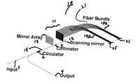
- FIG. 1is a schematic illustration of a variable optical delay line 10 in accordance with the invention.
- the delay line 10comprises an optical switch 11 such as a micromechanical mirror switch (MEMs switch) composed of a controllable scanning mirror 12 and a mirror array 13 .
- the delay linefurther includes one or more fiber arrays 14 A and 14 B of fiber delay paths.
- each fiber arraycomprises a plurality of fiber paths.
- Each fiber pathcomprises a curved region 21 where the fiber is curved differently from the other fibers in the array, a second region 22 where the fiber is parallel to other fibers in the array, and a reflector 25 .
- the arrayis designed so that each fiber path will reflect an input signal with a different delay than the other paths in the array.
- An array of collimator lenses(now shown) couples light in and out of the fiber array.
- Suitable MEMs mirror switches and their fabricationare described, for example, in U.S. Pat. No. 5,629,7990 issued to Nukermans et al. On May 13, 1997 which is incorporated herein by reference. Suitable switches are also described in U.S. application Ser. No. 09/415,178 filed by V. Aksyuk on Nov. 8, 1999 and Ser. No. 09/559,216 filed by Greywall on Apr. 26, 2000, both of which are incorporated herein by reference. Alternatively, waveguide switches can be used.
- FIG. 2is a top view of an exemplary fiber array, e.g. array 14 A, composed of a plurality of optical fiber paths 20 A, 20 B, . . . , 20 Z.
- Each fiber pathcan comprise three fiber regions 22 A, 21 and 22 B.
- Each fiber 20begins in a first linear array 23 and ends in a second linear array 24 . Between the beginning and the end, the fibers have different curvatures so that their respective optical path lengths are different.
- the fibersare substantially parallel, as in a multifiber ribbon.
- each fiberincludes one or more reflective elements such as Bragg gratings.
- fiber path 20 Ahas gratings 25 A and 26 A.
- fiber path 20 Zhas gratings 25 Z and 26 Z.
- the Bragg gratingsare preferably switchable between reflection and transmission.
- This fiber arraypresents important advantages in manufacture.
- the arraycan be readily fabricated as a computer generated optical fiber circuit using techniques well known in the art.
- a computerguides the point-by-point placement of fibers 20 A, 20 B, . . . , 20 Z on an adhesive-coated substrate 19 .
- This processis described in detail in U.S. Pat. No. 5,259,051 issued to J. Burack et al. On Nov. 2, 1993 and U.S. Pat. No. 5,421,970 issued to W. Holland on Jun. 6, 1995, which are incorporated herein by reference.
- the reflectors 25can be Bragg gratings conventionally formed in the fibers by conventional methods such as by sidewriting with ultraviolet light.
- An important advantage of the parallel orientation of the fibers in region 22 Bis that the gratings can be aligned along the same transverse section of a fiber ribbon. This has the important effect that all gratings across a ribbon, e.g. 25 A, 25 B, 25 Z, can all be formed in a single UV exposure.
- the reflector gratings 25can be made switchable by any one of a wide variety of techniques.
- the gratingscan be switched by magnetically, thermally, piezoelectrically or by magnetostriction.
- the preferred methodis by use of magnetic strain tuning using latchable magnets.
- Exemplary switchable gratingsare described, for example, in U.S. Pat. No. 6,154,590 issued to S. Jin et al. On Nov. 28, 2000; U.S. Pat. No. 6,128,427 issued to Espindola et al. On Oct. 3, 2000; U.S. Pat. No. 5,987,200 issued to Fleming et al. On Nov. 16, 1999; and U.S. Pat. No. 6,122,421 issued to Adams et al. On Sep. 19, 2000. All of these patents are incorporated herein by reference.
- the reflectors 25can be mechanically movable mirrors.
- An input optical signalcan be applied via an input fiber 1 . It passes through an optical circulator 2 and strikes scanning mirror 12 . Mirror 12 is controlled to direct the signal to the mirror of array 13 which will reflect the input signal into the fiber path of a fiber array that provides the desired delay. The signal propagates into the fiber path and is reflected by the first operational reflector in the path. Upon reflection, the signal reemerges from the fiber path, reflects from the mirrors 13 and 12 , passes through the collimator 3 , and is redirected by circulator 2 to an output fiber 4 . Between the circulator 2 and the reflectors 25 , the input and output signals share a common path 15 .
- each fiber pathincludes a plurality of separately switchable reflectors, e.g. 25 A, 26 A of path 20 A. Successive reflectors can be used to achieve coarse delay increments. Selection of particular fibers can provide fine delay increments.
- the advantages of this deviceare manifold.
- the delay lineis fast and provides arbitrarily small delay time increments. It is easily scalable to longer delay times, has low insertion loss, has coarse and fine control, and is suitable for batch manufacture.
- FIG. 3illustrates an alternative embodiment of a variable optical delay line similar to that of FIG. 1 except that scanning mirror 12 has been replaced by a second mirror array 33 and the single input/output path 15 of FIG. 1 has been replaced by a plurality of input/output paths 35 .
- each of the input beamscan be switched among a plurality of delay fibers in an array 34 , each fiber providing a different delay.
- the collimators and circulatorshave been omitted for clarity of illustration.
- FIG. 3is particularly useful as a multiwavelength optical communication system wherein different wavelength channels may require different delays, as might be required to perform switching.
- the different wavelength channelscan be provided on different input fibers and switched to different delay fibers providing the delay needed for each respective wavelength channel.
- the mirrors of the arrayscan be reoriented to redirect the input wavelength channels and thereby adjust the delay spectrum they experience.
Landscapes
- Physics & Mathematics (AREA)
- General Physics & Mathematics (AREA)
- Optics & Photonics (AREA)
- Engineering & Computer Science (AREA)
- Signal Processing (AREA)
- Theoretical Computer Science (AREA)
- Mechanical Light Control Or Optical Switches (AREA)
Abstract
Description
- This application claims the benefit of U.S. Provisional Application Ser. No. 60/251,748 of identical title filed by the present inventors on Dec. 6, 2000, which is incorporated herein by reference.[0001]
- This invention relates to variable optical delay lines and, in particular, to a high resolution variable delay line where the time delay can be programmably selected from a plurality of closely spaced time periods.[0002]
- One of the major advances in communications in recent years has been the increased use of optical fiber systems for carrying large quantities of information with low distortion and low cost over great distances.[0003]
- Optical delay lines are important components in optical communications for switching streams of optical signals from one path to another. For example, optical delay lines are critical components in packet switching used in Internet applications. Delay lines are also the building blocks in the correlation filters used to recognize packet addresses. They are also used in the buffers which control the timing of signal routing. Delay lines are used for synchronizing data bits, for compensating differential dispersion between different optical paths, and for compensating differential delay between paths. Because of the dynamics of high-speed systems, different delays may be required at different times.[0004]
- A variable optical delay line typically comprises a plurality of optical fibers, each cut to a slightly different length, and a fiber switch to switch an input signal among them and thus control the delay. In principle this should work, but in practice it has serious shortcomings for high-speed systems. Cutting fibers to a precision of millimeters is difficult, and this difficulty limits the achievable accuracy of delay time. Moreover, a variable delay line having a large dynamic range will require many precisely cut fibers. It is not practical to provide sufficient precisely cut fibers to provide fine delay increments (high temporal resolution) over a large dynamic range. Accordingly there is a need for an improved variable optical delay line capable of providing high resolution over a large dynamic range.[0005]
- In accordance with the invention, a high-resolution variable optical delay line comprises an optical switch, such as an optical micromechanical mirror switch, and an array of delay fibers paths. Each delay fiber path in the array comprises a first region where the fiber is curved differently from the other fibers in the region, advantageously at least a second other region where the fiber is essentially parallel to the other fibers in the region, and a reflector. Each fiber is curved differently from the others in order that the fiber paths each provide a different delay. The reflector is advantageously disposed in a parallel region.[0006]
- The advantages, nature and various additional features of the invention will appear more fully upon consideration of the illustrative embodiments now to be described in detail in connection with the accompanying drawings. In the drawings:[0007]
- FIG. 1 is a schematic illustration of a variable optical delay line in accordance with the invention;[0008]
- FIG. 2 is a schematic top view of a simplified array of fiber paths useful in the delay line of FIG. 1; and[0009]
- FIG. 3 illustrates a second embodiment of a variable optical delay line.[0010]
- It is to be understood that these drawings are for purposes of illustrating the concepts of the invention and are not to scale.[0011]
- Referring to the drawings, FIG. 1 is a schematic illustration of a variable optical delay line[0012]10 in accordance with the invention. The delay line10 comprises an optical switch11 such as a micromechanical mirror switch (MEMs switch) composed of a controllable scanning mirror12 and a
mirror array 13. The delay line further includes one or more fiber arrays14A and14B of fiber delay paths. As will be shown below, each fiber array comprises a plurality of fiber paths. Each fiber path comprises acurved region 21 where the fiber is curved differently from the other fibers in the array, a second region22 where the fiber is parallel to other fibers in the array, and areflector 25. The array is designed so that each fiber path will reflect an input signal with a different delay than the other paths in the array. An array of collimator lenses (now shown) couples light in and out of the fiber array. - Suitable MEMs mirror switches and their fabrication are described, for example, in U.S. Pat. No. 5,629,7990 issued to Nukermans et al. On May 13, 1997 which is incorporated herein by reference. Suitable switches are also described in U.S. application Ser. No. 09/415,178 filed by V. Aksyuk on Nov. 8, 1999 and Ser. No. 09/559,216 filed by Greywall on Apr. 26, 2000, both of which are incorporated herein by reference. Alternatively, waveguide switches can be used.[0013]
- FIG. 2 is a top view of an exemplary fiber array, e.g. array[0014]14A, composed of a plurality of
optical fiber paths 20A,20B, . . . ,20Z. Each fiber path can comprise threefiber regions fiber 20 begins in a firstlinear array 23 and ends in a secondlinear array 24. Between the beginning and the end, the fibers have different curvatures so that their respective optical path lengths are different. - In[0015]
regions region 22B each fiber includes one or more reflective elements such as Bragg gratings. For example,fiber path 20A hasgratings gratings 25Z and26Z. The Bragg gratings are preferably switchable between reflection and transmission. - This fiber array presents important advantages in manufacture. The array can be readily fabricated as a computer generated optical fiber circuit using techniques well known in the art. In essence, a computer guides the point-by-point placement of[0016]
fibers 20A,20B, . . . ,20Z on an adhesive-coatedsubstrate 19. This process is described in detail in U.S. Pat. No. 5,259,051 issued to J. Burack et al. On Nov. 2, 1993 and U.S. Pat. No. 5,421,970 issued to W. Holland on Jun. 6, 1995, which are incorporated herein by reference. - The[0017]
reflectors 25 can be Bragg gratings conventionally formed in the fibers by conventional methods such as by sidewriting with ultraviolet light. An important advantage of the parallel orientation of the fibers inregion 22B is that the gratings can be aligned along the same transverse section of a fiber ribbon. This has the important effect that all gratings across a ribbon, e.g.25A,25B,25Z, can all be formed in a single UV exposure. - The[0018]
reflector gratings 25 can be made switchable by any one of a wide variety of techniques. The gratings can be switched by magnetically, thermally, piezoelectrically or by magnetostriction. The preferred method is by use of magnetic strain tuning using latchable magnets. - Exemplary switchable gratings are described, for example, in U.S. Pat. No. 6,154,590 issued to S. Jin et al. On Nov. 28, 2000; U.S. Pat. No. 6,128,427 issued to Espindola et al. On Oct. 3, 2000; U.S. Pat. No. 5,987,200 issued to Fleming et al. On Nov. 16, 1999; and U.S. Pat. No. 6,122,421 issued to Adams et al. On Sep. 19, 2000. All of these patents are incorporated herein by reference. Alternatively, the[0019]
reflectors 25 can be mechanically movable mirrors. - Referring to FIG. 1, the operation of the inventive variable delay line may now be explained. An input optical signal can be applied via an input fiber[0020]1. It passes through an
optical circulator 2 and strikes scanning mirror12. Mirror12 is controlled to direct the signal to the mirror ofarray 13 which will reflect the input signal into the fiber path of a fiber array that provides the desired delay. The signal propagates into the fiber path and is reflected by the first operational reflector in the path. Upon reflection, the signal reemerges from the fiber path, reflects from themirrors 13 and12, passes through the collimator3, and is redirected bycirculator 2 to an output fiber4. Between thecirculator 2 and thereflectors 25, the input and output signals share acommon path 15. - Advantageously each fiber path includes a plurality of separately switchable reflectors, e.g.[0021]25A,26A of
path 20A. Successive reflectors can be used to achieve coarse delay increments. Selection of particular fibers can provide fine delay increments. - The advantages of this device are manifold. The delay line is fast and provides arbitrarily small delay time increments. It is easily scalable to longer delay times, has low insertion loss, has coarse and fine control, and is suitable for batch manufacture.[0022]
- FIG. 3 illustrates an alternative embodiment of a variable optical delay line similar to that of FIG. 1 except that scanning mirror[0023]12 has been replaced by a
second mirror array 33 and the single input/output path 15 of FIG. 1 has been replaced by a plurality of input/output paths 35. With this embodiment, each of the input beams can be switched among a plurality of delay fibers in anarray 34, each fiber providing a different delay. The collimators and circulators have been omitted for clarity of illustration. - The embodiment of FIG. 3 is particularly useful as a multiwavelength optical communication system wherein different wavelength channels may require different delays, as might be required to perform switching. The different wavelength channels can be provided on different input fibers and switched to different delay fibers providing the delay needed for each respective wavelength channel. Moreover, if the switch configuration changes, the mirrors of the arrays can be reoriented to redirect the input wavelength channels and thereby adjust the delay spectrum they experience.[0024]
- It is to be understood that the above-described embodiments are illustrative of only a few of the many possible specific embodiments, which can represent applications of the principles of the invention. Numerous and varied other arrangements can be readily devised by those skilled in the art without departing from the spirit and scope of the invention.[0025]
Claims (11)
Priority Applications (1)
| Application Number | Priority Date | Filing Date | Title |
|---|---|---|---|
| US09/773,844US6934431B2 (en) | 2000-12-06 | 2001-02-01 | Variable optical delay lines and methods for making same |
Applications Claiming Priority (2)
| Application Number | Priority Date | Filing Date | Title |
|---|---|---|---|
| US25174800P | 2000-12-06 | 2000-12-06 | |
| US09/773,844US6934431B2 (en) | 2000-12-06 | 2001-02-01 | Variable optical delay lines and methods for making same |
Publications (2)
| Publication Number | Publication Date |
|---|---|
| US20020067877A1true US20020067877A1 (en) | 2002-06-06 |
| US6934431B2 US6934431B2 (en) | 2005-08-23 |
Family
ID=26941804
Family Applications (1)
| Application Number | Title | Priority Date | Filing Date |
|---|---|---|---|
| US09/773,844Expired - Fee RelatedUS6934431B2 (en) | 2000-12-06 | 2001-02-01 | Variable optical delay lines and methods for making same |
Country Status (1)
| Country | Link |
|---|---|
| US (1) | US6934431B2 (en) |
Cited By (23)
| Publication number | Priority date | Publication date | Assignee | Title |
|---|---|---|---|---|
| US20040075090A1 (en)* | 2001-03-02 | 2004-04-22 | Taylor Geoff W. | Modulation doped thyrisor and complementary transistors combination for a monolithic optoelectric integrated circuit |
| US20040079971A1 (en)* | 2000-04-24 | 2004-04-29 | The University Of Connecticut | Imaging array utilizing thyristor-based pixel elements |
| US20040079963A1 (en)* | 2002-10-25 | 2004-04-29 | The University Of Connecticut | Optoelectronic circuit employing a heterojunction thyristor device that performs high speed sampling |
| US20040079939A1 (en)* | 2002-10-25 | 2004-04-29 | The University Of Connecticut | Photonic serial digital-to-analog converter employing a heterojunction thyristor device |
| US20040079961A1 (en)* | 2002-10-25 | 2004-04-29 | The University Of Connecticut | Photonic digital-to-analog converter employing a plurality of heterojunction thyristor devices |
| US20040079954A1 (en)* | 2002-10-25 | 2004-04-29 | Taylor Geoff W. | Semiconductor devices employing at least one modulation doped quantum well structure and one or more etch stop layers for accurate contact formation |
| US20040082091A1 (en)* | 2002-10-25 | 2004-04-29 | Taylor Geoff W. | Method of fabricating semiconductor devices employing at least one modulation doped quantum well structure and one or more etch stop layers for accurate contact formation |
| US20040094760A1 (en)* | 2002-10-25 | 2004-05-20 | The University Of Connecticut | Optoelectronic circuit employing a heterojunction thyristor device to convert a digital optical signal to a digital electrical signal |
| US6760503B1 (en)* | 2001-04-12 | 2004-07-06 | Eric F. Hermann | Scalable optical router/switch and method of constructing thereof |
| US20040262593A1 (en)* | 2003-06-24 | 2004-12-30 | University Of Connecticut | Heterojunction thyristor-based amplifier |
| US20050018730A1 (en)* | 2003-07-25 | 2005-01-27 | The University Of Connecticut And Opel, Inc. | Semiconductor laser array device employing modulation doped quantum well structures |
| JP2005055912A (en)* | 2003-08-05 | 2005-03-03 | Lucent Technol Inc | Variable optical delay line with a large continuous tuning range |
| US20050121663A1 (en)* | 1996-10-16 | 2005-06-09 | Taylor Geoff W. | Apparatus and a method of fabricating inversion channel devices with precision gate doping for a monolithic integrated circuit |
| US20050141814A1 (en)* | 2003-12-30 | 2005-06-30 | The Boeing Company | Digitally controlled optical fiber delay line |
| US20050168247A1 (en)* | 2004-01-30 | 2005-08-04 | The Regents Of The University Of California | Electrical transient sampling system using a regenerative gain-clamped fiber optic delay line |
| US6954473B2 (en) | 2002-10-25 | 2005-10-11 | Opel, Inc. | Optoelectronic device employing at least one semiconductor heterojunction thyristor for producing variable electrical/optical delay |
| US6974969B2 (en) | 2003-01-13 | 2005-12-13 | The University Of Connecticut | P-type quantum-well-base bipolar transistor device employing interdigitated base and emitter formed with a capping layer |
| US20060141682A1 (en)* | 2002-10-25 | 2006-06-29 | The University Of Connecticut | Method of fabricating semiconductor devices employing at least one modulation doped quantum well structure and one or more etch stop layers for accurate contact formation |
| US20060141651A1 (en)* | 2002-10-25 | 2006-06-29 | The University Of Connecticut And Opel, Inc. | Method of fabricating semiconductor devices employing at least one modulation doped quantum well structure and one or more etch stop layers for accurate contact formation |
| US7333731B2 (en) | 2004-04-26 | 2008-02-19 | The University Of Connecticut | Multifunctional optoelectronic thyristor and integrated circuit and optical transceiver employing same |
| US7333733B2 (en) | 2002-10-25 | 2008-02-19 | The University Of Connecticut | Optoelectronic clock generator producing high frequency optoelectronic pulse trains with variable frequency and variable duty cycle and low jitter |
| US7385230B1 (en) | 2005-02-08 | 2008-06-10 | The University Of Connecticut | Modulation doped thyristor and complementary transistor combination for a monolithic optoelectronic integrated circuit |
| US20120288285A1 (en)* | 2011-05-12 | 2012-11-15 | Verizon Patent And Licensing Inc. | Variable dispersion compensator |
Families Citing this family (2)
| Publication number | Priority date | Publication date | Assignee | Title |
|---|---|---|---|---|
| US7515780B2 (en)* | 2006-10-25 | 2009-04-07 | Alcatel-Lucent Usa Inc. | System and method for fabricating an optical isolator |
| US8036503B2 (en)* | 2009-02-19 | 2011-10-11 | DFS Fitel LLC | Low loss optical delay line using a microfiber coil |
Citations (1)
| Publication number | Priority date | Publication date | Assignee | Title |
|---|---|---|---|---|
| US5729642A (en)* | 1995-10-02 | 1998-03-17 | The Boeing Company | N×N optical switch array using electro-optic and passive waveguide circuits on planar substrates |
Family Cites Families (4)
| Publication number | Priority date | Publication date | Assignee | Title |
|---|---|---|---|---|
| US4671605A (en)* | 1985-02-06 | 1987-06-09 | The United States Of America As Represented By The Secretary Of The Air Force | Length dependent, optical time delay/filter device for electrical signals |
| US5018816A (en)* | 1990-06-11 | 1991-05-28 | Amp Incorporated | Optical delay switch and variable delay system |
| IT1277397B1 (en)* | 1995-07-31 | 1997-11-10 | Pirelli Cavi S P A Ora Pirelli | WAVE LENGTH MULTIPLATION TELECOMMUNICATION SYSTEM AND METHOD WITH CONTROLLED OUTPUT CHANNEL SEPARATION |
| US6356377B1 (en)* | 1999-11-10 | 2002-03-12 | Agere Systems Guardian Corp. | Mems variable optical delay lines |
- 2001
- 2001-02-01USUS09/773,844patent/US6934431B2/ennot_activeExpired - Fee Related
Patent Citations (1)
| Publication number | Priority date | Publication date | Assignee | Title |
|---|---|---|---|---|
| US5729642A (en)* | 1995-10-02 | 1998-03-17 | The Boeing Company | N×N optical switch array using electro-optic and passive waveguide circuits on planar substrates |
Cited By (42)
| Publication number | Priority date | Publication date | Assignee | Title |
|---|---|---|---|---|
| US7176046B2 (en) | 1996-10-16 | 2007-02-13 | The University Of Connecticut | Apparatus and a method of fabricating inversion channel devices with precision gate doping for a monolithic integrated circuit |
| US20050121663A1 (en)* | 1996-10-16 | 2005-06-09 | Taylor Geoff W. | Apparatus and a method of fabricating inversion channel devices with precision gate doping for a monolithic integrated circuit |
| US20040079971A1 (en)* | 2000-04-24 | 2004-04-29 | The University Of Connecticut | Imaging array utilizing thyristor-based pixel elements |
| US7432539B2 (en) | 2000-04-24 | 2008-10-07 | The University Of Connecticut | Imaging method utilizing thyristor-based pixel elements |
| US20070257275A1 (en)* | 2000-04-24 | 2007-11-08 | Taylor Geoff W | Imaging Method Utilizing Thyristor-Based Pixel Elements |
| US7247892B2 (en) | 2000-04-24 | 2007-07-24 | Taylor Geoff W | Imaging array utilizing thyristor-based pixel elements |
| US20040075090A1 (en)* | 2001-03-02 | 2004-04-22 | Taylor Geoff W. | Modulation doped thyrisor and complementary transistors combination for a monolithic optoelectric integrated circuit |
| US7012274B2 (en) | 2001-03-02 | 2006-03-14 | The University Of Connecticut | Modulation doped thyristor and complementary transistors combination for a monolithic optoelectronic integrated circuit |
| US6760503B1 (en)* | 2001-04-12 | 2004-07-06 | Eric F. Hermann | Scalable optical router/switch and method of constructing thereof |
| US6841795B2 (en) | 2002-10-25 | 2005-01-11 | The University Of Connecticut | Semiconductor devices employing at least one modulation doped quantum well structure and one or more etch stop layers for accurate contact formation |
| US6995407B2 (en) | 2002-10-25 | 2006-02-07 | The University Of Connecticut | Photonic digital-to-analog converter employing a plurality of heterojunction thyristor devices |
| US20040079963A1 (en)* | 2002-10-25 | 2004-04-29 | The University Of Connecticut | Optoelectronic circuit employing a heterojunction thyristor device that performs high speed sampling |
| US20080135831A1 (en)* | 2002-10-25 | 2008-06-12 | Taylor Geoff W | Optoelectronic Circuit Employing a Heterojunction Thyristor Device to Convert a Digital Optical Signal to a Digital Electrical Signal |
| US6853014B2 (en) | 2002-10-25 | 2005-02-08 | The University Of Connecticut | Optoelectronic circuit employing a heterojunction thyristor device that performs high speed sampling |
| US7595516B2 (en) | 2002-10-25 | 2009-09-29 | The University Of Connecticut | Optoelectronic circuit employing a heterojunction thyristor device to convert a digital optical signal to a digital electrical signal |
| US6873273B2 (en) | 2002-10-25 | 2005-03-29 | The University Of Connecticut | Photonic serial digital-to-analog converter employing a heterojunction thyristor device |
| US20040094760A1 (en)* | 2002-10-25 | 2004-05-20 | The University Of Connecticut | Optoelectronic circuit employing a heterojunction thyristor device to convert a digital optical signal to a digital electrical signal |
| US7333733B2 (en) | 2002-10-25 | 2008-02-19 | The University Of Connecticut | Optoelectronic clock generator producing high frequency optoelectronic pulse trains with variable frequency and variable duty cycle and low jitter |
| US7332752B2 (en) | 2002-10-25 | 2008-02-19 | The University Of Connecticut | Optoelectronic circuit employing a heterojunction thyristor device to convert a digital optical signal to a digital electrical signal |
| US6954473B2 (en) | 2002-10-25 | 2005-10-11 | Opel, Inc. | Optoelectronic device employing at least one semiconductor heterojunction thyristor for producing variable electrical/optical delay |
| US7776753B2 (en) | 2002-10-25 | 2010-08-17 | University Of Connecticut | Method of fabricating semiconductor devices employing at least one modulation doped quantum well structure and one or more etch stop layers for accurate contact formation |
| US20040079939A1 (en)* | 2002-10-25 | 2004-04-29 | The University Of Connecticut | Photonic serial digital-to-analog converter employing a heterojunction thyristor device |
| US7556976B2 (en) | 2002-10-25 | 2009-07-07 | The University Of Connecticut | Method of fabricating semiconductor devices employing at least one modulation doped quantum well structure and one or more etch stop layers for accurate contact formation |
| US20040082091A1 (en)* | 2002-10-25 | 2004-04-29 | Taylor Geoff W. | Method of fabricating semiconductor devices employing at least one modulation doped quantum well structure and one or more etch stop layers for accurate contact formation |
| US7015120B2 (en) | 2002-10-25 | 2006-03-21 | The University Of Connecticut | Method of fabricating semiconductor devices employing at least one modulation doped quantum well structure and one or more etch stop layers for accurate contact formation |
| US20060141682A1 (en)* | 2002-10-25 | 2006-06-29 | The University Of Connecticut | Method of fabricating semiconductor devices employing at least one modulation doped quantum well structure and one or more etch stop layers for accurate contact formation |
| US20060141651A1 (en)* | 2002-10-25 | 2006-06-29 | The University Of Connecticut And Opel, Inc. | Method of fabricating semiconductor devices employing at least one modulation doped quantum well structure and one or more etch stop layers for accurate contact formation |
| US20040079954A1 (en)* | 2002-10-25 | 2004-04-29 | Taylor Geoff W. | Semiconductor devices employing at least one modulation doped quantum well structure and one or more etch stop layers for accurate contact formation |
| US20040079961A1 (en)* | 2002-10-25 | 2004-04-29 | The University Of Connecticut | Photonic digital-to-analog converter employing a plurality of heterojunction thyristor devices |
| US6974969B2 (en) | 2003-01-13 | 2005-12-13 | The University Of Connecticut | P-type quantum-well-base bipolar transistor device employing interdigitated base and emitter formed with a capping layer |
| US20040262593A1 (en)* | 2003-06-24 | 2004-12-30 | University Of Connecticut | Heterojunction thyristor-based amplifier |
| US6841806B1 (en) | 2003-06-24 | 2005-01-11 | The University Of Connecticut | Heterojunction thyristor-based amplifier |
| US6977954B2 (en) | 2003-07-25 | 2005-12-20 | University Of Connecticut | Semiconductor laser array device employing modulation doped quantum well structures |
| US20050018730A1 (en)* | 2003-07-25 | 2005-01-27 | The University Of Connecticut And Opel, Inc. | Semiconductor laser array device employing modulation doped quantum well structures |
| JP2005055912A (en)* | 2003-08-05 | 2005-03-03 | Lucent Technol Inc | Variable optical delay line with a large continuous tuning range |
| US7283708B2 (en) | 2003-12-30 | 2007-10-16 | The Boeing Company | Digitally controlled optical fiber delay line |
| US20050141814A1 (en)* | 2003-12-30 | 2005-06-30 | The Boeing Company | Digitally controlled optical fiber delay line |
| US20050168247A1 (en)* | 2004-01-30 | 2005-08-04 | The Regents Of The University Of California | Electrical transient sampling system using a regenerative gain-clamped fiber optic delay line |
| US7333731B2 (en) | 2004-04-26 | 2008-02-19 | The University Of Connecticut | Multifunctional optoelectronic thyristor and integrated circuit and optical transceiver employing same |
| US7385230B1 (en) | 2005-02-08 | 2008-06-10 | The University Of Connecticut | Modulation doped thyristor and complementary transistor combination for a monolithic optoelectronic integrated circuit |
| US20120288285A1 (en)* | 2011-05-12 | 2012-11-15 | Verizon Patent And Licensing Inc. | Variable dispersion compensator |
| US8643925B2 (en)* | 2011-05-12 | 2014-02-04 | Verizon Patent And Licensing Inc. | Variable dispersion compensator |
Also Published As
| Publication number | Publication date |
|---|---|
| US6934431B2 (en) | 2005-08-23 |
Similar Documents
| Publication | Publication Date | Title |
|---|---|---|
| US6934431B2 (en) | Variable optical delay lines and methods for making same | |
| US6005993A (en) | Deflection optical matrix switch | |
| CA2029171C (en) | Multiport optical devices | |
| US6631222B1 (en) | Reconfigurable optical switch | |
| US6701043B2 (en) | Arrayed waveguide grating having a reflective input coupling | |
| CA2394936C (en) | Wavelength cross-connect | |
| US20090297097A1 (en) | Reconfigurable optical switch | |
| US20050008285A1 (en) | Multi-channel optical switch | |
| US20050074204A1 (en) | Spectral plane method and apparatus for wavelength-selective optical switching | |
| CN1249820A (en) | Optical wavelength selective device including at least one Bragg-grating structure | |
| CA2458649A1 (en) | Free-space wavelength routing systems with interleaved channels | |
| US7212695B2 (en) | Variable optical delay line with a large continuous tuning range | |
| EP1162856B1 (en) | Free space optical switch with lenses for re-collimating the light | |
| US20040136645A1 (en) | Demultiplexer/multiplexer with a controlled variable path length device | |
| CA2355918C (en) | M x n optical matrix switch | |
| WO2003046629A1 (en) | System and method for multiplexing and demultiplexing optical signals using diffraction gratings | |
| US6766084B1 (en) | Coarse wave division multiplexer | |
| Yuan et al. | Optical switches | |
| US6591031B2 (en) | Optical switch with movable mirror | |
| WO2000041015A1 (en) | Dense wavelength division multiplexer using multiple reflection optical delay lines | |
| CN1616999B (en) | Optical device and movable reflector | |
| US6697549B2 (en) | Optical switch | |
| JP4182758B2 (en) | Optical add / drop device | |
| CA2270438A1 (en) | Optical matrix switch |
Legal Events
| Date | Code | Title | Description |
|---|---|---|---|
| AS | Assignment | Owner name:LUCENT TECHNOLOGIES INC., NEW JERSEY Free format text:ASSIGNMENT OF ASSIGNORS INTEREST;ASSIGNORS:BRAUN, LINDA M.;HOLLAND, WILLIAM ROBERT;LEGRANGE, JANE D.;REEL/FRAME:011839/0924;SIGNING DATES FROM 20010409 TO 20010430 | |
| FEPP | Fee payment procedure | Free format text:PAYOR NUMBER ASSIGNED (ORIGINAL EVENT CODE: ASPN); ENTITY STATUS OF PATENT OWNER: LARGE ENTITY | |
| FPAY | Fee payment | Year of fee payment:4 | |
| FPAY | Fee payment | Year of fee payment:8 | |
| AS | Assignment | Owner name:CREDIT SUISSE AG, NEW YORK Free format text:SECURITY INTEREST;ASSIGNOR:ALCATEL-LUCENT USA INC.;REEL/FRAME:030510/0627 Effective date:20130130 | |
| AS | Assignment | Owner name:ALCATEL-LUCENT USA INC., NEW JERSEY Free format text:MERGER;ASSIGNOR:LUCENT TECHNOLOGIES INC.;REEL/FRAME:032388/0405 Effective date:20081101 | |
| AS | Assignment | Owner name:BANK OF AMERICA NA, VIRGINIA Free format text:SECURITY INTEREST;ASSIGNOR:LGS INNOVATIONS LLC;REEL/FRAME:032579/0066 Effective date:20140331 Owner name:ALCATEL-LUCENT USA INC., NEW JERSEY Free format text:RELEASE OF SECURITY INTEREST;ASSIGNOR:CREDIT SUISSE AG;REEL/FRAME:032578/0931 Effective date:20140331 | |
| AS | Assignment | Owner name:LGS INNOVATIONS LLC, VIRGINIA Free format text:ASSIGNMENT OF ASSIGNORS INTEREST;ASSIGNOR:ALCATEL LUCENT;REEL/FRAME:032743/0584 Effective date:20140331 | |
| AS | Assignment | Owner name:ALCATEL-LUCENT USA INC., NEW JERSEY Free format text:RELEASE BY SECURED PARTY;ASSIGNOR:CREDIT SUISSE AG;REEL/FRAME:033949/0531 Effective date:20140819 | |
| REMI | Maintenance fee reminder mailed | ||
| AS | Assignment | Owner name:BANK OF AMERICA, N.A., NEW YORK Free format text:NOTICE OF GRANT OF SECURITY INTEREST IN PATENTS;ASSIGNOR:LGS INNOVATIONS LLC;REEL/FRAME:043254/0393 Effective date:20170718 | |
| LAPS | Lapse for failure to pay maintenance fees | Free format text:PATENT EXPIRED FOR FAILURE TO PAY MAINTENANCE FEES (ORIGINAL EVENT CODE: EXP.) | |
| STCH | Information on status: patent discontinuation | Free format text:PATENT EXPIRED DUE TO NONPAYMENT OF MAINTENANCE FEES UNDER 37 CFR 1.362 | |
| FP | Lapsed due to failure to pay maintenance fee | Effective date:20170823 | |
| AS | Assignment | Owner name:LGS INNOVATIONS LLC, VIRGINIA Free format text:RELEASE BY SECURED PARTY;ASSIGNOR:BANK OF AMERICA, N.A.;REEL/FRAME:049074/0094 Effective date:20190301 | |
| AS | Assignment | Owner name:LGS INNOVATIONS LLC, GEORGIA Free format text:RELEASE BY SECURED PARTY;ASSIGNOR:BANK OF AMERICA, N.A.;REEL/FRAME:049247/0557 Effective date:20190521 |