US20020058352A1 - Monolithic lead-salt infrared radiation detectors and methods of formation - Google Patents
Monolithic lead-salt infrared radiation detectors and methods of formationDownload PDFInfo
- Publication number
- US20020058352A1 US20020058352A1US09/976,723US97672301AUS2002058352A1US 20020058352 A1US20020058352 A1US 20020058352A1US 97672301 AUS97672301 AUS 97672301AUS 2002058352 A1US2002058352 A1US 2002058352A1
- Authority
- US
- United States
- Prior art keywords
- detector elements
- lead
- passivation layer
- electrical
- salt
- Prior art date
- Legal status (The legal status is an assumption and is not a legal conclusion. Google has not performed a legal analysis and makes no representation as to the accuracy of the status listed.)
- Granted
Links
- 238000000034methodMethods0.000titleclaimsdescription63
- 230000005855radiationEffects0.000titledescription21
- 230000015572biosynthetic processEffects0.000titledescription4
- 238000002161passivationMethods0.000claimsabstractdescription96
- 239000004020conductorSubstances0.000claimsdescription24
- 238000000576coating methodMethods0.000claimsdescription18
- 238000000151depositionMethods0.000claimsdescription18
- 229940056932lead sulfideDrugs0.000claimsdescription17
- 229910052981lead sulfideInorganic materials0.000claimsdescription17
- VYPSYNLAJGMNEJ-UHFFFAOYSA-NSilicium dioxideChemical compoundO=[Si]=OVYPSYNLAJGMNEJ-UHFFFAOYSA-N0.000claimsdescription16
- 239000011248coating agentSubstances0.000claimsdescription16
- GGYFMLJDMAMTAB-UHFFFAOYSA-NselanylideneleadChemical compound[Pb]=[Se]GGYFMLJDMAMTAB-UHFFFAOYSA-N0.000claimsdescription12
- 239000010931goldSubstances0.000claimsdescription8
- 239000000377silicon dioxideSubstances0.000claimsdescription8
- PCHJSUWPFVWCPO-UHFFFAOYSA-NgoldChemical compound[Au]PCHJSUWPFVWCPO-UHFFFAOYSA-N0.000claimsdescription5
- 229910052737goldInorganic materials0.000claimsdescription5
- 230000008878couplingEffects0.000claimsdescription4
- 238000010168coupling processMethods0.000claimsdescription4
- 238000005859coupling reactionMethods0.000claimsdescription4
- 235000012239silicon dioxideNutrition0.000claimsdescription4
- 229910001258titanium goldInorganic materials0.000claimsdescription4
- ZNKMCMOJCDFGFT-UHFFFAOYSA-Ngold titaniumChemical compound[Ti].[Au]ZNKMCMOJCDFGFT-UHFFFAOYSA-N0.000claimsdescription3
- 238000000059patterningMethods0.000claimsdescription3
- 230000001235sensitizing effectEffects0.000claimsdescription2
- 238000000992sputter etchingMethods0.000claimsdescription2
- 239000010410layerSubstances0.000description112
- 239000000463materialSubstances0.000description22
- 230000008569processEffects0.000description18
- 206010070834SensitisationDiseases0.000description8
- 230000008313sensitizationEffects0.000description8
- 230000008021depositionEffects0.000description7
- 238000001816coolingMethods0.000description6
- 239000011521glassSubstances0.000description6
- 229910052581Si3N4Inorganic materials0.000description5
- 238000010884ion-beam techniqueMethods0.000description5
- HQVNEWCFYHHQES-UHFFFAOYSA-Nsilicon nitrideChemical compoundN12[Si]34N5[Si]62N3[Si]51N64HQVNEWCFYHHQES-UHFFFAOYSA-N0.000description5
- YBNMDCCMCLUHBL-UHFFFAOYSA-N(2,5-dioxopyrrolidin-1-yl) 4-pyren-1-ylbutanoateChemical compoundC=1C=C(C2=C34)C=CC3=CC=CC4=CC=C2C=1CCCC(=O)ON1C(=O)CCC1=OYBNMDCCMCLUHBL-UHFFFAOYSA-N0.000description4
- OYLGJCQECKOTOL-UHFFFAOYSA-Lbarium fluorideChemical compound[F-].[F-].[Ba+2]OYLGJCQECKOTOL-UHFFFAOYSA-L0.000description4
- 229910001632barium fluorideInorganic materials0.000description4
- 238000001514detection methodMethods0.000description4
- 238000010438heat treatmentMethods0.000description4
- TWNQGVIAIRXVLR-UHFFFAOYSA-Noxo(oxoalumanyloxy)alumaneChemical compoundO=[Al]O[Al]=OTWNQGVIAIRXVLR-UHFFFAOYSA-N0.000description4
- 229920002120photoresistant polymerPolymers0.000description4
- 239000002244precipitateSubstances0.000description4
- 239000004094surface-active agentSubstances0.000description4
- KDLHZDBZIXYQEI-UHFFFAOYSA-NPalladiumChemical compound[Pd]KDLHZDBZIXYQEI-UHFFFAOYSA-N0.000description3
- 238000007792additionMethods0.000description3
- 229940024548aluminum oxideDrugs0.000description3
- 238000012217deletionMethods0.000description3
- 230000037430deletionEffects0.000description3
- 238000005516engineering processMethods0.000description3
- 238000005530etchingMethods0.000description3
- 238000003754machiningMethods0.000description3
- 238000001451molecular beam epitaxyMethods0.000description3
- 238000000206photolithographyMethods0.000description3
- 238000000623plasma-assisted chemical vapour depositionMethods0.000description3
- 229920001721polyimidePolymers0.000description3
- 238000006467substitution reactionMethods0.000description3
- UKUVVAMSXXBMRX-UHFFFAOYSA-N2,4,5-trithia-1,3-diarsabicyclo[1.1.1]pentaneChemical compoundS1[As]2S[As]1S2UKUVVAMSXXBMRX-UHFFFAOYSA-N0.000description2
- IJGRMHOSHXDMSA-UHFFFAOYSA-NAtomic nitrogenChemical compoundN#NIJGRMHOSHXDMSA-UHFFFAOYSA-N0.000description2
- VYZAMTAEIAYCRO-UHFFFAOYSA-NChromiumChemical compound[Cr]VYZAMTAEIAYCRO-UHFFFAOYSA-N0.000description2
- 229910000530Gallium indium arsenideInorganic materials0.000description2
- 239000004952PolyamideSubstances0.000description2
- 239000004642PolyimideSubstances0.000description2
- RTAQQCXQSZGOHL-UHFFFAOYSA-NTitaniumChemical compound[Ti]RTAQQCXQSZGOHL-UHFFFAOYSA-N0.000description2
- KXNLCSXBJCPWGL-UHFFFAOYSA-N[Ga].[As].[In]Chemical compound[Ga].[As].[In]KXNLCSXBJCPWGL-UHFFFAOYSA-N0.000description2
- WBFMCDAQUDITAS-UHFFFAOYSA-Narsenic triselenideChemical compound[Se]=[As][Se][As]=[Se]WBFMCDAQUDITAS-UHFFFAOYSA-N0.000description2
- 230000004888barrier functionEffects0.000description2
- 238000003486chemical etchingMethods0.000description2
- 238000006243chemical reactionMethods0.000description2
- 229910052804chromiumInorganic materials0.000description2
- 239000011651chromiumSubstances0.000description2
- 230000006870functionEffects0.000description2
- 239000007789gasSubstances0.000description2
- 238000009413insulationMethods0.000description2
- 239000011229interlayerSubstances0.000description2
- 229920002647polyamidePolymers0.000description2
- 239000000843powderSubstances0.000description2
- HBMJWWWQQXIZIP-UHFFFAOYSA-Nsilicon carbideChemical compound[Si+]#[C-]HBMJWWWQQXIZIP-UHFFFAOYSA-N0.000description2
- 229910010271silicon carbideInorganic materials0.000description2
- 239000000126substanceSubstances0.000description2
- 230000003746surface roughnessEffects0.000description2
- 229910052719titaniumInorganic materials0.000description2
- 239000010936titaniumSubstances0.000description2
- 230000009466transformationEffects0.000description2
- 238000000844transformationMethods0.000description2
- XLYOFNOQVPJJNP-UHFFFAOYSA-NwaterSubstancesOXLYOFNOQVPJJNP-UHFFFAOYSA-N0.000description2
- DGAQECJNVWCQMB-PUAWFVPOSA-MIlexoside XXIXChemical compoundC[C@@H]1CC[C@@]2(CC[C@@]3(C(=CC[C@H]4[C@]3(CC[C@@H]5[C@@]4(CC[C@@H](C5(C)C)OS(=O)(=O)[O-])C)C)[C@@H]2[C@]1(C)O)C)C(=O)O[C@H]6[C@@H]([C@H]([C@@H]([C@H](O6)CO)O)O)O.[Na+]DGAQECJNVWCQMB-PUAWFVPOSA-M0.000description1
- 229910000661Mercury cadmium tellurideInorganic materials0.000description1
- 241001465754MetazoaSpecies0.000description1
- XUIMIQQOPSSXEZ-UHFFFAOYSA-NSiliconChemical compound[Si]XUIMIQQOPSSXEZ-UHFFFAOYSA-N0.000description1
- 239000013504Triton X-100Substances0.000description1
- 229920004890Triton X-100Polymers0.000description1
- PQLZZALLLYUAKL-UHFFFAOYSA-N[Au].[Cr].[Ni]Chemical compound[Au].[Cr].[Ni]PQLZZALLLYUAKL-UHFFFAOYSA-N0.000description1
- PMRMTSSYYVAROU-UHFFFAOYSA-N[Ti].[Ni].[Au]Chemical compound[Ti].[Ni].[Au]PMRMTSSYYVAROU-UHFFFAOYSA-N0.000description1
- 238000005299abrasionMethods0.000description1
- 239000003082abrasive agentSubstances0.000description1
- 238000005270abrasive blastingMethods0.000description1
- 238000010521absorption reactionMethods0.000description1
- 229910052782aluminiumInorganic materials0.000description1
- XAGFODPZIPBFFR-UHFFFAOYSA-NaluminiumChemical compound[Al]XAGFODPZIPBFFR-UHFFFAOYSA-N0.000description1
- 229940052288arsenic trisulfideDrugs0.000description1
- QVGXLLKOCUKJST-UHFFFAOYSA-Natomic oxygenChemical compound[O]QVGXLLKOCUKJST-UHFFFAOYSA-N0.000description1
- 239000006121base glassSubstances0.000description1
- 230000008901benefitEffects0.000description1
- 238000005513bias potentialMethods0.000description1
- 238000005422blastingMethods0.000description1
- MCMSPRNYOJJPIZ-UHFFFAOYSA-Ncadmium;mercury;telluriumChemical compound[Cd]=[Te]=[Hg]MCMSPRNYOJJPIZ-UHFFFAOYSA-N0.000description1
- 230000008859changeEffects0.000description1
- RZVXOCDCIIFGGH-UHFFFAOYSA-Nchromium goldChemical compound[Cr].[Au]RZVXOCDCIIFGGH-UHFFFAOYSA-N0.000description1
- 230000002939deleterious effectEffects0.000description1
- 238000005566electron beam evaporationMethods0.000description1
- 238000000605extractionMethods0.000description1
- 239000010408filmSubstances0.000description1
- 230000004907fluxEffects0.000description1
- -1for exampleSubstances0.000description1
- WPYVAWXEWQSOGY-UHFFFAOYSA-Nindium antimonideChemical compound[Sb]#[In]WPYVAWXEWQSOGY-UHFFFAOYSA-N0.000description1
- 230000003993interactionEffects0.000description1
- 238000007737ion beam depositionMethods0.000description1
- 229940046892lead acetateDrugs0.000description1
- XCAUINMIESBTBL-UHFFFAOYSA-Nlead(ii) sulfideChemical compound[Pb]=SXCAUINMIESBTBL-UHFFFAOYSA-N0.000description1
- 238000001459lithographyMethods0.000description1
- 238000004519manufacturing processMethods0.000description1
- 230000000873masking effectEffects0.000description1
- 229910052751metalInorganic materials0.000description1
- 239000002184metalSubstances0.000description1
- 238000001465metallisationMethods0.000description1
- 239000000203mixtureSubstances0.000description1
- 229910052757nitrogenInorganic materials0.000description1
- 239000001301oxygenSubstances0.000description1
- 229910052760oxygenInorganic materials0.000description1
- 229910052763palladiumInorganic materials0.000description1
- 239000012071phaseSubstances0.000description1
- 238000001020plasma etchingMethods0.000description1
- 238000007747platingMethods0.000description1
- 238000001556precipitationMethods0.000description1
- 230000009467reductionEffects0.000description1
- IYKVLICPFCEZOF-UHFFFAOYSA-NselenoureaChemical compoundNC(N)=[Se]IYKVLICPFCEZOF-UHFFFAOYSA-N0.000description1
- 229910052710siliconInorganic materials0.000description1
- 239000010703siliconSubstances0.000description1
- 229910052708sodiumInorganic materials0.000description1
- 239000011734sodiumSubstances0.000description1
- 239000011343solid materialSubstances0.000description1
- 239000007790solid phaseSubstances0.000description1
- 230000000087stabilizing effectEffects0.000description1
- 239000000758substrateSubstances0.000description1
- 239000010409thin filmSubstances0.000description1
- 239000000080wetting agentSubstances0.000description1
Images


Classifications
- H—ELECTRICITY
- H10—SEMICONDUCTOR DEVICES; ELECTRIC SOLID-STATE DEVICES NOT OTHERWISE PROVIDED FOR
- H10F—INORGANIC SEMICONDUCTOR DEVICES SENSITIVE TO INFRARED RADIATION, LIGHT, ELECTROMAGNETIC RADIATION OF SHORTER WAVELENGTH OR CORPUSCULAR RADIATION
- H10F39/00—Integrated devices, or assemblies of multiple devices, comprising at least one element covered by group H10F30/00, e.g. radiation detectors comprising photodiode arrays
- H10F39/011—Manufacture or treatment of image sensors covered by group H10F39/12
- H—ELECTRICITY
- H10—SEMICONDUCTOR DEVICES; ELECTRIC SOLID-STATE DEVICES NOT OTHERWISE PROVIDED FOR
- H10F—INORGANIC SEMICONDUCTOR DEVICES SENSITIVE TO INFRARED RADIATION, LIGHT, ELECTROMAGNETIC RADIATION OF SHORTER WAVELENGTH OR CORPUSCULAR RADIATION
- H10F39/00—Integrated devices, or assemblies of multiple devices, comprising at least one element covered by group H10F30/00, e.g. radiation detectors comprising photodiode arrays
- H10F39/10—Integrated devices
- H10F39/12—Image sensors
- H10F39/18—Complementary metal-oxide-semiconductor [CMOS] image sensors; Photodiode array image sensors
- H10F39/184—Infrared image sensors
- H—ELECTRICITY
- H10—SEMICONDUCTOR DEVICES; ELECTRIC SOLID-STATE DEVICES NOT OTHERWISE PROVIDED FOR
- H10F—INORGANIC SEMICONDUCTOR DEVICES SENSITIVE TO INFRARED RADIATION, LIGHT, ELECTROMAGNETIC RADIATION OF SHORTER WAVELENGTH OR CORPUSCULAR RADIATION
- H10F77/00—Constructional details of devices covered by this subclass
- H10F77/10—Semiconductor bodies
- H10F77/12—Active materials
- H10F77/127—Active materials comprising only Group IV-VI or only Group II-IV-VI chalcogenide materials, e.g. PbSnTe
Definitions
- An infrared radiation detectorresponds to the thermal energy radiated by objects, such as animals, automobiles, and airplanes. This thermal energy is typically not visible to the human eye. Accordingly, by using an infrared radiation detector, objects that are not visible may be perceived and/or alternative views of visible objects may be obtained.
- Infrared radiation detectorsare typically composed of numerous detector elements, each of which detects a portion of the scene.
- the detector elementsmay be formed monolithically onto an integrated circuit that processes the signals from the detector elements or formed on their own substrate and then coupled to integrated circuit.
- Monolithic architectureshave advantages over hybrid architectures in that they require fewer processing steps and suffer fewer performance losses due to absorption.
- HCTMercury-Cadmium-Telluride
- InSbIndium Antimonide
- the present inventionprovides systems and methods that reduce and/or eliminate at least some of the disadvantages with the prior art. Accordingly, at least in certain embodiments, the present invention provides a monolithic, two-dimensional array of Lead-Salt detector elements that has acceptable performance without cryogenic cooling.
- a two-dimensional array of Lead-Salt detector elements monolithically formed on an integrated circuitincludes an integrated circuit, a Lead-Salt layer, and electrical couplers.
- the integrated circuitincludes a passivation layer and a plurality of electrical contacts, the passivation layer having vias to the electrical contacts.
- the Lead-Salt layeris formed upon the passivation layer, delineated, and sensitized, the delineations forming a plurality of detector elements.
- the electrical couplersare formed between the electrical contacts and the detector elements.
- a method for forming a two-dimensional array of Lead-Salt detector elements monolithically on an integrated circuitincludes providing an integrated circuit having a passivation layer covering a plurality of electrical contacts and depositing a Lead-Salt layer upon the passivation layer, the Lead-Salt layer having a first surface adjacent the passivation layer and a second surface opposite the first surface.
- the methodalso includes delineating the Lead-Salt layer into a plurality of detector elements and creating vias through the passivation layer to the electrical contacts.
- the methodadditionally includes forming electrical couplings between the electrical contacts and the detector elements and sensitizing the Lead-Salt layer.
- the present inventionhas several technical features.
- the inventionallows short range infrared (SWIR) and medium wavelength infrared (MWIR) detectors to be readily manufactured.
- the detector elementscan operate at or close to room temperature. Accordingly, the detectors can avoid the cost and complexity of cryogenic cooling.
- the detector elementsexhibit time constants on the order of one to ten microseconds, allowing a high frame rate, which may be useful for tracking applications where the scene varies rapidly.
- the detector elementsmay have a relatively small pitch, such as, for example, less than approximately thirty microns, which allows higher resolution at a fixed integrated circuit size and/or lower cost at a fixed array format. Moreover, this will allow for a reduction in the complexity of manufacturing optics for the detector.
- the processing of the Lead-Salt layersuch as by sensitization, etching with surfactants, using ion beam machining, and/or heat treatments, allows increased detectivity of the detector elements.
- some embodimentsmay contain one, some, or all of these technical features.
- FIG. 1illustrates an infrared detection system in accordance with one embodiment of the present invention
- FIG. 2provides a more detailed view of the focal plane array and the read-out integrated circuit for the system of FIG. 1;
- FIG. 3illustrates detector elements monolithically formed on a read-out integrated circuit in accordance with one embodiment of the present invention
- FIG. 4is a flowchart illustrating one embodiment of a method for forming the detector elements of FIG. 3;
- FIG. 5illustrates another embodiment of detector elements in accordance with the present invention
- FIG. 6is a flowchart illustrating one embodiment of a method for forming the detector elements of FIG. 5;
- FIG. 7illustrates another embodiment of detector elements in accordance with the present invention.
- FIG. 8is a flowchart illustrating one embodiment of a method for forming the detector elements of FIG. 7;
- FIG. 9illustrates another embodiment of detector elements in accordance with the present invention.
- FIG. 10is a flowchart illustrating one embodiment of a method for forming the detector elements of FIG. 9.
- FIG. 11is a flowchart illustrating one embodiment of a method for forming detector elements in accordance with one embodiment of the present invention.
- FIG. 1illustrates an infrared detection system 20 in accordance with one embodiment of the present invention.
- system 20receives infrared radiation 10 from a scene that is to be imaged and produces electrical signals that represent the scene.
- infrared radiationmeans any radiation emitted in the band between seven-tenths of a micron and one-thousand microns.
- system 20includes optics 30 , a chopper 40 , a focal plane array (FPA) 50 , and read-out integrated circuit (ROIC) 60 .
- Optics 30gathers the infrared radiation 10 from the scene and directs it toward chopper 40 .
- Chopper 40alternately allows the infrared radiation gathered by optics 30 and the infrared radiation of a reference scene, possibly the chopper itself, to impinge upon FPA 50 .
- FPA 50which includes a plurality of photoconductive detector elements (not shown) arranged in a two-dimensional array, detects the infrared radiation from the alternating actual scene and reference scene and produces signals representative of the infrared radiation in each scene.
- ROIC 60upon which FPA 50 is monolithically formed, detects the signals from the detector elements of FPA 50 , processes them, and inserts them on a data link 61 , so that they may be processed further, such as for image extraction or viewing on a display.
- system 20operates as a photoconductive detection system.
- a bias voltagewhich typically ranges from 0.1 V to 10 V, depending on the size of detector elements, is applied to the detector elements, by ROIC 60 or an external bias source.
- each detector elementreceives a signal proportional to a temperature flux applied across the common and input electrodes, creating a bias current.
- ROIC 60may then read the current off each electrode during the actual and reference scenes, the impinging radiation causing a change in current.
- FPA 50may have an array of 320 ⁇ 256 detector elements spaced on thirty micron centers, giving ROIC 60 over 87,000 detector elements to be accessed, although almost any other number of detector elements could be used.
- ROIC 60may access some or all of detector elements on a continuous basis. Upon receiving the signals, ROIC 60 subtracts the reference signals from the actual signals, amplifies, filters, adjusts gain, and multiplexes the analog signals. ROIC 60 can also perform other functions, such as, for example, A/D conversion, detector element substitution, and/or auto gain control.
- Optics 30may include a lens, a mirror, a polarizer, a beam splitter, and/or any other type of device for manipulating infrared radiation.
- Chopper 40may be a shutter, a rotating blade, or any other type of device for alternately allowing and not allowing infrared radiation 10 to impinge upon FPA 50 .
- ROIC 60may be any type of semiconductive device that detects and processes signals from detector elements of an FPA 50 .
- ROIC 60is a silicon-based CMOS multiplexer.
- Data link 61may be a bus, a fiber-optic cable, a wireless channel, or any other type of wireline or wireless link.
- FIG. 2provides a more detailed view of FPA 50 and ROIC 60 for system 20 .
- FPA 50includes a plurality of detector elements 52 arranged in a two-dimensional grid such that each of detector elements 52 receives the infrared radiation from part of the scene.
- the detector elements of FPA 50may be composed of any type of material that changes resistance when infrared radiation impinges thereon, in particular embodiments, they are composed of a Lead-Salt compound, such as, for example, Lead-Sulfide (PbS) or Lead-Selenide (PbSe).
- Detector elements 52are formed on ROIC 60 and, hence, the FPA 50 and ROIC 60 are monolithic because they are grown/fabricated on the same wafer.
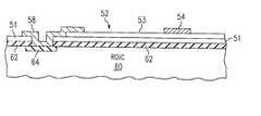
- FIG. 3illustrates detector elements 52 monolithically formed on ROIC 60 in accordance with one embodiment of the present invention.
- ROIC 60includes a passivation layer 62 that provides a surface upon which to form other structures and electrical contacts 64 (only one of which is shown) that allow the flow of electrical signals into ROIC 60 from each of detector elements 52 (only one of which is shown).
- passivation layer 62is approximately one and one-half microns thick and, in general, is between about one micron and two microns in thickness
- electrical contacts 64are approximately seven-tenths of a micron thick and, in general, are between about one-half micron and one micron in thickness.
- Each of detector elements 52includes part of a common grid 54 , which runs between the detector elements 52 of FPA 50 to provide an input signal to all of the detector elements, and one of electrical contacts 56 , which carries output signals. These structures are formed on passivation layer 62 . As shown, common grid 54 is approximately four-tenths of a micron thick and, in general, is between about two-tenths of a micron and one micron in thickness, and electrical contacts 56 are approximately four-tenths of a micron thick and, in general, are between about two-tenths of a micron and one micron in thickness. Each of detector elements 52 also includes a Lead-Salt layer 53 that serves to detect the impinging infrared radiation.
- Lead-Salt layer 53is partly formed on passivation layer 62 , one of electrical contacts 56 , and common grid 54 , and is approximately one micron thick. In general, Lead-Salt layer 53 is between about one micron and two microns in thickness.
- Each of detector elements 52additionally includes one of electrical couplers 58 to electrically couple the electrical contact 56 of the detector element to one of electrical contacts 64 of the ROIC 60 .
- electrical couplers 58are approximately four-tenths of a micron thick and, in general, may be between about two-tenths of a micron and one micron in thickness.
- Each of detector elements 52further includes a passivation layer 57 formed over Lead-Salt layer 53 and electrical couplers 58 .
- Passivation layer 57may assist in maintaining Lead-Salt stability and optimizing performance. As shown, passivation layer 57 is approximately one-half of a micron thick and, in general, may be between about two-tenths of a micron and four microns in thickness. Passivation layer 57 is not required in certain embodiments.
- a bias potentialis applied to detector elements 52 through common grid 54 , creating a bias current through electrical contacts 56 , electrical couplers 58 , and electrical contacts 64 to ROIC 60 . Then, when infrared radiation impinges upon one of detector elements 52 , the resistance of the detector element changes, which alters the current and thereby creates a signal. These changes in current are processed by ROIC 60 to extract the signal due to the impinging infrared radiation.
- FPA 50 and ROIC 60may be composed of a variety of materials.
- passivation layer 62may be composed of Silicon Dioxide (SiO 2 ), Silicon Nitride (Si 3 N 4 ), and/or any other suitable passivation material.
- Electrical contacts 64may be composed of aluminum (Al), Gold (Au), or any other appropriate conductive material.
- Lead-Salt layer 53may be composed of Lead-Sulfide or any other appropriate type of photoconductive Lead-Salt material.
- Common grid 54 and electrical contacts 56may be composed of Titanium-Gold (Ti—Au), Chromium-Gold (Cr—Au), Chromium-Nickel-Gold (Cr—Ni—Au), Titanium-Nickel-Gold (Ti—Ni—Au), or any other suitable conductive material.
- the Titanium and Chromiumprovide adhesion to the passivation layer 62
- the Goldprovides the Ohmic contact to the detector element that is subsequently deposited.
- Electrical couplers 58may be composed of Gold, Chromium, Titanium, Palladium (Pd), or any other appropriate conductive material.
- Passivation layer 57may be composed of Arsenic Tri-Sulfide (As 2 S 3 ), Arsenic Tri-Selenide (As 2 Se 3 ), Barium Fluoride (BaF 2 ), Silicon Nitride (Si 3 N 4 ), Polyimid, Silicon Dioxide (SiO 2 ), or any other appropriate passivating material.
- thermo-electric coolercan be used to increase performance by stabilizing the temperature of the device and/or cooling it to approximately two-hundred and fifty Kelvin. Cooling to the limit of the TEC, approximately one-hundred and eighty Kelvin, may further increase performance.
- FIG. 4is a flowchart 400 illustrating one embodiment of a method for forming detector elements 52 of FIG. 3.
- the methodbegins at step 404 by providing an ROIC with a passivation layer covering electrical contacts. This may be accomplished by obtaining an ROIC that has been fabricated through the passivation step without the final masking of the underlying electrical contacts.
- the passivation materialis usually chemically inert and, hence, provides a barrier to harmful materials such as Sodium and water. Thus, the electrical contacts should be protected from the chemical and/or thermal environments required to deposit and sensitize Lead-Salt detector elements.
- the methodcontinues at step 408 with the deposition of a conductive material upon the passivation layer.
- the conductive materialmay be deposited by Electron Beam Evaporation, by Ion Beam Deposition, or by any other appropriate process.
- the conductive materialis patterned at step 412 to form electrical contacts and a common grid for the detector elements. Patterning may be accomplished by lift-off photolithography, by etch back photolithography, or by any other appropriate process.
- the conductive materialis also aligned to the ROIC contacts using a contact aligner and photosensitive resists.
- a Lead-Sulfide layeris deposited upon the passivation layer and the conductive material at step 416 .
- the Lead-Sulfidemay be deposited by an aqueous precipitation growth process using a pH of over 13 , by Molecular Beam Epitaxy (MBE) Deposition, or any other appropriate process.
- MBEMolecular Beam Epitaxy
- multiple layers, such as, for example, two to five, of Lead-Sulfidemay need to be deposited to achieve desired performance characteristics.
- the Lead-Sulfide layeris delineated into numerous sections, each section corresponding to a detector element.
- the Lead-Sulfide layeris delineated into approximately sixteen micron by twenty-five micron sections, although other sizes could be used in other embodiments.
- Delineationmay be performed by chemical etching, ion beam etching, or any other appropriate process.
- surfactantsalso known as wetting agents, are used in the Lead-Salt chemical etching solutions at twenty-five degrees Celsius. Use of surfactants, such as, for example, Triton X-100, results in a significant decrease in undercutting, which leads to higher fill factor and the ability to reduce pitch.
- the detector elementsare separated by only about one micron.
- Viasare created through the passivation layer to expose the electrical contacts of the ROIC at step 424 . This may be accomplished by using a contact mask to selectively expose a layer of photoresist. The passivation layer is then etched, by using reactive ion etching, ion beam machining, or by any other appropriate process. The ROIC wirebond pads may be similarly exposed during this operation.
- a conductive materialis then deposited to form electrical couplers interconnecting the electrical contacts of the ROIC and the electrical contacts of the detector elements at step 428 .
- the conductive materialmay be deposited by thin film techniques, by lift-off metallization, or any other appropriate process. Thickness of the electrical couplers may be enhanced to greater than one micron using electrical plating through photoresist. In particular embodiments, a second common grid could also be formed on the detector elements during this step.
- the Lead-Sulfide layermay then be sensitized, which initiates and increases the detectivity of the detector elements, at step 432 .
- Sensitizationmay involve heating the device to between about 100° C. and 120° C. in an open-air oven for between about five hours and one-hundred hours.
- a passivation layeris deposited over the Lead-Sulfide and the electrical couplers.
- This passivation layermay be deposited using lift-off lithography, metal shadow mask techniques, or any other appropriate procedure.
- the passivation layermay be deposited by lift-off technology using multiple layers of resist to achieve a thickness to account for or cover nodules of the Lead-Salt and/or using reverse tapered reentrance profiles for the photoresist to reduce the material's tendency to stick to the sidewalls of the resist.
- the sensitization stepmay occur earlier in the process.
- the Lead-Salt layermay be removed as necessary to expose the passivation layer.
- the passivation layer over the detector elements and the electrical couplersdoes not have to be used.
- the conductive materialmay be selectively deposited upon the passivation layer, allowing the deletion of step 412 .
- the FPA 50may be subjected to a heat treatment, such as, for example, being heated to between about 180K and 260K for between approximately four minutes and twenty minutes before the deposition of the passivation layer. This may provide an increase in detectivity.
- a heat treatmentsuch as, for example, being heated to between about 180K and 260K for between approximately four minutes and twenty minutes before the deposition of the passivation layer. This may provide an increase in detectivity.
- an additional layer of insulation, passivation, or other appropriate materialmay be deposited upon the passivation layer of the ROIC before depositing the Lead-Salt layer.
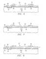
- FIG. 5illustrates another embodiment of detector elements 52 in accordance with the present invention.
- the embodiment illustrated by FIG. 5is similar to that illustrated by FIG. 3, in that ROIC 60 includes passivation layer 62 and electrical contacts 64 and each of detector elements 52 includes part of common grid 54 , one of electrical contacts 56 , Lead-Salt layer 53 , and one of electrical couplers 58 .
- electrical couplers 58electrically couple electrical contacts 64 to electrical contacts 56 .
- electrical couplers 58also overlay part of Lead-Salt layer 53 to provide an additional contact to the Lead-Salt layer 53 .
- each of detector elements 52includes part of a second common grid 59 that interconnects the detector elements 52 .
- Second common grid 59may provide better Ohmic contact than common grid 54 since the latter is covered by the Lead-Salt layer 53 .
- second common grid 59typically provides a bias voltage, similar to that carried by common grid 54 , to the detector elements.
- there is no passivation layer that covers Lead-Salt layer 53 and electrical contacts 58although one could be used.
- the components of the current embodimentmay be sized similarly to those in the embodiment illustrated by FIG. 3. Furthermore, the components of the current embodiment may be formed of materials similar to those used in the embodiment illustrated by FIG. 3.
- FIG. 6is a flowchart 600 illustrating one embodiment of a method for forming the detector elements illustrated by FIG. 5.
- the methodbegins at step 604 by providing an ROIC with a passivation layer covering the electrical contacts.
- the methodcontinues at step 608 with the deposition of a conductive material upon the passivation layer.
- the conductive materialis patterned at step 612 to form electrical contacts and a common grid for the detector elements.
- a Lead-Sulfide layeris deposited upon the passivation layer and the conductive material.
- the Lead-Sulfide layermay then be delineated into numerous sections to form the detector elements at step 620 .
- Viasare then formed through the passivation layer to expose the electrical contacts of the ROIC at step 624 .
- a conductive materialis deposited to form a second common grid between the detector elements and electrical couplers interconnecting the electrical contacts of the ROIC, the electrical contacts of the detector elements, and the detector elements.
- the deposition of the electrical couplers and/or the common grid on the Lead-Salt layermay be performed by lift-off technology using multiple layers of resist to achieve a thickness to account for or cover nodules of the Lead-Salt and/or reverse tapered reentrance profiles for the photoresist to reduce the material's tendency to stick to the sidewalls of the resist.
- the Lead-Sulfideis sensitized.
- a passivation layeris selectively deposited over the Lead-Sulfide layer, electrical couplers, and the second common grid at step 636 .
- FIG. 7illustrates another embodiment of detector elements 52 in accordance with the present invention.
- the current embodimentis similar to the embodiment illustrated by FIG. 5, in that ROIC 60 includes passivation layer 62 and electrical contacts 64 and each of detector elements 52 includes part of common grid 54 , Lead-Salt layer 53 , and one of electrical couplers 58 .
- electrical contacts 56are not present and, hence, electrical couplers 58 electrically couple Lead-Salt layer 53 to electrical contacts 64 . Accordingly, during operation, signals may flow directly into electrical couplers 58 .
- common grid 54is formed on top of Lead-Salt layer 53 , similar to second common grid 59 .
- the components of the current embodimentmay be sized similarly to those in the embodiment illustrated by FIG. 5. Furthermore, the components of the current embodiment may be formed of materials similar to those used in the embodiment illustrated by FIG. 5.
- FIG. 8is a flowchart 800 illustrating one embodiment of a method for forming the detector elements illustrated by FIG. 7.
- the methodbegins at step 804 by providing an ROIC with a passivation layer covering the electrical contacts.
- the methodcontinues at step 808 by depositing a Lead-Sulfide layer upon the passivation layer.
- the Lead-Sulfide layeris then delineated into detector elements at step 812 , and vias are formed through the passivation material to expose the electrical contacts of the ROIC at step 816 .
- a common grid between the detector elements and electrical couplers between the electrical contacts of the ROIC and the top of the detector elementsare formed at step 820 .
- the Lead-Sulfideis then sensitized at step 824 .
- a passivation layeris deposited over the Lead-Sulfide and electrical couplers at step 828 .
- FIG. 9illustrates another embodiment of detector elements 52 in accordance with the present invention. As can be seen, this embodiment is similar to that illustrated by FIG. 7. As before, ROIC 60 includes passivation layer 62 and electrical contacts 64 . Additionally, each of detector elements 52 includes Lead-Salt layer 53 , part of common grid 54 , and one of electrical couplers 58 . In this embodiment, however, each of detector elements 52 also includes a textured coating 51 between the passivation layer 62 and the Lead-Salt layer 53 . As shown, textured coating 51 is approximately two microns thick and, in general, may be between approximately one micron and five microns in thickness.
- electrical couplers 58extend from electrical contacts 64 over part of textured coating 51 and part of Lead-Salt layer 53 , similar to the embodiment illustrated in FIG. 7.
- electrical couplers 58may have a configuration similar to that in FIG. 3 or FIG. 5 or any other suitable configuration.
- the components of the current embodimentmay be sized similarly to those in the embodiment illustrated by FIG. 7. Furthermore, the components for the current embodiment may be composed of materials similar to those used in the embodiment illustrated by FIG. 7.
- the Lead-Salt layer 53is composed of Lead-Selenide.
- the Lead-Selenide layermay be formed on textured coating 51 by amorphous/polycrystalline chemically deposited using a precipitate method, which involves placing a wafer upside down in a heated solution of Lead Acetate and Selenourea with a pH between 6 - 7 , MBE, or by any other appropriate method.
- textured coating 51may be interlayers of Sio 2 precipitates, such as those produced by Strataglass, Inc. These interlayers are produced in a low pressure Plasma Enhanced Chemical Vapor Deposition (PECVD) whereby gas compositions at approximately 360° C. are altered to produce SiO 2 precipitates in the gas phase, rather than in the solid phase, on top of the ROIC. A subsequent one micron SiO 2 layer is deposited by PECVD to hold the precipitates in place. The textured surfaces produced achieves the surface roughness requirement for a uniform PbSe deposition.
- PECVDPlasma Enhanced Chemical Vapor Deposition
- textured coating 51could be a porous spin-on glass, such as that manufactured by Honeywell/Allied Signal, formed during the spin-on/bake cycle.
- textured coating 51may be spin-on glass consisting of solid materials suspended in an appropriate solution, resulting in a textured surface.
- An example of thisis the one-half micron spin-on glass made by Schott Glass Works or others such as Corning Glass Works.
- texturingmay be accomplished by using blasting abrasives, such as Silicon Carbide or Aluminum Oxide, on spin-on glass.
- Plasma and Ion Beamsmay be able to texture a glass surface after a base glass layer has been spun onto the wafer. This may require multiple spin-on coatings.
- textured polyamide coatingsmay be used. These may be formed by forming a polyamide coating with a thickness between three to five microns and abrading it to various surface roughness conditions.
- ten micron Aluminum Oxide abrasive powdersAlthough loss of photoconductivity, possibly due to interactions of the organic Polyimide with the PbSe during the >400° C. sensitization process, is a cause for concern.
- an addition of low temperature Silicon Nitride or other passivating materialmay provide a barrier between the PbSe and the Polyimide and thereby result in acceptable D* performance of the PbSe films. Additionally, combinations of the above may be used.
- the texturizing materialshould have one or more of the following characteristics: 1) good adhesion to the passivation layer of the ROIC; 2) a thermal expansion coefficient similar to that of the Lead-Salt layer; 3) good insulation resistance; 4) intertness to high pH chemicals; 5) controllable surface finish; 6) non-reactive when heated to sensitization temperatures; and 7) photodelineatable.
- FIG. 10is a flowchart 1000 illustrating a method for forming the detector elements illustrated by FIG. 9.
- the methodbegins at step 1004 by providing an ROIC with a passivation layer covering the electrical contacts.
- the methodcontinues at step 1008 by depositing a textured coating over the passivation layer.
- a Lead-Selenide layeris deposited upon the textured coating.
- the Lead-Selenide layeris then sensitized at step 1016 and delineated into detector elements at step 1020 .
- Sensitizationmay involve exposing the Lead-Selenide layer to Oxygen, Nitrogen, and/or Water Vapor at a relatively high temperature, such as, for example, greater than 400° C. or any other appropriate process. In particular embodiments, sensitization may occur after delineation. Vias are then created through the textured coating and the passivation material to expose the electrical contacts of the ROIC at step 1024 , and a common grid between the detector elements and electrical couplers between the electrical contacts and the top of the detector elements are formed at step 1028 . A passivation layer is selectively deposited over the Lead-Selenide layer and electrical couplers at step 1032 .
- FIG. 11is a flowchart 1100 illustrating the formation of detector elements 52 for this embodiment. The method begins at step 1104 by providing an ROIC with a passivation layer covering the electrical contacts. The method continues at step 1108 by texturizing the passivation layer.
- Texturizing of the passivation layermay be performed by patterning micron, and possible sub-micron, structures onto the passivation layer by photolithography followed by: 1) an ion milling process; 2) a plasma process; or 3) abrasive blasting of powders, such as Aluminum-Oxide (Al 2 O 3 ), Silicon Carbide, or any other particulate that produces adequate roughness on which to deposit, sensitize, and pattern Lead-Salts.
- a buffer layer of Barium Fluoride (BaF), glass, or other suitable materialis applied prior to the abrasion process.
- a Lead-Selenide layeris deposited upon the textured passivation layer.
- the Lead-Selenide layeris then sensitized at step 1116 and delineated into detector elements at step 1120 . Vias are created through the passivation layer to expose the electrical contacts of the ROIC at step 1124 . At step 1128 , a common grid between the detector elements and electrical couplers between the electrical contacts of the ROIC and the detector elements are formed. A passivation layer is deposited over the Lead-Salt layer and the electrical couplers at step 1132 .
- the detector elementsare especially useful in the short range infrared (SWIR) band (approximately one to three microns), and, in other embodiments, the detector elements are especially useful in the medium wavelength infrared (MWIR) band (approximately three to five microns).
- SWIR detectors and MWIR detectorsmay be readily manufactured.
- the detector elementscan operate at or close to room temperature. Accordingly, the detectors can avoid the cost and complexity of cryogenic cooling.
- the detector elementsexhibit time constants on the order of one to ten microseconds, allowing a high frame rate, which may be useful for tracking applications.
- the electrical contact patternsallow an acceptable fill factor to be obtained while maintaining good Ohmic contact. Moreover, with the electrical contact patterns, higher fill factors, over seventy percent, are probably obtainable, which would increase the efficiency of the detector, although shrinking the electrical contacts may result in problems in maintaining good Ohmic contact. Furthermore, the electrical contacts may be staggered, which will allow also an increase in fill factor. As an additional example, in certain embodiments, the detector elements 52 may have a relatively small pitch, such as, for example, less than approximately thirty microns, which allows for smaller FPAs for the same format and/or larger FPA formats, 640 ⁇ 480, for example, in the same integrated circuit space.
- the processing of the Lead-Salt layersuch as by sensitization, etching with surfactants, using ion beam machining, and/or heat treatments allows increased detectivity of the detector elements, on the order of D pk * ⁇ 8 ⁇ e 10 ⁇ cm ⁇ Hz w
- system 20While the invention has been discussed with respect to system 20 , it should be appreciated that the invention is useful in other infrared detection systems. These systems may or may not include optics 30 and/or chopper 40 . Additionally, these systems may include additional components, such as displays, feature extractors, and/or digital signal processors.
Landscapes
- Photometry And Measurement Of Optical Pulse Characteristics (AREA)
- Light Receiving Elements (AREA)
- Solid State Image Pick-Up Elements (AREA)
Abstract
Description
- An infrared radiation detector responds to the thermal energy radiated by objects, such as animals, automobiles, and airplanes. This thermal energy is typically not visible to the human eye. Accordingly, by using an infrared radiation detector, objects that are not visible may be perceived and/or alternative views of visible objects may be obtained.[0001]
- Infrared radiation detectors are typically composed of numerous detector elements, each of which detects a portion of the scene. The detector elements may be formed monolithically onto an integrated circuit that processes the signals from the detector elements or formed on their own substrate and then coupled to integrated circuit. Monolithic architectures have advantages over hybrid architectures in that they require fewer processing steps and suffer fewer performance losses due to absorption.[0002]
- Currently, several high performance monolithic, two-dimensional infrared detectors exist. These detectors typically have detector elements made of Mercury-Cadmium-Telluride (HCT) or Indium Antimonide (InSb), which are expensive and difficult to process. Moreover, to function properly, these detectors require cryogenic cooling, which is expensive to construct, complex to operate, and unreliable.[0003]
- There are two options for monolithic, two-dimensional infrared detectors that operate close to room temperature. In the eight to twelve micron band, microbolometer technologies are used. Unfortunately, these devices have a relatively long time constant—on the order of ten milliseconds. In the one to two micron band, Indium-Gallium-Arsenide (InGaAs) detector elements are used. Unfortunately, formation of these detectors requires complex Molecular Beam Epitaxy deposition.[0004]
- While other materials are known to exhibit acceptable photoconductive properties, creating monolithic detector elements may be difficult. For example, achieving an appropriate chemical reaction between the detector element material and the material on which the detector elements are to be formed may be difficult. Moreover, the surface on which the detector elements are to be formed may not have an appropriate geometry for the formation. Furthermore, the processes used to sensitize or pattern the detector elements may be deleterious to the integrated circuit.[0005]
- The present invention provides systems and methods that reduce and/or eliminate at least some of the disadvantages with the prior art. Accordingly, at least in certain embodiments, the present invention provides a monolithic, two-dimensional array of Lead-Salt detector elements that has acceptable performance without cryogenic cooling.[0006]
- In certain embodiments, a two-dimensional array of Lead-Salt detector elements monolithically formed on an integrated circuit includes an integrated circuit, a Lead-Salt layer, and electrical couplers. The integrated circuit includes a passivation layer and a plurality of electrical contacts, the passivation layer having vias to the electrical contacts. The Lead-Salt layer is formed upon the passivation layer, delineated, and sensitized, the delineations forming a plurality of detector elements. The electrical couplers are formed between the electrical contacts and the detector elements.[0007]
- In particular embodiments, a method for forming a two-dimensional array of Lead-Salt detector elements monolithically on an integrated circuit includes providing an integrated circuit having a passivation layer covering a plurality of electrical contacts and depositing a Lead-Salt layer upon the passivation layer, the Lead-Salt layer having a first surface adjacent the passivation layer and a second surface opposite the first surface. The method also includes delineating the Lead-Salt layer into a plurality of detector elements and creating vias through the passivation layer to the electrical contacts. The method additionally includes forming electrical couplings between the electrical contacts and the detector elements and sensitizing the Lead-Salt layer.[0008]
- The present invention has several technical features. For example, the invention allows short range infrared (SWIR) and medium wavelength infrared (MWIR) detectors to be readily manufactured. As another example, in certain embodiments, the detector elements can operate at or close to room temperature. Accordingly, the detectors can avoid the cost and complexity of cryogenic cooling. As a further example, in particular embodiments, the detector elements exhibit time constants on the order of one to ten microseconds, allowing a high frame rate, which may be useful for tracking applications where the scene varies rapidly. As still a further example, in some embodiments, the detector elements may have a relatively small pitch, such as, for example, less than approximately thirty microns, which allows higher resolution at a fixed integrated circuit size and/or lower cost at a fixed array format. Moreover, this will allow for a reduction in the complexity of manufacturing optics for the detector. As another example, in certain embodiments, the processing of the Lead-Salt layer, such as by sensitization, etching with surfactants, using ion beam machining, and/or heat treatments, allows increased detectivity of the detector elements. Of course, some embodiments may contain one, some, or all of these technical features.[0009]
- Other technical features will be readily apparent to one skilled in the art from the following figures, written description, and claims.[0010]
- The drawings described below provide a more detailed understanding of the present invention, especially when considered in light of the following written description, and of its technical features:[0011]
- FIG. 1 illustrates an infrared detection system in accordance with one embodiment of the present invention;[0012]
- FIG. 2 provides a more detailed view of the focal plane array and the read-out integrated circuit for the system of FIG. 1;[0013]
- FIG. 3 illustrates detector elements monolithically formed on a read-out integrated circuit in accordance with one embodiment of the present invention;[0014]
- FIG. 4 is a flowchart illustrating one embodiment of a method for forming the detector elements of FIG. 3;[0015]
- FIG. 5 illustrates another embodiment of detector elements in accordance with the present invention;[0016]
- FIG. 6 is a flowchart illustrating one embodiment of a method for forming the detector elements of FIG. 5;[0017]
- FIG. 7 illustrates another embodiment of detector elements in accordance with the present invention;[0018]
- FIG. 8 is a flowchart illustrating one embodiment of a method for forming the detector elements of FIG. 7;[0019]
- FIG. 9 illustrates another embodiment of detector elements in accordance with the present invention;[0020]
- FIG. 10 is a flowchart illustrating one embodiment of a method for forming the detector elements of FIG. 9; and[0021]
- FIG. 11 is a flowchart illustrating one embodiment of a method for forming detector elements in accordance with one embodiment of the present invention.[0022]
- FIG. 1 illustrates an[0023]
infrared detection system 20 in accordance with one embodiment of the present invention. In general,system 20 receivesinfrared radiation 10 from a scene that is to be imaged and produces electrical signals that represent the scene. As used herein, “infrared radiation” means any radiation emitted in the band between seven-tenths of a micron and one-thousand microns. - As illustrated,[0024]
system 20 includesoptics 30, achopper 40, a focal plane array (FPA)50, and read-out integrated circuit (ROIC)60.Optics 30 gathers theinfrared radiation 10 from the scene and directs it towardchopper 40.Chopper 40 alternately allows the infrared radiation gathered byoptics 30 and the infrared radiation of a reference scene, possibly the chopper itself, to impinge upon FPA50. FPA50, which includes a plurality of photoconductive detector elements (not shown) arranged in a two-dimensional array, detects the infrared radiation from the alternating actual scene and reference scene and produces signals representative of the infrared radiation in each scene.ROIC 60, upon which FPA50 is monolithically formed, detects the signals from the detector elements ofFPA 50, processes them, and inserts them on adata link 61, so that they may be processed further, such as for image extraction or viewing on a display. - Because of the detector elements of FPA[0025]50,
system 20 operates as a photoconductive detection system. In operation, a bias voltage, which typically ranges from 0.1 V to 10 V, depending on the size of detector elements, is applied to the detector elements, byROIC 60 or an external bias source. Thus, each detector element receives a signal proportional to a temperature flux applied across the common and input electrodes, creating a bias current.ROIC 60 may then read the current off each electrode during the actual and reference scenes, the impinging radiation causing a change in current. For example,FPA 50 may have an array of 320×256 detector elements spaced on thirty micron centers, givingROIC 60 over 87,000 detector elements to be accessed, although almost any other number of detector elements could be used. In particular embodiments,ROIC 60 may access some or all of detector elements on a continuous basis. Upon receiving the signals,ROIC 60 subtracts the reference signals from the actual signals, amplifies, filters, adjusts gain, and multiplexes the analog signals.ROIC 60 can also perform other functions, such as, for example, A/D conversion, detector element substitution, and/or auto gain control. - The components of[0026]
system 20 may have any of a variety of forms.Optics 30 may include a lens, a mirror, a polarizer, a beam splitter, and/or any other type of device for manipulating infrared radiation.Chopper 40 may be a shutter, a rotating blade, or any other type of device for alternately allowing and not allowinginfrared radiation 10 to impinge uponFPA 50.ROIC 60 may be any type of semiconductive device that detects and processes signals from detector elements of anFPA 50. In a particular embodiment,ROIC 60 is a silicon-based CMOS multiplexer.Data link 61 may be a bus, a fiber-optic cable, a wireless channel, or any other type of wireline or wireless link. - FIG. 2 provides a more detailed view of[0027]
FPA 50 andROIC 60 forsystem 20. As illustrated,FPA 50 includes a plurality ofdetector elements 52 arranged in a two-dimensional grid such that each ofdetector elements 52 receives the infrared radiation from part of the scene. While the detector elements ofFPA 50 may be composed of any type of material that changes resistance when infrared radiation impinges thereon, in particular embodiments, they are composed of a Lead-Salt compound, such as, for example, Lead-Sulfide (PbS) or Lead-Selenide (PbSe).Detector elements 52 are formed onROIC 60 and, hence, theFPA 50 andROIC 60 are monolithic because they are grown/fabricated on the same wafer. - FIG. 3 illustrates[0028]
detector elements 52 monolithically formed onROIC 60 in accordance with one embodiment of the present invention. As illustrated,ROIC 60 includes apassivation layer 62 that provides a surface upon which to form other structures and electrical contacts64 (only one of which is shown) that allow the flow of electrical signals intoROIC 60 from each of detector elements52 (only one of which is shown). As illustrated,passivation layer 62 is approximately one and one-half microns thick and, in general, is between about one micron and two microns in thickness, andelectrical contacts 64 are approximately seven-tenths of a micron thick and, in general, are between about one-half micron and one micron in thickness. Each ofdetector elements 52 includes part of acommon grid 54, which runs between thedetector elements 52 ofFPA 50 to provide an input signal to all of the detector elements, and one ofelectrical contacts 56, which carries output signals. These structures are formed onpassivation layer 62. As shown,common grid 54 is approximately four-tenths of a micron thick and, in general, is between about two-tenths of a micron and one micron in thickness, andelectrical contacts 56 are approximately four-tenths of a micron thick and, in general, are between about two-tenths of a micron and one micron in thickness. Each ofdetector elements 52 also includes a Lead-Salt layer 53 that serves to detect the impinging infrared radiation. As illustrated, Lead-Salt layer 53 is partly formed onpassivation layer 62, one ofelectrical contacts 56, andcommon grid 54, and is approximately one micron thick. In general, Lead-Salt layer 53 is between about one micron and two microns in thickness. Each ofdetector elements 52 additionally includes one ofelectrical couplers 58 to electrically couple theelectrical contact 56 of the detector element to one ofelectrical contacts 64 of theROIC 60. As shown,electrical couplers 58 are approximately four-tenths of a micron thick and, in general, may be between about two-tenths of a micron and one micron in thickness. Each ofdetector elements 52 further includes apassivation layer 57 formed over Lead-Salt layer 53 andelectrical couplers 58.Passivation layer 57 may assist in maintaining Lead-Salt stability and optimizing performance. As shown,passivation layer 57 is approximately one-half of a micron thick and, in general, may be between about two-tenths of a micron and four microns in thickness.Passivation layer 57 is not required in certain embodiments. - In operation, a bias potential is applied to[0029]
detector elements 52 throughcommon grid 54, creating a bias current throughelectrical contacts 56,electrical couplers 58, andelectrical contacts 64 toROIC 60. Then, when infrared radiation impinges upon one ofdetector elements 52, the resistance of the detector element changes, which alters the current and thereby creates a signal. These changes in current are processed byROIC 60 to extract the signal due to the impinging infrared radiation. - The components of[0030]
FPA 50 andROIC 60 may be composed of a variety of materials. For example,passivation layer 62 may be composed of Silicon Dioxide (SiO2), Silicon Nitride (Si3N4), and/or any other suitable passivation material.Electrical contacts 64 may be composed of aluminum (Al), Gold (Au), or any other appropriate conductive material. Lead-Salt layer 53 may be composed of Lead-Sulfide or any other appropriate type of photoconductive Lead-Salt material.Common grid 54 andelectrical contacts 56 may be composed of Titanium-Gold (Ti—Au), Chromium-Gold (Cr—Au), Chromium-Nickel-Gold (Cr—Ni—Au), Titanium-Nickel-Gold (Ti—Ni—Au), or any other suitable conductive material. For the listed materials, the Titanium and Chromium provide adhesion to thepassivation layer 62, and the Gold provides the Ohmic contact to the detector element that is subsequently deposited.Electrical couplers 58 may be composed of Gold, Chromium, Titanium, Palladium (Pd), or any other appropriate conductive material.Passivation layer 57 may be composed of Arsenic Tri-Sulfide (As2S3), Arsenic Tri-Selenide (As2Se3), Barium Fluoride (BaF2), Silicon Nitride (Si3N4), Polyimid, Silicon Dioxide (SiO2), or any other appropriate passivating material. - In particular embodiments, a thermo-electric cooler (TEC) can be used to increase performance by stabilizing the temperature of the device and/or cooling it to approximately two-hundred and fifty Kelvin. Cooling to the limit of the TEC, approximately one-hundred and eighty Kelvin, may further increase performance.[0031]
- Although a specific geometry is shown for[0032]
detector elements 52 in FIG. 3, it should be appreciated that, due to processing variations, the geometry of actual devices may vary slightly. Furthermore, different embodiments may use different lengths, widths, and/or thicknesses for Lead-Salt layer 53,common grid 54,electrical contacts 56,electrical couplers 58,passivation layer 62 and/orelectrical contacts 64, which would also alter the illustrated geometry. - FIG. 4 is a[0033]
flowchart 400 illustrating one embodiment of a method for formingdetector elements 52 of FIG. 3. The method begins atstep 404 by providing an ROIC with a passivation layer covering electrical contacts. This may be accomplished by obtaining an ROIC that has been fabricated through the passivation step without the final masking of the underlying electrical contacts. The passivation material is usually chemically inert and, hence, provides a barrier to harmful materials such as Sodium and water. Thus, the electrical contacts should be protected from the chemical and/or thermal environments required to deposit and sensitize Lead-Salt detector elements. - The method continues at[0034]
step 408 with the deposition of a conductive material upon the passivation layer. The conductive material may be deposited by Electron Beam Evaporation, by Ion Beam Deposition, or by any other appropriate process. The conductive material is patterned atstep 412 to form electrical contacts and a common grid for the detector elements. Patterning may be accomplished by lift-off photolithography, by etch back photolithography, or by any other appropriate process. In particular embodiments, the conductive material is also aligned to the ROIC contacts using a contact aligner and photosensitive resists. - A Lead-Sulfide layer is deposited upon the passivation layer and the conductive material at[0035]
step 416. The Lead-Sulfide may be deposited by an aqueous precipitation growth process using a pH of over13, by Molecular Beam Epitaxy (MBE) Deposition, or any other appropriate process. In particular embodiments, multiple layers, such as, for example, two to five, of Lead-Sulfide may need to be deposited to achieve desired performance characteristics. - At[0036]
step 420, the Lead-Sulfide layer is delineated into numerous sections, each section corresponding to a detector element. In the illustrated embodiment, the Lead-Sulfide layer is delineated into approximately sixteen micron by twenty-five micron sections, although other sizes could be used in other embodiments. Delineation may be performed by chemical etching, ion beam etching, or any other appropriate process. In certain embodiments, surfactants, also known as wetting agents, are used in the Lead-Salt chemical etching solutions at twenty-five degrees Celsius. Use of surfactants, such as, for example, Triton X-100, results in a significant decrease in undercutting, which leads to higher fill factor and the ability to reduce pitch. In particular embodiments, the detector elements are separated by only about one micron. - Vias are created through the passivation layer to expose the electrical contacts of the ROIC at[0037]
step 424. This may be accomplished by using a contact mask to selectively expose a layer of photoresist. The passivation layer is then etched, by using reactive ion etching, ion beam machining, or by any other appropriate process. The ROIC wirebond pads may be similarly exposed during this operation. - A conductive material is then deposited to form electrical couplers interconnecting the electrical contacts of the ROIC and the electrical contacts of the detector elements at[0038]
step 428. The conductive material may be deposited by thin film techniques, by lift-off metallization, or any other appropriate process. Thickness of the electrical couplers may be enhanced to greater than one micron using electrical plating through photoresist. In particular embodiments, a second common grid could also be formed on the detector elements during this step. - The Lead-Sulfide layer may then be sensitized, which initiates and increases the detectivity of the detector elements, at[0039]
step 432. Sensitization may involve heating the device to between about 100° C. and 120° C. in an open-air oven for between about five hours and one-hundred hours. - Finally, a passivation layer is deposited over the Lead-Sulfide and the electrical couplers. This passivation layer may be deposited using lift-off lithography, metal shadow mask techniques, or any other appropriate procedure. In particular embodiments, the passivation layer may be deposited by lift-off technology using multiple layers of resist to achieve a thickness to account for or cover nodules of the Lead-Salt and/or using reverse tapered reentrance profiles for the photoresist to reduce the material's tendency to stick to the sidewalls of the resist.[0040]
- Although a variety of operations have been discussed with respect to[0041]
flowchart 400, other methods in accordance with the present invention may have more, less, and/or different arrangements of steps. For example, the sensitization step may occur earlier in the process. As another example, if the delineation of the Lead-Salt layer to form individual detector elements does not expose the passivation layer of the ROIC over the electrical contacts of the ROIC, the Lead-Salt layer may be removed as necessary to expose the passivation layer. As a further example, the passivation layer over the detector elements and the electrical couplers does not have to be used. As still a further example, the conductive material may be selectively deposited upon the passivation layer, allowing the deletion ofstep 412. As an additional example, theFPA 50 may be subjected to a heat treatment, such as, for example, being heated to between about 180K and 260K for between approximately four minutes and twenty minutes before the deposition of the passivation layer. This may provide an increase in detectivity. As still another example, an additional layer of insulation, passivation, or other appropriate material may be deposited upon the passivation layer of the ROIC before depositing the Lead-Salt layer. - FIG. 5 illustrates another embodiment of[0042]
detector elements 52 in accordance with the present invention. As can be seen, the embodiment illustrated by FIG. 5 is similar to that illustrated by FIG. 3, in thatROIC 60 includespassivation layer 62 andelectrical contacts 64 and each ofdetector elements 52 includes part ofcommon grid 54, one ofelectrical contacts 56, Lead-Salt layer 53, and one ofelectrical couplers 58. Furthermore,electrical couplers 58 electrically coupleelectrical contacts 64 toelectrical contacts 56. In this embodiment, however,electrical couplers 58 also overlay part of Lead-Salt layer 53 to provide an additional contact to the Lead-Salt layer 53. Accordingly, during operation, signals produced by impinging infrared radiation may flow throughelectrical contacts 56 intoelectrical couplers 58 and/or directly intoelectrical couplers 58. Additionally, each ofdetector elements 52 includes part of a secondcommon grid 59 that interconnects thedetector elements 52. Secondcommon grid 59 may provide better Ohmic contact thancommon grid 54 since the latter is covered by the Lead-Salt layer 53. In operation, secondcommon grid 59 typically provides a bias voltage, similar to that carried bycommon grid 54, to the detector elements. Furthermore, there is no passivation layer that covers Lead-Salt layer 53 andelectrical contacts 58, although one could be used. - The components of the current embodiment may be sized similarly to those in the embodiment illustrated by FIG. 3. Furthermore, the components of the current embodiment may be formed of materials similar to those used in the embodiment illustrated by FIG. 3.[0043]
- The current embodiment of[0044]
detector elements 52 may be formed in a manner similar to that illustrated by FIG. 4. FIG. 6 is aflowchart 600 illustrating one embodiment of a method for forming the detector elements illustrated by FIG. 5. The method begins atstep 604 by providing an ROIC with a passivation layer covering the electrical contacts. The method continues at step608 with the deposition of a conductive material upon the passivation layer. The conductive material is patterned atstep 612 to form electrical contacts and a common grid for the detector elements. Atstep 616, a Lead-Sulfide layer is deposited upon the passivation layer and the conductive material. The Lead-Sulfide layer may then be delineated into numerous sections to form the detector elements atstep 620. Vias are then formed through the passivation layer to expose the electrical contacts of the ROIC atstep 624. Next, atstep 628, a conductive material is deposited to form a second common grid between the detector elements and electrical couplers interconnecting the electrical contacts of the ROIC, the electrical contacts of the detector elements, and the detector elements. The deposition of the electrical couplers and/or the common grid on the Lead-Salt layer may be performed by lift-off technology using multiple layers of resist to achieve a thickness to account for or cover nodules of the Lead-Salt and/or reverse tapered reentrance profiles for the photoresist to reduce the material's tendency to stick to the sidewalls of the resist. Atstep 632, the Lead-Sulfide is sensitized. Finally, a passivation layer is selectively deposited over the Lead-Sulfide layer, electrical couplers, and the second common grid atstep 636. - FIG. 7 illustrates another embodiment of[0045]
detector elements 52 in accordance with the present invention. The current embodiment is similar to the embodiment illustrated by FIG. 5, in thatROIC 60 includespassivation layer 62 andelectrical contacts 64 and each ofdetector elements 52 includes part ofcommon grid 54, Lead-Salt layer 53, and one ofelectrical couplers 58. In this embodiment, however,electrical contacts 56 are not present and, hence,electrical couplers 58 electrically couple Lead-Salt layer 53 toelectrical contacts 64. Accordingly, during operation, signals may flow directly intoelectrical couplers 58. Furthermore,common grid 54 is formed on top of Lead-Salt layer 53, similar to secondcommon grid 59. - The components of the current embodiment may be sized similarly to those in the embodiment illustrated by FIG. 5. Furthermore, the components of the current embodiment may be formed of materials similar to those used in the embodiment illustrated by FIG. 5.[0046]
- The current embodiment of[0047]
detector elements 52 may be formed in a manner similar to that illustrated by FIG. 6. FIG. 8 is aflowchart 800 illustrating one embodiment of a method for forming the detector elements illustrated by FIG. 7. The method begins at step804 by providing an ROIC with a passivation layer covering the electrical contacts. The method continues atstep 808 by depositing a Lead-Sulfide layer upon the passivation layer. The Lead-Sulfide layer is then delineated into detector elements atstep 812, and vias are formed through the passivation material to expose the electrical contacts of the ROIC atstep 816. A common grid between the detector elements and electrical couplers between the electrical contacts of the ROIC and the top of the detector elements are formed atstep 820. The Lead-Sulfide is then sensitized atstep 824. A passivation layer is deposited over the Lead-Sulfide and electrical couplers atstep 828. - FIG. 9 illustrates another embodiment of[0048]
detector elements 52 in accordance with the present invention. As can be seen, this embodiment is similar to that illustrated by FIG. 7. As before,ROIC 60 includespassivation layer 62 andelectrical contacts 64. Additionally, each ofdetector elements 52 includes Lead-Salt layer 53, part ofcommon grid 54, and one ofelectrical couplers 58. In this embodiment, however, each ofdetector elements 52 also includes atextured coating 51 between thepassivation layer 62 and the Lead-Salt layer 53. As shown, texturedcoating 51 is approximately two microns thick and, in general, may be between approximately one micron and five microns in thickness. - As illustrated,[0049]
electrical couplers 58 extend fromelectrical contacts 64 over part oftextured coating 51 and part of Lead-Salt layer 53, similar to the embodiment illustrated in FIG. 7. However, in other embodiments,electrical couplers 58 may have a configuration similar to that in FIG. 3 or FIG. 5 or any other suitable configuration. - The components of the current embodiment may be sized similarly to those in the embodiment illustrated by FIG. 7. Furthermore, the components for the current embodiment may be composed of materials similar to those used in the embodiment illustrated by FIG. 7.[0050]
- In particular embodiments, the Lead-[0051]
Salt layer 53 is composed of Lead-Selenide. The Lead-Selenide layer may be formed ontextured coating 51 by amorphous/polycrystalline chemically deposited using a precipitate method, which involves placing a wafer upside down in a heated solution of Lead Acetate and Selenourea with a pH between6-7, MBE, or by any other appropriate method. - In certain embodiments,[0052]
textured coating 51 may be interlayers of Sio2precipitates, such as those produced by Strataglass, Inc. These interlayers are produced in a low pressure Plasma Enhanced Chemical Vapor Deposition (PECVD) whereby gas compositions at approximately 360° C. are altered to produce SiO2precipitates in the gas phase, rather than in the solid phase, on top of the ROIC. A subsequent one micron SiO2layer is deposited by PECVD to hold the precipitates in place. The textured surfaces produced achieves the surface roughness requirement for a uniform PbSe deposition. - There are numerous other possible candidates for[0053]
textured coating 51. For example,textured coating 51 could be a porous spin-on glass, such as that manufactured by Honeywell/Allied Signal, formed during the spin-on/bake cycle. As another example,textured coating 51 may be spin-on glass consisting of solid materials suspended in an appropriate solution, resulting in a textured surface. An example of this is the one-half micron spin-on glass made by Schott Glass Works or others such as Corning Glass Works. As a further example, texturing may be accomplished by using blasting abrasives, such as Silicon Carbide or Aluminum Oxide, on spin-on glass. Furthermore, Plasma and Ion Beams may be able to texture a glass surface after a base glass layer has been spun onto the wafer. This may require multiple spin-on coatings. As an additional example, textured polyamide coatings may be used. These may be formed by forming a polyamide coating with a thickness between three to five microns and abrading it to various surface roughness conditions. One example of this is using ten micron Aluminum Oxide abrasive powders, although loss of photoconductivity, possibly due to interactions of the organic Polyimide with the PbSe during the >400° C. sensitization process, is a cause for concern. However, an addition of low temperature Silicon Nitride or other passivating material may provide a barrier between the PbSe and the Polyimide and thereby result in acceptable D* performance of the PbSe films. Additionally, combinations of the above may be used. - In general, the texturizing material should have one or more of the following characteristics: 1) good adhesion to the passivation layer of the ROIC; 2) a thermal expansion coefficient similar to that of the Lead-Salt layer; 3) good insulation resistance; 4) intertness to high pH chemicals; 5) controllable surface finish; 6) non-reactive when heated to sensitization temperatures; and 7) photodelineatable.[0054]
- The current embodiment of[0055]
detector elements 52 may be constructed in a manner similar to that illustrated in FIG. 8. FIG. 10 is aflowchart 1000 illustrating a method for forming the detector elements illustrated by FIG. 9. The method begins at step1004 by providing an ROIC with a passivation layer covering the electrical contacts. The method continues atstep 1008 by depositing a textured coating over the passivation layer. Atstep 1012, a Lead-Selenide layer is deposited upon the textured coating. The Lead-Selenide layer is then sensitized atstep 1016 and delineated into detector elements atstep 1020. Sensitization may involve exposing the Lead-Selenide layer to Oxygen, Nitrogen, and/or Water Vapor at a relatively high temperature, such as, for example, greater than 400° C. or any other appropriate process. In particular embodiments, sensitization may occur after delineation. Vias are then created through the textured coating and the passivation material to expose the electrical contacts of the ROIC at step1024, and a common grid between the detector elements and electrical couplers between the electrical contacts and the top of the detector elements are formed atstep 1028. A passivation layer is selectively deposited over the Lead-Selenide layer and electrical couplers atstep 1032. - An alternative embodiment similar to the one illustrated by FIG. 9 is formed by texturizing[0056]
passivation layer 62 ofROIC 60 prior to depositing Lead-Salt layer 53. This embodiment may be formed in a manner similar to that illustrated byflowchart 1000. FIG. 11 is aflowchart 1100 illustrating the formation ofdetector elements 52 for this embodiment. The method begins at step1104 by providing an ROIC with a passivation layer covering the electrical contacts. The method continues atstep 1108 by texturizing the passivation layer. Texturizing of the passivation layer may be performed by patterning micron, and possible sub-micron, structures onto the passivation layer by photolithography followed by: 1) an ion milling process; 2) a plasma process; or 3) abrasive blasting of powders, such as Aluminum-Oxide (Al2O3), Silicon Carbide, or any other particulate that produces adequate roughness on which to deposit, sensitize, and pattern Lead-Salts. In particular embodiments a buffer layer of Barium Fluoride (BaF), glass, or other suitable material is applied prior to the abrasion process. Atstep 1112, a Lead-Selenide layer is deposited upon the textured passivation layer. The Lead-Selenide layer is then sensitized atstep 1116 and delineated into detector elements atstep 1120. Vias are created through the passivation layer to expose the electrical contacts of the ROIC atstep 1124. Atstep 1128, a common grid between the detector elements and electrical couplers between the electrical contacts of the ROIC and the detector elements are formed. A passivation layer is deposited over the Lead-Salt layer and the electrical couplers atstep 1132. - The embodiments discussed above possess several technical features. For example, in some embodiments, the detector elements are especially useful in the short range infrared (SWIR) band (approximately one to three microns), and, in other embodiments, the detector elements are especially useful in the medium wavelength infrared (MWIR) band (approximately three to five microns). Thus, SWIR detectors and MWIR detectors may be readily manufactured. As another example, the detector elements can operate at or close to room temperature. Accordingly, the detectors can avoid the cost and complexity of cryogenic cooling. As a further example, in particular embodiments, the detector elements exhibit time constants on the order of one to ten microseconds, allowing a high frame rate, which may be useful for tracking applications. As still another example, the electrical contact patterns allow an acceptable fill factor to be obtained while maintaining good Ohmic contact. Moreover, with the electrical contact patterns, higher fill factors, over seventy percent, are probably obtainable, which would increase the efficiency of the detector, although shrinking the electrical contacts may result in problems in maintaining good Ohmic contact. Furthermore, the electrical contacts may be staggered, which will allow also an increase in fill factor. As an additional example, in certain embodiments, the[0057]
detector elements 52 may have a relatively small pitch, such as, for example, less than approximately thirty microns, which allows for smaller FPAs for the same format and/or larger FPA formats, 640×480, for example, in the same integrated circuit space. As another example, in some embodiments, the processing of the Lead-Salt layer, such as by sensitization, etching with surfactants, using ion beam machining, and/or heat treatments allows increased detectivity of the detector elements, on the order of
- at ambient temperatures for particular embodiments.[0058]
- While the invention has been discussed with respect to[0059]
system 20, it should be appreciated that the invention is useful in other infrared detection systems. These systems may or may not includeoptics 30 and/orchopper 40. Additionally, these systems may include additional components, such as displays, feature extractors, and/or digital signal processors. - Although several embodiments have been discussed for the present invention, a variety of additions, deletions, substitutions, and transformations will be readily suggested to those skilled in the art. Accordingly, the following claims are intended to encompass such additions, deletions, substitutions, and/or transformations.[0060]

Claims (31)
Priority Applications (1)
| Application Number | Priority Date | Filing Date | Title |
|---|---|---|---|
| US09/976,723US6734516B2 (en) | 2000-10-13 | 2001-10-11 | Monolithic lead-salt infrared radiation detectors and methods of formation |
Applications Claiming Priority (2)
| Application Number | Priority Date | Filing Date | Title |
|---|---|---|---|
| US24052500P | 2000-10-13 | 2000-10-13 | |
| US09/976,723US6734516B2 (en) | 2000-10-13 | 2001-10-11 | Monolithic lead-salt infrared radiation detectors and methods of formation |
Publications (2)
| Publication Number | Publication Date |
|---|---|
| US20020058352A1true US20020058352A1 (en) | 2002-05-16 |
| US6734516B2 US6734516B2 (en) | 2004-05-11 |
Family
ID=22906890
Family Applications (2)
| Application Number | Title | Priority Date | Filing Date |
|---|---|---|---|
| US09/976,723Expired - Fee RelatedUS6734516B2 (en) | 2000-10-13 | 2001-10-11 | Monolithic lead-salt infrared radiation detectors and methods of formation |
| US09/976,191Expired - LifetimeUS6690012B1 (en) | 2000-10-13 | 2001-10-11 | Hybridized lead-salt infrared radiation detectors and methods of formation |
Family Applications After (1)
| Application Number | Title | Priority Date | Filing Date |
|---|---|---|---|
| US09/976,191Expired - LifetimeUS6690012B1 (en) | 2000-10-13 | 2001-10-11 | Hybridized lead-salt infrared radiation detectors and methods of formation |
Country Status (5)
| Country | Link |
|---|---|
| US (2) | US6734516B2 (en) |
| EP (1) | EP1328964A4 (en) |
| AU (1) | AU2002213108A1 (en) |
| IL (2) | IL155223A0 (en) |
| WO (1) | WO2002031864A1 (en) |
Cited By (36)
| Publication number | Priority date | Publication date | Assignee | Title |
|---|---|---|---|---|
| US6690012B1 (en)* | 2000-10-13 | 2004-02-10 | Litton Systems, Inc. | Hybridized lead-salt infrared radiation detectors and methods of formation |
| WO2006072640A1 (en)* | 2004-12-29 | 2006-07-13 | Ministerio De Defensa | Method of treating polycrystalline lead selenide infrared detectors |
| US20070170363A1 (en)* | 2006-01-26 | 2007-07-26 | Schimert Thomas R | Infrared detector elements and methods of forming same |
| US20070205366A1 (en)* | 2004-06-03 | 2007-09-06 | Gidseg Ronald A | Laser Beam Steering System And Method For Use In A Directional Infrared Countermeasures System |
| US20110044011A1 (en)* | 2009-08-21 | 2011-02-24 | Tdk Corporation | Electronic component and manufacturing method thereof |
| US8153980B1 (en) | 2006-11-30 | 2012-04-10 | L-3 Communications Corp. | Color correction for radiation detectors |
| WO2012170946A3 (en)* | 2011-06-10 | 2013-05-23 | Flir Systems, Inc. | Low power and small form factor infrared imaging |
| WO2014137748A1 (en)* | 2013-03-06 | 2014-09-12 | The Board Of Regents Of The University Of Oklahoma | Pb-salt mid-infrared detectors and method for making same |
| US9058653B1 (en) | 2011-06-10 | 2015-06-16 | Flir Systems, Inc. | Alignment of visible light sources based on thermal images |
| US9235023B2 (en) | 2011-06-10 | 2016-01-12 | Flir Systems, Inc. | Variable lens sleeve spacer |
| US20160111567A1 (en)* | 2012-12-13 | 2016-04-21 | Board Of Regents University Of Oklahoma | Photovoltaic Lead-Salt Detectors |
| US9509924B2 (en) | 2011-06-10 | 2016-11-29 | Flir Systems, Inc. | Wearable apparatus with integrated infrared imaging module |
| US9706137B2 (en) | 2011-06-10 | 2017-07-11 | Flir Systems, Inc. | Electrical cabinet infrared monitor |
| US9706138B2 (en) | 2010-04-23 | 2017-07-11 | Flir Systems, Inc. | Hybrid infrared sensor array having heterogeneous infrared sensors |
| US9716843B2 (en) | 2009-06-03 | 2017-07-25 | Flir Systems, Inc. | Measurement device for electrical installations and related methods |
| US9756264B2 (en) | 2009-03-02 | 2017-09-05 | Flir Systems, Inc. | Anomalous pixel detection |
| US9807319B2 (en) | 2009-06-03 | 2017-10-31 | Flir Systems, Inc. | Wearable imaging devices, systems, and methods |
| US9843742B2 (en)* | 2009-03-02 | 2017-12-12 | Flir Systems, Inc. | Thermal image frame capture using de-aligned sensor array |
| US9848134B2 (en) | 2010-04-23 | 2017-12-19 | Flir Systems, Inc. | Infrared imager with integrated metal layers |
| US9887309B2 (en) | 2012-12-13 | 2018-02-06 | The Board of Regents of the University of Okalahoma | Photovoltaic lead-salt semiconductor detectors |
| US9948878B2 (en) | 2010-04-23 | 2018-04-17 | Flir Systems, Inc. | Abnormal clock rate detection in imaging sensor arrays |
| US9948872B2 (en) | 2009-03-02 | 2018-04-17 | Flir Systems, Inc. | Monitor and control systems and methods for occupant safety and energy efficiency of structures |
| US9961277B2 (en) | 2011-06-10 | 2018-05-01 | Flir Systems, Inc. | Infrared focal plane array heat spreaders |
| US9973692B2 (en) | 2013-10-03 | 2018-05-15 | Flir Systems, Inc. | Situational awareness by compressed display of panoramic views |
| US9986175B2 (en) | 2009-03-02 | 2018-05-29 | Flir Systems, Inc. | Device attachment with infrared imaging sensor |
| US10051210B2 (en) | 2011-06-10 | 2018-08-14 | Flir Systems, Inc. | Infrared detector array with selectable pixel binning systems and methods |
| US10169666B2 (en) | 2011-06-10 | 2019-01-01 | Flir Systems, Inc. | Image-assisted remote control vehicle systems and methods |
| US10321031B2 (en) | 2011-06-10 | 2019-06-11 | Flir Systems, Inc. | Device attachment with infrared imaging sensor |
| US10389953B2 (en) | 2011-06-10 | 2019-08-20 | Flir Systems, Inc. | Infrared imaging device having a shutter |
| US10539502B2 (en) | 2015-04-27 | 2020-01-21 | Flir Systems, Inc. | Moisture measurement device with thermal imaging capabilities and related methods |
| US10757308B2 (en) | 2009-03-02 | 2020-08-25 | Flir Systems, Inc. | Techniques for device attachment with dual band imaging sensor |
| US10841508B2 (en) | 2011-06-10 | 2020-11-17 | Flir Systems, Inc. | Electrical cabinet infrared monitor systems and methods |
| US10996542B2 (en) | 2012-12-31 | 2021-05-04 | Flir Systems, Inc. | Infrared imaging system shutter assembly with integrated thermister |
| US11297264B2 (en) | 2014-01-05 | 2022-04-05 | Teledyne Fur, Llc | Device attachment with dual band imaging sensor |
| US11445131B2 (en) | 2009-06-03 | 2022-09-13 | Teledyne Flir, Llc | Imager with array of multiple infrared imaging modules |
| US11514563B2 (en) | 2010-04-23 | 2022-11-29 | Flir Systems Ab | Infrared resolution and contrast enhancement with fusion |
Families Citing this family (13)
| Publication number | Priority date | Publication date | Assignee | Title |
|---|---|---|---|---|
| DE10132583A1 (en)* | 2001-07-05 | 2003-01-23 | Siemens Ag | Back-irradiable MSM module |
| US7045884B2 (en)* | 2002-10-04 | 2006-05-16 | International Rectifier Corporation | Semiconductor device package |
| EP1738413A4 (en)* | 2004-03-23 | 2008-05-28 | Bae Systems Information | MULTI-SPECTRAL NON-COOLED MICROBOLOMETER TYPE DETECTORS |
| US7742322B2 (en)* | 2005-01-07 | 2010-06-22 | Invisage Technologies, Inc. | Electronic and optoelectronic devices with quantum dot films |
| US7746681B2 (en)* | 2005-01-07 | 2010-06-29 | Invisage Technologies, Inc. | Methods of making quantum dot films |
| WO2005101530A1 (en) | 2004-04-19 | 2005-10-27 | Edward Sargent | Optically-regulated optical emission using colloidal quantum dot nanocrystals |
| US7773404B2 (en) | 2005-01-07 | 2010-08-10 | Invisage Technologies, Inc. | Quantum dot optical devices with enhanced gain and sensitivity and methods of making same |
| CA2519608A1 (en) | 2005-01-07 | 2006-07-07 | Edward Sargent | Quantum dot-polymer nanocomposite photodetectors and photovoltaics |
| US7262413B2 (en)* | 2005-03-14 | 2007-08-28 | Kauffman Christopher L | Photoconductive bolometer infrared detector |
| US7611920B1 (en)* | 2005-11-17 | 2009-11-03 | Bae Systems Information And Electronic Systems Integration Inc. | Photonic coupling scheme for photodetectors |
| US7592593B2 (en) | 2006-07-26 | 2009-09-22 | Northrop Grumman Corporation | Multi-band focal plane array |
| US7655496B1 (en)* | 2007-07-31 | 2010-02-02 | Flir Systems, Inc. | Metal lift-off systems and methods using liquid solvent and frozen gas |
| US9252182B2 (en) | 2012-09-05 | 2016-02-02 | Northrop Grumman Systems Corporation | Infrared multiplier for photo-conducting sensors |
Citations (6)
| Publication number | Priority date | Publication date | Assignee | Title |
|---|---|---|---|---|
| US4148052A (en)* | 1977-10-12 | 1979-04-03 | Westinghouse Electric Corp. | Radiant energy sensor |
| US4197633A (en)* | 1977-09-01 | 1980-04-15 | Honeywell, Inc. | Hybrid mosaic IR/CCD focal plane |
| US4206470A (en)* | 1977-09-01 | 1980-06-03 | Honeywell Inc. | Thin film interconnect for multicolor IR/CCD |
| US4570329A (en)* | 1984-08-15 | 1986-02-18 | Honeywell Inc. | Apparatus and method for fabricating backside mosaic of photoconductive infrared detectors |
| US4970567A (en)* | 1987-11-23 | 1990-11-13 | Santa Barbara Research Center | Method and apparatus for detecting infrared radiation |
| US5541438A (en)* | 1994-07-14 | 1996-07-30 | The United States Of America As Represented By The Secretary Of The Air Force | Backside illuminated MSM device |
Family Cites Families (35)
| Publication number | Priority date | Publication date | Assignee | Title |
|---|---|---|---|---|
| US3848261A (en)* | 1972-06-19 | 1974-11-12 | Trw Inc | Mos integrated circuit structure |
| US4339764A (en)* | 1977-05-27 | 1982-07-13 | The United States Of America As Represented By The Secretary Of The Navy | PbSx Se1-x semiconductor |
| US4472239A (en) | 1981-10-09 | 1984-09-18 | Honeywell, Inc. | Method of making semiconductor device |
| US4696188A (en) | 1981-10-09 | 1987-09-29 | Honeywell Inc. | Semiconductor device microstructure |
| US4624137A (en) | 1981-10-09 | 1986-11-25 | Honeywell Inc. | Semiconductor device |
| US4709252A (en)* | 1982-07-16 | 1987-11-24 | The United States Of America As Represented By The Administrator, National Aeronautics And Space Administration | Integrated photo-responsive metal oxide semiconductor circuit |
| US4825693A (en) | 1982-09-30 | 1989-05-02 | Honeywell Inc. | Slotted diaphragm semiconductor device |
| US4501144A (en) | 1982-09-30 | 1985-02-26 | Honeywell Inc. | Flow sensor |
| US4867842A (en) | 1982-09-30 | 1989-09-19 | Honeywell Inc. | Method of making slotted diaphragm semiconductor devices |
| US4478077A (en) | 1982-09-30 | 1984-10-23 | Honeywell Inc. | Flow sensor |
| US4683159A (en) | 1982-09-30 | 1987-07-28 | Honeywell Inc. | Semiconductor device structure and processing |
| US4478076A (en) | 1982-09-30 | 1984-10-23 | Honeywell Inc. | Flow sensor |
| US5220188A (en) | 1983-07-06 | 1993-06-15 | Honeywell Inc. | Integrated micromechanical sensor element |
| US5220189A (en) | 1983-07-06 | 1993-06-15 | Honeywell Inc. | Micromechanical thermoelectric sensor element |
| US4966037A (en) | 1983-09-12 | 1990-10-30 | Honeywell Inc. | Cantilever semiconductor device |
| US4806761A (en)* | 1985-04-08 | 1989-02-21 | Irvine Sensors Corporation | Thermal imager incorporating electronics module having focal plane sensor mosaic |
| US5450053A (en) | 1985-09-30 | 1995-09-12 | Honeywell Inc. | Use of vanadium oxide in microbolometer sensors |
| US4956686A (en)* | 1986-02-04 | 1990-09-11 | Texas Instruments Incorporated | Two color infrared focal plane array |
| US4682503A (en) | 1986-05-16 | 1987-07-28 | Honeywell Inc. | Microscopic size, thermal conductivity type, air or gas absolute pressure sensor |
| US5300915A (en) | 1986-07-16 | 1994-04-05 | Honeywell Inc. | Thermal sensor |
| US4752694A (en) | 1987-01-12 | 1988-06-21 | Honeywell Inc. | Array uniformity correction |
| WO1989005043A1 (en)* | 1987-11-23 | 1989-06-01 | Santa Barbara Research Center | Method and apparatus for detecting infrared radiation |
| US4914742A (en) | 1987-12-07 | 1990-04-03 | Honeywell Inc. | Thin film orthogonal microsensor for air flow and method |
| US5534111A (en) | 1988-02-29 | 1996-07-09 | Honeywell Inc. | Thermal isolation microstructure |
| US5286976A (en) | 1988-11-07 | 1994-02-15 | Honeywell Inc. | Microstructure design for high IR sensitivity |
| AU669548B2 (en) | 1992-06-19 | 1996-06-13 | Honeywell Inc. | Infrared camera with thermoelectric temperature stabilization |
| US6051846A (en)* | 1993-04-01 | 2000-04-18 | The United States Of America As Represented By The Secretary Of The Navy | Monolithic integrated high-Tc superconductor-semiconductor structure |
| US5561295A (en)* | 1994-07-29 | 1996-10-01 | Litton Systems, Inc. | Infrared-responsive photoconductive array and method of making |
| US5600143A (en)* | 1994-12-02 | 1997-02-04 | Litton Systems, Inc. | Sensor including an array of sensor elements and circuitry for individually adapting the sensor elements |
| US5665959A (en)* | 1995-01-13 | 1997-09-09 | The United States Of America As Represented By The Administrator Of The National Aeronautics And Space Adminstration | Solid-state image sensor with focal-plane digital photon-counting pixel array |
| FR2759494B1 (en)* | 1997-02-07 | 1999-03-05 | Commissariat Energie Atomique | MULTI-COLOR PHOTON RADIATION DETECTOR |
| US6005266A (en)* | 1997-03-13 | 1999-12-21 | The Trustees Of Princeton University | Very low leakage JFET for monolithically integrated arrays |
| US6413863B1 (en)* | 2000-01-24 | 2002-07-02 | Taiwan Semiconductor Manufacturing Company | Method to resolve the passivation surface roughness during formation of the AlCu pad for the copper process |
| IL155223A0 (en)* | 2000-10-13 | 2003-11-23 | Litton Systems Inc | Monolithic lead-salt infrared detectors |
| JP2002148342A (en)* | 2000-11-07 | 2002-05-22 | Canon Inc | Radiation imaging device |
- 2001
- 2001-10-10ILIL15522301Apatent/IL155223A0/enactiveIP Right Grant
- 2001-10-10AUAU2002213108Apatent/AU2002213108A1/ennot_activeAbandoned
- 2001-10-10EPEP01981468Apatent/EP1328964A4/ennot_activeWithdrawn
- 2001-10-10WOPCT/US2001/031761patent/WO2002031864A1/enactiveApplication Filing
- 2001-10-11USUS09/976,723patent/US6734516B2/ennot_activeExpired - Fee Related
- 2001-10-11USUS09/976,191patent/US6690012B1/ennot_activeExpired - Lifetime
- 2003
- 2003-06-04ILIL155223Apatent/IL155223A/ennot_activeIP Right Cessation
Patent Citations (6)
| Publication number | Priority date | Publication date | Assignee | Title |
|---|---|---|---|---|
| US4197633A (en)* | 1977-09-01 | 1980-04-15 | Honeywell, Inc. | Hybrid mosaic IR/CCD focal plane |
| US4206470A (en)* | 1977-09-01 | 1980-06-03 | Honeywell Inc. | Thin film interconnect for multicolor IR/CCD |
| US4148052A (en)* | 1977-10-12 | 1979-04-03 | Westinghouse Electric Corp. | Radiant energy sensor |
| US4570329A (en)* | 1984-08-15 | 1986-02-18 | Honeywell Inc. | Apparatus and method for fabricating backside mosaic of photoconductive infrared detectors |
| US4970567A (en)* | 1987-11-23 | 1990-11-13 | Santa Barbara Research Center | Method and apparatus for detecting infrared radiation |
| US5541438A (en)* | 1994-07-14 | 1996-07-30 | The United States Of America As Represented By The Secretary Of The Air Force | Backside illuminated MSM device |
Cited By (51)
| Publication number | Priority date | Publication date | Assignee | Title |
|---|---|---|---|---|
| US6690012B1 (en)* | 2000-10-13 | 2004-02-10 | Litton Systems, Inc. | Hybridized lead-salt infrared radiation detectors and methods of formation |
| US20070205366A1 (en)* | 2004-06-03 | 2007-09-06 | Gidseg Ronald A | Laser Beam Steering System And Method For Use In A Directional Infrared Countermeasures System |
| US7569824B2 (en) | 2004-06-03 | 2009-08-04 | Bae Systems Information And Electronic Systems Integration Inc. | Laser beam steering system and method for use in a directional infrared countermeasures system |
| WO2006072640A1 (en)* | 2004-12-29 | 2006-07-13 | Ministerio De Defensa | Method of treating polycrystalline lead selenide infrared detectors |
| US20080006774A1 (en)* | 2004-12-29 | 2008-01-10 | German Vergara Ogando | Method to process polycrystalline lead selenide infrared detectors |
| US20070170363A1 (en)* | 2006-01-26 | 2007-07-26 | Schimert Thomas R | Infrared detector elements and methods of forming same |
| US7655909B2 (en)* | 2006-01-26 | 2010-02-02 | L-3 Communications Corporation | Infrared detector elements and methods of forming same |
| US8153980B1 (en) | 2006-11-30 | 2012-04-10 | L-3 Communications Corp. | Color correction for radiation detectors |
| US10757308B2 (en) | 2009-03-02 | 2020-08-25 | Flir Systems, Inc. | Techniques for device attachment with dual band imaging sensor |
| US9986175B2 (en) | 2009-03-02 | 2018-05-29 | Flir Systems, Inc. | Device attachment with infrared imaging sensor |
| US9756264B2 (en) | 2009-03-02 | 2017-09-05 | Flir Systems, Inc. | Anomalous pixel detection |
| US9843742B2 (en)* | 2009-03-02 | 2017-12-12 | Flir Systems, Inc. | Thermal image frame capture using de-aligned sensor array |
| US9948872B2 (en) | 2009-03-02 | 2018-04-17 | Flir Systems, Inc. | Monitor and control systems and methods for occupant safety and energy efficiency of structures |
| US9843743B2 (en) | 2009-06-03 | 2017-12-12 | Flir Systems, Inc. | Infant monitoring systems and methods using thermal imaging |
| US9716843B2 (en) | 2009-06-03 | 2017-07-25 | Flir Systems, Inc. | Measurement device for electrical installations and related methods |
| US11445131B2 (en) | 2009-06-03 | 2022-09-13 | Teledyne Flir, Llc | Imager with array of multiple infrared imaging modules |
| US9807319B2 (en) | 2009-06-03 | 2017-10-31 | Flir Systems, Inc. | Wearable imaging devices, systems, and methods |
| US20110044011A1 (en)* | 2009-08-21 | 2011-02-24 | Tdk Corporation | Electronic component and manufacturing method thereof |
| US8351185B2 (en)* | 2009-08-21 | 2013-01-08 | Tdk Corporation | Electronic component and manufacturing method thereof |
| US10110833B2 (en) | 2010-04-23 | 2018-10-23 | Flir Systems, Inc. | Hybrid infrared sensor array having heterogeneous infrared sensors |
| US9948878B2 (en) | 2010-04-23 | 2018-04-17 | Flir Systems, Inc. | Abnormal clock rate detection in imaging sensor arrays |
| US9848134B2 (en) | 2010-04-23 | 2017-12-19 | Flir Systems, Inc. | Infrared imager with integrated metal layers |
| US9706138B2 (en) | 2010-04-23 | 2017-07-11 | Flir Systems, Inc. | Hybrid infrared sensor array having heterogeneous infrared sensors |
| US11514563B2 (en) | 2010-04-23 | 2022-11-29 | Flir Systems Ab | Infrared resolution and contrast enhancement with fusion |
| US9058653B1 (en) | 2011-06-10 | 2015-06-16 | Flir Systems, Inc. | Alignment of visible light sources based on thermal images |
| US10122944B2 (en)* | 2011-06-10 | 2018-11-06 | Flir Systems, Inc. | Low power and small form factor infrared imaging |
| US9716844B2 (en) | 2011-06-10 | 2017-07-25 | Flir Systems, Inc. | Low power and small form factor infrared imaging |
| US9706137B2 (en) | 2011-06-10 | 2017-07-11 | Flir Systems, Inc. | Electrical cabinet infrared monitor |
| WO2012170946A3 (en)* | 2011-06-10 | 2013-05-23 | Flir Systems, Inc. | Low power and small form factor infrared imaging |
| US9706139B2 (en) | 2011-06-10 | 2017-07-11 | Flir Systems, Inc. | Low power and small form factor infrared imaging |
| US9509924B2 (en) | 2011-06-10 | 2016-11-29 | Flir Systems, Inc. | Wearable apparatus with integrated infrared imaging module |
| US9961277B2 (en) | 2011-06-10 | 2018-05-01 | Flir Systems, Inc. | Infrared focal plane array heat spreaders |
| CN103748867A (en)* | 2011-06-10 | 2014-04-23 | 菲力尔系统公司 | Low power consumption and small form factor infrared imaging |
| US10841508B2 (en) | 2011-06-10 | 2020-11-17 | Flir Systems, Inc. | Electrical cabinet infrared monitor systems and methods |
| US10051210B2 (en) | 2011-06-10 | 2018-08-14 | Flir Systems, Inc. | Infrared detector array with selectable pixel binning systems and methods |
| US9235023B2 (en) | 2011-06-10 | 2016-01-12 | Flir Systems, Inc. | Variable lens sleeve spacer |
| US10389953B2 (en) | 2011-06-10 | 2019-08-20 | Flir Systems, Inc. | Infrared imaging device having a shutter |
| KR101808375B1 (en)* | 2011-06-10 | 2017-12-12 | 플리어 시스템즈, 인크. | Low power and small form factor infrared imaging |
| US10169666B2 (en) | 2011-06-10 | 2019-01-01 | Flir Systems, Inc. | Image-assisted remote control vehicle systems and methods |
| CN103748867B (en)* | 2011-06-10 | 2019-01-18 | 菲力尔系统公司 | Low Power and Small Form Factor Infrared Imaging |
| US10250822B2 (en) | 2011-06-10 | 2019-04-02 | Flir Systems, Inc. | Wearable apparatus with integrated infrared imaging module |
| CN109618084A (en)* | 2011-06-10 | 2019-04-12 | 菲力尔系统公司 | Low Power and Small Form Factor Infrared Imaging |
| US10321031B2 (en) | 2011-06-10 | 2019-06-11 | Flir Systems, Inc. | Device attachment with infrared imaging sensor |
| US10109754B2 (en)* | 2012-12-13 | 2018-10-23 | The Board Of Regents Of The University Of Oklahoma | Photovoltaic lead-salt detectors |
| US20160111567A1 (en)* | 2012-12-13 | 2016-04-21 | Board Of Regents University Of Oklahoma | Photovoltaic Lead-Salt Detectors |
| US9887309B2 (en) | 2012-12-13 | 2018-02-06 | The Board of Regents of the University of Okalahoma | Photovoltaic lead-salt semiconductor detectors |
| US10996542B2 (en) | 2012-12-31 | 2021-05-04 | Flir Systems, Inc. | Infrared imaging system shutter assembly with integrated thermister |
| WO2014137748A1 (en)* | 2013-03-06 | 2014-09-12 | The Board Of Regents Of The University Of Oklahoma | Pb-salt mid-infrared detectors and method for making same |
| US9973692B2 (en) | 2013-10-03 | 2018-05-15 | Flir Systems, Inc. | Situational awareness by compressed display of panoramic views |
| US11297264B2 (en) | 2014-01-05 | 2022-04-05 | Teledyne Fur, Llc | Device attachment with dual band imaging sensor |
| US10539502B2 (en) | 2015-04-27 | 2020-01-21 | Flir Systems, Inc. | Moisture measurement device with thermal imaging capabilities and related methods |
Also Published As
| Publication number | Publication date |
|---|---|
| EP1328964A1 (en) | 2003-07-23 |
| AU2002213108A1 (en) | 2002-04-22 |
| WO2002031864A9 (en) | 2002-07-18 |
| IL155223A0 (en) | 2003-11-23 |
| US6690012B1 (en) | 2004-02-10 |
| WO2002031864A1 (en) | 2002-04-18 |
| EP1328964A4 (en) | 2006-09-13 |
| US6734516B2 (en) | 2004-05-11 |
| IL155223A (en) | 2006-04-10 |
Similar Documents
| Publication | Publication Date | Title |
|---|---|---|
| US20020058352A1 (en) | Monolithic lead-salt infrared radiation detectors and methods of formation | |
| US5367167A (en) | Uncooled infrared detector and method for forming the same | |
| EP0534768B1 (en) | Uncooled infrared detector and method for forming the same | |
| Gunapala et al. | Long-wavelength 640/spl times/486 GaAs-AlGaAs quantum well infrared photodetector snap-shot camera | |
| Gunapala et al. | 15-/spl mu/m 128/spl times/128 GaAs/Al/sub x/Ga/sub 1-x/As quantum well infrared photodetector focal plane array camera | |
| US4876586A (en) | Grooved Schottky barrier photodiode for infrared sensing | |
| US6111254A (en) | Infrared radiation detector | |
| US4939369A (en) | Imaging and tracking sensor designed with a sandwich structure | |
| EP0354369A2 (en) | Infrared detector | |
| EP3864706B1 (en) | Multispectral photodetector array | |
| US6426539B1 (en) | Bolometric detector with intermediate electrical insulation and manufacturing process for this detector | |
| US4970567A (en) | Method and apparatus for detecting infrared radiation | |
| JPH06188439A (en) | Antimonide indium photodetector with wide band reflection preventive coating | |
| US5163179A (en) | Platinum silicide infrared diode | |
| Jiang et al. | Demonstration of 256 x 256 focal plane array based on Al-free GaInAs-InP QWIP | |
| EP1852920B1 (en) | Method of treating polycrystalline lead selenide infrared detectors | |
| Smith et al. | Status of two-color and large format HgCdTe FPA technology at Raytheon Vision Systems | |
| Vergara et al. | Monolithic uncooled IR detectors of polycrystalline PbSe: a real alternative | |
| US6198100B1 (en) | Method for fabricating an infrared radiation detector | |
| EP0345343B1 (en) | Method and apparatus for detecting infrared radiation | |
| Liddiard | Perspective of Australian uncooled IR sensor technology | |
| López et al. | Integrated optical filters for infrared electrooptical gas sensors | |
| US20240243158A1 (en) | Photodetector focal plane arrays with enhanced detection capability | |
| CN116825895B (en) | Photodetector device and preparation method thereof | |
| Kukkonen et al. | Commercialization of quantum well infrared photodetector QWIP focal plane arrays |
Legal Events
| Date | Code | Title | Description |
|---|---|---|---|
| AS | Assignment | Owner name:LITTON SYSTEMS, INC., CALIFORNIA Free format text:ASSIGNMENT OF ASSIGNORS INTEREST;ASSIGNORS:JACKSEN, NIELS F.;TIBBITT, JEFFREY G.;SEPULVEDA, MICHAEL A.;REEL/FRAME:012270/0050;SIGNING DATES FROM 20011008 TO 20011009 | |
| FPAY | Fee payment | Year of fee payment:4 | |
| REMI | Maintenance fee reminder mailed | ||
| FEPP | Fee payment procedure | Free format text:PAYOR NUMBER ASSIGNED (ORIGINAL EVENT CODE: ASPN); ENTITY STATUS OF PATENT OWNER: LARGE ENTITY | |
| AS | Assignment | Owner name:NORTHROP GRUMMAN GUIDANCE AND ELECTRONICS COMPANY, Free format text:CHANGE OF NAME;ASSIGNOR:LITTON SYSTEMS, INC.;REEL/FRAME:023180/0884 Effective date:20070917 Owner name:L-3 COMMUNICATIONS CORPORATION, NEW YORK Free format text:ASSIGNMENT OF ASSIGNORS INTEREST;ASSIGNOR:NORTHROP GRUMMAN GUIDANCE AND ELECTRONICS COMPANY, INC.;REEL/FRAME:023180/0962 Effective date:20080418 | |
| AS | Assignment | Owner name:L-3 COMUNICATIONS CORPORATION, NEW YORK Free format text:CORRECTIVE ASSIGNMENT TO CORRECT THE REPLACE SCHEDULE IN ORIGINAL ASSIGNMENT PREVIOUSLY RECORDED ON REEL 023180 FRAME 0962. ASSIGNOR(S) HEREBY CONFIRMS THE ASSIGNMENT;ASSIGNOR:NORTHROP GRUMMAN GUIDANCE AND ELECTRONICS COMPANY, INC.;REEL/FRAME:025897/0345 Effective date:20080418 | |
| AS | Assignment | Owner name:L-3 COMMUNICATIONS CORPORATION, NEW YORK Free format text:CORRECTIVE ASSIGNMENT TO ADD OMITTED NUMBERS FROM THE ORIGINAL DOCUMENT, PREVIOUSLY RECORDED ON REEL 023180, FRAME 0884;ASSIGNOR:NORTHROP GRUMMAN GUIDANCE AND ELECTRONICS COMPANY, INC.;REEL/FRAME:026423/0191 Effective date:20080603 | |
| FPAY | Fee payment | Year of fee payment:8 | |
| REMI | Maintenance fee reminder mailed | ||
| LAPS | Lapse for failure to pay maintenance fees | ||
| STCH | Information on status: patent discontinuation | Free format text:PATENT EXPIRED DUE TO NONPAYMENT OF MAINTENANCE FEES UNDER 37 CFR 1.362 | |
| FP | Lapsed due to failure to pay maintenance fee | Effective date:20160511 |