US20020052081A1 - NROM fabrication method - Google Patents
NROM fabrication methodDownload PDFInfo
- Publication number
- US20020052081A1 US20020052081A1US09/966,754US96675401AUS2002052081A1US 20020052081 A1US20020052081 A1US 20020052081A1US 96675401 AUS96675401 AUS 96675401AUS 2002052081 A1US2002052081 A1US 2002052081A1
- Authority
- US
- United States
- Prior art keywords
- layer
- nitride
- oxide
- nitride layer
- depositing
- Prior art date
- Legal status (The legal status is an assumption and is not a legal conclusion. Google has not performed a legal analysis and makes no representation as to the accuracy of the status listed.)
- Granted
Links
Images


Classifications
- H—ELECTRICITY
- H01—ELECTRIC ELEMENTS
- H01L—SEMICONDUCTOR DEVICES NOT COVERED BY CLASS H10
- H01L21/00—Processes or apparatus adapted for the manufacture or treatment of semiconductor or solid state devices or of parts thereof
- H01L21/02—Manufacture or treatment of semiconductor devices or of parts thereof
- H01L21/04—Manufacture or treatment of semiconductor devices or of parts thereof the devices having potential barriers, e.g. a PN junction, depletion layer or carrier concentration layer
- H01L21/18—Manufacture or treatment of semiconductor devices or of parts thereof the devices having potential barriers, e.g. a PN junction, depletion layer or carrier concentration layer the devices having semiconductor bodies comprising elements of Group IV of the Periodic Table or AIIIBV compounds with or without impurities, e.g. doping materials
- H01L21/30—Treatment of semiconductor bodies using processes or apparatus not provided for in groups H01L21/20 - H01L21/26
- H01L21/31—Treatment of semiconductor bodies using processes or apparatus not provided for in groups H01L21/20 - H01L21/26 to form insulating layers thereon, e.g. for masking or by using photolithographic techniques; After treatment of these layers; Selection of materials for these layers
- H01L21/32—Treatment of semiconductor bodies using processes or apparatus not provided for in groups H01L21/20 - H01L21/26 to form insulating layers thereon, e.g. for masking or by using photolithographic techniques; After treatment of these layers; Selection of materials for these layers using masks
- H—ELECTRICITY
- H10—SEMICONDUCTOR DEVICES; ELECTRIC SOLID-STATE DEVICES NOT OTHERWISE PROVIDED FOR
- H10B—ELECTRONIC MEMORY DEVICES
- H10B41/00—Electrically erasable-and-programmable ROM [EEPROM] devices comprising floating gates
- H—ELECTRICITY
- H10—SEMICONDUCTOR DEVICES; ELECTRIC SOLID-STATE DEVICES NOT OTHERWISE PROVIDED FOR
- H10B—ELECTRONIC MEMORY DEVICES
- H10B43/00—EEPROM devices comprising charge-trapping gate insulators
- H10B43/30—EEPROM devices comprising charge-trapping gate insulators characterised by the memory core region
- H—ELECTRICITY
- H10—SEMICONDUCTOR DEVICES; ELECTRIC SOLID-STATE DEVICES NOT OTHERWISE PROVIDED FOR
- H10B—ELECTRONIC MEMORY DEVICES
- H10B69/00—Erasable-and-programmable ROM [EPROM] devices not provided for in groups H10B41/00 - H10B63/00, e.g. ultraviolet erasable-and-programmable ROM [UVEPROM] devices
- H—ELECTRICITY
- H10—SEMICONDUCTOR DEVICES; ELECTRIC SOLID-STATE DEVICES NOT OTHERWISE PROVIDED FOR
- H10D—INORGANIC ELECTRIC SEMICONDUCTOR DEVICES
- H10D30/00—Field-effect transistors [FET]
- H10D30/60—Insulated-gate field-effect transistors [IGFET]
- H10D30/69—IGFETs having charge trapping gate insulators, e.g. MNOS transistors
- H—ELECTRICITY
- H10—SEMICONDUCTOR DEVICES; ELECTRIC SOLID-STATE DEVICES NOT OTHERWISE PROVIDED FOR
- H10D—INORGANIC ELECTRIC SEMICONDUCTOR DEVICES
- H10D64/00—Electrodes of devices having potential barriers
- H10D64/01—Manufacture or treatment
- H10D64/031—Manufacture or treatment of data-storage electrodes
- H10D64/037—Manufacture or treatment of data-storage electrodes comprising charge-trapping insulators
- H—ELECTRICITY
- H01—ELECTRIC ELEMENTS
- H01L—SEMICONDUCTOR DEVICES NOT COVERED BY CLASS H10
- H01L21/00—Processes or apparatus adapted for the manufacture or treatment of semiconductor or solid state devices or of parts thereof
- H01L21/02—Manufacture or treatment of semiconductor devices or of parts thereof
- H01L21/02104—Forming layers
- H01L21/02107—Forming insulating materials on a substrate
- H01L21/02109—Forming insulating materials on a substrate characterised by the type of layer, e.g. type of material, porous/non-porous, pre-cursors, mixtures or laminates
- H01L21/022—Forming insulating materials on a substrate characterised by the type of layer, e.g. type of material, porous/non-porous, pre-cursors, mixtures or laminates the layer being a laminate, i.e. composed of sublayers, e.g. stacks of alternating high-k metal oxides
- H—ELECTRICITY
- H01—ELECTRIC ELEMENTS
- H01L—SEMICONDUCTOR DEVICES NOT COVERED BY CLASS H10
- H01L21/00—Processes or apparatus adapted for the manufacture or treatment of semiconductor or solid state devices or of parts thereof
- H01L21/02—Manufacture or treatment of semiconductor devices or of parts thereof
- H01L21/02104—Forming layers
- H01L21/02107—Forming insulating materials on a substrate
- H01L21/02225—Forming insulating materials on a substrate characterised by the process for the formation of the insulating layer
- H01L21/0226—Forming insulating materials on a substrate characterised by the process for the formation of the insulating layer formation by a deposition process
- H01L21/02263—Forming insulating materials on a substrate characterised by the process for the formation of the insulating layer formation by a deposition process deposition from the gas or vapour phase
- H01L21/02271—Forming insulating materials on a substrate characterised by the process for the formation of the insulating layer formation by a deposition process deposition from the gas or vapour phase deposition by decomposition or reaction of gaseous or vapour phase compounds, i.e. chemical vapour deposition
- Y—GENERAL TAGGING OF NEW TECHNOLOGICAL DEVELOPMENTS; GENERAL TAGGING OF CROSS-SECTIONAL TECHNOLOGIES SPANNING OVER SEVERAL SECTIONS OF THE IPC; TECHNICAL SUBJECTS COVERED BY FORMER USPC CROSS-REFERENCE ART COLLECTIONS [XRACs] AND DIGESTS
- Y10—TECHNICAL SUBJECTS COVERED BY FORMER USPC
- Y10S—TECHNICAL SUBJECTS COVERED BY FORMER USPC CROSS-REFERENCE ART COLLECTIONS [XRACs] AND DIGESTS
- Y10S438/00—Semiconductor device manufacturing: process
- Y10S438/954—Making oxide-nitride-oxide device
Definitions
- the present inventionrelates generally to methods of fabrication of nitride read only memory (NROM) cells and arrays.
- NROMnitride read only memory
- FIG. 1illustrates a typical prior art NROM cell.
- This cellincludes a substrate 10 in which are implanted a source 12 and a drain 14 and on top of which lies an oxide-nitride-oxide (ONO) structure 16 having a layer of nitride 17 sandwiched between two oxide layers 18 and 20 .
- ONOoxide-nitride-oxide
- Nitride section 17provides the charge retention mechanism for programming the memory cell. Specifically, when programming voltages are provided to source 12 , drain 14 and gate conductor 22 , electrons flow towards drain 14 . According to the hot electron injection phenomenon, some hot electrons penetrate rough the lower section of silicon oxide 18 , especially if section 18 is thin, and are then collected in nitride section 17 . As is known in the art, nitride section 17 retains the received charge, labeled 24 , in a concentrated area adjacent drain 14 . Concentrated charge 24 significantly raises the threshold of the portion of the channel of the memory cell under charge 24 to be higher than the threshold of the remaining portion of the channel 15 .
- the raised threshold of the celldoes not pert the cell to be placed into a conductive state during reading of the cell. If concentrated charge 24 is not present, the read voltage on gate conductor 22 can overcome the much lower threshold and accordingly, channel 15 becomes inverted and hence, conductive.
- the threshold voltage Vth of NROM cellsis generally very sensitive to the voltages Vdrain and Vgate provided on the drain 14 and on the gate 22 , respectively. Furthermore, U.S. application Ser. No. 08/861,430 selects the voltages Vdrain and Vgate are selected in order to ensure that the charge trapped in a portion of the nitride layer 17 remains localized in that portion.
- Read only memory cellsincluding a nitride layer in the gate dielectric (NROM) are described, inter alia, in U.S. Pat. No. 5,168,334 to Mitchell et al. and U.S. Pat. No. 4,173,766 to Hayes.
- Mitchell et al.describe two processes to produce the NROM cells.
- bit linesare first created in the substrate, after which the surface is oxidized.
- the ONO layersare added over the entire array.
- Polysilicon word linesare then deposited in rows over the ONO layers.
- an oxide layertypically under high temperature
- the already present bit lineswill diffuse to the side, an undesirable occurrence which limits the extent to which the cell size can be shrunk.
- the ONO layersare formed over the entire array first, on top of which conducive blocks of polysilicon are formed.
- the bit linesare implanted between the blocks of polysilicon after which the ONO layers are etched away from on top of the bit lines.
- Planarized oxideis ten deposited between the polysilicon blocks after which polysilicon word lines are deposited.
- Mitchell et al.utilize a planarized oxide since such can be deposited rather than grown.
- Mitchell et al.cannot grow an oxide over the bit lines since such an oxidation operation would also grow oxide over the polysilicon blocks and the latter must be left with a very clean surface in order to connect with the polysilicon word lines.
- planarized oxideis not a clean oxide nor does it seal around the edges of the ONO sections
- the plied oxideadds complexity and cost to the process.
- Hayes et al.describe au NROM cell having only an oxide-nitride (ON) layer.
- the cells in the arrayare created by forming layers of oxide, nitride and polysilicon (the latter to produce the gate) one after another and then patterning and etching these layers to form the on cells.
- the uncapped nitride in each celldoes not hold charge well in both the vertical and lateral directions. Due to hole and hot electron conduction within the nitride, the charge to be stored will flow vertically towards the gate coveting it unless the nitride is tick and will flow laterally in the nitride in response to lateral electric fields.
- a method of fabricating an oxide-nitride-oxide (ONO) layer in a memory cell to retain charge in the nitride layerincludes the steps of forming a bottom oxide layer on a substrate, depositing a nitride layer and oxidizing a top oxide layer, thereby causing oxygen to be introduced into the nitride layer.
- ONOoxide-nitride-oxide
- the methodincludes the steps of forming a bottom oxide layer on a substrate, depositing a nitride layer, oxidizing a portion of a top oxide layer thereby causing oxygen to be introduced into the nitride layer aid doting a remaining portion of the top oxide layer, thereby assist in controlling the amount of oxygen introduced into the nitride layer.
- the methodincludes the steps of for a bottom oxide layer on a substrate, depositing a nitride layer, depositing a portion of a top oxide layer and oxidizing a remaining portion of the top oxide layer, thereby can oxygen to be introduced into the nitride layer.
- a method for improving the charge retention in a nitride layer of a memory chipincludes the steps of deposit a nitride layer and introducing oxygen into the nitride layer.
- the methodincludes the steps of depositing a nitride layer, controlling the thickness of the deposited nitride layer and introducing oxygen into the nitride layer.
- the methodincludes the steps of forming a bottom oxide layer on a substrate, depositing a nitride layer at a thickness approximate to the final thickness after fabrication, depositing a portion of a top oxide layer and oxidizing a remaining portion of the top oxide layer, thereby assisting in controlling the introduction of oxygen into the nitride layer.
- FIG. 1is a schematic illustration of a prior art NROM memory cell
- FIG. 2is a schematic illustration of the NROM memory chip after an oxide-nitride-oxide layer has been laid down;
- FIG. 3Ais a schematic illustration in top view of a bit line implant mask
- FIG. 3Ba cross section of a portion of the memory array of the chip of FIG. 2 after the mask of FIG. 3A is laid down and after etching away the exposed portions of the ONO layer leaving part of the bottom oxide layer;
- FIG. 3Cshows the cross section of FIG. 3B after an implant of an impurity to form the bit lines in the memory away portion of the chip of FIG. 3B;
- FIG. 4shows in cross section the memory array portion of the chip of FIG. 3C after oxidation of the bit lines
- FIG. 5is a schematic illustration of an ONO protect mask for the memory array and periphery sections of the chip.
- FIGS. 6A and 6Bare schematic illusions of the memory array portion of the chip of the present invention after a polysilicon or polysilicide layer 60 has been laid down, in top and side views, respectively.
- FIGS. 2, 3A, 3 B, 3 C, 4 , 5 , 6 A and 6 Billustrate the NROM fabrication method of the present invention. Similar reference numerals herein refer to similar elements. It is noted that the present invention covers the fabrication of the entire chip, which includes the NROM memory array portion and the complementary metal oxide semiconductor (CMOS) periphery devices.
- CMOScomplementary metal oxide semiconductor
- the methodbegins with a standard complementary metal oxide semiconductor (CMOS) initial process for preparing the substrate 10 including N well formation and field oxide formation.
- CMOScomplementary metal oxide semiconductor
- a screen oxide layeris then grown (not shown) on substrate 10 after which it is removed, typically with a wet etch thereby to remove any residual nitride at the edge of the field.
- a typical thickness of the screen oxide layeris 200-400 ⁇ .
- Substrate 10is then overlaid with an ONO layer.
- a bottom oxide layer 30is grown over substrate 10 typically to a thickness of between 50 ⁇ and 150 ⁇ in a low temperature oxidation operation.
- a typical oxidation temperatureis about 800° C. but it can vary between 750-1000° C.
- a preferred thickness of the bottom oxide layer 30is 80 ⁇ .
- a nitride layer 32is then deposited over bottom oxide layer 30 to a thickness of between 20 ⁇ and 150 ⁇ where a preferred thickness is as thin as possible, such as 10 ⁇ -50 ⁇ .
- Applicantnotes that a thin layer of the nitride prohibits lateral movement of the charge retained within the nitride, and hence, it is beneficial to control the thickness of nitride layer 32 .
- Top oxide 34is then produced either through oxidation of the nitride (i.e. growing of the oxide), or by deposition or by a combination thereof. It is noted that top oxide 34 consumes nitride during oxidation, where typically half of the oxide thickness comes from the consumed nitride. Thus, if it is desired to have a top oxide which is 100 ⁇ thick, the nitride layer 32 should be at least 50 ⁇ thicker than the final desired nitride thickness, with this extra nitride being for consumption in the formation of tie top oxide layer.
- nitride layer 32is transformed into nitride section 17 , which provides the charge retention mechanism for the memory cell.
- Nitrideparticularly due to its structure, traps the electrons, which are introduced into nitride section 17 .
- Oxygenhowever, is a better insulator than nitride and helps to minimize the lateral movement of electrons in nitride layer 32 . It is thus an important element for effective retention of the charge. It is therefore noted tat one of the factors effecting the quality of retention ability of nitride section 17 is the concentration of oxygen within nitride layer 32 .
- the oxygen concentrationis defied as the percentage of oxygen atoms relative to the nitride atoms, irrespective of the type of molecule in which the oxygen atoms are found. The concentration can range from a low of 10% to a high of 80%.
- nitride layer 32in order to produce a nitride section 17 with maximum retention qualities, it is desirable to make nitride layer 32 as thin as possible, with the maximum oxygen concentration, without inducing a run-away situation. Consequently, it is critical to control the fabrication the ONO structure, and specifically, the manner in which the top oxide 34 is produced.
- the top oxideis typically of a thickness of between 50 ⁇ and 150 ⁇ . Three alternative operations for creating a top oxide 34 of 100 ⁇ are described hereinbelow.
- the first methodinvolves depositing nitride layer 32 of approximately 150-160 ⁇ , growing 120-130 ⁇ of top oxide 34 , (which includes consuming 60-65 ⁇ of nitride layer 32 ) and removing 20-30 ⁇ of oxide layer 34 during cleaning. Since a large portion of nitride layer 32 is consumed, it is difficult to control tie amount of oxygen introduced into nitride layer 32 . Thus, in order to avoid a possibility of run-away conditions in the nitride layer, it is essential to “leave” a thicker nitride layer. This alternative produces a thicker nitride layer; however it provides for high introduction of oxygen into the nitride and is a simple process to perform.
- the second methodinvolves depositing nitride layer 32 at a thickness of approximately 60 ⁇ , growing a tin layer of oxide layer 34 (approximately 40 ⁇ ) while consuming about 20 ⁇ of nitride, depositing 80-90 ⁇ and removing 20-30 ⁇ during cleaning. Since depositing oxide is a quicker process than growing oxide, this alternative is quicker than the first alternative and it offers marginally better control over the amount of oxygen introduced into nitride layer 32 .
- the third methodinvolves depositing nitride layer 32 at a thickness close to the preferred final thickness, such as 20 ⁇ , depositing 100-110 ⁇ of oxide, growing 2-5 ⁇ of oxide and removing 20-30 ⁇ of oxide during cleaning.
- the deposited layeracts as a barrier between th growing oxide and nitride layer 32 .
- the oxygenis introduced slowly into nitride layer 32 .
- This alternativeis slower than the previous alternatives; however, it provides a thin nitride layer and a more controlled manner for regulating the introduction of oxygen into the nitride layer.
- nitride and top oxide layersare generated depends on the ability of the manufacturing facility to control the thickness and composition of the layers of the ONO structure.
- FIG. 3Aillustrates a portion of the resultant chip within the memory array portion with the photoresist 42 patterned.
- FIG. 3Bis a side view (similar to FIG. 2) with the columns 42 of the bit line mask in place. Photoresist columns 42 define the areas where the bit lines are not to be implanted (i.e. the locations of the channels 15 (FIG. 1)).
- the top oxide and nitride layers 32 and 34are etched away from the areas between columns 42 .
- the etch operationis typically a dry etch which might also etch a portion 44 of bottom oxide layer 30 which is between columns 42 , leaving portion 44 with a predetermined thickness, such as 50 ⁇ .
- the etch operationproduces oxide sections 18 and 20 and nitride section 17 under each column 42 .
- bit lines 12are implanted (FIG. 3C) in the areas between columns 42 .
- a typical implantmight be 2-4 ⁇ 10 ⁇ 5 /cm 2 of Arsenic at 50 Kev. It will be appreciated that this is a self-aligned implant in which the bit lines are self-aligned to the ONO structures.
- bit line oxides 50are then thermally grown over the bit lines 12 in an oxidation operation.
- side oxides 551are grown along the sides of nitride layers 17 to improve data retention within the nitride layers.
- the oxidationtypically occurs in the range of 800° C. to 950° C. but preferably at the lower side of this range to minimize the diffusion of the bit line impurity while maximizing the thickness of the thermal oxide. This lowers the bit line capacitance.
- the oxidation temperaturealso activates the implanted bit line impurities.
- the typical oxidation processis a low temperature oxidation of about 800° C. which, on a P ⁇ substrate, normally is continued for a time sufficient to grow the equivalent of 100 ⁇ of thermal oxide.
- top oxide sections 20will not significantly increase in thickness during the bit line oxidation due to the close presence of nitride sections 18 while oxide layer 44 over the bit lines 12 will increase significantly due to the presence of Arsenic in the bit lines 12 .
- the resultis that the bit line oxides 50 are typically very thick, such as 500 ⁇ thick thereby lowering the bit line capacitance.
- bit line oxides 50separates the creation of bottom oxide sections 18 (and thus, of the entire ONO structure 16 ) from the creation of bit line oxides 50 .
- Bottom oxide sections 18are created over the entire array as part of creating the ONO structures.
- Bit line oxides 50are created during the bit line oxidation operation and this oxidation does not significantly affect the oxide layers in the ONO structures.
- bit line oxides 50are self-aligned to the ONO structures and, since the oxidation operation is at a relatively low temperature, bit lines 12 do not significantly diffuse into substrate 10 during the oxidation operation.
- the ONO layershave been laid down on the entire chip and thus, are present in the periphery.
- the ONO layerscan be utilized as thick gate oxides in the portions of the periphery where thicker oxides are needed.
- the present inventionprovides one gate dielectric using the ONO layers and the second, thinner gate dielectric can be produced in a separate gate oxide production step.
- a single mask 52can be utilized to mark both the locations 54 of the thick gate oxides as well as to protect the memory array (area 56 ) while etching and oxidizing the periphery.
- Mask 52can be utilized in one of two alternative ways.
- a threshold level adjustment implant for the peripheral transistorsis performed after mask 52 is laid down and patterned. This provides tie periphery with a threshold level different from that of the memory array area 56 .
- the threshold level adjustment implantis performed on the entire chip prior to laying down mask 52 .
- mask 52serves only to mark the locations where the ONO layers are to be removed.
- the threshold voltage level adjustmentis performed. This procedure involves implanting boron through the ONO layers into the portions of the periphery of the chip not covered by mask 52 . Typically, there are two adjustment steps, one each for the n-channel and p-channel transistors. It will be appreciated that, in accordance with a preferred embodiment of the present invention, the adjustment implant is performed through the ONO layers since they are not yet capped and thus, do not block the implant operation. It will further be appreciated that, for the threshold adjustment procedure, the to-be-removed ONO layers act as a sacrificial oxide (e.g. an oxide grown for an implant operation and immediately thereafter removed).
- a sacrificial oxidee.g. an oxide grown for an implant operation and immediately thereafter removed.
- the ONO layers on the unmasked portions of the chipare removed. Initially, a dry oxide etch is utilized to remove top oxide 34 and nitride 32 layers after which a wet etch is utilized to remove bottom oxide layer 30 . Following removal of mask 52 , a gate oxide (not shown) of typically 100-150 ⁇ is thermally grown over the entire chip. Due to the presence of nitride in the memory array. the gate oxide step does not significantly affect the thickness of top oxide 20 . However, this step creates gate oxides for die transistors in the periphery.
- the gate oxide thicknessis thus independent of the thicknesses of the bit line oxide 50 and top oxide 20 .
- mask 52is laid down after the gate and threshold voltage level adjustment procedure is performed.
- the memory array portion of the chipalso receives threshold level adjustments.
- the ONO layers on the unmasked portions of the chipare removed, as described hereinabove.
- the ONO layersact as a sacrificial oxide, eliminating the necessity for the additional sacrificial oxide operations.
- a polysilicon layerwhich will create word lines for the memory array portion and will create gates for the periphery transistors, is laid down over the chip.
- a low resistive suicideas is known in the art, can be deposited over the polysilicon layer in order to reduce its resistivity. This creates a “polysilicide” layer.
- a typical total thickness of the polysilicidemight be 0.3-0.4 ⁇ m.
- the polysilicide or polysilicon layeris then etched using a mask into word lines 60 within the memory array. Typically the word line etch also etches at least the top oxide 20 and the nitride 17 from between the word lines 60 . This improves the charge retention of the memory cells by isolating the nitride layers 17 of each transistor.
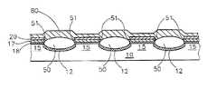
- FIG. 6Billustrates one row of the resultant memory array in side view.
- the polysilicide or polysilicon layer 60lies on top of the ONO structures 16 (FIG. 4), thereby forming the gates 22 (FIG. 1) of the NROM cells.
- Bit line oxides 50are thick enough to isolate neighboring ONO structures 16 .
- the memory chipis then fished in the standard ways, including a side wall oxidation step (typically a self-aligned step), a lightly doped drain (Ldd) implant procedure into the CMOS periphery only and a spacer deposition.
- FIG. 6Aillustrates the location of the spacers 62 as being along the sidewalls of the polysilicon word lines 60 .
- the Lddtypically requires separate masks for the n-channel and p-channel periphery transistors.
- the thicknesses of the various elements of the NROM cellare generally independent of each other.
- the thicknesses of the bottom oxide, nitride and top oxide layersare typically selected as a function of the desired operation of the memory array
- the bit line oxideis independent of the thickness of bottom oxide ONO structure
- tie gate oxide of the peripheryis independent of the other two oxide (i.e., the bit line oxide and the bottom ONO oxide) thicknesses.
Landscapes
- Engineering & Computer Science (AREA)
- Physics & Mathematics (AREA)
- Condensed Matter Physics & Semiconductors (AREA)
- General Physics & Mathematics (AREA)
- Manufacturing & Machinery (AREA)
- Computer Hardware Design (AREA)
- Microelectronics & Electronic Packaging (AREA)
- Power Engineering (AREA)
- Non-Volatile Memory (AREA)
- Semiconductor Memories (AREA)
Abstract
Description
- The present invention relates generally to methods of fabrication of nitride read only memory (NROM) cells and arrays.[0001]
- FIG. 1, to which reference is made, illustrates a typical prior art NROM cell. This cell includes a[0002]
substrate 10 in which are implanted asource 12 and adrain 14 and on top of which lies an oxide-nitride-oxide (ONO)structure 16 having a layer ofnitride 17 sandwiched between twooxide layers ONO structure 16 lies agate conductor 22. Betweensource 12 anddrain 14 is achannel 15 formed underONO structure 16. - Nitride[0003]
section 17 provides the charge retention mechanism for programming the memory cell. Specifically, when programming voltages are provided tosource 12,drain 14 andgate conductor 22, electrons flow towardsdrain 14. According to the hot electron injection phenomenon, some hot electrons penetrate rough the lower section ofsilicon oxide 18, especially ifsection 18 is thin, and are then collected innitride section 17. As is known in the art,nitride section 17 retains the received charge, labeled24, in a concentrated areaadjacent drain 14.Concentrated charge 24 significantly raises the threshold of the portion of the channel of the memory cell undercharge 24 to be higher than the threshold of the remaining portion of thechannel 15. - When[0004]
concentrated charge 24 is present (i.e the cell is programmed), the raised threshold of the cell does not pert the cell to be placed into a conductive state during reading of the cell. Ifconcentrated charge 24 is not present, the read voltage ongate conductor 22 can overcome the much lower threshold and accordingly,channel 15 becomes inverted and hence, conductive. - U.S. application Ser. No. 08/861,430 filed Jul. 23, 1996 and owned by the common inventor of he present invention describes an improved NROM cell, which is programmed in one direction and read in the reverse direction.[0005]
- It is noted that the threshold voltage Vth of NROM cells is generally very sensitive to the voltages Vdrain and Vgate provided on the[0006]
drain 14 and on thegate 22, respectively. Furthermore, U.S. application Ser. No. 08/861,430 selects the voltages Vdrain and Vgate are selected in order to ensure that the charge trapped in a portion of thenitride layer 17 remains localized in that portion. - Read only memory cells, including a nitride layer in the gate dielectric (NROM) are described, inter alia, in U.S. Pat. No. 5,168,334 to Mitchell et al. and U.S. Pat. No. 4,173,766 to Hayes.[0007]
- Mitchell et al. describe two processes to produce the NROM cells. In the first process, bit lines are first created in the substrate, after which the surface is oxidized. Following the oxidation, the ONO layers are added over the entire array. Polysilicon word lines are then deposited in rows over the ONO layers. Unfortunately, when an oxide layer is grown (typically under high temperature), the already present bit lines will diffuse to the side, an undesirable occurrence which limits the extent to which the cell size can be shrunk.[0008]
- In the second process, the ONO layers are formed over the entire array first, on top of which conducive blocks of polysilicon are formed. The bit lines are implanted between the blocks of polysilicon after which the ONO layers are etched away from on top of the bit lines. Planarized oxide is ten deposited between the polysilicon blocks after which polysilicon word lines are deposited. Mitchell et al. utilize a planarized oxide since such can be deposited rather than grown. Mitchell et al. cannot grow an oxide over the bit lines since such an oxidation operation would also grow oxide over the polysilicon blocks and the latter must be left with a very clean surface in order to connect with the polysilicon word lines. Unfortunately, planarized oxide is not a clean oxide nor does it seal around the edges of the ONO sections Furthermore, the plied oxide adds complexity and cost to the process.[0009]
- Hayes et al. describe au NROM cell having only an oxide-nitride (ON) layer. The cells in the array are created by forming layers of oxide, nitride and polysilicon (the latter to produce the gate) one after another and then patterning and etching these layers to form the on cells. The uncapped nitride in each cell does not hold charge well in both the vertical and lateral directions. Due to hole and hot electron conduction within the nitride, the charge to be stored will flow vertically towards the gate coveting it unless the nitride is tick and will flow laterally in the nitride in response to lateral electric fields.[0010]
- It is an object of the present invention to provide a method of fabricating NROM cells and NROM cell arrays with improved data retention.[0011]
- There is therefore provided, in accordance with a preferred embodiment of the present invention, a method of fabricating an oxide-nitride-oxide (ONO) layer in a memory cell to retain charge in the nitride layer. The method includes the steps of forming a bottom oxide layer on a substrate, depositing a nitride layer and oxidizing a top oxide layer, thereby causing oxygen to be introduced into the nitride layer.[0012]
- Alternatively, in accordance with a preferred embodiment of the present invention, the method includes the steps of forming a bottom oxide layer on a substrate, depositing a nitride layer, oxidizing a portion of a top oxide layer thereby causing oxygen to be introduced into the nitride layer aid doting a remaining portion of the top oxide layer, thereby assist in controlling the amount of oxygen introduced into the nitride layer.[0013]
- Further, in accordance with a preferred embodiment of the present invention, the method includes the steps of for a bottom oxide layer on a substrate, depositing a nitride layer, depositing a portion of a top oxide layer and oxidizing a remaining portion of the top oxide layer, thereby can oxygen to be introduced into the nitride layer.[0014]
- There is provided, in accordance with a preferred embodiment of the present invention, a method for improving the charge retention in a nitride layer of a memory chip. The method includes the steps of deposit a nitride layer and introducing oxygen into the nitride layer.[0015]
- Alternatively, in accordance wit a preferred embodiment of the present invention, the method includes the steps of depositing a nitride layer, controlling the thickness of the deposited nitride layer and introducing oxygen into the nitride layer.[0016]
- Further, in accordance with a preferred embodiment of the present invention, the method includes the steps of forming a bottom oxide layer on a substrate, depositing a nitride layer at a thickness approximate to the final thickness after fabrication, depositing a portion of a top oxide layer and oxidizing a remaining portion of the top oxide layer, thereby assisting in controlling the introduction of oxygen into the nitride layer.[0017]
- The present invention will be understood and appreciated more fully from the following detailed description taken in conjunction with the drawings in which:[0018]
- FIG. 1 is a schematic illustration of a prior art NROM memory cell;[0019]
- FIG. 2 is a schematic illustration of the NROM memory chip after an oxide-nitride-oxide layer has been laid down;[0020]
- FIG. 3A is a schematic illustration in top view of a bit line implant mask;[0021]
- FIG. 3B a cross section of a portion of the memory array of the chip of FIG. 2 after the mask of FIG. 3A is laid down and after etching away the exposed portions of the ONO layer leaving part of the bottom oxide layer;[0022]
- FIG. 3C shows the cross section of FIG. 3B after an implant of an impurity to form the bit lines in the memory away portion of the chip of FIG. 3B;[0023]
- FIG. 4 shows in cross section the memory array portion of the chip of FIG. 3C after oxidation of the bit lines;[0024]
- FIG. 5 is a schematic illustration of an ONO protect mask for the memory array and periphery sections of the chip; and[0025]
- FIGS. 6A and 6B are schematic illusions of the memory array portion of the chip of the present invention after a polysilicon or[0026]
polysilicide layer 60 has been laid down, in top and side views, respectively. - Reference is now made to FIGS. 2, 3A,[0027]3B,3C,4,5,6A and6B, which illustrate the NROM fabrication method of the present invention. Similar reference numerals herein refer to similar elements. It is noted that the present invention covers the fabrication of the entire chip, which includes the NROM memory array portion and the complementary metal oxide semiconductor (CMOS) periphery devices.
- In the following discussion, the process of etching a layer, which includes placing photoresist on the layer, placing a mask on the photoresist, etching wherever the mask is not and removing the photoresist, will not be detailed.[0028]
- The method begins with a standard complementary metal oxide semiconductor (CMOS) initial process for preparing the[0029]
substrate 10 including N well formation and field oxide formation. A screen oxide layer is then grown (not shown) onsubstrate 10 after which it is removed, typically with a wet etch thereby to remove any residual nitride at the edge of the field. A typical thickness of the screen oxide layer is 200-400 Å. - [0030]
Substrate 10 is then overlaid with an ONO layer. Abottom oxide layer 30 is grown oversubstrate 10 typically to a thickness of between 50 Å and 150 Å in a low temperature oxidation operation. A typical oxidation temperature is about 800° C. but it can vary between 750-1000° C. A preferred thickness of thebottom oxide layer 30 is 80 Å. - A[0031]
nitride layer 32 is then deposited overbottom oxide layer 30 to a thickness of between 20 Å and 150 Å where a preferred thickness is as thin as possible, such as 10 Å-50 Å. - Applicant notes that a thin layer of the nitride prohibits lateral movement of the charge retained within the nitride, and hence, it is beneficial to control the thickness of[0032]
nitride layer 32. - [0033]
Top oxide 34 is then produced either through oxidation of the nitride (i.e. growing of the oxide), or by deposition or by a combination thereof. It is noted thattop oxide 34 consumes nitride during oxidation, where typically half of the oxide thickness comes from the consumed nitride. Thus, if it is desired to have a top oxide which is 100 Å thick, thenitride layer 32 should be at least 50 Å thicker than the final desired nitride thickness, with this extra nitride being for consumption in the formation of tie top oxide layer. - It is also noted that, during oxidation of top oxide layer, some of the oxygen is introduced into the non-consumed nitride layer.[0034]
- Ultimately, as is described hereinbelow,[0035]
nitride layer 32 is transformed intonitride section 17, which provides the charge retention mechanism for the memory cell. Nitride, particularly due to its structure, traps the electrons, which are introduced intonitride section 17. Oxygen however, is a better insulator than nitride and helps to minimize the lateral movement of electrons innitride layer 32. It is thus an important element for effective retention of the charge. It is therefore noted tat one of the factors effecting the quality of retention ability ofnitride section 17 is the concentration of oxygen withinnitride layer 32. The oxygen concentration is defied as the percentage of oxygen atoms relative to the nitride atoms, irrespective of the type of molecule in which the oxygen atoms are found. The concentration can range from a low of 10% to a high of 80%. - Hence, in order to produce a retention layer, which provides effective charge retention it is recommended to introduce a high percentage of oxygen into the nitride. Nonetheless, if the oxide-nitride composition is too oxygen rich, even though nitride is essentially an oxidation barrier, a run-away situation is produced whereby[0036]
nitride layer 32 absorbs too much oxygen and ceases to act as a barrier for oxygen diffusion. In such an instance, the oxygen introduced into the oxygenrich nitride layer 32 reaches thesilicone oxide layer 18, and become SIO2. - In summary, in order to produce a[0037]
nitride section 17 with maximum retention qualities, it is desirable to makenitride layer 32 as thin as possible, with the maximum oxygen concentration, without inducing a run-away situation. Consequently, it is critical to control the fabrication the ONO structure, and specifically, the manner in which thetop oxide 34 is produced. - The top oxide is typically of a thickness of between 50 Å and 150 Å. Three alternative operations for creating a[0038]
top oxide 34 of 100 Å are described hereinbelow. - The first method involves depositing[0039]
nitride layer 32 of approximately 150-160 Å, growing 120-130 Å oftop oxide 34, (which includes consuming 60-65 Å of nitride layer32) and removing 20-30 Å ofoxide layer 34 during cleaning. Since a large portion ofnitride layer 32 is consumed, it is difficult to control tie amount of oxygen introduced intonitride layer 32. Thus, in order to avoid a possibility of run-away conditions in the nitride layer, it is essential to “leave” a thicker nitride layer. This alternative produces a thicker nitride layer; however it provides for high introduction of oxygen into the nitride and is a simple process to perform. - The second method involves depositing[0040]
nitride layer 32 at a thickness of approximately 60 Å, growing a tin layer of oxide layer34 (approximately 40 Å) while consuming about 20 Å of nitride, depositing 80-90 Å and removing 20-30 Å during cleaning. Since depositing oxide is a quicker process than growing oxide, this alternative is quicker than the first alternative and it offers marginally better control over the amount of oxygen introduced intonitride layer 32. - It is noted that the longer the oxidation process continues the greater the effect on previously produced layers. Therefore, in order diminish the effect on previous layers, it is desirable to create the top oxide layer as quickly as possible.[0041]
- The third method involves depositing[0042]
nitride layer 32 at a thickness close to the preferred final thickness, such as 20 Å, depositing 100-110 Å of oxide, growing 2-5 Å of oxide and removing 20-30 Å of oxide during cleaning. When growing oxide after it has been deposited, the deposited layer acts as a barrier between th growing oxide andnitride layer 32. Hence, the oxygen is introduced slowly intonitride layer 32. This alternative is slower than the previous alternatives; however, it provides a thin nitride layer and a more controlled manner for regulating the introduction of oxygen into the nitride layer. - The process by which the nitride and top oxide layers are generated depends on the ability of the manufacturing facility to control the thickness and composition of the layers of the ONO structure.[0043]
- At this point, the[0044]
entire substrate 10 is covered wit an ONO layer, as shown in FIG. 2. The next step involves depositing a bit line mask40 (typically photoresist42 patterned in a well known manner), whose layout within the memory array portion of the chip is shown in FIG. 3A, to create the bit lines, forming lines of sources and lines of drains. FIG. 3B illustrates a portion of the resultant chip within the memory array portion with thephotoresist 42 patterned. FIG. 3B is a side view (similar to FIG. 2) with thecolumns 42 of the bit line mask in place.Photoresist columns 42 define the areas where the bit lines are not to be implanted (i.e. the locations of the channels15 (FIG. 1)). - Prior to implanting the bit lines, the top oxide and[0045]
nitride layers columns 42. The etch operation is typically a dry etch which might also etch aportion 44 ofbottom oxide layer 30 which is betweencolumns 42, leavingportion 44 with a predetermined thickness, such as 50 Å. The etch operation producesoxide sections nitride section 17 under eachcolumn 42. - After the etch operation,[0046]
bit lines 12 are implanted (FIG. 3C) in the areas betweencolumns 42. A typical implant might be 2-4×10⁻⁵/cm2of Arsenic at 50 Kev. It will be appreciated that this is a self-aligned implant in which the bit lines are self-aligned to the ONO structures. - The[0047]
photoresist layer 42 is then removed and bit line oxides50 (FIG. 4) are then thermally grown over the bit lines12 in an oxidation operation. At the same time, side oxides551, typically of 30 Å, are grown along the sides of nitride layers17 to improve data retention within the nitride layers. The oxidation typically occurs in the range of 800° C. to 950° C. but preferably at the lower side of this range to minimize the diffusion of the bit line impurity while maximizing the thickness of the thermal oxide. This lowers the bit line capacitance. The oxidation temperature also activates the implanted bit line impurities. - Thus the typical oxidation process is a low temperature oxidation of about 800° C. which, on a P− substrate, normally is continued for a time sufficient to grow the equivalent of 100 Å of thermal oxide. On the chip of the present invention, however,[0048]
top oxide sections 20 will not significantly increase in thickness during the bit line oxidation due to the close presence ofnitride sections 18 whileoxide layer 44 over the bit lines12 will increase significantly due to the presence of Arsenic in the bit lines12. The result is that thebit line oxides 50 are typically very thick, such as 500 Å thick thereby lowering the bit line capacitance. - It will be appreciated that the present invention separates the creation of bottom oxide sections[0049]18 (and thus, of the entire ONO structure16) from the creation of
bit line oxides 50.Bottom oxide sections 18 are created over the entire array as part of creating the ONO structures.Bit line oxides 50 are created during the bit line oxidation operation and this oxidation does not significantly affect the oxide layers in the ONO structures. Furthermore,bit line oxides 50 are self-aligned to the ONO structures and, since the oxidation operation is at a relatively low temperature,bit lines 12 do not significantly diffuse intosubstrate 10 during the oxidation operation. - It will flyer be appreciated that the ONO layers have been laid down on the entire chip and thus, are present in the periphery. In accordance with a preferred embodiment of the present invention, the ONO layers can be utilized as thick gate oxides in the portions of the periphery where thicker oxides are needed. Thus, if two gate dielectric thicknesses are required in the periphery, the present invention provides one gate dielectric using the ONO layers and the second, thinner gate dielectric can be produced in a separate gate oxide production step. Furthermore, as shown in FIG. 5, a[0050]
single mask 52 can be utilized to mark both thelocations 54 of the thick gate oxides as well as to protect the memory array (area56) while etching and oxidizing the periphery. - [0051]
Mask 52 can be utilized in one of two alternative ways. In the first embodiment, a threshold level adjustment implant for the peripheral transistors is performed aftermask 52 is laid down and patterned. This provides tie periphery with a threshold level different from that of thememory array area 56. In the second embodiment, the threshold level adjustment implant is performed on the entire chip prior to laying downmask 52. In this embodiment,mask 52 serves only to mark the locations where the ONO layers are to be removed. - Specifically, in the first embodiment, after[0052]
mask 52 is laid down, the threshold voltage level adjustment is performed. This procedure involves implanting boron through the ONO layers into the portions of the periphery of the chip not covered bymask 52. Typically, there are two adjustment steps, one each for the n-channel and p-channel transistors. It will be appreciated that, in accordance with a preferred embodiment of the present invention, the adjustment implant is performed through the ONO layers since they are not yet capped and thus, do not block the implant operation. It will further be appreciated that, for the threshold adjustment procedure, the to-be-removed ONO layers act as a sacrificial oxide (e.g. an oxide grown for an implant operation and immediately thereafter removed). - Following the threshold voltage adjustment procedure, the ONO layers on the unmasked portions of the chip are removed. Initially, a dry oxide etch is utilized to remove[0053]
top oxide 34 andnitride 32 layers after which a wet etch is utilized to removebottom oxide layer 30. Following removal ofmask 52, a gate oxide (not shown) of typically 100-150 Å is thermally grown over the entire chip. Due to the presence of nitride in the memory array. the gate oxide step does not significantly affect the thickness oftop oxide 20. However, this step creates gate oxides for die transistors in the periphery. - It will be appreciated that the gate oxide thickness is thus independent of the thicknesses of the[0054]
bit line oxide 50 andtop oxide 20. - In a second embodiment,[0055]
mask 52 is laid down after the gate and threshold voltage level adjustment procedure is performed. Thus, the memory array portion of the chip also receives threshold level adjustments. Withmask 52 in place, the ONO layers on the unmasked portions of the chip are removed, as described hereinabove. Once again, the ONO layers act as a sacrificial oxide, eliminating the necessity for the additional sacrificial oxide operations. - Finally, following removal of[0056]
mask 52, a gate oxide is grown over the entire array, creating gate oxides in the periphery only. - Following the gate oxide growth step, a polysilicon layer, which will create word lines for the memory array portion and will create gates for the periphery transistors, is laid down over the chip. If desired, a low resistive suicide, as is known in the art, can be deposited over the polysilicon layer in order to reduce its resistivity. This creates a “polysilicide” layer. A typical total thickness of the polysilicide might be 0.3-0.4 μm. As indicated by FIG. 6A, the polysilicide or polysilicon layer is then etched using a mask into[0057]
word lines 60 within the memory array. Typically the word line etch also etches at least thetop oxide 20 and thenitride 17 from between the word lines60. This improves the charge retention of the memory cells by isolating the nitride layers17 of each transistor. - FIG. 6B illustrates one row of the resultant memory array in side view. The polysilicide or[0058]
polysilicon layer 60 lies on top of the ONO structures16 (FIG. 4), thereby forming the gates22 (FIG. 1) of the NROM cells.Bit line oxides 50 are thick enough to isolate neighboringONO structures 16. - The memory chip is then fished in the standard ways, including a side wall oxidation step (typically a self-aligned step), a lightly doped drain (Ldd) implant procedure into the CMOS periphery only and a spacer deposition. FIG. 6A illustrates the location of the[0059]
spacers 62 as being along the sidewalls of the polysilicon word lines60. The Ldd typically requires separate masks for the n-channel and p-channel periphery transistors. - It will be appreciated that, in the present invention, the thicknesses of the various elements of the NROM cell are generally independent of each other. For example, the thicknesses of the bottom oxide, nitride and top oxide layers are typically selected as a function of the desired operation of the memory array, the bit line oxide is independent of the thickness of bottom oxide ONO structure and tie gate oxide of the periphery is independent of the other two oxide (i.e., the bit line oxide and the bottom ONO oxide) thicknesses.[0060]
- It will be appreciated by persons skilled in the art that the present invention is not limited to what has been particularly shown and described hereinabove. Rather the scope of the present invention is defined only by the claims which follow:[0061]
Claims (6)
Priority Applications (4)
| Application Number | Priority Date | Filing Date | Title |
|---|---|---|---|
| US09/966,754US6803279B2 (en) | 1997-06-11 | 2001-10-01 | NROM fabrication method |
| US10/961,398US7943979B2 (en) | 1997-06-11 | 2004-10-12 | NROM fabrication method |
| US11/979,183US8106442B2 (en) | 1997-06-11 | 2007-10-31 | NROM fabrication method |
| US12/005,323US8008709B2 (en) | 1997-06-11 | 2007-12-27 | NROM fabrication method |
Applications Claiming Priority (3)
| Application Number | Priority Date | Filing Date | Title |
|---|---|---|---|
| US08/873,384US5966603A (en) | 1997-06-11 | 1997-06-11 | NROM fabrication method with a periphery portion |
| US09/365,369US6297096B1 (en) | 1997-06-11 | 1999-07-30 | NROM fabrication method |
| US09/966,754US6803279B2 (en) | 1997-06-11 | 2001-10-01 | NROM fabrication method |
Related Parent Applications (1)
| Application Number | Title | Priority Date | Filing Date |
|---|---|---|---|
| US09/365,369ContinuationUS6297096B1 (en) | 1997-06-11 | 1999-07-30 | NROM fabrication method |
Related Child Applications (1)
| Application Number | Title | Priority Date | Filing Date |
|---|---|---|---|
| US10/961,398ContinuationUS7943979B2 (en) | 1997-06-11 | 2004-10-12 | NROM fabrication method |
Publications (2)
| Publication Number | Publication Date |
|---|---|
| US20020052081A1true US20020052081A1 (en) | 2002-05-02 |
| US6803279B2 US6803279B2 (en) | 2004-10-12 |
Family
ID=23438603
Family Applications (5)
| Application Number | Title | Priority Date | Filing Date |
|---|---|---|---|
| US09/365,369Expired - LifetimeUS6297096B1 (en) | 1997-06-11 | 1999-07-30 | NROM fabrication method |
| US09/966,754Expired - LifetimeUS6803279B2 (en) | 1997-06-11 | 2001-10-01 | NROM fabrication method |
| US10/961,398Expired - LifetimeUS7943979B2 (en) | 1997-06-11 | 2004-10-12 | NROM fabrication method |
| US11/979,183Expired - Fee RelatedUS8106442B2 (en) | 1997-06-11 | 2007-10-31 | NROM fabrication method |
| US12/005,323Expired - Fee RelatedUS8008709B2 (en) | 1997-06-11 | 2007-12-27 | NROM fabrication method |
Family Applications Before (1)
| Application Number | Title | Priority Date | Filing Date |
|---|---|---|---|
| US09/365,369Expired - LifetimeUS6297096B1 (en) | 1997-06-11 | 1999-07-30 | NROM fabrication method |
Family Applications After (3)
| Application Number | Title | Priority Date | Filing Date |
|---|---|---|---|
| US10/961,398Expired - LifetimeUS7943979B2 (en) | 1997-06-11 | 2004-10-12 | NROM fabrication method |
| US11/979,183Expired - Fee RelatedUS8106442B2 (en) | 1997-06-11 | 2007-10-31 | NROM fabrication method |
| US12/005,323Expired - Fee RelatedUS8008709B2 (en) | 1997-06-11 | 2007-12-27 | NROM fabrication method |
Country Status (3)
| Country | Link |
|---|---|
| US (5) | US6297096B1 (en) |
| EP (1) | EP1073120A3 (en) |
| JP (1) | JP2001077220A (en) |
Cited By (2)
| Publication number | Priority date | Publication date | Assignee | Title |
|---|---|---|---|---|
| US6482706B1 (en)* | 2001-12-10 | 2002-11-19 | Macronix International Co., Ltd. | Method to scale down device dimension using spacer to confine buried drain implant |
| US20090189214A1 (en)* | 2008-01-30 | 2009-07-30 | Nobuyoshi Takahashi | Semiconductor device and fabrication method for the same |
Families Citing this family (143)
| Publication number | Priority date | Publication date | Assignee | Title |
|---|---|---|---|---|
| US6297096B1 (en)* | 1997-06-11 | 2001-10-02 | Saifun Semiconductors Ltd. | NROM fabrication method |
| IL125604A (en) | 1997-07-30 | 2004-03-28 | Saifun Semiconductors Ltd | Non-volatile electrically erasable and programmble semiconductor memory cell utilizing asymmetrical charge |
| US6768165B1 (en) | 1997-08-01 | 2004-07-27 | Saifun Semiconductors Ltd. | Two bit non-volatile electrically erasable and programmable semiconductor memory cell utilizing asymmetrical charge trapping |
| US6633499B1 (en) | 1997-12-12 | 2003-10-14 | Saifun Semiconductors Ltd. | Method for reducing voltage drops in symmetric array architectures |
| US6633496B2 (en) | 1997-12-12 | 2003-10-14 | Saifun Semiconductors Ltd. | Symmetric architecture for memory cells having widely spread metal bit lines |
| US6430077B1 (en) | 1997-12-12 | 2002-08-06 | Saifun Semiconductors Ltd. | Method for regulating read voltage level at the drain of a cell in a symmetric array |
| US6490204B2 (en) | 2000-05-04 | 2002-12-03 | Saifun Semiconductors Ltd. | Programming and erasing methods for a reference cell of an NROM array |
| US6928001B2 (en) | 2000-12-07 | 2005-08-09 | Saifun Semiconductors Ltd. | Programming and erasing methods for a non-volatile memory cell |
| US6396741B1 (en) | 2000-05-04 | 2002-05-28 | Saifun Semiconductors Ltd. | Programming of nonvolatile memory cells |
| US6614692B2 (en) | 2001-01-18 | 2003-09-02 | Saifun Semiconductors Ltd. | EEPROM array and method for operation thereof |
| US6495475B2 (en)* | 2001-03-28 | 2002-12-17 | Atmel Corporation | Method for fabrication of a high capacitance interpoly dielectric |
| US6677805B2 (en) | 2001-04-05 | 2004-01-13 | Saifun Semiconductors Ltd. | Charge pump stage with body effect minimization |
| US6584017B2 (en) | 2001-04-05 | 2003-06-24 | Saifun Semiconductors Ltd. | Method for programming a reference cell |
| TW480678B (en)* | 2001-04-13 | 2002-03-21 | Macronix Int Co Ltd | Method for producing nitride read only memory (NROM) |
| US6636440B2 (en) | 2001-04-25 | 2003-10-21 | Saifun Semiconductors Ltd. | Method for operation of an EEPROM array, including refresh thereof |
| US6643181B2 (en) | 2001-10-24 | 2003-11-04 | Saifun Semiconductors Ltd. | Method for erasing a memory cell |
| TW503509B (en)* | 2001-10-29 | 2002-09-21 | Macronix Int Co Ltd | Manufacture method of substrate/oxide nitride/oxide/silicon device |
| US6897522B2 (en) | 2001-10-31 | 2005-05-24 | Sandisk Corporation | Multi-state non-volatile integrated circuit memory systems that employ dielectric storage elements |
| US6925007B2 (en) | 2001-10-31 | 2005-08-02 | Sandisk Corporation | Multi-state non-volatile integrated circuit memory systems that employ dielectric storage elements |
| CN100438037C (en)* | 2001-11-07 | 2008-11-26 | 旺宏电子股份有限公司 | Multi-level NROM memory cell and operation method thereof |
| US6514831B1 (en)* | 2001-11-14 | 2003-02-04 | Macronix International Co., Ltd. | Nitride read only memory cell |
| US7098107B2 (en) | 2001-11-19 | 2006-08-29 | Saifun Semiconductor Ltd. | Protective layer in memory device and method therefor |
| US6885585B2 (en) | 2001-12-20 | 2005-04-26 | Saifun Semiconductors Ltd. | NROM NOR array |
| US6800493B2 (en)* | 2001-12-20 | 2004-10-05 | Macronix International Co., Ltd. | Pre-erase manufacturing method |
| US6500713B1 (en) | 2001-12-20 | 2002-12-31 | Advanced Micro Devices, Inc. | Method for repairing damage to charge trapping dielectric layer from bit line implantation |
| US6583007B1 (en) | 2001-12-20 | 2003-06-24 | Saifun Semiconductors Ltd. | Reducing secondary injection effects |
| US7309629B2 (en) | 2002-01-02 | 2007-12-18 | Matsushita Electric Industrial Co., Ltd. | Method for fabricating semiconductor device |
| JP4540993B2 (en) | 2004-01-20 | 2010-09-08 | パナソニック株式会社 | Manufacturing method of semiconductor device |
| US6700818B2 (en) | 2002-01-31 | 2004-03-02 | Saifun Semiconductors Ltd. | Method for operating a memory device |
| TW544866B (en)* | 2002-05-06 | 2003-08-01 | Macronix Int Co Ltd | Fabrication method for a mask read only memory device |
| US6777725B2 (en)* | 2002-06-14 | 2004-08-17 | Ingentix Gmbh & Co. Kg | NROM memory circuit with recessed bitline |
| US6853587B2 (en)* | 2002-06-21 | 2005-02-08 | Micron Technology, Inc. | Vertical NROM having a storage density of 1 bit per 1F2 |
| CN100407427C (en)* | 2002-06-21 | 2008-07-30 | 微米技术股份有限公司 | NROM memory element, memory array, related apparatus and method |
| US6917544B2 (en) | 2002-07-10 | 2005-07-12 | Saifun Semiconductors Ltd. | Multiple use memory chip |
| US6826107B2 (en) | 2002-08-01 | 2004-11-30 | Saifun Semiconductors Ltd. | High voltage insertion in flash memory cards |
| US7136304B2 (en) | 2002-10-29 | 2006-11-14 | Saifun Semiconductor Ltd | Method, system and circuit for programming a non-volatile memory array |
| US6777762B2 (en) | 2002-11-05 | 2004-08-17 | Macronix International Co., Ltd. | Mask ROM structure having a coding layer between gates and word lines |
| DE10259783A1 (en)* | 2002-12-19 | 2004-07-15 | Infineon Technologies Ag | Method for improving process step sequence in forming semiconductor memories with charge trapping memory cells, used same masks as used for forming doped troughs outside memory cell field for removing HV gate dielectric |
| US7178004B2 (en) | 2003-01-31 | 2007-02-13 | Yan Polansky | Memory array programming circuit and a method for using the circuit |
| US6803284B2 (en) | 2003-02-10 | 2004-10-12 | Macronix International Co., Ltd. | Method for manufacturing embedded non-volatile memory with two polysilicon layers |
| US6699757B1 (en) | 2003-03-26 | 2004-03-02 | Macronix International Co., Ltd. | Method for manufacturing embedded non-volatile memory with sacrificial layers |
| US7142464B2 (en) | 2003-04-29 | 2006-11-28 | Saifun Semiconductors Ltd. | Apparatus and methods for multi-level sensing in a memory array |
| US6962728B2 (en)* | 2003-05-16 | 2005-11-08 | Macronix International Co., Ltd. | Method for forming ONO top oxide in NROM structure |
| JP2004356207A (en) | 2003-05-27 | 2004-12-16 | Fujio Masuoka | Semiconductor storage device and method of manufacturing the same |
| DE10324550B4 (en)* | 2003-05-30 | 2006-10-19 | Infineon Technologies Ag | A manufacturing method of an NROM semiconductor memory device |
| US6869843B2 (en)* | 2003-06-27 | 2005-03-22 | Macronix International Co., Ltd. | Non-volatile memory cell with dielectric spacers along sidewalls of a component stack, and method for forming same |
| US7095075B2 (en) | 2003-07-01 | 2006-08-22 | Micron Technology, Inc. | Apparatus and method for split transistor memory having improved endurance |
| US6979857B2 (en) | 2003-07-01 | 2005-12-27 | Micron Technology, Inc. | Apparatus and method for split gate NROM memory |
| US7085170B2 (en)* | 2003-08-07 | 2006-08-01 | Micron Technology, Ind. | Method for erasing an NROM cell |
| US6873550B2 (en)* | 2003-08-07 | 2005-03-29 | Micron Technology, Inc. | Method for programming and erasing an NROM cell |
| US6977412B2 (en) | 2003-09-05 | 2005-12-20 | Micron Technology, Inc. | Trench corner effect bidirectional flash memory cell |
| US7123532B2 (en) | 2003-09-16 | 2006-10-17 | Saifun Semiconductors Ltd. | Operating array cells with matched reference cells |
| US6830963B1 (en)* | 2003-10-09 | 2004-12-14 | Micron Technology, Inc. | Fully depleted silicon-on-insulator CMOS logic |
| US7184315B2 (en)* | 2003-11-04 | 2007-02-27 | Micron Technology, Inc. | NROM flash memory with self-aligned structural charge separation |
| US6869844B1 (en)* | 2003-11-05 | 2005-03-22 | Advanced Micro Device, Inc. | Method and structure for protecting NROM devices from induced charge damage during device fabrication |
| US7202523B2 (en)* | 2003-11-17 | 2007-04-10 | Micron Technology, Inc. | NROM flash memory devices on ultrathin silicon |
| US7183166B2 (en)* | 2003-11-25 | 2007-02-27 | Macronix International Co., Ltd. | Method for forming oxide on ONO structure |
| US7301804B2 (en)* | 2003-12-16 | 2007-11-27 | Micro Technology, Inc. | NROM memory cell, memory array, related devices and methods |
| US7050330B2 (en)* | 2003-12-16 | 2006-05-23 | Micron Technology, Inc. | Multi-state NROM device |
| US7241654B2 (en) | 2003-12-17 | 2007-07-10 | Micron Technology, Inc. | Vertical NROM NAND flash memory array |
| US7157769B2 (en)* | 2003-12-18 | 2007-01-02 | Micron Technology, Inc. | Flash memory having a high-permittivity tunnel dielectric |
| US6937511B2 (en)* | 2004-01-27 | 2005-08-30 | Macronix International Co., Ltd. | Circuit and method for programming charge storage memory cells |
| US7151692B2 (en)* | 2004-01-27 | 2006-12-19 | Macronix International Co., Ltd. | Operation scheme for programming charge trapping non-volatile memory |
| US6878991B1 (en) | 2004-01-30 | 2005-04-12 | Micron Technology, Inc. | Vertical device 4F2 EEPROM memory |
| US7221018B2 (en)* | 2004-02-10 | 2007-05-22 | Micron Technology, Inc. | NROM flash memory with a high-permittivity gate dielectric |
| US6952366B2 (en) | 2004-02-10 | 2005-10-04 | Micron Technology, Inc. | NROM flash memory cell with integrated DRAM |
| US7075146B2 (en) | 2004-02-24 | 2006-07-11 | Micron Technology, Inc. | 4F2 EEPROM NROM memory arrays with vertical devices |
| US7072217B2 (en)* | 2004-02-24 | 2006-07-04 | Micron Technology, Inc. | Multi-state memory cell with asymmetric charge trapping |
| JP2005268418A (en) | 2004-03-17 | 2005-09-29 | Fujio Masuoka | Semiconductor memory device and manufacturing method thereof |
| US7102191B2 (en) | 2004-03-24 | 2006-09-05 | Micron Technologies, Inc. | Memory device with high dielectric constant gate dielectrics and metal floating gates |
| JP2005277183A (en) | 2004-03-25 | 2005-10-06 | Sharp Corp | Nonvolatile semiconductor memory device and manufacturing method thereof |
| US20050215074A1 (en)* | 2004-03-26 | 2005-09-29 | Fuja Shone | ONO formation method |
| US7133313B2 (en)* | 2004-04-26 | 2006-11-07 | Macronix International Co., Ltd. | Operation scheme with charge balancing for charge trapping non-volatile memory |
| US7075828B2 (en)* | 2004-04-26 | 2006-07-11 | Macronix International Co., Intl. | Operation scheme with charge balancing erase for charge trapping non-volatile memory |
| US7187590B2 (en)* | 2004-04-26 | 2007-03-06 | Macronix International Co., Ltd. | Method and system for self-convergent erase in charge trapping memory cells |
| US7164603B2 (en)* | 2004-04-26 | 2007-01-16 | Yen-Hao Shih | Operation scheme with high work function gate and charge balancing for charge trapping non-volatile memory |
| US7209390B2 (en)* | 2004-04-26 | 2007-04-24 | Macronix International Co., Ltd. | Operation scheme for spectrum shift in charge trapping non-volatile memory |
| US7274068B2 (en)* | 2004-05-06 | 2007-09-25 | Micron Technology, Inc. | Ballistic direct injection NROM cell on strained silicon structures |
| US7190614B2 (en)* | 2004-06-17 | 2007-03-13 | Macronix International Co., Ltd. | Operation scheme for programming charge trapping non-volatile memory |
| US20060007732A1 (en)* | 2004-07-06 | 2006-01-12 | Macronix International Co., Ltd. | Charge trapping non-volatile memory and method for operating same |
| US7106625B2 (en)* | 2004-07-06 | 2006-09-12 | Macronix International Co, Td | Charge trapping non-volatile memory with two trapping locations per gate, and method for operating same |
| US7317633B2 (en) | 2004-07-06 | 2008-01-08 | Saifun Semiconductors Ltd | Protection of NROM devices from charge damage |
| US7095655B2 (en) | 2004-08-12 | 2006-08-22 | Saifun Semiconductors Ltd. | Dynamic matching of signal path and reference path for sensing |
| JP4370223B2 (en) | 2004-08-16 | 2009-11-25 | パナソニック株式会社 | Manufacturing method of semiconductor device |
| WO2006035503A1 (en)* | 2004-09-29 | 2006-04-06 | Spansion Llc | Semiconductor device and semiconductor device manufacturing method |
| US7518179B2 (en)* | 2004-10-08 | 2009-04-14 | Freescale Semiconductor, Inc. | Virtual ground memory array and method therefor |
| US7064030B2 (en)* | 2004-10-08 | 2006-06-20 | Freescale Semiconductor, Inc. | Method for forming a multi-bit non-volatile memory device |
| US20060076604A1 (en)* | 2004-10-08 | 2006-04-13 | Prinz Erwin J | Virtual ground memory array and method therefor |
| US7638850B2 (en) | 2004-10-14 | 2009-12-29 | Saifun Semiconductors Ltd. | Non-volatile memory structure and method of fabrication |
| JP2006120719A (en)* | 2004-10-19 | 2006-05-11 | Fujitsu Ltd | Nonvolatile semiconductor memory device and manufacturing method thereof |
| JP4242822B2 (en) | 2004-10-22 | 2009-03-25 | パナソニック株式会社 | Manufacturing method of semiconductor device |
| US7133317B2 (en)* | 2004-11-19 | 2006-11-07 | Macronix International Co., Ltd. | Method and apparatus for programming nonvolatile memory |
| US20060113586A1 (en)* | 2004-11-29 | 2006-06-01 | Macronix International Co., Ltd. | Charge trapping dielectric structure for non-volatile memory |
| US7535765B2 (en) | 2004-12-09 | 2009-05-19 | Saifun Semiconductors Ltd. | Non-volatile memory device and method for reading cells |
| US8482052B2 (en) | 2005-01-03 | 2013-07-09 | Macronix International Co., Ltd. | Silicon on insulator and thin film transistor bandgap engineered split gate memory |
| US7473589B2 (en) | 2005-12-09 | 2009-01-06 | Macronix International Co., Ltd. | Stacked thin film transistor, non-volatile memory devices and methods for fabricating the same |
| US7315474B2 (en) | 2005-01-03 | 2008-01-01 | Macronix International Co., Ltd | Non-volatile memory cells, memory arrays including the same and methods of operating cells and arrays |
| EP1686592A3 (en) | 2005-01-19 | 2007-04-25 | Saifun Semiconductors Ltd. | Partial erase verify |
| US8053812B2 (en) | 2005-03-17 | 2011-11-08 | Spansion Israel Ltd | Contact in planar NROM technology |
| US7158420B2 (en)* | 2005-04-29 | 2007-01-02 | Macronix International Co., Ltd. | Inversion bit line, charge trapping non-volatile memory and method of operating same |
| US20060281255A1 (en)* | 2005-06-14 | 2006-12-14 | Chun-Jen Chiu | Method for forming a sealed storage non-volative multiple-bit memory cell |
| US7763935B2 (en)* | 2005-06-23 | 2010-07-27 | Macronix International Co., Ltd. | ONO formation of semiconductor memory device and method of fabricating the same |
| US7786512B2 (en) | 2005-07-18 | 2010-08-31 | Saifun Semiconductors Ltd. | Dense non-volatile memory array and method of fabrication |
| US7763927B2 (en) | 2005-12-15 | 2010-07-27 | Macronix International Co., Ltd. | Non-volatile memory device having a nitride-oxide dielectric layer |
| US7468299B2 (en)* | 2005-08-04 | 2008-12-23 | Macronix International Co., Ltd. | Non-volatile memory cells and methods of manufacturing the same |
| US7668017B2 (en) | 2005-08-17 | 2010-02-23 | Saifun Semiconductors Ltd. | Method of erasing non-volatile memory cells |
| US7704865B2 (en)* | 2005-08-23 | 2010-04-27 | Macronix International Co., Ltd. | Methods of forming charge-trapping dielectric layers for semiconductor memory devices |
| US7221138B2 (en) | 2005-09-27 | 2007-05-22 | Saifun Semiconductors Ltd | Method and apparatus for measuring charge pump output current |
| US7352627B2 (en) | 2006-01-03 | 2008-04-01 | Saifon Semiconductors Ltd. | Method, system, and circuit for operating a non-volatile memory array |
| US7808818B2 (en) | 2006-01-12 | 2010-10-05 | Saifun Semiconductors Ltd. | Secondary injection for NROM |
| US7760554B2 (en) | 2006-02-21 | 2010-07-20 | Saifun Semiconductors Ltd. | NROM non-volatile memory and mode of operation |
| US7692961B2 (en) | 2006-02-21 | 2010-04-06 | Saifun Semiconductors Ltd. | Method, circuit and device for disturb-control of programming nonvolatile memory cells by hot-hole injection (HHI) and by channel hot-electron (CHE) injection |
| US8253452B2 (en) | 2006-02-21 | 2012-08-28 | Spansion Israel Ltd | Circuit and method for powering up an integrated circuit and an integrated circuit utilizing same |
| US7638835B2 (en) | 2006-02-28 | 2009-12-29 | Saifun Semiconductors Ltd. | Double density NROM with nitride strips (DDNS) |
| US7701779B2 (en) | 2006-04-27 | 2010-04-20 | Sajfun Semiconductors Ltd. | Method for programming a reference cell |
| US7907450B2 (en) | 2006-05-08 | 2011-03-15 | Macronix International Co., Ltd. | Methods and apparatus for implementing bit-by-bit erase of a flash memory device |
| US7582526B2 (en)* | 2006-06-02 | 2009-09-01 | Macronix International Co., Ltd. | Method for manufacturing semiconductor device |
| JP2008053553A (en) | 2006-08-25 | 2008-03-06 | Matsushita Electric Ind Co Ltd | Semiconductor device and manufacturing method thereof |
| US7556999B2 (en)* | 2006-09-12 | 2009-07-07 | Macronix International Co., Ltd. | Method for fabricating non-volatile memory |
| US7605579B2 (en) | 2006-09-18 | 2009-10-20 | Saifun Semiconductors Ltd. | Measuring and controlling current consumption and output current of charge pumps |
| US8772858B2 (en) | 2006-10-11 | 2014-07-08 | Macronix International Co., Ltd. | Vertical channel memory and manufacturing method thereof and operating method using the same |
| US7811890B2 (en) | 2006-10-11 | 2010-10-12 | Macronix International Co., Ltd. | Vertical channel transistor structure and manufacturing method thereof |
| US8642441B1 (en)* | 2006-12-15 | 2014-02-04 | Spansion Llc | Self-aligned STI with single poly for manufacturing a flash memory device |
| US8223540B2 (en) | 2007-02-02 | 2012-07-17 | Macronix International Co., Ltd. | Method and apparatus for double-sided biasing of nonvolatile memory |
| US8643124B2 (en) | 2007-05-25 | 2014-02-04 | Cypress Semiconductor Corporation | Oxide-nitride-oxide stack having multiple oxynitride layers |
| US8940645B2 (en) | 2007-05-25 | 2015-01-27 | Cypress Semiconductor Corporation | Radical oxidation process for fabricating a nonvolatile charge trap memory device |
| US20090179253A1 (en) | 2007-05-25 | 2009-07-16 | Cypress Semiconductor Corporation | Oxide-nitride-oxide stack having multiple oxynitride layers |
| US9299568B2 (en) | 2007-05-25 | 2016-03-29 | Cypress Semiconductor Corporation | SONOS ONO stack scaling |
| US8633537B2 (en) | 2007-05-25 | 2014-01-21 | Cypress Semiconductor Corporation | Memory transistor with multiple charge storing layers and a high work function gate electrode |
| US8614124B2 (en)* | 2007-05-25 | 2013-12-24 | Cypress Semiconductor Corporation | SONOS ONO stack scaling |
| US9449831B2 (en) | 2007-05-25 | 2016-09-20 | Cypress Semiconductor Corporation | Oxide-nitride-oxide stack having multiple oxynitride layers |
| US7737488B2 (en) | 2007-08-09 | 2010-06-15 | Macronix International Co., Ltd. | Blocking dielectric engineered charge trapping memory cell with high speed erase |
| US9431549B2 (en) | 2007-12-12 | 2016-08-30 | Cypress Semiconductor Corporation | Nonvolatile charge trap memory device having a high dielectric constant blocking region |
| US8198671B2 (en)* | 2009-04-22 | 2012-06-12 | Applied Materials, Inc. | Modification of charge trap silicon nitride with oxygen plasma |
| JP2010263119A (en)* | 2009-05-08 | 2010-11-18 | Panasonic Corp | Nonvolatile semiconductor memory device and manufacturing method thereof |
| JP2010267732A (en)* | 2009-05-13 | 2010-11-25 | Panasonic Corp | Method for manufacturing nonvolatile semiconductor memory device |
| US8471328B2 (en) | 2010-07-26 | 2013-06-25 | United Microelectronics Corp. | Non-volatile memory and manufacturing method thereof |
| US9240405B2 (en) | 2011-04-19 | 2016-01-19 | Macronix International Co., Ltd. | Memory with off-chip controller |
| US8685813B2 (en) | 2012-02-15 | 2014-04-01 | Cypress Semiconductor Corporation | Method of integrating a charge-trapping gate stack into a CMOS flow |
| CN104143553A (en)* | 2013-05-07 | 2014-11-12 | 旺宏电子股份有限公司 | Memory device and method of manufacturing the same |
| US8916432B1 (en)* | 2014-01-21 | 2014-12-23 | Cypress Semiconductor Corporation | Methods to integrate SONOS into CMOS flow |
| US9218978B1 (en) | 2015-03-09 | 2015-12-22 | Cypress Semiconductor Corporation | Method of ONO stack formation |
| JP2019102520A (en)* | 2017-11-29 | 2019-06-24 | ルネサスエレクトロニクス株式会社 | Semiconductor device manufacturing method |
Citations (4)
| Publication number | Priority date | Publication date | Assignee | Title |
|---|---|---|---|---|
| US5467308A (en)* | 1994-04-05 | 1995-11-14 | Motorola Inc. | Cross-point eeprom memory array |
| US5661060A (en)* | 1994-12-28 | 1997-08-26 | National Semiconductor Corporation | Method for forming field oxide regions |
| US5751037A (en)* | 1995-07-27 | 1998-05-12 | Sony Corporation | Non-volatile memory cell having dual gate electrodes |
| US5768192A (en)* | 1996-07-23 | 1998-06-16 | Saifun Semiconductors, Ltd. | Non-volatile semiconductor memory cell utilizing asymmetrical charge trapping |
Family Cites Families (65)
| Publication number | Priority date | Publication date | Assignee | Title |
|---|---|---|---|---|
| US596603A (en)* | 1898-01-04 | Butt-adjuster for grain-binders | ||
| US4017888A (en)* | 1975-12-31 | 1977-04-12 | International Business Machines Corporation | Non-volatile metal nitride oxide semiconductor device |
| US4151021A (en)* | 1977-01-26 | 1979-04-24 | Texas Instruments Incorporated | Method of making a high density floating gate electrically programmable ROM |
| US4173766A (en) | 1977-09-16 | 1979-11-06 | Fairchild Camera And Instrument Corporation | Insulated gate field-effect transistor read-only memory cell |
| US4173791A (en)* | 1977-09-16 | 1979-11-06 | Fairchild Camera And Instrument Corporation | Insulated gate field-effect transistor read-only memory array |
| DE2832388C2 (en) | 1978-07-24 | 1986-08-14 | Siemens Ag, 1000 Berlin Und 8000 Muenchen | Process for the production of MNOS and MOS transistors in silicon gate technology on a semiconductor substrate |
| US4360900A (en)* | 1978-11-27 | 1982-11-23 | Texas Instruments Incorporated | Non-volatile semiconductor memory elements |
| DE2923995C2 (en) | 1979-06-13 | 1985-11-07 | Siemens AG, 1000 Berlin und 8000 München | Process for the production of integrated MOS circuits with MOS transistors and MNOS memory transistors in silicon gate technology |
| WO1981000790A1 (en) | 1979-09-13 | 1981-03-19 | Ncr Co | Silicon gate non-volatile memory device |
| DE2947350A1 (en) | 1979-11-23 | 1981-05-27 | Siemens AG, 1000 Berlin und 8000 München | METHOD FOR PRODUCING MNOS STORAGE TRANSISTORS WITH A VERY SHORT CHANNEL LENGTH IN SILICON GATE TECHNOLOGY |
| JPS56120166A (en)* | 1980-02-27 | 1981-09-21 | Hitachi Ltd | Semiconductor ic device and manufacture thereof |
| US4521796A (en)* | 1980-12-11 | 1985-06-04 | General Instrument Corporation | Memory implant profile for improved channel shielding in electrically alterable read only memory semiconductor device |
| US4382827A (en)* | 1981-04-27 | 1983-05-10 | Ncr Corporation | Silicon nitride S/D ion implant mask in CMOS device fabrication |
| US4527257A (en) | 1982-08-25 | 1985-07-02 | Westinghouse Electric Corp. | Common memory gate non-volatile transistor memory |
| US4701776A (en)* | 1983-08-29 | 1987-10-20 | Seeq Technology, Inc. | MOS floating gate memory cell and process for fabricating same |
| US4769340A (en)* | 1983-11-28 | 1988-09-06 | Exel Microelectronics, Inc. | Method for making electrically programmable memory device by doping the floating gate by implant |
| US4754314A (en)* | 1984-01-24 | 1988-06-28 | Texas Instruments Incorporated | Split-level CMOS |
| US4743564A (en)* | 1984-12-28 | 1988-05-10 | Kabushiki Kaisha Toshiba | Method for manufacturing a complementary MOS type semiconductor device |
| US4667217A (en)* | 1985-04-19 | 1987-05-19 | Ncr Corporation | Two bit vertically/horizontally integrated memory cell |
| US4742492A (en)* | 1985-09-27 | 1988-05-03 | Texas Instruments Incorporated | EEPROM memory cell having improved breakdown characteristics and driving circuitry therefor |
| US5172336A (en) | 1987-07-06 | 1992-12-15 | Canon Kabushiki Kaisha | Method of transferring Bloch lines |
| US5168334A (en) | 1987-07-31 | 1992-12-01 | Texas Instruments, Incorporated | Non-volatile semiconductor memory |
| US4870470A (en)* | 1987-10-16 | 1989-09-26 | International Business Machines Corporation | Non-volatile memory cell having Si rich silicon nitride charge trapping layer |
| US5159570A (en) | 1987-12-22 | 1992-10-27 | Texas Instruments Incorporated | Four memory state EEPROM |
| US5172338B1 (en) | 1989-04-13 | 1997-07-08 | Sandisk Corp | Multi-state eeprom read and write circuits and techniques |
| US5104819A (en)* | 1989-08-07 | 1992-04-14 | Intel Corporation | Fabrication of interpoly dielctric for EPROM-related technologies |
| US5268590A (en)* | 1989-12-27 | 1993-12-07 | Motorola, Inc. | CMOS device and process |
| US5226502A (en)* | 1990-03-28 | 1993-07-13 | Mazda Motor Corporation | Differential limiter for vehicle |
| US5266502A (en) | 1990-04-03 | 1993-11-30 | Olympus Optical Co., Ltd. | STM memory medium |
| US5424567A (en)* | 1991-05-15 | 1995-06-13 | North American Philips Corporation | Protected programmable transistor with reduced parasitic capacitances and method of fabrication |
| US5514616A (en)* | 1991-08-26 | 1996-05-07 | Lsi Logic Corporation | Depositing and densifying glass to planarize layers in semi-conductor devices based on CMOS structures |
| JPH0575133A (en)* | 1991-09-11 | 1993-03-26 | Rohm Co Ltd | Non-volatile storage device |
| US5175120A (en) | 1991-10-11 | 1992-12-29 | Micron Technology, Inc. | Method of processing a semiconductor wafer to form an array of nonvolatile memory devices employing floating gate transistors and peripheral area having CMOS transistors |
| JPH05110114A (en)* | 1991-10-17 | 1993-04-30 | Rohm Co Ltd | Nonvolatile semiconductor memory device |
| JP3358663B2 (en) | 1991-10-25 | 2002-12-24 | ローム株式会社 | Semiconductor storage device and storage information reading method thereof |
| US5525534A (en)* | 1992-03-13 | 1996-06-11 | Fujitsu Limited | Method of producing a semiconductor device using a reticle having a polygonal shaped hole |
| US5324675A (en)* | 1992-03-31 | 1994-06-28 | Kawasaki Steel Corporation | Method of producing semiconductor devices of a MONOS type |
| EP0597124B1 (en) | 1992-05-29 | 1998-12-09 | Citizen Watch Co. Ltd. | Method of fabricating a semiconductor nonvolatile storage device |
| GB9217743D0 (en) | 1992-08-19 | 1992-09-30 | Philips Electronics Uk Ltd | A semiconductor memory device |
| US5436481A (en) | 1993-01-21 | 1995-07-25 | Nippon Steel Corporation | MOS-type semiconductor device and method of making the same |
| US5459083A (en)* | 1993-03-01 | 1995-10-17 | Motorola, Inc. | Method for making BIMOS device having a bipolar transistor and a MOS triggering transistor |
| US5477499A (en) | 1993-10-13 | 1995-12-19 | Advanced Micro Devices, Inc. | Memory architecture for a three volt flash EEPROM |
| US5511020A (en)* | 1993-11-23 | 1996-04-23 | Monolithic System Technology, Inc. | Pseudo-nonvolatile memory incorporating data refresh operation |
| JPH07193151A (en) | 1993-12-27 | 1995-07-28 | Toshiba Corp | Nonvolatile semiconductor memory device and its storage method |
| KR100331127B1 (en)* | 1994-02-15 | 2002-10-18 | 내셔널 세미콘덕터 코포레이션 | High Voltage CMOS Transistors for Standard CMOS Processes |
| US5418176A (en)* | 1994-02-17 | 1995-05-23 | United Microelectronics Corporation | Process for producing memory devices having narrow buried N+ lines |
| US5623443A (en)* | 1994-03-11 | 1997-04-22 | Waferscale Integration, Inc. | Scalable EPROM array with thick and thin non-field oxide gate insulators |
| US5619052A (en)* | 1994-09-29 | 1997-04-08 | Macronix International Co., Ltd. | Interpoly dielectric structure in EEPROM device |
| US5633202A (en)* | 1994-09-30 | 1997-05-27 | Intel Corporation | High tensile nitride layer |
| JP3305901B2 (en)* | 1994-12-14 | 2002-07-24 | 東芝マイクロエレクトロニクス株式会社 | Method for manufacturing semiconductor device |
| DE19505293A1 (en) | 1995-02-16 | 1996-08-22 | Siemens Ag | Multi-value read-only memory cell with improved signal-to-noise ratio |
| US5869590A (en)* | 1995-04-12 | 1999-02-09 | Eastman Chemical Company | Waterborne polymers having pendant allyl groups |
| KR100187656B1 (en) | 1995-05-16 | 1999-06-01 | 김주용 | Method for manufacturing a flash eeprom and the programming method |
| DE69528971D1 (en) | 1995-06-30 | 2003-01-09 | St Microelectronics Srl | Method of manufacturing a circuit containing non-volatile memory cells and edge transistors of at least two different types, and corresponding IC |
| US5866458A (en)* | 1995-08-29 | 1999-02-02 | Lg Semicon Co., Ltd. | Method for fabricating a CMOS |
| US5925907A (en)* | 1995-09-29 | 1999-07-20 | Nippon Steel Corporaition | Semiconductor device including transistor with composite gate structure and transistor with single gate structure |
| US6330190B1 (en)* | 1996-05-30 | 2001-12-11 | Hyundai Electronics America | Semiconductor structure for flash memory enabling low operating potentials |
| US5953254A (en)* | 1996-09-09 | 1999-09-14 | Azalea Microelectronics Corp. | Serial flash memory |
| US5926730A (en)* | 1997-02-19 | 1999-07-20 | Micron Technology, Inc. | Conductor layer nitridation |
| JPH10335652A (en)* | 1997-05-30 | 1998-12-18 | Hitachi Ltd | Method for manufacturing semiconductor integrated circuit device |
| US5966603A (en) | 1997-06-11 | 1999-10-12 | Saifun Semiconductors Ltd. | NROM fabrication method with a periphery portion |
| US6297096B1 (en)* | 1997-06-11 | 2001-10-02 | Saifun Semiconductors Ltd. | NROM fabrication method |
| US6614070B1 (en)* | 1998-04-16 | 2003-09-02 | Cypress Semiconductor Corporation | Semiconductor non-volatile memory device having a NAND cell structure |
| US6063666A (en)* | 1998-06-16 | 2000-05-16 | Advanced Micro Devices, Inc. | RTCVD oxide and N2 O anneal for top oxide of ONO film |
| US6346442B1 (en)* | 1999-02-04 | 2002-02-12 | Tower Semiconductor Ltd. | Methods for fabricating a semiconductor chip having CMOS devices and a fieldless array |
- 1999
- 1999-07-30USUS09/365,369patent/US6297096B1/ennot_activeExpired - Lifetime
- 2000
- 2000-07-13EPEP00305940Apatent/EP1073120A3/ennot_activeWithdrawn
- 2000-07-28JPJP2000229200Apatent/JP2001077220A/enactivePending
- 2001
- 2001-10-01USUS09/966,754patent/US6803279B2/ennot_activeExpired - Lifetime
- 2004
- 2004-10-12USUS10/961,398patent/US7943979B2/ennot_activeExpired - Lifetime
- 2007
- 2007-10-31USUS11/979,183patent/US8106442B2/ennot_activeExpired - Fee Related
- 2007-12-27USUS12/005,323patent/US8008709B2/ennot_activeExpired - Fee Related
Patent Citations (4)
| Publication number | Priority date | Publication date | Assignee | Title |
|---|---|---|---|---|
| US5467308A (en)* | 1994-04-05 | 1995-11-14 | Motorola Inc. | Cross-point eeprom memory array |
| US5661060A (en)* | 1994-12-28 | 1997-08-26 | National Semiconductor Corporation | Method for forming field oxide regions |
| US5751037A (en)* | 1995-07-27 | 1998-05-12 | Sony Corporation | Non-volatile memory cell having dual gate electrodes |
| US5768192A (en)* | 1996-07-23 | 1998-06-16 | Saifun Semiconductors, Ltd. | Non-volatile semiconductor memory cell utilizing asymmetrical charge trapping |
Cited By (3)
| Publication number | Priority date | Publication date | Assignee | Title |
|---|---|---|---|---|
| US6482706B1 (en)* | 2001-12-10 | 2002-11-19 | Macronix International Co., Ltd. | Method to scale down device dimension using spacer to confine buried drain implant |
| US20090189214A1 (en)* | 2008-01-30 | 2009-07-30 | Nobuyoshi Takahashi | Semiconductor device and fabrication method for the same |
| US8569824B2 (en) | 2008-01-30 | 2013-10-29 | Panasonic Corporation | Semiconductor device and fabrication method for the same |
Also Published As
| Publication number | Publication date |
|---|---|
| US8106442B2 (en) | 2012-01-31 |
| EP1073120A2 (en) | 2001-01-31 |
| US6803279B2 (en) | 2004-10-12 |
| US20080135911A1 (en) | 2008-06-12 |
| US6297096B1 (en) | 2001-10-02 |
| US20080073702A1 (en) | 2008-03-27 |
| US7943979B2 (en) | 2011-05-17 |
| US8008709B2 (en) | 2011-08-30 |
| JP2001077220A (en) | 2001-03-23 |
| US20080099832A1 (en) | 2008-05-01 |
| EP1073120A3 (en) | 2001-03-07 |
Similar Documents
| Publication | Publication Date | Title |
|---|---|---|
| US6803279B2 (en) | NROM fabrication method | |
| US5966603A (en) | NROM fabrication method with a periphery portion | |
| EP0304896B1 (en) | Non-volatile semiconductor memory device and method of the manufacture thereof | |
| US5350937A (en) | Non-volatile memory device having a floating gate | |
| US5445981A (en) | Method of making shallow trench source EPROM cell | |
| US5168334A (en) | Non-volatile semiconductor memory | |
| US5231299A (en) | Structure and fabrication method for EEPROM memory cell with selective channel implants | |
| US6765259B2 (en) | Non-volatile memory transistor array implementing “H” shaped source/drain regions and method for fabricating same | |
| US5352620A (en) | Method of making semiconductor device with memory cells and peripheral transistors | |
| JP2825585B2 (en) | Semiconductor integrated circuit device and method of manufacturing the same | |
| US5885871A (en) | Method of making EEPROM cell structure | |
| US5637520A (en) | Process for fabricating integrated devices including flash-EEPROM memories and transistors | |
| KR920007789B1 (en) | Semiconductor integrated circuit and manufacturing method | |
| US6121087A (en) | Integrated circuit device with embedded flash memory and method for manufacturing same | |
| EP1506573B1 (en) | Manufacturing method for ultra small thin windows in floating gate transistors | |
| GB2080024A (en) | Semiconductor Device and Method for Fabricating the Same | |
| US6248629B1 (en) | Process for fabricating a flash memory device | |
| US5576232A (en) | Fabrication process for flash memory in which channel lengths are controlled | |
| EP0521690B1 (en) | Non-volatile memory and method of manufacturing the same | |
| JP2987860B2 (en) | Manufacturing method of semiconductor nonvolatile memory | |
| JP2864850B2 (en) | Manufacturing method of nonvolatile semiconductor memory device | |
| JP3198682B2 (en) | Manufacturing method of nonvolatile semiconductor memory device | |
| JPH0685442B2 (en) | Semiconductor integrated circuit device and manufacturing method thereof | |
| JP3501405B2 (en) | Manufacturing method of nonvolatile semiconductor device | |
| US6376306B1 (en) | Method for forming non volatile memory structures on a semiconductor substrate |
Legal Events
| Date | Code | Title | Description |
|---|---|---|---|
| AS | Assignment | Owner name:SAIFUN SEMICONDUCTORS LTD., ISRAEL Free format text:ASSIGNMENT OF ASSIGNORS INTEREST;ASSIGNOR:EITAN, BOAZ;REEL/FRAME:015082/0562 Effective date:20040830 | |
| STCF | Information on status: patent grant | Free format text:PATENTED CASE | |
| FEPP | Fee payment procedure | Free format text:PAYER NUMBER DE-ASSIGNED (ORIGINAL EVENT CODE: RMPN); ENTITY STATUS OF PATENT OWNER: LARGE ENTITY Free format text:PAYOR NUMBER ASSIGNED (ORIGINAL EVENT CODE: ASPN); ENTITY STATUS OF PATENT OWNER: LARGE ENTITY | |
| FPAY | Fee payment | Year of fee payment:4 | |
| FPAY | Fee payment | Year of fee payment:8 | |
| AS | Assignment | Owner name:SPANSION TECHNOLOGY LLC, CALIFORNIA Free format text:TERMINATION AND RELEASE OF SECURITY INTEREST IN PATENT COLLATERAL;ASSIGNOR:BARCLAYS BANK PLC;REEL/FRAME:034715/0305 Effective date:20141227 Owner name:SPANSION LLC, CALIFORNIA Free format text:TERMINATION AND RELEASE OF SECURITY INTEREST IN PATENT COLLATERAL;ASSIGNOR:BARCLAYS BANK PLC;REEL/FRAME:034715/0305 Effective date:20141227 Owner name:SPANSION INC., CALIFORNIA Free format text:TERMINATION AND RELEASE OF SECURITY INTEREST IN PATENT COLLATERAL;ASSIGNOR:BARCLAYS BANK PLC;REEL/FRAME:034715/0305 Effective date:20141227 Owner name:SPANSION TECHNOLOGY INC., CALIFORNIA Free format text:TERMINATION AND RELEASE OF SECURITY INTEREST IN PATENT COLLATERAL;ASSIGNOR:BARCLAYS BANK PLC;REEL/FRAME:034715/0305 Effective date:20141227 | |
| AS | Assignment | Owner name:SPANSION ISRAEL LTD., ISRAEL Free format text:CHANGE OF NAME;ASSIGNOR:SAIFUN SEMICONDUCTORS LTD.;REEL/FRAME:034817/0256 Effective date:20100728 | |
| FPAY | Fee payment | Year of fee payment:12 | |
| AS | Assignment | Owner name:MORGAN STANLEY SENIOR FUNDING, INC., NEW YORK Free format text:SECURITY INTEREST;ASSIGNOR:CYPRESS SEMICONDUCTOR CORPORATION;REEL/FRAME:039676/0237 Effective date:20160805 | |
| AS | Assignment | Owner name:MORGAN STANLEY SENIOR FUNDING, NEW YORK Free format text:CORRECTIVE ASSIGNMENT TO CORRECT THE FOLLOWING NUMBERS 6272046,7277824,7282374,7286384,7299106,7337032,7460920,7519447 PREVIOUSLY RECORDED ON REEL 039676 FRAME 0237. ASSIGNOR(S) HEREBY CONFIRMS THE SECURITY INTEREST;ASSIGNOR:CYPRESS SEMICONDUCTOR CORPORATION;REEL/FRAME:047797/0854 Effective date:20171229 |