US20020050795A1 - Active matrix organic el display device and method of forming the same - Google Patents
Active matrix organic el display device and method of forming the sameDownload PDFInfo
- Publication number
- US20020050795A1 US20020050795A1US09/984,303US98430301AUS2002050795A1US 20020050795 A1US20020050795 A1US 20020050795A1US 98430301 AUS98430301 AUS 98430301AUS 2002050795 A1US2002050795 A1US 2002050795A1
- Authority
- US
- United States
- Prior art keywords
- circuitry
- shielding
- region
- layer
- shielding wall
- Prior art date
- Legal status (The legal status is an assumption and is not a legal conclusion. Google has not performed a legal analysis and makes no representation as to the accuracy of the status listed.)
- Granted
Links
- 239000011159matrix materialSubstances0.000titleclaimsabstractdescription62
- 238000000034methodMethods0.000titleclaimsdescription44
- 238000004020luminiscence typeMethods0.000claimsabstractdescription99
- 230000003287optical effectEffects0.000claimsabstractdescription65
- 238000005401electroluminescenceMethods0.000claimsabstractdescription52
- 239000000758substrateSubstances0.000claimsabstractdescription45
- 230000005684electric fieldEffects0.000claimsabstractdescription16
- 239000010409thin filmSubstances0.000claimsdescription101
- 239000000463materialSubstances0.000claimsdescription45
- 238000000151depositionMethods0.000claimsdescription2
- 239000010410layerSubstances0.000description216
- 239000010408filmSubstances0.000description77
- 239000012212insulatorSubstances0.000description23
- 239000011229interlayerSubstances0.000description23
- 229910021420polycrystalline siliconInorganic materials0.000description23
- 229920005591polysiliconPolymers0.000description23
- 230000004048modificationEffects0.000description17
- 238000012986modificationMethods0.000description17
- 238000001459lithographyMethods0.000description15
- 229910052738indiumInorganic materials0.000description12
- APFVFJFRJDLVQX-UHFFFAOYSA-Nindium atomChemical compound[In]APFVFJFRJDLVQX-UHFFFAOYSA-N0.000description12
- 238000003475laminationMethods0.000description11
- 239000003990capacitorSubstances0.000description10
- 238000005229chemical vapour depositionMethods0.000description10
- 229910021417amorphous siliconInorganic materials0.000description9
- 230000005525hole transportEffects0.000description9
- VYPSYNLAJGMNEJ-UHFFFAOYSA-NSilicium dioxideChemical compoundO=[Si]=OVYPSYNLAJGMNEJ-UHFFFAOYSA-N0.000description8
- 230000002093peripheral effectEffects0.000description8
- 229910052814silicon oxideInorganic materials0.000description8
- 229910052782aluminiumInorganic materials0.000description7
- XAGFODPZIPBFFR-UHFFFAOYSA-NaluminiumChemical compound[Al]XAGFODPZIPBFFR-UHFFFAOYSA-N0.000description7
- AMGQUBHHOARCQH-UHFFFAOYSA-Nindium;oxotinChemical compound[In].[Sn]=OAMGQUBHHOARCQH-UHFFFAOYSA-N0.000description7
- 238000004544sputter depositionMethods0.000description7
- 239000012535impuritySubstances0.000description6
- 238000002347injectionMethods0.000description6
- 239000007924injectionSubstances0.000description6
- 229910052751metalInorganic materials0.000description6
- 239000002184metalSubstances0.000description6
- 239000011368organic materialSubstances0.000description6
- 230000008569processEffects0.000description6
- XOLBLPGZBRYERU-UHFFFAOYSA-Ntin dioxideChemical compoundO=[Sn]=OXOLBLPGZBRYERU-UHFFFAOYSA-N0.000description6
- 230000007257malfunctionEffects0.000description4
- 229910001148Al-Li alloyInorganic materials0.000description3
- 229910000846In alloyInorganic materials0.000description3
- JFBZPFYRPYOZCQ-UHFFFAOYSA-N[Li].[Al]Chemical compound[Li].[Al]JFBZPFYRPYOZCQ-UHFFFAOYSA-N0.000description3
- JHYLKGDXMUDNEO-UHFFFAOYSA-N[Mg].[In]Chemical compound[Mg].[In]JHYLKGDXMUDNEO-UHFFFAOYSA-N0.000description3
- 230000015572biosynthetic processEffects0.000description3
- 238000004040coloringMethods0.000description3
- 230000007423decreaseEffects0.000description3
- 230000002950deficientEffects0.000description3
- 238000005530etchingMethods0.000description3
- 238000010438heat treatmentMethods0.000description3
- 239000001989lithium alloySubstances0.000description3
- 150000002739metalsChemical class0.000description3
- 239000012780transparent materialSubstances0.000description3
- 150000004767nitridesChemical class0.000description2
- 238000006467substitution reactionMethods0.000description2
- 208000031481Pathologic ConstrictionDiseases0.000description1
- 238000007796conventional methodMethods0.000description1
- 230000007547defectEffects0.000description1
- 238000013461designMethods0.000description1
- 238000011161developmentMethods0.000description1
- 230000006872improvementEffects0.000description1
- 230000000644propagated effectEffects0.000description1
- 230000009467reductionEffects0.000description1
- 238000007789sealingMethods0.000description1
Images


Classifications
- H—ELECTRICITY
- H05—ELECTRIC TECHNIQUES NOT OTHERWISE PROVIDED FOR
- H05B—ELECTRIC HEATING; ELECTRIC LIGHT SOURCES NOT OTHERWISE PROVIDED FOR; CIRCUIT ARRANGEMENTS FOR ELECTRIC LIGHT SOURCES, IN GENERAL
- H05B33/00—Electroluminescent light sources
- H—ELECTRICITY
- H10—SEMICONDUCTOR DEVICES; ELECTRIC SOLID-STATE DEVICES NOT OTHERWISE PROVIDED FOR
- H10D—INORGANIC ELECTRIC SEMICONDUCTOR DEVICES
- H10D30/00—Field-effect transistors [FET]
- H10D30/60—Insulated-gate field-effect transistors [IGFET]
- H10D30/67—Thin-film transistors [TFT]
- H10D30/6704—Thin-film transistors [TFT] having supplementary regions or layers in the thin films or in the insulated bulk substrates for controlling properties of the device
- H10D30/6723—Thin-film transistors [TFT] having supplementary regions or layers in the thin films or in the insulated bulk substrates for controlling properties of the device having light shields
- H—ELECTRICITY
- H10—SEMICONDUCTOR DEVICES; ELECTRIC SOLID-STATE DEVICES NOT OTHERWISE PROVIDED FOR
- H10K—ORGANIC ELECTRIC SOLID-STATE DEVICES
- H10K59/00—Integrated devices, or assemblies of multiple devices, comprising at least one organic light-emitting element covered by group H10K50/00
- H10K59/10—OLED displays
- H10K59/12—Active-matrix OLED [AMOLED] displays
- H10K59/126—Shielding, e.g. light-blocking means over the TFTs
- H—ELECTRICITY
- H10—SEMICONDUCTOR DEVICES; ELECTRIC SOLID-STATE DEVICES NOT OTHERWISE PROVIDED FOR
- H10K—ORGANIC ELECTRIC SOLID-STATE DEVICES
- H10K59/00—Integrated devices, or assemblies of multiple devices, comprising at least one organic light-emitting element covered by group H10K50/00
- H10K59/80—Constructional details
- H10K59/8791—Arrangements for improving contrast, e.g. preventing reflection of ambient light
- H—ELECTRICITY
- H10—SEMICONDUCTOR DEVICES; ELECTRIC SOLID-STATE DEVICES NOT OTHERWISE PROVIDED FOR
- H10K—ORGANIC ELECTRIC SOLID-STATE DEVICES
- H10K50/00—Organic light-emitting devices
- H10K50/80—Constructional details
- H10K50/86—Arrangements for improving contrast, e.g. preventing reflection of ambient light
Definitions
- the present inventionrelates to an active matrix organic electroluminescence display device and a method of forming the same, and more particularly to an improvement in a pixel structure of the active matrix organic electroluminescence display device and a method of forming the pixel structure.
- the active matrix organic electroluminescence display devicehas an array of pixels, each of which includes a circuitry region and an electroluminescence region which exhibits a luminescence upon application of an electric filed.
- the circuitry regionmay often include a thin film transistor having a polysilicon layer.
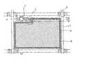
- FIG. 1Ais a fragmentary plan view illustrative of a single pixel structure of the conventional active matrix organic electroluminescence display device.
- FIG. 1Bis a fragmentary cross sectional elevation view illustrative of a single pixel structure of the conventional active matrix organic electroluminescence display device.
- the conventional active matrix organic electroluminescence display deviceexhibits a luminescence upon application of an electric field to a luminescence region 5 .
- the luminescenceis represented by arrow marks.
- the luminescencemay be scattered in a substrate 9 , a gate oxide film 13 , an inter-layer insulator 15 and on interfaces between them.
- the scattered lightis a stray light which may be incident into a polysilicon layer 12 of a thin film transistor.
- the luminescence lightmay be reflected by the substrate 9 so that the reflected light may be a stray light which is incident into the polysilicon layer 12 of the thin film transistor.
- the conventional structure shown in FIG. 1Bhas a planarized insulating layer 25 which may absorb a stray light.
- the luminescenceis, however, omnidirectional.
- a part of the lumincscenceis a light transmitted in a horizontal direction. Such horizontally transmitted light may easily be incident into the polysilicon layer 12 .
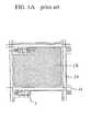
- FIG. 2is a fragmentary cross sectional elevation view of a pixel structure of the conventional active matrix organic electrolumincscence display device, which is disclosed in Japanese laid-open patent publication No. 2000-164875.
- An optical shielding film 26 ais provided under the thin film transistor. This conventional optical shielding structure allows an incident of a stray light in a horizontal direction into the polysilicon layer 12 of the thin film transistor.
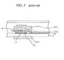
- FIG. 3is a fragmentary cross sectional elevation view of a pixel structure of the conventional active matrix organic electroluminescence display device, which is disclosed in Japanese laid-open patent publication No. 9-80476.
- Top and bottom optical shielding layersare provided over and under the thin film transistor. This conventional optical shielding structure allows an incident of a stray light in a horizontal direction into the polysilicon layer 12 of the thin film transistor.
- the above conventional optical shielding structuresare unable to shield the circuitry such as the thin film transistor from the stray light particularly transmitted in the horizontal direction.
- the present inventionprovides an active matrix organic electroluminescence display device including: a transparent substrate; a plurality of pixels aligned over the transparent substrate, wherein each of the pixels further includes: a luminescent region which exhibits a luminescence upon application of an electric field; a circuitry region including at least a circuitry; and an optical shielding structure provided between the luminescent region and the circuitry region for shielding the circuitry region from the luminescence from the luminescent region.
- FIG. 1Ais a fragmentary plan view illustrative of a single pixel structure of the conventional active matrix organic electroluminescence display device.
- FIG. 1Bis a fragmentary cross sectional elevation view illustrative of a single pixel structure of the conventional active matrix organic electroluminescence display device.
- FIG. 2is a fragmentary cross sectional elevation view of a pixel structure of the conventional active matrix organic electroluminescence display device.
- FIG. 3is a fragmentary cross sectional elevation view of a pixel structure of the conventional active matrix organic electroluminescence display device.
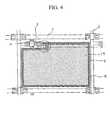
- FIG. 4is a fragmentary plan view of a single pixel of an active matrix organic electroluminescence display device in a first embodiment in accordance with the present invention.
- FIG. 5is a fragmentary enlarged plan view illustrative of a connecting portion between a thin film transistor and an indium tin oxide film in each pixel of FIG. 4.
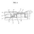
- FIG. 6is a fragmentary cross sectional elevation view illustrative of a single pixel of an active matrix organic electroluminescence display device, taken along an A-A′ line of FIG. 4.
- FIG. 7is a fragmentary enlarged plan view illustrative of a connecting portion between a thin film transistor and an indium tin oxide film in each pixel of an active matrix organic electroluminescence display device in a second embodiment in accordance with the present invention.
- FIG. 8is a fragmentary cross sectional elevation view illustrative of a single pixel of an active matrix organic electroluminescence display device, taken along a B-B′ line of FIG. 7.
- FIG. 9is a fragmentary enlarged plan view illustrative of a connecting portion between a thin film transistor and an indium tin oxide film in each pixel of an active matrix organic electroluminescence display device in a third embodiment in accordance with the present invention.
- FIG 10is a fragmentary cross sectional elevation view illustrative of a single pixel of an active matrix organic electroluminescence display device, taken along a C-C′ line of FIG. 9.
- a first aspect of the present inventionis a pixel structure of an electroluminescence display device.
- the structureincludes: a luminescent region which exhibits a luminescence upon application of an electric field; a circuitry region including at least a circuitry; and an optical shielding structure provided between the luminescent region and the circuitry region for shielding the circuitry region from the luminescence from the luminescent region.
- the optical shielding structureincludes a shielding wall which vertically extends from a lower level than a circuitry of the circuitry region to a higher level than the circuitry.
- the optical shielding structurefurther includes a shielding layer which horizontally extends under the circuitry region.
- the shielding wallvertically extends from a part of an upper surface of the optical shielding structure, and a bottom of the shielding wall is in contact with the part of the upper surface of the optical shielding structure.
- the shielding wallpartially surrounds the luminescent region in a plan view.
- the shielding wallcompletely surrounds the luminescent region in a plan view.
- the shielding wallpartially surrounds the circuitry in a plan view.
- the shielding wallcompletely surrounds the circuitry in a plan view.
- the shielding wallhas a top level which is substantially the same as a wiring layer which is electrically connected to the circuitry.
- the shielding wallhas a top level which is lower than an anode layer of the luminescent region.
- the shielding wallhas a top level which is higher than an anode layer of the luminescent region, and a bottom level which is lower than the anode layer.
- the shielding wallis made of a same material as a wiring layer which is electrically connected to the circuitry.
- the circuitrycomprises a thin film transistor.
- a second aspect of the present inventionis an active matrix organic electroluminescence display device including a transparent substrate; a plurality of pixels aligned over the transparent substrate. Each of the pixels further includes: a luminescent region which exhibits a luminescence upon application of an electric field; a circuitry region including at least a circuitry; and an optical shielding structure provided between the luminescent region and the circuitry region for shielding the circuitry region from the luminescence from the luminescent region.
- the optical shielding strictureincludes a shielding wall which vertically extends from a lower level than a circuitry of the circuitry region to a higher level than the circuitry.
- the optical shielding structurefurther includes a shielding layer which horizontally extends under the circuitry region.
- the shielding wallvertically extends from a part of an upper surface of the optical shielding structure, and a bottom of the shielding wall is in contact with the part of the upper surface of the optical shielding structure.
- the shielding wallpartially surrounds the luminescent region in a plan view.
- the shielding wallcompletely surrounds the luminescent region in a plan view.
- the shielding wallpartially surrounds the circuitry in a plan view.
- the shielding wallcompletely surrounds the circuitry in a plan view.
- the shielding wallhas a top level which is substantially the same as a wing layer which is electrically connected to the circuitry.
- the shielding wallhas a top level which is lower than an anode layer of the luminescent region.
- the shielding wallhas a top level which is higher than an anode layer of the luminescent region, and a bottom level which is lower than the anode layer.
- the shielding wallis made of a same material as a wiring layer which is electrically connected to the circuitry.
- the circuitrycomprises a thin film transistor.
- a third aspect of the present inventionis a method of forming an optical shielding structure between a luminescent region and a circuitry region in a pixel of an electroluminescence display device for shielding the circuitry region from a luminescence from the luminescent region.
- the methodcomprises the stops of: selectively forming an optical shielding layer over a substrate on the circuitry region forming a first insulating layer over the optical shielding layer and the substrate; forming a circuitry over the first insulating layer on the circuitry region; forming a second insulating layer over the circuitry and the first insulating layer; forming at least a first contact hole, which penetrates the second insulating layer and reaches a part of the circuitry, and at least a second contact hole, which penetrates the first and second insulating layers and reaches a part of the optical shielding layer; selectively forming at least a wiring layer electrically connected through the at least first contact hole to the circuitry and also at least an optical shielding wall within the at least second contact hole, wherein the optical shielding wall is in contact with the optical shielding layer.
- the at least second contact holepartially surrounds the luminescent region in a plan view.
- the at least second contact holecompletely surrounds the luminescent region in a plan view.
- the at least second contact holepartially surrounds the circuitry in a plan view.
- the at least second contact holecompletely surrounds the circuitry in a plan view.
- a fourth aspect of the present inventionis a method of forming an optical shielding structure between a luminescent region and a circuitry region in a pixel of an electroluminescence display device for shielding the circuitry region from a luminescence from the luminescent region.
- the methodcomprises the steps of: selectively forming an optical shielding layer over a substrate on the circuitry region; forming a first insulating layer over the optical shielding layer and the substrate; forming a circuitry over the first insulating layer on the circuitry region; forming a second insulating layer over the circuitry and the first insulating layer; forming at least a first contact hole, which penetrates the first and second insulating layers and reaches a part of the optical shielding layer; selectively forming at least an optical shielding wall within the at least first contact hole, wherein the optical shielding wall is in contact with the optical shielding layer; forming a third insulating layer over the at least optical shielding wall and the second insulating layer; forming at least a second contact hole, which penetrates the second and third insulating layer and reaches a part of the circuitry; and selectively forming at least a wiring layer electrically connected through the at least second contact hole to the circuitry.
- the at least first contact holepartially surrounds the luminescent region in a plan view.
- the at least first contact holecompletely surrounds the luminescent region in a plan view.
- the at least first contact holepartially surrounds the circuitry in a plan view.
- the at least first contact holecompletely surrounds the circuitry in a plan view.
- FIG. 4is a fragmentary plan view of a single pixel of an active matrix organic electroluminescence display device in a first embodiment in accordance with the present invention.
- FIG. 5is a fragmentary enlarged plan view illustrative of a connecting portion between a thin film transistor and an indium tin oxide film in each pixel of FIG. 4.
- FIG. 6is a fragmentary cross sectional elevation view illustrative of a single pixel of an active matrix organic electroluminescence display device, taken along an A-A′ line of FIG. 4.
- Each pixelis defined by row wirings 1 and column wirings 2 .
- the pixelincludes a circuit region and an organic EL device 7 .
- the circuit regionincludes a thin film transistor 3 and a capacitor if any.
- a gate electrode 14 of the thin film transistor 3is connected to the row wiring 1 .
- One of source/drain terminals of the thin film transistor 3is connected to the column wiring 2 .
- Another of the source/drain terminals of the thin film transistor 3is connected to an anode 19 of the organic EL device 7 .
- a shielding wall 4is provided along a circumference of a luminescence region 5 , so that the shielding wall 4 encompasses the luminescence region 5 .
- the active matrix organic EL display devicemay be fabricated as follows.
- a transparent substrate 9is prepared.
- a shielding layer made of a shielding material such as WSi or a metal with a thickness of about 200 nanometersis deposited by a sputtering method over the transparent substrate 9 .
- a resist patternis then formed over the shielding layer by use of a lithography technique.
- the shielding layeris then selectively etched by using the resist pattern as a mask, thereby to form a bottom shielding layer 10 over the transparent substrate 9 .
- An insulating film 11such as a silicon oxide film having a thickness of about 600 nanometers is then deposited by a CVD method over the bottom shielding layer 10 and the transparent substrate 9 .
- An amorphous silicon film having a thickness of about 60 nanometersis then deposited by the CVD method over the insulating film 11 .
- An impurityis then doped into the amorphous silicon film.
- a heat treatmentsuch as a laser anneal is then carried out to make the amorphous silicon film into a polysilicon film.
- a resist patternis then formed by a lithography technique over the insulating film 11 .
- the polysilicon filmis selectively etched by using the resist pattern as a mask to form a polysilicon layer 12 over a thin film transistor formation region.
- An insulating film and a WSi film with a thickness of about 200 nanometersare sequentially deposited over the polysilicon layer 12 .
- a resist patternis then formed over the WSi film by a lithography technique.
- the insulating film and the WSi filmare selectively etched by using the resist pattern as a mask, thereby to form a gate insulating film 13 and a gate electrode 14 .
- An impurityis doped into the gate electrode 14 and selected regions of the polysilicon layer 12 .
- a thin film transistor 3is formed over the transparent substrate 9 .
- the drawingillustrates a single thin film transistor. Notwithstanding, it is possible, if any, that a plurality of the thin film transistor 3 and capacitor may also be formed over the transparent substrate 9 .
- An inter-layer insulator 15such as a silicon oxide film with a thickness of about 600 nanometers is deposited by a CVD method over the thin film transistor 3 and the insulating film 11 .
- Source/drain contact holesare formed in the inter-layer insulator 15 , so that the contact holes are positioned in source/drain contact regions.
- a shielding layer contact holeis formed in the inter-layer insulator 15 and the insulating film 11 , so that shielding layer contact hole is positioned over a peripheral region of the bottom shielding layer 10 .
- the shielding layer contact holeextends, in a plan view, to form a trench groove which surrounds the opening of the bottom shielding layer 10 .
- An electrically conductive and optically shielding materialsuch as aluminum is deposited at a thickness of about 500 nanometers by a sputtering method, so that the electrically conductive and optically shielding material is filled within the source/drain contact holes and shielding layer contact holes as well as extends over the inter-layer insulator 15 .
- the electrically conductive and optically shielding material as depositedis in contact with the source and drain of the thin film transistor 3 and connecting portions 8 of the bottom shielding layer 10 .
- a resist patternis formed by a lithography technique over the electrically conductive and optically shielding material.
- the electrically conductive and optically shielding materialis then selectively etched by using the resist pattern as a mask, thereby to form wirings 16 , source and drain contacts 16 a and an optically shielding wall 4 .
- the optically shielding wall 4encompasses the luminescence region 5 .
- the optically shielding wall 4is connected with the connecting portions 8 of the bottom shielding layer 10 , wherein the connecting portions 8 are adjacent to an opening region of the bottom shielding layer 10 .
- the opening region of the bottom shielding layer 10corresponds to the luminescence region 5 .
- the optically shielding wall 4vertically extends and the bottom shielding layer 10 horizontally extends.
- the optically shielding wall 4is provided for isolating the thin film transistor 3 from the luminescence region 5 .
- the optically shielding wall 4is higher than the thin film transistor 3 for shielding the thin film transistor 3 from a stray light which has been transmitted from the organic EL device.
- the bottom shielding layer 10extends under the thin film transistor 3 for shielding the thin film transistor 3 from a stray light which has been reflected at an interface of the transparent substrate 9 .
- the combination of the optically shielding wall 4 with the bottom shielding layer 10forms a three-dimensional optical shielding structure which shields the thin film transistor 3 from any stray lights.
- the optically shielding wall 4is provided along an entirety of the circumference of the luminescence region 5 in order to obtain a high shielding efficiency. It is also possible to modify the optically shielding wall 4 , so that the optically shielding wall 4 partially extends along a stray light significant part of the circumference of the luminescence region 5 .
- a planarized insulating layer 17comprising laminations of an organic film, a silicon oxide film and a nitride film is then deposited over the wirings 16 , the source and drain contacts 16 a and the optically shielding wall 4 as well as over the inter-layer insulator 15 .
- a contact holeis formed in the planarized insulating layer 17 so that the contact hole is positioned over a part of the source and drain contacts 16 a.
- An indium thin oxide film of a thickness of about 150 nanometersis deposited over the planarized insulating layer 17 and also within the contact hole, so that the indium thin oxide film within the contact hole is in contact with the part of the source and drain contacts 16 a .
- a resist patternis formed over the indium thin oxide film by a lithography technique.
- the indium thin oxide filmis selectively etched by using the resist pattern as a mask, thereby forming an anode 19 on a predetermined region.
- the anode 19covers the opening of the bottom shielding layer 10 .
- the anode 19extends on the luminescence region S.
- the anode 19may be made of an electrically conductive and optically transparent material such as indium thin oxide or SnO2.
- a resist layer 18is formed over the planarized insulating layer 17 and a peripheral region of the anode 19 .
- the resist layer 18has, an opening which is positioned inside of the circumference of the anode 19 and also inside of a region defined by the optically shielding wall 4 .
- the opening of the resist layer 18defines the luminescence region 5 .
- the optically shielding wall 4encompasses the opening of the resist layer 18 defining the luminescence region 5 .
- the circumference of the anode 19encompasses the region defined by the optically shielding wall 4 .
- the optically shielding wall 4isolates the luminescence region 5 from the thin film transistor 3 .
- the resist layer 18has a tapered sectioned shape adjacent to the opening, wherein the resist layer 18 gradually decreases in thickness toward the opening.
- a luminescence device layered structure 20is evaporated over the resist layer 18 and over the anode 19 exposed through the opening of the resist layer 18 .
- the luminescence device layered structure 20comprises laminations of a hole injection layer, a hole transport layer, a luminescent layer and an electron transport layer. Those layers are in the range of thickness from 10 nanometers to 50 nanometers.
- the luminescence device layered structure 20comprises laminations of a hole transport layer, a luminescent layer and an electron transport layer.
- the luminescence device layered structure 20comprises laminations of a hole transport layer, a luminescent layer, an electron transport layer and an electron injection layer.
- the luminescence device layered structure 20comprises a single layered structure of a luminescent layer. If a matrix color display is required, the luminescent layer is different in material for respective pixels.
- a cathode 21is evaporated over the luminescence device layered structure 20 .
- the cathode 21may have a thickness of about 200 nanometers.
- Aluminum, magnesium-indium alloy, aluminum-lithium alloyare available for the material of the cathode 21 .
- the pixel of the organic EL display deviceis completed.
- the active matrix organic EL display devicealso includes a power and a peripheral circuit which are not illustrated in the drawings.
- the active matrix organic EL display devicealso includes a scaling structure and a supporting structure which are not illustrated in the drawings.
- the wirings 16 serving as the row wirings 1 and the column wirings 2are provided at a single level, so that the crossing point between the row wirings 1 and the column wirings 2 has a bridge structure which utilizes the WSi layer which has been formed at the same time when the gate electrode has been formed. It is, however, possible as a modification that the row wirings 1 and the column wirings 2 are formed at different levels, wherein the wirings 16 comprise multi-level wirings.
- the luminescence device layered structure 20exhibits a luminescence but only in a region applied with an electric field.
- the resist layer 18prevents the luminescence device layered structure 20 from being applied with the electric field.
- the luminescence device layered structure 20 existing in the opening of the resist layer 18is sandwiched between the anode 19 and the cathode 21 and applied with the electric field.
- the luminescence device layered structure 20existing in the opening of the resist layer 18 , exhibits a luminescence. This luminescence is omnidirectional.
- the optically shielding wall 4is provided for isolating the thin film transistor 3 from the luminescence region 5 .
- the optically shielding wall 4vertically extends from the same level as the bottom shielding layer 10 to the same level as the wirings 16 . Namely, the optically shielding wall 4 vertically extends from a lower level than the bottom of the thin film transistor 3 and a higher level than the top of the thin film transistor 3 . Further, the bottom shielding layer 10 extends under the thin film transistor 3 .
- the combination of the optically shielding wall 4 with the bottom shielding layer 10shields the circuit region including the thin film transistor 3 from any stray lights which have been scattered in the substrate 9 , the insulating layer 11 and the inter-layer insulator 15 ; or reflected by interfaces between them or reflected from the substrate 9 .
- the circuit including the thin film transistor 3is free from any malfunction due to the stray light.
- the active matrix organic EL deviceis free from any defective display.
- the optically shielding wall 4is provided along the entirety of the circumference of the luminescence region 5 in order to obtain a high shielding efficiency. It is also possible to modify the optically shielding wall 4 , so that the optically shielding wall 4 partially extends along a stray light significant part of the circumference of the luminescence region 5 .
- the optically shielding wall 4is aligned to the circumferential line 6 of the anode 19 in consideration of a margin for exposure process, so that the circumferential line 6 of the anode 19 is not out of the optically shielding wall 4 , and also a possible larger area of the luminescence region 5 is ensured.
- the relation in position between the optically shielding wall 4 and the circumferential line 6 of the anode 19may, however, be optional.
- the optically shielding wall 4is formed at the same process for forming the source and drain contacts 16 a and the wirings 16 , provided that the optically shielding wall 4 is made of the same material as the source and drain contacts 16 a and the wirings 16 . No additional process is needed for forming the optically shielding wall 4 .
- the optically shielding wall 4is made of a different optically shielding material from the source and drain contacts 16 a and the wirings 16 .
- Metals or organic materials having optically shielding functionsmay be available for the optically shielding wall 4 .
- Organic materials containing coloring materialsare available.
- the sectional shape of the optically shielding wall 4is illustrated as becoming narrower downwardly because the shielding layer contact hole is slightly tapered downwardly due to etching conditions.
- the tapered sectional shape of the optically shielding wall 4is thus optional, provided that the narrowest portion of the optically shielding wall 4 is sufficient for shielding the stray light.
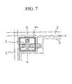
- FIG. 7is a fragmentary enlarged plan view illustrative of a connecting portion between a thin film transistor and an indium tin oxide film in each pixel of an active matrix organic electroluminescence display device in a second embodiment in accordance with the present invention.
- FIG. 8is a fragmentary cross sectional elevation view illustrative of a single pixel of an active matrix organic electroluminescence display device, taken along a B-B′ line of FIG. 7.
- Each pixelis defined by row wirings 1 and column wirings 2 .
- the pixelincludes a circuit region and an organic EL device 7 .
- the circuit regionincludes a thin film transistor 3 and a capacitor if any.
- a gate electrode 14 of the thin film transistor 3is connected to the row wiring 1 .
- One of source/drain terminals of the thin film transistor 3is connected to the column wiring 2 .
- Another of the source/drain terminals of the thin film transistor 3is connected to an anode 19 of the organic EL device 7 .
- a shielding wall 4is provided around a thin film transistor 3 , so that the shielding wall 4 encompasses the circuit region.
- the active matrix organic EL display devicemay be fabricated as follows.
- a transparent substrate 9is prepared.
- a shielding layer made of a shielding material such as WSi or a metal with a thickness of about 200 nanometersis deposited by a sputtering method over the transparent substrate 9 .
- a resist patternis then formed over the shielding layer by use of a lithography technique.
- the shielding layeris then selectively etched by using the resist pattern as a mask, thereby to form a bottom shielding layer 10 over the transparent substrate 9 .
- An insulating film 11such as a silicon oxide film having a thickness of about 600 nanometers is then deposited by a CVD method over the bottom shielding layer 10 and the transparent substrate 9 .
- An amorphous silicon film having a thickness of about 60 nanometersis then deposited by the CVD method over the insulating film 11 .
- An impurityis then doped into the amorphous silicon film.
- a heat treatmentsuch as a laser anneal is then carried out to make the amorphous silicon film into a polysilicon film.
- a resist patternis then formed by a lithography technique over the insulating film 11 .
- the polysilicon filmis selectively etched by using the resist pattern as a mask to form a polysilicon layer 12 over a thin film transistor formation region.
- An insulating film and a WSi film with a thickness of about 200 nanometersare sequentially deposited over the polysilicon layer 12 .
- a resist patternis then formed over the WSi film by a lithography technique.
- the insulating film and the WSi filmare selectively etched by using the resist pattern as a mask, thereby to form a gate insulating film 13 and a gate electrode 14 .
- An impurityis doped into the gate electrode 14 .
- a thin film transistor 3is formed over the transparent substrate 9 .
- the drawingillustrates a single thin film transistor. Notwithstanding, it is possible, if any, that a plurality of the thin film transistor 3 and capacitor may also he formed over the transparent substrate 9 .
- An inter-layer insulator 15such as a silicon oxide film is deposited by a CVD method over the thin film transistor 3 and the insulating film 11 .
- a shielding layer contact holeis formed in the inter-layer insulator 15 and the insulating film 11 , so that shielding layer contact hole is positioned over the bottom shielding layer 10 .
- the shielding layer contact holeextends, in a plan view, to form a square shaped trench groove which surrounds the thin film transistor 3 .
- An electrically conductive and optically shielding material such as aluminumis deposited by a sputtering method, so that the electrically conductive and optically shielding material is filled within the shielding layer contact hole as well as extends over the inter-layer insulator 15 .
- the electrically conductive and optically shielding material as depositedis in contact with connecting portions 8 of the bottom shielding layer 10 .
- a resist patternis formed by a lithography technique over the electrically conductive and optically shielding material.
- the electrically conductive and optically shielding materialis then selectively etched by using the resist pattern as a mask, thereby to form an optically shielding wall 4 .
- the optically shielding wall 4encompasses the thin film transistor 3 .
- the optically shielding wall 4is connected with the connecting portions 8 of the bottom shielding layer 10 , wherein the connecting portions 8 are around the thin film transistor in a plan view.
- the optically shielding wall 4vertically extends and the bottom shielding layer 10 horizontally extends.
- the optically shielding wall 4is provided for isolating the thin film transistor 3 from the luminescence region 5 .
- the optically shielding wall 4is higher than the thin film transistor 3 for shielding the thin film transistor 3 from a stray light which has been transmitted from the organic EL device.
- the bottom shielding layer 10extends under the thin film transistor 3 for shielding the thin film transistor 3 from a stray light which has been reflected at an interface of the transparent substrate 9 .
- the combination of the optically shielding wall 4 with the bottom shielding layer 10forms a three-dimensional optical shielding structure which shields the thin film transistor 3 from any stray lights.
- the optically shielding wall 4is provided along an entirety of the circumference of the thin film transistor 3 in order to obtain a high shielding efficiency. It is also possible to modify the optically shielding wall 4 , so that the optically shielding wall 4 partially extends along a stray light significant part of the circumference of the thin film transistor 3 .
- An additional inter-layer insulator 15 ais also deposited by a CVD method over the inter-layer insulator 15 and the top of the optically shielding wall 4 .
- Contact holesare formed in the additional inter-layer insulator 15 a and the inter-layer insulator 15 .
- a wiring materialsuch as aluminum is deposited by a sputtering method so that the wiring material fills the contact holes and extends over the additional inter-layer insulator 15 a .
- a resist patternis formed by using a lithography technique over the deposited wiring material. The deposited wiring material is selectively etched by using the resist pattern as a mask to form wirings 16 .
- a planarized insulating layer 17comprising laminations of an organic film, a silicon oxide film and a nitride film is then deposited over the wirings 16 and the optically shielding wall 4 as well as over the additional inter-layer insulator 15 a .
- a contact holeis formed in the planarized insulating layer 17 so that the contact hole is positioned over a part of the source and drain contacts.
- An indium thin oxide film of a thickness of about 150 nanometersis deposited over the planarized insulating layer 17 and also within the contact hole, so that the indium thin oxide film within the contact hole is in contact with the part of the source and drain contacts.
- a resist patteris formed over the indium thin oxide film by a lithography technique.
- the indium thin oxide filmis selectively etched by using the resist pattern as a mask, thereby forming an anode 19 on a predetermined region.
- the anode 19covers the opening of the bottom shielding layer 10 .
- the anode 19extends on the luminescence region 5 .
- the anode 19may be made of an electrically conductive and optically transparent material such as indium thin oxide or SnO2.
- a resist layer 18is formed over the planarized insulating layer 17 and a peripheral region of the anode 19 .
- the resist layer 18has an opening which is positioned inside of the circumference of the anode 19 and also inside of a region defined by the optically shielding wall 4 .
- the opening of the resist layer 18defines the luminescence region 5 .
- the optically shielding wall 4encompasses the opening of the resist layer 18 defining the luminescence region 5 .
- the circumference of the anode 19encompasses the region defined by the optically shielding wall 4 .
- the optically shielding wall 4isolates the luminescence region 5 from the thin film transistor 3 .
- the resist layer 18has a tapered sectioned shape adjacent to the opening, wherein the resist layer 18 gradually decreases in thickness toward the opening.
- a luminescence device layered structure 20is evaporated over the resist layer 18 and over the anode 19 exposed through the opening of the resist layer 18 .
- the luminescence device layered structure 20comprises laminations of a hole injection layer, a hole transport layer, a luminescent layer and an electron transport layer. Those layers are in the range of thickness from 10 nanometers to 50 nanometers.
- the luminescence device layered structure 20comprises laminations of a hole transport layer, a luminescent layer and an electron transport layer.
- the luminescence device layered structure 20comprises laminations of a hole transport layer, a luminescent layer, an electron transport layer and an electron injection layer.
- the luminescence device layered structure 20comprises a single layered structure of a luminescent layer. If a matrix color display is required, the luminescent layer is different in material for respective pixels.
- a cathode 21is evaporated over the luminescence device layered structure 20 .
- the cathode 21may have a thickness of about 200 nanometers.
- Aluminum, magnesium-indium alloy, aluminum-lithium alloyare available for the material of the cathode 21 .
- the pixel of the organic EL display deviceis completed.
- the active matrix organic EL display devicealso includes a power and a peripheral circuit which are not illustrated in the drawings.
- the active matrix organic EL display devicealso includes a sealing structure and a supporting structure which are not illustrated in the drawings.
- the wirings 16 serving as the row wirings 1 and the column wirings 2are provided at a single level, so that the crossing point between the row wirings 1 and the column wirings 2 has a bridge structure which utilizes the WSi layer which has been formed at the same time when the gate electrode has been formed. It is, however, possible as a modification that the row wirings 1 and the column wirings 2 are formed at different levels, wherein the wirings 16 comprise multi-level wirings.
- the luminescence device layered structure 20exhibits a luminescence but only in a region applied with an electric field.
- the resist layer 18prevents the luminescence device layered structure 20 from being applied with the electric field.
- the luminescence device layered structure 20 existing in the opening of the resist layer 18is sandwiched between the anode 19 and the cathode 21 and applied with the electric field.
- the luminescence device layered structure 20existing in the opening of the resist layer 18 , exhibits a luminescence. This luminescence is omnidirectional.
- the optically shielding wall 4is provided for isolating the thin film transistor 3 from the luminescence region 5 .
- the optically shielding wall 4vertically extends from the same level as the bottom shielding layer 10 to a higher level than the top of the thin film transistor 3 . Namely, the optically shielding wall 4 vertically extends from a lower level than the bottom of the thin film transistor 3 and a higher level than the top of the thin film transistor 3 . Further, the bottom shielding layer 10 extends under the thin film transistor 3 .
- the combination of the optically shielding wall 4 with the bottom shielding layer 10shields the circuit region including the thin film transistor 3 from any stray lights which have been scattered in the substrate 9 , the insulating layer 11 and the inter-layer insulator 15 or reflected by interfaces between them or reflected from the substrate 9 .
- the circuit including the thin film transistor 3is free from any malfunction due to the stray light.
- the active matrix organic EL deviceis free from any defective display.
- the optically shielding wall 4is provided along the circumference of the thin film transistor 3 in order to obtain a high shielding efficiency. It is also possible to modify the optically shielding wall 4 , so that the optically shielding wall 4 partially extends along a stray light significant part of the circumference of the thin film transistor 3 .
- the optically shielding wall 4is made of a different optically shielding material from the source and drain contacts 16 a and the wirings 16 .
- Metals or organic materials having optically shielding functionsmay be available for the optically shielding wall 4 .
- Organic materials containing coloring materialsare available.
- the sectional shape of the optically shielding wall 4is illustrated as becoming narrower downwardly because the shielding layer contact holes are slightly tapered downwardly due to etching conditions.
- the tapered sectional shape of the optically shielding wall 4is thus optional, provided that the narrowest portion of the optically shielding wall 4 is sufficient for shielding the stray light.
- optically shielding wall 4it is also possible to modify the optically shielding wall 4 , so that the optically shielding wall 4 is provided along the circumference of the thin film transistor 3 except for the wiring 16 , so that the top of the optically shielding wall 4 lies the same level as the wiring 16 , and the optically shielding wall 4 may be formed at the same process for forming the gate contact and the wiring 16 .
- the above structureis suitable for ensuring a larger ratio in area of a luminescence region to a pixel region as compared to the first embodiment.
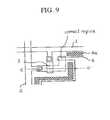
- FIG. 9is a fragmentary enlarged plan view illustrative of a connecting portion between a thin film transistor and an indium tin oxide film in each pixel of an active matrix organic electroluminescence display device in a third embodiment in accordance with the present invention.
- FIG. 10is a fragmentary cross sectional elevation view illustrative of a single pixel of an active matrix organic electroluminescence display device, taken along a C-C′ line of FIG. 9.
- Each pixelis defined by row wirings 1 and column wirings 2 .
- the pixelincludes a circuit region and an organic EL device 7 .
- the circuit regionincludes a thin film transistor 3 and a capacitor if any.
- a gate electrode 14 of the thin film transistor 3is connected to the row wiring 1 .
- One of source/drain terminals of the thin film transistor 3is connected to the column wiring 2 .
- Another of the source/drain terminals of the thin film transistor 3is connected lo an anode 19 of the organic EL device 7 .
- a shielding wall 4is provided along a circumference of a luminescence region 5 , so that the shielding wall 4 encompasses the luminescence region 5 , and the shielding wall 4 also surrounds the anode 19 .
- the top level of the shielding wall 4is higher than the anode 19 and the luminescence region 5 .
- the active matrix organic EL display devicemay be fabricated as follows.
- a transparent substrate 9is prepared.
- a shielding layer made of a shielding material such as WSi or a metal with a thickness of about 200 nanometersis deposited by a sputtering method over the transparent substrate 9 .
- a resist patternis then formed over the shielding layer by use of a lithography technique.
- the shielding layeris then selectively etched by using the resist pattern as a mask, thereby to form a bottom shielding layer 10 over the transparent substrate 9 .
- An insulating film 11such as a silicon oxide film having a thickness of about 600 nanometers is then deposited by a CVD method over the bottom shielding layer 10 and the transparent substrate 9 .
- An amorphous silicon film having a thickness of about 60 nanometersis then deposited by the CVD method over the insulating film 11 .
- An impurityis then doped into the amorphous silicon film.
- a heat treatmentsuch as a laser anneal is then carried out to make the amorphous silicon film into a polysilicon film.
- a resist patternis then formed by a lithography technique over the insulating film 11 .
- the polysilicon filmis selectively etched by using the resist pattern as a mask to form a polysilicon layer 12 over a thin film transistor formation region.
- An insulating film and a WSi film with a thickness of about 200 nanometersare sequentially deposited over the polysilicon layer 12 .
- a resist patternis then formed over the WSi film by a lithography technique.
- the insulating film and the WSi filmare selectively etched by using the resist pattern as a mask, thereby to form a gate insulating film 13 and a gate electrode 14 .
- An impurityis doped into the gate electrode 14 and selected regions of the polysilicon layer 12 .
- a thin film transistor 3is formed over the transparent substrate 9 .
- the drawingillustrates a single thin film transistor. Notwithstanding, it is possible, if any, that a plurality of the thin film transistor 3 and capacitor may also be formed over the transparent substrate 9 .
- An anode 19 of an indium thin oxide filmis selectively formed over the insulating layer 11 , so that a part of the anode 19 is in contact with a part of the polysilicon layer 12 .
- the anode 19covers the opening of the bottom shielding layer 10 .
- the anode 19extends on the luminescence region 5 .
- the anode 19may be made of an electrically conductive and optically transparent material such as indium thin oxide or SnO2.
- the anode 19 and the polysilicon layer 12overly the insulating layer 11 .
- An inter-layer insulator 15such as a silicon oxide film is deposited by a CVD method over the thin film transistor 3 and the insulating film 11 as well as a part of the anode 19 .
- Source/drain contact holesare formed in the inter-layer insulator 15 , so that the contact holes are positioned in source/drain contact regions.
- a shielding layer contact holeis formed in the inter-layer insulator 15 and the insulating film 11 , so that shielding layer contact hole is positioned over a peripheral region of the bottom shielding layer 10 .
- the shielding layer contact holeextends, in a plan view, to form a trench groove which surrounds the opening of the bottom shielding layer 10 .
- An electrically conductive and optically shielding materialsuch as aluminum is deposited by a sputtering method, so that the electrically conductive and optically shielding material is filled within the source/drain contact holes and shielding layer contact holes as well as extends over the inter-layer insulator 15 .
- the electrically conductive and optically shielding material as depositedis in contact with the source and drain of the thin film transistor 3 and connecting portions 8 of the bottom shielding layer 10 .
- a resist patternis formed by a lithography technique over the electrically conductive and optically shielding material.
- the electrically conductive and optically shielding materialis then selectively etched by using the resist pattern as a mask, thereby to form wirings 16 , source and drain contacts 16 a and an optically shielding wall 4 .
- the optically shielding wall 4encompasses the anode 19 .
- the optically shielding wall 4is connected with the connecting portions 8 of the bottom shielding layer 10 , wherein the connecting portions 8 are adjacent to an opening region of the bottom shielding layer 10 .
- the opening region of the bottom shielding layer 10encompasses the luminescence region 5 .
- the optically shielding wall 4vertically extends and the bottom shielding layer 10 horizontally extends.
- the optically shielding wall 4is provided for isolating the thin film transistor 3 from the luminescence region 5 .
- the optically shielding wall 4vertically extends from a lower level than the thin film transistor 3 and the anode 19 to a higher level than the thin film transistor 3 and the anode 19 for shielding the thin film transistor 3 from a stray light which has been propagated through the anode 19 made of indium tin oxide.
- the bottom shielding layer 10extends under the thin film transistor 3 for shielding the thin film transistor 3 from a stray light which has been reflected at an interface of the transparent substrate 9 .
- the combination of the optically shielding wall 4 with the bottom shielding layer 10forms a three-dimensional optical shielding structure which shields the thin film transistor 3 from any stray lights.
- the optically shielding wall 4is provided along an entirety of the circumference of the luminescence region 5 in order to obtain a high shielding efficiency, It is also possible to modify the optically shielding wall 4 , so that the optically shielding wall 4 partially extend, along a stray light significant part of the circumference of the luminescence region 5 .
- a resist layer 18is formed over the inter-layer insulator 15 and a peripheral region of the anode 19 .
- the resist layer 18has art opening which is positioned inside of the circumference of the anode 19 and also inside of a region defined by the optically shielding wall 4 .
- the opening of the resist layer 18defines the luminescence region 5 .
- the optically shielding wall 4encompasses the opening of the resist layer 18 defining the luminescence region 5 .
- the region defined by the optically shielding wall 4encompasses the circumference of the anode 19 .
- the optically shielding wall 4isolates the luminescence region 5 from the thin film transistor 3 .
- the resist layer 18has a tapered sectioned shape adjacent to the opening, wherein the resist layer 18 gradually decreases in thickness toward the opening.
- a luminescence device layered structure 20is evaporated over the resist layer 18 and over the anode 19 exposed through the opening of the resist layer 18 .
- the luminescence device layered structure 20comprises laminations of a hole injection layer, a hole transport layer, a luminescent layer and an electron transport layer. Those layers are in the range of thickness from 10 nanometers to 50 nanometers.
- the luminescence device layered structure 20comprises laminations of a hole transport layer, a luminescent layer and an electron transport layer.
- the luminescence device layered structure 20comprises laminations of a hole transport layer, a luminescent layer, an electron transport layer and an electron injection layer.
- the luminescence device layered structure 20comprises a single layered structure of a luminescent layer. If a matrix color display is required, the luminescent layer is different in material for respective pixels.
- a cathode 21is evaporated over the luminescence device layered structure 20 .
- the cathode 21may have a thickness of about 200 nanometers.
- Aluminum, magnesium-indium alloy, aluminum-lithium alloyare available for the material of the cathode 21 .
- the pixel of the organic EL display deviceis completed.
- the active matrix organic EL display devicealso includes a power and a peripheral circuit which are not illustrated in the drawings.
- the active matrix organic EL display devicealso includes a scaling structure and a supporting structure which are not illustrated in the drawings.
- the wirings 16 serving as the row wirings 1 and the column wirings 2are provided at a single level, so that the crossing point between the row wirings 1 and the column wirings 2 has a bridge structure which utilizes the WSi layer which has been formed at the same time when the gate electrode has been formed. It is, however, possible as a modification that the row wirings 1 and the column wirings 2 are formed at different levels, wherein the wirings 16 comprise multi-level wirings.
- the luminescence device layered structure 20exhibits a luminescence but only in a region applied with an electric field.
- the resist layer 18prevents the luminescence device layered structure 20 from being applied with the electric field.
- the luminescence device layered structure 20 existing in the opening of the resist layer 18is sandwiched between the anode 19 and the cathode 21 and applied with the electric field.
- the luminescence device layered structure 20existing in the opening of the resist layer 18 , exhibits a luminescence. This luminescence is omnidirectional.
- the optically shielding wall 4is provided for isolating the thin film transistor 3 from the luminescence region 5 .
- the optically shielding wall 4vertically extends from the same level as the bottom shielding layer 10 to the same level as the wirings 16 . Namely, the optically shielding wall 4 vertically extends from a lower level than the bottom of the thin film transistor 3 and a higher level than the top of the thin film transistor 3 . Further, the bottom shielding layer 10 extends under the thin film transistor 3 .
- the combination of the optically shielding wall 4 with the bottom shielding layer 10shields the circuit region including the thin film transistor 3 from any stray lights which have been scattered in the substrate 9 , the insulating layer 11 and the inter-layer insulator 15 or reflected by interfaces between them or reflected from the substrate 9 .
- the circuit including the thin film transistor 3is free from any malfunction due to the stray light.
- the active matrix organic ET, deviceis free from any defective display.
- the optically shielding wall 4is provided along the entirety of the circumference of the luminescence region 5 in order to obtain a high shielding efficiency. It is also possible to modify the optically shielding wall 4 , so that the optically shielding wall 4 partially extends along a stray light significant part of the circumference of the luminescence region 5 .
- the optically shielding wall 4is formed at the same process for forming the source and drain contacts 16 a and the wirings 16 , provided that the optically shielding wall 4 is made of the same material as the source and drain contacts 16 a and the wirings 16 . No additional process is needed for forming the optically shielding wall 4 .
- the optically shielding wall 4is made of a different optically shielding material from the source and drain contacts 16 a and the wirings 16 .
- Metals or organic materials having optically shielding functionsmay be available for the optically shielding wall 4 .
- Organic materials containing coloring materialsare available.
- the sectional shape of the optically shielding wall 4is illustrated as becoming narrower downwardly because the shielding layer contact hole is slightly tapered downwardly due to etching conditions.
- the tapered sectional shape of the optically shielding wall 4is thus optional, provided that the narrowest portion of the optically shielding wall 4 is sufficient for shielding the stray light.
Landscapes
- Engineering & Computer Science (AREA)
- Microelectronics & Electronic Packaging (AREA)
- Electroluminescent Light Sources (AREA)
- Devices For Indicating Variable Information By Combining Individual Elements (AREA)
- Thin Film Transistor (AREA)
Abstract
Description
- 1. Field of the Invention[0001]
- The present invention relates to an active matrix organic electroluminescence display device and a method of forming the same, and more particularly to an improvement in a pixel structure of the active matrix organic electroluminescence display device and a method of forming the pixel structure.[0002]
- 2. Description of the Related Art[0003]
- The active matrix organic electroluminescence display device has an array of pixels, each of which includes a circuitry region and an electroluminescence region which exhibits a luminescence upon application of an electric filed. The circuitry region may often include a thin film transistor having a polysilicon layer.[0004]
- One of the conventional active matrix organic electroluminescence display device is disclosed in Japanese laid-open patent publication No. 2000-172198. FIG. 1A is a fragmentary plan view illustrative of a single pixel structure of the conventional active matrix organic electroluminescence display device. FIG. 1B is a fragmentary cross sectional elevation view illustrative of a single pixel structure of the conventional active matrix organic electroluminescence display device.[0005]
- The conventional active matrix organic electroluminescence display device exhibits a luminescence upon application of an electric field to a[0006]
luminescence region 5. The luminescence is represented by arrow marks. The luminescence may be scattered in asubstrate 9, agate oxide film 13, aninter-layer insulator 15 and on interfaces between them. The scattered light is a stray light which may be incident into apolysilicon layer 12 of a thin film transistor. Further, the luminescence light may be reflected by thesubstrate 9 so that the reflected light may be a stray light which is incident into thepolysilicon layer 12 of the thin film transistor. - The incidence of the stray lights into the[0007]
polysilicon layer 12 causes the increase in leakage of current of the thin film transistor and the transistor shows a malfunction, whereby a display defect or a display contrast reduction may be caused. This problem becomes more serious as the display gradation becomes large. If the circuitry includes a capacitor and the stray light is incident into a capacitive dielectric layer of the capacitor, then the capacitor becomes unable to hold charges. - It is, therefore, desirable to provide an optical shielding structure which shields the circuitry such as the thin film transistor or the capacitor from the stray light from the luminescence.[0008]
- The conventional structure shown in FIG. 1B has a planarized[0009]
insulating layer 25 which may absorb a stray light. The luminescence is, however, omnidirectional. Thus, a part of the lumincscence is a light transmitted in a horizontal direction. Such horizontally transmitted light may easily be incident into thepolysilicon layer 12. - Other conventional techniques for shielding the thin film transistor from the stray light are disclosed in Japanese laid-open patent publications Nos. 9-80476, 11-84363 and 2000-164875. FIG. 2 is a fragmentary cross sectional elevation view of a pixel structure of the conventional active matrix organic electrolumincscence display device, which is disclosed in Japanese laid-open patent publication No. 2000-164875. An[0010]
optical shielding film 26ais provided under the thin film transistor. This conventional optical shielding structure allows an incident of a stray light in a horizontal direction into thepolysilicon layer 12 of the thin film transistor. - FIG. 3 is a fragmentary cross sectional elevation view of a pixel structure of the conventional active matrix organic electroluminescence display device, which is disclosed in Japanese laid-open patent publication No. 9-80476. Top and bottom optical shielding layers are provided over and under the thin film transistor. This conventional optical shielding structure allows an incident of a stray light in a horizontal direction into the[0011]
polysilicon layer 12 of the thin film transistor. - The above conventional optical shielding structures are unable to shield the circuitry such as the thin film transistor from the stray light particularly transmitted in the horizontal direction.[0012]
- In the above circumstances, the development of a novel active matrix organic electroluminescence display device free from the above problems is desirable.[0013]
- Accordingly, it is an object of the present invention to provide a novel active matrix organic electroluminescence display device free from the above problems.[0014]
- It is a further object of the present invention to provide a novel pixel structure of an active matrix organic electroluminescence display device free from the above problems.[0015]
- It is a still further object of the present invention to provide a novel method of forming an active matrix organic electroluminescence display device free from the above problems.[0016]
- It is yet a further object of the present invention to provide a novel method of forming a structure of an active matrix organic electroluminescence display device free from the above problems.[0017]
- The present invention provides an active matrix organic electroluminescence display device including: a transparent substrate; a plurality of pixels aligned over the transparent substrate, wherein each of the pixels further includes: a luminescent region which exhibits a luminescence upon application of an electric field; a circuitry region including at least a circuitry; and an optical shielding structure provided between the luminescent region and the circuitry region for shielding the circuitry region from the luminescence from the luminescent region.[0018]
- The above and other objects, features and advantages of the present invention will be apparent from the following descriptions.[0019]
- Preferred embodiments according to the present invention will be described in detail with reference to the accompanying drawings.[0020]
- FIG. 1A is a fragmentary plan view illustrative of a single pixel structure of the conventional active matrix organic electroluminescence display device.[0021]
- FIG. 1B is a fragmentary cross sectional elevation view illustrative of a single pixel structure of the conventional active matrix organic electroluminescence display device.[0022]
- FIG. 2 is a fragmentary cross sectional elevation view of a pixel structure of the conventional active matrix organic electroluminescence display device.[0023]
- FIG. 3 is a fragmentary cross sectional elevation view of a pixel structure of the conventional active matrix organic electroluminescence display device.[0024]
- FIG. 4 is a fragmentary plan view of a single pixel of an active matrix organic electroluminescence display device in a first embodiment in accordance with the present invention.[0025]
- FIG. 5 is a fragmentary enlarged plan view illustrative of a connecting portion between a thin film transistor and an indium tin oxide film in each pixel of FIG. 4.[0026]
- FIG. 6 is a fragmentary cross sectional elevation view illustrative of a single pixel of an active matrix organic electroluminescence display device, taken along an A-A′ line of FIG. 4.[0027]
- FIG. 7 is a fragmentary enlarged plan view illustrative of a connecting portion between a thin film transistor and an indium tin oxide film in each pixel of an active matrix organic electroluminescence display device in a second embodiment in accordance with the present invention.[0028]
- FIG. 8 is a fragmentary cross sectional elevation view illustrative of a single pixel of an active matrix organic electroluminescence display device, taken along a B-B′ line of FIG. 7.[0029]
- FIG. 9 is a fragmentary enlarged plan view illustrative of a connecting portion between a thin film transistor and an indium tin oxide film in each pixel of an active matrix organic electroluminescence display device in a third embodiment in accordance with the present invention.[0030]
- FIG[0031]10 is a fragmentary cross sectional elevation view illustrative of a single pixel of an active matrix organic electroluminescence display device, taken along a C-C′ line of FIG. 9.
- A first aspect of the present invention is a pixel structure of an electroluminescence display device. The structure includes: a luminescent region which exhibits a luminescence upon application of an electric field; a circuitry region including at least a circuitry; and an optical shielding structure provided between the luminescent region and the circuitry region for shielding the circuitry region from the luminescence from the luminescent region.[0032]
- It is preferable that the optical shielding structure includes a shielding wall which vertically extends from a lower level than a circuitry of the circuitry region to a higher level than the circuitry.[0033]
- It is further preferable that the optical shielding structure further includes a shielding layer which horizontally extends under the circuitry region.[0034]
- It is further more preferable that the shielding wall vertically extends from a part of an upper surface of the optical shielding structure, and a bottom of the shielding wall is in contact with the part of the upper surface of the optical shielding structure.[0035]
- It is also preferable that the shielding wall partially surrounds the luminescent region in a plan view.[0036]
- It is also preferable that the shielding wall completely surrounds the luminescent region in a plan view.[0037]
- It is also preferable that the shielding wall partially surrounds the circuitry in a plan view.[0038]
- It is also preferable that the shielding wall completely surrounds the circuitry in a plan view.[0039]
- It is also preferable that the shielding wall has a top level which is substantially the same as a wiring layer which is electrically connected to the circuitry.[0040]
- It is also preferable that the shielding wall has a top level which is lower than an anode layer of the luminescent region.[0041]
- It is also preferable that the shielding wall has a top level which is higher than an anode layer of the luminescent region, and a bottom level which is lower than the anode layer.[0042]
- It is also preferable that the shielding wall is made of a same material as a wiring layer which is electrically connected to the circuitry.[0043]
- It is also preferable that the circuitry comprises a thin film transistor.[0044]
- A second aspect of the present invention is an active matrix organic electroluminescence display device including a transparent substrate; a plurality of pixels aligned over the transparent substrate. Each of the pixels further includes: a luminescent region which exhibits a luminescence upon application of an electric field; a circuitry region including at least a circuitry; and an optical shielding structure provided between the luminescent region and the circuitry region for shielding the circuitry region from the luminescence from the luminescent region.[0045]
- It is preferable that the optical shielding stricture includes a shielding wall which vertically extends from a lower level than a circuitry of the circuitry region to a higher level than the circuitry.[0046]
- It is further preferable that the optical shielding structure further includes a shielding layer which horizontally extends under the circuitry region.[0047]
- It is further more preferable that the shielding wall vertically extends from a part of an upper surface of the optical shielding structure, and a bottom of the shielding wall is in contact with the part of the upper surface of the optical shielding structure.[0048]
- It is moreover preferable that the shielding wall partially surrounds the luminescent region in a plan view.[0049]
- It is also preferable that the shielding wall completely surrounds the luminescent region in a plan view.[0050]
- It is also preferable that the shielding wall partially surrounds the circuitry in a plan view.[0051]
- It is also preferable that the shielding wall completely surrounds the circuitry in a plan view.[0052]
- It is also preferable that the shielding wall has a top level which is substantially the same as a wing layer which is electrically connected to the circuitry.[0053]
- It is also preferable that the shielding wall has a top level which is lower than an anode layer of the luminescent region.[0054]
- It is also preferable that the shielding wall has a top level which is higher than an anode layer of the luminescent region, and a bottom level which is lower than the anode layer.[0055]
- It is also preferable that the shielding wall is made of a same material as a wiring layer which is electrically connected to the circuitry.[0056]
- It is also preferable that the circuitry comprises a thin film transistor.[0057]
- A third aspect of the present invention is a method of forming an optical shielding structure between a luminescent region and a circuitry region in a pixel of an electroluminescence display device for shielding the circuitry region from a luminescence from the luminescent region. The method comprises the stops of: selectively forming an optical shielding layer over a substrate on the circuitry region forming a first insulating layer over the optical shielding layer and the substrate; forming a circuitry over the first insulating layer on the circuitry region; forming a second insulating layer over the circuitry and the first insulating layer; forming at least a first contact hole, which penetrates the second insulating layer and reaches a part of the circuitry, and at least a second contact hole, which penetrates the first and second insulating layers and reaches a part of the optical shielding layer; selectively forming at least a wiring layer electrically connected through the at least first contact hole to the circuitry and also at least an optical shielding wall within the at least second contact hole, wherein the optical shielding wall is in contact with the optical shielding layer.[0058]
- It is also preferable that the sixth step of further comprising the steps of: depositing an electrically conductive and optically shielding material over the second insulating layer and also within the at least first contact hole and the at least second contact hole; and selectively removing the electrically conductive and optically shielding material to form at least a wiring layer electrically connected to the circuitry and also at least a optical shielding wall in contact with the optical shielding layer.[0059]
- It is also preferable that the at least second contact hole partially surrounds the luminescent region in a plan view.[0060]
- It is also preferable that the at least second contact hole completely surrounds the luminescent region in a plan view.[0061]
- It is also preferable that the at least second contact hole partially surrounds the circuitry in a plan view.[0062]
- It is also preferable that the at least second contact hole completely surrounds the circuitry in a plan view.[0063]
- A fourth aspect of the present invention is a method of forming an optical shielding structure between a luminescent region and a circuitry region in a pixel of an electroluminescence display device for shielding the circuitry region from a luminescence from the luminescent region. The method comprises the steps of: selectively forming an optical shielding layer over a substrate on the circuitry region; forming a first insulating layer over the optical shielding layer and the substrate; forming a circuitry over the first insulating layer on the circuitry region; forming a second insulating layer over the circuitry and the first insulating layer; forming at least a first contact hole, which penetrates the first and second insulating layers and reaches a part of the optical shielding layer; selectively forming at least an optical shielding wall within the at least first contact hole, wherein the optical shielding wall is in contact with the optical shielding layer; forming a third insulating layer over the at least optical shielding wall and the second insulating layer; forming at least a second contact hole, which penetrates the second and third insulating layer and reaches a part of the circuitry; and selectively forming at least a wiring layer electrically connected through the at least second contact hole to the circuitry.[0064]
- It is also preferable that the at least first contact hole partially surrounds the luminescent region in a plan view.[0065]
- It is also preferable that the at least first contact hole completely surrounds the luminescent region in a plan view.[0066]
- It is also preferable that the at least first contact hole partially surrounds the circuitry in a plan view.[0067]
- It is also preferable that the at least first contact hole completely surrounds the circuitry in a plan view.[0068]
- FIRST EMBODIMENT:[0069]
- A first embodiment according to the present invention will be described in detail with reference to the drawings. FIG. 4 is a fragmentary plan view of a single pixel of an active matrix organic electroluminescence display device in a first embodiment in accordance with the present invention. FIG. 5 is a fragmentary enlarged plan view illustrative of a connecting portion between a thin film transistor and an indium tin oxide film in each pixel of FIG. 4. FIG. 6 is a fragmentary cross sectional elevation view illustrative of a single pixel of an active matrix organic electroluminescence display device, taken along an A-A′ line of FIG. 4.[0070]
- Each pixel is defined by[0071]
row wirings 1 andcolumn wirings 2. - The pixel includes a circuit region and an[0072]
organic EL device 7. The circuit region includes athin film transistor 3 and a capacitor if any. Agate electrode 14 of thethin film transistor 3 is connected to therow wiring 1. One of source/drain terminals of thethin film transistor 3 is connected to thecolumn wiring 2. Another of the source/drain terminals of thethin film transistor 3 is connected to ananode 19 of theorganic EL device 7. A shieldingwall 4 is provided along a circumference of aluminescence region 5, so that the shieldingwall 4 encompasses theluminescence region 5. - The active matrix organic EL display device may be fabricated as follows. A[0073]
transparent substrate 9 is prepared. A shielding layer made of a shielding material such as WSi or a metal with a thickness of about 200 nanometers is deposited by a sputtering method over thetransparent substrate 9. A resist pattern is then formed over the shielding layer by use of a lithography technique. The shielding layer is then selectively etched by using the resist pattern as a mask, thereby to form abottom shielding layer 10 over thetransparent substrate 9. - An insulating[0074]
film 11 such as a silicon oxide film having a thickness of about 600 nanometers is then deposited by a CVD method over thebottom shielding layer 10 and thetransparent substrate 9. An amorphous silicon film having a thickness of about 60 nanometers is then deposited by the CVD method over the insulatingfilm 11. An impurity is then doped into the amorphous silicon film. A heat treatment such as a laser anneal is then carried out to make the amorphous silicon film into a polysilicon film. A resist pattern is then formed by a lithography technique over the insulatingfilm 11. The polysilicon film is selectively etched by using the resist pattern as a mask to form apolysilicon layer 12 over a thin film transistor formation region. - An insulating film and a WSi film with a thickness of about 200 nanometers are sequentially deposited over the[0075]
polysilicon layer 12. A resist pattern is then formed over the WSi film by a lithography technique. The insulating film and the WSi film are selectively etched by using the resist pattern as a mask, thereby to form agate insulating film 13 and agate electrode 14. An impurity is doped into thegate electrode 14 and selected regions of thepolysilicon layer 12. As a result, athin film transistor 3 is formed over thetransparent substrate 9. - The drawing illustrates a single thin film transistor. Notwithstanding, it is possible, if any, that a plurality of the[0076]
thin film transistor 3 and capacitor may also be formed over thetransparent substrate 9. - An[0077]
inter-layer insulator 15 such as a silicon oxide film with a thickness of about 600 nanometers is deposited by a CVD method over thethin film transistor 3 and the insulatingfilm 11. Source/drain contact holes are formed in theinter-layer insulator 15, so that the contact holes are positioned in source/drain contact regions. Further, a shielding layer contact hole is formed in theinter-layer insulator 15 and the insulatingfilm 11, so that shielding layer contact hole is positioned over a peripheral region of thebottom shielding layer 10. The shielding layer contact hole extends, in a plan view, to form a trench groove which surrounds the opening of thebottom shielding layer 10. - An electrically conductive and optically shielding material such as aluminum is deposited at a thickness of about 500 nanometers by a sputtering method, so that the electrically conductive and optically shielding material is filled within the source/drain contact holes and shielding layer contact holes as well as extends over the[0078]
inter-layer insulator 15. The electrically conductive and optically shielding material as deposited is in contact with the source and drain of thethin film transistor 3 and connectingportions 8 of thebottom shielding layer 10. - A resist pattern is formed by a lithography technique over the electrically conductive and optically shielding material. The electrically conductive and optically shielding material is then selectively etched by using the resist pattern as a mask, thereby to form[0079]
wirings 16, source anddrain contacts 16aand an optically shieldingwall 4. The optically shieldingwall 4 encompasses theluminescence region 5. The optically shieldingwall 4 is connected with the connectingportions 8 of thebottom shielding layer 10, wherein the connectingportions 8 are adjacent to an opening region of thebottom shielding layer 10. The opening region of thebottom shielding layer 10 corresponds to theluminescence region 5. - The optically shielding[0080]
wall 4 vertically extends and thebottom shielding layer 10 horizontally extends. The optically shieldingwall 4 is provided for isolating thethin film transistor 3 from theluminescence region 5. The optically shieldingwall 4 is higher than thethin film transistor 3 for shielding thethin film transistor 3 from a stray light which has been transmitted from the organic EL device. Thebottom shielding layer 10 extends under thethin film transistor 3 for shielding thethin film transistor 3 from a stray light which has been reflected at an interface of thetransparent substrate 9. The combination of the optically shieldingwall 4 with thebottom shielding layer 10 forms a three-dimensional optical shielding structure which shields thethin film transistor 3 from any stray lights. - Further, the optically shielding[0081]
wall 4 is provided along an entirety of the circumference of theluminescence region 5 in order to obtain a high shielding efficiency. It is also possible to modify the optically shieldingwall 4, so that the optically shieldingwall 4 partially extends along a stray light significant part of the circumference of theluminescence region 5. - A planarized insulating[0082]
layer 17 comprising laminations of an organic film, a silicon oxide film and a nitride film is then deposited over thewirings 16, the source anddrain contacts 16aand the optically shieldingwall 4 as well as over theinter-layer insulator 15. A contact hole is formed in the planarized insulatinglayer 17 so that the contact hole is positioned over a part of the source anddrain contacts 16a. - An indium thin oxide film of a thickness of about 150 nanometers is deposited over the planarized insulating[0083]
layer 17 and also within the contact hole, so that the indium thin oxide film within the contact hole is in contact with the part of the source anddrain contacts 16a. A resist pattern is formed over the indium thin oxide film by a lithography technique. The indium thin oxide film is selectively etched by using the resist pattern as a mask, thereby forming ananode 19 on a predetermined region. Theanode 19 covers the opening of thebottom shielding layer 10. Theanode 19 extends on the luminescence region S. Theanode 19 may be made of an electrically conductive and optically transparent material such as indium thin oxide or SnO2. - A resist[0084]
layer 18 is formed over the planarized insulatinglayer 17 and a peripheral region of theanode 19. The resistlayer 18 has, an opening which is positioned inside of the circumference of theanode 19 and also inside of a region defined by the optically shieldingwall 4. The opening of the resistlayer 18 defines theluminescence region 5. Namely, the optically shieldingwall 4 encompasses the opening of the resistlayer 18 defining theluminescence region 5. The circumference of theanode 19 encompasses the region defined by the optically shieldingwall 4. The optically shieldingwall 4 isolates theluminescence region 5 from thethin film transistor 3. The resistlayer 18 has a tapered sectioned shape adjacent to the opening, wherein the resistlayer 18 gradually decreases in thickness toward the opening. - A luminescence device layered[0085]
structure 20 is evaporated over the resistlayer 18 and over theanode 19 exposed through the opening of the resistlayer 18. The luminescence device layeredstructure 20 comprises laminations of a hole injection layer, a hole transport layer, a luminescent layer and an electron transport layer. Those layers are in the range of thickness from 10 nanometers to 50 nanometers. As a modification, it is possible that the luminescence device layeredstructure 20 comprises laminations of a hole transport layer, a luminescent layer and an electron transport layer. As another modification, it is also possible that the luminescence device layeredstructure 20 comprises laminations of a hole transport layer, a luminescent layer, an electron transport layer and an electron injection layer. As still another modification, it is also possible that the luminescence device layeredstructure 20 comprises a single layered structure of a luminescent layer. If a matrix color display is required, the luminescent layer is different in material for respective pixels. - A[0086]
cathode 21 is evaporated over the luminescence device layeredstructure 20. Thecathode 21 may have a thickness of about 200 nanometers. Aluminum, magnesium-indium alloy, aluminum-lithium alloy are available for the material of thecathode 21. As a result, the pixel of the organic EL display device is completed. - The active matrix organic EL display device also includes a power and a peripheral circuit which are not illustrated in the drawings. The active matrix organic EL display device also includes a scaling structure and a supporting structure which are not illustrated in the drawings.[0087]
- In this embodiment, the[0088]
wirings 16 serving as the row wirings1 and thecolumn wirings 2 are provided at a single level, so that the crossing point between the row wirings1 and thecolumn wirings 2 has a bridge structure which utilizes the WSi layer which has been formed at the same time when the gate electrode has been formed. It is, however, possible as a modification that the row wirings1 and thecolumn wirings 2 are formed at different levels, wherein thewirings 16 comprise multi-level wirings. - The luminescence device layered[0089]
structure 20 exhibits a luminescence but only in a region applied with an electric field. The resistlayer 18 prevents the luminescence device layeredstructure 20 from being applied with the electric field. The luminescence device layeredstructure 20 existing in the opening of the resistlayer 18 is sandwiched between theanode 19 and thecathode 21 and applied with the electric field. The luminescence device layeredstructure 20, existing in the opening of the resistlayer 18, exhibits a luminescence. This luminescence is omnidirectional. - As described above, the optically shielding[0090]
wall 4 is provided for isolating thethin film transistor 3 from theluminescence region 5. The optically shieldingwall 4 vertically extends from the same level as thebottom shielding layer 10 to the same level as thewirings 16. Namely, the optically shieldingwall 4 vertically extends from a lower level than the bottom of thethin film transistor 3 and a higher level than the top of thethin film transistor 3. Further, thebottom shielding layer 10 extends under thethin film transistor 3. The combination of the optically shieldingwall 4 with thebottom shielding layer 10 shields the circuit region including thethin film transistor 3 from any stray lights which have been scattered in thesubstrate 9, the insulatinglayer 11 and theinter-layer insulator 15; or reflected by interfaces between them or reflected from thesubstrate 9. As a result, the circuit including thethin film transistor 3 is free from any malfunction due to the stray light. The active matrix organic EL device is free from any defective display. - In the above embodiment, the optically shielding[0091]
wall 4 is provided along the entirety of the circumference of theluminescence region 5 in order to obtain a high shielding efficiency. It is also possible to modify the optically shieldingwall 4, so that the optically shieldingwall 4 partially extends along a stray light significant part of the circumference of theluminescence region 5. - In the above embodiment, the optically shielding[0092]
wall 4 is aligned to thecircumferential line 6 of theanode 19 in consideration of a margin for exposure process, so that thecircumferential line 6 of theanode 19 is not out of the optically shieldingwall 4, and also a possible larger area of theluminescence region 5 is ensured. The relation in position between the optically shieldingwall 4 and thecircumferential line 6 of theanode 19 may, however, be optional. - In the above embodiment, the optically shielding[0093]
wall 4 is formed at the same process for forming the source anddrain contacts 16aand thewirings 16, provided that the optically shieldingwall 4 is made of the same material as the source anddrain contacts 16aand thewirings 16. No additional process is needed for forming the optically shieldingwall 4. - It is, however, possible as a modification that the optically shielding[0094]
wall 4 is made of a different optically shielding material from the source anddrain contacts 16aand thewirings 16. Metals or organic materials having optically shielding functions may be available for the optically shieldingwall 4. Organic materials containing coloring materials are available. - The sectional shape of the optically shielding[0095]
wall 4 is illustrated as becoming narrower downwardly because the shielding layer contact hole is slightly tapered downwardly due to etching conditions. The tapered sectional shape of the optically shieldingwall 4 is thus optional, provided that the narrowest portion of the optically shieldingwall 4 is sufficient for shielding the stray light. - SECOND EMBODIMENT:[0096]
- A second embodiment according to the present invention will be described in detail with reference to the drawings. FIG. 7 is a fragmentary enlarged plan view illustrative of a connecting portion between a thin film transistor and an indium tin oxide film in each pixel of an active matrix organic electroluminescence display device in a second embodiment in accordance with the present invention. FIG. 8 is a fragmentary cross sectional elevation view illustrative of a single pixel of an active matrix organic electroluminescence display device, taken along a B-B′ line of FIG. 7.[0097]
- Each pixel is defined by[0098]
row wirings 1 andcolumn wirings 2. The pixel includes a circuit region and anorganic EL device 7. The circuit region includes athin film transistor 3 and a capacitor if any. Agate electrode 14 of thethin film transistor 3 is connected to therow wiring 1. One of source/drain terminals of thethin film transistor 3 is connected to thecolumn wiring 2. Another of the source/drain terminals of thethin film transistor 3 is connected to ananode 19 of theorganic EL device 7. A shieldingwall 4 is provided around athin film transistor 3, so that the shieldingwall 4 encompasses the circuit region. - The active matrix organic EL display device may be fabricated as follows. A[0099]
transparent substrate 9 is prepared. A shielding layer made of a shielding material such as WSi or a metal with a thickness of about 200 nanometers is deposited by a sputtering method over thetransparent substrate 9. A resist pattern is then formed over the shielding layer by use of a lithography technique. The shielding layer is then selectively etched by using the resist pattern as a mask, thereby to form abottom shielding layer 10 over thetransparent substrate 9. - An insulating[0100]
film 11, such as a silicon oxide film having a thickness of about 600 nanometers is then deposited by a CVD method over thebottom shielding layer 10 and thetransparent substrate 9. An amorphous silicon film having a thickness of about 60 nanometers is then deposited by the CVD method over the insulatingfilm 11. An impurity is then doped into the amorphous silicon film. A heat treatment such as a laser anneal is then carried out to make the amorphous silicon film into a polysilicon film. A resist pattern is then formed by a lithography technique over the insulatingfilm 11. The polysilicon film is selectively etched by using the resist pattern as a mask to form apolysilicon layer 12 over a thin film transistor formation region. - An insulating film and a WSi film with a thickness of about 200 nanometers are sequentially deposited over the[0101]
polysilicon layer 12. A resist pattern is then formed over the WSi film by a lithography technique. The insulating film and the WSi film are selectively etched by using the resist pattern as a mask, thereby to form agate insulating film 13 and agate electrode 14. An impurity is doped into thegate electrode 14. As a result, athin film transistor 3 is formed over thetransparent substrate 9. - The drawing illustrates a single thin film transistor. Notwithstanding, it is possible, if any, that a plurality of the[0102]
thin film transistor 3 and capacitor may also he formed over thetransparent substrate 9. - An[0103]
inter-layer insulator 15 such as a silicon oxide film is deposited by a CVD method over thethin film transistor 3 and the insulatingfilm 11. A shielding layer contact hole is formed in theinter-layer insulator 15 and the insulatingfilm 11, so that shielding layer contact hole is positioned over thebottom shielding layer 10. The shielding layer contact hole extends, in a plan view, to form a square shaped trench groove which surrounds thethin film transistor 3. - An electrically conductive and optically shielding material such as aluminum is deposited by a sputtering method, so that the electrically conductive and optically shielding material is filled within the shielding layer contact hole as well as extends over the[0104]
inter-layer insulator 15. The electrically conductive and optically shielding material as deposited is in contact with connectingportions 8 of thebottom shielding layer 10. - A resist pattern is formed by a lithography technique over the electrically conductive and optically shielding material. The electrically conductive and optically shielding material is then selectively etched by using the resist pattern as a mask, thereby to form an optically shielding[0105]
wall 4. The optically shieldingwall 4 encompasses thethin film transistor 3. The optically shieldingwall 4 is connected with the connectingportions 8 of thebottom shielding layer 10, wherein the connectingportions 8 are around the thin film transistor in a plan view. - The optically shielding[0106]
wall 4 vertically extends and thebottom shielding layer 10 horizontally extends. The optically shieldingwall 4 is provided for isolating thethin film transistor 3 from theluminescence region 5. The optically shieldingwall 4 is higher than thethin film transistor 3 for shielding thethin film transistor 3 from a stray light which has been transmitted from the organic EL device. Thebottom shielding layer 10 extends under thethin film transistor 3 for shielding thethin film transistor 3 from a stray light which has been reflected at an interface of thetransparent substrate 9. The combination of the optically shieldingwall 4 with thebottom shielding layer 10 forms a three-dimensional optical shielding structure which shields thethin film transistor 3 from any stray lights. - Further, the optically shielding[0107]
wall 4 is provided along an entirety of the circumference of thethin film transistor 3 in order to obtain a high shielding efficiency. It is also possible to modify the optically shieldingwall 4, so that the optically shieldingwall 4 partially extends along a stray light significant part of the circumference of thethin film transistor 3. - An additional[0108]
inter-layer insulator 15ais also deposited by a CVD method over theinter-layer insulator 15 and the top of the optically shieldingwall 4. Contact holes are formed in the additionalinter-layer insulator 15aand theinter-layer insulator 15. A wiring material such as aluminum is deposited by a sputtering method so that the wiring material fills the contact holes and extends over the additionalinter-layer insulator 15a. A resist pattern is formed by using a lithography technique over the deposited wiring material. The deposited wiring material is selectively etched by using the resist pattern as a mask to formwirings 16. - A planarized insulating[0109]
layer 17 comprising laminations of an organic film, a silicon oxide film and a nitride film is then deposited over thewirings 16 and the optically shieldingwall 4 as well as over the additionalinter-layer insulator 15a. A contact hole is formed in the planarized insulatinglayer 17 so that the contact hole is positioned over a part of the source and drain contacts. - An indium thin oxide film of a thickness of about 150 nanometers is deposited over the planarized insulating[0110]
layer 17 and also within the contact hole, so that the indium thin oxide film within the contact hole is in contact with the part of the source and drain contacts. A resist patter is formed over the indium thin oxide film by a lithography technique. The indium thin oxide film is selectively etched by using the resist pattern as a mask, thereby forming ananode 19 on a predetermined region. Theanode 19 covers the opening of thebottom shielding layer 10. Theanode 19 extends on theluminescence region 5. Theanode 19 may be made of an electrically conductive and optically transparent material such as indium thin oxide or SnO2. - A resist[0111]
layer 18 is formed over the planarized insulatinglayer 17 and a peripheral region of theanode 19. The resistlayer 18 has an opening which is positioned inside of the circumference of theanode 19 and also inside of a region defined by the optically shieldingwall 4. The opening of the resistlayer 18 defines theluminescence region 5. Namely, the optically shieldingwall 4 encompasses the opening of the resistlayer 18 defining theluminescence region 5. The circumference of theanode 19 encompasses the region defined by the optically shieldingwall 4. The optically shieldingwall 4 isolates theluminescence region 5 from thethin film transistor 3. The resistlayer 18 has a tapered sectioned shape adjacent to the opening, wherein the resistlayer 18 gradually decreases in thickness toward the opening. - A luminescence device layered[0112]
structure 20 is evaporated over the resistlayer 18 and over theanode 19 exposed through the opening of the resistlayer 18. The luminescence device layeredstructure 20 comprises laminations of a hole injection layer, a hole transport layer, a luminescent layer and an electron transport layer. Those layers are in the range of thickness from 10 nanometers to 50 nanometers. As a modification, it is possible that the luminescence device layeredstructure 20 comprises laminations of a hole transport layer, a luminescent layer and an electron transport layer. As another modification, it is also possible that the luminescence device layeredstructure 20 comprises laminations of a hole transport layer, a luminescent layer, an electron transport layer and an electron injection layer. As still another modification, it is also possible that the luminescence device layeredstructure 20 comprises a single layered structure of a luminescent layer. If a matrix color display is required, the luminescent layer is different in material for respective pixels. - A[0113]
cathode 21 is evaporated over the luminescence device layeredstructure 20. Thecathode 21 may have a thickness of about 200 nanometers. Aluminum, magnesium-indium alloy, aluminum-lithium alloy are available for the material of thecathode 21. As a result, the pixel of the organic EL display device is completed. - The active matrix organic EL display device also includes a power and a peripheral circuit which are not illustrated in the drawings. The active matrix organic EL display device also includes a sealing structure and a supporting structure which are not illustrated in the drawings.[0114]
- In this embodiment, the[0115]
wirings 16 serving as the row wirings1 and thecolumn wirings 2 are provided at a single level, so that the crossing point between the row wirings1 and thecolumn wirings 2 has a bridge structure which utilizes the WSi layer which has been formed at the same time when the gate electrode has been formed. It is, however, possible as a modification that the row wirings1 and thecolumn wirings 2 are formed at different levels, wherein thewirings 16 comprise multi-level wirings. - The luminescence device layered[0116]
structure 20 exhibits a luminescence but only in a region applied with an electric field. The resistlayer 18 prevents the luminescence device layeredstructure 20 from being applied with the electric field. The luminescence device layeredstructure 20 existing in the opening of the resistlayer 18 is sandwiched between theanode 19 and thecathode 21 and applied with the electric field. The luminescence device layeredstructure 20, existing in the opening of the resistlayer 18, exhibits a luminescence. This luminescence is omnidirectional. - As described above, the optically shielding[0117]
wall 4 is provided for isolating thethin film transistor 3 from theluminescence region 5. The optically shieldingwall 4 vertically extends from the same level as thebottom shielding layer 10 to a higher level than the top of thethin film transistor 3. Namely, the optically shieldingwall 4 vertically extends from a lower level than the bottom of thethin film transistor 3 and a higher level than the top of thethin film transistor 3. Further, thebottom shielding layer 10 extends under thethin film transistor 3. The combination of the optically shieldingwall 4 with thebottom shielding layer 10 shields the circuit region including thethin film transistor 3 from any stray lights which have been scattered in thesubstrate 9, the insulatinglayer 11 and theinter-layer insulator 15 or reflected by interfaces between them or reflected from thesubstrate 9. As a result, the circuit including thethin film transistor 3 is free from any malfunction due to the stray light. The active matrix organic EL device is free from any defective display. - In the above embodiment, the optically shielding[0118]
wall 4 is provided along the circumference of thethin film transistor 3 in order to obtain a high shielding efficiency. It is also possible to modify the optically shieldingwall 4, so that the optically shieldingwall 4 partially extends along a stray light significant part of the circumference of thethin film transistor 3. - It is, however, possible as a modification that the optically shielding[0119]
wall 4 is made of a different optically shielding material from the source anddrain contacts 16aand thewirings 16. Metals or organic materials having optically shielding functions may be available for the optically shieldingwall 4. Organic materials containing coloring materials are available. - The sectional shape of the optically shielding[0120]
wall 4 is illustrated as becoming narrower downwardly because the shielding layer contact holes are slightly tapered downwardly due to etching conditions. The tapered sectional shape of the optically shieldingwall 4 is thus optional, provided that the narrowest portion of the optically shieldingwall 4 is sufficient for shielding the stray light. - Further, it is also possible to modify the optically shielding[0121]
wall 4, so that the optically shieldingwall 4 is provided along the circumference of thethin film transistor 3 except for thewiring 16, so that the top of the optically shieldingwall 4 lies the same level as thewiring 16, and the optically shieldingwall 4 may be formed at the same process for forming the gate contact and thewiring 16. - There is no restriction or limitation to the relation in position between the[0122]
anode 19 and the optically shieldingwall 4, except adjacent to thethin film transistor 3. This allows a large freedom in design to the pixel structure. - Further, the above structure is suitable for ensuring a larger ratio in area of a luminescence region to a pixel region as compared to the first embodiment.[0123]
- THIRD EMBODIMENT:[0124]
- A third embodiment according to the present invention will he described in detail with reference to the drawings. FIG. 9 is a fragmentary enlarged plan view illustrative of a connecting portion between a thin film transistor and an indium tin oxide film in each pixel of an active matrix organic electroluminescence display device in a third embodiment in accordance with the present invention. FIG. 10 is a fragmentary cross sectional elevation view illustrative of a single pixel of an active matrix organic electroluminescence display device, taken along a C-C′ line of FIG. 9.[0125]
- Each pixel is defined by[0126]
row wirings 1 andcolumn wirings 2. The pixel includes a circuit region and anorganic EL device 7. The circuit region includes athin film transistor 3 and a capacitor if any. Agate electrode 14 of thethin film transistor 3 is connected to therow wiring 1. One of source/drain terminals of thethin film transistor 3 is connected to thecolumn wiring 2. Another of the source/drain terminals of thethin film transistor 3 is connected lo ananode 19 of theorganic EL device 7. A shieldingwall 4 is provided along a circumference of aluminescence region 5, so that the shieldingwall 4 encompasses theluminescence region 5, and the shieldingwall 4 also surrounds theanode 19. The top level of the shieldingwall 4 is higher than theanode 19 and theluminescence region 5. - The active matrix organic EL display device may be fabricated as follows. A[0127]
transparent substrate 9 is prepared. A shielding layer made of a shielding material such as WSi or a metal with a thickness of about 200 nanometers is deposited by a sputtering method over thetransparent substrate 9. A resist pattern is then formed over the shielding layer by use of a lithography technique. The shielding layer is then selectively etched by using the resist pattern as a mask, thereby to form abottom shielding layer 10 over thetransparent substrate 9. - An insulating[0128]
film 11 such as a silicon oxide film having a thickness of about 600 nanometers is then deposited by a CVD method over thebottom shielding layer 10 and thetransparent substrate 9. An amorphous silicon film having a thickness of about 60 nanometers is then deposited by the CVD method over the insulatingfilm 11. An impurity is then doped into the amorphous silicon film. A heat treatment such as a laser anneal is then carried out to make the amorphous silicon film into a polysilicon film. A resist pattern is then formed by a lithography technique over the insulatingfilm 11. The polysilicon film is selectively etched by using the resist pattern as a mask to form apolysilicon layer 12 over a thin film transistor formation region. - An insulating film and a WSi film with a thickness of about 200 nanometers are sequentially deposited over the[0129]
polysilicon layer 12. A resist pattern is then formed over the WSi film by a lithography technique. The insulating film and the WSi film are selectively etched by using the resist pattern as a mask, thereby to form agate insulating film 13 and agate electrode 14. An impurity is doped into thegate electrode 14 and selected regions of thepolysilicon layer 12. As a result, athin film transistor 3 is formed over thetransparent substrate 9. - The drawing illustrates a single thin film transistor. Notwithstanding, it is possible, if any, that a plurality of the[0130]
thin film transistor 3 and capacitor may also be formed over thetransparent substrate 9. - An[0131]
anode 19 of an indium thin oxide film is selectively formed over the insulatinglayer 11, so that a part of theanode 19 is in contact with a part of thepolysilicon layer 12. Theanode 19 covers the opening of thebottom shielding layer 10. Theanode 19 extends on theluminescence region 5. Theanode 19 may be made of an electrically conductive and optically transparent material such as indium thin oxide or SnO2. Theanode 19 and thepolysilicon layer 12 overly the insulatinglayer 11. - An[0132]
inter-layer insulator 15 such as a silicon oxide film is deposited by a CVD method over thethin film transistor 3 and the insulatingfilm 11 as well as a part of theanode 19. Source/drain contact holes are formed in theinter-layer insulator 15, so that the contact holes are positioned in source/drain contact regions. Further, a shielding layer contact hole is formed in theinter-layer insulator 15 and the insulatingfilm 11, so that shielding layer contact hole is positioned over a peripheral region of thebottom shielding layer 10. The shielding layer contact hole extends, in a plan view, to form a trench groove which surrounds the opening of thebottom shielding layer 10. - An electrically conductive and optically shielding material such as aluminum is deposited by a sputtering method, so that the electrically conductive and optically shielding material is filled within the source/drain contact holes and shielding layer contact holes as well as extends over the[0133]
inter-layer insulator 15. The electrically conductive and optically shielding material as deposited is in contact with the source and drain of thethin film transistor 3 and connectingportions 8 of thebottom shielding layer 10. - A resist pattern is formed by a lithography technique over the electrically conductive and optically shielding material. The electrically conductive and optically shielding material is then selectively etched by using the resist pattern as a mask, thereby to form[0134]
wirings 16, source anddrain contacts 16aand an optically shieldingwall 4. The optically shieldingwall 4 encompasses theanode 19. The optically shieldingwall 4 is connected with the connectingportions 8 of thebottom shielding layer 10, wherein the connectingportions 8 are adjacent to an opening region of thebottom shielding layer 10. The opening region of thebottom shielding layer 10 encompasses theluminescence region 5. - The optically shielding[0135]
wall 4 vertically extends and thebottom shielding layer 10 horizontally extends. The optically shieldingwall 4 is provided for isolating thethin film transistor 3 from theluminescence region 5. The optically shieldingwall 4 vertically extends from a lower level than thethin film transistor 3 and theanode 19 to a higher level than thethin film transistor 3 and theanode 19 for shielding thethin film transistor 3 from a stray light which has been propagated through theanode 19 made of indium tin oxide. Thebottom shielding layer 10 extends under thethin film transistor 3 for shielding thethin film transistor 3 from a stray light which has been reflected at an interface of thetransparent substrate 9. The combination of the optically shieldingwall 4 with thebottom shielding layer 10 forms a three-dimensional optical shielding structure which shields thethin film transistor 3 from any stray lights. - Further, the optically shielding[0136]
wall 4 is provided along an entirety of the circumference of theluminescence region 5 in order to obtain a high shielding efficiency, It is also possible to modify the optically shieldingwall 4, so that the optically shieldingwall 4 partially extend, along a stray light significant part of the circumference of theluminescence region 5. - A resist[0137]
layer 18 is formed over theinter-layer insulator 15 and a peripheral region of theanode 19. The resistlayer 18 has art opening which is positioned inside of the circumference of theanode 19 and also inside of a region defined by the optically shieldingwall 4. The opening of the resistlayer 18 defines theluminescence region 5. Namely, the optically shieldingwall 4 encompasses the opening of the resistlayer 18 defining theluminescence region 5. The region defined by the optically shieldingwall 4 encompasses the circumference of theanode 19. The optically shieldingwall 4 isolates theluminescence region 5 from thethin film transistor 3. The resistlayer 18 has a tapered sectioned shape adjacent to the opening, wherein the resistlayer 18 gradually decreases in thickness toward the opening. - A luminescence device layered[0138]
structure 20 is evaporated over the resistlayer 18 and over theanode 19 exposed through the opening of the resistlayer 18. The luminescence device layeredstructure 20 comprises laminations of a hole injection layer, a hole transport layer, a luminescent layer and an electron transport layer. Those layers are in the range of thickness from 10 nanometers to 50 nanometers. As a modification, it is possible that the luminescence device layeredstructure 20 comprises laminations of a hole transport layer, a luminescent layer and an electron transport layer. As another modification, it is also possible that the luminescence device layeredstructure 20 comprises laminations of a hole transport layer, a luminescent layer, an electron transport layer and an electron injection layer. As still another modification, it is also possible that the luminescence device layeredstructure 20 comprises a single layered structure of a luminescent layer. If a matrix color display is required, the luminescent layer is different in material for respective pixels. - A[0139]
cathode 21 is evaporated over the luminescence device layeredstructure 20. Thecathode 21 may have a thickness of about 200 nanometers. Aluminum, magnesium-indium alloy, aluminum-lithium alloy are available for the material of thecathode 21. As a result, the pixel of the organic EL display device is completed. - The active matrix organic EL display device also includes a power and a peripheral circuit which are not illustrated in the drawings. The active matrix organic EL display device also includes a scaling structure and a supporting structure which are not illustrated in the drawings.[0140]
- In this embodiment, the[0141]
wirings 16 serving as the row wirings1 and thecolumn wirings 2 are provided at a single level, so that the crossing point between the row wirings1 and thecolumn wirings 2 has a bridge structure which utilizes the WSi layer which has been formed at the same time when the gate electrode has been formed. It is, however, possible as a modification that the row wirings1 and thecolumn wirings 2 are formed at different levels, wherein thewirings 16 comprise multi-level wirings. - The luminescence device layered[0142]
structure 20 exhibits a luminescence but only in a region applied with an electric field. The resistlayer 18 prevents the luminescence device layeredstructure 20 from being applied with the electric field. The luminescence device layeredstructure 20 existing in the opening of the resistlayer 18 is sandwiched between theanode 19 and thecathode 21 and applied with the electric field. The luminescence device layeredstructure 20, existing in the opening of the resistlayer 18, exhibits a luminescence. This luminescence is omnidirectional. - As described above, the optically shielding[0143]
wall 4 is provided for isolating thethin film transistor 3 from theluminescence region 5. The optically shieldingwall 4 vertically extends from the same level as thebottom shielding layer 10 to the same level as thewirings 16. Namely, the optically shieldingwall 4 vertically extends from a lower level than the bottom of thethin film transistor 3 and a higher level than the top of thethin film transistor 3. Further, thebottom shielding layer 10 extends under thethin film transistor 3. The combination of the optically shieldingwall 4 with thebottom shielding layer 10 shields the circuit region including thethin film transistor 3 from any stray lights which have been scattered in thesubstrate 9, the insulatinglayer 11 and theinter-layer insulator 15 or reflected by interfaces between them or reflected from thesubstrate 9. As a result, the circuit including thethin film transistor 3 is free from any malfunction due to the stray light. The active matrix organic ET, device is free from any defective display. - In the above embodiment, the optically shielding[0144]
wall 4 is provided along the entirety of the circumference of theluminescence region 5 in order to obtain a high shielding efficiency. It is also possible to modify the optically shieldingwall 4, so that the optically shieldingwall 4 partially extends along a stray light significant part of the circumference of theluminescence region 5. - In the above embodiment, the optically shielding[0145]
wall 4 is formed at the same process for forming the source anddrain contacts 16aand thewirings 16, provided that the optically shieldingwall 4 is made of the same material as the source anddrain contacts 16aand thewirings 16. No additional process is needed for forming the optically shieldingwall 4. - It is, however, possible as a modification that the optically shielding[0146]
wall 4 is made of a different optically shielding material from the source anddrain contacts 16aand thewirings 16. Metals or organic materials having optically shielding functions may be available for the optically shieldingwall 4. Organic materials containing coloring materials are available. - The sectional shape of the optically shielding[0147]
wall 4 is illustrated as becoming narrower downwardly because the shielding layer contact hole is slightly tapered downwardly due to etching conditions. The tapered sectional shape of the optically shieldingwall 4 is thus optional, provided that the narrowest portion of the optically shieldingwall 4 is sufficient for shielding the stray light. - Although the invention has been described above in connection with several preferred embodiments therefore it will be appreciated that those embodiments have been provided solely for illustrating the invention, and not in a limiting sense. Numerous modifications and substitutions of equivalent materials and techniques will be readily apparent to those skilled in the art after reading the present application, and all such modifications and substitutions are expressly understood to fall within the true scope and spirit of the appended claims.[0148]
Claims (37)
1. A pixel structure of an electroluminescence display device, said structure including;
a luminescent region which exhibits a luminescence upon application of an electric field;
a circuitry region including at least a circuitry; and
an optical shielding structure provided between said luminescent region and said circuitry region for shielding said circuitry region from said luminescence from said luminescent region.
2. The pixel structure as claimed inclaim 1 , wherein said optical shielding structure includes a shielding wall which vertically extend, from a lower level than a circuitry of said circuitry region to a higher level than said circuitry.
3. The pixel structure as claimed inclaim 2 , wherein said optical shielding structure further includes a shielding layer which horizontally extends under said circuitry region.
4. The pixel structure as claimed inclaim 3 , wherein said shielding wall vertically extends from a part of an upper surface of said optical shielding structure, and a bottom of said shielding wall is in contact with said part of said upper surface of said optical shielding structure.
5. The pixel structure as claimed inclaim 2 , wherein said shielding wall partially surrounds said luminescent region in a plan view.
6. The pixel structure as claimed inclaim 2 , wherein said shielding wall completely surrounds said luminescent region in a plan view.
7. The pixel structure as claimed inclaim 2 , wherein said shielding wall partially surrounds said circuitry in a plan view.
8. The pixel structure as claimed inclaim 2 , wherein said shielding wall completely surrounds said circuitry in a plan view.
9. The pixel structure as claimed inclaim 2 , wherein said shielding wall has a top level which is substantially the same as a wiring layer which is electrically connected to said circuitry.
10. The pixel structure as claimed inclaim 2 , wherein said shielding wall has a top level which is lower than an anode layer of said luminescent region.
11. The pixel structure as claimed inclaim 2 , wherein said shielding wall has a top level which is higher than an anode layer of said luminescent region, and a bottom level which is lower than said anode layer.
12. The pixel structure as claimed inclaim 2 , wherein said shielding wall is made of a same material as a wiring layer which is electrically connected to said circuitry.
13. The pixel structure as claimed inclaim 1 , wherein said circuitry comprises a thin film transistor.
14. An active matrix organic electroluminescence display device including:
a transparent substrate;
a plurality of pixels aligned over said transparent substrate, each of said pixels further including;
a luminescent region which exhibits a luminescence upon application of an electric field;
a circuitry region including at least a circuitry; and
an optical shielding structure provided between said luminescent region and said circuitry region for shielding said circuitry region from said luminescence from said luminescent region.
15. The active matrix organic electroluminescence display device as claimed inclaim 14 , wherein said optical shielding structure includes a shielding wall which vertically extends from a lower level than a circuitry of said circuitry region to a higher level than said circuitry.
16. The active matrix organic electroluminescence display device as claimed inclaim 15 , wherein said optical shielding structure further includes a shielding layer which horizontally extends under said circuitry region.
17. The active matrix organic electroluminescence display device as claimed inclaim 16 , wherein said shielding wall vertically extends from a part of an upper surface of said optical shielding structure, and a bottom of said shielding wall is in contact with said part of said upper surface of said optical shielding structure.
18. The active matrix organic electroluminescence display device as claimed inclaim 16 , wherein said shielding wall partially surrounds said luminescent region in a plan view.
19. The active matrix organic electroluminescence display device as claimed inclaim 16 , wherein said shielding wall completely surrounds said luminescent region in a plan view.
20. The active matrix organic electroluminescence display device as claimed inclaim 16 , wherein said shielding wall partially surrounds said circuitry in a plan view.
21. The active matrix organic electroluminescence display device as claimed inclaim 16 , wherein said shielding wall completely surrounds said circuitry in a plan view.
22. The active matrix organic electroluminescence display device as claimed inclaim 16 , wherein said shielding wall has a top level which is substantially the same as a wiring layer which is electrically connected to said circuitry.
23. The active matrix organic electroluminescence display device as claimed inclaim 16 , wherein said shielding wall has a top level which is lower than an anode layer of said luminescent region.
24. The active matrix organic electroluminescence display device as claimed inclaim 16 , wherein said shielding wall has a top level which is higher than an anode layer of said luminescent region, and a bottom level which is lower than said anode layer.
25. The active matrix organic electroluminescence display device as claimed inclaim 16 , wherein said shielding wall is made of a same material as a wiring layer which is electrically connected to said circuitry.
26. The active matrix organic electroluminescence display device as claimed inclaim 15 , wherein said circuitry comprises a thin film transistor.
27. A method of forming an optical shielding structure between a luminescent region and a circuitry region in a pixel of an electroluminescence display device for shielding said circuitry region from a luminescence from said luminescent region, said method comprising the steps of:
selectively forming an optical shielding layer over a substrate on said circuitry region;
forming a first insulating layer over said optical shielding layer and said substrate;
forming a circuitry over said first insulating layer on said circuitry region;
forming a second insulating layer over said circuitry and said first insulating layer;
forming at least a first contact hole, which penetrates said second insulating layer and reaches a part of said circuitry, and at least a second contact hole, which penetrates said first and second insulating layers and reaches a part of said optical shielding layer;
selectively forming at least a wiring layer electrically connected through said at least first contact hole to said circuitry and also at least an optical shielding wall within said at least second contact hole, wherein said optical shielding wall is in contact with said optical shielding layer.
28. The method as claimed inclaim 27 , wherein said sixth step of further comprising the steps of:
depositing an electrically conductive and optically shielding material over said second insulating layer and also within said at least first contact hole and said at least second contact hole; and
selectively removing said electrically conductive and optically shielding material to form at least a wiring layer electrically connected to said circuitry and also at least a optical shielding wall in contact with said optical shielding layer.
29. The method as claimed inclaim 27 , wherein said at least second contact hole partially surrounds said luminescent region in a plan view.
30. The method as claimed inclaim 27 , wherein said at least second contact hole completely surrounds said luminescent region in a plan view.
31. The method as claimed inclaim 27 , wherein said at least second contact hole partially surrounds said circuitry in a plan view.
32. The method as claimed inclaim 31 , wherein said at least second contact hole completely surrounds said circuitry in a plan view.
33. A method of forming an optical shielding structure between a luminescent region and a circuitry region in a pixel of an electroluminescence display device for shielding said circuitry region from a luminescence from said luminescent region, said method comprising the steps of:
selectively forming an optical shielding layer over a substrate on said circuitry region;
forming a first insulating layer over said optical shielding layer and said substrate;
forming a circuitry over said first insulating layer on said circuitry region;
forming a second insulating layer over said circuitry and said first insulating layer;
forming at least a first contact hole, which penetrates said first and second insulating layers and reaches a part of said optical shielding layer;
selectively forming at least an optical shielding wall within said at least first contact hole, wherein said optical shielding wall is in contact with said optical shielding layer;
forming a third insulating layer over said at least optical shielding wall and said second insulating layer;
forming at least a second contact hole, which penetrates said second and third insulating layer and reaches a part of said circuitry; and
selectively forming at least a wiring layer electrically connected through said at least second contact hole to said circuitry.
34. The method as claimed inclaim 33 , wherein said at least first contact hole partially surrounds said luminescent region in a plan view.
35. The method as claimed inclaim 33 , wherein said at least first contact hole completely surrounds said luminescent region in a plan view.
36. The method as claimed inclaim 33 , wherein said at least first contact hole partially surrounds said circuitry in a plan view.
37. The method as claimed inclaim 31 , wherein said at least first contact hole completely surrounds said circuitry in a plan view.
Applications Claiming Priority (2)
| Application Number | Priority Date | Filing Date | Title |
|---|---|---|---|
| JP2000328098AJP3695308B2 (en) | 2000-10-27 | 2000-10-27 | Active matrix organic EL display device and manufacturing method thereof |
| JP2000-328098 | 2000-10-27 |
Publications (2)
| Publication Number | Publication Date |
|---|---|
| US20020050795A1true US20020050795A1 (en) | 2002-05-02 |
| US6597121B2 US6597121B2 (en) | 2003-07-22 |
Family
ID=18805004
Family Applications (1)
| Application Number | Title | Priority Date | Filing Date |
|---|---|---|---|
| US09/984,303Expired - LifetimeUS6597121B2 (en) | 2000-10-27 | 2001-10-29 | Active matrix organic EL display device and method of forming the same |
Country Status (3)
| Country | Link |
|---|---|
| US (1) | US6597121B2 (en) |
| JP (1) | JP3695308B2 (en) |
| KR (2) | KR100517142B1 (en) |
Cited By (47)
| Publication number | Priority date | Publication date | Assignee | Title |
|---|---|---|---|---|
| US20030197466A1 (en)* | 2002-04-23 | 2003-10-23 | Semiconductor Energy Laboratory Co., Ltd. | Light emitting device and method of manufacturing the same |
| US20030201716A1 (en)* | 2002-04-26 | 2003-10-30 | Semiconductor Energy Laboratory Co., Ltd. | Light emitting device and manufacturing method of the same |
| US20030201447A1 (en)* | 2002-04-24 | 2003-10-30 | Semiconductor Energy Laboratory Co., Ltd. | Semiconductor device and method of manufacturing same |
| US20030227021A1 (en)* | 2002-06-07 | 2003-12-11 | Semiconductor Energy Laboratory Co., Ltd. | Light emitting device and manufacturing method thereof |
| US20040129936A1 (en)* | 2002-12-26 | 2004-07-08 | Lg.Philips Lcd. Co., Ltd. | Dual panel type organic electroluminescent device and method of fabricating the same |
| US20040135520A1 (en)* | 2002-12-26 | 2004-07-15 | Lg.Philips Lcd Co., Ltd. | Organic electroluminescent device and manufacturing method for the same |
| FR2849961A1 (en)* | 2002-12-26 | 2004-07-16 | Lg Philips Lcd Co Ltd | ORGANIC ELECTROLUMINESCENT DISPLAY DEVICE OF DOUBLE PANEL TYPE, AND METHOD OF MANUFACTURING THE SAME |
| WO2004075245A2 (en) | 2003-02-24 | 2004-09-02 | Ignis Innovation Inc. | A pixel having an organic light emitting diode and method of fabricating the pixel |
| US6828725B2 (en) | 2001-01-30 | 2004-12-07 | Semiconductor Energy Laboratory Co., Ltd. | Light emitting device |
| US20040263062A1 (en)* | 2003-06-30 | 2004-12-30 | Semiconductor Energy Laboratory Co., Ltd. | Light emitting device |
| US20050073243A1 (en)* | 2002-06-27 | 2005-04-07 | Semiconductor Energy Laboratory Co., Ltd. | Light emitting device and method of manufacturing the same |
| US20070259588A1 (en)* | 2003-07-30 | 2007-11-08 | Optrex Corporation | Organic el display device and method for fabricating the same |
| US7554128B2 (en) | 2002-12-27 | 2009-06-30 | Semiconductor Energy Laboratory Co., Ltd. | Light-emitting apparatus |
| CN103579356A (en)* | 2012-08-10 | 2014-02-12 | 北京京东方光电科技有限公司 | Oxide TFT, manufacturing method of oxide TFT, display panel and display device |
| US8659518B2 (en) | 2005-01-28 | 2014-02-25 | Ignis Innovation Inc. | Voltage programmed pixel circuit, display system and driving method thereof |
| US8664644B2 (en) | 2001-02-16 | 2014-03-04 | Ignis Innovation Inc. | Pixel driver circuit and pixel circuit having the pixel driver circuit |
| US8743096B2 (en) | 2006-04-19 | 2014-06-03 | Ignis Innovation, Inc. | Stable driving scheme for active matrix displays |
| US8901579B2 (en) | 2011-08-03 | 2014-12-02 | Ignis Innovation Inc. | Organic light emitting diode and method of manufacturing |
| USRE45291E1 (en) | 2004-06-29 | 2014-12-16 | Ignis Innovation Inc. | Voltage-programming scheme for current-driven AMOLED displays |
| US9070775B2 (en) | 2011-08-03 | 2015-06-30 | Ignis Innovations Inc. | Thin film transistor |
| US9134825B2 (en) | 2011-05-17 | 2015-09-15 | Ignis Innovation Inc. | Systems and methods for display systems with dynamic power control |
| US9153172B2 (en) | 2004-12-07 | 2015-10-06 | Ignis Innovation Inc. | Method and system for programming and driving active matrix light emitting device pixel having a controllable supply voltage |
| EP3029732A1 (en)* | 2014-12-05 | 2016-06-08 | LG Display Co., Ltd. | Organic light emitting display device and method of manufacturing the same |
| US9385169B2 (en) | 2011-11-29 | 2016-07-05 | Ignis Innovation Inc. | Multi-functional active matrix organic light-emitting diode display |
| US9472138B2 (en) | 2003-09-23 | 2016-10-18 | Ignis Innovation Inc. | Pixel driver circuit with load-balance in current mirror circuit |
| US9502653B2 (en) | 2013-12-25 | 2016-11-22 | Ignis Innovation Inc. | Electrode contacts |
| US9606607B2 (en) | 2011-05-17 | 2017-03-28 | Ignis Innovation Inc. | Systems and methods for display systems with dynamic power control |
| US9818376B2 (en) | 2009-11-12 | 2017-11-14 | Ignis Innovation Inc. | Stable fast programming scheme for displays |
| US9842889B2 (en) | 2014-11-28 | 2017-12-12 | Ignis Innovation Inc. | High pixel density array architecture |
| JP2018502314A (en)* | 2014-11-17 | 2018-01-25 | アップル インコーポレイテッド | Organic light-emitting diode display with large aperture ratio |
| US9934725B2 (en) | 2013-03-08 | 2018-04-03 | Ignis Innovation Inc. | Pixel circuits for AMOLED displays |
| US9952698B2 (en) | 2013-03-15 | 2018-04-24 | Ignis Innovation Inc. | Dynamic adjustment of touch resolutions on an AMOLED display |
| US10089924B2 (en) | 2011-11-29 | 2018-10-02 | Ignis Innovation Inc. | Structural and low-frequency non-uniformity compensation |
| US10176752B2 (en) | 2014-03-24 | 2019-01-08 | Ignis Innovation Inc. | Integrated gate driver |
| US10204540B2 (en) | 2015-10-26 | 2019-02-12 | Ignis Innovation Inc. | High density pixel pattern |
| WO2019114347A1 (en)* | 2017-12-15 | 2019-06-20 | 京东方科技集团股份有限公司 | Array substrate and method for manufacturing same |
| US10373554B2 (en) | 2015-07-24 | 2019-08-06 | Ignis Innovation Inc. | Pixels and reference circuits and timing techniques |
| US10410579B2 (en) | 2015-07-24 | 2019-09-10 | Ignis Innovation Inc. | Systems and methods of hybrid calibration of bias current |
| US10586491B2 (en) | 2016-12-06 | 2020-03-10 | Ignis Innovation Inc. | Pixel circuits for mitigation of hysteresis |
| US10657895B2 (en) | 2015-07-24 | 2020-05-19 | Ignis Innovation Inc. | Pixels and reference circuits and timing techniques |
| US10714018B2 (en) | 2017-05-17 | 2020-07-14 | Ignis Innovation Inc. | System and method for loading image correction data for displays |
| EP3627560A4 (en)* | 2017-05-12 | 2021-03-10 | BOE Technology Group Co., Ltd. | THIN-FILM TRANSISTOR AND MANUFACTURING METHOD FOR IT, DISPLAY BOARD AND DISPLAY DEVICE |
| US10971078B2 (en) | 2018-02-12 | 2021-04-06 | Ignis Innovation Inc. | Pixel measurement through data line |
| US10997901B2 (en) | 2014-02-28 | 2021-05-04 | Ignis Innovation Inc. | Display system |
| US11025899B2 (en) | 2017-08-11 | 2021-06-01 | Ignis Innovation Inc. | Optical correction systems and methods for correcting non-uniformity of emissive display devices |
| US20220165824A1 (en)* | 2020-11-25 | 2022-05-26 | Samsung Display Co., Ltd. | Display device |
| EP4358116A4 (en)* | 2021-08-03 | 2024-10-30 | Huawei Technologies Co., Ltd. | SCREENBOARD AND ELECTRONIC DEVICE |
Families Citing this family (68)
| Publication number | Priority date | Publication date | Assignee | Title |
|---|---|---|---|---|
| US6462722B1 (en)* | 1997-02-17 | 2002-10-08 | Seiko Epson Corporation | Current-driven light-emitting display apparatus and method of producing the same |
| CN100341042C (en)* | 1997-02-17 | 2007-10-03 | 精工爱普生株式会社 | Display device |
| TW521303B (en)* | 2000-02-28 | 2003-02-21 | Semiconductor Energy Lab | Electronic device |
| US6882102B2 (en)* | 2000-02-29 | 2005-04-19 | Semiconductor Energy Laboratory Co., Ltd. | Light emitting device and manufacturing method thereof |
| TW522752B (en)* | 2000-10-20 | 2003-03-01 | Toshiba Corp | Self-luminous display panel and method of manufacturing the same |
| US6717359B2 (en)* | 2001-01-29 | 2004-04-06 | Semiconductor Energy Laboratory Co., Ltd. | Light emitting device and manufacturing method thereof |
| US6933673B2 (en)* | 2001-04-27 | 2005-08-23 | Semiconductor Energy Laboratory Co., Ltd. | Luminescent device and process of manufacturing the same |
| KR100635042B1 (en)* | 2001-12-14 | 2006-10-17 | 삼성에스디아이 주식회사 | Flat panel display device having front electrode and manufacturing method thereof |
| KR100491143B1 (en) | 2001-12-26 | 2005-05-24 | 삼성에스디아이 주식회사 | Flat Panel Display with Black Matrix and Method for fabricating the Same |
| TWI258317B (en) | 2002-01-25 | 2006-07-11 | Semiconductor Energy Lab | A display device and method for manufacturing thereof |
| JP4094863B2 (en)* | 2002-02-12 | 2008-06-04 | 三星エスディアイ株式会社 | Organic EL display device |
| KR100845557B1 (en)* | 2002-02-20 | 2008-07-10 | 삼성전자주식회사 | Active matrix organic light emitting display device and manufacturing method thereof |
| JP4071652B2 (en)* | 2002-03-04 | 2008-04-02 | 株式会社 日立ディスプレイズ | Organic EL light emitting display |
| JP4540303B2 (en)* | 2002-05-24 | 2010-09-08 | 三洋電機株式会社 | Electroluminescence display device |
| JP2003347044A (en)* | 2002-05-30 | 2003-12-05 | Sanyo Electric Co Ltd | Organic el panel |
| JP4123832B2 (en) | 2002-05-31 | 2008-07-23 | セイコーエプソン株式会社 | Electro-optical device and electronic apparatus |
| KR100894651B1 (en) | 2002-07-08 | 2009-04-24 | 엘지디스플레이 주식회사 | Active matrix organic electroluminescent display panel and manufacturing method thereof |
| US7109650B2 (en)* | 2002-07-08 | 2006-09-19 | Lg.Philips Lcd Co., Ltd. | Active matrix organic electroluminescent display device and method of fabricating the same |
| KR100490351B1 (en)* | 2002-07-10 | 2005-05-17 | 엘지.필립스 엘시디 주식회사 | The organic electro-luminescence device and method for fabricating of the same |
| JP4454262B2 (en)* | 2002-07-25 | 2010-04-21 | 三洋電機株式会社 | Electroluminescence display device |
| SG130013A1 (en)* | 2002-07-25 | 2007-03-20 | Semiconductor Energy Lab | Method of fabricating light emitting device |
| JP4232415B2 (en)* | 2002-08-30 | 2009-03-04 | セイコーエプソン株式会社 | Electro-optical device, manufacturing method thereof, and electronic apparatus |
| JP2004103334A (en)* | 2002-09-06 | 2004-04-02 | Seiko Epson Corp | Organic EL device and electronic equipment |
| KR100902076B1 (en)* | 2002-10-04 | 2009-06-09 | 삼성전자주식회사 | Pixel circuit of organic electroluminescent device and manufacturing method thereof |
| KR100895313B1 (en)* | 2002-12-11 | 2009-05-07 | 삼성전자주식회사 | Organic light emitting panel |
| US7710019B2 (en)* | 2002-12-11 | 2010-05-04 | Samsung Electronics Co., Ltd. | Organic light-emitting diode display comprising auxiliary electrodes |
| WO2004075607A1 (en)* | 2003-02-20 | 2004-09-02 | Fujitsu Limited | Organic el element and production method therefor |
| JP4572510B2 (en)* | 2003-06-17 | 2010-11-04 | セイコーエプソン株式会社 | ELECTROLUMINESCENT DISPLAY DEVICE AND ELECTRONIC DEVICE |
| JP4736013B2 (en)* | 2003-12-16 | 2011-07-27 | 日本電気株式会社 | Method for manufacturing light-emitting display device |
| KR100590238B1 (en)* | 2004-05-27 | 2006-06-19 | 삼성에스디아이 주식회사 | Organic EL display device and manufacturing method thereof |
| US7315118B2 (en)* | 2004-05-28 | 2008-01-01 | Au Optronics Corporation | Combinational structures for electro-luminescent displays |
| KR100615222B1 (en)* | 2004-06-17 | 2006-08-25 | 삼성에스디아이 주식회사 | Electroluminescent display device and manufacturing method thereof |
| KR100666553B1 (en)* | 2004-06-30 | 2007-01-09 | 삼성에스디아이 주식회사 | Organic electroluminescent device and manufacturing method thereof |
| US8350466B2 (en) | 2004-09-17 | 2013-01-08 | Semiconductor Energy Laboratory Co., Ltd. | Display device and manufacturing method thereof |
| US7753751B2 (en) | 2004-09-29 | 2010-07-13 | Semiconductor Energy Laboratory Co., Ltd. | Method of fabricating the display device |
| US8772783B2 (en)* | 2004-10-14 | 2014-07-08 | Semiconductor Energy Laboratory Co., Ltd. | Display device |
| US7736964B2 (en)* | 2004-11-22 | 2010-06-15 | Semiconductor Energy Laboratory Co., Ltd. | Semiconductor device, and method for manufacturing the same |
| TWI460851B (en) | 2005-10-17 | 2014-11-11 | Semiconductor Energy Lab | Semiconductor device and method of manufacturing same |
| KR101424784B1 (en) | 2006-01-10 | 2014-07-31 | 가부시키가이샤 한도오따이 에네루기 켄큐쇼 | Display device and manufacturing method thereof |
| JP4939919B2 (en)* | 2006-01-10 | 2012-05-30 | 株式会社半導体エネルギー研究所 | Display device |
| JP4349406B2 (en) | 2006-08-24 | 2009-10-21 | セイコーエプソン株式会社 | Electro-optical device substrate, electro-optical device, and electronic apparatus |
| JP5169195B2 (en) | 2007-12-14 | 2013-03-27 | セイコーエプソン株式会社 | Organic EL devices, electronic devices |
| JP5245448B2 (en)* | 2008-02-22 | 2013-07-24 | カシオ計算機株式会社 | Organic electroluminescent display device and manufacturing method thereof |
| JP5286865B2 (en)* | 2008-03-24 | 2013-09-11 | カシオ計算機株式会社 | Electroluminescent panel manufacturing method and electroluminescent panel |
| JP5286873B2 (en)* | 2008-03-27 | 2013-09-11 | カシオ計算機株式会社 | EL panel and method of manufacturing EL panel |
| JP2010129345A (en)* | 2008-11-27 | 2010-06-10 | Sumitomo Chemical Co Ltd | Method of manufacturing organic electroluminescent device |
| JP4930501B2 (en) | 2008-12-22 | 2012-05-16 | ソニー株式会社 | Display device and electronic device |
| JP5481902B2 (en)* | 2009-03-27 | 2014-04-23 | ソニー株式会社 | Display panel and display device |
| KR101084176B1 (en)* | 2009-11-26 | 2011-11-17 | 삼성모바일디스플레이주식회사 | Organic light emitting display device |
| KR101234228B1 (en) | 2010-06-04 | 2013-02-18 | 삼성디스플레이 주식회사 | Organic light emitting display apparatus |
| US9119272B2 (en)* | 2010-12-24 | 2015-08-25 | Nec Lighting, Ltd. | Organic electroluminescent element and organic electroluminescent lighting device |
| KR102105287B1 (en) | 2012-08-01 | 2020-04-28 | 가부시키가이샤 한도오따이 에네루기 켄큐쇼 | Display device |
| JP6204012B2 (en) | 2012-10-17 | 2017-09-27 | 株式会社半導体エネルギー研究所 | Light emitting device |
| JP6076683B2 (en) | 2012-10-17 | 2017-02-08 | 株式会社半導体エネルギー研究所 | Light emitting device |
| KR102000642B1 (en)* | 2012-12-12 | 2019-07-17 | 엘지디스플레이 주식회사 | Organic Light Emitting Diode Display Having High Luminescence |
| JP6155020B2 (en) | 2012-12-21 | 2017-06-28 | 株式会社半導体エネルギー研究所 | Light emitting device and manufacturing method thereof |
| JP6216125B2 (en) | 2013-02-12 | 2017-10-18 | 株式会社半導体エネルギー研究所 | Light emitting device |
| JP6104649B2 (en) | 2013-03-08 | 2017-03-29 | 株式会社半導体エネルギー研究所 | Light emitting device |
| KR20160078606A (en)* | 2014-12-24 | 2016-07-05 | 엘지디스플레이 주식회사 | Display panel and diplay device |
| US10103269B2 (en)* | 2015-05-08 | 2018-10-16 | Lg Chem, Ltd. | Thin-film transistor substrate having a light reflection reduction layer and display device comprising same |
| WO2016182283A1 (en)* | 2015-05-11 | 2016-11-17 | 주식회사 엘지화학 | Organic light-emitting display device |
| KR102593451B1 (en)* | 2015-11-30 | 2023-10-25 | 엘지디스플레이 주식회사 | Organic Light Emitting Display Device and Method of Manufacturing the same |
| KR102496913B1 (en)* | 2016-03-24 | 2023-02-08 | 삼성디스플레이 주식회사 | Organic light emitting display device |
| US10217848B2 (en)* | 2016-04-28 | 2019-02-26 | Wuhan China Star Optoelectronics Technology Co., Ltd. | Thin film transistor structure and manufacturing method of the same |
| JP6791654B2 (en)* | 2016-05-31 | 2020-11-25 | 京セラ株式会社 | Optical printer head |
| CN110767680B (en)* | 2018-09-30 | 2022-10-21 | 昆山国显光电有限公司 | Display panel, display screen and display terminal |
| CN114914279B (en)* | 2022-04-22 | 2025-09-12 | 深圳市华星光电半导体显示技术有限公司 | Display panel |
| CN117460304A (en)* | 2023-06-12 | 2024-01-26 | 深圳市华星光电半导体显示技术有限公司 | Display panel and manufacturing method thereof |
Family Cites Families (11)
| Publication number | Priority date | Publication date | Assignee | Title |
|---|---|---|---|---|
| JPH0990425A (en)* | 1995-09-19 | 1997-04-04 | Sony Corp | Display device |
| EP0845812B1 (en)* | 1996-11-28 | 2009-10-28 | Casio Computer Co., Ltd. | Display apparatus |
| JP2848371B2 (en)* | 1997-02-21 | 1999-01-20 | 日本電気株式会社 | Organic EL display device and manufacturing method thereof |
| JPH10240162A (en)* | 1997-02-28 | 1998-09-11 | Sony Corp | Active matrix display device |
| US6175345B1 (en)* | 1997-06-02 | 2001-01-16 | Canon Kabushiki Kaisha | Electroluminescence device, electroluminescence apparatus, and production methods thereof |
| JP3580092B2 (en)* | 1997-08-21 | 2004-10-20 | セイコーエプソン株式会社 | Active matrix display |
| JP3661443B2 (en)* | 1998-10-27 | 2005-06-15 | 株式会社日立製作所 | Active matrix liquid crystal display device |
| TW439387B (en)* | 1998-12-01 | 2001-06-07 | Sanyo Electric Co | Display device |
| JP2000182547A (en)* | 1998-12-16 | 2000-06-30 | Sony Corp | Flat display device |
| JP2001109404A (en)* | 1999-10-01 | 2001-04-20 | Sanyo Electric Co Ltd | EL display device |
| US6333603B1 (en)* | 2000-06-19 | 2001-12-25 | Sunplus Technology Co., Ltd. | Organic light emission device display module |
- 2000
- 2000-10-27JPJP2000328098Apatent/JP3695308B2/ennot_activeExpired - Lifetime
- 2001
- 2001-10-26KRKR10-2001-0066317Apatent/KR100517142B1/ennot_activeExpired - Lifetime
- 2001-10-29USUS09/984,303patent/US6597121B2/ennot_activeExpired - Lifetime
- 2005
- 2005-05-12KRKR1020050039589Apatent/KR100708022B1/ennot_activeExpired - Lifetime
Cited By (129)
| Publication number | Priority date | Publication date | Assignee | Title |
|---|---|---|---|---|
| US6828725B2 (en) | 2001-01-30 | 2004-12-07 | Semiconductor Energy Laboratory Co., Ltd. | Light emitting device |
| US8664644B2 (en) | 2001-02-16 | 2014-03-04 | Ignis Innovation Inc. | Pixel driver circuit and pixel circuit having the pixel driver circuit |
| US8890220B2 (en) | 2001-02-16 | 2014-11-18 | Ignis Innovation, Inc. | Pixel driver circuit and pixel circuit having control circuit coupled to supply voltage |
| US7579771B2 (en) | 2002-04-23 | 2009-08-25 | Semiconductor Energy Laboratory Co., Ltd. | Light emitting device and method of manufacturing the same |
| US20090298377A1 (en)* | 2002-04-23 | 2009-12-03 | Semiconductor Energy Laboratory Co., Ltd. | Light emitting device and method of manufacturing the same |
| US8021204B2 (en) | 2002-04-23 | 2011-09-20 | Semiconductor Energy Laboratory Co., Ltd. | Light emitting device and method of manufacturing the same |
| US8519619B2 (en) | 2002-04-23 | 2013-08-27 | Semiconductor Energy Laboratory Co., Ltd. | Light emitting device and method of manufacturing the same |
| US9978811B2 (en) | 2002-04-23 | 2018-05-22 | Semiconductor Energy Laboratory Co., Ltd. | Light emitting device and method of manufacturing the same |
| US9287330B2 (en) | 2002-04-23 | 2016-03-15 | Semiconductor Energy Laboratory Co., Ltd. | Light emitting device and method of manufacturing the same |
| US20030197466A1 (en)* | 2002-04-23 | 2003-10-23 | Semiconductor Energy Laboratory Co., Ltd. | Light emitting device and method of manufacturing the same |
| US9362534B2 (en) | 2002-04-24 | 2016-06-07 | Semiconductor Energy Laboratory Co., Ltd. | Semiconductor device and method of manufacturing same |
| US8344363B2 (en) | 2002-04-24 | 2013-01-01 | Semiconductor Energy Laboratory Co., Ltd. | Semiconductor device and method of manufacturing same |
| US9165987B2 (en) | 2002-04-24 | 2015-10-20 | Semiconductor Energy Laboratory Co., Ltd. | Semiconductor device and method of manufacturing same |
| US10454059B2 (en) | 2002-04-24 | 2019-10-22 | Semiconductor Energy Laboratory Co., Ltd. | Semiconductor device and method of manufacturing same |
| US7482182B2 (en) | 2002-04-24 | 2009-01-27 | Semiconductor Energy Laboratory Co., Ltd. | Semiconductor device and method of manufacturing same |
| US20030201447A1 (en)* | 2002-04-24 | 2003-10-30 | Semiconductor Energy Laboratory Co., Ltd. | Semiconductor device and method of manufacturing same |
| US8785919B2 (en) | 2002-04-24 | 2014-07-22 | Semiconductor Energy Laboratory Co., Ltd. | Semiconductor device and method of manufacturing same |
| US20100181592A1 (en)* | 2002-04-24 | 2010-07-22 | Semiconductor Energy Laboratory Co., Ltd. | Semiconductor Device and Method of Manufacturing Same |
| US8624235B2 (en) | 2002-04-24 | 2014-01-07 | Semiconductor Energy Laboratory Co., Ltd. | Semiconductor device and method of manufacturing same |
| US9831459B2 (en) | 2002-04-24 | 2017-11-28 | Semiconductor Energy Laboratory Co., Ltd. | Display module with white light |
| US7786496B2 (en) | 2002-04-24 | 2010-08-31 | Semiconductor Energy Laboratory Co., Ltd. | Semiconductor device and method of manufacturing same |
| US9000429B2 (en) | 2002-04-24 | 2015-04-07 | Semiconductor Energy Laboratory Co., Ltd. | Semiconductor device and method of manufacturing same |
| US20060267030A1 (en)* | 2002-04-24 | 2006-11-30 | Semiconductor Energy Laboratory Co., Ltd. | Semiconductor device and method of manufacturing same |
| US8044580B2 (en) | 2002-04-26 | 2011-10-25 | Semiconductor Energy Laboratory Co., Ltd. | Light emitting device and manufacturing method of the same |
| US9412804B2 (en) | 2002-04-26 | 2016-08-09 | Semiconductor Energy Laboratory Co., Ltd. | Light emitting device and manufacturing method of the same |
| US8497628B2 (en) | 2002-04-26 | 2013-07-30 | Semiconductor Energy Laboratory Co., Ltd. | Light emitting device and manufacturing method of the same |
| US9853098B2 (en) | 2002-04-26 | 2017-12-26 | Semiconductor Energy Laboratory Co., Ltd. | Light emitting device and manufacturing method of the same |
| US8803418B2 (en) | 2002-04-26 | 2014-08-12 | Semiconductor Energy Laboratory Co., Ltd. | Light emitting device and manufacturing method of the same |
| US20030201716A1 (en)* | 2002-04-26 | 2003-10-30 | Semiconductor Energy Laboratory Co., Ltd. | Light emitting device and manufacturing method of the same |
| US7402948B2 (en) | 2002-04-26 | 2008-07-22 | Semiconductor Energy Laboratory Co., Ltd. | Light emitting device |
| US20080252207A1 (en)* | 2002-04-26 | 2008-10-16 | Semiconductor Energy Laboratory Co., Ltd. | Light emitting device and manufacturing method of the same |
| US8704243B2 (en) | 2002-06-07 | 2014-04-22 | Semiconductor Energy Laboratory Co., Ltd. | Light emitting device and manufacturing method thereof |
| US20110193070A1 (en)* | 2002-06-07 | 2011-08-11 | Semiconductor Energy Laboratory Co., Ltd. | Light Emitting Device and Manufacturing Method Thereof |
| US20030227021A1 (en)* | 2002-06-07 | 2003-12-11 | Semiconductor Energy Laboratory Co., Ltd. | Light emitting device and manufacturing method thereof |
| US9166202B2 (en) | 2002-06-07 | 2015-10-20 | Semiconductor Energy Laboratory Co., Ltd. | Light emitting device and manufacturing method thereof |
| US8309976B2 (en) | 2002-06-07 | 2012-11-13 | Semiconductor Energy Laboratory Co., Ltd. | Light emitting device and manufacturing method thereof |
| US7897979B2 (en) | 2002-06-07 | 2011-03-01 | Semiconductor Energy Laboratory Co., Ltd. | Light emitting device and manufacturing method thereof |
| US20050073243A1 (en)* | 2002-06-27 | 2005-04-07 | Semiconductor Energy Laboratory Co., Ltd. | Light emitting device and method of manufacturing the same |
| US7663305B2 (en) | 2002-06-27 | 2010-02-16 | Semiconductor Energy Laboratory Co., Ltd. | Light emitting device and method of manufacturing the same |
| US8540541B2 (en) | 2002-06-27 | 2013-09-24 | Semiconductor Energy Laboratory Co., Ltd. | Light emitting device and method of manufacturing the same |
| US20100221855A1 (en)* | 2002-06-27 | 2010-09-02 | Semiconductor Energy Laboratory Co., Ltd. | Light Emitting Device and Method of Manufacturing the Same |
| FR2849959A1 (en)* | 2002-12-26 | 2004-07-16 | Lg Philips Lcd Co Ltd | ORGANIC ELECTROLUMINESCENT DEVICE OF THE DUAL PANEL TYPE AND METHOD FOR MANUFACTURING THE SAME |
| US7005677B2 (en) | 2002-12-26 | 2006-02-28 | Lg.Philips Lcd Co., Ltd. | Dual panel type organic electroluminescent display device and manufacturing method for the same |
| US20040135520A1 (en)* | 2002-12-26 | 2004-07-15 | Lg.Philips Lcd Co., Ltd. | Organic electroluminescent device and manufacturing method for the same |
| NL1025117C2 (en)* | 2002-12-26 | 2005-12-23 | Lg Philips Lcd Co | Organic electroluminescent device and method for manufacturing thereof. |
| FR2849960A1 (en)* | 2002-12-26 | 2004-07-16 | Lg Philips Lcd Co Ltd | ORGANIC ELECTROLUMINESCENT DEVICE AND METHOD FOR MANUFACTURING THE SAME |
| US8071978B2 (en) | 2002-12-26 | 2011-12-06 | Lg Display Co., Ltd. | Organic electroluminescent device comprising power supply line on same layer as gate line |
| NL1025119C2 (en)* | 2002-12-26 | 2007-05-30 | Lg Philips Lcd Co | Organic two-panel electroluminescent device and method for manufacturing the same. |
| FR2849961A1 (en)* | 2002-12-26 | 2004-07-16 | Lg Philips Lcd Co Ltd | ORGANIC ELECTROLUMINESCENT DISPLAY DEVICE OF DOUBLE PANEL TYPE, AND METHOD OF MANUFACTURING THE SAME |
| US20060118790A1 (en)* | 2002-12-26 | 2006-06-08 | Lg Philips Lcd Co., Ltd., | Dual panel type organic electroluminescent display device and manufacturing method for the same |
| US20040129936A1 (en)* | 2002-12-26 | 2004-07-08 | Lg.Philips Lcd. Co., Ltd. | Dual panel type organic electroluminescent device and method of fabricating the same |
| US7232702B2 (en) | 2002-12-26 | 2007-06-19 | Lg.Philips Lcd Co., Ltd. | Dual panel type organic electroluminescent device and method of fabricating the same |
| US6984847B2 (en) | 2002-12-26 | 2006-01-10 | Lg.Philips Lcd Co., Ltd. | Dual panel type organic electroluminescent device and method of fabricating the same |
| US20040145306A1 (en)* | 2002-12-26 | 2004-07-29 | Lg.Philips Lcd Co., Ltd. | Dual panel type organic electroluminescent display device and manufacturing method for the same |
| US7259395B2 (en) | 2002-12-26 | 2007-08-21 | Lg.Philips Lcd Co., Ltd. | Dual panel type organic electroluminescent display device and manufacturing method for the same |
| NL1025118C2 (en)* | 2002-12-26 | 2005-12-23 | Lg Philips Lcd Co | Organic two-panel electroluminescent image display device and method of manufacturing the same. |
| US20050269967A1 (en)* | 2002-12-26 | 2005-12-08 | Lg Philips Lcd Co., Ltd. | Dual panel type organic electroluminescent device and method of fabricating the same |
| US7554128B2 (en) | 2002-12-27 | 2009-06-30 | Semiconductor Energy Laboratory Co., Ltd. | Light-emitting apparatus |
| US10163996B2 (en) | 2003-02-24 | 2018-12-25 | Ignis Innovation Inc. | Pixel having an organic light emitting diode and method of fabricating the pixel |
| US20070029545A1 (en)* | 2003-02-24 | 2007-02-08 | Ignis Innovation Inc | Pixel having an organic light emitting diode and method of fabricating the pixel |
| US7948170B2 (en) | 2003-02-24 | 2011-05-24 | Ignis Innovation Inc. | Pixel having an organic light emitting diode and method of fabricating the pixel |
| US20190386080A1 (en)* | 2003-02-24 | 2019-12-19 | Ignis Innovation Inc. | Pixel having an organic light emitting diode and method of fabricating the pixel |
| US10991777B2 (en)* | 2003-02-24 | 2021-04-27 | Ignis Innovation Inc. | Pixel having an organic light emitting diode and method of fabricating the pixel |
| WO2004075245A3 (en)* | 2003-02-24 | 2004-10-14 | Ignis Innovation Inc | A pixel having an organic light emitting diode and method of fabricating the pixel |
| WO2004075245A2 (en) | 2003-02-24 | 2004-09-02 | Ignis Innovation Inc. | A pixel having an organic light emitting diode and method of fabricating the pixel |
| US20040263062A1 (en)* | 2003-06-30 | 2004-12-30 | Semiconductor Energy Laboratory Co., Ltd. | Light emitting device |
| US7535170B2 (en) | 2003-06-30 | 2009-05-19 | Semiconductor Energy Laboratory Co., Ltd. | Light emitting device having light reflector with plurality of openings |
| US20070024190A1 (en)* | 2003-06-30 | 2007-02-01 | Semiconductor Energy Laboratory Co., Ltd. | Light emitting device |
| US7126270B2 (en) | 2003-06-30 | 2006-10-24 | Semiconductor Energy Laboratory Co., Ltd. | Reflector for a light emitting device |
| US8021711B2 (en)* | 2003-07-30 | 2011-09-20 | Optrex Corporation | Organic EL display device and method for fabricating the same |
| US20070259588A1 (en)* | 2003-07-30 | 2007-11-08 | Optrex Corporation | Organic el display device and method for fabricating the same |
| US9472138B2 (en) | 2003-09-23 | 2016-10-18 | Ignis Innovation Inc. | Pixel driver circuit with load-balance in current mirror circuit |
| US10089929B2 (en) | 2003-09-23 | 2018-10-02 | Ignis Innovation Inc. | Pixel driver circuit with load-balance in current mirror circuit |
| USRE45291E1 (en) | 2004-06-29 | 2014-12-16 | Ignis Innovation Inc. | Voltage-programming scheme for current-driven AMOLED displays |
| USRE47257E1 (en) | 2004-06-29 | 2019-02-26 | Ignis Innovation Inc. | Voltage-programming scheme for current-driven AMOLED displays |
| US9153172B2 (en) | 2004-12-07 | 2015-10-06 | Ignis Innovation Inc. | Method and system for programming and driving active matrix light emitting device pixel having a controllable supply voltage |
| US9373645B2 (en) | 2005-01-28 | 2016-06-21 | Ignis Innovation Inc. | Voltage programmed pixel circuit, display system and driving method thereof |
| US9728135B2 (en) | 2005-01-28 | 2017-08-08 | Ignis Innovation Inc. | Voltage programmed pixel circuit, display system and driving method thereof |
| US8659518B2 (en) | 2005-01-28 | 2014-02-25 | Ignis Innovation Inc. | Voltage programmed pixel circuit, display system and driving method thereof |
| US10127860B2 (en) | 2006-04-19 | 2018-11-13 | Ignis Innovation Inc. | Stable driving scheme for active matrix displays |
| US9633597B2 (en) | 2006-04-19 | 2017-04-25 | Ignis Innovation Inc. | Stable driving scheme for active matrix displays |
| US10453397B2 (en) | 2006-04-19 | 2019-10-22 | Ignis Innovation Inc. | Stable driving scheme for active matrix displays |
| US8743096B2 (en) | 2006-04-19 | 2014-06-03 | Ignis Innovation, Inc. | Stable driving scheme for active matrix displays |
| US10685627B2 (en) | 2009-11-12 | 2020-06-16 | Ignis Innovation Inc. | Stable fast programming scheme for displays |
| US9818376B2 (en) | 2009-11-12 | 2017-11-14 | Ignis Innovation Inc. | Stable fast programming scheme for displays |
| US10249237B2 (en) | 2011-05-17 | 2019-04-02 | Ignis Innovation Inc. | Systems and methods for display systems with dynamic power control |
| US9134825B2 (en) | 2011-05-17 | 2015-09-15 | Ignis Innovation Inc. | Systems and methods for display systems with dynamic power control |
| US9606607B2 (en) | 2011-05-17 | 2017-03-28 | Ignis Innovation Inc. | Systems and methods for display systems with dynamic power control |
| US9070775B2 (en) | 2011-08-03 | 2015-06-30 | Ignis Innovations Inc. | Thin film transistor |
| US8901579B2 (en) | 2011-08-03 | 2014-12-02 | Ignis Innovation Inc. | Organic light emitting diode and method of manufacturing |
| US9224954B2 (en) | 2011-08-03 | 2015-12-29 | Ignis Innovation Inc. | Organic light emitting diode and method of manufacturing |
| US9385169B2 (en) | 2011-11-29 | 2016-07-05 | Ignis Innovation Inc. | Multi-functional active matrix organic light-emitting diode display |
| US10079269B2 (en) | 2011-11-29 | 2018-09-18 | Ignis Innovation Inc. | Multi-functional active matrix organic light-emitting diode display |
| US10089924B2 (en) | 2011-11-29 | 2018-10-02 | Ignis Innovation Inc. | Structural and low-frequency non-uniformity compensation |
| US10453904B2 (en) | 2011-11-29 | 2019-10-22 | Ignis Innovation Inc. | Multi-functional active matrix organic light-emitting diode display |
| US9818806B2 (en) | 2011-11-29 | 2017-11-14 | Ignis Innovation Inc. | Multi-functional active matrix organic light-emitting diode display |
| CN103579356A (en)* | 2012-08-10 | 2014-02-12 | 北京京东方光电科技有限公司 | Oxide TFT, manufacturing method of oxide TFT, display panel and display device |
| US9934725B2 (en) | 2013-03-08 | 2018-04-03 | Ignis Innovation Inc. | Pixel circuits for AMOLED displays |
| US9952698B2 (en) | 2013-03-15 | 2018-04-24 | Ignis Innovation Inc. | Dynamic adjustment of touch resolutions on an AMOLED display |
| US9831462B2 (en) | 2013-12-25 | 2017-11-28 | Ignis Innovation Inc. | Electrode contacts |
| US9502653B2 (en) | 2013-12-25 | 2016-11-22 | Ignis Innovation Inc. | Electrode contacts |
| US10997901B2 (en) | 2014-02-28 | 2021-05-04 | Ignis Innovation Inc. | Display system |
| US10176752B2 (en) | 2014-03-24 | 2019-01-08 | Ignis Innovation Inc. | Integrated gate driver |
| JP2018502314A (en)* | 2014-11-17 | 2018-01-25 | アップル インコーポレイテッド | Organic light-emitting diode display with large aperture ratio |
| US10170522B2 (en) | 2014-11-28 | 2019-01-01 | Ignis Innovations Inc. | High pixel density array architecture |
| US9842889B2 (en) | 2014-11-28 | 2017-12-12 | Ignis Innovation Inc. | High pixel density array architecture |
| EP3029732A1 (en)* | 2014-12-05 | 2016-06-08 | LG Display Co., Ltd. | Organic light emitting display device and method of manufacturing the same |
| CN105679791B (en)* | 2014-12-05 | 2019-08-13 | 乐金显示有限公司 | Organic light emitting display device and manufacturing method thereof |
| CN105679791A (en)* | 2014-12-05 | 2016-06-15 | 乐金显示有限公司 | Organic light emitting display device and manufacturing method thereof |
| US10211264B2 (en)* | 2014-12-05 | 2019-02-19 | Lg Display Co., Ltd. | Organic light emitting display device having a color filter on thin film transistor structure and method of manufacturing the same |
| US20160163769A1 (en)* | 2014-12-05 | 2016-06-09 | Lg Display Co., Ltd. | Organic light emitting display device and method of manufacturing the same |
| CN110429109A (en)* | 2014-12-05 | 2019-11-08 | 乐金显示有限公司 | Organic light-emitting display device and its manufacturing method |
| US10657895B2 (en) | 2015-07-24 | 2020-05-19 | Ignis Innovation Inc. | Pixels and reference circuits and timing techniques |
| US10373554B2 (en) | 2015-07-24 | 2019-08-06 | Ignis Innovation Inc. | Pixels and reference circuits and timing techniques |
| US10410579B2 (en) | 2015-07-24 | 2019-09-10 | Ignis Innovation Inc. | Systems and methods of hybrid calibration of bias current |
| US10204540B2 (en) | 2015-10-26 | 2019-02-12 | Ignis Innovation Inc. | High density pixel pattern |
| US10586491B2 (en) | 2016-12-06 | 2020-03-10 | Ignis Innovation Inc. | Pixel circuits for mitigation of hysteresis |
| US11251309B2 (en) | 2017-05-12 | 2022-02-15 | Boe Technology Group Co., Ltd. | Thin film transistor comprising light shielding layer and light blocking portion and method for manufacturing the same, display panel and display device |
| EP3627560A4 (en)* | 2017-05-12 | 2021-03-10 | BOE Technology Group Co., Ltd. | THIN-FILM TRANSISTOR AND MANUFACTURING METHOD FOR IT, DISPLAY BOARD AND DISPLAY DEVICE |
| US10714018B2 (en) | 2017-05-17 | 2020-07-14 | Ignis Innovation Inc. | System and method for loading image correction data for displays |
| US11025899B2 (en) | 2017-08-11 | 2021-06-01 | Ignis Innovation Inc. | Optical correction systems and methods for correcting non-uniformity of emissive display devices |
| US11792387B2 (en) | 2017-08-11 | 2023-10-17 | Ignis Innovation Inc. | Optical correction systems and methods for correcting non-uniformity of emissive display devices |
| WO2019114347A1 (en)* | 2017-12-15 | 2019-06-20 | 京东方科技集团股份有限公司 | Array substrate and method for manufacturing same |
| US11825694B2 (en) | 2017-12-15 | 2023-11-21 | Boe Technology Group Co., Ltd. | Array substrate comprising light shielding portion and method for manufacturing the same |
| US10971078B2 (en) | 2018-02-12 | 2021-04-06 | Ignis Innovation Inc. | Pixel measurement through data line |
| US11847976B2 (en) | 2018-02-12 | 2023-12-19 | Ignis Innovation Inc. | Pixel measurement through data line |
| US20220165824A1 (en)* | 2020-11-25 | 2022-05-26 | Samsung Display Co., Ltd. | Display device |
| US12185581B2 (en)* | 2020-11-25 | 2024-12-31 | Samsung Display Co., Ltd. | Display device including bottom shield layer disposed between polyimide layer and polycrystalline semiconductor layer |
| EP4358116A4 (en)* | 2021-08-03 | 2024-10-30 | Huawei Technologies Co., Ltd. | SCREENBOARD AND ELECTRONIC DEVICE |
Also Published As
| Publication number | Publication date |
|---|---|
| KR20020033078A (en) | 2002-05-04 |
| JP3695308B2 (en) | 2005-09-14 |
| US6597121B2 (en) | 2003-07-22 |
| KR100517142B1 (en) | 2005-09-26 |
| KR20050059017A (en) | 2005-06-17 |
| KR100708022B1 (en) | 2007-04-16 |
| JP2002132186A (en) | 2002-05-09 |
Similar Documents
| Publication | Publication Date | Title |
|---|---|---|
| US6597121B2 (en) | Active matrix organic EL display device and method of forming the same | |
| KR100354639B1 (en) | Electro luminescence display device | |
| CN100502608C (en) | Flat panel display and manufacturing method thereof | |
| US7247878B2 (en) | Dual panel-type organic electroluminescent device | |
| US8039841B2 (en) | Organic light emitting diode display | |
| KR100600848B1 (en) | Flat Panel Display and Manufacturing Method | |
| US20030181002A1 (en) | Flat panel device | |
| KR20180068634A (en) | Organic light emitting display | |
| US7335912B2 (en) | Organic light emitting display having improved via hole | |
| JP2007193313A (en) | Organic light emitting display and method for manufacturing the same | |
| US11758786B2 (en) | Array substrate, fabricating method therefor and display panel | |
| US20050168135A1 (en) | Luminescence display apparatus and method for fabricating the same | |
| JP2007141838A (en) | Organic electroluminescent display device and manufacturing method thereof | |
| CN111276492B (en) | Display device, OLED panel, and method for manufacturing OLED panel | |
| KR20040007247A (en) | Method of Fabricating an X-Ray detector array Element | |
| JP4488557B2 (en) | EL display device | |
| US20080048191A1 (en) | Organic light emitting display device and method of fabricating the same | |
| US20060043886A1 (en) | Electro-luminescent display device and method for fabricating the same | |
| US7291968B2 (en) | Active matrix electroluminescent display devices, and their manufacture | |
| KR100815145B1 (en) | Organic electroluminescent device and manufacturing method thereof | |
| US12382791B2 (en) | Display device including a micro lens array | |
| KR102765664B1 (en) | Display device and its manufacturing method | |
| KR100611216B1 (en) | Flat panel display device with black matrix and manufacturing method thereof | |
| CN114823725A (en) | Display panel and manufacturing method thereof | |
| CN1292394C (en) | Electroluminescent display device and manufacturing method thereof |
Legal Events
| Date | Code | Title | Description |
|---|---|---|---|
| AS | Assignment | Owner name:NEC CORPORATION, JAPAN Free format text:ASSIGNMENT OF ASSIGNORS INTEREST;ASSIGNOR:IMURA, HIRONORI;REEL/FRAME:012433/0385 Effective date:20011026 | |
| STCF | Information on status: patent grant | Free format text:PATENTED CASE | |
| FEPP | Fee payment procedure | Free format text:PAYOR NUMBER ASSIGNED (ORIGINAL EVENT CODE: ASPN); ENTITY STATUS OF PATENT OWNER: LARGE ENTITY | |
| FPAY | Fee payment | Year of fee payment:4 | |
| FPAY | Fee payment | Year of fee payment:8 | |
| AS | Assignment | Owner name:GOLD CHARM LIMITED, SAMOA Free format text:ASSIGNMENT OF ASSIGNORS INTEREST;ASSIGNOR:NEC CORPORATION;REEL/FRAME:030039/0778 Effective date:20121130 | |
| FPAY | Fee payment | Year of fee payment:12 |