US20020039625A1 - Apparatus and method for injecting and modifying gas concentration of a meta-stable or atomic species in a downstream plasma reactor - Google Patents
Apparatus and method for injecting and modifying gas concentration of a meta-stable or atomic species in a downstream plasma reactorDownload PDFInfo
- Publication number
- US20020039625A1 US20020039625A1US09/897,546US89754601AUS2002039625A1US 20020039625 A1US20020039625 A1US 20020039625A1US 89754601 AUS89754601 AUS 89754601AUS 2002039625 A1US2002039625 A1US 2002039625A1
- Authority
- US
- United States
- Prior art keywords
- gas
- plasma
- chamber
- tube
- input port
- Prior art date
- Legal status (The legal status is an assumption and is not a legal conclusion. Google has not performed a legal analysis and makes no representation as to the accuracy of the status listed.)
- Granted
Links
Images


Classifications
- H—ELECTRICITY
- H01—ELECTRIC ELEMENTS
- H01J—ELECTRIC DISCHARGE TUBES OR DISCHARGE LAMPS
- H01J37/00—Discharge tubes with provision for introducing objects or material to be exposed to the discharge, e.g. for the purpose of examination or processing thereof
- H01J37/32—Gas-filled discharge tubes
- H01J37/32431—Constructional details of the reactor
- H01J37/3244—Gas supply means
- H01J37/32449—Gas control, e.g. control of the gas flow
- C—CHEMISTRY; METALLURGY
- C23—COATING METALLIC MATERIAL; COATING MATERIAL WITH METALLIC MATERIAL; CHEMICAL SURFACE TREATMENT; DIFFUSION TREATMENT OF METALLIC MATERIAL; COATING BY VACUUM EVAPORATION, BY SPUTTERING, BY ION IMPLANTATION OR BY CHEMICAL VAPOUR DEPOSITION, IN GENERAL; INHIBITING CORROSION OF METALLIC MATERIAL OR INCRUSTATION IN GENERAL
- C23C—COATING METALLIC MATERIAL; COATING MATERIAL WITH METALLIC MATERIAL; SURFACE TREATMENT OF METALLIC MATERIAL BY DIFFUSION INTO THE SURFACE, BY CHEMICAL CONVERSION OR SUBSTITUTION; COATING BY VACUUM EVAPORATION, BY SPUTTERING, BY ION IMPLANTATION OR BY CHEMICAL VAPOUR DEPOSITION, IN GENERAL
- C23C16/00—Chemical coating by decomposition of gaseous compounds, without leaving reaction products of surface material in the coating, i.e. chemical vapour deposition [CVD] processes
- C23C16/44—Chemical coating by decomposition of gaseous compounds, without leaving reaction products of surface material in the coating, i.e. chemical vapour deposition [CVD] processes characterised by the method of coating
- C23C16/448—Chemical coating by decomposition of gaseous compounds, without leaving reaction products of surface material in the coating, i.e. chemical vapour deposition [CVD] processes characterised by the method of coating characterised by the method used for generating reactive gas streams, e.g. by evaporation or sublimation of precursor materials
- C23C16/452—Chemical coating by decomposition of gaseous compounds, without leaving reaction products of surface material in the coating, i.e. chemical vapour deposition [CVD] processes characterised by the method of coating characterised by the method used for generating reactive gas streams, e.g. by evaporation or sublimation of precursor materials by activating reactive gas streams before their introduction into the reaction chamber, e.g. by ionisation or addition of reactive species
- C—CHEMISTRY; METALLURGY
- C23—COATING METALLIC MATERIAL; COATING MATERIAL WITH METALLIC MATERIAL; CHEMICAL SURFACE TREATMENT; DIFFUSION TREATMENT OF METALLIC MATERIAL; COATING BY VACUUM EVAPORATION, BY SPUTTERING, BY ION IMPLANTATION OR BY CHEMICAL VAPOUR DEPOSITION, IN GENERAL; INHIBITING CORROSION OF METALLIC MATERIAL OR INCRUSTATION IN GENERAL
- C23C—COATING METALLIC MATERIAL; COATING MATERIAL WITH METALLIC MATERIAL; SURFACE TREATMENT OF METALLIC MATERIAL BY DIFFUSION INTO THE SURFACE, BY CHEMICAL CONVERSION OR SUBSTITUTION; COATING BY VACUUM EVAPORATION, BY SPUTTERING, BY ION IMPLANTATION OR BY CHEMICAL VAPOUR DEPOSITION, IN GENERAL
- C23C16/00—Chemical coating by decomposition of gaseous compounds, without leaving reaction products of surface material in the coating, i.e. chemical vapour deposition [CVD] processes
- C23C16/44—Chemical coating by decomposition of gaseous compounds, without leaving reaction products of surface material in the coating, i.e. chemical vapour deposition [CVD] processes characterised by the method of coating
- C23C16/455—Chemical coating by decomposition of gaseous compounds, without leaving reaction products of surface material in the coating, i.e. chemical vapour deposition [CVD] processes characterised by the method of coating characterised by the method used for introducing gases into reaction chamber or for modifying gas flows in reaction chamber
- C23C16/45587—Mechanical means for changing the gas flow
- C23C16/45591—Fixed means, e.g. wings, baffles
- H—ELECTRICITY
- H01—ELECTRIC ELEMENTS
- H01J—ELECTRIC DISCHARGE TUBES OR DISCHARGE LAMPS
- H01J37/00—Discharge tubes with provision for introducing objects or material to be exposed to the discharge, e.g. for the purpose of examination or processing thereof
- H01J37/32—Gas-filled discharge tubes
- H01J37/32009—Arrangements for generation of plasma specially adapted for examination or treatment of objects, e.g. plasma sources
- H01J37/32357—Generation remote from the workpiece, e.g. down-stream
Definitions
- the present inventionrelates to a plasma reactor, specifically, to a method and apparatus used in the manufacture of integrated circuits and other electronic devices. More particularly, the invention relates to modifying and uniformly distributing the gas concentration of a meta-stable or atomic species over a wafer in a downstream plasma reactor.
- Plasma-based reactionshave become increasingly important to the semiconductor industry, providing for precisely controlled thin-film depositions, thin film etching, and surface treatment such as cleaning.
- a deposition processthin films are applied to semiconductor wafers; whereas, an etching process is generally used in semiconductor manufacture to remove exposed portions of the deposited film for the purpose of patterning the film.
- One possible method for depositing films, such as a nitride filmis a remote plasma technique. In this method, a plasma is generated at a location which is separate from the wafer. Unlike non-remote plasma processes, downstream plasma processing allows for non-wet chemical processing while eliminating plasma-induced device damage. The plasma products are allowed to flow over the wafer. In this manner, the wafer is not subjected to ion or electron bombardment, or the high heat loads typical of in-situ plasma systems.
- the plasma sourceis also equally appropriate for etching and cleaning as it is for depositing.
- Candidates for downstream processingare those reactions initiated by atomic species or molecular fragments that can be generated within an active (glowing) plasma.
- Downstream processinggenerates a chemical reaction between reactive gas effluents flowing from the plasma source and the materials on the wafer. Downstream reactions are driven by the concentration and flow speed of the reactant flux to the wafer surface, the reaction rate constant, and the removal of reaction products from the reaction site.
- One difficultyarises, however, when a non-excited gas is required to be injected into the chamber concurrently with an excited gas.
- two independent chamber input portsare needed to supply both gases. The introduction of gases from two separate ports complicates the distribution of the gas mixture over the wafer surface leading to film non-uniformity.
- the remote plasma enhanced chemical vapor deposition (PECVD) processaffords greater control over the thin-film chemistry than the conventional PECVD process by restricting plasma excitation to a subset of the process gases, and thereby reducing the number of possible reaction pathways.
- the physical arrangement of a remote PECVD chamberis designed to make the process flow sequential or serial, rather than parallel as in a conventional or direct PECVD processes. A description of a remote PECVD process can be found in J. A.
- a remote PECVD deposition processconsists of the following steps: a) RF excitation of a first gas or gas mixture; b) transport of the excited species out of the plasma region into a chamber; c) introduction of a second gas over the substrate surface; and d) a CVD reaction at a substrate supported within the chamber to generate a thin dielectric film.
- the first gaswould contain nitrogen
- the second gaswould include a silicon containing gas such as Silane, SiH 4 .
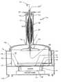
- FIG. 1is a schematic representation of a prior art remote PECVD chamber 10 .
- these remote PECVD chambersprovide for RF coils 12 surrounding a tube 14 , typically a pyrex tube, to inductively excite a gas delivered at the top 16 of reactor 10 .
- the excited gasis then transported into chamber 20 through input port 18 .
- the gasdisperses within chamber 20 and reacts with substrate 22 which is supported on pedestal 24 .
- a similar PECVD chamberhas been previously discussed by D. V.
- a second gasis delivered through a feed-through tube to a gas dispersal ring that is placed over the substrate. This second gas is typically delivered through a second input port, shown in FIG. 1 as covered by plate 19 .
- the second gas delivery apparatusi.e., gas dispersal ring
- gas dispersal ringis not common to all prior art remote PECVD chambers, it nevertheless further contributes to gas concentration non-uniformity at the wafer surface. It also represents a current prior art method for introducing a second, unexcited gas into the chamber.
- Process uniformityhas been previously attempted by establishing the flow dynamics that help control a uniform species distribution across the reacting surface.
- An inherent disadvantage of a remote plasma systemis the lack of acceptable process uniformity of the gas distribution at the wafer or substrate level. Since the active gases created by the plasma are delivered to the process chamber and not created in it, the distribution of gases inside the chamber is very difficult to control due to unwanted reactions on the chamber surfaces which consume the active gases. If the reactive gas flows in from the side of the reactor, with respect to the wafer, the concentration will be high in the center of the wafer and low at the edges.
- a showerheadis used to make the gas distribution uniform over the wafer. This strategy is not suitable for downstream reactors because the active gasses would have to flow past the baffle and faceplate holes which make up the showerhead.
- the showerhead elementsalso have the effect of destroying the active species needed for remote processing.
- the showerhead elementspromote recombination.
- the showerhead elementspromote “quenching” or deactivation of the species.
- the distribution of gas during plasma processingcan be also be affected by the introduction of a second gas.
- Concurrent injection of two gases (or gas mixtures)is typically performed by introducing the second (unexcited) gas through a separate input port into the chamber.
- this second injectionwill alter the uniform distribution of the excited gas, requiring that at least two separate distribution normalization systems or processes be employed.
- An apparatus and method capable of concurrent injection through the same input portwould allow for unique advantages in the distribution normalization of the gas mixture, and eliminate the need for a second input to the chamber.
- a supersonic CVD gas jet source for deposition of thin filmshas been developed in U.S. Pat. No. 5,256,205, issued to J. Schmitt, et al., entitled “MICROWAVE PLASMA ASSISTED SUPERSONIC GAS JET DEPOSITION OF THIN FILM MATERIALS.”
- This sourcehas been used to produce a high dielectric constant for thin film semiconductor applications, e.g., Si 3 N 4 .
- this sourcedoes not provide for simultaneous delivery of active and molecular (non-activated or dissociated) gas species.
- prior art sources of concurrent gas delivery systemsare limited to an area at the wafer surface about 1 cm to 2 cm in diameter, restricted mainly by the Laval nozzle dimension, and require translation of the substrate in a complex motion in front of the nozzle in order to achieve deposition over an entire substrate of any dimension greater than approximately 1 cm.
- a further object of the inventionis to provide an apparatus and method for varying the gas concentration distribution across a wafer in a remote PECVD process.
- Another object of the inventionis to provide a remote PECVD source that can deposit uniform thin films across the entire field of the substrate with no movement or translation of the substrate or source.
- a further object of the present inventionis to provide an apparatus and method to introduce gases into the chamber concurrently, through the plasma tube, having one gas excited by the plasma tube energies and the other remaining unexcited and shielded from the plasma tube energies.
- a method for modifying gas flow distribution during chemical vapor deposition on a substrate within a remote plasma reactor chambercomprising the steps of: a) establishing a remote plasma region by exciting a gas mixture with RF energy in a location removed from the chamber; b) injecting the gas mixture into the plasma region; c) transporting the excited gas mixture from the remote plasma region through an input port into the chamber; and, d) distributing the excited gas mixture over the substrate to a predetermined profile.
- the methodfurther includes causing the excited gas mixture to diffuse from the remote plasma region inward toward the chamber.
- the methodalso includes, in step (d), adjusting a contoured plate by changing the distance from the plate to the substrate to establish the predetermined profile.
- the predetermined profilecomprises a wafer-edge concentrated distribution or a wafer-center concentrated distribution.
- the inventionis directed to a method for modifying gas flow distribution during deposition on a substrate within a remote plasma reactor chamber, comprising the steps of: a) establishing a remote plasma region by exciting a gas mixture with RF energy in a location removed from the chamber; b) transporting the excited gas mixture from the remote plasma region through an input port in the chamber; c) redistributing the transported gas mixture within the chamber by providing a contoured plate of predetermined diameter between the input port and the substrate, the plate having a distance to the substrate; and, d) adjusting the distance to modify the gas flow distribution to the substrate.
- the inventionis directed to a remote plasma reactor for processing a workpiece, comprising: a chamber enclosure having an input port; a remote plasma source connected to the input port and adapted to provide a means for gas transport from the source to the chamber through the input port; an inductive coil surrounding a portion of the remote plasma source capable of inductively coupling RF energy from an RF power supply; a pedestal within the chamber defining thereon a workstation to support the workpiece; and, a profiler plate within the chamber and mounted between the input port and the workpiece, the profiler plate being contoured and having a predetermined diameter and placed a predetermined distance from the workpiece.
- the profiler plateis symmetric about a center axis, having a narrow top portion and a wide bottom portion, the narrow top portion mounted closest to the input port and the axis centered with the input port.
- the inventionis directed to an apparatus for modifying the gas distribution within a remote plasma enhanced chemical vapor deposition reactor having a chamber with an input port, the apparatus comprising: an axial symmetrical plate having a narrow top end and a bottom end wider than the top end, and centered with respect to the input port; and, an adjustable height securing clamp connecting the plate to the reactor adjacent to the input port.
- the present inventionis directed to an apparatus for concurrently administering at least two gases into a plasma excitation region of a remote plasma enhanced chemical vapor deposition reactor, comprising: a chamber having at least one input port for the gas delivery and a pedestal for securing a semiconductor wafer; a coaxial injector tube attached to the chamber, including: an outer tube for confining a first gas for plasma excitation and defining the plasma excitation region; and, an inner tube within the outer tube, for delivery of a second gas through the plasma excitation region such that the second gas remains unexcited after traversing through the plasma region.
- the inner tubepasses axially and concentrically through the length of the outer tube and the tubes are comprised of a dielectric material.
- the inner tubefurther comprises: a metal gas tube; a dielectric inner sleeve external to and axially concentric with the metal gas tube; a Faraday shield external to and axially concentric with the dielectric inner sleeve; and, a dielectric outer sleeve external to and axially concentric with the Faraday shield.
- the Faraday shieldmay also include an infrared reflective coating.
- the present inventionis directed to, in a sixth aspect, an apparatus for administering gas into a plasma excitation region of a remote plasma enhanced chemical vapor deposition reactor, comprising: a chamber having at least one input port for the gas delivery and a pedestal for securing a semiconductor wafer; a coaxial injector tube having a top end and a bottom end, attached to the chamber at the bottom end, including: an outer tube confining a first gas for plasma excitation and defining the plasma excitation region; and, an inner tube within the outer tube, for delivery of a second gas through the plasma excitation region such that the second gas remains unexcited after traversing through the plasma excitation region; and, a contoured plate having a center hole, slideably attached to the coaxial injector tube through the center hole.
- the present inventionis directed to, in a seventh aspect, a method for injecting two gas mixtures into a remote plasma enhanced chemical vapor deposition reactor such that a first gas is excited by plasma energy while a second gas remains unexcited by the plasma energy, the method comprising: a) providing the remote plasma enhanced chemical vapor deposition reactor having a remote plasma source, a chamber, and one input port for gas ingress into the chamber; b) establishing a plasma region by applying RF energy to energize plasma in the remote plasma source; c) injecting the first and second gases into the plasma region to the chamber through the input port; d) exciting the first gas with the plasma energy; and, e) shielding the second gas from the plasma energy such that the second gas remains in a non-excited state as it traverses through the energized plasma region.
- the present inventionis directed to a method for injecting two gas mixtures into a remote plasma enhanced chemical vapor deposition reactor such that a first gas is excited by plasma energy while a second gas remains unexcited by the plasma energy, and normalizing the distribution of the gases on a wafer surface, the method comprising: a) providing the remote plasma enhanced chemical vapor deposition reactor having a remote plasma source, a chamber, and one input port for gas ingress into the chamber; b) adjusting and securing a contoured plate of predetermined diameter below the input port and above the wafer surface; c) establishing a plasma region by applying RF energy to energize plasma in the remote plasma source; d) injecting the first and second gases into the plasma region to the chamber through the input port and towards the plate; e) exciting the first gas with the plasma energy; and, f) shielding the second gas from the plasma energy such that the second gas remains in a non-excited state as it traverses through the plasma region.
- FIG. 1is a schematic representation of a prior art remote PECVD reactor.
- FIG. 2is an elevated cross-sectional view of a remote PECVD reactor with a contoured plate implemented for gas distribution.
- FIG. 3is a computer generated distribution calculation using a contoured plate in a remote plasma reactor chamber.
- FIG. 4depicts a normalized N 2 * concentration across the wafer as a function of wafer to profiler distance.
- FIG. 5depicts an elevated cross-sectional view of a coaxial remote plasma source and chamber.
- FIG. 6Ais an elevated cross-sectional view of the multiple layers of the coaxial injector tube.
- FIG. 6Bis a top view of a remote PECVD reactor having a profiler and coaxial injector tube.
- FIGS. 1 - 6 of the drawingsin which like numerals refer to like features of the invention.
- Features of the inventionare not necessarily shown to scale in the drawings.
- This inventionprovides an apparatus and method for tailoring the distribution of an active species generated by the remote plasma source over the substrate or wafer.
- the distributionmay be made more or less uniform, wafer-edge concentrated, or wafer-center concentrated depending upon the needs of the particular process.
- the present inventionsubstantially allows for uniformity of the gas concentration of meta-stable or atomic species in a downstream (remote) plasma reactor.
- the preferred embodimentconsiders the deposition of a film of Silicon Nitride, but neither the current invention nor the remote PECVD method are restricted to a given film type.
- this inventionrelates to an axially symmetric contoured plate, hereinafter referred to as a profiler, capable of adjustment for modifying the active species concentration in a downstream reactor.
- a profilercapable of adjustment for modifying the active species concentration in a downstream reactor.
- a predetermined distribution of the active gas over the wafercan be achieved in a remote PECVD process.
- the method using the profiler to modify the gas concentrationis also delineated.
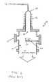
- FIG. 2A preferred apparatus is illustrated in FIG. 2.
- the active gasis generated in the plasma source. Gas flows from conduit 36 to the excitation tube 34 .
- the gasis inductively excited by RF energy as it passes through tube 34 surrounded by coils 32 .
- the active gasenters chamber 40 through input port 28 .
- the gasis redistributed by a profiler 46 .
- the direction of the gas, over profiler 46is indicated by arrows 38 .
- the profileris an axially symmetric contoured plate, having a narrow top end and a wider bottom end. As shown, the profiler is centered between the input port 28 and the wafer 42 .
- the profileris shaped to redistribute the gas flow incident upon it.
- the profileris constructed of, or coated with, a material that inhibits recombination of meta-stable species quenching, for example Teflon, and the like. This minimizes the loss of reactive species.
- a material that inhibits recombination of meta-stable species quenchingfor example Teflon, and the like. This minimizes the loss of reactive species.
- the reactive speciesdiffuses from the outside of the chamber toward the inside of the chamber.
- the distribution of the active species over the waferis controlled by the diameter of the profiler, D 1 , and the distance D 2 from the wafer.
- the wafer 42remains supported within the chamber by a pedestal 44 .
- FIG. 3depicts the distribution of the active species (active gas) as calculated by this model.
- the profilercauses the active species to diffuse from the outside of the reactor inward. This allows the distribution of the active species over the wafer to be tailored to a desired profile.
- the gasis an excited molecular nitrogen, N 2 *, but the distribution has been shown to be similar for meta-stable nitrogen atom, N* (a nitrogen atom in an excited state), primarily because both are consumed through surface reactions.
- a distribution spectrum 50is shown between the chamber wall 48 and the profiler 46 . Bar chart 52 delineates the various distribution of density levels calculated.
- the higher densities levels 54 , 56are furthest from the wafer 42 for a given distance D 2 from the profiler. At different distances below the profiler, regions may be found where the distribution is concentrated at the wafer edges, concentrated at the center of the wafer, or more uniformly distributed about the wafer. For this calculation, the profiler to wafer distance is five (5) inches.
- FIG. 4shows a normalized N 2 * concentration across the wafer as a function of wafer to profiler distance D 2 , simulated for various distances: close to the wafer (small distance); further from the wafer (intermediate distance); and farthest from the wafer (large distance).
- Curves 60 , 62 , and 64depict the normalized concentration levels as a function of distance D 2 from the profiler to the wafer.
- the abscissarepresents the normalized wafer radius, with “0” indicating the wafer center and “1.0” indicating the edge of the wafer. For this calculation, 1.0 represented a 100 mm wafer radius, for a 200 mm diameter wafer.
- the distribution of active species over the wafercan be tailored to any desired shape or made uniform with the use of the profiler.
- the N 2 * concentrationmay be regulated to have a greater concentration or density at the edge of the wafer than at the center.
- curve 60depicts the reverse concentration condition; having a greater density at the waver center rather than at the wafer edge. As shown, these different concentration distributions are regulated by the profiler distance to the wafer.
- the profilersolves a long standing uniformity problem inherent to remote plasma deposition systems in a simple and inexpensive manner. It allows the distribution of the active species not only to be made more uniform, but also to be tailored to the needs of the process.
- a coaxial remote PECVD source for the concurrent injection of activated and non-activated gas specieshas been developed to allow two gases (or gas mixtures) to be delivered in an axially symmetric manner whereby one gas can be excited in a high density RF plasma, while the other gas can be prevented from excitation and/or dissociation caused by exposure to the plasma or heated surfaces in the source apparatus.
- remote PECVD of silicon nitridecould be accomplished using concurrent injection of a nitrogen containing gas, e.g., He/N 2 , He/NH 3 , and a silicon containing gas, e.g., He/SiH 4 , such that the former gas is activated in the source and the latter is not.
- a nitrogen containing gase.g., He/N 2 , He/NH 3
- a silicon containing gase.g., He/SiH 4
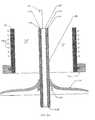
- a coaxial remote plasma source 70 and chamber 86are depicted.
- the remote plasma sourceincludes two concentric tubes, an outer tube 72 used for plasma confinement and excitation, and an inner coaxial tube 84 used for importing gas to the chamber while shielding the gas from excitation.
- the chamberconsists of a chamber dome 94 and an M2i chamber 96 .
- a process confinement shield 100encloses the process reactions.
- Substrate 90is held in place on a pedestal using clamp ring 92 .
- the substrateis heated through heater 108 , mounted on heater flange 110 .
- a clamp lift pin 112provides support from heater flange 110 to a lift ring shield 114 .
- An annular gas ring 102is mounted over substrate 90 to provide another input for gas into the chamber.
- a gas ring supply line 104connects to annular gas ring 102 and provides an input port to the chamber.
- the chamberalso includes a port 106 for a process pump.
- the compact coaxial remote plasma source 70well suited for remote PECVD, consists of the outer plasma confinement tube or sleeve 72 which can be made of a suitable dielectric material, e.g., quartz, alumina, and the like.
- the tubeis closed at the top end to atmosphere by an upper vacuum flange 74 . At the lower end, it is open to the process chamber, but closed to atmosphere by a lower vacuum flange 76 .
- An external RF coil 78is wound about the plasma confinement tube 72 . Preferably, the coil is wound in two to twelve turns.
- Gas inlet lines 80 , 82entering at the top of the plasma confinement tube through the upper vacuum flange 74 , provide injection ports for introduction of the desired gases or gas admixtures, e.g., He, Ar, He/N 2 , He/O 2 , and the like, to the plasma region 75 .
- gases or gas admixturese.g., He, Ar, He/N 2 , He/O 2 , and the like
- the RF coils 78are connected to a suitable RF generator or power supply (not shown).
- the power supply frequencymay vary, typically ranging from 400 KHz to the preferred value of 13.56 MHz at less than 1 kilowatt, but may also be at higher frequencies and higher power.
- the RF connectionsare typically made through an RF matchbox, and the coils are energized at the beginning of the deposition process.
- the gas admixturee.g., He/N 2 , He/O 2 , O 2 , N 2 , Ar/N 2 , He/N 2 , Ar/O 2 , He, Ar, He/H 2 , or H 2
- passing through the coupled RF fieldproduces a high-density plasma and the desired activated gas species, e.g., meta-stable helium, He*, atomic nitrogen, N*, excited molecular nitrogen, N 2 *, ionized molecular nitrogen, N 2 *, atomic oxygen, O*, and the like.
- the activated gas speciesexit the lower end of the tube into the process chamber 86 , where they diffuse to the surface of the wafer.
- the excited gasesmay be distributed by a modified profiler 130 , diffusing the gasses in the manner previously described.
- the coaxial injector tube assembly 84passes concentrically through the length of the plasma confinement tube 72 .
- the lower end of the injector tube, the coaxial injector exit 88is also open to the process chamber 86 .
- a gas or gas admixturee.g., He/SiH 4 , which is not to be excited or dissociated prior to contact with the surface of wafer 90 , is transported via the coaxial gas inlet 85 at the upper vacuum flange 74 through the high density plasma region 75 to process chamber 86 .
- the non-excited gasesdo not traverse around profiler 130 , rather, the coaxial injector tube exit 88 opens below the profiler plate. This allows the non-excited gases to mix with a more uniformly distributed excited gas from the plasma source region.
- the non-excited gas and the excited gasmay be the same type of gas. This allows for the simultaneous introduction of a gas within the reactor from a single source that will ultimately have an excited component and a non-excited component. The independent excited portion of the gas would then flow incident on profiler 130 and combine with its non-excited counterpart delivered through the coaxial injector tube exit port 88 .
- Gas exiting the coaxial injector tubediffuses to the surface of the heated substrate where it is free to react with the activated gas species produced in the plasma region 75 of the plasma confinement tube 72 , thereby resulting in the formation of the desired thin film on the substrate.
- the gas admixturee.g., SiH 4
- the innermost gas tube 120 of the coaxial injector tube 84preferably made of stainless steel, Al, Al alloys, Ti, or Mo, and the like, is both a conduit for the gas admixture and a grounded RF shield 121 .
- RF energy radiating from the RF coils 78 into the plasma confinement tube 72will be absorbed in the metal tube 120 and shunted to ground.
- the remote source apparatusutilizes the walls of this central metal coaxial injector tube 84 as an RF shield to prevent the gas admixture in the central tube from igniting a plasma or becoming excited (ionized) during transit through the high density RF plasma region of the outer tube.
- the RF shieldmay also incorporate an infrared reflective metal Faraday shield 122 , external to the central injector tube 120 , to prevent thermal decomposition or cracking of species in the gas admixture caused by plasma-radiation heating or induction heating of the inner wall surface.
- the metallic Faraday shieldover coated with a highly IR-reflective material, e.g., rhodium and the like, serves to reflect IR radiation from the plasma region that would otherwise heat the inner tube walls.
- a highly IR-reflective materiale.g., rhodium and the like
- Other embodiments of the basic ideainclude simplifying the design by replacing the metal inner tube with a quartz tube, and to depend upon the Faraday shield alone to reduce the RF fields in the tube to levels below that required for plasma excitation.
- the RF fieldmay also induce eddy currents in a directly exposed metallic tube. This could result in induction heating of the tube walls, which could result in gas dissociation if sufficiently high temperatures were reached.
- the copper Faraday shield 122is wrapped about the metal innermost gas tube 120 . By design, the Faraday shield inhibits the circulation of eddy currents thereby substantially eliminating induction heating.
- An inner quartz dielectric sleeve 124may be inserted between the metal gas tube 120 and the copper Faraday shield 122 to minimize direct thermal contact (coupling) between the metallic parts and to discourage the formation of unwanted plasma discharges in this region.
- a Faraday slit 123may also be designed into the shield structure to facilitate the elimination of eddy currents.
- the metal gas tube 120 , inner quartz dielectric sleeve 124 , and Faraday shield 122are enclosed within an outer quartz dielectric tube 126 .
- This outer quartz tubeserves to sleeve and isolate the inner components from the plasma discharge in the plasma confinement tube 72 , and also represents a vacuum barrier between the source interior and the atmosphere.
- This vacuum barrier or seal 128is closed at the lower end of the outer quartz dielectric sleeve 126 and metal gas tube 120 by fusing the outer quartz sleeve to the metal tube 120 .
- this sealis accomplished through an SST-Kovar-glass intermediary.
- a modified profiler 130may be used with the coaxial injector tube to regulate the distribution uniformity of the gases in the same manner as previously discussed.
- the profileris modified to accept the coaxial injector tube through a hole at its center.
- Height adjustment clamps 132are located on the profiler to secure the profiler to the coaxial injector tube and regulate the distance from the profiler to the substrate. The profiler distributes the excited gas while allowing the non-excited gas to traverse through its center toward the substrate.
- FIG. 6Bdepicts a top view of profiler 130 in a remote PECVD reactor. The axial symmetry is shown along with the coaxial injector tube 84 wound with RF coils 78 and traversing through the center aperture of the profiler.
- the method for simultaneously injecting two gas mixtures into a chamber of a remote plasma enhanced chemical vapor deposition reactorincludes ensuring that the first gas is excited by plasma energy while the second gas remains unexcited by the plasma energy.
- This methodincludes the steps of: a) providing a remote plasma enhanced chemical vapor deposition reactor that has a coaxial injector tube connecting to one main input port for gas ingress into the chamber; b) establishing the plasma region by applying RF energy to energize plasma in the plasma confined region; c) injecting two gas mixtures into the plasma region to the chamber through the input port; d) exciting one of the gas mixtures with the plasma energy; and, e) shielding the second gas from the plasma energy such that the second gas remains in a non-excited state as it traverses through the energized plasma region.
- both gases or gas mixturestraverse through the same plasma tube while the plasma tube is excited by RF coils surrounding the plasma tube's outer surface.
- the coaxial injector tubeshields one of the injected gases from the plasma energy.
- this shieldcan be either an electrical shield (Faraday shield), an IR shield, or both.
Landscapes
- Chemical & Material Sciences (AREA)
- Engineering & Computer Science (AREA)
- General Chemical & Material Sciences (AREA)
- Chemical Kinetics & Catalysis (AREA)
- Materials Engineering (AREA)
- Mechanical Engineering (AREA)
- Metallurgy (AREA)
- Organic Chemistry (AREA)
- Physics & Mathematics (AREA)
- Plasma & Fusion (AREA)
- Analytical Chemistry (AREA)
- Chemical Vapour Deposition (AREA)
Abstract
Description
- 1. Field of the invention[0001]
- The present invention relates to a plasma reactor, specifically, to a method and apparatus used in the manufacture of integrated circuits and other electronic devices. More particularly, the invention relates to modifying and uniformly distributing the gas concentration of a meta-stable or atomic species over a wafer in a downstream plasma reactor.[0002]
- 2. Description of Related Art[0003]
- Plasma-based reactions have become increasingly important to the semiconductor industry, providing for precisely controlled thin-film depositions, thin film etching, and surface treatment such as cleaning. In a deposition process, thin films are applied to semiconductor wafers; whereas, an etching process is generally used in semiconductor manufacture to remove exposed portions of the deposited film for the purpose of patterning the film. One possible method for depositing films, such as a nitride film, is a remote plasma technique. In this method, a plasma is generated at a location which is separate from the wafer. Unlike non-remote plasma processes, downstream plasma processing allows for non-wet chemical processing while eliminating plasma-induced device damage. The plasma products are allowed to flow over the wafer. In this manner, the wafer is not subjected to ion or electron bombardment, or the high heat loads typical of in-situ plasma systems. The plasma source is also equally appropriate for etching and cleaning as it is for depositing.[0004]
- Candidates for downstream processing are those reactions initiated by atomic species or molecular fragments that can be generated within an active (glowing) plasma. Downstream processing generates a chemical reaction between reactive gas effluents flowing from the plasma source and the materials on the wafer. Downstream reactions are driven by the concentration and flow speed of the reactant flux to the wafer surface, the reaction rate constant, and the removal of reaction products from the reaction site. One difficulty arises, however, when a non-excited gas is required to be injected into the chamber concurrently with an excited gas. Typically, two independent chamber input ports are needed to supply both gases. The introduction of gases from two separate ports complicates the distribution of the gas mixture over the wafer surface leading to film non-uniformity.[0005]
- The remote plasma enhanced chemical vapor deposition (PECVD) process affords greater control over the thin-film chemistry than the conventional PECVD process by restricting plasma excitation to a subset of the process gases, and thereby reducing the number of possible reaction pathways. The physical arrangement of a remote PECVD chamber is designed to make the process flow sequential or serial, rather than parallel as in a conventional or direct PECVD processes. A description of a remote PECVD process can be found in J. A. Theil, et al., “EFFECTS OF NH[0006]3AND N2SOURCE GASES AND PLASMA EXCITATION FREQUENCIES ON THE REACTION CHEMISTRY FOR Si3N4THIN-FILM GROWTH BY REMOTE PLASMA-ENHANCED CHEMICAL-VAPOR DEPOSITION”, J. Vac. Sci. Technology, A 10(4), July/August 1992, pp. 719-727.
- Typically, a remote PECVD deposition process consists of the following steps: a) RF excitation of a first gas or gas mixture; b) transport of the excited species out of the plasma region into a chamber; c) introduction of a second gas over the substrate surface; and d) a CVD reaction at a substrate supported within the chamber to generate a thin dielectric film. For example, if a thin film silicon nitride were desired, the first gas would contain nitrogen, and the second gas would include a silicon containing gas such as Silane, SiH[0007]4.
- FIG. 1 is a schematic representation of a prior art remote PECVD chamber[0008]10. Importantly, these remote PECVD chambers provide for RF coils12 surrounding a
tube 14, typically a pyrex tube, to inductively excite a gas delivered at thetop 16 of reactor10. The excited gas is then transported intochamber 20 throughinput port 18. The gas disperses withinchamber 20 and reacts with substrate22 which is supported onpedestal 24. A similar PECVD chamber has been previously discussed by D. V. Tsu, et al., in “LOCAL ATOMIC STRUCTURE IN THIN FILMS OF SILICON NITRIDE AND SILICON DIIMIDE PRODUCED BY REMOTE PLASMA-ENHANCED CHEMICAL-VAPOR DEPOSITION,” Physical Review B, Volume 33, Number 10, May 15, 1996, p. 7070. In the Tsu invention, a second gas is delivered through a feed-through tube to a gas dispersal ring that is placed over the substrate. This second gas is typically delivered through a second input port, shown in FIG. 1 as covered byplate 19. Although the second gas delivery apparatus, i.e., gas dispersal ring, is not common to all prior art remote PECVD chambers, it nevertheless further contributes to gas concentration non-uniformity at the wafer surface. It also represents a current prior art method for introducing a second, unexcited gas into the chamber. - Process uniformity has been previously attempted by establishing the flow dynamics that help control a uniform species distribution across the reacting surface. An inherent disadvantage of a remote plasma system, however, is the lack of acceptable process uniformity of the gas distribution at the wafer or substrate level. Since the active gases created by the plasma are delivered to the process chamber and not created in it, the distribution of gases inside the chamber is very difficult to control due to unwanted reactions on the chamber surfaces which consume the active gases. If the reactive gas flows in from the side of the reactor, with respect to the wafer, the concentration will be high in the center of the wafer and low at the edges.[0009]
- In typical (non-remote) Chemical Vapor Deposition (CVD) or Plasma Enhanced Chemical Vapor Deposition (PECVD) reactors, a showerhead is used to make the gas distribution uniform over the wafer. This strategy is not suitable for downstream reactors because the active gasses would have to flow past the baffle and faceplate holes which make up the showerhead. The showerhead elements also have the effect of destroying the active species needed for remote processing.[0010]
- In the case of an active atomic species being generated in the remote plasma, the showerhead elements promote recombination. In the case where the remote plasma generates a meta-stable species, the showerhead elements promote “quenching” or deactivation of the species.[0011]
- The distribution of gas during plasma processing can be also be affected by the introduction of a second gas. Concurrent injection of two gases (or gas mixtures) is typically performed by introducing the second (unexcited) gas through a separate input port into the chamber. However, this second injection will alter the uniform distribution of the excited gas, requiring that at least two separate distribution normalization systems or processes be employed. An apparatus and method capable of concurrent injection through the same input port would allow for unique advantages in the distribution normalization of the gas mixture, and eliminate the need for a second input to the chamber.[0012]
- Additionally, concurrently providing two independent gases to the chamber through the same plasma confinement tube, one gas of which is excited by the plasma source while the other is isolated from the RF inductive and infrared radiated energies, facilitates the simultaneous introduction of diverse gas mixtures within the process chamber. Also, one may introduce a single gas within the chamber causing it to have an excited component and a non-excited component.[0013]
- A supersonic CVD gas jet source for deposition of thin films has been developed in U.S. Pat. No. 5,256,205, issued to J. Schmitt, et al., entitled “MICROWAVE PLASMA ASSISTED SUPERSONIC GAS JET DEPOSITION OF THIN FILM MATERIALS.” This source has been used to produce a high dielectric constant for thin film semiconductor applications, e.g., Si[0014]3N4. However, this source does not provide for simultaneous delivery of active and molecular (non-activated or dissociated) gas species.
- Also, it is advantageous to have a source that is not dependent upon the supersonic flow of the material to be deposited on the semiconductor substrate. It is beneficial to have material transport and growth not made dependent only upon diffusion kinetics in high vacuum, e.g., 300 mTorr. Less process gas flow at lower chamber pressures will reduce chamber design and construction constraints.[0015]
- Lastly, prior art sources of concurrent gas delivery systems are limited to an area at the wafer surface about 1 cm to 2 cm in diameter, restricted mainly by the Laval nozzle dimension, and require translation of the substrate in a complex motion in front of the nozzle in order to achieve deposition over an entire substrate of any dimension greater than approximately 1 cm.[0016]
- Bearing in mind the problems and deficiencies of the prior art, it is therefore an object of the present invention to provide an apparatus and method for injecting gases and enhancing the uniformity of the active species in a remote downstream plasma reactor.[0017]
- It is another object of the present invention to provide an apparatus and method for tailoring the gas concentration distribution of a remote PECVD process for wafer-edge or wafer-center concentrations.[0018]
- A further object of the invention is to provide an apparatus and method for varying the gas concentration distribution across a wafer in a remote PECVD process.[0019]
- Another object of the invention is to provide a remote PECVD source that can deposit uniform thin films across the entire field of the substrate with no movement or translation of the substrate or source.[0020]
- It is yet another object of the present invention to provide a remote PECVD process that minimizes the loss of reactive species.[0021]
- A further object of the present invention is to provide an apparatus and method to introduce gases into the chamber concurrently, through the plasma tube, having one gas excited by the plasma tube energies and the other remaining unexcited and shielded from the plasma tube energies.[0022]
- Still other advantages of the invention will in part be obvious and will in part be apparent from the specification.[0023]
- The above and other advantages, which will be apparent to one of skill in the art, are achieved in the present invention which is directed to, in a first aspect, a method for modifying gas flow distribution during chemical vapor deposition on a substrate within a remote plasma reactor chamber, comprising the steps of: a) establishing a remote plasma region by exciting a gas mixture with RF energy in a location removed from the chamber; b) injecting the gas mixture into the plasma region; c) transporting the excited gas mixture from the remote plasma region through an input port into the chamber; and, d) distributing the excited gas mixture over the substrate to a predetermined profile.[0024]
- The method further includes causing the excited gas mixture to diffuse from the remote plasma region inward toward the chamber. The method also includes, in step (d), adjusting a contoured plate by changing the distance from the plate to the substrate to establish the predetermined profile. The predetermined profile comprises a wafer-edge concentrated distribution or a wafer-center concentrated distribution.[0025]
- In a second aspect, the invention is directed to a method for modifying gas flow distribution during deposition on a substrate within a remote plasma reactor chamber, comprising the steps of: a) establishing a remote plasma region by exciting a gas mixture with RF energy in a location removed from the chamber; b) transporting the excited gas mixture from the remote plasma region through an input port in the chamber; c) redistributing the transported gas mixture within the chamber by providing a contoured plate of predetermined diameter between the input port and the substrate, the plate having a distance to the substrate; and, d) adjusting the distance to modify the gas flow distribution to the substrate.[0026]
- In a third aspect, the invention is directed to a remote plasma reactor for processing a workpiece, comprising: a chamber enclosure having an input port; a remote plasma source connected to the input port and adapted to provide a means for gas transport from the source to the chamber through the input port; an inductive coil surrounding a portion of the remote plasma source capable of inductively coupling RF energy from an RF power supply; a pedestal within the chamber defining thereon a workstation to support the workpiece; and, a profiler plate within the chamber and mounted between the input port and the workpiece, the profiler plate being contoured and having a predetermined diameter and placed a predetermined distance from the workpiece.[0027]
- The profiler plate is symmetric about a center axis, having a narrow top portion and a wide bottom portion, the narrow top portion mounted closest to the input port and the axis centered with the input port.[0028]
- In a fourth aspect, the invention is directed to an apparatus for modifying the gas distribution within a remote plasma enhanced chemical vapor deposition reactor having a chamber with an input port, the apparatus comprising: an axial symmetrical plate having a narrow top end and a bottom end wider than the top end, and centered with respect to the input port; and, an adjustable height securing clamp connecting the plate to the reactor adjacent to the input port.[0029]
- In a fifth aspect, the present invention is directed to an apparatus for concurrently administering at least two gases into a plasma excitation region of a remote plasma enhanced chemical vapor deposition reactor, comprising: a chamber having at least one input port for the gas delivery and a pedestal for securing a semiconductor wafer; a coaxial injector tube attached to the chamber, including: an outer tube for confining a first gas for plasma excitation and defining the plasma excitation region; and, an inner tube within the outer tube, for delivery of a second gas through the plasma excitation region such that the second gas remains unexcited after traversing through the plasma region.[0030]
- The inner tube passes axially and concentrically through the length of the outer tube and the tubes are comprised of a dielectric material. The inner tube further comprises: a metal gas tube; a dielectric inner sleeve external to and axially concentric with the metal gas tube; a Faraday shield external to and axially concentric with the dielectric inner sleeve; and, a dielectric outer sleeve external to and axially concentric with the Faraday shield. The Faraday shield may also include an infrared reflective coating.[0031]
- The present invention is directed to, in a sixth aspect, an apparatus for administering gas into a plasma excitation region of a remote plasma enhanced chemical vapor deposition reactor, comprising: a chamber having at least one input port for the gas delivery and a pedestal for securing a semiconductor wafer; a coaxial injector tube having a top end and a bottom end, attached to the chamber at the bottom end, including: an outer tube confining a first gas for plasma excitation and defining the plasma excitation region; and, an inner tube within the outer tube, for delivery of a second gas through the plasma excitation region such that the second gas remains unexcited after traversing through the plasma excitation region; and, a contoured plate having a center hole, slideably attached to the coaxial injector tube through the center hole.[0032]
- The present invention is directed to, in a seventh aspect, a method for injecting two gas mixtures into a remote plasma enhanced chemical vapor deposition reactor such that a first gas is excited by plasma energy while a second gas remains unexcited by the plasma energy, the method comprising: a) providing the remote plasma enhanced chemical vapor deposition reactor having a remote plasma source, a chamber, and one input port for gas ingress into the chamber; b) establishing a plasma region by applying RF energy to energize plasma in the remote plasma source; c) injecting the first and second gases into the plasma region to the chamber through the input port; d) exciting the first gas with the plasma energy; and, e) shielding the second gas from the plasma energy such that the second gas remains in a non-excited state as it traverses through the energized plasma region.[0033]
- In an eighth aspect, the present invention is directed to a method for injecting two gas mixtures into a remote plasma enhanced chemical vapor deposition reactor such that a first gas is excited by plasma energy while a second gas remains unexcited by the plasma energy, and normalizing the distribution of the gases on a wafer surface, the method comprising: a) providing the remote plasma enhanced chemical vapor deposition reactor having a remote plasma source, a chamber, and one input port for gas ingress into the chamber; b) adjusting and securing a contoured plate of predetermined diameter below the input port and above the wafer surface; c) establishing a plasma region by applying RF energy to energize plasma in the remote plasma source; d) injecting the first and second gases into the plasma region to the chamber through the input port and towards the plate; e) exciting the first gas with the plasma energy; and, f) shielding the second gas from the plasma energy such that the second gas remains in a non-excited state as it traverses through the plasma region.[0034]
- The features of the invention believed to be novel and the elements characteristic of the invention are set forth with particularity in the appended claims. The figures are for illustration purposes only and are not drawn to scale. The invention itself, however, both as to organization and method of operation, may best be understood by reference to the detailed description which follows taken in conjunction with the accompanying drawings in which:[0035]
- FIG. 1 is a schematic representation of a prior art remote PECVD reactor.[0036]
- FIG. 2 is an elevated cross-sectional view of a remote PECVD reactor with a contoured plate implemented for gas distribution.[0037]
- FIG. 3 is a computer generated distribution calculation using a contoured plate in a remote plasma reactor chamber.[0038]
- FIG. 4 depicts a normalized N[0039]2* concentration across the wafer as a function of wafer to profiler distance.
- FIG. 5 depicts an elevated cross-sectional view of a coaxial remote plasma source and chamber.[0040]
- FIG. 6A is an elevated cross-sectional view of the multiple layers of the coaxial injector tube.[0041]
- FIG. 6B is a top view of a remote PECVD reactor having a profiler and coaxial injector tube.[0042]
- In describing the preferred embodiment of the present invention, reference will be made herein to FIGS.[0043]1-6 of the drawings in which like numerals refer to like features of the invention. Features of the invention are not necessarily shown to scale in the drawings.
- This invention provides an apparatus and method for tailoring the distribution of an active species generated by the remote plasma source over the substrate or wafer. The distribution may be made more or less uniform, wafer-edge concentrated, or wafer-center concentrated depending upon the needs of the particular process. In this manner, the present invention substantially allows for uniformity of the gas concentration of meta-stable or atomic species in a downstream (remote) plasma reactor.[0044]
- For the purpose of illustration, the preferred embodiment considers the deposition of a film of Silicon Nitride, but neither the current invention nor the remote PECVD method are restricted to a given film type.[0045]
- In particular, this invention relates to an axially symmetric contoured plate, hereinafter referred to as a profiler, capable of adjustment for modifying the active species concentration in a downstream reactor. By modifying this concentration, a predetermined distribution of the active gas over the wafer can be achieved in a remote PECVD process. The method using the profiler to modify the gas concentration is also delineated.[0046]
- A preferred apparatus is illustrated in FIG. 2. The active gas is generated in the plasma source. Gas flows from[0047]
conduit 36 to the excitation tube34. The gas is inductively excited by RF energy as it passes through tube34 surrounded bycoils 32. The active gas enterschamber 40 throughinput port 28. Before flowing toward thewafer 42, however, the gas is redistributed by aprofiler 46. The direction of the gas, overprofiler 46, is indicated byarrows 38. The profiler is an axially symmetric contoured plate, having a narrow top end and a wider bottom end. As shown, the profiler is centered between theinput port 28 and thewafer 42. The profiler is shaped to redistribute the gas flow incident upon it. - The profiler is constructed of, or coated with, a material that inhibits recombination of meta-stable species quenching, for example Teflon, and the like. This minimizes the loss of reactive species. Once inside the process chamber, the reactive species diffuses from the outside of the chamber toward the inside of the chamber. The distribution of the active species over the wafer is controlled by the diameter of the profiler, D[0048]1, and the distance D2 from the wafer. The
wafer 42 remains supported within the chamber by apedestal 44. - Various gas concentration distribution scenarios have been verified by use of a computational fluid dynamics model of the downstream deposition system. FIG. 3 depicts the distribution of the active species (active gas) as calculated by this model. The profiler causes the active species to diffuse from the outside of the reactor inward. This allows the distribution of the active species over the wafer to be tailored to a desired profile. In this case, the gas is an excited molecular nitrogen, N[0049]2*, but the distribution has been shown to be similar for meta-stable nitrogen atom, N* (a nitrogen atom in an excited state), primarily because both are consumed through surface reactions. A
distribution spectrum 50 is shown between thechamber wall 48 and theprofiler 46. Bar chart52 delineates the various distribution of density levels calculated. As indicated, thehigher densities levels 54,56 are furthest from thewafer 42 for a given distance D2 from the profiler. At different distances below the profiler, regions may be found where the distribution is concentrated at the wafer edges, concentrated at the center of the wafer, or more uniformly distributed about the wafer. For this calculation, the profiler to wafer distance is five (5) inches. - FIG. 4 shows a normalized N[0050]2* concentration across the wafer as a function of wafer to profiler distance D2, simulated for various distances: close to the wafer (small distance); further from the wafer (intermediate distance); and farthest from the wafer (large distance).
Curves curve 64, the N2* concentration may be regulated to have a greater concentration or density at the edge of the wafer than at the center. In contrast,curve 60 depicts the reverse concentration condition; having a greater density at the waver center rather than at the wafer edge. As shown, these different concentration distributions are regulated by the profiler distance to the wafer. - The profiler solves a long standing uniformity problem inherent to remote plasma deposition systems in a simple and inexpensive manner. It allows the distribution of the active species not only to be made more uniform, but also to be tailored to the needs of the process.[0051]
- In situations where a second gas is injected within the chamber, it is beneficial to take advantage of the profiler's distribution normalization. However, this requires the second gas to be injected concurrently with the first (excited) gas. A coaxial remote PECVD source for the concurrent injection of activated and non-activated gas species has been developed to allow two gases (or gas mixtures) to be delivered in an axially symmetric manner whereby one gas can be excited in a high density RF plasma, while the other gas can be prevented from excitation and/or dissociation caused by exposure to the plasma or heated surfaces in the source apparatus.[0052]
- As a specific illustration, remote PECVD of silicon nitride could be accomplished using concurrent injection of a nitrogen containing gas, e.g., He/N[0053]2, He/NH3, and a silicon containing gas, e.g., He/SiH4, such that the former gas is activated in the source and the latter is not. This capability provides a method to increase the uniformity of distribution of the reactant gas species at the wafer surface, particularly when used in conjunction with an annular gas injection ring near the substrate surface while maintaining separation of the desired species/admixtures from the plasma region.
- Referring to FIG. 5, a coaxial[0054]
remote plasma source 70 andchamber 86 are depicted. The remote plasma source includes two concentric tubes, anouter tube 72 used for plasma confinement and excitation, and an innercoaxial tube 84 used for importing gas to the chamber while shielding the gas from excitation. The chamber consists of achamber dome 94 and an M2i chamber96. Aprocess confinement shield 100 encloses the process reactions.Substrate 90 is held in place on a pedestal usingclamp ring 92. The substrate is heated throughheater 108, mounted onheater flange 110. Aclamp lift pin 112 provides support fromheater flange 110 to alift ring shield 114. Anannular gas ring 102 is mounted oversubstrate 90 to provide another input for gas into the chamber. A gasring supply line 104 connects toannular gas ring 102 and provides an input port to the chamber. The chamber also includes aport 106 for a process pump. - The compact coaxial[0055]
remote plasma source 70, well suited for remote PECVD, consists of the outer plasma confinement tube orsleeve 72 which can be made of a suitable dielectric material, e.g., quartz, alumina, and the like. The tube is closed at the top end to atmosphere by anupper vacuum flange 74. At the lower end, it is open to the process chamber, but closed to atmosphere by alower vacuum flange 76. Anexternal RF coil 78 is wound about theplasma confinement tube 72. Preferably, the coil is wound in two to twelve turns. Gas inlet lines80,82, entering at the top of the plasma confinement tube through theupper vacuum flange 74, provide injection ports for introduction of the desired gases or gas admixtures, e.g., He, Ar, He/N2, He/O2, and the like, to theplasma region 75. - The RF coils[0056]78 are connected to a suitable RF generator or power supply (not shown). The power supply frequency may vary, typically ranging from 400 KHz to the preferred value of 13.56 MHz at less than 1 kilowatt, but may also be at higher frequencies and higher power. The RF connections are typically made through an RF matchbox, and the coils are energized at the beginning of the deposition process. The gas admixture, e.g., He/N2, He/O2, O2, N2, Ar/N2, He/N2, Ar/O2, He, Ar, He/H2, or H2, passing through the coupled RF field produces a high-density plasma and the desired activated gas species, e.g., meta-stable helium, He*, atomic nitrogen, N*, excited molecular nitrogen, N2*, ionized molecular nitrogen, N2*, atomic oxygen, O*, and the like. The activated gas species exit the lower end of the tube into the
process chamber 86, where they diffuse to the surface of the wafer. Importantly, the excited gases may be distributed by a modifiedprofiler 130, diffusing the gasses in the manner previously described. - The coaxial[0057]
injector tube assembly 84 passes concentrically through the length of theplasma confinement tube 72. As with the plasma confinement tube, the lower end of the injector tube, thecoaxial injector exit 88, is also open to theprocess chamber 86. A gas or gas admixture, e.g., He/SiH4, which is not to be excited or dissociated prior to contact with the surface ofwafer 90, is transported via thecoaxial gas inlet 85 at theupper vacuum flange 74 through the highdensity plasma region 75 to processchamber 86. The non-excited gases do not traverse aroundprofiler 130, rather, the coaxialinjector tube exit 88 opens below the profiler plate. This allows the non-excited gases to mix with a more uniformly distributed excited gas from the plasma source region. - Importantly, the non-excited gas and the excited gas may be the same type of gas. This allows for the simultaneous introduction of a gas within the reactor from a single source that will ultimately have an excited component and a non-excited component. The independent excited portion of the gas would then flow incident on[0058]
profiler 130 and combine with its non-excited counterpart delivered through the coaxial injectortube exit port 88. - Gas exiting the coaxial injector tube diffuses to the surface of the heated substrate where it is free to react with the activated gas species produced in the[0059]
plasma region 75 of theplasma confinement tube 72, thereby resulting in the formation of the desired thin film on the substrate. - Importantly, the gas admixture, e.g., SiH[0060]4, that is not to be excited or dissociated prior to contact with the wafer surface must not be directly exposed to the RF field surrounding the plasma confinement tube. Nor must the tube walls be heated appreciably by radiation emitted from the plasma. This may be accomplished in one of two ways. Referring to FIG. 6, the
innermost gas tube 120 of thecoaxial injector tube 84, preferably made of stainless steel, Al, Al alloys, Ti, or Mo, and the like, is both a conduit for the gas admixture and a groundedRF shield 121. RF energy radiating from the RF coils78 into theplasma confinement tube 72 will be absorbed in themetal tube 120 and shunted to ground. - The remote source apparatus utilizes the walls of this central metal[0061]
coaxial injector tube 84 as an RF shield to prevent the gas admixture in the central tube from igniting a plasma or becoming excited (ionized) during transit through the high density RF plasma region of the outer tube. The RF shield may also incorporate an infrared reflectivemetal Faraday shield 122, external to thecentral injector tube 120, to prevent thermal decomposition or cracking of species in the gas admixture caused by plasma-radiation heating or induction heating of the inner wall surface. The metallic Faraday shield, over coated with a highly IR-reflective material, e.g., rhodium and the like, serves to reflect IR radiation from the plasma region that would otherwise heat the inner tube walls. Other embodiments of the basic idea include simplifying the design by replacing the metal inner tube with a quartz tube, and to depend upon the Faraday shield alone to reduce the RF fields in the tube to levels below that required for plasma excitation. - The RF field may also induce eddy currents in a directly exposed metallic tube. This could result in induction heating of the tube walls, which could result in gas dissociation if sufficiently high temperatures were reached. To minimize or eliminate induction heating, the[0062]
copper Faraday shield 122 is wrapped about the metalinnermost gas tube 120. By design, the Faraday shield inhibits the circulation of eddy currents thereby substantially eliminating induction heating. An inner quartzdielectric sleeve 124 may be inserted between themetal gas tube 120 and thecopper Faraday shield 122 to minimize direct thermal contact (coupling) between the metallic parts and to discourage the formation of unwanted plasma discharges in this region. A Faraday slit123 may also be designed into the shield structure to facilitate the elimination of eddy currents. - The[0063]
metal gas tube 120, inner quartzdielectric sleeve 124, and Faraday shield122 are enclosed within an outer quartzdielectric tube 126. This outer quartz tube serves to sleeve and isolate the inner components from the plasma discharge in theplasma confinement tube 72, and also represents a vacuum barrier between the source interior and the atmosphere. This vacuum barrier or seal128 is closed at the lower end of the outer quartzdielectric sleeve 126 andmetal gas tube 120 by fusing the outer quartz sleeve to themetal tube 120. Preferably, this seal is accomplished through an SST-Kovar-glass intermediary. - As shown, a modified[0064]
profiler 130 may be used with the coaxial injector tube to regulate the distribution uniformity of the gases in the same manner as previously discussed. As depicted in FIG. 6A, the profiler is modified to accept the coaxial injector tube through a hole at its center. Height adjustment clamps132 are located on the profiler to secure the profiler to the coaxial injector tube and regulate the distance from the profiler to the substrate. The profiler distributes the excited gas while allowing the non-excited gas to traverse through its center toward the substrate. - FIG. 6B depicts a top view of[0065]
profiler 130 in a remote PECVD reactor. The axial symmetry is shown along with thecoaxial injector tube 84 wound with RF coils78 and traversing through the center aperture of the profiler. - The method for simultaneously injecting two gas mixtures into a chamber of a remote plasma enhanced chemical vapor deposition reactor includes ensuring that the first gas is excited by plasma energy while the second gas remains unexcited by the plasma energy. This method includes the steps of: a) providing a remote plasma enhanced chemical vapor deposition reactor that has a coaxial injector tube connecting to one main input port for gas ingress into the chamber; b) establishing the plasma region by applying RF energy to energize plasma in the plasma confined region; c) injecting two gas mixtures into the plasma region to the chamber through the input port; d) exciting one of the gas mixtures with the plasma energy; and, e) shielding the second gas from the plasma energy such that the second gas remains in a non-excited state as it traverses through the energized plasma region.[0066]
- Importantly, both gases or gas mixtures traverse through the same plasma tube while the plasma tube is excited by RF coils surrounding the plasma tube's outer surface. The coaxial injector tube shields one of the injected gases from the plasma energy. As previously discussed, this shield can be either an electrical shield (Faraday shield), an IR shield, or both.[0067]
- While the present invention has been particularly described, in conjunction with a specific preferred embodiment, it is evident that many alternatives, modifications and variations will be apparent to those skilled in the art in light of the foregoing description. It is therefore contemplated that the appended claims will embrace any such alternatives, modifications and variations as falling within the true scope and spirit of the present invention.[0068]
Claims (61)
1. A method for modifying gas flow distribution during chemical vapor deposition on a substrate within a remote plasma reactor chamber, comprising the steps of:
a) establishing a remote plasma region by exciting a gas mixture with RF energy in a location removed from said chamber;
b) injecting said gas mixture into said plasma region;
c) transporting the excited gas mixture from said remote plasma region through an input port into said chamber; and,
d) distributing the excited gas mixture over said substrate to a predetermined profile.
2. The method ofclaim 1 further including causing the excited gas mixture to diffuse from said remote plasma region inward toward said chamber.
3. The method ofclaim 1 wherein said gas mixture comprises meta-stable atomic nitrogen.
4. The method ofclaim 1 wherein said gas mixture comprises one of the following: molecular nitrogen, O2, N2, Ar/N2, He/N2, or Ar/O2.
5. The method ofclaim 1 wherein said step (d) further comprises adjusting an axially symmetric contoured plate by changing the distance from said plate to said substrate to establish said predetermined profile.
6. The method ofclaim 5 further comprising providing said plate with a material that inhibits recombination.
7. The method ofclaim 1 further comprising distributing the excited gas mixture over said plate while inhibiting meta-stable species quenching, said plate being coated with a material inhibiting said quenching.
8. The method ofclaim 5 wherein said plate is constructed of Teflon.
9. The method ofclaim 5 wherein said plate is coated with Teflon.
10. The method ofclaim 1 wherein said predetermined profile comprises a uniform concentrated distribution.
11. The method ofclaim 1 wherein said predetermined profile comprises a wafer-edge concentrated distribution.
12. The method ofclaim 1 wherein said predetermined profile comprises a wafer-center concentrated distribution.
13. A method for modifying gas flow distribution during deposition on a substrate within a remote plasma reactor chamber, comprising the steps of:
a) establishing a remote plasma region by exciting a gas mixture with RF energy in a location removed from said chamber;
b) transporting the excited gas mixture from said remote plasma region through an input port in said chamber;
c) redistributing the transported gas mixture within said chamber by providing a contoured plate of predetermined diameter between said input port and said substrate, said plate having a distance to said substrate; and,
d) adjusting said distance to modify said gas flow distribution to said substrate.
14. A remote plasma reactor for processing a workpiece, comprising:
a chamber enclosure having an input port;
a remote plasma source connected to said input port and adapted to provide a means for gas transport from said remote plasma source to said chamber through said input port;
an inductive coil surrounding a portion of said remote plasma source capable of inductively coupling RF energy from an RF power supply;
a pedestal within said chamber defining thereon a workstation to support said workpiece; and,
a profiler plate within said chamber and mounted between said input port and said workpiece, said profiler plate being contoured and having a predetermined diameter and placed a distance from said workpiece.
15. The apparatus ofclaim 14 wherein said profiler plate is symmetric about a center axis, having a narrow top portion and a wide bottom portion, said narrow top portion mounted closest to said input port, and said axis centered with said input port.
16. The apparatus ofclaim 15 wherein said profiler plate is constructed of a material that inhibits recombination.
17. The apparatus ofclaim 15 wherein said profiler plate is constructed of a material that inhibits meta-stable species quenching.
18. The apparatus ofclaim 15 wherein said profiler plate has a Teflon outer coating.
19. The apparatus ofclaim 14 wherein said remote plasma source is adapted to provide excited gas to said chamber.
20. The apparatus ofclaim 19 wherein said excited gas comprises meta-stable atomic nitrogen.
21. The apparatus ofclaim 19 wherein said excited gas comprises one of the following gases: molecular nitrogen, He/N2, He/O2, O2, N2, Ar/N2, He/N2, Ar/O2, He, Ar, He/H2, or H2.
22. The apparatus ofclaim 14 further comprising the means for adjusting the profiler plate distance towards and away said workpiece.
23. An apparatus for modifying the gas distribution within a remote plasma enhanced chemical vapor deposition reactor having a chamber with an input port, said apparatus comprising:
an axial symmetrical plate having a narrow top end and a bottom end wider than said top end, and centered with respect to said input port; and,
an adjustable height securing clamp securing said plate adjacent to said input port.
24. An apparatus for concurrently administering at least two gases into a plasma excitation region of a remote plasma enhanced chemical vapor deposition reactor, comprising:
a chamber having at least one input port for gas delivery and a pedestal for securing a semiconductor wafer;
a coaxial injector tube attached to said chamber, including:
an outer tube for confining a first gas for plasma excitation and defining said plasma excitation region; and,
an inner tube within said outer tube, for delivery of a second gas through said plasma excitation region such that said second gas remains unexcited after traversing through said plasma region.
25. The apparatus ofclaim 24 wherein said inner tube passes axially and concentrically through the length of said outer tube.
26. The apparatus ofclaim 24 wherein said outer tube comprise a dielectric material.
27. The apparatus ofclaim 26 wherein said dielectric material is a quartz material.
28. The apparatus ofclaim 26 wherein said dielectric material is alumina.
29. The apparatus ofclaim 24 having said inner tube comprise:
a metal gas tube;
a dielectric inner sleeve external to and axially concentric with said metal gas tube;
a Faraday shield external to and axially concentric with said dielectric inner sleeve; and,
a dielectric outer sleeve external to and axially concentric with said Faraday shield.
30. The apparatus ofclaim 29 wherein said inner and outer sleeves comprise a quartz material.
31. The apparatus ofclaim 29 having said Faraday shield further comprise an infrared reflective coating.
32. The apparatus ofclaim 31 wherein said infrared reflective coating comprises a rhodium composite material.
33. The apparatus ofclaim 29 wherein said metal gas tube comprises any one of the following materials: Al, Al alloy, Ti, Mo, or stainless steel.
34. The apparatus ofclaim 24 wherein said outer tube is wound by RF coils.
35. The apparatus ofclaim 34 wherein said RF coils are wound in two to twelve turns around said outer tube.
36. The apparatus ofclaim 34 wherein said RF coils are electrically connected to an RF generator.
37. The apparatus ofclaim 36 wherein said RF generator is adapted to be operational at 13.56 MHz for power levels at less than one kilowatt.
38. An apparatus for administering gas into a plasma excitation region of a remote plasma enhanced chemical vapor deposition reactor, comprising:
a chamber having at least one input port for gas delivery and a pedestal for securing a semiconductor wafer;
a coaxial injector tube having a top end and a bottom end, attached to said chamber at said bottom end, including:
an outer tube confining a first gas for plasma excitation and defining said plasma excitation region; and,
an inner tube within said outer tube, for delivery of a second gas through said plasma excitation region such that said second gas remains unexcited after traversing through said plasma excitation region; and,
a contoured plate having a center hole, slideably attached to said coaxial injector tube through said center hole.
39. The apparatus ofclaim 38 wherein said coaxial injector tube further includes a lower flange at said bottom end and an upper flange at said top end to secure a vacuum within said injector tube.
40. The apparatus ofclaim 39 wherein said upper flange further includes ports for gas ingress.
41. The apparatus ofclaim 38 wherein said inner tube further comprises:
a metal gas tube;
a dielectric inner sleeve external to and axially concentric with said metal gas tube;
a Faraday shield external to and axially concentric with said dielectric inner sleeve; and,
a dielectric outer sleeve external to and axially concentric with said Faraday shield.
42. The apparatus ofclaim 41 wherein said metal gas tube is connected to ground potential.
43. The apparatus ofclaim 41 wherein said inner and outer sleeves are comprised of a quartz material.
44. The apparatus ofclaim 41 wherein said Faraday shield further comprises an infrared reflective coating.
45. The apparatus ofclaim 41 wherein said Faraday shield includes a slit to reduce eddy currents.
46. The apparatus ofclaim 44 wherein said infrared reflective coating comprises a rhodium composition.
47. The apparatus ofclaim 41 wherein said metal gas tube comprises any one of the following materials: Al, Al alloy, Ti, Mo, or stainless steel.
48. The apparatus ofclaim 38 wherein said outer tube is wound by RF coils.
49. A method for injecting gas into a remote plasma enhanced chemical vapor deposition reactor such that a first gas is excited by plasma energy while a second gas remains unexcited by said plasma energy, said method comprising:
a) providing said remote plasma enhanced chemical vapor deposition reactor having a remote plasma source, a chamber, and one input port for gas ingress into said chamber;
b) establishing a plasma region by applying RF energy to energize plasma in said remote plasma source;
c) injecting said first and second gases into said plasma region to said chamber through said input port;
d) exciting said first gas with said plasma energy; and,
e) shielding said second gas from said plasma energy such that said second gas remains in a non-excited state as it traverses through the energized plasma region.
50. The method ofclaim 49 wherein said step (c) further comprises injecting said first and second gases simultaneously into said chamber through said input port.
51. The method ofclaim 49 wherein said step (a) further comprises providing said remote plasma source adapted to house a coaxial injector tube.
52. The method ofclaim 49 wherein injecting said first gas includes injecting any one of the following gases: He/N2, He/O2, O2, N2, Ar/N2, He/N2, Ar/O2, He, Ar, He/H2, or H2.
53. The method ofclaim 49 wherein injecting said second gas comprises injecting He/SiH4.
54. The method ofclaim 49 wherein said first gas and said second gas are the same type of gas.
55. The method ofclaim 49 wherein said step (e) further includes providing a Faraday shield confining said second gas and traversing through said plasma region.
56. The method ofclaim 55 wherein said step (e) further includes coating said Faraday shield with an infrared reflective coating.
57. A method for injecting gas into a remote plasma enhanced chemical vapor deposition reactor such that a first gas is excited by plasma energy while a second gas remains unexcited by said plasma energy, and normalizing the distribution of the gases on a wafer surface, said method comprising:
a) providing said remote plasma enhanced chemical vapor deposition reactor having a remote plasma source, a chamber, and one input port for gas ingress into said chamber;
b) adjusting and securing a contoured plate of predetermined diameter below said input port and above said wafer surface, said plate having a center aperture;
c) establishing a plasma region by applying RF energy to energize plasma in said remote plasma source;
d) injecting said first and second gases into said plasma region to said chamber through said input port;
e) exciting said first gas with said plasma energy; and,
f) shielding said second gas from said plasma energy such that said second gas remains in a non-excited state as it traverses through the plasma region.
58. The method ofclaim 57 further comprising the steps of:
g) distributing said first gas about said chamber by injecting said first gas incident upon said plate; and,
h) distributing said second gas through said center aperture in said plate.
59. The method ofclaim 57 wherein said step (c) further comprises injecting said first and second gases simultaneously into said chamber through said input port.
60. The method ofclaim 57 wherein said step (a) further comprises providing said remote plasma source adapted to house a coaxial injector tube.
61. The method ofclaim 57 wherein said first gas and said second gas are the same type of gas.
Priority Applications (1)
| Application Number | Priority Date | Filing Date | Title |
|---|---|---|---|
| US09/897,546US6616985B2 (en) | 1999-09-30 | 2001-07-02 | Apparatus and method for injecting and modifying gas concentration of a meta-stable or atomic species in a downstream plasma reactor |
Applications Claiming Priority (2)
| Application Number | Priority Date | Filing Date | Title |
|---|---|---|---|
| US09/408,756US6287643B1 (en) | 1999-09-30 | 1999-09-30 | Apparatus and method for injecting and modifying gas concentration of a meta-stable or atomic species in a downstream plasma reactor |
| US09/897,546US6616985B2 (en) | 1999-09-30 | 2001-07-02 | Apparatus and method for injecting and modifying gas concentration of a meta-stable or atomic species in a downstream plasma reactor |
Related Parent Applications (1)
| Application Number | Title | Priority Date | Filing Date |
|---|---|---|---|
| US09/408,756DivisionUS6287643B1 (en) | 1999-09-30 | 1999-09-30 | Apparatus and method for injecting and modifying gas concentration of a meta-stable or atomic species in a downstream plasma reactor |
Publications (2)
| Publication Number | Publication Date |
|---|---|
| US20020039625A1true US20020039625A1 (en) | 2002-04-04 |
| US6616985B2 US6616985B2 (en) | 2003-09-09 |
Family
ID=23617635
Family Applications (3)
| Application Number | Title | Priority Date | Filing Date |
|---|---|---|---|
| US09/408,756Expired - LifetimeUS6287643B1 (en) | 1999-09-30 | 1999-09-30 | Apparatus and method for injecting and modifying gas concentration of a meta-stable or atomic species in a downstream plasma reactor |
| US09/897,546Expired - LifetimeUS6616985B2 (en) | 1999-09-30 | 2001-07-02 | Apparatus and method for injecting and modifying gas concentration of a meta-stable or atomic species in a downstream plasma reactor |
| US09/897,531Expired - LifetimeUS6553933B2 (en) | 1999-09-30 | 2001-07-02 | Apparatus for injecting and modifying gas concentration of a meta-stable species in a downstream plasma reactor |
Family Applications Before (1)
| Application Number | Title | Priority Date | Filing Date |
|---|---|---|---|
| US09/408,756Expired - LifetimeUS6287643B1 (en) | 1999-09-30 | 1999-09-30 | Apparatus and method for injecting and modifying gas concentration of a meta-stable or atomic species in a downstream plasma reactor |
Family Applications After (1)
| Application Number | Title | Priority Date | Filing Date |
|---|---|---|---|
| US09/897,531Expired - LifetimeUS6553933B2 (en) | 1999-09-30 | 2001-07-02 | Apparatus for injecting and modifying gas concentration of a meta-stable species in a downstream plasma reactor |
Country Status (1)
| Country | Link |
|---|---|
| US (3) | US6287643B1 (en) |
Cited By (47)
| Publication number | Priority date | Publication date | Assignee | Title |
|---|---|---|---|---|
| DE102004054826A1 (en)* | 2004-11-12 | 2006-05-24 | Georg Herdrich | Inductive plasma generator for space reentry simulation has plasma generating tube surrounded by magnetic coil and cooler with branched holding flanges and O rings |
| US20060118240A1 (en)* | 2004-12-03 | 2006-06-08 | Applied Science And Technology, Inc. | Methods and apparatus for downstream dissociation of gases |
| US20060130756A1 (en)* | 2004-12-17 | 2006-06-22 | Applied Materials, Inc., A Delaware Corporation | Self-cooling gas delivery apparatus under high vacuum for high density plasma applications |
| US20060196603A1 (en)* | 2005-03-07 | 2006-09-07 | Applied Materials, Inc. | Gas baffle and distributor for semiconductor processing chamber |
| CN1313640C (en)* | 2003-09-18 | 2007-05-02 | 中芯国际集成电路制造(上海)有限公司 | Process for plasma strengthening type chemical vapour phase deposition treatment |
| US20070151956A1 (en)* | 2003-08-12 | 2007-07-05 | Shibaura Mechatronics Corporation | Plasma processing device and ashing method |
| US20080121177A1 (en)* | 2006-11-28 | 2008-05-29 | Applied Materials, Inc. | Dual top gas feed through distributor for high density plasma chamber |
| US20080121179A1 (en)* | 2006-11-28 | 2008-05-29 | Applied Materials, Inc. | Gas baffle and distributor for semiconductor processing chamber |
| US20080121178A1 (en)* | 2006-11-28 | 2008-05-29 | Applied Materials, Inc. | Dual top gas feed through distributor for high density plasma chamber |
| US20080138684A1 (en)* | 2006-12-06 | 2008-06-12 | 3M Innovative Properties Company | Compact fuel cell stack with uniform depth flow fields |
| US20080156264A1 (en)* | 2006-12-27 | 2008-07-03 | Novellus Systems, Inc. | Plasma Generator Apparatus |
| US20090093129A1 (en)* | 2006-11-28 | 2009-04-09 | Applied Materials, Inc. | Gas Baffle and Distributor for Semiconductor Processing Chamber |
| US20090250334A1 (en)* | 2008-04-03 | 2009-10-08 | Novellus Systems, Inc. | Plasma generator systems and methods of forming plasma |
| US20110073564A1 (en)* | 2009-09-25 | 2011-03-31 | Applied Materials, Inc. | Method and apparatus for high efficiency gas dissociation in inductive couple plasma reactor |
| US20110139175A1 (en)* | 2009-12-11 | 2011-06-16 | David Cheung | Enhanced passivation process to protect silicon prior to high dose implant strip |
| US20110143548A1 (en)* | 2009-12-11 | 2011-06-16 | David Cheung | Ultra low silicon loss high dose implant strip |
| US7969096B2 (en) | 2006-12-15 | 2011-06-28 | Mks Instruments, Inc. | Inductively-coupled plasma source |
| US20130248113A1 (en)* | 2009-12-04 | 2013-09-26 | Lam Research Corporation | Substantially non-oxidizing plasma treatment devices and processes |
| US20140217193A1 (en)* | 2013-02-06 | 2014-08-07 | Novellus Systems, Inc. | Method and apparatus for purging and plasma suppression in a process chamber |
| US8916022B1 (en) | 2008-09-12 | 2014-12-23 | Novellus Systems, Inc. | Plasma generator systems and methods of forming plasma |
| CN105626020A (en)* | 2014-11-07 | 2016-06-01 | 中国石油化工股份有限公司 | Adjustable type steam flow control device |
| US9373497B2 (en) | 2007-04-04 | 2016-06-21 | Novellus Systems, Inc. | Methods for stripping photoresist and/or cleaning metal regions |
| US9371579B2 (en) | 2013-10-24 | 2016-06-21 | Lam Research Corporation | Ground state hydrogen radical sources for chemical vapor deposition of silicon-carbon-containing films |
| CN106024564A (en)* | 2015-03-26 | 2016-10-12 | 株式会社日立国际电气 | Substrate processing apparatus and method of manufacturing semiconductor device |
| US9514954B2 (en) | 2014-06-10 | 2016-12-06 | Lam Research Corporation | Peroxide-vapor treatment for enhancing photoresist-strip performance and modifying organic films |
| TWI571932B (en)* | 2012-06-12 | 2017-02-21 | 諾發系統有限公司 | Remote plasma based deposition using SiOC films |
| US9613825B2 (en) | 2011-08-26 | 2017-04-04 | Novellus Systems, Inc. | Photoresist strip processes for improved device integrity |
| US9758868B1 (en) | 2016-03-10 | 2017-09-12 | Lam Research Corporation | Plasma suppression behind a showerhead through the use of increased pressure |
| US9837270B1 (en) | 2016-12-16 | 2017-12-05 | Lam Research Corporation | Densification of silicon carbide film using remote plasma treatment |
| US20170370000A1 (en)* | 2016-06-24 | 2017-12-28 | Tokyo Electron Limited | Plasma film-forming method and plasma film-forming apparatus |
| US9941108B2 (en) | 2004-12-13 | 2018-04-10 | Novellus Systems, Inc. | High dose implantation strip (HDIS) in H2 base chemistry |
| CN107941757A (en)* | 2016-09-28 | 2018-04-20 | 朗姆研究公司 | The system and method for oxygen in the substrate area of in situ detection lining treatment system |
| US9997405B2 (en) | 2014-09-30 | 2018-06-12 | Lam Research Corporation | Feature fill with nucleation inhibition |
| US10002787B2 (en) | 2016-11-23 | 2018-06-19 | Lam Research Corporation | Staircase encapsulation in 3D NAND fabrication |
| US10287683B2 (en) | 2012-06-25 | 2019-05-14 | Lam Research Corporation | Suppression of parasitic deposition in a substrate processing system by suppressing precursor flow and plasma outside of substrate region |
| US10297442B2 (en) | 2013-05-31 | 2019-05-21 | Lam Research Corporation | Remote plasma based deposition of graded or multi-layered silicon carbide film |
| US10325773B2 (en) | 2012-06-12 | 2019-06-18 | Novellus Systems, Inc. | Conformal deposition of silicon carbide films |
| US10403515B2 (en)* | 2015-09-24 | 2019-09-03 | Applied Materials, Inc. | Loadlock integrated bevel etcher system |
| US10403474B2 (en)* | 2016-07-11 | 2019-09-03 | Lam Research Corporation | Collar, conical showerheads and/or top plates for reducing recirculation in a substrate processing system |
| US10472714B2 (en) | 2013-05-31 | 2019-11-12 | Novellus Systems, Inc. | Method to obtain SiC class of films of desired composition and film properties |
| US10832904B2 (en) | 2012-06-12 | 2020-11-10 | Lam Research Corporation | Remote plasma based deposition of oxygen doped silicon carbide films |
| US10840087B2 (en) | 2018-07-20 | 2020-11-17 | Lam Research Corporation | Remote plasma based deposition of boron nitride, boron carbide, and boron carbonitride films |
| US11049716B2 (en) | 2015-04-21 | 2021-06-29 | Lam Research Corporation | Gap fill using carbon-based films |
| US11848199B2 (en) | 2018-10-19 | 2023-12-19 | Lam Research Corporation | Doped or undoped silicon carbide deposition and remote hydrogen plasma exposure for gapfill |
| US12087573B2 (en) | 2019-07-17 | 2024-09-10 | Lam Research Corporation | Modulation of oxidation profile for substrate processing |
| US12334332B2 (en) | 2012-06-12 | 2025-06-17 | Lam Research Corporation | Remote plasma based deposition of silicon carbide films using silicon-containing and carbon-containing precursors |
| US12359311B2 (en) | 2012-06-12 | 2025-07-15 | Lam Research Corporation | Conformal deposition of silicon carbide films using heterogeneous precursor interaction |
Families Citing this family (214)
| Publication number | Priority date | Publication date | Assignee | Title |
|---|---|---|---|---|
| US6230651B1 (en)* | 1998-12-30 | 2001-05-15 | Lam Research Corporation | Gas injection system for plasma processing |
| US20060124588A1 (en)* | 1999-01-05 | 2006-06-15 | Berg & Berg Enterprises, Llc | System and method for reducing metal oxides with hydrogen radicals |
| US7404882B2 (en) | 1999-11-19 | 2008-07-29 | Perkinelmer Las, Inc. | Film-type solid polymer ionomer sensor and sensor cell |
| US7013707B2 (en)* | 1999-11-19 | 2006-03-21 | Perkinelmer Las, Inc | Method and apparatus for enhanced detection of a specie using a gas chromatograph |
| US6932941B2 (en)* | 1999-11-19 | 2005-08-23 | Perkinelmer Instruments Llc | Method and apparatus for improved gas detection |
| US6682638B1 (en) | 1999-11-19 | 2004-01-27 | Perkin Elmer Llc | Film type solid polymer ionomer sensor and sensor cell |
| US6929735B2 (en)* | 1999-11-19 | 2005-08-16 | Perkin Elmer Instruments Llc | Electrochemical sensor having improved response time |
| JP4232330B2 (en)* | 2000-09-22 | 2009-03-04 | 東京エレクトロン株式会社 | Excited gas forming apparatus, processing apparatus and processing method |
| US7351449B2 (en)* | 2000-09-22 | 2008-04-01 | N Gimat Co. | Chemical vapor deposition methods for making powders and coatings, and coatings made using these methods |
| JP2003033647A (en)* | 2001-07-23 | 2003-02-04 | Tokyo Ohka Kogyo Co Ltd | Plasma treatment device |
| US6797108B2 (en)* | 2001-10-05 | 2004-09-28 | Applied Materials, Inc. | Apparatus and method for evenly flowing processing gas onto a semiconductor wafer |
| US20030070620A1 (en) | 2001-10-15 | 2003-04-17 | Cooperberg David J. | Tunable multi-zone gas injection system |
| GB0211354D0 (en)* | 2002-05-17 | 2002-06-26 | Surface Innovations Ltd | Atomisation of a precursor into an excitation medium for coating a remote substrate |
| GB0212848D0 (en)* | 2002-06-01 | 2002-07-17 | Surface Innovations Ltd | Introduction of liquid/solid slurry into an exciting medium |
| US6969953B2 (en)* | 2003-06-30 | 2005-11-29 | General Electric Company | System and method for inductive coupling of an expanding thermal plasma |
| JP2005072446A (en)* | 2003-08-27 | 2005-03-17 | Chi Mei Electronics Corp | Plasma processing apparatus and substrate surface processing apparatus |
| DE10350752A1 (en)* | 2003-10-30 | 2005-06-09 | Infineon Technologies Ag | A method of forming a dielectric on a copper-containing metallization and capacitor assembly |
| KR100561848B1 (en)* | 2003-11-04 | 2006-03-16 | 삼성전자주식회사 | Helical resonator type plasma processing device |
| KR100754165B1 (en)* | 2003-11-06 | 2007-09-03 | 삼성전자주식회사 | Reflective LCD and Projector Using the Same |
| US20050230350A1 (en)* | 2004-02-26 | 2005-10-20 | Applied Materials, Inc. | In-situ dry clean chamber for front end of line fabrication |
| US7780793B2 (en)* | 2004-02-26 | 2010-08-24 | Applied Materials, Inc. | Passivation layer formation by plasma clean process to reduce native oxide growth |
| US20060051966A1 (en)* | 2004-02-26 | 2006-03-09 | Applied Materials, Inc. | In-situ chamber clean process to remove by-product deposits from chemical vapor etch chamber |
| US20060000802A1 (en)* | 2004-06-30 | 2006-01-05 | Ajay Kumar | Method and apparatus for photomask plasma etching |
| US8349128B2 (en)* | 2004-06-30 | 2013-01-08 | Applied Materials, Inc. | Method and apparatus for stable plasma processing |
| US20060130971A1 (en)* | 2004-12-21 | 2006-06-22 | Applied Materials, Inc. | Apparatus for generating plasma by RF power |
| US20060162661A1 (en)* | 2005-01-22 | 2006-07-27 | Applied Materials, Inc. | Mixing energized and non-energized gases for silicon nitride deposition |
| JP4405973B2 (en)* | 2006-01-17 | 2010-01-27 | キヤノンアネルバ株式会社 | Thin film production equipment |
| US7435684B1 (en) | 2006-07-26 | 2008-10-14 | Novellus Systems, Inc. | Resolving of fluorine loading effect in the vacuum chamber |
| GB0616131D0 (en)* | 2006-08-14 | 2006-09-20 | Oxford Instr Plasma Technology | Surface processing apparatus |
| JP2008124424A (en)* | 2006-10-16 | 2008-05-29 | Tokyo Electron Ltd | Plasma film forming apparatus and plasma film forming method |
| US7943005B2 (en) | 2006-10-30 | 2011-05-17 | Applied Materials, Inc. | Method and apparatus for photomask plasma etching |
| US7909961B2 (en)* | 2006-10-30 | 2011-03-22 | Applied Materials, Inc. | Method and apparatus for photomask plasma etching |
| US20080241387A1 (en)* | 2007-03-29 | 2008-10-02 | Asm International N.V. | Atomic layer deposition reactor |
| DE102007024798A1 (en)* | 2007-05-25 | 2008-11-27 | Aixtron Ag | Device for depositing nitrogen and gallium, indium or aluminum containing semiconductor layers on substrate, comprises process chamber, first inlet for gallium chloride-containing process gas, and second inlet for ammonia-containing gas |
| US8021514B2 (en) | 2007-07-11 | 2011-09-20 | Applied Materials, Inc. | Remote plasma source for pre-treatment of substrates prior to deposition |
| DE102007045216A1 (en)* | 2007-09-21 | 2009-04-02 | Khs Corpoplast Gmbh & Co. Kg | Apparatus for the plasma treatment of workpieces |
| EP2053631A1 (en)* | 2007-10-22 | 2009-04-29 | Industrial Plasma Services & Technologies - IPST GmbH | Method and device for plasma treatment of moving substrates |
| US8137463B2 (en)* | 2007-12-19 | 2012-03-20 | Applied Materials, Inc. | Dual zone gas injection nozzle |
| JP5139894B2 (en)* | 2008-06-20 | 2013-02-06 | 富士フイルム株式会社 | Method for forming gas barrier film and gas barrier film |
| DE102009057593A1 (en)* | 2009-12-09 | 2011-06-16 | Siltronic Ag | Method for producing a semiconductor wafer |
| US9324576B2 (en) | 2010-05-27 | 2016-04-26 | Applied Materials, Inc. | Selective etch for silicon films |
| US9296124B2 (en) | 2010-12-30 | 2016-03-29 | United States Gypsum Company | Slurry distributor with a wiping mechanism, system, and method for using same |
| US10076853B2 (en) | 2010-12-30 | 2018-09-18 | United States Gypsum Company | Slurry distributor, system, and method for using same |
| US9999989B2 (en) | 2010-12-30 | 2018-06-19 | United States Gypsum Company | Slurry distributor with a profiling mechanism, system, and method for using same |
| AR084755A1 (en) | 2010-12-30 | 2013-06-05 | United States Gypsum Co | DISTRIBUTOR AND METHOD OF DISTRIBUTION OF MILK |
| MY171701A (en) | 2010-12-30 | 2019-10-23 | United States Gypsum Co | Slurry distributor, system and method for using same |
| US10283321B2 (en) | 2011-01-18 | 2019-05-07 | Applied Materials, Inc. | Semiconductor processing system and methods using capacitively coupled plasma |
| US8771539B2 (en) | 2011-02-22 | 2014-07-08 | Applied Materials, Inc. | Remotely-excited fluorine and water vapor etch |
| US9064815B2 (en) | 2011-03-14 | 2015-06-23 | Applied Materials, Inc. | Methods for etch of metal and metal-oxide films |
| US8999856B2 (en) | 2011-03-14 | 2015-04-07 | Applied Materials, Inc. | Methods for etch of sin films |
| US8771536B2 (en) | 2011-08-01 | 2014-07-08 | Applied Materials, Inc. | Dry-etch for silicon-and-carbon-containing films |
| WO2013028313A1 (en)* | 2011-08-19 | 2013-02-28 | Mattson Technology, Inc. | High efficiency plasma source |
| US8679982B2 (en) | 2011-08-26 | 2014-03-25 | Applied Materials, Inc. | Selective suppression of dry-etch rate of materials containing both silicon and oxygen |
| US8679983B2 (en) | 2011-09-01 | 2014-03-25 | Applied Materials, Inc. | Selective suppression of dry-etch rate of materials containing both silicon and nitrogen |
| US8927390B2 (en) | 2011-09-26 | 2015-01-06 | Applied Materials, Inc. | Intrench profile |
| US8808563B2 (en) | 2011-10-07 | 2014-08-19 | Applied Materials, Inc. | Selective etch of silicon by way of metastable hydrogen termination |
| RU2638666C2 (en) | 2011-10-24 | 2017-12-15 | Юнайтед Стэйтс Джипсам Компани | Suspension distributor and method for its use |
| PL2771158T3 (en) | 2011-10-24 | 2017-05-31 | United States Gypsum Company | Multiple-leg discharge boot for slurry distribution |
| MX353809B (en) | 2011-10-24 | 2018-01-30 | United States Gypsum Co | Multi-piece mold and method of making slurry distributor. |
| WO2013070436A1 (en) | 2011-11-08 | 2013-05-16 | Applied Materials, Inc. | Methods of reducing substrate dislocation during gapfill processing |
| US9267739B2 (en) | 2012-07-18 | 2016-02-23 | Applied Materials, Inc. | Pedestal with multi-zone temperature control and multiple purge capabilities |
| US9373517B2 (en) | 2012-08-02 | 2016-06-21 | Applied Materials, Inc. | Semiconductor processing with DC assisted RF power for improved control |
| US9034770B2 (en) | 2012-09-17 | 2015-05-19 | Applied Materials, Inc. | Differential silicon oxide etch |
| US9023734B2 (en) | 2012-09-18 | 2015-05-05 | Applied Materials, Inc. | Radical-component oxide etch |
| US9390937B2 (en) | 2012-09-20 | 2016-07-12 | Applied Materials, Inc. | Silicon-carbon-nitride selective etch |
| US9132436B2 (en) | 2012-09-21 | 2015-09-15 | Applied Materials, Inc. | Chemical control features in wafer process equipment |
| US8765574B2 (en) | 2012-11-09 | 2014-07-01 | Applied Materials, Inc. | Dry etch process |
| US8969212B2 (en) | 2012-11-20 | 2015-03-03 | Applied Materials, Inc. | Dry-etch selectivity |
| US9064816B2 (en) | 2012-11-30 | 2015-06-23 | Applied Materials, Inc. | Dry-etch for selective oxidation removal |
| US8980763B2 (en) | 2012-11-30 | 2015-03-17 | Applied Materials, Inc. | Dry-etch for selective tungsten removal |
| US9111877B2 (en) | 2012-12-18 | 2015-08-18 | Applied Materials, Inc. | Non-local plasma oxide etch |
| US8921234B2 (en) | 2012-12-21 | 2014-12-30 | Applied Materials, Inc. | Selective titanium nitride etching |
| US10256079B2 (en) | 2013-02-08 | 2019-04-09 | Applied Materials, Inc. | Semiconductor processing systems having multiple plasma configurations |
| US9362130B2 (en) | 2013-03-01 | 2016-06-07 | Applied Materials, Inc. | Enhanced etching processes using remote plasma sources |
| US9040422B2 (en) | 2013-03-05 | 2015-05-26 | Applied Materials, Inc. | Selective titanium nitride removal |
| US8801952B1 (en) | 2013-03-07 | 2014-08-12 | Applied Materials, Inc. | Conformal oxide dry etch |
| US10170282B2 (en) | 2013-03-08 | 2019-01-01 | Applied Materials, Inc. | Insulated semiconductor faceplate designs |
| US20140271097A1 (en) | 2013-03-15 | 2014-09-18 | Applied Materials, Inc. | Processing systems and methods for halide scavenging |
| US8895449B1 (en) | 2013-05-16 | 2014-11-25 | Applied Materials, Inc. | Delicate dry clean |
| US9114438B2 (en) | 2013-05-21 | 2015-08-25 | Applied Materials, Inc. | Copper residue chamber clean |
| US9493879B2 (en) | 2013-07-12 | 2016-11-15 | Applied Materials, Inc. | Selective sputtering for pattern transfer |
| US9773648B2 (en) | 2013-08-30 | 2017-09-26 | Applied Materials, Inc. | Dual discharge modes operation for remote plasma |
| CN104419912B (en)* | 2013-09-05 | 2017-02-08 | 北京北方微电子基地设备工艺研究中心有限责任公司 | Gas inlet device and reaction cavity |
| US8956980B1 (en) | 2013-09-16 | 2015-02-17 | Applied Materials, Inc. | Selective etch of silicon nitride |
| US8951429B1 (en) | 2013-10-29 | 2015-02-10 | Applied Materials, Inc. | Tungsten oxide processing |
| US9576809B2 (en) | 2013-11-04 | 2017-02-21 | Applied Materials, Inc. | Etch suppression with germanium |
| US9236265B2 (en) | 2013-11-04 | 2016-01-12 | Applied Materials, Inc. | Silicon germanium processing |
| US9520303B2 (en) | 2013-11-12 | 2016-12-13 | Applied Materials, Inc. | Aluminum selective etch |
| US9245762B2 (en) | 2013-12-02 | 2016-01-26 | Applied Materials, Inc. | Procedure for etch rate consistency |
| US9117855B2 (en) | 2013-12-04 | 2015-08-25 | Applied Materials, Inc. | Polarity control for remote plasma |
| US9263278B2 (en) | 2013-12-17 | 2016-02-16 | Applied Materials, Inc. | Dopant etch selectivity control |
| US9287095B2 (en) | 2013-12-17 | 2016-03-15 | Applied Materials, Inc. | Semiconductor system assemblies and methods of operation |
| US9190293B2 (en) | 2013-12-18 | 2015-11-17 | Applied Materials, Inc. | Even tungsten etch for high aspect ratio trenches |
| US9287134B2 (en) | 2014-01-17 | 2016-03-15 | Applied Materials, Inc. | Titanium oxide etch |
| US9293568B2 (en) | 2014-01-27 | 2016-03-22 | Applied Materials, Inc. | Method of fin patterning |
| US9396989B2 (en) | 2014-01-27 | 2016-07-19 | Applied Materials, Inc. | Air gaps between copper lines |
| US9385028B2 (en) | 2014-02-03 | 2016-07-05 | Applied Materials, Inc. | Air gap process |
| US10059033B2 (en) | 2014-02-18 | 2018-08-28 | United States Gypsum Company | Cementitious slurry mixing and dispensing system with pulser assembly and method for using same |
| US9499898B2 (en) | 2014-03-03 | 2016-11-22 | Applied Materials, Inc. | Layered thin film heater and method of fabrication |
| US9299575B2 (en) | 2014-03-17 | 2016-03-29 | Applied Materials, Inc. | Gas-phase tungsten etch |
| US9299537B2 (en) | 2014-03-20 | 2016-03-29 | Applied Materials, Inc. | Radial waveguide systems and methods for post-match control of microwaves |
| US9299538B2 (en) | 2014-03-20 | 2016-03-29 | Applied Materials, Inc. | Radial waveguide systems and methods for post-match control of microwaves |
| US9136273B1 (en) | 2014-03-21 | 2015-09-15 | Applied Materials, Inc. | Flash gate air gap |
| US9903020B2 (en) | 2014-03-31 | 2018-02-27 | Applied Materials, Inc. | Generation of compact alumina passivation layers on aluminum plasma equipment components |
| US9269590B2 (en) | 2014-04-07 | 2016-02-23 | Applied Materials, Inc. | Spacer formation |
| US9309598B2 (en) | 2014-05-28 | 2016-04-12 | Applied Materials, Inc. | Oxide and metal removal |
| US9378928B2 (en)* | 2014-05-29 | 2016-06-28 | Applied Materials, Inc. | Apparatus for treating a gas in a conduit |
| US9847289B2 (en) | 2014-05-30 | 2017-12-19 | Applied Materials, Inc. | Protective via cap for improved interconnect performance |
| US9378969B2 (en) | 2014-06-19 | 2016-06-28 | Applied Materials, Inc. | Low temperature gas-phase carbon removal |
| US9406523B2 (en) | 2014-06-19 | 2016-08-02 | Applied Materials, Inc. | Highly selective doped oxide removal method |
| US9418889B2 (en) | 2014-06-30 | 2016-08-16 | Lam Research Corporation | Selective formation of dielectric barriers for metal interconnects in semiconductor devices |
| US9425058B2 (en) | 2014-07-24 | 2016-08-23 | Applied Materials, Inc. | Simplified litho-etch-litho-etch process |
| US9496167B2 (en) | 2014-07-31 | 2016-11-15 | Applied Materials, Inc. | Integrated bit-line airgap formation and gate stack post clean |
| US9159606B1 (en) | 2014-07-31 | 2015-10-13 | Applied Materials, Inc. | Metal air gap |
| US9378978B2 (en) | 2014-07-31 | 2016-06-28 | Applied Materials, Inc. | Integrated oxide recess and floating gate fin trimming |
| US9165786B1 (en) | 2014-08-05 | 2015-10-20 | Applied Materials, Inc. | Integrated oxide and nitride recess for better channel contact in 3D architectures |
| US9659753B2 (en) | 2014-08-07 | 2017-05-23 | Applied Materials, Inc. | Grooved insulator to reduce leakage current |
| DE102014216195A1 (en)* | 2014-08-14 | 2016-02-18 | Robert Bosch Gmbh | Apparatus for anisotropically etching a substrate and method for operating an apparatus for anisotropic etching of a substrate |
| US9553102B2 (en) | 2014-08-19 | 2017-01-24 | Applied Materials, Inc. | Tungsten separation |
| US9355856B2 (en) | 2014-09-12 | 2016-05-31 | Applied Materials, Inc. | V trench dry etch |
| US9355862B2 (en) | 2014-09-24 | 2016-05-31 | Applied Materials, Inc. | Fluorine-based hardmask removal |
| US9368364B2 (en) | 2014-09-24 | 2016-06-14 | Applied Materials, Inc. | Silicon etch process with tunable selectivity to SiO2 and other materials |
| US9613822B2 (en) | 2014-09-25 | 2017-04-04 | Applied Materials, Inc. | Oxide etch selectivity enhancement |
| US10407771B2 (en)* | 2014-10-06 | 2019-09-10 | Applied Materials, Inc. | Atomic layer deposition chamber with thermal lid |
| US9355922B2 (en) | 2014-10-14 | 2016-05-31 | Applied Materials, Inc. | Systems and methods for internal surface conditioning in plasma processing equipment |
| US9966240B2 (en) | 2014-10-14 | 2018-05-08 | Applied Materials, Inc. | Systems and methods for internal surface conditioning assessment in plasma processing equipment |
| US11637002B2 (en) | 2014-11-26 | 2023-04-25 | Applied Materials, Inc. | Methods and systems to enhance process uniformity |
| US9299583B1 (en) | 2014-12-05 | 2016-03-29 | Applied Materials, Inc. | Aluminum oxide selective etch |
| US10224210B2 (en) | 2014-12-09 | 2019-03-05 | Applied Materials, Inc. | Plasma processing system with direct outlet toroidal plasma source |
| US10573496B2 (en) | 2014-12-09 | 2020-02-25 | Applied Materials, Inc. | Direct outlet toroidal plasma source |
| US9502258B2 (en) | 2014-12-23 | 2016-11-22 | Applied Materials, Inc. | Anisotropic gap etch |
| US9343272B1 (en) | 2015-01-08 | 2016-05-17 | Applied Materials, Inc. | Self-aligned process |
| US11257693B2 (en) | 2015-01-09 | 2022-02-22 | Applied Materials, Inc. | Methods and systems to improve pedestal temperature control |
| US9373522B1 (en) | 2015-01-22 | 2016-06-21 | Applied Mateials, Inc. | Titanium nitride removal |
| US9449846B2 (en) | 2015-01-28 | 2016-09-20 | Applied Materials, Inc. | Vertical gate separation |
| US9728437B2 (en) | 2015-02-03 | 2017-08-08 | Applied Materials, Inc. | High temperature chuck for plasma processing systems |
| US20160225652A1 (en) | 2015-02-03 | 2016-08-04 | Applied Materials, Inc. | Low temperature chuck for plasma processing systems |
| US9881805B2 (en) | 2015-03-02 | 2018-01-30 | Applied Materials, Inc. | Silicon selective removal |
| US9741593B2 (en) | 2015-08-06 | 2017-08-22 | Applied Materials, Inc. | Thermal management systems and methods for wafer processing systems |
| US9691645B2 (en) | 2015-08-06 | 2017-06-27 | Applied Materials, Inc. | Bolted wafer chuck thermal management systems and methods for wafer processing systems |
| US9349605B1 (en) | 2015-08-07 | 2016-05-24 | Applied Materials, Inc. | Oxide etch selectivity systems and methods |
| US10504700B2 (en) | 2015-08-27 | 2019-12-10 | Applied Materials, Inc. | Plasma etching systems and methods with secondary plasma injection |
| US10522371B2 (en) | 2016-05-19 | 2019-12-31 | Applied Materials, Inc. | Systems and methods for improved semiconductor etching and component protection |
| US10504754B2 (en) | 2016-05-19 | 2019-12-10 | Applied Materials, Inc. | Systems and methods for improved semiconductor etching and component protection |
| US9865484B1 (en) | 2016-06-29 | 2018-01-09 | Applied Materials, Inc. | Selective etch using material modification and RF pulsing |
| US10629473B2 (en) | 2016-09-09 | 2020-04-21 | Applied Materials, Inc. | Footing removal for nitride spacer |
| US10062575B2 (en) | 2016-09-09 | 2018-08-28 | Applied Materials, Inc. | Poly directional etch by oxidation |
| US9934942B1 (en) | 2016-10-04 | 2018-04-03 | Applied Materials, Inc. | Chamber with flow-through source |
| US10546729B2 (en) | 2016-10-04 | 2020-01-28 | Applied Materials, Inc. | Dual-channel showerhead with improved profile |
| US9721789B1 (en) | 2016-10-04 | 2017-08-01 | Applied Materials, Inc. | Saving ion-damaged spacers |
| US10062585B2 (en) | 2016-10-04 | 2018-08-28 | Applied Materials, Inc. | Oxygen compatible plasma source |
| US10062579B2 (en) | 2016-10-07 | 2018-08-28 | Applied Materials, Inc. | Selective SiN lateral recess |
| US9947549B1 (en) | 2016-10-10 | 2018-04-17 | Applied Materials, Inc. | Cobalt-containing material removal |
| US10163696B2 (en) | 2016-11-11 | 2018-12-25 | Applied Materials, Inc. | Selective cobalt removal for bottom up gapfill |
| US9768034B1 (en) | 2016-11-11 | 2017-09-19 | Applied Materials, Inc. | Removal methods for high aspect ratio structures |
| US10242908B2 (en) | 2016-11-14 | 2019-03-26 | Applied Materials, Inc. | Airgap formation with damage-free copper |
| US10026621B2 (en) | 2016-11-14 | 2018-07-17 | Applied Materials, Inc. | SiN spacer profile patterning |
| US10566206B2 (en) | 2016-12-27 | 2020-02-18 | Applied Materials, Inc. | Systems and methods for anisotropic material breakthrough |
| US10403507B2 (en) | 2017-02-03 | 2019-09-03 | Applied Materials, Inc. | Shaped etch profile with oxidation |
| US10431429B2 (en) | 2017-02-03 | 2019-10-01 | Applied Materials, Inc. | Systems and methods for radial and azimuthal control of plasma uniformity |
| US10043684B1 (en) | 2017-02-06 | 2018-08-07 | Applied Materials, Inc. | Self-limiting atomic thermal etching systems and methods |
| US10319739B2 (en) | 2017-02-08 | 2019-06-11 | Applied Materials, Inc. | Accommodating imperfectly aligned memory holes |
| US10840068B2 (en)* | 2017-02-15 | 2020-11-17 | Yield Engineering Systems, Inc. | Plasma spreading apparatus and method of spreading plasma in process ovens |
| US10943834B2 (en) | 2017-03-13 | 2021-03-09 | Applied Materials, Inc. | Replacement contact process |
| US10283404B2 (en) | 2017-03-30 | 2019-05-07 | Lam Research Corporation | Selective deposition of WCN barrier/adhesion layer for interconnect |
| US10319649B2 (en) | 2017-04-11 | 2019-06-11 | Applied Materials, Inc. | Optical emission spectroscopy (OES) for remote plasma monitoring |
| US11276590B2 (en) | 2017-05-17 | 2022-03-15 | Applied Materials, Inc. | Multi-zone semiconductor substrate supports |
| US11276559B2 (en)* | 2017-05-17 | 2022-03-15 | Applied Materials, Inc. | Semiconductor processing chamber for multiple precursor flow |
| JP7176860B6 (en) | 2017-05-17 | 2022-12-16 | アプライド マテリアルズ インコーポレイテッド | Semiconductor processing chamber to improve precursor flow |
| US10049891B1 (en) | 2017-05-31 | 2018-08-14 | Applied Materials, Inc. | Selective in situ cobalt residue removal |
| US10497579B2 (en) | 2017-05-31 | 2019-12-03 | Applied Materials, Inc. | Water-free etching methods |
| US11201036B2 (en) | 2017-06-09 | 2021-12-14 | Beijing E-Town Semiconductor Technology Co., Ltd | Plasma strip tool with uniformity control |
| US10920320B2 (en) | 2017-06-16 | 2021-02-16 | Applied Materials, Inc. | Plasma health determination in semiconductor substrate processing reactors |
| US10541246B2 (en) | 2017-06-26 | 2020-01-21 | Applied Materials, Inc. | 3D flash memory cells which discourage cross-cell electrical tunneling |
| US10727080B2 (en) | 2017-07-07 | 2020-07-28 | Applied Materials, Inc. | Tantalum-containing material removal |
| US10541184B2 (en) | 2017-07-11 | 2020-01-21 | Applied Materials, Inc. | Optical emission spectroscopic techniques for monitoring etching |
| US10354889B2 (en) | 2017-07-17 | 2019-07-16 | Applied Materials, Inc. | Non-halogen etching of silicon-containing materials |
| US10043674B1 (en) | 2017-08-04 | 2018-08-07 | Applied Materials, Inc. | Germanium etching systems and methods |
| US10170336B1 (en) | 2017-08-04 | 2019-01-01 | Applied Materials, Inc. | Methods for anisotropic control of selective silicon removal |
| US10297458B2 (en) | 2017-08-07 | 2019-05-21 | Applied Materials, Inc. | Process window widening using coated parts in plasma etch processes |
| US10283324B1 (en) | 2017-10-24 | 2019-05-07 | Applied Materials, Inc. | Oxygen treatment for nitride etching |
| US10128086B1 (en) | 2017-10-24 | 2018-11-13 | Applied Materials, Inc. | Silicon pretreatment for nitride removal |
| US20190131112A1 (en)* | 2017-10-30 | 2019-05-02 | Mattson Technology, Inc. | Inductively Coupled Plasma Wafer Bevel Strip Apparatus |
| US10256112B1 (en) | 2017-12-08 | 2019-04-09 | Applied Materials, Inc. | Selective tungsten removal |
| US10903054B2 (en) | 2017-12-19 | 2021-01-26 | Applied Materials, Inc. | Multi-zone gas distribution systems and methods |
| US11328909B2 (en) | 2017-12-22 | 2022-05-10 | Applied Materials, Inc. | Chamber conditioning and removal processes |
| US10854426B2 (en) | 2018-01-08 | 2020-12-01 | Applied Materials, Inc. | Metal recess for semiconductor structures |
| US10679870B2 (en) | 2018-02-15 | 2020-06-09 | Applied Materials, Inc. | Semiconductor processing chamber multistage mixing apparatus |
| US10964512B2 (en) | 2018-02-15 | 2021-03-30 | Applied Materials, Inc. | Semiconductor processing chamber multistage mixing apparatus and methods |
| US20200013591A1 (en)* | 2018-02-15 | 2020-01-09 | Yield Engineering Systems, Inc. | Plasma Spreading Apparatus And System, And Method Of Spreading Plasma In Process Ovens |
| TWI766433B (en) | 2018-02-28 | 2022-06-01 | 美商應用材料股份有限公司 | Systems and methods to form airgaps |
| US10593560B2 (en) | 2018-03-01 | 2020-03-17 | Applied Materials, Inc. | Magnetic induction plasma source for semiconductor processes and equipment |
| US10319600B1 (en) | 2018-03-12 | 2019-06-11 | Applied Materials, Inc. | Thermal silicon etch |
| US10497573B2 (en) | 2018-03-13 | 2019-12-03 | Applied Materials, Inc. | Selective atomic layer etching of semiconductor materials |
| US10573527B2 (en) | 2018-04-06 | 2020-02-25 | Applied Materials, Inc. | Gas-phase selective etching systems and methods |
| US10490406B2 (en) | 2018-04-10 | 2019-11-26 | Appled Materials, Inc. | Systems and methods for material breakthrough |
| US10699879B2 (en) | 2018-04-17 | 2020-06-30 | Applied Materials, Inc. | Two piece electrode assembly with gap for plasma control |
| US10886137B2 (en) | 2018-04-30 | 2021-01-05 | Applied Materials, Inc. | Selective nitride removal |
| US10755941B2 (en) | 2018-07-06 | 2020-08-25 | Applied Materials, Inc. | Self-limiting selective etching systems and methods |
| US10872778B2 (en) | 2018-07-06 | 2020-12-22 | Applied Materials, Inc. | Systems and methods utilizing solid-phase etchants |
| US10672642B2 (en) | 2018-07-24 | 2020-06-02 | Applied Materials, Inc. | Systems and methods for pedestal configuration |
| US10892198B2 (en) | 2018-09-14 | 2021-01-12 | Applied Materials, Inc. | Systems and methods for improved performance in semiconductor processing |
| US11049755B2 (en) | 2018-09-14 | 2021-06-29 | Applied Materials, Inc. | Semiconductor substrate supports with embedded RF shield |
| US11062887B2 (en) | 2018-09-17 | 2021-07-13 | Applied Materials, Inc. | High temperature RF heater pedestals |
| US11417534B2 (en) | 2018-09-21 | 2022-08-16 | Applied Materials, Inc. | Selective material removal |
| US11682560B2 (en) | 2018-10-11 | 2023-06-20 | Applied Materials, Inc. | Systems and methods for hafnium-containing film removal |
| US11121002B2 (en) | 2018-10-24 | 2021-09-14 | Applied Materials, Inc. | Systems and methods for etching metals and metal derivatives |
| US11437242B2 (en) | 2018-11-27 | 2022-09-06 | Applied Materials, Inc. | Selective removal of silicon-containing materials |
| US11721527B2 (en) | 2019-01-07 | 2023-08-08 | Applied Materials, Inc. | Processing chamber mixing systems |
| US10920319B2 (en) | 2019-01-11 | 2021-02-16 | Applied Materials, Inc. | Ceramic showerheads with conductive electrodes |
| CN110306171B (en)* | 2019-06-28 | 2023-09-08 | 郑州磨料磨具磨削研究所有限公司 | Deposition chamber with improved gas distribution and MPCVD device |
| CN115004329A (en) | 2019-11-27 | 2022-09-02 | 应用材料公司 | Dual plasma preclean for selective gap fill |
| JP2023503578A (en) | 2019-11-27 | 2023-01-31 | アプライド マテリアルズ インコーポレイテッド | Processing chamber with multiple plasma units |
| CN115038229B (en)* | 2022-06-20 | 2024-12-20 | 苏州智谱蔚星智能科技有限公司 | A composite plasma normal pressure excitation source and its use |
Family Cites Families (22)
| Publication number | Priority date | Publication date | Assignee | Title |
|---|---|---|---|---|
| US4289797A (en) | 1979-10-11 | 1981-09-15 | Western Electric Co., Incorporated | Method of depositing uniform films of Six Ny or Six Oy in a plasma reactor |
| US4718976A (en)* | 1982-03-31 | 1988-01-12 | Fujitsu Limited | Process and apparatus for plasma treatment |
| US4913929A (en) | 1987-04-21 | 1990-04-03 | The Board Of Trustees Of The Leland Stanford Junior University | Thermal/microwave remote plasma multiprocessing reactor and method of use |
| US5180435A (en) | 1987-09-24 | 1993-01-19 | Research Triangle Institute, Inc. | Remote plasma enhanced CVD method and apparatus for growing an epitaxial semiconductor layer |
| US4870030A (en) | 1987-09-24 | 1989-09-26 | Research Triangle Institute, Inc. | Remote plasma enhanced CVD method for growing an epitaxial semiconductor layer |
| US4853250A (en)* | 1988-05-11 | 1989-08-01 | Universite De Sherbrooke | Process of depositing particulate material on a substrate |
| US4996077A (en) | 1988-10-07 | 1991-02-26 | Texas Instruments Incorporated | Distributed ECR remote plasma processing and apparatus |
| JPH02114530A (en)* | 1988-10-25 | 1990-04-26 | Mitsubishi Electric Corp | Thin film forming equipment |
| US4988644A (en) | 1989-05-23 | 1991-01-29 | Texas Instruments Incorporated | Method for etching semiconductor materials using a remote plasma generator |
| FR2653633B1 (en)* | 1989-10-19 | 1991-12-20 | Commissariat Energie Atomique | CHEMICAL TREATMENT DEVICE ASSISTED BY A DIFFUSION PLASMA. |
| US5256205A (en) | 1990-05-09 | 1993-10-26 | Jet Process Corporation | Microwave plasma assisted supersonic gas jet deposition of thin film materials |
| US5356515A (en)* | 1990-10-19 | 1994-10-18 | Tokyo Electron Limited | Dry etching method |
| US5279669A (en) | 1991-12-13 | 1994-01-18 | International Business Machines Corporation | Plasma reactor for processing substrates comprising means for inducing electron cyclotron resonance (ECR) and ion cyclotron resonance (ICR) conditions |
| US5744049A (en) | 1994-07-18 | 1998-04-28 | Applied Materials, Inc. | Plasma reactor with enhanced plasma uniformity by gas addition, and method of using same |
| US5609921A (en)* | 1994-08-26 | 1997-03-11 | Universite De Sherbrooke | Suspension plasma spray |
| US5777289A (en) | 1995-02-15 | 1998-07-07 | Applied Materials, Inc. | RF plasma reactor with hybrid conductor and multi-radius dome ceiling |
| US5674321A (en) | 1995-04-28 | 1997-10-07 | Applied Materials, Inc. | Method and apparatus for producing plasma uniformity in a magnetic field-enhanced plasma reactor |
| US5683548A (en)* | 1996-02-22 | 1997-11-04 | Motorola, Inc. | Inductively coupled plasma reactor and process |
| US5902404A (en) | 1997-03-04 | 1999-05-11 | Applied Materials, Inc. | Resonant chamber applicator for remote plasma source |
| US5982100A (en)* | 1997-07-28 | 1999-11-09 | Pars, Inc. | Inductively coupled plasma reactor |
| US6148764A (en)* | 1997-12-29 | 2000-11-21 | Jet Process Corporation | Multiple micro inlet silane injection system for the jet vapor deposition of silicon nitride with a microwave discharge jet source |
| US6095085A (en)* | 1998-08-20 | 2000-08-01 | Micron Technology, Inc. | Photo-assisted remote plasma apparatus and method |
- 1999
- 1999-09-30USUS09/408,756patent/US6287643B1/ennot_activeExpired - Lifetime
- 2001
- 2001-07-02USUS09/897,546patent/US6616985B2/ennot_activeExpired - Lifetime
- 2001-07-02USUS09/897,531patent/US6553933B2/ennot_activeExpired - Lifetime
Cited By (81)
| Publication number | Priority date | Publication date | Assignee | Title |
|---|---|---|---|---|
| US20070151956A1 (en)* | 2003-08-12 | 2007-07-05 | Shibaura Mechatronics Corporation | Plasma processing device and ashing method |
| US7491908B2 (en)* | 2003-08-12 | 2009-02-17 | Shibaura Mechatronics Corporation | Plasma processing device and ashing method |
| CN1313640C (en)* | 2003-09-18 | 2007-05-02 | 中芯国际集成电路制造(上海)有限公司 | Process for plasma strengthening type chemical vapour phase deposition treatment |
| DE102004054826A1 (en)* | 2004-11-12 | 2006-05-24 | Georg Herdrich | Inductive plasma generator for space reentry simulation has plasma generating tube surrounded by magnetic coil and cooler with branched holding flanges and O rings |
| US20060118240A1 (en)* | 2004-12-03 | 2006-06-08 | Applied Science And Technology, Inc. | Methods and apparatus for downstream dissociation of gases |
| US20060137612A1 (en)* | 2004-12-03 | 2006-06-29 | Mks Instruments, Inc. | Methods and apparatus for downstream dissociation of gases |
| US9941108B2 (en) | 2004-12-13 | 2018-04-10 | Novellus Systems, Inc. | High dose implantation strip (HDIS) in H2 base chemistry |
| US7510624B2 (en) | 2004-12-17 | 2009-03-31 | Applied Materials, Inc. | Self-cooling gas delivery apparatus under high vacuum for high density plasma applications |
| US20060130756A1 (en)* | 2004-12-17 | 2006-06-22 | Applied Materials, Inc., A Delaware Corporation | Self-cooling gas delivery apparatus under high vacuum for high density plasma applications |
| WO2006096674A1 (en)* | 2005-03-07 | 2006-09-14 | Applied Materials, Inc. | Gas baffle and distributor for semiconductor processing chamber |
| CN101138065B (en)* | 2005-03-07 | 2012-11-28 | 应用材料公司 | Gas baffle and distributor for semiconductor processing chamber |
| US20060196603A1 (en)* | 2005-03-07 | 2006-09-07 | Applied Materials, Inc. | Gas baffle and distributor for semiconductor processing chamber |
| US7722719B2 (en) | 2005-03-07 | 2010-05-25 | Applied Materials, Inc. | Gas baffle and distributor for semiconductor processing chamber |
| US7740706B2 (en) | 2006-11-28 | 2010-06-22 | Applied Materials, Inc. | Gas baffle and distributor for semiconductor processing chamber |
| US7758698B2 (en) | 2006-11-28 | 2010-07-20 | Applied Materials, Inc. | Dual top gas feed through distributor for high density plasma chamber |
| US20080121179A1 (en)* | 2006-11-28 | 2008-05-29 | Applied Materials, Inc. | Gas baffle and distributor for semiconductor processing chamber |
| US20080121178A1 (en)* | 2006-11-28 | 2008-05-29 | Applied Materials, Inc. | Dual top gas feed through distributor for high density plasma chamber |
| US20090093129A1 (en)* | 2006-11-28 | 2009-04-09 | Applied Materials, Inc. | Gas Baffle and Distributor for Semiconductor Processing Chamber |
| US20090042407A1 (en)* | 2006-11-28 | 2009-02-12 | Applied Materials, Inc. | Dual Top Gas Feed Through Distributor for High Density Plasma Chamber |
| US7799704B2 (en) | 2006-11-28 | 2010-09-21 | Applied Materials, Inc. | Gas baffle and distributor for semiconductor processing chamber |
| US20080121177A1 (en)* | 2006-11-28 | 2008-05-29 | Applied Materials, Inc. | Dual top gas feed through distributor for high density plasma chamber |
| US20080138684A1 (en)* | 2006-12-06 | 2008-06-12 | 3M Innovative Properties Company | Compact fuel cell stack with uniform depth flow fields |
| US7969096B2 (en) | 2006-12-15 | 2011-06-28 | Mks Instruments, Inc. | Inductively-coupled plasma source |
| US20080156264A1 (en)* | 2006-12-27 | 2008-07-03 | Novellus Systems, Inc. | Plasma Generator Apparatus |
| WO2008143659A3 (en)* | 2006-12-27 | 2009-01-22 | Novellus Systems Inc | Plasma generator apparatus |
| US8864935B2 (en) | 2006-12-27 | 2014-10-21 | Novellus Systems, Inc. | Plasma generator apparatus |
| US9373497B2 (en) | 2007-04-04 | 2016-06-21 | Novellus Systems, Inc. | Methods for stripping photoresist and/or cleaning metal regions |
| US20090250334A1 (en)* | 2008-04-03 | 2009-10-08 | Novellus Systems, Inc. | Plasma generator systems and methods of forming plasma |
| US9591738B2 (en) | 2008-04-03 | 2017-03-07 | Novellus Systems, Inc. | Plasma generator systems and methods of forming plasma |
| US8916022B1 (en) | 2008-09-12 | 2014-12-23 | Novellus Systems, Inc. | Plasma generator systems and methods of forming plasma |
| US20110073564A1 (en)* | 2009-09-25 | 2011-03-31 | Applied Materials, Inc. | Method and apparatus for high efficiency gas dissociation in inductive couple plasma reactor |
| US9070633B2 (en) | 2009-09-25 | 2015-06-30 | Applied Materials, Inc. | Method and apparatus for high efficiency gas dissociation in inductive coupled plasma reactor |
| US8753474B2 (en)* | 2009-09-25 | 2014-06-17 | Applied Materials, Inc. | Method and apparatus for high efficiency gas dissociation in inductive couple plasma reactor |
| US20130248113A1 (en)* | 2009-12-04 | 2013-09-26 | Lam Research Corporation | Substantially non-oxidizing plasma treatment devices and processes |
| US8721797B2 (en)* | 2009-12-11 | 2014-05-13 | Novellus Systems, Inc. | Enhanced passivation process to protect silicon prior to high dose implant strip |
| US9564344B2 (en) | 2009-12-11 | 2017-02-07 | Novellus Systems, Inc. | Ultra low silicon loss high dose implant strip |
| US20110139175A1 (en)* | 2009-12-11 | 2011-06-16 | David Cheung | Enhanced passivation process to protect silicon prior to high dose implant strip |
| US20110143548A1 (en)* | 2009-12-11 | 2011-06-16 | David Cheung | Ultra low silicon loss high dose implant strip |
| US9613825B2 (en) | 2011-08-26 | 2017-04-04 | Novellus Systems, Inc. | Photoresist strip processes for improved device integrity |
| US10211310B2 (en) | 2012-06-12 | 2019-02-19 | Novellus Systems, Inc. | Remote plasma based deposition of SiOC class of films |
| US12359311B2 (en) | 2012-06-12 | 2025-07-15 | Lam Research Corporation | Conformal deposition of silicon carbide films using heterogeneous precursor interaction |
| US12334332B2 (en) | 2012-06-12 | 2025-06-17 | Lam Research Corporation | Remote plasma based deposition of silicon carbide films using silicon-containing and carbon-containing precursors |
| TWI571932B (en)* | 2012-06-12 | 2017-02-21 | 諾發系統有限公司 | Remote plasma based deposition using SiOC films |
| US10325773B2 (en) | 2012-06-12 | 2019-06-18 | Novellus Systems, Inc. | Conformal deposition of silicon carbide films |
| US10832904B2 (en) | 2012-06-12 | 2020-11-10 | Lam Research Corporation | Remote plasma based deposition of oxygen doped silicon carbide films |
| US12272547B2 (en) | 2012-06-12 | 2025-04-08 | Novellus Systems, Inc. | Conformal deposition of silicon carbide films |
| US11894227B2 (en) | 2012-06-12 | 2024-02-06 | Novellus Systems, Inc. | Conformal deposition of silicon carbide films |
| US11264234B2 (en) | 2012-06-12 | 2022-03-01 | Novellus Systems, Inc. | Conformal deposition of silicon carbide films |
| US11725282B2 (en) | 2012-06-25 | 2023-08-15 | Novellus Systems, Inc. | Suppression of parasitic deposition in a substrate processing system by suppressing precursor flow and plasma outside of substrate region |
| US11111581B2 (en) | 2012-06-25 | 2021-09-07 | Lam Research Corporation | Suppression of parasitic deposition in a substrate processing system by suppressing precursor flow and plasma outside of substrate region |
| US10287683B2 (en) | 2012-06-25 | 2019-05-14 | Lam Research Corporation | Suppression of parasitic deposition in a substrate processing system by suppressing precursor flow and plasma outside of substrate region |
| US20140217193A1 (en)* | 2013-02-06 | 2014-08-07 | Novellus Systems, Inc. | Method and apparatus for purging and plasma suppression in a process chamber |
| US9399228B2 (en)* | 2013-02-06 | 2016-07-26 | Novellus Systems, Inc. | Method and apparatus for purging and plasma suppression in a process chamber |
| US11708634B2 (en) | 2013-05-31 | 2023-07-25 | Novellus Systems, Inc. | Films of desired composition and film properties |
| US11680314B2 (en) | 2013-05-31 | 2023-06-20 | Novellus Systems, Inc. | Films of desired composition and film properties |
| US10297442B2 (en) | 2013-05-31 | 2019-05-21 | Lam Research Corporation | Remote plasma based deposition of graded or multi-layered silicon carbide film |
| US11680315B2 (en) | 2013-05-31 | 2023-06-20 | Novellus Systems, Inc. | Films of desired composition and film properties |
| US11732350B2 (en) | 2013-05-31 | 2023-08-22 | Novellus Systems, Inc. | Films of desired composition and film properties |
| US10472714B2 (en) | 2013-05-31 | 2019-11-12 | Novellus Systems, Inc. | Method to obtain SiC class of films of desired composition and film properties |
| US9371579B2 (en) | 2013-10-24 | 2016-06-21 | Lam Research Corporation | Ground state hydrogen radical sources for chemical vapor deposition of silicon-carbon-containing films |
| US9514954B2 (en) | 2014-06-10 | 2016-12-06 | Lam Research Corporation | Peroxide-vapor treatment for enhancing photoresist-strip performance and modifying organic films |
| US9997405B2 (en) | 2014-09-30 | 2018-06-12 | Lam Research Corporation | Feature fill with nucleation inhibition |
| CN105626020A (en)* | 2014-11-07 | 2016-06-01 | 中国石油化工股份有限公司 | Adjustable type steam flow control device |
| CN106024564A (en)* | 2015-03-26 | 2016-10-12 | 株式会社日立国际电气 | Substrate processing apparatus and method of manufacturing semiconductor device |
| US11049716B2 (en) | 2015-04-21 | 2021-06-29 | Lam Research Corporation | Gap fill using carbon-based films |
| US11031262B2 (en)* | 2015-09-24 | 2021-06-08 | Applied Materials, Inc. | Loadlock integrated bevel etcher system |
| US10636684B2 (en)* | 2015-09-24 | 2020-04-28 | Applied Materials, Inc. | Loadlock integrated bevel etcher system |
| US10403515B2 (en)* | 2015-09-24 | 2019-09-03 | Applied Materials, Inc. | Loadlock integrated bevel etcher system |
| US9758868B1 (en) | 2016-03-10 | 2017-09-12 | Lam Research Corporation | Plasma suppression behind a showerhead through the use of increased pressure |
| US10190217B2 (en)* | 2016-06-24 | 2019-01-29 | Tokyo Electron Limited | Plasma film-forming method and plasma film-forming apparatus |
| US20170370000A1 (en)* | 2016-06-24 | 2017-12-28 | Tokyo Electron Limited | Plasma film-forming method and plasma film-forming apparatus |
| US10840061B2 (en) | 2016-07-11 | 2020-11-17 | Lam Research Corporation | Substrate processing chamber including conical surface for reducing recirculation |
| US10403474B2 (en)* | 2016-07-11 | 2019-09-03 | Lam Research Corporation | Collar, conical showerheads and/or top plates for reducing recirculation in a substrate processing system |
| CN107941757A (en)* | 2016-09-28 | 2018-04-20 | 朗姆研究公司 | The system and method for oxygen in the substrate area of in situ detection lining treatment system |
| US10002787B2 (en) | 2016-11-23 | 2018-06-19 | Lam Research Corporation | Staircase encapsulation in 3D NAND fabrication |
| US10580690B2 (en) | 2016-11-23 | 2020-03-03 | Lam Research Corporation | Staircase encapsulation in 3D NAND fabrication |
| US9837270B1 (en) | 2016-12-16 | 2017-12-05 | Lam Research Corporation | Densification of silicon carbide film using remote plasma treatment |
| US10840087B2 (en) | 2018-07-20 | 2020-11-17 | Lam Research Corporation | Remote plasma based deposition of boron nitride, boron carbide, and boron carbonitride films |
| US11848199B2 (en) | 2018-10-19 | 2023-12-19 | Lam Research Corporation | Doped or undoped silicon carbide deposition and remote hydrogen plasma exposure for gapfill |
| US12300488B2 (en) | 2018-10-19 | 2025-05-13 | Lam Research Corporation | Doped or undoped silicon carbide deposition and remote hydrogen plasma exposure for gapfill |
| US12087573B2 (en) | 2019-07-17 | 2024-09-10 | Lam Research Corporation | Modulation of oxidation profile for substrate processing |
Also Published As
| Publication number | Publication date |
|---|---|
| US20020029747A1 (en) | 2002-03-14 |
| US6287643B1 (en) | 2001-09-11 |
| US6553933B2 (en) | 2003-04-29 |
| US6616985B2 (en) | 2003-09-09 |
Similar Documents
| Publication | Publication Date | Title |
|---|---|---|
| US6553933B2 (en) | Apparatus for injecting and modifying gas concentration of a meta-stable species in a downstream plasma reactor | |
| DE69829390T2 (en) | GAS INJECTION SYSTEM FOR PLASMA TREATMENT DEVICE | |
| DE69812869T2 (en) | Process for substrate processing | |
| KR100782369B1 (en) | Semiconductor manufacturing device | |
| US6835919B2 (en) | Inductively coupled plasma system | |
| US7392759B2 (en) | Remote plasma apparatus for processing substrate with two types of gases | |
| US6178918B1 (en) | Plasma enhanced chemical processing reactor | |
| US11626269B2 (en) | Chamber seasoning to improve etch uniformity by reducing chemistry | |
| US5591268A (en) | Plasma process with radicals | |
| KR970703445A (en) | Method and apparatus for producing thin films | |
| US20040086434A1 (en) | Apparatus and method for treating objects with radicals generated from plasma | |
| US20080081130A1 (en) | Treatment of effluent in the deposition of carbon-doped silicon | |
| JP2011029645A (en) | Tunable multi-zone gas injection system | |
| US10431451B2 (en) | Methods and apparatuses for increasing reactor processing batch size | |
| KR100645423B1 (en) | Processing apparatus and method | |
| US6564810B1 (en) | Cleaning of semiconductor processing chambers | |
| US7763551B2 (en) | RLSA CVD deposition control using halogen gas for hydrogen scavenging | |
| KR20210087545A (en) | Interval Conditioning Purging Improves Throughput | |
| CN114695056B (en) | Workpiece handling device with external gas channel insert | |
| KR20060082400A (en) | Plasma generating system | |
| US20040065256A1 (en) | Systems and methods for improved gas delivery | |
| JP2848755B2 (en) | Plasma CVD equipment | |
| KR20210027268A (en) | Gas box for CVD chamber | |
| KR102706039B1 (en) | Methods and devices for increasing reactor processing batch size | |
| KR20250009179A (en) | Apparatus for processing substrate |
Legal Events
| Date | Code | Title | Description |
|---|---|---|---|
| STCF | Information on status: patent grant | Free format text:PATENTED CASE | |
| FEPP | Fee payment procedure | Free format text:PAYOR NUMBER ASSIGNED (ORIGINAL EVENT CODE: ASPN); ENTITY STATUS OF PATENT OWNER: LARGE ENTITY | |
| FPAY | Fee payment | Year of fee payment:4 | |
| FPAY | Fee payment | Year of fee payment:8 | |
| FPAY | Fee payment | Year of fee payment:12 |