US20020036290A1 - Semiconductor device having MIS field effect transistors or three-dimensional structure - Google Patents
Semiconductor device having MIS field effect transistors or three-dimensional structureDownload PDFInfo
- Publication number
- US20020036290A1 US20020036290A1US09/960,347US96034701AUS2002036290A1US 20020036290 A1US20020036290 A1US 20020036290A1US 96034701 AUS96034701 AUS 96034701AUS 2002036290 A1US2002036290 A1US 2002036290A1
- Authority
- US
- United States
- Prior art keywords
- semiconductor
- projection
- conductivity type
- insulating film
- semiconductor substrate
- Prior art date
- Legal status (The legal status is an assumption and is not a legal conclusion. Google has not performed a legal analysis and makes no representation as to the accuracy of the status listed.)
- Granted
Links
- 239000004065semiconductorSubstances0.000titleclaimsabstractdescription229
- 230000005669field effectEffects0.000titledescription8
- 239000000758substrateSubstances0.000claimsabstractdescription198
- 239000012535impuritySubstances0.000claimsabstractdescription59
- 238000002955isolationMethods0.000claimsabstractdescription55
- 239000010408filmSubstances0.000description105
- XUIMIQQOPSSXEZ-UHFFFAOYSA-NSiliconChemical compound[Si]XUIMIQQOPSSXEZ-UHFFFAOYSA-N0.000description18
- 229910052710siliconInorganic materials0.000description18
- 239000010703siliconSubstances0.000description18
- 229910052581Si3N4Inorganic materials0.000description17
- HQVNEWCFYHHQES-UHFFFAOYSA-Nsilicon nitrideChemical compoundN12[Si]34N5[Si]62N3[Si]51N64HQVNEWCFYHHQES-UHFFFAOYSA-N0.000description17
- 238000000034methodMethods0.000description15
- 229910021420polycrystalline siliconInorganic materials0.000description15
- 229920005591polysiliconPolymers0.000description15
- 230000000694effectsEffects0.000description14
- 238000005468ion implantationMethods0.000description14
- 238000001020plasma etchingMethods0.000description13
- 238000004519manufacturing processMethods0.000description12
- 230000015572biosynthetic processEffects0.000description10
- 230000004048modificationEffects0.000description9
- 238000012986modificationMethods0.000description9
- 238000009792diffusion processMethods0.000description8
- 230000003647oxidationEffects0.000description8
- 238000007254oxidation reactionMethods0.000description8
- 230000003071parasitic effectEffects0.000description8
- VYPSYNLAJGMNEJ-UHFFFAOYSA-NSilicium dioxideChemical compoundO=[Si]=OVYPSYNLAJGMNEJ-UHFFFAOYSA-N0.000description6
- 230000008569processEffects0.000description6
- 229910052814silicon oxideInorganic materials0.000description6
- 229910052785arsenicInorganic materials0.000description5
- 229910021421monocrystalline siliconInorganic materials0.000description4
- ZOXJGFHDIHLPTG-UHFFFAOYSA-NBoronChemical compound[B]ZOXJGFHDIHLPTG-UHFFFAOYSA-N0.000description3
- 230000008901benefitEffects0.000description3
- 229910052796boronInorganic materials0.000description3
- 239000000969carrierSubstances0.000description3
- 230000015556catabolic processEffects0.000description3
- 230000003247decreasing effectEffects0.000description3
- 238000006731degradation reactionMethods0.000description3
- 238000001312dry etchingMethods0.000description3
- BHEPBYXIRTUNPN-UHFFFAOYSA-Nhydridophosphorus(.) (triplet)Chemical compound[PH]BHEPBYXIRTUNPN-UHFFFAOYSA-N0.000description3
- 241000293849CordylanthusSpecies0.000description2
- RQNWIZPPADIBDY-UHFFFAOYSA-Narsenic atomChemical compound[As]RQNWIZPPADIBDY-UHFFFAOYSA-N0.000description2
- 230000005684electric fieldEffects0.000description2
- 238000005516engineering processMethods0.000description2
- 125000001475halogen functional groupChemical group0.000description2
- 239000000463materialSubstances0.000description2
- 239000010409thin filmSubstances0.000description2
- 230000008859changeEffects0.000description1
- 239000013078crystalSubstances0.000description1
- 239000007772electrode materialSubstances0.000description1
- 238000005530etchingMethods0.000description1
- 238000010438heat treatmentMethods0.000description1
- 238000009413insulationMethods0.000description1
- 239000012212insulatorSubstances0.000description1
- 150000002500ionsChemical class0.000description1
- 230000001590oxidative effectEffects0.000description1
- 230000002265preventionEffects0.000description1
- 239000012808vapor phaseSubstances0.000description1
Images


Classifications
- H—ELECTRICITY
- H10—SEMICONDUCTOR DEVICES; ELECTRIC SOLID-STATE DEVICES NOT OTHERWISE PROVIDED FOR
- H10D—INORGANIC ELECTRIC SEMICONDUCTOR DEVICES
- H10D30/00—Field-effect transistors [FET]
- H10D30/60—Insulated-gate field-effect transistors [IGFET]
- H10D30/67—Thin-film transistors [TFT]
- H10D30/6729—Thin-film transistors [TFT] characterised by the electrodes
- H10D30/673—Thin-film transistors [TFT] characterised by the electrodes characterised by the shapes, relative sizes or dispositions of the gate electrodes
- H—ELECTRICITY
- H10—SEMICONDUCTOR DEVICES; ELECTRIC SOLID-STATE DEVICES NOT OTHERWISE PROVIDED FOR
- H10D—INORGANIC ELECTRIC SEMICONDUCTOR DEVICES
- H10D30/00—Field-effect transistors [FET]
- H10D30/01—Manufacture or treatment
- H10D30/021—Manufacture or treatment of FETs having insulated gates [IGFET]
- H10D30/024—Manufacture or treatment of FETs having insulated gates [IGFET] of fin field-effect transistors [FinFET]
- H10D30/0245—Manufacture or treatment of FETs having insulated gates [IGFET] of fin field-effect transistors [FinFET] by further thinning the channel after patterning the channel, e.g. using sacrificial oxidation on fins
- H—ELECTRICITY
- H10—SEMICONDUCTOR DEVICES; ELECTRIC SOLID-STATE DEVICES NOT OTHERWISE PROVIDED FOR
- H10D—INORGANIC ELECTRIC SEMICONDUCTOR DEVICES
- H10D30/00—Field-effect transistors [FET]
- H10D30/60—Insulated-gate field-effect transistors [IGFET]
- H10D30/62—Fin field-effect transistors [FinFET]
Definitions
- This inventionrelates to a semiconductor device and more specifically to a MIS field effect transistor (MISFET) of three-dimensional structure.
- MISFETMIS field effect transistor
- the double-gate fully depleted-SOI MOSFETcomprises a SOI (Silicon on Insulator) substrate, a single-crystal silicon strip, and a gate electrode.
- the single-crystal silicon striphas been made by etching the uppermost layer of the SOI substrate, i.e., a single-crystal silicon layer.
- the gate electrodelies above the the silicon strip and extends across the silicon strip. The upper surface region and side regions of the strip serve as the channel.
- MOSFETsprovide high current drivability, are more economical of space in the direction of gate width than conventional MOSFETS, and have the short-channel effect controlled. They are therefore promising for devices used in future LSIs.
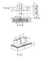
- FIGS. 1A, 1B and 1 Cshow the pattern layout and sections of the MOSFETS.
- an insulating layer 102On a semiconductor substrate 101 is formed an insulating layer 102 , which is in turn formed on top with a silicon fin layer 103 .
- a source 105 and a drain 106are formed over the silicon fin layer 103 on opposite sides thereof with an insulating film 104 interposed therebetween.
- An insulating film 108is formed on the source 105 and the drain 106 in order to insulate the source and the drain from a gate electrode 107 to be formed. Also, an insulating film 109 is formed on the sidewall of the groove between the source 105 and the drain 106 in order to insulate them from the gate electrode 107 .
- the gate electrode 107is formed in the groove.
- the implementation of this deviceinvolves the use of an expensive SOI substrate, which will increase the manufacturing cost of LSIs that are expected to be mass-produced.
- the device reliabilitymay be subject to the quality of the SOI substrate.
- a device adapted to perform the same operation as the device of SOI structure as illustrated in FIGS. 1A, 1B and 1 Ccan be implemented using a normal bulk substrate.
- the device based on a bulk substratehas a substrate projection which forms a device region and is implemented by selectively oxidizing the bottom of the device region.
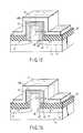
- FIG. 2is a perspective view of a conventional device using a bulk substrate and FIG. 3 is a cross-sectional view of the device.
- an insulating film 112is formed on a semiconductor substrate 111 .
- a source 113 and a drain 114are formed on the insulating film 112 .
- a gate electrode 116is formed over a semiconductor layer 110 between the source 113 and the drain 114 with a gate insulating film 115 interposed therebetween.
- FIGS. 4 and 5are sectional views of the MISFET in steps of manufacture thereof.
- a protruding region 121 Ais formed on a semiconductor substrate 121 .
- a gate insulating film 122is formed on the protruding region 121 A.
- An insulating film 123is formed on opposite sides of the protruding region 121 A.
- a mask material 124is formed on the insulating film 123 .
- the deviceis subjected to an ion implantation operation to prevent the occurrence of punch-through in deep portions of source and drain diffusion layers.
- This ion implantationallows a heavily doped region 125 to be formed at the bottom of the protruding region 121 A.
- shallow source and drain regions 126are formed in the top surface and the side surface of the protruding region 121 A, thereby allowing each of the top surface and the side surface to operate as an almost independent MISFET.
- the MISFET shown in FIGS. 4 and 5is not a device of the SOI structure; for the protruding region 121 A and the underlying semiconductor substrate 121 are joined together.
- the MISFEThas advantages that heat due to the Joule effect and the substrate floating effect are decreased.
- a semiconductor devicecomprising: a semiconductor projection having a semiconductor layer of a first conductivity type and side surfaces and a top surface, the semiconductor projection being formed on a semiconductor substrate of the first conductivity type; a gate electrode formed above at least the side surfaces of the semiconductor projection with a gate insulating film interposed therebetween; source and drain regions of a second conductivity type formed in the side surfaces of the semiconductor projection so that they are located on opposite sides of the gate electrode; first and second device isolation insulating films formed over the semiconductor substrate on opposite sides of the semiconductor projection; a first impurity region of the first conductivity type formed in a portion of the semiconductor substrate below the first device isolation insulating film; and a second impurity region of the first conductivity type formed in a portion of the semiconductor substrate below the second device isolation insulating film, the second impurity region being in contact with the first impurity region in a portion of the semiconductor substrate below the semiconductor projection.
- FIG. 1Ais a top view of a conventional MOSFET
- FIG. 1Bis a sectional view of the MOSFET taken along line 1 B- 1 B of FIG. 1A;
- FIG. 1Cis a sectional view of the MOSFET taken along line 1 C- 1 C of FIG. 1A;
- FIG. 2is a perspective view of another conventional MOSFET using a bulk substrate
- FIG. 3is a sectional view of the MOSFET of FIG. 2;
- FIGS. 4 and 5are sectional views of still another conventional MISFET in steps of manufacture
- FIG. 6is a perspective view of a semiconductor device according to a first embodiment of the present invention.
- FIG. 7is a perspective view of a semiconductor device according to a second embodiment of the present invention.
- FIG. 8is a perspective view of a semiconductor device according to a modification of the second embodiment of the present invention.
- FIG. 9is a perspective view of a semiconductor device according to another modification of the second embodiment of the present invention.
- FIG. 10is a perspective view of a semiconductor device according to a third embodiment of the present invention.
- FIG. 11Ais a top view of the semiconductor device of the third embodiment
- FIG. 11Bis a side view of the semiconductor device of the third embodiment
- FIG. 11Cis a sectional view taken along line 11 C- 11 C of FIG. 11A;
- FIG. 11Dis a sectional view taken along line 11 D- 11 D of FIG. 11A;
- FIG. 12is a perspective view of a portion of a semiconductor device according to a fourth embodiment of the present invention.
- FIG. 13is a perspective view of a portion of a semiconductor device according to a modification of the fourth embodiment of the present invention.
- FIG. 14is a perspective view of a semiconductor device according to a fifth embodiment of the present invention.
- FIGS. 15A to 15 Dare sectional views, in the order of steps of manufacture, of a semiconductor device according to a sixth embodiment of the present invention.
- FIGS. 16A to 16 Care plan views, in the order of steps of manufacture, of the semiconductor device according to the sixth embodiment of the present invention.
- FIG. 17is a perspective view of the semiconductor device according to the sixth embodiment of the present invention.
- MISFETMIS field effect transistor
- FIG. 6is a perspective view of a semiconductor device according to a first embodiment of the invention.
- a p-type silicon semiconductor substrate 11is processed to have a substrate projection 11 A.
- the projection 11 Aforms a device region. Portions of the substrate 11 on opposite sides of the projection 11 A form device isolation regions.
- a device isolation insulating film 12is formed on semiconductor substrate 11 in the device isolation regions.
- the projection 11 Ais 0.1 ⁇ m or less in thickness (corresponding to the thickness in the direction normal to the direction of the channel length) and 0.5 to 1.0 ⁇ m in height from the surface of the substrate 11 .
- the height of the projectionneed not be limited to 1.0 ⁇ m or less and may be more than 1.0 ⁇ m if the manufacturing technology permits.
- a gate insulating film 13is formed on top and side with the substrate projection 11 A. That is, the gate insulating film 13 is formed to cover the substrate projection 11 A.
- the gate insulating film 13consists of, for example, silicon oxide formed by thermal oxidation.
- a gate electrode 14is formed on a portion of the gate insulating film 13 that covers the projection 11 A. Also, the gate electrode 14 is formed on a portion of the device isolation insulating film 12 . After the gate electrode was formed, source diffusion layers 15 and drain diffusion layers 16 , which are opposite in conductivity type to the semiconductor substrate 11 , are formed in those portions of the side surfaces of the projection 11 A which are located on opposite sides of the gate electrode 14 . In the step of forming the source and drain regions, phosphorous (P) or arsenic (As) is introduced into the side surfaces of the projection except below the gate electrode by means of ion implantation. The ion implantation is carried out in a self-aligned manner using the gate electrode 14 as a mask.
- the source and drain regions 15 and 16are formed only in the side surfaces of the projection 11 A, they may also be formed in the top surface of the projection as required. In that case, contact can be made to interconnect layers via the drain and source regions formed in the top surface.
- Heavily doped regions 17 of p-type conductivityare formed in the substrate below the device isolation insulating film 12 and the substrate projection 11 A.
- the heavily doped regions 17are of the same conductivity type as the substrate. That is, the p + -type regions 17 formed by ion implantation in the semiconductor substrate 11 below the device isolation insulating film 12 on opposite sides of the substrate projection 11 A are joined together in the substrate below the projection.
- a contact plug 18is formed in the device isolation insulating film 12 to establish electrical connection between the semiconductor substrate 11 and an interconnect layer not shown. Since the p + -type regions 17 have been formed on top of the substrate 11 , ohmic contact can be obtained between the contact plug 18 and the substrate 11 without performing ion implantation anew at the time of forming the contact plug.
- the semiconductor device shown in FIG. 6serves the same function as the previously described conventional SOI substrate-based MISFET through the use of the bulk substrate.
- the gate electrode 14needs a contact area (not shown) for connection to an interconnect layer. For this reason, the gate electrode 14 is formed to overlap the substrate 11 in the device isolation region.
- the p + -type regions 17is formed in the substrate in the device isolation region including portions just below the gate electrode 14 by doping p-type impurities of opposite conductivity type to carriers in the channel.
- the device isolation insulating film 12 on the substrate in the device isolation regionis formed to be large in thickness, so that the insulating film that acts effectively as a gate insulating film in the overlapping portion of the gate electrode and the semiconductor substrate is made large in thickness. For this reason, the threshold voltage of the parasitic MISFET formed in the device isolation region can be increased, allowing the parasitic MISFET to be in the off state at all times.
- boron (B)is introduced into the device isolation region to form the p + -type impurity regions 17 .
- the thickness of the substrate projection 11 A(the thickness in the direction normal to the direction of the channel length) is smaller than the maximum width Wd of the depletion layer formed in the substrate projection 11 A when a voltage is applied to the gate electrode, then the entire substrate projection will be filled with the depletion layer at the time of operation.
- the MISFET of this embodimentperforms the same operation as a fully depleted SOI device. In this case, even if the doping level of the substrate projection 11 A is low, since potential control in the channel is performed by the gate electrode on the sidewalls of the projection, it is possible to control the short channel effect with ease in comparison with a planar MISFET of the conventional structure.
- the doping concentration of the substrate projection 11 Acan be set low, thus allowing the magnitude of electric field in the vertical direction produced by impurities in the substrate to be smaller than in normal planar MISFETs and the carrier mobility represented by a function of the vertical electric field to be larger than in the planar devices. Therefore, the MISFET of this embodiment provides higher current drivability than the planar devices even with the same operating voltage and the same gate width.
- the substrate projection 11 Acauses lateral diffusion of impurities which are ion implanted vertically into the semiconductor substrate 11 in the device isolation region, resulting in the substrate region below the projection 11 A being doped. That is, the p + -type doped regions 17 on opposite sides of the projection are joined together in the substrate region below the projection, so that the P + -type doped region is also formed below the projection.
- the device isolation characteristiccan be improved because not only the substrate region in the device isolation region but also the substrate region below the substrate projection 11 A can be doped with impurities. That is, the occurrence of punch-through can be prevented and the isolation between adjacent devices can be maintained.
- the transistor portion formed in the side surfaces of the substrate projectionis relatively effective in controlling the short channel effect.
- the reasonis that the thickness of the channel forming silicon layer is defined by the width of the substrate projection and the double-gate structure functions favorably.
- the transistor formed in the top surface of the substrate projectionis affected by the drain impurity diffusion layers formed in the side surfaces of the projection, so that the drain junction depth increases and the effective SOI film thickness in the vertical direction looks large.
- the second embodimentis intended to prevent the occurrence of punch-through between source and drain even with a very fine gate electrode formed by preventing the channel from being formed in the top surface of the substrate projection, i.e., by using only the side surfaces of the projection as the channel.
- the semiconductor device according to the second embodiment of the present inventionis basically characterized in that the top portion of the substrate projection is not used as the channel.
- FIGS. 7, 8 and 9Examples of structures such that no channel is formed in the top surface of the substrate projection are illustrated in FIGS. 7, 8 and 9 .
- the top surfaceis doped with impurities of opposite conductivity type to carriers in the channel.
- the gate oxide film formed on the top of the substrate projectionis made sufficiently large in thickness so as not to allow the channel to be formed under actually used operating voltages.
- the gate electrodeis formed so that it is not located on the top surface of the projection. Any combination of these three structures may be used.
- FIGS. 7, 8 and 9The structures shown in FIGS. 7, 8 and 9 will be described below in detail.
- FIG. 7is a perspective view of a semiconductor device according to the second embodiment.
- a region 21is formed in the upper portion of the substrate projection 11 A, as shown in FIG. 7.
- the region 21is doped with p-type impurities of opposite conductivity type to carriers in the channel. Otherwise, the device of FIG. 7 remains unchanged from the device of FIG. 6.
- the semiconductor device of such a structureis fabricated as follows: First, in forming the substrate projection 11 A, an insulating film as a cap film, such as a film of silicon nitride, is formed over the surface of the semiconductor substrate 11 and then patterned in the form of a strip. The semiconductor substrate is then subjected to reactive ion etching (RIE) using the silicon nitride film as a mask, whereby the substrate projection 11 A of a given width (thickness) and height is formed.
- RIEreactive ion etching
- impuritiesare introduced vertically into the top surface of the projection by means of ion implantation.
- boron (B)is implanted at 15 keV and at a dose of 5 ⁇ 10 13 cm ⁇ 2 or more.
- the gate insulating film 13is formed on the top surface and the side surfaces of the projection by means of thermal oxidation.
- a film of polysiliconis deposited onto the gate insulating film 13 and then patterned to form the gate electrode 14 .
- impurities of, for example, P or Asare introduced into the side surfaces of the projection 11 A except their portions below the gate electrode 14 by means of ion implantation, thereby forming the source and drain regions 15 and 16 .
- FIG. 8is a perspective view of a semiconductor device according to a modification of the second embodiment.
- An insulating film 22is formed on the substrate projection 11 A as shown in FIG. 8. It is recommended that as the insulating film 22 the cap film (for example, silicon nitride film) used in forming the substrate projection be used as it is. Alternatively, a silicon oxide film may be separately formed as the insulating film 22 . Otherwise, the device of FIG. 9 remains unchanged from the device of the first embodiment.
- the cap filmfor example, silicon nitride film
- the insulating film present between the gate electrode 14 and the top surface of the substrate projection 11 Acan be made sufficiently thick so as not to allow the channel to be formed under usually used operating voltages.
- the semiconductor device of such a structureis fabricated as follows: First, in forming the substrate projection 11 A, an insulating film as a cap film, such as a film of silicon nitride, is formed over the surface of the semiconductor substrate 11 and then patterned in the form of a strip. The semiconductor substrate is then subjected to reactive ion etching (RIE) using the silicon nitride film as a mask, whereby the substrate projection 11 A is formed.
- RIEreactive ion etching
- the gate insulating film 13consisting of silicon oxide is formed on the side surfaces of the projection by means of thermal oxidation with the insulating film 22 left.
- a film of polysiliconis deposited onto the gate insulating film 13 and the insulating film 22 and then patterned to form the gate electrode 14 .
- impuritiessuch as P or As, are introduced into the side surfaces of the projection 11 A except their respective portions below the gate electrode 14 by means of ion implantation, thereby forming the source and drain regions 15 and 16 .
- FIG. 9is a perspective view of a semiconductor device according to another modification of the second embodiment.
- gate electrodes 14 A and 14 Bare formed only on the sidewalls of the projection. That is, two gate electrodes 14 A and 14 B are formed on the sidewalls of the projection so as to sandwich the projection and self-align to each other.
- the two gate electrodesare arranged on a straight line perpendicular to the direction of the channel length. With this semiconductor device, the gate electrode is separated into two; thus, it is required to provide each of the two electrodes with a separate contact. Otherwise, the device of FIG. 9 remains unchanged from the device of the first embodiment.
- the semiconductor device thus constructedcan be used in the double-gate FET mode in which the same bias voltage is applied to the two gate electrodes 14 A and 14 B. It is also possible to apply a different voltage to each of the gate electrodes 14 A and 14 B.
- An example of applying a different voltage to each of the two gate electrodes 14 A and 14 Bis the backgate FET mode in which one of the two electrodes is supplied with a gate voltage for channel control and the other is supplied with a different voltage as the substrate potential.
- the device shown in FIG. 9is allowed to control the threshold voltage when used in the backgate FET mode.
- a plurality of semiconductor devices shown in FIG. 9can be used simultaneously, in which case modifications to the interconnections and the power supply system would allow some devices to operate in the double-gate FET mode and other devices to operate in the backgate FET mode.
- the semiconductor device of such a structure as shown in FIG. 9is fabricated as follows: First, in forming the substrate projection 11 A, an insulating film as a cap film, such as a film of silicon nitride, is formed over the surface of the semiconductor substrate 11 and then patterned in the form of a strip. The semiconductor substrate is then subjected to reactive ion etching using the silicon nitride film as a mask, whereby the substrate projection 11 A is formed.
- a cap filmsuch as a film of silicon nitride
- the gate insulating film 13consisting of silicon oxide is formed on the side surfaces of the projection by means of thermal oxidation with the silicon nitride film left.
- a film of polysiliconis deposited onto the gate insulating film 13 and the insulating film 22 and then patterned to form the gate electrode 14 .
- the polysilicon film present on the top of the projectionis removed by means of CMP or RIE. Moreover, the insulating film present on the top of the projection is removed. Furthermore, impurities, such as P or As, are introduced into the side surfaces of the projection 11 A except their respective portions below the gate electrode 14 by means of ion implantation, thereby forming the source and drain regions 15 and 16 .
- Each of the semiconductor devices of the second embodimentis allowed to perform the same operation as fully depleted MISFETs using the SOI substrate.
- the third embodimentis therefore intended to provide a MISFET which uses a thick substrate projection in which, as shown in FIGS. 10 and 11A to 11 D, the channel region and its neighborhood are made small in thickness, whereas the region in which the source and drain are to be formed are made large in thickness, thereby allowing the increase of the parasitic resistance to be minimized.
- FIG. 10is a perspective view of a semiconductor device according to the third embodiment.
- FIG. 11Ais a plan view of the semiconductor device.
- FIG. 11Bis a side view of the semiconductor device.
- FIG. 11Cis a cross-sectional view of the semiconductor device taken along line 11 C- 11 C of FIG. 11A.
- FIG. 11Dis a cross-sectional view of the semiconductor device taken along line 11 D- 11 D of FIG. 11A.
- FIGS. 10 and 11A to 11 Dare fabricated in the following way.
- the device geometrysomewhat varies according to the fabrication method.
- portions of a thick silicon substrate 11 around the region which is to form a projectionare etched away to form the substrate projection of 0.15-0.20 ⁇ m in width.
- the direction of the width of the projectionis parallel to the surface of the substrate 11 and normal to the direction from source to drain (i.e., the direction of the channel length).
- an insulating film of, for example, silicon nitrideis deposited which is to be used as a mask in forming the gate electrode.
- the silicon nitride filmis patterned using lithographic techniques to form a groove in that film.
- the semiconductor substrate 11is subjected to oxidation to form an oxide film of 50-100 nm in thickness, the oxide film comes to have a region which resembles a bird's beak as is well known in the LOCOS process. After that, by selectively removing the oxide film, the substrate projection 31 A is formed which is thick in the source and drain portions and thin in the channel portion and part of the diffusion portion near the channel.
- the gate insulating film 13is formed on the top surface and the side surfaces of that portion of the projection 31 A which is made thin in the gate electrode forming mask.
- a polysilicon filmis formed on the gate insulating film 13 in the gate electrode forming mask and the excess polysilicon film is polished by CMP to form the gate electrode 14 .
- the gate electrode forming mask material(the silicon nitride film) is removed.
- ion implantation or vapor phase dopingis performed on the side surfaces (source and drain formed portions) of the substrate projection except the channel region, thereby forming deep, low-resistivity source and drain diffused layers 15 and 16 .
- shallow junctionsare formed in the diffused portions near the channel region.
- the same structurecan also be formed by applying the elevated source/drain structure using epitaxial techniques after the formation of a transistor in the substrate projection.
- the source diffused layers 15 and the drain diffused layers 16are formed only in the side surfaces of the substrate projection 31 A, they may be formed in the top surface of the projection as required. In that case, contacts may be made to interconnect layers via the source and drain diffused layers 15 and 16 formed in the top surface.
- the fourth embodimentis therefore intended to provide a three-dimensional MISFET that performs the same operation as SOI devices by forming a substrate projection of a relatively large thickness of, for example, the order to 0.5 to 1.0 ⁇ m.
- the fourth embodimentis characterized by forming an intrinsic pillar as a substrate projection and then forming a stacked channel structure of stacked p + /n ⁇ /p ⁇ layers.
- FIG. 12is a perspective view of a portion of a semiconductor device of the fourth embodiment.
- FIG. 12shows particularly the channel portion, and the projection in which the source and drain diffused layers are formed is made large in thickness as illustrated in FIGS. 10 and 11A to 11 D.
- an insulating film as a cap filmsuch as a film of silicon nitride, is formed over the surface of a p-type semiconductor substrate 11 and then patterned into the shape of a strip.
- the semiconductor substrateis then subjected to reactive ion etching using the silicon nitride film as a mask, whereby an intrinsic pillar of a given width (thickness) and height is formed.
- a p + -type layer 42 , an n ⁇ -type layer 43 and a p ⁇ -type layer 44are formed in this order on the top surface and the side surfaces of the pillar, i.e., so as to surround the pillar, to form the substrate projection 41 A.
- a gate oxide film 13consisting of silicon oxide is formed on the side surfaces and the top surface of the substrate projection 41 A by means of thermal oxidation.
- a polysilicon filmis deposited on the gate insulating film 13 and then patterned to form a gate electrode 14 .
- FIG. 13is a perspective view of a portion of a semiconductor device according to a modification of the fourth embodiment.
- FIG. 13shows particularly the channel portion, and the projection in which the source and drain diffused layers are formed is made large in thickness as illustrated in FIGS. 10 and 11A to 11 D.
- an insulating film as a cap filmsuch as a film of silicon nitride, is formed over the surface of a p-type semiconductor substrate 11 and then patterned into the shape of a strip.
- the semiconductor substrateis then subjected to reactive ion etching using the silicon nitride film as a mask, whereby an intrinsic pillar of a given width and height is formed.
- impurities of, for example, boronare introduced into the device isolation region of the semiconductor substrate 11 through ion implantation to form p + -type doped regions 17 .
- the impuritiesare also introduced into the pillar to form a p + -type layer 42 .
- a device isolation insulating film 12 of, for example, silicon oxideis formed over the device isolation region of the semiconductor substrate 11 .
- n ⁇ -type layer 43 and a p ⁇ -type layer (channel layer) 44are grown over the p + -type layer 42 , thereby forming the substrate projection 41 B.
- the formation of the p + -type doped region 17 into the device isolation region of the semiconductor device 11is carried out when the pillar is still thin, that is, immediately after the pillar has been formed.
- the p-type impuritiesdiffuse to under the substrate projection, allowing the p + -type doped region 17 to come in contact with the innermost p + -type layer 42 of the pillar.
- the potential application to the p + -type doped region 17results in the potential application to the p + -type layer 42 of the substrate projection 41 B, allowing the device to operate as a four-terminal device.
- the center pillar of the substrate projection 41 A or 41 Bcan be formed to any thickness.
- the thickness of the pillarcan be set so that the substrate can be processed easily to form the substrate projection with the same structure as thin-film SOI devices.
- the difficulties involved in fabricating the devicecan be decreased.
- FIGS. 12 and 13depict, in enlarged view, only the channel portion just below the gate.
- the source and drainit is required that their respective diffused layers be not in contact with the n ⁇ -type layer 43 .
- Such elevated source/drain structures using selective epitaxial growth as used in the device shown in FIGS. 10 and 11A to 11 D or halo structures (pocket structures)are recommended.
- the use of these structuresallows easy prevention of the source and drain diffused layers (n + -type layers) from coming into contact with the n-type layer 43 and the channel structures shown in FIGS. 12 and 13 to be implemented.
- the fourth embodimenthas been described in terms of an n-channel field effect transistor, the principles of the invention can be applied to a p-channel field effect transistor by reversing the conductivity type of impurities. By performing doping of the well and the channel separately and optimizing the halo structure, devices equivalent to high-performance CMOS SOI devices can be implemented.
- the actual thickness of polysilicon that can be depositedis at most 200 nm, and a step of about 800 nm is created between the top of the substrate projection and the top of the gate electrode.
- a step of about 800 nmis created between the top of the substrate projection and the top of the gate electrode.
- the fifth embodimentis therefore intended to provide a three-dimensional MISFET in which the gate electrode is shaped as shown in FIG. 14 and the difference in level between the source and drain contact areas on the substrate projection and the gate contact areas is less than 200 nm.
- FIG. 14is a perspective view of a semiconductor device of the fifth embodiment.
- portions of the p-type silicon substrate 11 around the region which is to form a projectionare etched to form the substrate projection of about 2 ⁇ m in width.
- the direction of the width of the projectionis parallel to the surface of the substrate 11 and normal to the direction from source to drain (i.e., the direction of the channel length).
- an insulating film of, for example, silicon nitrideis deposited which is to be used as a mask in forming the gate electrode.
- the silicon nitride filmis etched using lithographic and RIE techniques to form a groove in that film.
- the semiconductor substrate 11is subjected to oxidation to form an oxide film of 50-100 nm in thickness, in which case the oxide film comes to have a region which resembles a bird's beak as is well known in the LOCOS process. After that, by selectively removing the oxide film, a substrate projection 51 A is formed which is thick in the source and drain portions and thin in the channel portion and part of the diffusion portion near the channel.
- the gate insulating film 13is formed on the top surface and the side surfaces of that portion of the projection 51 A within the gate electrode forming mask.
- a polysilicon filmis buried in the gate electrode forming mask and the excess polysilicon film is polished by CMP to form the gate electrode 54 .
- the gate electrode 54can be formed to such a height as shown in FIG. 14. Thus, the difference in level between the contacts on the gate electrode 54 and the contacts on the source and drain diffusion layers 15 and 16 can be reduced.
- the aspect ratio of the contact holescan be reduced and the contact holes can be formed simultaneously on the gate electrode 54 and the source and drain diffused layers 15 and 16 . Also, the parasitic resistance associated with the gate electrode 54 can be reduced because the thickness of the polysilicon film is large.
- the sixth embodimentprovides a semiconductor device in which the substrate projection is formed by epitaxial growth and the formation of contacts to the source and drain diffused layers is easy.
- FIGS. 15A to 15 Dare sectional views, in the order of steps of manufacture, of the semiconductor device of the sixth embodiment.
- FIGS. 16A to 16 Care plan views, in the order of steps of manufacture, of the semiconductor device.
- an insulating film 62is formed on a semiconductor substrate 61 .
- the insulating film 62is patterned to form an opening 63 in the region where the channel of a MISFET is to be formed.
- the plan view of the structure at this stageis illustrated in FIG. 16A.
- the epitaxial layer 64is patterned by means of lithographic and dry etching techniques to form a substrate projection 64 A where the source, the drain and the channel are to be formed.
- the plan view of the structure at this stageis illustrated in FIG. 16B. In this figure, the upper and lower portions where the source and drain diffused regions are to be formed are made larger in width than the central portion where the channel is to be formed.
- a gate insulating film 65is formed on the top surface and side surfaces of the substrate projection 64 A.
- a gate electrode materialis deposited on the gate insulating film 65 and then patterned by lithographic and dry etching techniques to form a gate electrode 66 .
- phosphorous (p) or arsenic (As)is introduced into the portions of the substrate projection 64 A except below the gate electrode to form the source and drain diffused layers 67 and 68 .
- FIG. 16CThe plan view of the structure at this point is illustrated in FIG. 16C.
- the perspective view of the semiconductor device thus fabricatedis illustrated in FIG. 17.
- the semiconductor device shown in FIG. 17insulation of the source and drain regions of a MISFET called the delta or fin type from the substrate can be obtained. As a result, even if the device-to-device spacing is reduced, there is little possibility of erroneous conduction between adjacent devices and hence the device isolation characteristic can be improved.
- the channel portionis formed of the epitaxial layer 64 grown from the semiconductor substrate 61 ; thus, the bias to the channel can be controlled from the side of the semiconductor substrate 61 .
- the length in the direction perpendicular to the direction of the channel length of the portions of the substrate projection in which the source and drain regions are formedis made larger than the corresponding length of the central portion where the channel is formed.
- the length in the direction parallel to the surface of the substrate and perpendicular to the direction from source to drain of that portion of the substrate projection on which the gate electrode is locatedis made shorter than the length in the corresponding direction of those portions of the substrate projection where the source and drain regions are formed.
- the channelis electrically connected with the substrate, a bias can be applied to the substrate, allowing threshold voltage control to be performed and the substrate floating effect to be reduced.
- the channel and the source and drain regionsare formed from monocrystalline silicon, allowing the parasitic resistance to be reduced.
- p-channel MIS field effect transistorscan also be fabricated simply by changing the conductivity type using suitable process conditions.
- semiconductor devicescan be provided which are allowed to operate as fully depleted devices even if the gate length is very short and can reduce heat resulting from the Joule effect and the substrate floating effect.
Landscapes
- Insulated Gate Type Field-Effect Transistor (AREA)
- Thin Film Transistor (AREA)
Abstract
Description
- This application is based upon and claims the benefit of priority from the prior Japanese Patent Application No. 2000-297672, filed Sep. 28, 2000, the entire contents of which are incorporated herein by reference.[0001]
- 1. Field of the Invention[0002]
- This invention relates to a semiconductor device and more specifically to a MIS field effect transistor (MISFET) of three-dimensional structure.[0003]
- 2. Description of the Related Art[0004]
- There have been proposals for double-gate fully depleted-SOI MOSFETs which are one type of MISFETs of three-dimensional structure (D. Hisamoto et al. :IEDM 1998 P.1032, X. Huang et al. :IEDM 1999 P.67, Jpn. Pat. Appln. KOKAI Publication No. 2-263473, and Japanese Examined Patent Application No. 2768719). The double-gate fully depleted-SOI MOSFET comprises a SOI (Silicon on Insulator) substrate, a single-crystal silicon strip, and a gate electrode. The single-crystal silicon strip has been made by etching the uppermost layer of the SOI substrate, i.e., a single-crystal silicon layer. The gate electrode lies above the the silicon strip and extends across the silicon strip. The upper surface region and side regions of the strip serve as the channel.[0005]
- The above MOSFETs provide high current drivability, are more economical of space in the direction of gate width than conventional MOSFETS, and have the short-channel effect controlled. They are therefore promising for devices used in future LSIs.[0006]
- FIGS. 1A, 1B and[0007]1C show the pattern layout and sections of the MOSFETS. On a
semiconductor substrate 101 is formed aninsulating layer 102, which is in turn formed on top with asilicon fin layer 103. Asource 105 and adrain 106 are formed over thesilicon fin layer 103 on opposite sides thereof with aninsulating film 104 interposed therebetween. - An[0008]
insulating film 108 is formed on thesource 105 and thedrain 106 in order to insulate the source and the drain from agate electrode 107 to be formed. Also, aninsulating film 109 is formed on the sidewall of the groove between thesource 105 and thedrain 106 in order to insulate them from thegate electrode 107. Thegate electrode 107 is formed in the groove. - The implementation of this device involves the use of an expensive SOI substrate, which will increase the manufacturing cost of LSIs that are expected to be mass-produced. In addition, the device reliability may be subject to the quality of the SOI substrate.[0009]
- A device adapted to perform the same operation as the device of SOI structure as illustrated in FIGS. 1A, 1B and[0010]1C can be implemented using a normal bulk substrate. The device based on a bulk substrate has a substrate projection which forms a device region and is implemented by selectively oxidizing the bottom of the device region.
- FIG. 2 is a perspective view of a conventional device using a bulk substrate and FIG. 3 is a cross-sectional view of the device. As shown in FIGS. 2 and 3, an[0011]
insulating film 112 is formed on asemiconductor substrate 111. Asource 113 and adrain 114 are formed on theinsulating film 112. Agate electrode 116 is formed over asemiconductor layer 110 between thesource 113 and thedrain 114 with agate insulating film 115 interposed therebetween. - With the device shown in FIGS. 2 and 3, however, a decrease in the size of the device region may make it difficult to control the thickness of the oxide film and may cause deformation due to thermal oxidation at high temperatures to affect the device performance[0012]
- With respect to the SOI structure in the aforementioned two devices, it is known that, since the thermal conductivity of the insulating file existing under the silicon layer is lower than that of crystal silicon, self-heating occurs due to Joule heat generated by drain current to cause a degradation in the drain current. Therefore, the devices shown in FIGS. 1A to[0013]1C and FIGS. 2 and 3 cannot necessarily display the performance fully for application to LSIs.
- In devices of the SOI structure, holes generated by impact ionization in the channel have their escape cut off and are trapped in the lower portion of the channel, causing the so-called substrate floating effect. This phenomenon is remarkably observed particularly in n-channel field effect transistors. For this reason, there is fear that the substrate floating effect might affect the operation of high-speed switching devices in particular.[0014]
- An example of a MISFET that is allowed to have a three-dimensional structure through the use of a bulk substrate is one illustrated in U.S. Pat. No. 5844278. With this MISFET, the bulk substrate is processed to have a projection shape and the substrate projection shape is made to have such a gate electrode structure as in the aforementioned prior art.[0015]
- FIGS. 4 and 5 are sectional views of the MISFET in steps of manufacture thereof.[0016]
- As shown in FIG. 4, a[0017]
protruding region 121A is formed on asemiconductor substrate 121. Agate insulating film 122 is formed on theprotruding region 121A. Aninsulating film 123 is formed on opposite sides of theprotruding region 121A. Amask material 124 is formed on theinsulating film 123. - In the structure of FIG. 4, the device is subjected to an ion implantation operation to prevent the occurrence of punch-through in deep portions of source and drain diffusion layers. This ion implantation allows a heavily[0018]
doped region 125 to be formed at the bottom of theprotruding region 121A. - Furthermore, as shown in FIG. 5, shallow source and[0019]
drain regions 126 are formed in the top surface and the side surface of theprotruding region 121A, thereby allowing each of the top surface and the side surface to operate as an almost independent MISFET. - The MISFET shown in FIGS. 4 and 5 is not a device of the SOI structure; for the[0020]
protruding region 121A and theunderlying semiconductor substrate 121 are joined together. Thus, the MISFET has advantages that heat due to the Joule effect and the substrate floating effect are decreased. - However, trying to reduce the gate length (for example, 0.1 μm or less) and operate the device as a completely depleted one makes difficult the process of manufacturing the structure shown in FIGS. 4 and 5. Thus, the demand has increased for developing a structure having a novel structure adapted for the generation of devices in which the gate length is 0.1 μm or less.[0021]
- According to an aspect of the present invention, there is provided a semiconductor device comprising: a semiconductor projection having a semiconductor layer of a first conductivity type and side surfaces and a top surface, the semiconductor projection being formed on a semiconductor substrate of the first conductivity type; a gate electrode formed above at least the side surfaces of the semiconductor projection with a gate insulating film interposed therebetween; source and drain regions of a second conductivity type formed in the side surfaces of the semiconductor projection so that they are located on opposite sides of the gate electrode; first and second device isolation insulating films formed over the semiconductor substrate on opposite sides of the semiconductor projection; a first impurity region of the first conductivity type formed in a portion of the semiconductor substrate below the first device isolation insulating film; and a second impurity region of the first conductivity type formed in a portion of the semiconductor substrate below the second device isolation insulating film, the second impurity region being in contact with the first impurity region in a portion of the semiconductor substrate below the semiconductor projection.[0022]
- FIG. 1A is a top view of a conventional MOSFET;[0023]
- FIG. 1B is a sectional view of the MOSFET taken along[0024]
line 1B-1B of FIG. 1A; - FIG. 1C is a sectional view of the MOSFET taken along[0025]
line 1C-1C of FIG. 1A; - FIG. 2 is a perspective view of another conventional MOSFET using a bulk substrate;[0026]
- FIG. 3 is a sectional view of the MOSFET of FIG. 2;[0027]
- FIGS. 4 and 5 are sectional views of still another conventional MISFET in steps of manufacture;[0028]
- FIG. 6 is a perspective view of a semiconductor device according to a first embodiment of the present invention;[0029]
- FIG. 7 is a perspective view of a semiconductor device according to a second embodiment of the present invention;[0030]
- FIG. 8 is a perspective view of a semiconductor device according to a modification of the second embodiment of the present invention;[0031]
- FIG. 9 is a perspective view of a semiconductor device according to another modification of the second embodiment of the present invention;[0032]
- FIG. 10 is a perspective view of a semiconductor device according to a third embodiment of the present invention;[0033]
- FIG. 11A is a top view of the semiconductor device of the third embodiment;[0034]
- FIG. 11B is a side view of the semiconductor device of the third embodiment;[0035]
- FIG. 11C is a sectional view taken along[0036]
line 11C-11C of FIG. 11A; - FIG. 11D is a sectional view taken along[0037]
line 11D-11D of FIG. 11A; - FIG. 12 is a perspective view of a portion of a semiconductor device according to a fourth embodiment of the present invention;[0038]
- FIG. 13 is a perspective view of a portion of a semiconductor device according to a modification of the fourth embodiment of the present invention;[0039]
- FIG. 14 is a perspective view of a semiconductor device according to a fifth embodiment of the present invention;[0040]
- FIGS. 15A to[0041]15D are sectional views, in the order of steps of manufacture, of a semiconductor device according to a sixth embodiment of the present invention;
- FIGS. 16A to[0042]16C are plan views, in the order of steps of manufacture, of the semiconductor device according to the sixth embodiment of the present invention; and
- FIG. 17 is a perspective view of the semiconductor device according to the sixth embodiment of the present invention.[0043]
- With reference to the accompanying drawings, a semiconductor device embodying the invention will be described in terms of a MIS field effect transistor (MISFET) of the three-dimensional structure.[0044]
- FIG. 6 is a perspective view of a semiconductor device according to a first embodiment of the invention.[0045]
- As shown in FIG. 6, a p-type[0046]
silicon semiconductor substrate 11 is processed to have asubstrate projection 11A. Theprojection 11A forms a device region. Portions of thesubstrate 11 on opposite sides of theprojection 11A form device isolation regions. A deviceisolation insulating film 12 is formed onsemiconductor substrate 11 in the device isolation regions. Here, theprojection 11A is 0.1 μm or less in thickness (corresponding to the thickness in the direction normal to the direction of the channel length) and 0.5 to 1.0 μm in height from the surface of thesubstrate 11. The height of the projection need not be limited to 1.0 μm or less and may be more than 1.0 μm if the manufacturing technology permits. - A[0047]
gate insulating film 13 is formed on top and side with thesubstrate projection 11A. That is, thegate insulating film 13 is formed to cover thesubstrate projection 11A. Thegate insulating film 13 consists of, for example, silicon oxide formed by thermal oxidation. - A[0048]
gate electrode 14 is formed on a portion of thegate insulating film 13 that covers theprojection 11A. Also, thegate electrode 14 is formed on a portion of the deviceisolation insulating film 12. After the gate electrode was formed, source diffusion layers15 and drain diffusion layers16, which are opposite in conductivity type to thesemiconductor substrate 11, are formed in those portions of the side surfaces of theprojection 11A which are located on opposite sides of thegate electrode 14. In the step of forming the source and drain regions, phosphorous (P) or arsenic (As) is introduced into the side surfaces of the projection except below the gate electrode by means of ion implantation. The ion implantation is carried out in a self-aligned manner using thegate electrode 14 as a mask. - Although, in the above description, the source and drain[0049]
regions projection 11A, they may also be formed in the top surface of the projection as required. In that case, contact can be made to interconnect layers via the drain and source regions formed in the top surface. - Heavily doped[0050]
regions 17 of p-type conductivity are formed in the substrate below the deviceisolation insulating film 12 and thesubstrate projection 11A. The heavily dopedregions 17 are of the same conductivity type as the substrate. That is, the p+-type regions 17 formed by ion implantation in thesemiconductor substrate 11 below the deviceisolation insulating film 12 on opposite sides of thesubstrate projection 11A are joined together in the substrate below the projection. - A[0051]
contact plug 18 is formed in the deviceisolation insulating film 12 to establish electrical connection between thesemiconductor substrate 11 and an interconnect layer not shown. Since the p+-type regions 17 have been formed on top of thesubstrate 11, ohmic contact can be obtained between thecontact plug 18 and thesubstrate 11 without performing ion implantation anew at the time of forming the contact plug. - The semiconductor device shown in FIG. 6 serves the same function as the previously described conventional SOI substrate-based MISFET through the use of the bulk substrate. The[0052]
gate electrode 14 needs a contact area (not shown) for connection to an interconnect layer. For this reason, thegate electrode 14 is formed to overlap thesubstrate 11 in the device isolation region. - With the semiconductor device, in order to maintain device-to-device isolation, it is required to control the short channel effect caused by a parasitic MISFET and to cause the parasitic MISFET in the overlapping portion of the gate electrode and the semiconductor substrate in the device isolation region to turn off at all times under actually used operating voltages.[0053]
- In this embodiment, therefore, the p[0054]+-
type regions 17 is formed in the substrate in the device isolation region including portions just below thegate electrode 14 by doping p-type impurities of opposite conductivity type to carriers in the channel. Further, the deviceisolation insulating film 12 on the substrate in the device isolation region is formed to be large in thickness, so that the insulating film that acts effectively as a gate insulating film in the overlapping portion of the gate electrode and the semiconductor substrate is made large in thickness. For this reason, the threshold voltage of the parasitic MISFET formed in the device isolation region can be increased, allowing the parasitic MISFET to be in the off state at all times. For example, to form an n-channel MISFET, boron (B) is introduced into the device isolation region to form the p+-type impurity regions 17. - If the thickness of the[0055]
substrate projection 11A (the thickness in the direction normal to the direction of the channel length) is smaller than the maximum width Wd of the depletion layer formed in thesubstrate projection 11A when a voltage is applied to the gate electrode, then the entire substrate projection will be filled with the depletion layer at the time of operation. Thus, the MISFET of this embodiment performs the same operation as a fully depleted SOI device. In this case, even if the doping level of thesubstrate projection 11A is low, since potential control in the channel is performed by the gate electrode on the sidewalls of the projection, it is possible to control the short channel effect with ease in comparison with a planar MISFET of the conventional structure. - For the same operation as the SOI device, the doping concentration of the[0056]
substrate projection 11A can be set low, thus allowing the magnitude of electric field in the vertical direction produced by impurities in the substrate to be smaller than in normal planar MISFETs and the carrier mobility represented by a function of the vertical electric field to be larger than in the planar devices. Therefore, the MISFET of this embodiment provides higher current drivability than the planar devices even with the same operating voltage and the same gate width. - Decreasing the thickness of the[0057]
substrate projection 11A causes lateral diffusion of impurities which are ion implanted vertically into thesemiconductor substrate 11 in the device isolation region, resulting in the substrate region below theprojection 11A being doped. That is, the p+-type dopedregions 17 on opposite sides of the projection are joined together in the substrate region below the projection, so that the P+-type doped region is also formed below the projection. With the semiconductor device of this embodiment, therefore, the device isolation characteristic can be improved because not only the substrate region in the device isolation region but also the substrate region below thesubstrate projection 11A can be doped with impurities. That is, the occurrence of punch-through can be prevented and the isolation between adjacent devices can be maintained. - In the semiconductor device of this embodiment which performs the same operation as fully depleted SOI devices, since its channel region is not isolated from the underlying semiconductor substrate by an insulating film low in thermal conductivity, the heat conduction characteristic can be improved, allowing a degradation in current caused by heat due to the Joule effect to be minimized.[0058]
- Second Embodiment[0059]
- In general, in the case of MISFETs using the SOI substrate, when a device that is very short in channel length is formed with the doping concentration of the substrate reduced, there is the possibility that punch-through occurs between source and drain as a result of extension of the depletion layer from the drain side. In order to control the short channel effect, the extension of the depletion layer must be controlled.[0060]
- With conventional fully-depleted planar MISFETs using the SOI substrate, the occurrence of punch-through is controlled by making the channel forming silicon layer very thin. When the gate length is reduced to 100 nm or less, the silicon layer must be made much smaller in thickness than the gate length, which increases the difficulty in fabricating devices.[0061]
- Consider here the case where, in the device of FIG. 6, the substrate projection is made large in height and the channel width is made large so as to increase effectively the area in which current flows.[0062]
- In this case, the transistor portion formed in the side surfaces of the substrate projection, as a thin-film device that performs the same operation as SOI devices, is relatively effective in controlling the short channel effect. The reason is that the thickness of the channel forming silicon layer is defined by the width of the substrate projection and the double-gate structure functions favorably.[0063]
- The transistor formed in the top surface of the substrate projection is affected by the drain impurity diffusion layers formed in the side surfaces of the projection, so that the drain junction depth increases and the effective SOI film thickness in the vertical direction looks large.[0064]
- As a result, depending on the source/drain structure, the extension of the depletion layer on the drain side increases, making punch-through between source and drain easy to occur. This is prominent particularly in the case where the substrate projection is 0.1 μm or more in height. For this reason, trying to increase the apparent current drivability by increasing the height of the substrate projection for compensation of the channel width results in increased possibility of punch-through.[0065]
- It is the prior art shown in FIG. 4 that is intended to remedy this drawback by optimizing the substrate doping profile. In this case as well, however, increasing the gate width, i.e., increasing the height of the substrate projection, results in difficulty in doping the entire region in which punch-through can occur with impurities. The effective upper limit of the gate width is determined by the range of depth to which impurities can be doped by the ion implantation technology.[0066]
- The second embodiment is intended to prevent the occurrence of punch-through between source and drain even with a very fine gate electrode formed by preventing the channel from being formed in the top surface of the substrate projection, i.e., by using only the side surfaces of the projection as the channel. Unlike the prior art, the semiconductor device according to the second embodiment of the present invention is basically characterized in that the top portion of the substrate projection is not used as the channel.[0067]
- Examples of structures such that no channel is formed in the top surface of the substrate projection are illustrated in FIGS. 7, 8 and[0068]9. In the example of FIG. 7, the top surface is doped with impurities of opposite conductivity type to carriers in the channel. In the example of FIG. 8, the gate oxide film formed on the top of the substrate projection is made sufficiently large in thickness so as not to allow the channel to be formed under actually used operating voltages. In the example of FIG. 9, the gate electrode is formed so that it is not located on the top surface of the projection. Any combination of these three structures may be used.
- The structures shown in FIGS. 7, 8 and[0069]9 will be described below in detail.
- FIG. 7 is a perspective view of a semiconductor device according to the second embodiment.[0070]
- A[0071]
region 21 is formed in the upper portion of thesubstrate projection 11A, as shown in FIG. 7. Theregion 21 is doped with p-type impurities of opposite conductivity type to carriers in the channel. Otherwise, the device of FIG. 7 remains unchanged from the device of FIG. 6. - The semiconductor device of such a structure is fabricated as follows: First, in forming the[0072]
substrate projection 11A, an insulating film as a cap film, such as a film of silicon nitride, is formed over the surface of thesemiconductor substrate 11 and then patterned in the form of a strip. The semiconductor substrate is then subjected to reactive ion etching (RIE) using the silicon nitride film as a mask, whereby thesubstrate projection 11A of a given width (thickness) and height is formed. - After the formation of the projection, impurities are introduced vertically into the top surface of the projection by means of ion implantation. For an n-channel MISFET as in this embodiment, boron (B) is implanted at 15 keV and at a dose of 5×10[0073]13cm−2or more.
- Subsequently, the[0074]
gate insulating film 13 is formed on the top surface and the side surfaces of the projection by means of thermal oxidation. A film of polysilicon is deposited onto thegate insulating film 13 and then patterned to form thegate electrode 14. - Moreover, impurities of, for example, P or As are introduced into the side surfaces of the[0075]
projection 11A except their portions below thegate electrode 14 by means of ion implantation, thereby forming the source and drainregions - FIG. 8 is a perspective view of a semiconductor device according to a modification of the second embodiment.[0076]
- An insulating[0077]
film 22 is formed on thesubstrate projection 11A as shown in FIG. 8. It is recommended that as the insulatingfilm 22 the cap film (for example, silicon nitride film) used in forming the substrate projection be used as it is. Alternatively, a silicon oxide film may be separately formed as the insulatingfilm 22. Otherwise, the device of FIG. 9 remains unchanged from the device of the first embodiment. - With the semiconductor device thus constructed, the insulating film present between the[0078]
gate electrode 14 and the top surface of thesubstrate projection 11A can be made sufficiently thick so as not to allow the channel to be formed under usually used operating voltages. - The semiconductor device of such a structure is fabricated as follows: First, in forming the[0079]
substrate projection 11A, an insulating film as a cap film, such as a film of silicon nitride, is formed over the surface of thesemiconductor substrate 11 and then patterned in the form of a strip. The semiconductor substrate is then subjected to reactive ion etching (RIE) using the silicon nitride film as a mask, whereby thesubstrate projection 11A is formed. - Subsequently, the[0080]
gate insulating film 13 consisting of silicon oxide is formed on the side surfaces of the projection by means of thermal oxidation with the insulatingfilm 22 left. A film of polysilicon is deposited onto thegate insulating film 13 and the insulatingfilm 22 and then patterned to form thegate electrode 14. - Moreover, impurities, such as P or As, are introduced into the side surfaces of the[0081]
projection 11A except their respective portions below thegate electrode 14 by means of ion implantation, thereby forming the source and drainregions - FIG. 9 is a perspective view of a semiconductor device according to another modification of the second embodiment.[0082]
- As shown in FIG. 9, no gate electrode is formed on top of the[0083]
projection 11A, butgate electrodes gate electrodes - The semiconductor device thus constructed can be used in the double-gate FET mode in which the same bias voltage is applied to the two[0084]
gate electrodes gate electrodes - An example of applying a different voltage to each of the two[0085]
gate electrodes - A plurality of semiconductor devices shown in FIG. 9 can be used simultaneously, in which case modifications to the interconnections and the power supply system would allow some devices to operate in the double-gate FET mode and other devices to operate in the backgate FET mode.[0086]
- The semiconductor device of such a structure as shown in FIG. 9 is fabricated as follows: First, in forming the[0087]
substrate projection 11A, an insulating film as a cap film, such as a film of silicon nitride, is formed over the surface of thesemiconductor substrate 11 and then patterned in the form of a strip. The semiconductor substrate is then subjected to reactive ion etching using the silicon nitride film as a mask, whereby thesubstrate projection 11A is formed. - Subsequently, the[0088]
gate insulating film 13 consisting of silicon oxide is formed on the side surfaces of the projection by means of thermal oxidation with the silicon nitride film left. A film of polysilicon is deposited onto thegate insulating film 13 and the insulatingfilm 22 and then patterned to form thegate electrode 14. - After that, the polysilicon film present on the top of the projection is removed by means of CMP or RIE. Moreover, the insulating film present on the top of the projection is removed. Furthermore, impurities, such as P or As, are introduced into the side surfaces of the[0089]
projection 11A except their respective portions below thegate electrode 14 by means of ion implantation, thereby forming the source and drainregions - In this case, it is possible to form a self-aligned double-gate MISFET that performs the same operation as an SOI device.[0090]
- Each of the semiconductor devices of the second embodiment is allowed to perform the same operation as fully depleted MISFETs using the SOI substrate.[0091]
- The structure to prevent the channel from being formed in the upper portion of the[0092]
substrate projection 11A will not provide a very serious damage under conditions that the width of thesubstrate projection 11A must be made small and the height of the projection must be set to 1 μm or more to obtain current drivability. If anything, it is apparent that the feature of the present invention of not using the top surface (upper portion) of the substrate projection for the channel provides effective means for controlling the short channel effect. - In the case of transistor operation using only the side surfaces of the substrate projection, in order to increase carrier mobility, it is required in the case of silicon that the side surface of the projection be parallel to the (100 ) plane and the channel be oriented in the direction of [100].[0093]
- Third Embodiment[0094]
- With the conventional three-dimensional MISFET shown in FIGS. 1A to[0095]1C and FIG. 2, in order to implement a fully depleted SOI device, it is required to make the thickness of the channel region small. If the thickness is 50 nm or less, it is advantageous to the formation of shallow junctions for source and drain regions. On the other hand, the source and drain regions becomes very thin in comparison with conventional planar MISFETs. For this reason, parasitic resistance associated with the source and drain regions becomes high. As a result, there will be a degradation in current drivability.
- The third embodiment is therefore intended to provide a MISFET which uses a thick substrate projection in which, as shown in FIGS. 10 and 11A to[0096]11D, the channel region and its neighborhood are made small in thickness, whereas the region in which the source and drain are to be formed are made large in thickness, thereby allowing the increase of the parasitic resistance to be minimized.
- FIG. 10 is a perspective view of a semiconductor device according to the third embodiment. FIG. 11A is a plan view of the semiconductor device. FIG. 11B is a side view of the semiconductor device. FIG. 11C is a cross-sectional view of the semiconductor device taken along[0097]
line 11C-11C of FIG. 11A. FIG. 11D is a cross-sectional view of the semiconductor device taken alongline 11D-11D of FIG. 11A. - The semiconductor device shown in FIGS. 10 and 11A to[0098]11D are fabricated in the following way. The device geometry somewhat varies according to the fabrication method.
- First, portions of a[0099]
thick silicon substrate 11 around the region which is to form a projection are etched away to form the substrate projection of 0.15-0.20 μm in width. The direction of the width of the projection is parallel to the surface of thesubstrate 11 and normal to the direction from source to drain (i.e., the direction of the channel length). Next, an insulating film of, for example, silicon nitride is deposited which is to be used as a mask in forming the gate electrode. The silicon nitride film is patterned using lithographic techniques to form a groove in that film. - The[0100]
semiconductor substrate 11 is subjected to oxidation to form an oxide film of 50-100 nm in thickness, the oxide film comes to have a region which resembles a bird's beak as is well known in the LOCOS process. After that, by selectively removing the oxide film, thesubstrate projection 31A is formed which is thick in the source and drain portions and thin in the channel portion and part of the diffusion portion near the channel. - After that, the[0101]
gate insulating film 13 is formed on the top surface and the side surfaces of that portion of theprojection 31A which is made thin in the gate electrode forming mask. A polysilicon film is formed on thegate insulating film 13 in the gate electrode forming mask and the excess polysilicon film is polished by CMP to form thegate electrode 14. - Next, the gate electrode forming mask material (the silicon nitride film) is removed. After that, ion implantation or vapor phase doping is performed on the side surfaces (source and drain formed portions) of the substrate projection except the channel region, thereby forming deep, low-resistivity source and drain diffused[0102]
layers - Although, in this embodiment, the source diffused layers[0103]15 and the drain diffused
layers 16 are formed only in the side surfaces of thesubstrate projection 31A, they may be formed in the top surface of the projection as required. In that case, contacts may be made to interconnect layers via the source and drain diffusedlayers - Fourth Embodiment[0104]
- As described previously, in order to make a MISFET that performs the same operation as SOI devices having a very fine gate regardless of whether it is of the conventional type or the three-dimension type, it is required to form the channel portion from a very thin silicon layer. Depending on circumstances, however, the structures described so far are expected to make it very difficult to process semiconductor substrates through lithographic and RIE techniques in particular.[0105]
- The fourth embodiment is therefore intended to provide a three-dimensional MISFET that performs the same operation as SOI devices by forming a substrate projection of a relatively large thickness of, for example, the order to 0.5 to 1.0 μm. The fourth embodiment is characterized by forming an intrinsic pillar as a substrate projection and then forming a stacked channel structure of stacked p[0106]+/n−/p−layers.
- FIG. 12 is a perspective view of a portion of a semiconductor device of the fourth embodiment. FIG. 12 shows particularly the channel portion, and the projection in which the source and drain diffused layers are formed is made large in thickness as illustrated in FIGS. 10 and 11A to[0107]11D.
- First, to form a[0108]
substrate projection 41A, an insulating film as a cap film, such as a film of silicon nitride, is formed over the surface of a p-type semiconductor substrate 11 and then patterned into the shape of a strip. The semiconductor substrate is then subjected to reactive ion etching using the silicon nitride film as a mask, whereby an intrinsic pillar of a given width (thickness) and height is formed. A p+-type layer 42, an n−-type layer 43 and a p−-type layer 44 are formed in this order on the top surface and the side surfaces of the pillar, i.e., so as to surround the pillar, to form thesubstrate projection 41A. - Next, a[0109]
gate oxide film 13 consisting of silicon oxide is formed on the side surfaces and the top surface of thesubstrate projection 41A by means of thermal oxidation. A polysilicon film is deposited on thegate insulating film 13 and then patterned to form agate electrode 14. - FIG. 13 is a perspective view of a portion of a semiconductor device according to a modification of the fourth embodiment. FIG. 13 shows particularly the channel portion, and the projection in which the source and drain diffused layers are formed is made large in thickness as illustrated in FIGS. 10 and 11A to[0110]11D.
- First, to form a[0111]
substrate projection 41B, an insulating film as a cap film, such as a film of silicon nitride, is formed over the surface of a p-type semiconductor substrate 11 and then patterned into the shape of a strip. The semiconductor substrate is then subjected to reactive ion etching using the silicon nitride film as a mask, whereby an intrinsic pillar of a given width and height is formed. - Subsequently, impurities of, for example, boron are introduced into the device isolation region of the[0112]
semiconductor substrate 11 through ion implantation to form p+-type dopedregions 17. At the same time, the impurities are also introduced into the pillar to form a p+-type layer 42. After that, a deviceisolation insulating film 12 of, for example, silicon oxide is formed over the device isolation region of thesemiconductor substrate 11. - An n[0113]−-
type layer 43 and a p−-type layer (channel layer)44 are grown over the p+-type layer 42, thereby forming thesubstrate projection 41B. - With the semiconductor device shown in FIG. 13, the formation of the p[0114]+-type doped
region 17 into the device isolation region of thesemiconductor device 11 is carried out when the pillar is still thin, that is, immediately after the pillar has been formed. As a result, the p-type impurities diffuse to under the substrate projection, allowing the p+-type dopedregion 17 to come in contact with the innermost p+-type layer 42 of the pillar. Thus, the potential application to the p+-type dopedregion 17 results in the potential application to the p+-type layer 42 of thesubstrate projection 41B, allowing the device to operate as a four-terminal device. - With the semiconductor device shown in FIG. 12 or[0115]14, setting the thickness and doping level of the n−-
type layer 43 so that it is fully depleted without depending on gate voltage and optimizing the doping levels of the p+-type layer 42 and the p−-type layer 44 allow the depletion layer formed in the n-type layer 43 to provide isolation between the p−-type layer 44 in which the channel is formed and thesemiconductor substrate 11. It therefore becomes possible to realize a device structure equivalent to MISFETs using the SOI substrate. In this case, to implement a fully depleted device, the thickness of the channel layer (p−-type layer44) is simply made small. - Moreover, the center pillar of the[0116]
substrate projection - FIGS. 12 and 13 depict, in enlarged view, only the channel portion just below the gate. In the source and drain, it is required that their respective diffused layers be not in contact with the n[0117]−-
type layer 43. For the source and drain structures, therefore, such elevated source/drain structures using selective epitaxial growth as used in the device shown in FIGS. 10 and 11A to11D or halo structures (pocket structures) are recommended. The use of these structures allows easy prevention of the source and drain diffused layers (n+-type layers) from coming into contact with the n-type layer 43 and the channel structures shown in FIGS. 12 and 13 to be implemented. - Although the fourth embodiment has been described in terms of an n-channel field effect transistor, the principles of the invention can be applied to a p-channel field effect transistor by reversing the conductivity type of impurities. By performing doping of the well and the channel separately and optimizing the halo structure, devices equivalent to high-performance CMOS SOI devices can be implemented.[0118]
- Fifth Embodiment[0119]
- In the previously described three-dimensional MISFETs, increasing the channel width, i.e., the height of the substrate projection, makes large the difference in level between the gate contact area and the source and drain contact areas, which, in future, may cause a problem of difficulty in forming the contacts using the same process. For example, to set the channel width to about 2 μm, it is required to set the height of the substrate projection to about 1 μm. In this case, processing problems make it impossible to increase the thickness of polysilicon as the gate electrode to the level corresponding to the height of the substrate projection. When the polysilicon is formed at a thickness corresponding to the height of the substrate projection, the aspect ratio becomes so large as to make it impossible to etch polysilicon by means of RIE.[0120]
- The actual thickness of polysilicon that can be deposited is at most 200 nm, and a step of about 800 nm is created between the top of the substrate projection and the top of the gate electrode. For example, to form a contact hole as small as 150×150 nm, it is required to form a hole of a very large aspect ratio (5.3 plus an aspect ratio of the insulating film[0121]12) by means of RIE because the step is large. At present this is very difficult in view of the capabilities of lithographic and RIE techniques.
- The fifth embodiment is therefore intended to provide a three-dimensional MISFET in which the gate electrode is shaped as shown in FIG. 14 and the difference in level between the source and drain contact areas on the substrate projection and the gate contact areas is less than 200 nm.[0122]
- FIG. 14 is a perspective view of a semiconductor device of the fifth embodiment.[0123]
- First, portions of the p-[0124]
type silicon substrate 11 around the region which is to form a projection are etched to form the substrate projection of about 2 μm in width. The direction of the width of the projection is parallel to the surface of thesubstrate 11 and normal to the direction from source to drain (i.e., the direction of the channel length). Next, an insulating film of, for example, silicon nitride is deposited which is to be used as a mask in forming the gate electrode. The silicon nitride film is etched using lithographic and RIE techniques to form a groove in that film. - The[0125]
semiconductor substrate 11 is subjected to oxidation to form an oxide film of 50-100 nm in thickness, in which case the oxide film comes to have a region which resembles a bird's beak as is well known in the LOCOS process. After that, by selectively removing the oxide film, asubstrate projection 51A is formed which is thick in the source and drain portions and thin in the channel portion and part of the diffusion portion near the channel. - After that, the[0126]
gate insulating film 13 is formed on the top surface and the side surfaces of that portion of theprojection 51A within the gate electrode forming mask. A polysilicon film is buried in the gate electrode forming mask and the excess polysilicon film is polished by CMP to form thegate electrode 54. - When the thickness of the polysilicon film as the[0127]
gate electrode 54 is first made relatively large, thegate electrode 54 can be formed to such a height as shown in FIG. 14. Thus, the difference in level between the contacts on thegate electrode 54 and the contacts on the source and drain diffusion layers15 and16 can be reduced. - The formation of a fine gate pattern on the device[0128]
isolation insulating film 12 is relatively easy even when the level difference between thesubstrate projection 51A and that insulatingfilm 12 is large. This is because, unlike the formation of a contact hole, in the formation of a gate pattern there is space in the direction of the gate width. - By the structure of the semiconductor device shown in FIG. 14 and the manufacturing method, the aspect ratio of the contact holes can be reduced and the contact holes can be formed simultaneously on the[0129]
gate electrode 54 and the source and drain diffusedlayers gate electrode 54 can be reduced because the thickness of the polysilicon film is large. - Sixth Embodiment[0130]
- The sixth embodiment provides a semiconductor device in which the substrate projection is formed by epitaxial growth and the formation of contacts to the source and drain diffused layers is easy.[0131]
- FIGS. 15A to[0132]15D are sectional views, in the order of steps of manufacture, of the semiconductor device of the sixth embodiment. FIGS. 16A to16C are plan views, in the order of steps of manufacture, of the semiconductor device.
- First, as shown in FIG. 15A, an insulating[0133]
film 62 is formed on asemiconductor substrate 61. By means of lithographic and dry etching techniques, the insulatingfilm 62 is patterned to form anopening 63 in the region where the channel of a MISFET is to be formed. The plan view of the structure at this stage is illustrated in FIG. 16A. - Subsequently, epitaxial growth of silicon is performed using the exposed[0134]
silicon semiconductor substrate 61 as a seed. As a result, as shown in FIG. 15B, anovergrown epitaxial layer 64 of silicon is formed over the insulatingfilm 62. - Next, the[0135]
epitaxial layer 64 is patterned by means of lithographic and dry etching techniques to form asubstrate projection 64A where the source, the drain and the channel are to be formed. The plan view of the structure at this stage is illustrated in FIG. 16B. In this figure, the upper and lower portions where the source and drain diffused regions are to be formed are made larger in width than the central portion where the channel is to be formed. - Next, as shown in FIG. 15D, a[0136]
gate insulating film 65 is formed on the top surface and side surfaces of thesubstrate projection 64A. A gate electrode material is deposited on thegate insulating film 65 and then patterned by lithographic and dry etching techniques to form agate electrode 66. By self-aligned ion implantation using the gate electrode pattern as a mask, phosphorous (p) or arsenic (As) is introduced into the portions of thesubstrate projection 64A except below the gate electrode to form the source and drain diffusedlayers - With the semiconductor device shown in FIG. 17, insulation of the source and drain regions of a MISFET called the delta or fin type from the substrate can be obtained. As a result, even if the device-to-device spacing is reduced, there is little possibility of erroneous conduction between adjacent devices and hence the device isolation characteristic can be improved. In addition, the channel portion is formed of the[0137]
epitaxial layer 64 grown from thesemiconductor substrate 61; thus, the bias to the channel can be controlled from the side of thesemiconductor substrate 61. - As in the case of the structure shown in FIGS. 10 and 11A to[0138]11D, the length in the direction perpendicular to the direction of the channel length of the portions of the substrate projection in which the source and drain regions are formed is made larger than the corresponding length of the central portion where the channel is formed. In other words, the length in the direction parallel to the surface of the substrate and perpendicular to the direction from source to drain of that portion of the substrate projection on which the gate electrode is located is made shorter than the length in the corresponding direction of those portions of the substrate projection where the source and drain regions are formed.
- Thus, the same operation as SOI devices can be achieved with the thin channel portion and the resistivity of the source and drain portions can be reduced. In addition, the formation of contacts to the source and drain regions can be made easy.[0139]
- With the semiconductor device of this embodiment, since the channel is electrically connected with the substrate, a bias can be applied to the substrate, allowing threshold voltage control to be performed and the substrate floating effect to be reduced. Moreover, the channel and the source and drain regions are formed from monocrystalline silicon, allowing the parasitic resistance to be reduced.[0140]
- Although the present invention has been described in terms of n-channel MIS field effect transistors, p-channel MIS field effect transistors can also be fabricated simply by changing the conductivity type using suitable process conditions.[0141]
- According to an aspect of the present invention, as described above, semiconductor devices can be provided which are allowed to operate as fully depleted devices even if the gate length is very short and can reduce heat resulting from the Joule effect and the substrate floating effect.[0142]
- Additional advantages and modifications will readily occur to those skilled in the art. Therefore, the invention in its broader aspects is not limited to the specific details and representative embodiments shown and described herein. Accordingly, various modifications may be made without departing from the spirit or scope of the general inventive concept as defined by the appended claims and their equivalents.[0143]
Claims (19)
1. A semiconductor device comprising:
a semiconductor projection having a semiconductor layer of a first conductivity type and side surfaces and a top surface, the semiconductor projection being formed on a semiconductor substrate of the first conductivity type;
a gate electrode formed above at least the side surfaces of the semiconductor projection with a gate insulating film interposed therebetween;
source and drain regions of a second conductivity type formed in the side surfaces of the semiconductor projection, the source and drain regions being located on opposite sides of the gate electrode;
first and second device isolation insulating films formed over the semiconductor substrate on opposite sides of the semiconductor projection;
a first impurity region of the first conductivity type formed in a portion of the semiconductor substrate below the first device isolation insulating film; and
a second impurity region of the first conductivity type formed in a portion of the semiconductor substrate below the second device isolation insulating film, the second impurity region being in contact with the first impurity region in a portion of the semiconductor substrate below the semiconductor projection.
2. The semiconductor device according toclaim 1 , further comprising a third impurity region of the first conductivity type formed in the top surface of the semiconductor projection, the third impurity region being higher in doping level than the semiconductor layer of the semiconductor projection.
3. The semiconductor device according toclaim 1 , wherein the length in the direction parallel to the surface of the semiconductor substrate and perpendicular to the direction from the source region to the drain region of the portion of the semiconductor projection on which the gate electrode is located is shorter than the length in the corresponding direction of the portions of the semiconductor projection where the source and drain regions are formed.
4. A semiconductor device comprising:
a semiconductor projection having a semiconductor layer of a first conductivity type and side surfaces and a top surface, the semiconductor projection being formed on a semiconductor substrate of the first conductivity type;
a gate electrode formed above at least the side surfaces of the semiconductor projection with a gate insulating film interposed therebetween;
source and drain regions of a second conductivity type formed in the side surfaces of the semiconductor projection the source and drain regions being located on opposite sides of the gate electrode;
first and second device isolation insulating films formed over the semiconductor substrate on opposite sides of the semiconductor projection;
a first impurity region of the first conductivity type formed in a portion of the semiconductor substrate below the first device isolation insulating film;
a second impurity region of the first conductivity type formed in a portion of the semiconductor substrate below the second device isolation insulating film; and
a contact plug buried in a hole formed in at least one of the first and second device isolation insulating films, the contact plug being connected with a corresponding one of the first and second impurity regions.
5. The semiconductor device according toclaim 4 , further comprising a third impurity region of the first conductivity type formed in the top surface of the semiconductor projection, the third impurity region being higher in doping level than the semiconductor layer of the semiconductor projection.
6. The semiconductor device according toclaim 4 , wherein the length in the direction parallel to the surface of the semiconductor substrate and perpendicular to the direction from the source region to the drain region of the portion of the semiconductor projection on which the gate electrode is located is shorter than the length in the corresponding direction of the portions of the semiconductor projection where the source and drain regions are formed.
7. A semiconductor device comprising:
a semiconductor projection having a semiconductor layer of a first conductivity type and side surfaces and a top surface, the semiconductor projection being formed on a semiconductor substrate of the first conductivity type;
a gate insulating film formed on the side surfaces of the semiconductor projection;
a gate electrode formed on the gate insulating film on the side surfaces of the semiconductor projection and above the top surface of the semiconductor projection;
an insulating layer formed between the top surface of the semiconductor projection and the gate electrode, the insulating layer being larger in thickness than the gate insulating film;
source and drain regions of a second conductivity type formed in the side surfaces of the semiconductor projection, the source and drain regions being located on opposite sides of the gate electrode;
first and second device isolation insulating films formed over the semiconductor substrate on opposite sides of the semiconductor projection;
a first impurity region of the first conductivity type formed in a portion of the semiconductor substrate below the first device isolation insulating film; and
a second impurity region of the first conductivity type formed in a portion of the semiconductor substrate below the second device isolation insulating film.
8. The semiconductor device according toclaim 7 , wherein the first and second impurity regions are in contact with each other in a portion of the semiconductor substrate below the semiconductor projection.
9. The semiconductor device according toclaim 7 , further comprising a contact plug buried in a hole formed in at least one of the first and second device isolation insulating films, the contact plug being connected with a corresponding one of the first and second impurity regions.
10. A semiconductor device comprising:
a semiconductor projection having a semiconductor layer of a first conductivity type and formed on a semiconductor substrate of the first conductivity type, the semiconductor projection having first and second side surfaces opposed to each other;
a first gate electrode formed above the first side surface of the semiconductor projection with a gate insulating film interposed therebetween;
a second gate electrode formed above the second side surface of the semiconductor projection with a gate insulating film interposed therebetween, the second gate electrode being separated from and opposed to the first gate electrode with the semiconductor projection interposed therebetween;
source and drain regions of a second conductivity type formed in the first and second side surfaces of the semiconductor projection, the source and drain regions being located on opposite sides of the first and second gate electrodes;
first and second device isolation insulating films formed over the semiconductor substrate on opposite sides of the semiconductor projection;
a first impurity region of the first conductivity type formed in a portion of the semiconductor substrate below the first device isolation insulating film; and
a second impurity region of the first conductivity type formed in a portion of the semiconductor substrate below the second device isolation insulating film.
11. The semiconductor device according toclaim 10 , wherein a different voltage is applied to each of the first and second gate electrodes for threshold voltage control.
12. The semiconductor device according toclaim 11 , wherein the first and second impurity regions are in contact with each other in a portion of the semiconductor substrate below the semiconductor projection.
13. The semiconductor device according toclaim 10 , further comprising a contact plug buried in a hole formed in at least one of the first and second device isolation insulating films, the contact plug being connected with a corresponding one of the first and second impurity regions.
14. A semiconductor device comprising:
a semiconductor projection having a semiconductor layer comprising a stack of a first impurity region of a first conductivity type, a second impurity region of a second conductivity type and a third impurity region of the first conductivity type, the first impurity region underlying the second impurity region, the second impurity region underlying the third impurity region, and the semiconductor projection being formed on a semiconductor substrate of the first conductivity type and having side surfaces;
a gate electrode formed above at least the side surfaces of the semiconductor projection with a gate insulating film interposed therebetween;
source and drain regions of the second conductivity type formed in the side surfaces of the third impurity region of the semiconductor projection, the source and drain regions being located on opposite sides of the gate electrode;
first and second device isolation insulating films formed over the semiconductor substrate on opposite sides of the semiconductor projection;
a fourth impurity region of the first conductivity type formed in a portion of the semiconductor substrate below the first device isolation insulating film; and
a fifth impurity region of the first conductivity type formed in a portion of the semiconductor substrate below the second device isolation insulating film.
15. The semiconductor device according toclaim 14 , wherein the first, fourth and fifth impurity regions are in contact with one another in a portion of the semiconductor substrate below the semiconductor projection.
16. A semiconductor device comprising:
a semiconductor projection having a semiconductor layer of a first conductivity type and side surfaces and a top surface, the semiconductor projection being formed on a semiconductor substrate of the first conductivity type;
a gate electrode formed above the top surface and the side surfaces of the semiconductor projection with a gate insulating film interposed therebetween, the gate electrode having a top surface parallel to the surface of the semiconductor substrate;
source and drain regions of a second conductivity type formed in the side surfaces of the semiconductor projection, the source and drain regions being located on opposite sides of the gate electrode;
first and second device isolation insulating films formed over the semiconductor substrate on opposite sides of the semiconductor projection;
a first impurity region of the first conductivity type formed in a portion of the semiconductor substrate below the first device isolation insulating film; and
a second impurity region of the first conductivity type formed in a portion of the semiconductor substrate below the second device isolation insulating film, the top surface of the gate electrode being made flat over the top surface of the semiconductor projection and the first and second device isolation insulating films.
17. The semiconductor device according toclaim 16 , wherein the first and second impurity regions are in contact with each other in a portion of the semiconductor substrate below the semiconductor projection.
18. The semiconductor device according toclaim 16 , further comprising a contact plug buried in a hole formed in at least one of the first and second device isolation insulating films, the contact plug being connected with a corresponding one of the first and second impurity regions.
19. A semiconductor device comprising:
an insulating film formed on a semiconductor substrate;
a projecting semiconductor layer formed on a hole formed in the insulating film and on the insulating film and having side surfaces, the projecting semiconductor layer being epitaxially grown using the semiconductor substrate exposed in the hole as a seed;
a gate electrode formed above at least the side surfaces of the projecting semiconductor layer with a gate insulating film interposed therebetween; and
source and drain regions formed in the projecting semiconductor projection, the source and drain regions being located on opposite sides of the gate electrode,
the length in the direction parallel to the surface of the semiconductor substrate and perpendicular to the direction from the source region to the drain region of the portion of the projecting semiconductor layer on which the gate electrode is located being shorter than the length in the corresponding direction of the portions of projecting the semiconductor layer where the source and drain regions are formed.
Applications Claiming Priority (2)
| Application Number | Priority Date | Filing Date | Title |
|---|---|---|---|
| JP2000297672AJP4044276B2 (en) | 2000-09-28 | 2000-09-28 | Semiconductor device and manufacturing method thereof |
| JP2000-297672 | 2000-09-28 |
Publications (2)
| Publication Number | Publication Date |
|---|---|
| US20020036290A1true US20020036290A1 (en) | 2002-03-28 |
| US6525403B2 US6525403B2 (en) | 2003-02-25 |
Family
ID=18779755
Family Applications (1)
| Application Number | Title | Priority Date | Filing Date |
|---|---|---|---|
| US09/960,347Expired - LifetimeUS6525403B2 (en) | 2000-09-28 | 2001-09-24 | Semiconductor device having MIS field effect transistors or three-dimensional structure |
Country Status (2)
| Country | Link |
|---|---|
| US (1) | US6525403B2 (en) |
| JP (1) | JP4044276B2 (en) |
Cited By (94)
| Publication number | Priority date | Publication date | Assignee | Title |
|---|---|---|---|---|
| US6642090B1 (en)* | 2002-06-03 | 2003-11-04 | International Business Machines Corporation | Fin FET devices from bulk semiconductor and method for forming |
| US20040033674A1 (en)* | 2002-08-14 | 2004-02-19 | Todd Michael A. | Deposition of amorphous silicon-containing films |
| US20040036126A1 (en)* | 2002-08-23 | 2004-02-26 | Chau Robert S. | Tri-gate devices and methods of fabrication |
| US20040097044A1 (en)* | 2002-11-15 | 2004-05-20 | Samsung Electronics Co., Ltd. | Silicon/oxide/nitride/oxide/silicon nonvolatile memory with vertical channels, fabricating method thereof, and programming method thereof |
| US20040150071A1 (en)* | 2002-12-27 | 2004-08-05 | Masaki Kondo | Double-gate structure fin-type transistor |
| US20050051812A1 (en)* | 2003-07-18 | 2005-03-10 | Interuniversitair Microelektronica Centrum (Imec Vzw) | Multiple gate semiconductor device and method for forming same |
| US20050148137A1 (en)* | 2003-12-30 | 2005-07-07 | Brask Justin K. | Nonplanar transistors with metal gate electrodes |
| US20050158970A1 (en)* | 2004-01-16 | 2005-07-21 | Robert Chau | Tri-gate transistors and methods to fabricate same |
| US20050167754A1 (en)* | 2004-02-02 | 2005-08-04 | Hee-Soo Kang | Semiconductor device and method of manufacturing the same |
| US20050218438A1 (en)* | 2004-03-31 | 2005-10-06 | Nick Lindert | Bulk non-planar transistor having strained enhanced mobility and methods of fabrication |
| US20050233529A1 (en)* | 2001-02-12 | 2005-10-20 | Pomarede Christophe F | Integration of high k gate dielectric |
| US20050242406A1 (en)* | 2003-06-27 | 2005-11-03 | Hareland Scott A | Nonplanar device with stress incorporation layer and method of fabrication |
| US20050263832A1 (en)* | 2003-10-29 | 2005-12-01 | Chambers James J | Multiple-gate MOSFET device with lithography independent silicon body thickness and methods for fabricating the same |
| US20050266692A1 (en)* | 2004-06-01 | 2005-12-01 | Brask Justin K | Method of patterning a film |
| US20060001109A1 (en)* | 2004-06-30 | 2006-01-05 | Shaheen Mohamad A | High mobility tri-gate devices and methods of fabrication |
| US20060027877A1 (en)* | 2004-08-05 | 2006-02-09 | Kabushiki Kaisha Toshiba | Semiconductor device with triple-well region |
| US20060033095A1 (en)* | 2004-08-10 | 2006-02-16 | Doyle Brian S | Non-planar pMOS structure with a strained channel region and an integrated strained CMOS flow |
| US20060063332A1 (en)* | 2004-09-23 | 2006-03-23 | Brian Doyle | U-gate transistors and methods of fabrication |
| US20060073647A1 (en)* | 2004-09-30 | 2006-04-06 | Kabushiki Kaisha Toshiba | Semiconductor device and manufacturing method thereof |
| US20060071275A1 (en)* | 2004-09-30 | 2006-04-06 | Brask Justin K | Nonplanar transistors with metal gate electrodes |
| US20060086977A1 (en)* | 2004-10-25 | 2006-04-27 | Uday Shah | Nonplanar device with thinned lower body portion and method of fabrication |
| US20060128131A1 (en)* | 2004-09-29 | 2006-06-15 | Chang Peter L | Independently accessed double-gate and tri-gate transistors in same process flow |
| US20060128071A1 (en)* | 2002-12-20 | 2006-06-15 | Rankin Jed H | Integrated antifuse structure for finfet and cmos devices |
| US20060157687A1 (en)* | 2005-01-18 | 2006-07-20 | Doyle Brian S | Non-planar MOS structure with a strained channel region |
| US20060172497A1 (en)* | 2003-06-27 | 2006-08-03 | Hareland Scott A | Nonplanar semiconductor device with partially or fully wrapped around gate electrode and methods of fabrication |
| US20060186484A1 (en)* | 2005-02-23 | 2006-08-24 | Chau Robert S | Field effect transistor with narrow bandgap source and drain regions and method of fabrication |
| US20060202266A1 (en)* | 2005-03-14 | 2006-09-14 | Marko Radosavljevic | Field effect transistor with metal source/drain regions |
| US20060208300A1 (en)* | 2003-03-20 | 2006-09-21 | Junko Iwanaga | Finfet-type semiconductor device and method for fabricating the same |
| US20060286755A1 (en)* | 2005-06-15 | 2006-12-21 | Brask Justin K | Method for fabricating transistor with thinned channel |
| US20070001173A1 (en)* | 2005-06-21 | 2007-01-04 | Brask Justin K | Semiconductor device structures and methods of forming semiconductor structures |
| US20070001219A1 (en)* | 2005-06-30 | 2007-01-04 | Marko Radosavljevic | Block contact architectures for nanoscale channel transistors |
| US20070015323A1 (en)* | 2002-01-28 | 2007-01-18 | Semiconductor Energy Laboratory Co., Ltd. | Semiconductor device and method of manufacturing the same |
| US20070040223A1 (en)* | 2005-08-17 | 2007-02-22 | Intel Corporation | Lateral undercut of metal gate in SOI device |
| EP1761948A1 (en)* | 2004-06-28 | 2007-03-14 | Intel Corporation | Methods for forming semiconductor wires and resulting devices |
| EP1620891A4 (en)* | 2003-05-05 | 2007-03-28 | Ibm | FIELD EFFECT TRANSISTORS WITH FINISHES OF SEVERAL HEIGHTS |
| CN1309033C (en)* | 2003-04-29 | 2007-04-04 | 台湾积体电路制造股份有限公司 | Semiconductor element with fin structure and manufacturing method thereof |
| US20070085080A1 (en)* | 2002-01-28 | 2007-04-19 | Semiconductor Energy Laboratory Co., Ltd. | Semiconductor device and method of manufacturing the same |
| US20070090416A1 (en)* | 2005-09-28 | 2007-04-26 | Doyle Brian S | CMOS devices with a single work function gate electrode and method of fabrication |
| US20070090408A1 (en)* | 2005-09-29 | 2007-04-26 | Amlan Majumdar | Narrow-body multiple-gate FET with dominant body transistor for high performance |
| US20070102790A1 (en)* | 2001-02-12 | 2007-05-10 | Todd Michael A | Process for deposition of semiconductor films |
| US20070105523A1 (en)* | 2003-06-13 | 2007-05-10 | Takefumi Nishimuta | Low noise amplifier |
| US20070111406A1 (en)* | 2003-07-21 | 2007-05-17 | Joshi Rajiv V | FET Channel Having a Strained Lattice Structure Along Multiple Surfaces |
| US20070148837A1 (en)* | 2005-12-27 | 2007-06-28 | Uday Shah | Method of fabricating a multi-cornered film |
| US20070152266A1 (en)* | 2005-12-29 | 2007-07-05 | Intel Corporation | Method and structure for reducing the external resistance of a three-dimensional transistor through use of epitaxial layers |
| US20070158700A1 (en)* | 2004-01-30 | 2007-07-12 | Nec Corporation | Field effect transistor and method for producing the same |
| US20070238273A1 (en)* | 2006-03-31 | 2007-10-11 | Doyle Brian S | Method of ion implanting for tri-gate devices |
| US7358142B2 (en) | 2004-02-02 | 2008-04-15 | Samsung Electronics Co., Ltd. | Method for forming a FinFET by a damascene process |
| US20080093622A1 (en)* | 2006-10-19 | 2008-04-24 | Amberwave Systems Corporation | Light-Emitter-Based Devices with Lattice-Mismatched Semiconductor Structures |
| US20080099839A1 (en)* | 2006-06-14 | 2008-05-01 | Willy Rachmady | Ultra-thin oxide bonding for S1 to S1 dual orientation bonding |
| US20080121961A1 (en)* | 2006-09-08 | 2008-05-29 | Till Schloesser | Transistor and memory cell array |
| US20080157225A1 (en)* | 2006-12-29 | 2008-07-03 | Suman Datta | SRAM and logic transistors with variable height multi-gate transistor architecture |
| US20080257409A1 (en)* | 2007-04-09 | 2008-10-23 | Amberwave Systems Corporation | Photovoltaics on silicon |
| US7479421B2 (en) | 2005-09-28 | 2009-01-20 | Intel Corporation | Process for integrating planar and non-planar CMOS transistors on a bulk substrate and article made thereby |
| US20090065047A1 (en)* | 2007-09-07 | 2009-03-12 | Amberwave Systems Corporation | Multi-Junction Solar Cells |
| US20090149531A1 (en)* | 2007-12-11 | 2009-06-11 | Apoteknos Para La Piel, S.L. | Chemical composition derived from p-hydroxyphenyl propionic acid for the treatment of psoriasis |
| US20100072515A1 (en)* | 2008-09-19 | 2010-03-25 | Amberwave Systems Corporation | Fabrication and structures of crystalline material |
| US20100078680A1 (en)* | 2008-09-24 | 2010-04-01 | Amberwave Systems Corporation | Semiconductor sensor structures with reduced dislocation defect densities and related methods for the same |
| US7749818B2 (en) | 2002-01-28 | 2010-07-06 | Semiconductor Energy Laboratory Co., Ltd. | Semiconductor device and method of manufacturing the same |
| US20100176371A1 (en)* | 2009-01-09 | 2010-07-15 | Taiwan Semiconductor Manufacturing Company, Ltd. | Semiconductor Diodes Fabricated by Aspect Ratio Trapping with Coalesced Films |
| US20100176375A1 (en)* | 2009-01-09 | 2010-07-15 | Taiwan Semiconductor Manufacturing Company, Ltd. | Diode-Based Devices and Methods for Making the Same |
| US20100213511A1 (en)* | 2006-03-24 | 2010-08-26 | Taiwan Semiconductor Manufacturing Company, Ltd. | Lattice-Mismatched Semiconductor Structures and Related Methods for Device Fabrication |
| US20100252861A1 (en)* | 2009-04-02 | 2010-10-07 | Taiwan Semiconductor Manufacturing Company, Ltd. | Devices Formed from a Non-Polar Plane of a Crystalline Material and Method of Making the Same |
| US20110011438A1 (en)* | 2007-04-09 | 2011-01-20 | Taiwan Semiconductor Manufacturing Company, Ltd. | Nitride-Based Multi-Junction Solar Cell Modules and Methods for Making the Same |
| US20110086498A1 (en)* | 2006-09-27 | 2011-04-14 | Taiwan Semiconductor Manufacturing Company, Ltd. | Quantum Tunneling Devices and Circuits with Lattice-Mismatched Semiconductor Structures |
| US20110156145A1 (en)* | 2004-09-29 | 2011-06-30 | Marko Radosavljevic | Fabrication of channel wraparound gate structure for field-effect transistor |
| US7989280B2 (en) | 2005-11-30 | 2011-08-02 | Intel Corporation | Dielectric interface for group III-V semiconductor device |
| US20110291171A1 (en)* | 2010-05-25 | 2011-12-01 | International Business Machines Corporation | Varactor |
| US8274097B2 (en) | 2008-07-01 | 2012-09-25 | Taiwan Semiconductor Manufacturing Company, Ltd. | Reduction of edge effects from aspect ratio trapping |
| KR101194742B1 (en)* | 2006-07-28 | 2012-10-26 | 에스케이하이닉스 주식회사 | Method for forming semiconductor device |
| US8324660B2 (en) | 2005-05-17 | 2012-12-04 | Taiwan Semiconductor Manufacturing Company, Ltd. | Lattice-mismatched semiconductor structures with reduced dislocation defect densities and related methods for device fabrication |
| US8329541B2 (en) | 2007-06-15 | 2012-12-11 | Taiwan Semiconductor Manufacturing Company, Ltd. | InP-based transistor fabrication |
| CN102832236A (en)* | 2011-06-16 | 2012-12-19 | 台湾积体电路制造股份有限公司 | Strained channel field effect transistor |
| US8362566B2 (en) | 2008-06-23 | 2013-01-29 | Intel Corporation | Stress in trigate devices using complimentary gate fill materials |
| US8384196B2 (en) | 2008-09-19 | 2013-02-26 | Taiwan Semiconductor Manufacturing Company, Ltd. | Formation of devices by epitaxial layer overgrowth |
| EP2590221A1 (en)* | 2011-11-02 | 2013-05-08 | Broadcom Corporation | Finfet devices |
| US8617945B2 (en) | 2006-08-02 | 2013-12-31 | Intel Corporation | Stacking fault and twin blocking barrier for integrating III-V on Si |
| CN103915499A (en)* | 2012-12-31 | 2014-07-09 | 英飞凌科技股份有限公司 | Semiconductor device and method of manufacturing a semiconductor device |
| US8822248B2 (en) | 2008-06-03 | 2014-09-02 | Taiwan Semiconductor Manufacturing Company, Ltd. | Epitaxial growth of crystalline material |
| US8847279B2 (en) | 2006-09-07 | 2014-09-30 | Taiwan Semiconductor Manufacturing Company, Ltd. | Defect reduction using aspect ratio trapping |
| US20140332900A1 (en)* | 2013-05-08 | 2014-11-13 | International Business Machines Corporation | Low extension resistance iii-v compound fin field effect transistor |
| US8981427B2 (en) | 2008-07-15 | 2015-03-17 | Taiwan Semiconductor Manufacturing Company, Ltd. | Polishing of small composite semiconductor materials |
| US20150097220A1 (en)* | 2013-10-04 | 2015-04-09 | Broadcom Corporation | Fin-shaped field effect transistor and capacitor structures |
| CN104871290A (en)* | 2012-12-21 | 2015-08-26 | 英特尔公司 | Lattice Mismatched Heteroepitaxial Films |
| US9299699B2 (en) | 2013-03-13 | 2016-03-29 | Taiwan Semiconductor Manufacturing Company, Ltd. | Multi-gate and complementary varactors in FinFET process |
| EP3002791A3 (en)* | 2012-12-17 | 2016-04-13 | Synopsys, Inc. | Increasing ion/ioff ratio in finfets and nano-wires |
| US20160111323A1 (en)* | 2012-03-30 | 2016-04-21 | Taiwan Semiconductor Manufacturing Company, Ltd. | MOSFETs with Channels on Nothing and Methods for Forming the Same |
| US9614023B2 (en) | 2014-12-29 | 2017-04-04 | Globalfoundries Inc. | Substrate resistor with overlying gate structure |
| US9859381B2 (en) | 2005-05-17 | 2018-01-02 | Taiwan Semiconductor Manufacturing Company, Ltd. | Lattice-mismatched semiconductor structures with reduced dislocation defect densities and related methods for device fabrication |
| CN111613534A (en)* | 2019-02-26 | 2020-09-01 | 中芯国际集成电路制造(上海)有限公司 | Semiconductor structure and method of forming the same |
| US10886393B2 (en)* | 2017-10-17 | 2021-01-05 | Mitsubishi Electric Research Laboratories, Inc. | High electron mobility transistor with tunable threshold voltage |
| US11257932B2 (en)* | 2020-01-30 | 2022-02-22 | Taiwan Semiconductor Manufacturing Co., Ltd. | Fin field effect transistor device structure and method for forming the same |
| WO2022207369A3 (en)* | 2021-03-29 | 2022-11-17 | BRANDENBURGISCHE TECHNISCHE UNIVERSITÄT COTTBUS-SENFTENBERG, Körperschaft des öffentlichen Rechts | Double-gate four-terminal semiconductor component with fin-type channel region |
| US11670675B2 (en) | 2020-12-04 | 2023-06-06 | United Semiconductor Japan Co., Ltd. | Semiconductor device |
| US20240203737A1 (en)* | 2020-09-04 | 2024-06-20 | Stmicroelectronics S.R.L. | Manufacturing method of an element of an electronic device having improved reliability, and related element, electronic device and electronic apparatus |
Families Citing this family (169)
| Publication number | Priority date | Publication date | Assignee | Title |
|---|---|---|---|---|
| US20020011612A1 (en)* | 2000-07-31 | 2002-01-31 | Kabushiki Kaisha Toshiba | Semiconductor device and method for manufacturing the same |
| DE10131276B4 (en)* | 2001-06-28 | 2007-08-02 | Infineon Technologies Ag | Field effect transistor and method for its production |
| US6657259B2 (en)* | 2001-12-04 | 2003-12-02 | International Business Machines Corporation | Multiple-plane FinFET CMOS |
| US6800905B2 (en)* | 2001-12-14 | 2004-10-05 | International Business Machines Corporation | Implanted asymmetric doped polysilicon gate FinFET |
| US6720231B2 (en)* | 2002-01-28 | 2004-04-13 | International Business Machines Corporation | Fin-type resistors |
| JP3782021B2 (en)* | 2002-02-22 | 2006-06-07 | 株式会社東芝 | Semiconductor device, semiconductor device manufacturing method, and semiconductor substrate manufacturing method |
| DE10230715B4 (en)* | 2002-07-08 | 2006-12-21 | Infineon Technologies Ag | Method for producing a vertical transistor |
| US8222680B2 (en)* | 2002-10-22 | 2012-07-17 | Advanced Micro Devices, Inc. | Double and triple gate MOSFET devices and methods for making same |
| US6753216B2 (en)* | 2002-10-31 | 2004-06-22 | Freescale Semiconductor, Inc. | Multiple gate transistor employing monocrystalline silicon walls |
| US6611029B1 (en)* | 2002-11-08 | 2003-08-26 | Advanced Micro Devices, Inc. | Double gate semiconductor device having separate gates |
| US6853020B1 (en) | 2002-11-08 | 2005-02-08 | Advanced Micro Devices, Inc. | Double-gate semiconductor device |
| US6709982B1 (en) | 2002-11-26 | 2004-03-23 | Advanced Micro Devices, Inc. | Double spacer FinFET formation |
| US6686231B1 (en)* | 2002-12-06 | 2004-02-03 | Advanced Micro Devices, Inc. | Damascene gate process with sacrificial oxide in semiconductor devices |
| US6645797B1 (en)* | 2002-12-06 | 2003-11-11 | Advanced Micro Devices, Inc. | Method for forming fins in a FinFET device using sacrificial carbon layer |
| US6864164B1 (en) | 2002-12-17 | 2005-03-08 | Advanced Micro Devices, Inc. | Finfet gate formation using reverse trim of dummy gate |
| US7378710B2 (en)* | 2002-12-19 | 2008-05-27 | International Business Machines Corporation | FinFET SRAM cell using inverted FinFET thin film transistors |
| JP2006511091A (en)* | 2002-12-19 | 2006-03-30 | インターナショナル・ビジネス・マシーンズ・コーポレーション | FinFET SRAM Cell Using Inverted FinFET Thin Film Transistor |
| US7259425B2 (en) | 2003-01-23 | 2007-08-21 | Advanced Micro Devices, Inc. | Tri-gate and gate around MOSFET devices and methods for making same |
| US7148526B1 (en) | 2003-01-23 | 2006-12-12 | Advanced Micro Devices, Inc. | Germanium MOSFET devices and methods for making same |
| US6885055B2 (en)* | 2003-02-04 | 2005-04-26 | Lee Jong-Ho | Double-gate FinFET device and fabricating method thereof |
| KR100471189B1 (en)* | 2003-02-19 | 2005-03-10 | 삼성전자주식회사 | Field effect transistors having a vertical channel and methods of fabricating the same |
| US6855606B2 (en)* | 2003-02-20 | 2005-02-15 | Taiwan Semiconductor Manufacturing Company, Ltd. | Semiconductor nano-rod devices |
| JP2004281782A (en) | 2003-03-17 | 2004-10-07 | Toshiba Corp | Semiconductor device and manufacturing method thereof |
| US6762448B1 (en) | 2003-04-03 | 2004-07-13 | Advanced Micro Devices, Inc. | FinFET device with multiple fin structures |
| US6900502B2 (en)* | 2003-04-03 | 2005-05-31 | Taiwan Semiconductor Manufacturing Company, Ltd. | Strained channel on insulator device |
| US6998670B2 (en)* | 2003-04-25 | 2006-02-14 | Atmel Corporation | Twin EEPROM memory transistors with subsurface stepped floating gates |
| US6882025B2 (en)* | 2003-04-25 | 2005-04-19 | Taiwan Semiconductor Manufacturing Company, Ltd. | Strained-channel transistor and methods of manufacture |
| US7232732B2 (en) | 2003-10-06 | 2007-06-19 | Atmel Corporation | Semiconductor device with a toroidal-like junction |
| US6867433B2 (en) | 2003-04-30 | 2005-03-15 | Taiwan Semiconductor Manufacturing Company, Ltd. | Semiconductor-on-insulator chip incorporating strained-channel partially-depleted, fully-depleted, and multiple-gate transistors |
| US6838322B2 (en)* | 2003-05-01 | 2005-01-04 | Freescale Semiconductor, Inc. | Method for forming a double-gated semiconductor device |
| DE10320239B4 (en)* | 2003-05-07 | 2006-06-01 | Infineon Technologies Ag | DRAM memory cell and method of manufacturing such a DRAM memory cell |
| US6855582B1 (en)* | 2003-06-12 | 2005-02-15 | Advanced Micro Devices, Inc. | FinFET gate formation using reverse trim and oxide polish |
| JP4723797B2 (en) | 2003-06-13 | 2011-07-13 | 財団法人国際科学振興財団 | CMOS transistor |
| JP2005005621A (en)* | 2003-06-13 | 2005-01-06 | Toyota Industries Corp | DC amplifier and semiconductor integrated circuit thereof |
| KR100476940B1 (en)* | 2003-06-20 | 2005-03-16 | 삼성전자주식회사 | Dram memory cell having a gate channel extending vertically from a substrate and method of fabricating the same |
| JP4050663B2 (en)* | 2003-06-23 | 2008-02-20 | 株式会社東芝 | Semiconductor device and manufacturing method thereof |
| US7045401B2 (en)* | 2003-06-23 | 2006-05-16 | Sharp Laboratories Of America, Inc. | Strained silicon finFET device |
| US20040266115A1 (en)* | 2003-06-25 | 2004-12-30 | Bor-Wen Chan | Method of making a gate electrode on a semiconductor device |
| US6894326B2 (en)* | 2003-06-25 | 2005-05-17 | International Business Machines Corporation | High-density finFET integration scheme |
| US7005330B2 (en)* | 2003-06-27 | 2006-02-28 | Taiwan Semiconductor Manufacturing Company, Ltd. | Structure and method for forming the gate electrode in a multiple-gate transistor |
| US6943405B2 (en)* | 2003-07-01 | 2005-09-13 | International Business Machines Corporation | Integrated circuit having pairs of parallel complementary FinFETs |
| US6716686B1 (en)* | 2003-07-08 | 2004-04-06 | Advanced Micro Devices, Inc. | Method for forming channels in a finfet device |
| US20050012087A1 (en)* | 2003-07-15 | 2005-01-20 | Yi-Ming Sheu | Self-aligned MOSFET having an oxide region below the channel |
| US6940705B2 (en)* | 2003-07-25 | 2005-09-06 | Taiwan Semiconductor Manufacturing Company, Ltd. | Capacitor with enhanced performance and method of manufacture |
| US6936881B2 (en)* | 2003-07-25 | 2005-08-30 | Taiwan Semiconductor Manufacturing Company, Ltd. | Capacitor that includes high permittivity capacitor dielectric |
| US7078742B2 (en) | 2003-07-25 | 2006-07-18 | Taiwan Semiconductor Manufacturing Co., Ltd. | Strained-channel semiconductor structure and method of fabricating the same |
| US7301206B2 (en)* | 2003-08-01 | 2007-11-27 | Taiwan Semiconductor Manufacturing Company, Ltd. | Semiconductor-on-insulator SRAM configured using partially-depleted and fully-depleted transistors |
| US6960804B1 (en) | 2003-08-04 | 2005-11-01 | Hussman Corporation | Semiconductor device having a gate structure surrounding a fin |
| US6855583B1 (en)* | 2003-08-05 | 2005-02-15 | Advanced Micro Devices, Inc. | Method for forming tri-gate FinFET with mesa isolation |
| US7101742B2 (en)* | 2003-08-12 | 2006-09-05 | Taiwan Semiconductor Manufacturing Company, Ltd. | Strained channel complementary field-effect transistors and methods of manufacture |
| US7172943B2 (en)* | 2003-08-13 | 2007-02-06 | Taiwan Semiconductor Manufacturing Company, Ltd. | Multiple-gate transistors formed on bulk substrates |
| US20050035410A1 (en)* | 2003-08-15 | 2005-02-17 | Yee-Chia Yeo | Semiconductor diode with reduced leakage |
| US20050035369A1 (en)* | 2003-08-15 | 2005-02-17 | Chun-Chieh Lin | Structure and method of forming integrated circuits utilizing strained channel transistors |
| US7112495B2 (en)* | 2003-08-15 | 2006-09-26 | Taiwan Semiconductor Manufacturing Company, Ltd. | Structure and method of a strained channel transistor and a second semiconductor component in an integrated circuit |
| US7071052B2 (en)* | 2003-08-18 | 2006-07-04 | Taiwan Semiconductor Manufacturing Company, Ltd. | Resistor with reduced leakage |
| US6876042B1 (en) | 2003-09-03 | 2005-04-05 | Advanced Micro Devices, Inc. | Additional gate control for a double-gate MOSFET |
| JP4216676B2 (en)* | 2003-09-08 | 2009-01-28 | 株式会社東芝 | Semiconductor device |
| JP2005086024A (en)* | 2003-09-09 | 2005-03-31 | Toshiba Corp | Semiconductor device and method for manufacturing same |
| US7863674B2 (en)* | 2003-09-24 | 2011-01-04 | Taiwan Semiconductor Manufacturing Company, Ltd. | Multiple-gate transistors formed on bulk substrates |
| US6970373B2 (en)* | 2003-10-02 | 2005-11-29 | Intel Corporation | Method and apparatus for improving stability of a 6T CMOS SRAM cell |
| JP3863516B2 (en)* | 2003-10-03 | 2006-12-27 | 株式会社東芝 | Semiconductor device and manufacturing method thereof |
| US7169660B2 (en)* | 2003-10-06 | 2007-01-30 | Atmel Corporation | Lithography-independent fabrication of small openings for forming vertical mos transistor |
| JP2005116969A (en)* | 2003-10-10 | 2005-04-28 | Toshiba Corp | Semiconductor device and manufacturing method thereof |
| US6951783B2 (en)* | 2003-10-28 | 2005-10-04 | Freescale Semiconductor, Inc. | Confined spacers for double gate transistor semiconductor fabrication process |
| DE10350751B4 (en)* | 2003-10-30 | 2008-04-24 | Infineon Technologies Ag | Method for producing a vertical field effect transistor and field effect memory transistor, in particular FLASH memory transistor |
| US7888201B2 (en)* | 2003-11-04 | 2011-02-15 | Taiwan Semiconductor Manufacturing Company, Ltd. | Semiconductor-on-insulator SRAM configured using partially-depleted and fully-depleted transistors |
| US6867460B1 (en) | 2003-11-05 | 2005-03-15 | International Business Machines Corporation | FinFET SRAM cell with chevron FinFET logic |
| KR100521384B1 (en)* | 2003-11-17 | 2005-10-12 | 삼성전자주식회사 | Method for fabricating a finfet in a semiconductor device |
| US7498225B1 (en) | 2003-12-04 | 2009-03-03 | Advanced Micro Devices, Inc. | Systems and methods for forming multiple fin structures using metal-induced-crystallization |
| KR100571827B1 (en)* | 2003-12-17 | 2006-04-17 | 삼성전자주식회사 | Thin Film Transistor and Manufacturing Method Thereof |
| JP2007517386A (en)* | 2003-12-19 | 2007-06-28 | インフィネオン テクノロジーズ アクチエンゲゼルシャフト | BRIDGE FIELD EFFECT TRANSISTOR MEMORY CELL, DEVICE HAVING THE CELL, AND METHOD FOR MANUFACTURING BRIDGE FIELD EFFECT TRANSISTOR MEMORY CELL |
| US7453121B2 (en)* | 2003-12-22 | 2008-11-18 | Taiwan Semiconductor Manufacturing Co., Ltd. | Body contact formation in partially depleted silicon on insulator device |
| US7005700B2 (en)* | 2004-01-06 | 2006-02-28 | Jong Ho Lee | Double-gate flash memory device |
| US7041542B2 (en)* | 2004-01-12 | 2006-05-09 | Advanced Micro Devices, Inc. | Damascene tri-gate FinFET |
| US7224029B2 (en)* | 2004-01-28 | 2007-05-29 | International Business Machines Corporation | Method and structure to create multiple device widths in FinFET technology in both bulk and SOI |
| US6972236B2 (en)* | 2004-01-30 | 2005-12-06 | Chartered Semiconductor Manufacturing Ltd. | Semiconductor device layout and channeling implant process |
| US8217450B1 (en) | 2004-02-03 | 2012-07-10 | GlobalFoundries, Inc. | Double-gate semiconductor device with gate contacts formed adjacent sidewalls of a fin |
| KR100577562B1 (en) | 2004-02-05 | 2006-05-08 | 삼성전자주식회사 | Fin transistor formation method and its structure |
| KR100526889B1 (en)* | 2004-02-10 | 2005-11-09 | 삼성전자주식회사 | Fin field effect transistor structure |
| KR100598099B1 (en)* | 2004-02-24 | 2006-07-07 | 삼성전자주식회사 | Vertical channel fin field effect transistor with damascene gate and method of manufacturing same |
| KR100526891B1 (en)* | 2004-02-25 | 2005-11-09 | 삼성전자주식회사 | Verticla transistor structure for use in semiconductor device and method thereof |
| US20050186722A1 (en)* | 2004-02-25 | 2005-08-25 | Kuan-Lun Cheng | Method and structure for CMOS device with stress relaxed by ion implantation of carbon or oxygen containing ions |
| KR100532204B1 (en)* | 2004-03-04 | 2005-11-29 | 삼성전자주식회사 | Transistor having the Fin structure and Method of manufacturing the same |
| KR100532353B1 (en)* | 2004-03-11 | 2005-11-30 | 삼성전자주식회사 | FinFET and Method of manufacturing the same |
| US7115920B2 (en)* | 2004-04-12 | 2006-10-03 | International Business Machines Corporation | FinFET transistor and circuit |
| US7262084B2 (en)* | 2004-04-15 | 2007-08-28 | International Business Machines Corporation | Methods for manufacturing a finFET using a conventional wafer and apparatus manufactured therefrom |
| US7176092B2 (en)* | 2004-04-16 | 2007-02-13 | Taiwan Semiconductor Manufacturing Company | Gate electrode for a semiconductor fin device |
| US7098477B2 (en)* | 2004-04-23 | 2006-08-29 | International Business Machines Corporation | Structure and method of manufacturing a finFET device having stacked fins |
| US7056773B2 (en)* | 2004-04-28 | 2006-06-06 | International Business Machines Corporation | Backgated FinFET having different oxide thicknesses |
| US7084018B1 (en) | 2004-05-05 | 2006-08-01 | Advanced Micro Devices, Inc. | Sacrificial oxide for minimizing box undercut in damascene FinFET |
| KR20050108916A (en)* | 2004-05-14 | 2005-11-17 | 삼성전자주식회사 | Methods of forming a fin field effect transistor using damascene process |
| JP3964885B2 (en) | 2004-05-19 | 2007-08-22 | 株式会社東芝 | Semiconductor device and manufacturing method thereof |
| US7026195B2 (en)* | 2004-05-21 | 2006-04-11 | Taiwan Semiconductor Manufacturing Co., Ltd. | Planarizing method for forming FIN-FET device |
| KR100625175B1 (en)* | 2004-05-25 | 2006-09-20 | 삼성전자주식회사 | Semiconductor device having channel layer and method of manufacturing same |
| US20050266632A1 (en)* | 2004-05-26 | 2005-12-01 | Yun-Hsiu Chen | Integrated circuit with strained and non-strained transistors, and method of forming thereof |
| US7452778B2 (en)* | 2004-06-10 | 2008-11-18 | Taiwan Semiconductor Manufacturing Company, Ltd. | Semiconductor nano-wire devices and methods of fabrication |
| JP4675585B2 (en) | 2004-06-22 | 2011-04-27 | シャープ株式会社 | Field effect transistor |
| JP2006012898A (en)* | 2004-06-22 | 2006-01-12 | Toshiba Corp | Semiconductor device and manufacturing method thereof |
| DE102004036461A1 (en)* | 2004-07-28 | 2006-02-16 | Infineon Technologies Ag | Electronic data storage device for high read current |
| JP2006049627A (en)* | 2004-08-05 | 2006-02-16 | Toshiba Corp | Semiconductor device and manufacturing method thereof |
| US7348641B2 (en)* | 2004-08-31 | 2008-03-25 | International Business Machines Corporation | Structure and method of making double-gated self-aligned finFET having gates of different lengths |
| KR100674914B1 (en)* | 2004-09-25 | 2007-01-26 | 삼성전자주식회사 | Morse transistor having a modified channel layer and method of manufacturing same |
| KR100612718B1 (en)* | 2004-12-10 | 2006-08-17 | 경북대학교 산학협력단 | Saddle type flash memory device and manufacturing method |
| KR100689211B1 (en)* | 2004-12-11 | 2007-03-08 | 경북대학교 산학협력단 | Saddle-type OS element |
| US7288805B2 (en)* | 2005-02-24 | 2007-10-30 | International Business Machines Corporation | Double gate isolation |
| US7238564B2 (en)* | 2005-03-10 | 2007-07-03 | Taiwan Semiconductor Manufacturing Company | Method of forming a shallow trench isolation structure |
| JP4987244B2 (en) | 2005-04-28 | 2012-07-25 | 株式会社東芝 | Manufacturing method of semiconductor device |
| KR100701700B1 (en)* | 2005-08-18 | 2007-03-29 | 주식회사 하이닉스반도체 | Transistor and manufacturing method |
| KR100657969B1 (en)* | 2005-08-30 | 2006-12-14 | 삼성전자주식회사 | A manufacturing method of a semiconductor device having a single gate electrode corresponding to a pair of pin-type channel regions |
| US7265059B2 (en)* | 2005-09-30 | 2007-09-04 | Freescale Semiconductor, Inc. | Multiple fin formation |
| JP4256381B2 (en)* | 2005-11-09 | 2009-04-22 | 株式会社東芝 | Semiconductor device |
| US7402856B2 (en)* | 2005-12-09 | 2008-07-22 | Intel Corporation | Non-planar microelectronic device having isolation element to mitigate fringe effects and method to fabricate same |
| US7439588B2 (en)* | 2005-12-13 | 2008-10-21 | Intel Corporation | Tri-gate integration with embedded floating body memory cell using a high-K dual metal gate |
| US7512017B2 (en)* | 2005-12-21 | 2009-03-31 | Intel Corporation | Integration of planar and tri-gate devices on the same substrate |
| US7525160B2 (en) | 2005-12-27 | 2009-04-28 | Intel Corporation | Multigate device with recessed strain regions |
| US20070148926A1 (en)* | 2005-12-28 | 2007-06-28 | Intel Corporation | Dual halo implant for improving short channel effect in three-dimensional tri-gate transistors |
| JP4855786B2 (en)* | 2006-01-25 | 2012-01-18 | 株式会社東芝 | Semiconductor device |
| JP2007258485A (en)* | 2006-03-23 | 2007-10-04 | Toshiba Corp | Semiconductor device and manufacturing method thereof |
| US20070235763A1 (en)* | 2006-03-29 | 2007-10-11 | Doyle Brian S | Substrate band gap engineered multi-gate pMOS devices |
| US7407847B2 (en)* | 2006-03-31 | 2008-08-05 | Intel Corporation | Stacked multi-gate transistor design and method of fabrication |
| US7425500B2 (en)* | 2006-03-31 | 2008-09-16 | Intel Corporation | Uniform silicide metal on epitaxially grown source and drain regions of three-dimensional transistors |
| US7442590B2 (en)* | 2006-04-27 | 2008-10-28 | Freescale Semiconductor, Inc | Method for forming a semiconductor device having a fin and structure thereof |
| JP2007299951A (en)* | 2006-04-28 | 2007-11-15 | Toshiba Corp | Semiconductor device and manufacturing method thereof |
| KR100780644B1 (en) | 2006-06-29 | 2007-11-29 | 주식회사 하이닉스반도체 | Manufacturing Method of Pin Transistor |
| US20080054361A1 (en)* | 2006-08-30 | 2008-03-06 | Infineon Technologies Ag | Method and apparatus for reducing flicker noise in a semiconductor device |
| US7456471B2 (en)* | 2006-09-15 | 2008-11-25 | International Business Machines Corporation | Field effect transistor with raised source/drain fin straps |
| US7435683B2 (en)* | 2006-09-15 | 2008-10-14 | Intel Corporation | Apparatus and method for selectively recessing spacers on multi-gate devices |
| US20080097346A1 (en)* | 2006-09-19 | 2008-04-24 | Alcon, Inc. | Trocar cannula |
| US7700470B2 (en) | 2006-09-22 | 2010-04-20 | Intel Corporation | Selective anisotropic wet etching of workfunction metal for semiconductor devices |
| JP5057739B2 (en)* | 2006-10-03 | 2012-10-24 | 株式会社東芝 | Semiconductor memory device |
| JP2008117838A (en)* | 2006-11-01 | 2008-05-22 | Elpida Memory Inc | Semiconductor device and manufacturing method thereof |
| US8558278B2 (en)* | 2007-01-16 | 2013-10-15 | Taiwan Semiconductor Manufacturing Company, Ltd. | Strained transistor with optimized drive current and method of forming |
| US20080173942A1 (en)* | 2007-01-22 | 2008-07-24 | International Business Machines Corporation | STRUCTURE AND METHOD OF MANUFACTURING A STRAINED FinFET WITH STRESSED SILICIDE |
| US8735990B2 (en)* | 2007-02-28 | 2014-05-27 | International Business Machines Corporation | Radiation hardened FinFET |
| KR100871983B1 (en)* | 2007-07-24 | 2008-12-03 | 주식회사 동부하이텍 | Semiconductor memory device and manufacturing method thereof |
| JP2007335892A (en)* | 2007-08-17 | 2007-12-27 | Toshiba Corp | Semiconductor device |
| JP2009054705A (en)* | 2007-08-24 | 2009-03-12 | Toshiba Corp | Semiconductor substrate, semiconductor device and manufacturing method thereof |
| US7939889B2 (en)* | 2007-10-16 | 2011-05-10 | Taiwan Semiconductor Manufacturing Company, Ltd. | Reducing resistance in source and drain regions of FinFETs |
| KR100943646B1 (en) | 2007-12-28 | 2010-02-25 | 한국과학기술원 | Semiconductor memory device and manufacturing method thereof |
| US8187948B2 (en) | 2008-02-18 | 2012-05-29 | Taiwan Semiconductor Manufacturing Company, Ltd. | Hybrid gap-fill approach for STI formation |
| US7943961B2 (en)* | 2008-03-13 | 2011-05-17 | Taiwan Semiconductor Manufacturing Company, Ltd. | Strain bars in stressed layers of MOS devices |
| KR101394157B1 (en) | 2008-04-08 | 2014-05-14 | 삼성전자주식회사 | Vertical pillar transistor, DRAM device including the same, method for forming the vertical pillar transistor and method for forming a semiconductor layer |
| JP2009283685A (en)* | 2008-05-22 | 2009-12-03 | Panasonic Corp | Semiconductor device, and its method for manufacturing |
| US7902000B2 (en)* | 2008-06-04 | 2011-03-08 | International Business Machines Corporation | MugFET with stub source and drain regions |
| JP2010040630A (en)* | 2008-08-01 | 2010-02-18 | Toshiba Corp | Semiconductor device |
| US7872303B2 (en)* | 2008-08-14 | 2011-01-18 | International Business Machines Corporation | FinFET with longitudinal stress in a channel |
| JP5701477B2 (en)* | 2008-09-18 | 2015-04-15 | マイクロンメモリジャパン株式会社 | Field effect transistor, memory cell, and method of manufacturing field effect transistor |
| US7808051B2 (en)* | 2008-09-29 | 2010-10-05 | Taiwan Semiconductor Manufacturing Company, Ltd. | Standard cell without OD space effect in Y-direction |
| KR101525590B1 (en) | 2008-10-08 | 2015-06-04 | 삼성디스플레이 주식회사 | Display substrate and manufacturing method thereof |
| US20100155801A1 (en)* | 2008-12-22 | 2010-06-24 | Doyle Brian S | Integrated circuit, 1T-1C embedded memory cell containing same, and method of manufacturing 1T-1C memory cell for embedded memory application |
| US7999298B2 (en)* | 2008-12-30 | 2011-08-16 | Intel Corporation | Embedded memory cell and method of manufacturing same |
| JP2010225918A (en)* | 2009-03-24 | 2010-10-07 | Toshiba Corp | Nonvolatile semiconductor memory device and manufacturing method thereof |
| JP2011054985A (en)* | 2010-10-28 | 2011-03-17 | Sharp Corp | Method of manufacturing field effect transistor |
| US9385050B2 (en)* | 2011-01-06 | 2016-07-05 | Globalfoundries Inc. | Structure and method to fabricate resistor on finFET processes |
| US20120223381A1 (en)* | 2011-03-03 | 2012-09-06 | Lu Hau-Yan | Non-volatile memory structure and method for manufacturing the same |
| US8871575B2 (en)* | 2011-10-31 | 2014-10-28 | United Microelectronics Corp. | Method of fabricating field effect transistor with fin structure |
| US8278184B1 (en)* | 2011-11-02 | 2012-10-02 | United Microelectronics Corp. | Fabrication method of a non-planar transistor |
| KR101805634B1 (en)* | 2011-11-15 | 2017-12-08 | 삼성전자 주식회사 | Semiconductor device comprising III-V group barrier and method of manufacturing the same |
| CN103137686B (en)* | 2011-11-24 | 2016-01-06 | 中芯国际集成电路制造(北京)有限公司 | Semiconductor device and manufacture method thereof |
| JP6064665B2 (en)* | 2013-02-20 | 2017-01-25 | 富士通セミコンダクター株式会社 | Semiconductor device and manufacturing method thereof |
| JP6161431B2 (en)* | 2013-06-27 | 2017-07-12 | 株式会社半導体エネルギー研究所 | Semiconductor device |
| US9000536B2 (en)* | 2013-06-28 | 2015-04-07 | Taiwan Semiconductor Manufacturing Co., Ltd. | Fin field effect transistor having a highly doped region |
| US9478659B2 (en)* | 2013-10-23 | 2016-10-25 | Taiwan Semiconductor Manufacturing Company, Ltd. | FinFET having doped region and method of forming the same |
| US9653542B2 (en)* | 2013-10-23 | 2017-05-16 | Taiwan Semiconductor Manufacturing Company, Ltd. | FinFET having isolation structure and method of forming the same |
| US9236483B2 (en)* | 2014-02-12 | 2016-01-12 | Qualcomm Incorporated | FinFET with backgate, without punchthrough, and with reduced fin height variation |
| KR102158962B1 (en) | 2014-05-08 | 2020-09-24 | 삼성전자 주식회사 | Semiconductor device and method for fabricating the same |
| JP6350217B2 (en)* | 2014-10-29 | 2018-07-04 | 株式会社ソシオネクスト | Semiconductor device and manufacturing method of semiconductor device |
| US9406529B1 (en)* | 2015-03-05 | 2016-08-02 | International Business Machines Corporation | Formation of FinFET junction |
| KR102387919B1 (en)* | 2015-05-21 | 2022-04-15 | 삼성전자주식회사 | Semiconductor device |
Family Cites Families (16)
| Publication number | Priority date | Publication date | Assignee | Title |
|---|---|---|---|---|
| US3893152A (en)* | 1973-07-25 | 1975-07-01 | Hung Chang Lin | Metal nitride oxide semiconductor integrated circuit structure |
| US4296428A (en)* | 1979-06-28 | 1981-10-20 | Rockwell International Corporation | Merged field effect transistor circuit and fabrication process |
| US4764799A (en)* | 1985-05-28 | 1988-08-16 | International Business Machines Corporation | Stud-defined integrated circuit structure |
| JP2768719B2 (en) | 1988-11-21 | 1998-06-25 | 株式会社日立製作所 | Semiconductor device and semiconductor storage device |
| US5346834A (en) | 1988-11-21 | 1994-09-13 | Hitachi, Ltd. | Method for manufacturing a semiconductor device and a semiconductor memory device |
| JPH05343A (en)* | 1991-06-25 | 1993-01-08 | Murata Mach Ltd | Device for storing product in plate working line |
| US5338942A (en)* | 1992-01-16 | 1994-08-16 | Hitachi, Ltd. | Semiconductor projections having layers with different lattice constants |
| JPH05343679A (en) | 1992-06-10 | 1993-12-24 | Kawasaki Steel Corp | Semiconductor device and manufacturing method thereof |
| JP3378414B2 (en)* | 1994-09-14 | 2003-02-17 | 株式会社東芝 | Semiconductor device |
| US5942768A (en)* | 1994-10-07 | 1999-08-24 | Semionductor Energy Laboratory Co., Ltd. | Semiconductor device having improved crystal orientation |
| US6191432B1 (en)* | 1996-09-02 | 2001-02-20 | Kabushiki Kaisha Toshiba | Semiconductor device and memory device |
| JP3607431B2 (en) | 1996-09-18 | 2005-01-05 | 株式会社東芝 | Semiconductor device and manufacturing method thereof |
| JP4931267B2 (en)* | 1998-01-29 | 2012-05-16 | ルネサスエレクトロニクス株式会社 | Semiconductor device |
| US6034417A (en)* | 1998-05-08 | 2000-03-07 | Micron Technology, Inc. | Semiconductor structure having more usable substrate area and method for forming same |
| US6229161B1 (en)* | 1998-06-05 | 2001-05-08 | Stanford University | Semiconductor capacitively-coupled NDR device and its applications in high-density high-speed memories and in power switches |
| US6246090B1 (en)* | 2000-03-14 | 2001-06-12 | Intersil Corporation | Power trench transistor device source region formation using silicon spacer |
- 2000
- 2000-09-28JPJP2000297672Apatent/JP4044276B2/ennot_activeExpired - Lifetime
- 2001
- 2001-09-24USUS09/960,347patent/US6525403B2/ennot_activeExpired - Lifetime
Cited By (293)
| Publication number | Priority date | Publication date | Assignee | Title |
|---|---|---|---|---|
| US20050233529A1 (en)* | 2001-02-12 | 2005-10-20 | Pomarede Christophe F | Integration of high k gate dielectric |
| US7547615B2 (en) | 2001-02-12 | 2009-06-16 | Asm America, Inc. | Deposition over mixed substrates using trisilane |
| US7893433B2 (en) | 2001-02-12 | 2011-02-22 | Asm America, Inc. | Thin films and methods of making them |
| US20070102790A1 (en)* | 2001-02-12 | 2007-05-10 | Todd Michael A | Process for deposition of semiconductor films |
| US20100012030A1 (en)* | 2001-02-12 | 2010-01-21 | Asm America, Inc. | Process for Deposition of Semiconductor Films |
| US8067297B2 (en) | 2001-02-12 | 2011-11-29 | Asm America, Inc. | Process for deposition of semiconductor films |
| US7790556B2 (en) | 2001-02-12 | 2010-09-07 | Asm America, Inc. | Integration of high k gate dielectric |
| US8360001B2 (en) | 2001-02-12 | 2013-01-29 | Asm America, Inc. | Process for deposition of semiconductor films |
| US20070015323A1 (en)* | 2002-01-28 | 2007-01-18 | Semiconductor Energy Laboratory Co., Ltd. | Semiconductor device and method of manufacturing the same |
| US7737506B2 (en)* | 2002-01-28 | 2010-06-15 | Semiconductor Energy Laboratory Co., Ltd. | Semiconductor device and method of manufacturing the same |
| US7795734B2 (en) | 2002-01-28 | 2010-09-14 | Semiconductor Energy Laboratory Co., Ltd. | Semiconductor device and method of manufacturing the same |
| US7749818B2 (en) | 2002-01-28 | 2010-07-06 | Semiconductor Energy Laboratory Co., Ltd. | Semiconductor device and method of manufacturing the same |
| US20070085080A1 (en)* | 2002-01-28 | 2007-04-19 | Semiconductor Energy Laboratory Co., Ltd. | Semiconductor device and method of manufacturing the same |
| US6642090B1 (en)* | 2002-06-03 | 2003-11-04 | International Business Machines Corporation | Fin FET devices from bulk semiconductor and method for forming |
| US7186630B2 (en) | 2002-08-14 | 2007-03-06 | Asm America, Inc. | Deposition of amorphous silicon-containing films |
| US20070117359A1 (en)* | 2002-08-14 | 2007-05-24 | Asm America, Inc. | Deposition of amorphous silicon-containing films |
| US8921205B2 (en) | 2002-08-14 | 2014-12-30 | Asm America, Inc. | Deposition of amorphous silicon-containing films |
| US20040033674A1 (en)* | 2002-08-14 | 2004-02-19 | Todd Michael A. | Deposition of amorphous silicon-containing films |
| US7560756B2 (en) | 2002-08-23 | 2009-07-14 | Intel Corporation | Tri-gate devices and methods of fabrication |
| US20050199949A1 (en)* | 2002-08-23 | 2005-09-15 | Chau Robert S. | Tri-gate devices and methods of fabrication |
| US7358121B2 (en) | 2002-08-23 | 2008-04-15 | Intel Corporation | Tri-gate devices and methods of fabrication |
| US20060228840A1 (en)* | 2002-08-23 | 2006-10-12 | Chau Robert S | Tri-gate devices and methods of fabrication |
| US20040094807A1 (en)* | 2002-08-23 | 2004-05-20 | Chau Robert S. | Tri-gate devices and methods of fabrication |
| US7005366B2 (en) | 2002-08-23 | 2006-02-28 | Intel Corporation | Tri-gate devices and methods of fabrication |
| US7427794B2 (en) | 2002-08-23 | 2008-09-23 | Intel Corporation | Tri-gate devices and methods of fabrication |
| US20040036126A1 (en)* | 2002-08-23 | 2004-02-26 | Chau Robert S. | Tri-gate devices and methods of fabrication |
| US7504678B2 (en) | 2002-08-23 | 2009-03-17 | Intel Corporation | Tri-gate devices and methods of fabrication |
| US20070034972A1 (en)* | 2002-08-23 | 2007-02-15 | Chau Robert S | Tri-gate devices and methods of fabrication |
| US7514346B2 (en) | 2002-08-23 | 2009-04-07 | Intel Corporation | Tri-gate devices and methods of fabrication |
| US7368791B2 (en) | 2002-08-23 | 2008-05-06 | Intel Corporation | Multi-gate carbon nano-tube transistors |
| US20070281409A1 (en)* | 2002-08-23 | 2007-12-06 | Yuegang Zhang | Multi-gate carbon nano-tube transistors |
| US20040097044A1 (en)* | 2002-11-15 | 2004-05-20 | Samsung Electronics Co., Ltd. | Silicon/oxide/nitride/oxide/silicon nonvolatile memory with vertical channels, fabricating method thereof, and programming method thereof |
| US7439574B2 (en)* | 2002-11-15 | 2008-10-21 | Samsung Electronics Co., Ltd. | Silicon/oxide/nitride/silicon nonvolatile memory with vertical channels |
| US20060128071A1 (en)* | 2002-12-20 | 2006-06-15 | Rankin Jed H | Integrated antifuse structure for finfet and cmos devices |
| US7087499B2 (en)* | 2002-12-20 | 2006-08-08 | International Business Machines Corporation | Integrated antifuse structure for FINFET and CMOS devices |
| US20040150071A1 (en)* | 2002-12-27 | 2004-08-05 | Masaki Kondo | Double-gate structure fin-type transistor |
| US6998676B2 (en)* | 2002-12-27 | 2006-02-14 | Kabushiki Kaisha Toshiba | Double-gate structure fin-type transistor |
| US7986002B2 (en) | 2003-03-20 | 2011-07-26 | Panasonic Corporation | FINFET-type semiconductor device and method for fabricating the same |
| US8486788B2 (en) | 2003-03-20 | 2013-07-16 | Panasonic Corporation | Semiconductor device and method for fabricating the same |
| US20060208300A1 (en)* | 2003-03-20 | 2006-09-21 | Junko Iwanaga | Finfet-type semiconductor device and method for fabricating the same |
| CN1309033C (en)* | 2003-04-29 | 2007-04-04 | 台湾积体电路制造股份有限公司 | Semiconductor element with fin structure and manufacturing method thereof |
| EP1620891A4 (en)* | 2003-05-05 | 2007-03-28 | Ibm | FIELD EFFECT TRANSISTORS WITH FINISHES OF SEVERAL HEIGHTS |
| US20070105523A1 (en)* | 2003-06-13 | 2007-05-10 | Takefumi Nishimuta | Low noise amplifier |
| US20060172497A1 (en)* | 2003-06-27 | 2006-08-03 | Hareland Scott A | Nonplanar semiconductor device with partially or fully wrapped around gate electrode and methods of fabrication |
| US7714397B2 (en) | 2003-06-27 | 2010-05-11 | Intel Corporation | Tri-gate transistor device with stress incorporation layer and method of fabrication |
| US8273626B2 (en) | 2003-06-27 | 2012-09-25 | Intel Corporationn | Nonplanar semiconductor device with partially or fully wrapped around gate electrode and methods of fabrication |
| US8405164B2 (en) | 2003-06-27 | 2013-03-26 | Intel Corporation | Tri-gate transistor device with stress incorporation layer and method of fabrication |
| US7820513B2 (en) | 2003-06-27 | 2010-10-26 | Intel Corporation | Nonplanar semiconductor device with partially or fully wrapped around gate electrode and methods of fabrication |
| US20050242406A1 (en)* | 2003-06-27 | 2005-11-03 | Hareland Scott A | Nonplanar device with stress incorporation layer and method of fabrication |
| US7241653B2 (en) | 2003-06-27 | 2007-07-10 | Intel Corporation | Nonplanar device with stress incorporation layer and method of fabrication |
| US20110020987A1 (en)* | 2003-06-27 | 2011-01-27 | Hareland Scott A | Nonplanar semiconductor device with partially or fully wrapped around gate electrode and methods of fabrication |
| US7456476B2 (en) | 2003-06-27 | 2008-11-25 | Intel Corporation | Nonplanar semiconductor device with partially or fully wrapped around gate electrode and methods of fabrication |
| US7202517B2 (en)* | 2003-07-18 | 2007-04-10 | Interuniversitair Microelektronica Centrum (Imec Vzw) | Multiple gate semiconductor device and method for forming same |
| US20050051812A1 (en)* | 2003-07-18 | 2005-03-10 | Interuniversitair Microelektronica Centrum (Imec Vzw) | Multiple gate semiconductor device and method for forming same |
| EP1652235A4 (en)* | 2003-07-21 | 2008-09-17 | Ibm | FET-CHANNEL WITH A STRUCTURED GRID STRUCTURE AMONG SEVERAL SURFACES |
| US20080105900A1 (en)* | 2003-07-21 | 2008-05-08 | International Business Machines Corporation | FET Channel Having a Strained Lattice Structure Along Multiple Surfaces |
| US20080105898A1 (en)* | 2003-07-21 | 2008-05-08 | International Business Machines Corporation | FET Channel Having a Strained Lattice Structure Along Multiple Surfaces |
| US20070111406A1 (en)* | 2003-07-21 | 2007-05-17 | Joshi Rajiv V | FET Channel Having a Strained Lattice Structure Along Multiple Surfaces |
| US20050263832A1 (en)* | 2003-10-29 | 2005-12-01 | Chambers James J | Multiple-gate MOSFET device with lithography independent silicon body thickness and methods for fabricating the same |
| US7489009B2 (en)* | 2003-10-29 | 2009-02-10 | Texas Instruments Incorporated | Multiple-gate MOSFET device with lithography independent silicon body thickness |
| US7105390B2 (en) | 2003-12-30 | 2006-09-12 | Intel Corporation | Nonplanar transistors with metal gate electrodes |
| US7329913B2 (en) | 2003-12-30 | 2008-02-12 | Intel Corporation | Nonplanar transistors with metal gate electrodes |
| US20050148137A1 (en)* | 2003-12-30 | 2005-07-07 | Brask Justin K. | Nonplanar transistors with metal gate electrodes |
| US20050156171A1 (en)* | 2003-12-30 | 2005-07-21 | Brask Justin K. | Nonplanar transistors with metal gate electrodes |
| US7268058B2 (en) | 2004-01-16 | 2007-09-11 | Intel Corporation | Tri-gate transistors and methods to fabricate same |
| US20050158970A1 (en)* | 2004-01-16 | 2005-07-21 | Robert Chau | Tri-gate transistors and methods to fabricate same |
| US20070262389A1 (en)* | 2004-01-16 | 2007-11-15 | Robert Chau | Tri-gate transistors and methods to fabricate same |
| US20070158700A1 (en)* | 2004-01-30 | 2007-07-12 | Nec Corporation | Field effect transistor and method for producing the same |
| US7358142B2 (en) | 2004-02-02 | 2008-04-15 | Samsung Electronics Co., Ltd. | Method for forming a FinFET by a damascene process |
| US7166514B2 (en) | 2004-02-02 | 2007-01-23 | Samsung Electronics Co., Ltd. | Semiconductor device and method of manufacturing the same |
| US20050167754A1 (en)* | 2004-02-02 | 2005-08-04 | Hee-Soo Kang | Semiconductor device and method of manufacturing the same |
| US7560759B2 (en) | 2004-02-02 | 2009-07-14 | Samsung Electronics Co., Ltd. | Semiconductor device and method of manufacturing the same |
| US20070085127A1 (en)* | 2004-02-02 | 2007-04-19 | Hee-Soo Kang | Semiconductor device and method of manufacturing the same |
| US20050224800A1 (en)* | 2004-03-31 | 2005-10-13 | Nick Lindert | Bulk non-planar transistor having strained enhanced mobility and methods of fabrication |
| DE112005000704B4 (en)* | 2004-03-31 | 2012-08-30 | Intel Corporation | Non-planar Bulk Transistor with strained channel with increased mobility and method of manufacture |
| WO2005098963A1 (en)* | 2004-03-31 | 2005-10-20 | Intel Corporation | A bulk non-planar transistor having a strained channel with enhanced mobility and methods of fabrication |
| US7326634B2 (en) | 2004-03-31 | 2008-02-05 | Intel Corporation | Bulk non-planar transistor having strained enhanced mobility and methods of fabrication |
| US7154118B2 (en) | 2004-03-31 | 2006-12-26 | Intel Corporation | Bulk non-planar transistor having strained enhanced mobility and methods of fabrication |
| US20050218438A1 (en)* | 2004-03-31 | 2005-10-06 | Nick Lindert | Bulk non-planar transistor having strained enhanced mobility and methods of fabrication |
| US20080142841A1 (en)* | 2004-03-31 | 2008-06-19 | Nick Lindert | Bulk non-planar transistor having strained enhanced mobility and methods of fabrication |
| US7781771B2 (en) | 2004-03-31 | 2010-08-24 | Intel Corporation | Bulk non-planar transistor having strained enhanced mobility and methods of fabrication |
| US20050266692A1 (en)* | 2004-06-01 | 2005-12-01 | Brask Justin K | Method of patterning a film |
| US7579280B2 (en) | 2004-06-01 | 2009-08-25 | Intel Corporation | Method of patterning a film |
| EP1761948A1 (en)* | 2004-06-28 | 2007-03-14 | Intel Corporation | Methods for forming semiconductor wires and resulting devices |
| US8084818B2 (en) | 2004-06-30 | 2011-12-27 | Intel Corporation | High mobility tri-gate devices and methods of fabrication |
| US20060001109A1 (en)* | 2004-06-30 | 2006-01-05 | Shaheen Mohamad A | High mobility tri-gate devices and methods of fabrication |
| US7042009B2 (en) | 2004-06-30 | 2006-05-09 | Intel Corporation | High mobility tri-gate devices and methods of fabrication |
| US20100065888A1 (en)* | 2004-06-30 | 2010-03-18 | Shaheen Mohamad A | High mobility tri-gate devices and methods of fabrication |
| US7259428B2 (en)* | 2004-08-05 | 2007-08-21 | Kabushiki Kaisha Toshiba | Semiconductor device using SOI structure having a triple-well region |
| US20060027877A1 (en)* | 2004-08-05 | 2006-02-09 | Kabushiki Kaisha Toshiba | Semiconductor device with triple-well region |
| US7348284B2 (en) | 2004-08-10 | 2008-03-25 | Intel Corporation | Non-planar pMOS structure with a strained channel region and an integrated strained CMOS flow |
| US20060033095A1 (en)* | 2004-08-10 | 2006-02-16 | Doyle Brian S | Non-planar pMOS structure with a strained channel region and an integrated strained CMOS flow |
| US7960794B2 (en) | 2004-08-10 | 2011-06-14 | Intel Corporation | Non-planar pMOS structure with a strained channel region and an integrated strained CMOS flow |
| US20060063332A1 (en)* | 2004-09-23 | 2006-03-23 | Brian Doyle | U-gate transistors and methods of fabrication |
| US20060128131A1 (en)* | 2004-09-29 | 2006-06-15 | Chang Peter L | Independently accessed double-gate and tri-gate transistors in same process flow |
| US8399922B2 (en) | 2004-09-29 | 2013-03-19 | Intel Corporation | Independently accessed double-gate and tri-gate transistors |
| US7859053B2 (en) | 2004-09-29 | 2010-12-28 | Intel Corporation | Independently accessed double-gate and tri-gate transistors in same process flow |
| US20100297838A1 (en)* | 2004-09-29 | 2010-11-25 | Chang Peter L D | Independently accessed double-gate and tri-gate transistors in same process flow |
| US8268709B2 (en) | 2004-09-29 | 2012-09-18 | Intel Corporation | Independently accessed double-gate and tri-gate transistors in same process flow |
| US20110156145A1 (en)* | 2004-09-29 | 2011-06-30 | Marko Radosavljevic | Fabrication of channel wraparound gate structure for field-effect transistor |
| US7361958B2 (en) | 2004-09-30 | 2008-04-22 | Intel Corporation | Nonplanar transistors with metal gate electrodes |
| US7456472B2 (en) | 2004-09-30 | 2008-11-25 | Kabushiki Kaisha Toshiba | Semiconductor device and manufacturing method thereof |
| US7531437B2 (en) | 2004-09-30 | 2009-05-12 | Intel Corporation | Method of forming metal gate electrodes using sacrificial gate electrode material and sacrificial gate dielectric material |
| US20060073647A1 (en)* | 2004-09-30 | 2006-04-06 | Kabushiki Kaisha Toshiba | Semiconductor device and manufacturing method thereof |
| US7326656B2 (en) | 2004-09-30 | 2008-02-05 | Intel Corporation | Method of forming a metal oxide dielectric |
| US20060071275A1 (en)* | 2004-09-30 | 2006-04-06 | Brask Justin K | Nonplanar transistors with metal gate electrodes |
| US20060138553A1 (en)* | 2004-09-30 | 2006-06-29 | Brask Justin K | Nonplanar transistors with metal gate electrodes |
| US20060138552A1 (en)* | 2004-09-30 | 2006-06-29 | Brask Justin K | Nonplanar transistors with metal gate electrodes |
| US20060214231A1 (en)* | 2004-10-25 | 2006-09-28 | Uday Shah | Nonplanar device with thinned lower body portion and method of fabrication |
| US8502351B2 (en) | 2004-10-25 | 2013-08-06 | Intel Corporation | Nonplanar device with thinned lower body portion and method of fabrication |
| US20060086977A1 (en)* | 2004-10-25 | 2006-04-27 | Uday Shah | Nonplanar device with thinned lower body portion and method of fabrication |
| US9741809B2 (en) | 2004-10-25 | 2017-08-22 | Intel Corporation | Nonplanar device with thinned lower body portion and method of fabrication |
| US10236356B2 (en) | 2004-10-25 | 2019-03-19 | Intel Corporation | Nonplanar device with thinned lower body portion and method of fabrication |
| US8749026B2 (en) | 2004-10-25 | 2014-06-10 | Intel Corporation | Nonplanar device with thinned lower body portion and method of fabrication |
| US8067818B2 (en) | 2004-10-25 | 2011-11-29 | Intel Corporation | Nonplanar device with thinned lower body portion and method of fabrication |
| US20110062512A1 (en)* | 2004-10-25 | 2011-03-17 | Uday Shah | Nonplanar device with thinned lower body portion and method of fabrication |
| US7550333B2 (en) | 2004-10-25 | 2009-06-23 | Intel Corporation | Nonplanar device with thinned lower body portion and method of fabrication |
| US9190518B2 (en) | 2004-10-25 | 2015-11-17 | Intel Corporation | Nonplanar device with thinned lower body portion and method of fabrication |
| US20060157687A1 (en)* | 2005-01-18 | 2006-07-20 | Doyle Brian S | Non-planar MOS structure with a strained channel region |
| US7193279B2 (en) | 2005-01-18 | 2007-03-20 | Intel Corporation | Non-planar MOS structure with a strained channel region |
| US20060157794A1 (en)* | 2005-01-18 | 2006-07-20 | Doyle Brian S | Non-planar MOS structure with a strained channel region |
| US7531393B2 (en) | 2005-01-18 | 2009-05-12 | Intel Corporation | Non-planar MOS structure with a strained channel region |
| US20110121393A1 (en)* | 2005-02-23 | 2011-05-26 | Chau Robert S | Field effect transistor with narrow bandgap source and drain regions and method of fabrication |
| US9368583B2 (en) | 2005-02-23 | 2016-06-14 | Intel Corporation | Field effect transistor with narrow bandgap source and drain regions and method of fabrication |
| US20060186484A1 (en)* | 2005-02-23 | 2006-08-24 | Chau Robert S | Field effect transistor with narrow bandgap source and drain regions and method of fabrication |
| US8368135B2 (en) | 2005-02-23 | 2013-02-05 | Intel Corporation | Field effect transistor with narrow bandgap source and drain regions and method of fabrication |
| US8183646B2 (en) | 2005-02-23 | 2012-05-22 | Intel Corporation | Field effect transistor with narrow bandgap source and drain regions and method of fabrication |
| US8816394B2 (en) | 2005-02-23 | 2014-08-26 | Intel Corporation | Field effect transistor with narrow bandgap source and drain regions and method of fabrication |
| US7518196B2 (en) | 2005-02-23 | 2009-04-14 | Intel Corporation | Field effect transistor with narrow bandgap source and drain regions and method of fabrication |
| US8664694B2 (en) | 2005-02-23 | 2014-03-04 | Intel Corporation | Field effect transistor with narrow bandgap source and drain regions and method of fabrication |
| US20090142897A1 (en)* | 2005-02-23 | 2009-06-04 | Chau Robert S | Field effect transistor with narrow bandgap source and drain regions and method of fabrication |
| US7893506B2 (en) | 2005-02-23 | 2011-02-22 | Intel Corporation | Field effect transistor with narrow bandgap source and drain regions and method of fabrication |
| US7825481B2 (en) | 2005-02-23 | 2010-11-02 | Intel Corporation | Field effect transistor with narrow bandgap source and drain regions and method of fabrication |
| US9048314B2 (en) | 2005-02-23 | 2015-06-02 | Intel Corporation | Field effect transistor with narrow bandgap source and drain regions and method of fabrication |
| US20090325350A1 (en)* | 2005-03-14 | 2009-12-31 | Marko Radosavljevic | Field effect transistor with metal source/drain regions |
| US7879675B2 (en) | 2005-03-14 | 2011-02-01 | Intel Corporation | Field effect transistor with metal source/drain regions |
| US20060202266A1 (en)* | 2005-03-14 | 2006-09-14 | Marko Radosavljevic | Field effect transistor with metal source/drain regions |
| US8324660B2 (en) | 2005-05-17 | 2012-12-04 | Taiwan Semiconductor Manufacturing Company, Ltd. | Lattice-mismatched semiconductor structures with reduced dislocation defect densities and related methods for device fabrication |
| US8987028B2 (en) | 2005-05-17 | 2015-03-24 | Taiwan Semiconductor Manufacturing Company, Ltd. | Lattice-mismatched semiconductor structures with reduced dislocation defect densities and related methods for device fabrication |
| US9219112B2 (en) | 2005-05-17 | 2015-12-22 | Taiwan Semiconductor Manufacturing Company, Ltd. | Lattice-mismatched semiconductor structures with reduced dislocation defect densities and related methods for device fabrication |
| US8519436B2 (en) | 2005-05-17 | 2013-08-27 | Taiwan Semiconductor Manufacturing Company, Ltd. | Lattice-mismatched semiconductor structures with reduced dislocation defect densities and related methods for device fabrication |
| US10522629B2 (en) | 2005-05-17 | 2019-12-31 | Taiwan Semiconductor Manufacturing Company, Ltd. | Lattice-mismatched semiconductor structures with reduced dislocation defect densities and related methods for device fabrication |
| US8629477B2 (en) | 2005-05-17 | 2014-01-14 | Taiwan Semiconductor Manufacturing Company, Ltd. | Lattice-mismatched semiconductor structures with reduced dislocation defect densities and related methods for device fabrication |
| US8796734B2 (en) | 2005-05-17 | 2014-08-05 | Taiwan Semiconductor Manufacturing Company, Ltd. | Lattice-mismatched semiconductor structures with reduced dislocation defect densities and related methods for device fabrication |
| US9859381B2 (en) | 2005-05-17 | 2018-01-02 | Taiwan Semiconductor Manufacturing Company, Ltd. | Lattice-mismatched semiconductor structures with reduced dislocation defect densities and related methods for device fabrication |
| US11251272B2 (en) | 2005-05-17 | 2022-02-15 | Taiwan Semiconductor Manufacturing Company, Ltd. | Lattice-mismatched semiconductor structures with reduced dislocation defect densities and related methods for device fabrication |
| US9431243B2 (en) | 2005-05-17 | 2016-08-30 | Taiwan Semiconductor Manufacturing Company, Ltd. | Lattice-mismatched semiconductor structures with reduced dislocation defect densities and related methods for device fabrication |
| US10937907B2 (en) | 2005-06-15 | 2021-03-02 | Intel Corporation | Method for fabricating transistor with thinned channel |
| US11978799B2 (en) | 2005-06-15 | 2024-05-07 | Tahoe Research, Ltd. | Method for fabricating transistor with thinned channel |
| US9337307B2 (en)* | 2005-06-15 | 2016-05-10 | Intel Corporation | Method for fabricating transistor with thinned channel |
| US7858481B2 (en) | 2005-06-15 | 2010-12-28 | Intel Corporation | Method for fabricating transistor with thinned channel |
| US20110062520A1 (en)* | 2005-06-15 | 2011-03-17 | Brask Justin K | Method for fabricating transistor with thinned channel |
| US9806195B2 (en) | 2005-06-15 | 2017-10-31 | Intel Corporation | Method for fabricating transistor with thinned channel |
| US20060286755A1 (en)* | 2005-06-15 | 2006-12-21 | Brask Justin K | Method for fabricating transistor with thinned channel |
| US10367093B2 (en) | 2005-06-15 | 2019-07-30 | Intel Corporation | Method for fabricating transistor with thinned channel |
| US9761724B2 (en) | 2005-06-21 | 2017-09-12 | Intel Corporation | Semiconductor device structures and methods of forming semiconductor structures |
| US8071983B2 (en) | 2005-06-21 | 2011-12-06 | Intel Corporation | Semiconductor device structures and methods of forming semiconductor structures |
| US8581258B2 (en) | 2005-06-21 | 2013-11-12 | Intel Corporation | Semiconductor device structures and methods of forming semiconductor structures |
| US20090218603A1 (en)* | 2005-06-21 | 2009-09-03 | Brask Justin K | Semiconductor device structures and methods of forming semiconductor structures |
| US20070001173A1 (en)* | 2005-06-21 | 2007-01-04 | Brask Justin K | Semiconductor device structures and methods of forming semiconductor structures |
| US8933458B2 (en) | 2005-06-21 | 2015-01-13 | Intel Corporation | Semiconductor device structures and methods of forming semiconductor structures |
| US7547637B2 (en) | 2005-06-21 | 2009-06-16 | Intel Corporation | Methods for patterning a semiconductor film |
| US9385180B2 (en) | 2005-06-21 | 2016-07-05 | Intel Corporation | Semiconductor device structures and methods of forming semiconductor structures |
| US7279375B2 (en) | 2005-06-30 | 2007-10-09 | Intel Corporation | Block contact architectures for nanoscale channel transistors |
| US7898041B2 (en) | 2005-06-30 | 2011-03-01 | Intel Corporation | Block contact architectures for nanoscale channel transistors |
| US20080258207A1 (en)* | 2005-06-30 | 2008-10-23 | Marko Radosavljevic | Block Contact Architectures for Nanoscale Channel Transistors |
| US20070001219A1 (en)* | 2005-06-30 | 2007-01-04 | Marko Radosavljevic | Block contact architectures for nanoscale channel transistors |
| US7736956B2 (en) | 2005-08-17 | 2010-06-15 | Intel Corporation | Lateral undercut of metal gate in SOI device |
| US20080188041A1 (en)* | 2005-08-17 | 2008-08-07 | Suman Datta | Lateral undercut of metal gate in SOI device |
| US20070040223A1 (en)* | 2005-08-17 | 2007-02-22 | Intel Corporation | Lateral undercut of metal gate in SOI device |
| US7402875B2 (en) | 2005-08-17 | 2008-07-22 | Intel Corporation | Lateral undercut of metal gate in SOI device |
| US20070111419A1 (en)* | 2005-09-28 | 2007-05-17 | Doyle Brian S | CMOS Devices with a single work function gate electrode and method of fabrication |
| US20090090976A1 (en)* | 2005-09-28 | 2009-04-09 | Intel Corporation | Process for integrating planar and non-planar cmos transistors on a bulk substrate and article made thereby |
| US7902014B2 (en) | 2005-09-28 | 2011-03-08 | Intel Corporation | CMOS devices with a single work function gate electrode and method of fabrication |
| US8294180B2 (en) | 2005-09-28 | 2012-10-23 | Intel Corporation | CMOS devices with a single work function gate electrode and method of fabrication |
| US7479421B2 (en) | 2005-09-28 | 2009-01-20 | Intel Corporation | Process for integrating planar and non-planar CMOS transistors on a bulk substrate and article made thereby |
| US20110180851A1 (en)* | 2005-09-28 | 2011-07-28 | Doyle Brian S | Cmos devices with a single work function gate electrode and method of fabrication |
| US8193567B2 (en) | 2005-09-28 | 2012-06-05 | Intel Corporation | Process for integrating planar and non-planar CMOS transistors on a bulk substrate and article made thereby |
| US20070090416A1 (en)* | 2005-09-28 | 2007-04-26 | Doyle Brian S | CMOS devices with a single work function gate electrode and method of fabrication |
| US20070090408A1 (en)* | 2005-09-29 | 2007-04-26 | Amlan Majumdar | Narrow-body multiple-gate FET with dominant body transistor for high performance |
| US7989280B2 (en) | 2005-11-30 | 2011-08-02 | Intel Corporation | Dielectric interface for group III-V semiconductor device |
| US20070148837A1 (en)* | 2005-12-27 | 2007-06-28 | Uday Shah | Method of fabricating a multi-cornered film |
| US7396711B2 (en) | 2005-12-27 | 2008-07-08 | Intel Corporation | Method of fabricating a multi-cornered film |
| US20070152266A1 (en)* | 2005-12-29 | 2007-07-05 | Intel Corporation | Method and structure for reducing the external resistance of a three-dimensional transistor through use of epitaxial layers |
| US20100213511A1 (en)* | 2006-03-24 | 2010-08-26 | Taiwan Semiconductor Manufacturing Company, Ltd. | Lattice-Mismatched Semiconductor Structures and Related Methods for Device Fabrication |
| US8878243B2 (en) | 2006-03-24 | 2014-11-04 | Taiwan Semiconductor Manufacturing Company, Ltd. | Lattice-mismatched semiconductor structures and related methods for device fabrication |
| US10074536B2 (en) | 2006-03-24 | 2018-09-11 | Taiwan Semiconductor Manufacturing Company, Ltd. | Lattice-mismatched semiconductor structures and related methods for device fabrication |
| US20070238273A1 (en)* | 2006-03-31 | 2007-10-11 | Doyle Brian S | Method of ion implanting for tri-gate devices |
| US7449373B2 (en) | 2006-03-31 | 2008-11-11 | Intel Corporation | Method of ion implanting for tri-gate devices |
| US20100072580A1 (en)* | 2006-06-14 | 2010-03-25 | Intel Corporation | Ultra-thin oxide bonding for si to si dual orientation bonding |
| US20080099839A1 (en)* | 2006-06-14 | 2008-05-01 | Willy Rachmady | Ultra-thin oxide bonding for S1 to S1 dual orientation bonding |
| US7670928B2 (en) | 2006-06-14 | 2010-03-02 | Intel Corporation | Ultra-thin oxide bonding for S1 to S1 dual orientation bonding |
| KR101194742B1 (en)* | 2006-07-28 | 2012-10-26 | 에스케이하이닉스 주식회사 | Method for forming semiconductor device |
| US8617945B2 (en) | 2006-08-02 | 2013-12-31 | Intel Corporation | Stacking fault and twin blocking barrier for integrating III-V on Si |
| US9818819B2 (en) | 2006-09-07 | 2017-11-14 | Taiwan Semiconductor Manufacturing Company, Ltd. | Defect reduction using aspect ratio trapping |
| US9318325B2 (en) | 2006-09-07 | 2016-04-19 | Taiwan Semiconductor Manufacturing Company, Ltd. | Defect reduction using aspect ratio trapping |
| US8847279B2 (en) | 2006-09-07 | 2014-09-30 | Taiwan Semiconductor Manufacturing Company, Ltd. | Defect reduction using aspect ratio trapping |
| US7956387B2 (en) | 2006-09-08 | 2011-06-07 | Qimonda Ag | Transistor and memory cell array |
| DE102006049155B3 (en)* | 2006-09-08 | 2008-05-29 | Qimonda Ag | Transistor and memory cell array and method for their production |
| US20080121961A1 (en)* | 2006-09-08 | 2008-05-29 | Till Schloesser | Transistor and memory cell array |
| US8629047B2 (en) | 2006-09-27 | 2014-01-14 | Taiwan Semiconductor Manufacturing Company, Ltd. | Quantum tunneling devices and circuits with lattice-mismatched semiconductor structures |
| US8860160B2 (en) | 2006-09-27 | 2014-10-14 | Taiwan Semiconductor Manufacturing Company, Ltd. | Quantum tunneling devices and circuits with lattice-mismatched semiconductor structures |
| US8216951B2 (en) | 2006-09-27 | 2012-07-10 | Taiwan Semiconductor Manufacturing Company, Ltd. | Quantum tunneling devices and circuits with lattice-mismatched semiconductor structures |
| US20110086498A1 (en)* | 2006-09-27 | 2011-04-14 | Taiwan Semiconductor Manufacturing Company, Ltd. | Quantum Tunneling Devices and Circuits with Lattice-Mismatched Semiconductor Structures |
| US9559712B2 (en) | 2006-09-27 | 2017-01-31 | Taiwan Semiconductor Manufacturing Company, Ltd. | Quantum tunneling devices and circuits with lattice-mismatched semiconductor structures |
| US9105522B2 (en) | 2006-09-27 | 2015-08-11 | Taiwan Semiconductor Manufacturing Company, Ltd. | Quantum tunneling devices and circuits with lattice-mismatched semiconductor structures |
| US10468551B2 (en) | 2006-10-19 | 2019-11-05 | Taiwan Semiconductor Manufacturing Company, Ltd. | Light-emitter-based devices with lattice-mismatched semiconductor structures |
| US20080093622A1 (en)* | 2006-10-19 | 2008-04-24 | Amberwave Systems Corporation | Light-Emitter-Based Devices with Lattice-Mismatched Semiconductor Structures |
| US8502263B2 (en) | 2006-10-19 | 2013-08-06 | Taiwan Semiconductor Manufacturing Company, Ltd. | Light-emitter-based devices with lattice-mismatched semiconductor structures |
| US20080157225A1 (en)* | 2006-12-29 | 2008-07-03 | Suman Datta | SRAM and logic transistors with variable height multi-gate transistor architecture |
| US9508890B2 (en) | 2007-04-09 | 2016-11-29 | Taiwan Semiconductor Manufacturing Company, Ltd. | Photovoltaics on silicon |
| US9040331B2 (en) | 2007-04-09 | 2015-05-26 | Taiwan Semiconductor Manufacturing Company, Ltd. | Diode-based devices and methods for making the same |
| US9449868B2 (en) | 2007-04-09 | 2016-09-20 | Taiwan Semiconductor Manufacutring Company, Ltd. | Methods of forming semiconductor diodes by aspect ratio trapping with coalesced films |
| US9543472B2 (en) | 2007-04-09 | 2017-01-10 | Taiwan Semiconductor Manufacturing Company, Ltd. | Diode-based devices and methods for making the same |
| US10680126B2 (en) | 2007-04-09 | 2020-06-09 | Taiwan Semiconductor Manufacturing Company, Ltd. | Photovoltaics on silicon |
| US8624103B2 (en) | 2007-04-09 | 2014-01-07 | Taiwan Semiconductor Manufacturing Company, Ltd. | Nitride-based multi-junction solar cell modules and methods for making the same |
| US9231073B2 (en) | 2007-04-09 | 2016-01-05 | Taiwan Semiconductor Manufacturing Company, Ltd. | Diode-based devices and methods for making the same |
| US9853176B2 (en) | 2007-04-09 | 2017-12-26 | Taiwan Semiconductor Manufacturing Company, Ltd. | Nitride-based multi-junction solar cell modules and methods for making the same |
| US9853118B2 (en) | 2007-04-09 | 2017-12-26 | Taiwan Semiconductor Manufacturing Company, Ltd. | Diode-based devices and methods for making the same |
| US20080257409A1 (en)* | 2007-04-09 | 2008-10-23 | Amberwave Systems Corporation | Photovoltaics on silicon |
| US20110011438A1 (en)* | 2007-04-09 | 2011-01-20 | Taiwan Semiconductor Manufacturing Company, Ltd. | Nitride-Based Multi-Junction Solar Cell Modules and Methods for Making the Same |
| US8329541B2 (en) | 2007-06-15 | 2012-12-11 | Taiwan Semiconductor Manufacturing Company, Ltd. | InP-based transistor fabrication |
| US9780190B2 (en) | 2007-06-15 | 2017-10-03 | Taiwan Semiconductor Manufacturing Company, Ltd. | InP-based transistor fabrication |
| US10002981B2 (en) | 2007-09-07 | 2018-06-19 | Taiwan Semiconductor Manufacturing Company, Ltd. | Multi-junction solar cells |
| US8344242B2 (en) | 2007-09-07 | 2013-01-01 | Taiwan Semiconductor Manufacturing Company, Ltd. | Multi-junction solar cells |
| US20090065047A1 (en)* | 2007-09-07 | 2009-03-12 | Amberwave Systems Corporation | Multi-Junction Solar Cells |
| US20090149531A1 (en)* | 2007-12-11 | 2009-06-11 | Apoteknos Para La Piel, S.L. | Chemical composition derived from p-hydroxyphenyl propionic acid for the treatment of psoriasis |
| US8822248B2 (en) | 2008-06-03 | 2014-09-02 | Taiwan Semiconductor Manufacturing Company, Ltd. | Epitaxial growth of crystalline material |
| US9365949B2 (en) | 2008-06-03 | 2016-06-14 | Taiwan Semiconductor Manufacturing Company, Ltd. | Epitaxial growth of crystalline material |
| US10961639B2 (en) | 2008-06-03 | 2021-03-30 | Taiwan Semiconductor Manufacturing Company, Ltd. | Epitaxial growth of crystalline material |
| US9806193B2 (en) | 2008-06-23 | 2017-10-31 | Intel Corporation | Stress in trigate devices using complimentary gate fill materials |
| US8362566B2 (en) | 2008-06-23 | 2013-01-29 | Intel Corporation | Stress in trigate devices using complimentary gate fill materials |
| US9224754B2 (en) | 2008-06-23 | 2015-12-29 | Intel Corporation | Stress in trigate devices using complimentary gate fill materials |
| US8741733B2 (en) | 2008-06-23 | 2014-06-03 | Intel Corporation | Stress in trigate devices using complimentary gate fill materials |
| US9450092B2 (en) | 2008-06-23 | 2016-09-20 | Intel Corporation | Stress in trigate devices using complimentary gate fill materials |
| US8629045B2 (en) | 2008-07-01 | 2014-01-14 | Taiwan Semiconductor Manufacturing Company, Ltd. | Reduction of edge effects from aspect ratio trapping |
| US9356103B2 (en) | 2008-07-01 | 2016-05-31 | Taiwan Semiconductor Manufacturing Company, Ltd. | Reduction of edge effects from aspect ratio trapping |
| US8274097B2 (en) | 2008-07-01 | 2012-09-25 | Taiwan Semiconductor Manufacturing Company, Ltd. | Reduction of edge effects from aspect ratio trapping |
| US8994070B2 (en) | 2008-07-01 | 2015-03-31 | Taiwan Semiconductor Manufacturing Company, Ltd. | Reduction of edge effects from aspect ratio trapping |
| US9640395B2 (en) | 2008-07-01 | 2017-05-02 | Taiwan Semiconductor Manufacturing Company, Ltd. | Reduction of edge effects from aspect ratio trapping |
| US8981427B2 (en) | 2008-07-15 | 2015-03-17 | Taiwan Semiconductor Manufacturing Company, Ltd. | Polishing of small composite semiconductor materials |
| US9287128B2 (en) | 2008-07-15 | 2016-03-15 | Taiwan Semiconductor Manufacturing Company, Ltd. | Polishing of small composite semiconductor materials |
| US9607846B2 (en) | 2008-07-15 | 2017-03-28 | Taiwan Semiconductor Manufacturing Company, Ltd. | Polishing of small composite semiconductor materials |
| US9934967B2 (en) | 2008-09-19 | 2018-04-03 | Taiwan Semiconductor Manufacturing Co., Ltd. | Formation of devices by epitaxial layer overgrowth |
| US8384196B2 (en) | 2008-09-19 | 2013-02-26 | Taiwan Semiconductor Manufacturing Company, Ltd. | Formation of devices by epitaxial layer overgrowth |
| US9984872B2 (en) | 2008-09-19 | 2018-05-29 | Taiwan Semiconductor Manufacturing Company, Ltd. | Fabrication and structures of crystalline material |
| US20100072515A1 (en)* | 2008-09-19 | 2010-03-25 | Amberwave Systems Corporation | Fabrication and structures of crystalline material |
| US20100078680A1 (en)* | 2008-09-24 | 2010-04-01 | Amberwave Systems Corporation | Semiconductor sensor structures with reduced dislocation defect densities and related methods for the same |
| US8809106B2 (en) | 2008-09-24 | 2014-08-19 | Taiwan Semiconductor Manufacturing Company, Ltd. | Method for semiconductor sensor structures with reduced dislocation defect densities |
| US8253211B2 (en) | 2008-09-24 | 2012-08-28 | Taiwan Semiconductor Manufacturing Company, Ltd. | Semiconductor sensor structures with reduced dislocation defect densities |
| US9455299B2 (en) | 2008-09-24 | 2016-09-27 | Taiwan Semiconductor Manufacturing Company, Ltd. | Methods for semiconductor sensor structures with reduced dislocation defect densities |
| US9105549B2 (en) | 2008-09-24 | 2015-08-11 | Taiwan Semiconductor Manufacturing Company, Ltd. | Semiconductor sensor structures with reduced dislocation defect densities |
| US20100176371A1 (en)* | 2009-01-09 | 2010-07-15 | Taiwan Semiconductor Manufacturing Company, Ltd. | Semiconductor Diodes Fabricated by Aspect Ratio Trapping with Coalesced Films |
| US8304805B2 (en) | 2009-01-09 | 2012-11-06 | Taiwan Semiconductor Manufacturing Company, Ltd. | Semiconductor diodes fabricated by aspect ratio trapping with coalesced films |
| US20100176375A1 (en)* | 2009-01-09 | 2010-07-15 | Taiwan Semiconductor Manufacturing Company, Ltd. | Diode-Based Devices and Methods for Making the Same |
| US8237151B2 (en) | 2009-01-09 | 2012-08-07 | Taiwan Semiconductor Manufacturing Company, Ltd. | Diode-based devices and methods for making the same |
| US8765510B2 (en) | 2009-01-09 | 2014-07-01 | Taiwan Semiconductor Manufacturing Company, Ltd. | Semiconductor diodes fabricated by aspect ratio trapping with coalesced films |
| US9029908B2 (en) | 2009-01-09 | 2015-05-12 | Taiwan Semiconductor Manufacturing Company, Ltd. | Semiconductor diodes fabricated by aspect ratio trapping with coalesced films |
| US9299562B2 (en) | 2009-04-02 | 2016-03-29 | Taiwan Semiconductor Manufacturing Company, Ltd. | Devices formed from a non-polar plane of a crystalline material and method of making the same |
| US8629446B2 (en) | 2009-04-02 | 2014-01-14 | Taiwan Semiconductor Manufacturing Company, Ltd. | Devices formed from a non-polar plane of a crystalline material and method of making the same |
| US9576951B2 (en) | 2009-04-02 | 2017-02-21 | Taiwan Semiconductor Manufacturing Company, Ltd. | Devices formed from a non-polar plane of a crystalline material and method of making the same |
| US20100252861A1 (en)* | 2009-04-02 | 2010-10-07 | Taiwan Semiconductor Manufacturing Company, Ltd. | Devices Formed from a Non-Polar Plane of a Crystalline Material and Method of Making the Same |
| US20110291171A1 (en)* | 2010-05-25 | 2011-12-01 | International Business Machines Corporation | Varactor |
| CN102832236A (en)* | 2011-06-16 | 2012-12-19 | 台湾积体电路制造股份有限公司 | Strained channel field effect transistor |
| EP2590221A1 (en)* | 2011-11-02 | 2013-05-08 | Broadcom Corporation | Finfet devices |
| US9293584B2 (en) | 2011-11-02 | 2016-03-22 | Broadcom Corporation | FinFET devices |
| CN103094070A (en)* | 2011-11-02 | 2013-05-08 | 美国博通公司 | Semiconductor device comprising pair of matched capacitors, method for form capacitors, and method for forming resistor |
| US20160111323A1 (en)* | 2012-03-30 | 2016-04-21 | Taiwan Semiconductor Manufacturing Company, Ltd. | MOSFETs with Channels on Nothing and Methods for Forming the Same |
| US10699941B2 (en) | 2012-03-30 | 2020-06-30 | Taiwan Semiconductor Manufacturing Company, Ltd. | MOSFETs with channels on nothing and methods for forming the same |
| US10163683B2 (en) | 2012-03-30 | 2018-12-25 | Taiwan Semiconductor Manufacturing Company, Ltd. | MOSFETs with channels on nothing and methods for forming the same |
| US9741604B2 (en)* | 2012-03-30 | 2017-08-22 | Taiwan Semiconductor Manufacturing Company, Ltd. | MOSFETs with channels on nothing and methods for forming the same |
| EP3002791A3 (en)* | 2012-12-17 | 2016-04-13 | Synopsys, Inc. | Increasing ion/ioff ratio in finfets and nano-wires |
| CN104871290A (en)* | 2012-12-21 | 2015-08-26 | 英特尔公司 | Lattice Mismatched Heteroepitaxial Films |
| CN103915499A (en)* | 2012-12-31 | 2014-07-09 | 英飞凌科技股份有限公司 | Semiconductor device and method of manufacturing a semiconductor device |
| US9698146B2 (en) | 2013-03-13 | 2017-07-04 | Taiwan Semiconductor Manufacturing Company, Ltd. | Multi-gate and complementary varactors in FinFET process |
| US9299699B2 (en) | 2013-03-13 | 2016-03-29 | Taiwan Semiconductor Manufacturing Company, Ltd. | Multi-gate and complementary varactors in FinFET process |
| US20140332900A1 (en)* | 2013-05-08 | 2014-11-13 | International Business Machines Corporation | Low extension resistance iii-v compound fin field effect transistor |
| US8946009B2 (en) | 2013-05-08 | 2015-02-03 | International Business Machines Corporation | Low extension resistance III-V compound fin field effect transistor |
| US8912609B2 (en)* | 2013-05-08 | 2014-12-16 | International Business Machines Corporation | Low extension resistance III-V compound fin field effect transistor |
| US9941271B2 (en)* | 2013-10-04 | 2018-04-10 | Avago Technologies General Ip (Singapore) Pte. Ltd. | Fin-shaped field effect transistor and capacitor structures |
| US20150097220A1 (en)* | 2013-10-04 | 2015-04-09 | Broadcom Corporation | Fin-shaped field effect transistor and capacitor structures |
| US10396070B2 (en) | 2013-10-04 | 2019-08-27 | Avago Technologies International Sales Pte. Limited | Fin-shaped field effect transistor and capacitor structures |
| US10290698B2 (en) | 2014-12-29 | 2019-05-14 | Globalfoundries Inc. | Substrate resistor with overlying gate structure |
| US9614023B2 (en) | 2014-12-29 | 2017-04-04 | Globalfoundries Inc. | Substrate resistor with overlying gate structure |
| US10886393B2 (en)* | 2017-10-17 | 2021-01-05 | Mitsubishi Electric Research Laboratories, Inc. | High electron mobility transistor with tunable threshold voltage |
| CN111613534A (en)* | 2019-02-26 | 2020-09-01 | 中芯国际集成电路制造(上海)有限公司 | Semiconductor structure and method of forming the same |
| US20220165869A1 (en)* | 2020-01-30 | 2022-05-26 | Taiwan Semiconductor Manufacturing Company, Ltd. | Fin field effect transistor device structure |
| US11257932B2 (en)* | 2020-01-30 | 2022-02-22 | Taiwan Semiconductor Manufacturing Co., Ltd. | Fin field effect transistor device structure and method for forming the same |
| US12191378B2 (en)* | 2020-01-30 | 2025-01-07 | Taiwan Semiconductor Manufacturing Co., Ltd. | Fin field effect transistor device structure |
| US20240203737A1 (en)* | 2020-09-04 | 2024-06-20 | Stmicroelectronics S.R.L. | Manufacturing method of an element of an electronic device having improved reliability, and related element, electronic device and electronic apparatus |
| US12266530B2 (en)* | 2020-09-04 | 2025-04-01 | Stmicroelectronics S.R.L. | Manufacturing method of an element of an electronic device having improved reliability, and related element, electronic device and electronic apparatus |
| US11670675B2 (en) | 2020-12-04 | 2023-06-06 | United Semiconductor Japan Co., Ltd. | Semiconductor device |
| WO2022207369A3 (en)* | 2021-03-29 | 2022-11-17 | BRANDENBURGISCHE TECHNISCHE UNIVERSITÄT COTTBUS-SENFTENBERG, Körperschaft des öffentlichen Rechts | Double-gate four-terminal semiconductor component with fin-type channel region |
Also Published As
| Publication number | Publication date |
|---|---|
| US6525403B2 (en) | 2003-02-25 |
| JP2002110963A (en) | 2002-04-12 |
| JP4044276B2 (en) | 2008-02-06 |
Similar Documents
| Publication | Publication Date | Title |
|---|---|---|
| US6525403B2 (en) | Semiconductor device having MIS field effect transistors or three-dimensional structure | |
| KR100265080B1 (en) | A vertical double-gate field effect transistor | |
| TWI408805B (en) | Three gates of virtual body contact | |
| KR100781580B1 (en) | Dual structure fin field effect transistor and its manufacturing method | |
| US7883969B2 (en) | Metal oxide semiconductor field effect transistors (MOSFETs) including recessed channel regions and methods of fabricating the same | |
| KR101835655B1 (en) | FinFET and method of fabricating the same | |
| JP3462301B2 (en) | Semiconductor device and manufacturing method thereof | |
| US7605039B2 (en) | Multiple-gate MOS transistor using Si substrate and method of manufacturing the same | |
| US6764910B2 (en) | Structure of semiconductor device and method for manufacturing the same | |
| KR20050094576A (en) | Three dimensional cmos field effect transistor and method of fabricating the same | |
| KR100769418B1 (en) | Finfet-type semiconductor device and method for fabricating the same | |
| US20100065917A1 (en) | Semiconductor device and method of manufacturing the same | |
| US6160288A (en) | Vertical type misfet having improved pressure resistance | |
| US7335945B2 (en) | Multi-gate MOS transistor and method of manufacturing the same | |
| KR100618827B1 (en) | Semiconductor device comprising FIFNFETT and method for manufacturing same | |
| US20030102499A1 (en) | SOI semiconductor device and method of manufacturing the same | |
| US20060252241A1 (en) | Nitride-encapsulated FET (NNCFET) | |
| KR100467527B1 (en) | Double-gate MOSFET and method for fabricating the same | |
| KR100259593B1 (en) | Manufacturing Method of Semiconductor Device | |
| JP5172264B2 (en) | Semiconductor device | |
| KR100674987B1 (en) | Driving Method of Transistor Formed on Bulk Wafer Substrate | |
| US12328926B1 (en) | Structures for a field-effect transistor that include a spacer structure | |
| JPH1174506A (en) | Semiconductor device and manufacturing method thereof | |
| KR20020058256A (en) | BC PMOSFET and manufacturing method using the same |
Legal Events
| Date | Code | Title | Description |
|---|---|---|---|
| AS | Assignment | Owner name:KABUSHIKI KAISHA TOSHIBA, JAPAN Free format text:ASSIGNMENT OF ASSIGNORS INTEREST;ASSIGNORS:INABA, SATOSHI;OHUCHI, KAZUYA;REEL/FRAME:012202/0426 Effective date:20010918 | |
| STCF | Information on status: patent grant | Free format text:PATENTED CASE | |
| CC | Certificate of correction | ||
| FPAY | Fee payment | Year of fee payment:4 | |
| FPAY | Fee payment | Year of fee payment:8 | |
| FPAY | Fee payment | Year of fee payment:12 |