US20020031899A1 - Apparatus and method for singulating semiconductor wafers - Google Patents
Apparatus and method for singulating semiconductor wafersDownload PDFInfo
- Publication number
- US20020031899A1 US20020031899A1US09/845,890US84589001AUS2002031899A1US 20020031899 A1US20020031899 A1US 20020031899A1US 84589001 AUS84589001 AUS 84589001AUS 2002031899 A1US2002031899 A1US 2002031899A1
- Authority
- US
- United States
- Prior art keywords
- layer
- absorption coefficient
- substrate
- laser
- scribe lines
- Prior art date
- Legal status (The legal status is an assumption and is not a legal conclusion. Google has not performed a legal analysis and makes no representation as to the accuracy of the status listed.)
- Granted
Links
Images


Classifications
- H—ELECTRICITY
- H01—ELECTRIC ELEMENTS
- H01L—SEMICONDUCTOR DEVICES NOT COVERED BY CLASS H10
- H01L21/00—Processes or apparatus adapted for the manufacture or treatment of semiconductor or solid state devices or of parts thereof
- H01L21/70—Manufacture or treatment of devices consisting of a plurality of solid state components formed in or on a common substrate or of parts thereof; Manufacture of integrated circuit devices or of parts thereof
- H01L21/77—Manufacture or treatment of devices consisting of a plurality of solid state components or integrated circuits formed in, or on, a common substrate
- H01L21/78—Manufacture or treatment of devices consisting of a plurality of solid state components or integrated circuits formed in, or on, a common substrate with subsequent division of the substrate into plural individual devices
- B—PERFORMING OPERATIONS; TRANSPORTING
- B23—MACHINE TOOLS; METAL-WORKING NOT OTHERWISE PROVIDED FOR
- B23K—SOLDERING OR UNSOLDERING; WELDING; CLADDING OR PLATING BY SOLDERING OR WELDING; CUTTING BY APPLYING HEAT LOCALLY, e.g. FLAME CUTTING; WORKING BY LASER BEAM
- B23K26/00—Working by laser beam, e.g. welding, cutting or boring
- B23K26/0093—Working by laser beam, e.g. welding, cutting or boring combined with mechanical machining or metal-working covered by other subclasses than B23K
- B—PERFORMING OPERATIONS; TRANSPORTING
- B23—MACHINE TOOLS; METAL-WORKING NOT OTHERWISE PROVIDED FOR
- B23K—SOLDERING OR UNSOLDERING; WELDING; CLADDING OR PLATING BY SOLDERING OR WELDING; CUTTING BY APPLYING HEAT LOCALLY, e.g. FLAME CUTTING; WORKING BY LASER BEAM
- B23K26/00—Working by laser beam, e.g. welding, cutting or boring
- B23K26/36—Removing material
- B23K26/362—Laser etching
- B23K26/364—Laser etching for making a groove or trench, e.g. for scribing a break initiation groove
- B—PERFORMING OPERATIONS; TRANSPORTING
- B23—MACHINE TOOLS; METAL-WORKING NOT OTHERWISE PROVIDED FOR
- B23K—SOLDERING OR UNSOLDERING; WELDING; CLADDING OR PLATING BY SOLDERING OR WELDING; CUTTING BY APPLYING HEAT LOCALLY, e.g. FLAME CUTTING; WORKING BY LASER BEAM
- B23K26/00—Working by laser beam, e.g. welding, cutting or boring
- B23K26/36—Removing material
- B23K26/40—Removing material taking account of the properties of the material involved
- B—PERFORMING OPERATIONS; TRANSPORTING
- B28—WORKING CEMENT, CLAY, OR STONE
- B28D—WORKING STONE OR STONE-LIKE MATERIALS
- B28D1/00—Working stone or stone-like materials, e.g. brick, concrete or glass, not provided for elsewhere; Machines, devices, tools therefor
- B28D1/22—Working stone or stone-like materials, e.g. brick, concrete or glass, not provided for elsewhere; Machines, devices, tools therefor by cutting, e.g. incising
- B28D1/221—Working stone or stone-like materials, e.g. brick, concrete or glass, not provided for elsewhere; Machines, devices, tools therefor by cutting, e.g. incising by thermic methods
- B—PERFORMING OPERATIONS; TRANSPORTING
- B28—WORKING CEMENT, CLAY, OR STONE
- B28D—WORKING STONE OR STONE-LIKE MATERIALS
- B28D5/00—Fine working of gems, jewels, crystals, e.g. of semiconductor material; apparatus or devices therefor
- B28D5/0005—Fine working of gems, jewels, crystals, e.g. of semiconductor material; apparatus or devices therefor by breaking, e.g. dicing
- B28D5/0011—Fine working of gems, jewels, crystals, e.g. of semiconductor material; apparatus or devices therefor by breaking, e.g. dicing with preliminary treatment, e.g. weakening by scoring
- B—PERFORMING OPERATIONS; TRANSPORTING
- B28—WORKING CEMENT, CLAY, OR STONE
- B28D—WORKING STONE OR STONE-LIKE MATERIALS
- B28D5/00—Fine working of gems, jewels, crystals, e.g. of semiconductor material; apparatus or devices therefor
- B28D5/02—Fine working of gems, jewels, crystals, e.g. of semiconductor material; apparatus or devices therefor by rotary tools, e.g. drills
- B28D5/022—Fine working of gems, jewels, crystals, e.g. of semiconductor material; apparatus or devices therefor by rotary tools, e.g. drills by cutting with discs or wheels
- B28D5/029—Fine working of gems, jewels, crystals, e.g. of semiconductor material; apparatus or devices therefor by rotary tools, e.g. drills by cutting with discs or wheels with a plurality of cutting blades
- B—PERFORMING OPERATIONS; TRANSPORTING
- B28—WORKING CEMENT, CLAY, OR STONE
- B28D—WORKING STONE OR STONE-LIKE MATERIALS
- B28D5/00—Fine working of gems, jewels, crystals, e.g. of semiconductor material; apparatus or devices therefor
- B28D5/04—Fine working of gems, jewels, crystals, e.g. of semiconductor material; apparatus or devices therefor by tools other than rotary type, e.g. reciprocating tools
- B—PERFORMING OPERATIONS; TRANSPORTING
- B23—MACHINE TOOLS; METAL-WORKING NOT OTHERWISE PROVIDED FOR
- B23K—SOLDERING OR UNSOLDERING; WELDING; CLADDING OR PLATING BY SOLDERING OR WELDING; CUTTING BY APPLYING HEAT LOCALLY, e.g. FLAME CUTTING; WORKING BY LASER BEAM
- B23K2101/00—Articles made by soldering, welding or cutting
- B23K2101/36—Electric or electronic devices
- B23K2101/40—Semiconductor devices
- B—PERFORMING OPERATIONS; TRANSPORTING
- B23—MACHINE TOOLS; METAL-WORKING NOT OTHERWISE PROVIDED FOR
- B23K—SOLDERING OR UNSOLDERING; WELDING; CLADDING OR PLATING BY SOLDERING OR WELDING; CUTTING BY APPLYING HEAT LOCALLY, e.g. FLAME CUTTING; WORKING BY LASER BEAM
- B23K2103/00—Materials to be soldered, welded or cut
- B23K2103/50—Inorganic material, e.g. metals, not provided for in B23K2103/02 – B23K2103/26
- H—ELECTRICITY
- H01—ELECTRIC ELEMENTS
- H01L—SEMICONDUCTOR DEVICES NOT COVERED BY CLASS H10
- H01L21/00—Processes or apparatus adapted for the manufacture or treatment of semiconductor or solid state devices or of parts thereof
- H01L21/67—Apparatus specially adapted for handling semiconductor or electric solid state devices during manufacture or treatment thereof; Apparatus specially adapted for handling wafers during manufacture or treatment of semiconductor or electric solid state devices or components ; Apparatus not specifically provided for elsewhere
- H01L21/67005—Apparatus not specifically provided for elsewhere
- H01L21/67011—Apparatus for manufacture or treatment
- H01L21/67092—Apparatus for mechanical treatment
- H—ELECTRICITY
- H01—ELECTRIC ELEMENTS
- H01S—DEVICES USING THE PROCESS OF LIGHT AMPLIFICATION BY STIMULATED EMISSION OF RADIATION [LASER] TO AMPLIFY OR GENERATE LIGHT; DEVICES USING STIMULATED EMISSION OF ELECTROMAGNETIC RADIATION IN WAVE RANGES OTHER THAN OPTICAL
- H01S5/00—Semiconductor lasers
- H01S5/02—Structural details or components not essential to laser action
- H01S5/0201—Separation of the wafer into individual elements, e.g. by dicing, cleaving, etching or directly during growth
Definitions
- This inventionrelates generally to dicing of semiconductor wafers. More specifically, the present invention relates to a method and apparatus for laser scribing followed by mechanical dicing of the semiconductor wafers.
- Die separation, or dicing, by sawingis the process of cutting a microelectronic substrate into its individual circuit die with a rotating circular abrasive saw blade. This process has proven to be the most efficient and economical method in use today. It provides versatility in selection of depth and width (kerf) of cut, as well as selection of surface finish, and can be used to saw either partially or completely through a wafer or substrate.
- kerfdepth and width
- Wafer dicing technologyhas progressed rapidly, and dicing is now a mandatory procedure in most front-end semiconductor packaging operations. It is used extensively for separation of die on silicon integrated circuit wafers.
- Dicingis the mechanical process of machining with abrasive particles. It is assumed that this process mechanism is similar to creep grinding. As such, a similarity may be found in material removal behavior between dicing and grinding.
- the size of the dicing blades used for die separationmakes the process unique. Typically, the blade thickness ranges from 0.6 mils to 50 mils (0.015 mm to 1.27 mm), and diamond particles (the hardest known material) are used as the abrasive material ingredient.
- Dicing saw bladesare made in the form of an annular disc that is either clamped between the flanges of a hub or built on a hub that accurately positions the thin flexible saw blade. Because of the diamond dicing blade's extreme fineness, compliance with a strict set of parameters is imperative, and even the slightest deviation from the norm can result in complete failure.
- FIG. 1is an isometric view of a semiconductor wafer 100 during the fabrication of semiconductor devices.
- a conventional semiconductor wafer 100may have a plurality of chips, or dies, 100 a , 100 b , . . . formed on its top surface.
- a series of orthogonal lines or “streets” 102 , 104are cut into the wafer 100 . This process is also known as dicing the wafer.
- IC wafersare coated with various layers such as passivation of oxides or nitrides, dielectrics, polymer coatings, and aluminum as well as copper metal pads (all collectively shown as 106 in FIG. 1).
- the wafer scribe linesreflect similar coatings on the chips, since all of the test devices and alignment marks are located within the scribe line borders.
- the wafer streetsare therefore fully or partially coated with different materials and are largely non-homogeneous. This combination of materials has a significant effect on wafer dicing and die edge quality.
- conventional dicing technologysuch as a single blade and a single cut, the die edge on the bottom side of semiconductor wafer suffers severe backside chipping (BSC).
- problems at the die edgeinclude cracking of the passivation and dielectric layers, the smearing or tearing of the metal pads, and the formation of polymer slivers.
- One approach to overcome the aforementioned die edge problemsis a mechanical dual dicing method.
- This methodis a combination of two cuts (step cut), the first one being shallow and the second one being a through cut.
- the purpose of the first cutis to remove all the coatings 106 from the streets 102 , 104 of semiconductor wafer 100 in order to permit a smooth through cut.
- the first cutis performed using either a beveled blade or a standard blade that penetrates the silicon wafer as well.
- the removal of the coatings, passivation, dielectrics and metal pads 106 from the streets 102 , 104also affects the backside chipping. As a result, the size of chipping is reduced.
- the present inventionis a method for dicing a semiconductor substrate by focusing a laser beam onto a coating layer over a top surface of the substrate; absorbing energy into only the layer; forming scribe lines on the substrate surface by scanning the laser beam across the surface of the substrate to evaporate only portions of the layer; and dicing the substrate along the scribe lines with a saw blade.
- the laseremits infrared radiation.
- the scribe lineremoves all the layers over the silicon wafer, with minimal heat damage to the silicon substrate.
- FIG. 1is an isometric view of a semiconductor wafer used to form semiconductor devices
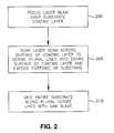
- FIG. 2is a flow chart of a first exemplary method of the present invention
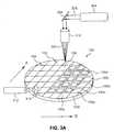
- FIGS. 3A and 3Bare diagrams of a first exemplary embodiment of the present invention.
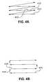
- FIG. 4Ais an illustration of saw blade motion
- FIG. 4Bis an illustration of the laser beam motion of the exemplary embodiment of the present invention.
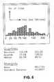
- FIG. 5is a statistical chart representing the backside chipping distribution of a silicon wafer with coatings where laser scribing assisted dicing, according to an exemplary embodiment of the present invention, was performed;
- FIG. 6is a statistical chart representing the backside chipping distribution of a silicon wafer with coatings where conventional single step dicing (untreated wafer) was performed;
- FIG. 7is a diagram of a second exemplary embodiment of the present invention.
- FIGS. 8A and 8Bare diagrams of a third exemplary embodiment of the present invention.
- FIG. 9is a diagram of a fourth exemplary embodiment of the present invention.
- FIG. 10is a flow chart of an exemplary method of the present invention.
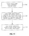
- FIG. 11is a flow chart of a second exemplary method of the present invention.
- FIG. 12is a flow chart of a third exemplary method of the present invention.
- FIG. 13is a flow chart of a fourth exemplary method of the present invention.
- the quality of the diceis directly related to the minimization of chipping (front and back) during the dicing operation.
- the inventorhas determined that by removing all the layers on top of the silicon substrate using a non-mechanical approach, in the area where the substrate will be cut through, throughput is dramatically increased (by about a factor of two), front side chipping (FSC) is significantly reduced (if not completely eliminated), BSC is minimized, and device yield is increased as well.
- FSCfront side chipping
- FIG. 2a flow chart of an exemplary embodiment of the present invention is shown.
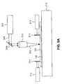
- FIGS. 3A and 3Ba first exemplary embodiment of the wafer singulating apparatus 300 is shown.
- laser beam 306 from laser 304(shown in FIGS. 3A and 3B) is directed by folding mirror 308 and focused by lens 310 , as focused beam 302 , onto coating layers 106 which overlie the surface of substrate 100 .
- focused laser beam 302might also be focused at a point above or below the surface of coating layers 106 or substrate 100 .
- focused laser beam 302is scanned across the surface of substrate coating layers 106 in a linear motion (in direction A for example) to remove all layers 106 by evaporation and form desired scribe lines 102 .
- the upper layers on top of the wafer surfaceare a combination of passivation layers, dielectrics, oxides, nitrides and metal pads. In most standard ICs, the total thickness of all these layers is usually less than 20 microns. The individual thickness of each layer is usually less than one micron, with the exception of the polymer layer having a thickness of few microns. The optical properties, such as absorption, reflection, and index of refraction of these layers are very different from one layer to another and from that of the silicon substrate.
- One of the major concerns when processing IC wafers with laser irradiationis the high sensitivity of the device to heating and thermal damage. Excessive heating of the substrate can reduce device performance, reliability and even cause instant device failure. It is therefore necessary to use an appropriate range of laser frequencies that are strongly absorbed in the upper layers, but with minimal absorption within the substrate.
- One of the most suitable lasers for the suggested process in this embodimentis the CO 2 laser irradiating in the far infrared region of the spectrum at a wavelength of about 10.6 microns, for example.
- the absorption coefficient of the CO 2 laser energy by siliconis practically zero, and is considerably lower (by about an order of magnitude, i.e.
- UVExcimer
- U.S. Pat. No. 5,151,389 to Zappella, and U.S. Pat. No. 5,552,345 to Schrantz et al.are examples of sources whose energy is readily absorbed by silicon.
- the use of lasers emitting energy in the UV frequency rangecan significantly damage the silicon wafer, while the present embodiment overcomes this major deficiency by using laser radiation that is not absorbed by the silicon substrate.
- the siliconcannot be heated directly by far infrared laser radiation, while the upper coatings over the silicon substrate are partially or completely removed by the CO 2 laser beam due to the much larger absorption coefficient of the layers relative to that of the silicon substrate.
- An analogous approachis used in the well known process of etching, where a stop etch layer is used to increase process robustness, accuracy, and to protect other layers.
- the silicon substrateacts as a stop etch layer for the laser irradiation.
- the focused laser beam 302is about 50 ⁇ m in diameter, although other diameters may be used as necessary.
- the focused laser beam diametershould preferably be larger than the thickness of the dicing blade ( 314 in FIGS. 3A and 3B), however, in order to completely eliminate any front side chipping of the wafer.
- 104 focused laser beam 302removes only the layers 106 on top of silicon substrate 100 , resulting in minimal indirect heating of the silicon substrate.
- the mechanical saw dicing(described in detail below) of the silicon substrate where dies are singulated.
- the laser assembly 322(which includes laser 304 , folding mirror 308 and lens 310 ) is stationary while the substrate 100 is moved in direction A, for example, using a conventional X-Y table 316 onto which the substrate 100 is mounted (by vacuum for example), to form streets 102 .
- substrate 100is translated in direction B by X-Y table 316 and the process is repeated for an additional street 102 .
- substrate 100is rotated by about 90° so that the process may be repeated to form streets 104 in substrate 100 .
- laser assembly 322may be moved relative to a stationary substrate 100 in either or both the X and Y directions.
- substrate 100is diced by penetrating substrate 100 along scribe lines 102 , 104 with saw blade 314 , under control of motor/spindle assembly 312 to form dies 100 a , 100 b , etc.
- saw blade 314is shown positioned lateral to focused laser beam 302 , the invention is not so limited, in that saw blade 314 may be placed essentially linear to focused laser beam 302 to provide for a more compact design.
- laser scribingmay be performed at a much higher feed rate than the conventional step cut dicing process to remove the top layers over the substrate. It should be noted, however, that the feed rates of the abrasive dicing, which follows the laser scribing, and the scribing are not necessarily the same. For example, scribing velocities can reach up to 600 mm/sec, which is about an order of magnitude greater than a conventional feed rate used in the dicing process.
- FIGS. 4A and 4BAnother advantage of the exemplary laser scribe process over conventional dicing is represented in FIGS. 4A and 4B. While dicing with a saw blade, the blade needs to penetrate the wafer from a particular direction (motion 400 , shown in FIG. 4A). Therefore, in order to make successive cuts, the blade motion has a zigzag form as shown in FIG. 4A (motion 400 followed by motion 402 , etc.) This approach is time consuming, however, since during the return time (motion 402 ) the blade can not cut. According to the exemplary embodiment of the present invention, since the laser scribing is a contact-less process the laser can operate in both directions (staggered mode) as is shown in FIG. 4B (motion 400 , followed by motion 404 , followed by motion 406 , etc.) Therefore, the only non-scribing time is during motion 406 from a dicing street to the next dicing street.
- a wafer(substrate) was treated with a CO 2 laser beam to remove all of the coatings from the streets of the wafer (without any direct effect on the silicon substrate) prior to cutting, in order to eliminate FSC and decrease BSC.
- the waferwas treated with a uniform level of energy to remove the coatings over the substrate by evaporation. All the streets 102 , 104 were treated according to the same parameters.
- the parameters of the exemplary CO 2 laserwere as follows:
- Feed rate16′′/sec (406.4 mm/sec)
- the waferwas diced with a saw blade using the following parameters:
- Feed rate2.165′′/sec (55 mm/sec),
- Blade type2′′ (50.8 mm) diameter, nickel binder, approximately 0.0012 in. (0.030 mm) thick.
- FIG. 5is the statistical analysis of the BSC result where the upper layers are evaporated from the street according to the first exemplary embodiment before dicing the substrate. As shown in FIG. 5, the maximum BSC is about 83 ⁇ m and the average BSC is about 31 ⁇ m.
- FIG. 6is a statistical layout of the BSC result where the upper coatings were not removed according to the exemplary process before dicing the substrate. As shown in FIG. 6, the maximum BSC is about 202 ⁇ m and the average BSC is about 99 ⁇ m.
- the BSC improvement achievedis more than three times than the results achieved using the conventional single blade, single cut dicing method.
- the laseris used primarily to remove various surface coatings, without damaging the edges of the scribe line.
- the improved BSCresults from the removal of all the coating layers that typically clog a dicing blade resulting in excessive backside chipping.
- the spindle speedmay be at least 2,000 RPM and may be as high as 60,000 RPM.
- other wavelengths of laser irradiationmay be used such that their absorption coefficient within the coating layers 106 is significantly higher (by about at least an order of magnitude based on the wavelength of the laser) than that of the substrate.
- Use of these different lasersmay produce varying degrees of BSC improvement. It is contemplated that lasers having wavelengths between about 1.2 and 15 microns may be used, preferably between about 9 and 11 microns, and most preferably about 9.3, 9.6 or 10.6 microns.
- lasers with specific power ratingsare illustrated above, it is contemplated that lower or higher powered lasers may be used as desired. For example, it is contemplated that lasers having power rating as low as 5 Watts may be used to achieve reduced BSC.
- FIG. 7Aa second exemplary embodiment of the present invention is shown and described in the flow chart of FIG. 10.
- the second exemplary embodimentis similar to the first exemplary embodiment except for the addition of second laser assembly 700 , including laser 704 (emitting laser beam 706 ) and mirror 708 to direct laser beam 706 onto focusing lens 710 .
- the output of focusing lens 710is focused beam 702 similar to focused beam 302 .
- the advantage of the second exemplary embodimentis that substrate 100 may be scribed about twice as fast as in the first exemplary embodiment.
- FIG. 7BAnother approach to the second exemplary embodiment is shown in FIG. 7B.
- a single laser source 720 having about twice the power of laser source 304is used to generate laser beam 722 , which is then split into two essentially identical laser beams 724 and 726 with beam splitter 712 .
- the laser beams 724 and 726are then used to generate focused laser beams 302 and 702 , respectively, according to the process described above.
- laser beams 306 , 706 from laser 304 , 704are directed by mirrors 308 , 708 and focused by lens 310 , 710 , as focused beam 302 , 702 , onto coating layers 106 of substrate 100 .
- focused laser beams 302 , 702may also be focused at a point above or below the surface of coating layers 106 or substrate 100 .
- Step 1005focused laser beams 302 , 702 are scanned across the surface of the substrate coating layers 106 in a linear motion to remove portions all layers 106 by evaporation and form scribe lines 102 , 104 .
- substrate 100is diced by penetrating substrate 100 along scribe lines 102 , 104 with saw blade 314 , under control of motor/spindle assembly 312 , to form dies 100 a , 100 b , etc.
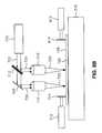
- FIGS. 8A and 8Ba third exemplary embodiment of the present invention is shown and described in the flow chart of FIG. 11.
- the third exemplary embodimentis similar to the first exemplary embodiment (Steps 1100 and 1105 ) except for the addition of a second motor/spindle assembly 812 and dicing blade 814 .
- saw blades 314 , 814penetrate substrate 100 (along streets 104 , 106 ) either i) after the entire substrate is scribed along either one or both directions or ii) while the focused laser beam 302 is scribing other portions of substrate 100 .
- substrate 100is attached to table 316 with detachable means, such as NITTO tape 820 .
- substrate 100may also be detachably mounted to table 316 using vacuum.
- the fourth exemplary embodimentis essentially a combination of the second and third exemplary embodiments. As such, a description of the constituent parts and their respective function(s) is not repeated.
- the fourth exemplary embodimenthas the added advantage of not only increased throughput with respect to scribing the coating layers, but also increased throughput with respect to penetrating the substrate with the saw blade to form the various dies.
- saw blade(s) 314 and/or 814may be used to saw along that scribe line(s). Subsequent scribe lines may then be formed and sawed in sequence in the first direction across the surface of the substrate followed by a similar procedure along the second direction of the substrate to form the dice.
- the laser scribing and dicingmay be performed in alternate ways. Flowcharts of these alternatives are illustrated in FIGS. 12 and 13.
- focused beam 302is directed onto coating layers 106 of substrate 100 .
- focused laser beam 302is scanned across the surface of the substrate coating layers 106 in a linear motion (and in a first direction) to remove portions all layers 106 by evaporation and form scribe lines 102 .
- substrate 100is rotated (preferably at an angle of about 90°) and focused laser beam 302 is scanned across the surface of the substrate coating layers 106 in a second direction to remove portions all layers 106 by evaporation and form scribe lines 104 .
- substrate 100is diced by penetrating substrate 100 along scribe lines 104 with saw blade 314 , under control of motor/spindle assembly 312 .
- substrate 100is rotated to its original position and diced by penetrating substrate 100 along scribe lines 102 with saw blade 314 , under control of motor/spindle assembly 312 , to form dies 100 a , 100 b , etc.
- This exemplary methodmay be performed on either a single machine incorporating both the laser scribing apparatus and the dicing apparatus, or with two machines, a first machine incorporating the laser scriber and the second machine incorporating the dicing mechanism.
- the scribed wafermay be automatically transported between the laser scriber and the dicer by means of a conveyer system, or other suitable means.
- Step 1300focused beam 302 is directed onto coating layers 106 of substrate 100 .
- Step 1305focused laser beam 302 is scanned across the surface of the substrate coating layers 106 in a linear motion (and in a first direction) to remove portions all layers 106 by evaporation and form scribe lines 102 .
- substrate 100is diced by penetrating substrate 100 along scribe lines 102 with saw blade 314 , under control of motor/spindle assembly 312 .
- substrate 100is rotated (preferably at an angle of about 90°) and focused laser beam 302 is scanned across the surface of the substrate coating layers 106 in a second direction to remove portions all layers 106 by evaporation and form scribe lines 104 .
- substrate 100is diced by penetrating substrate 100 along scribe lines 104 with saw blade 314 , under control of motor/spindle assembly 312 , to form dies 100 a , 100 b , etc.
Landscapes
- Engineering & Computer Science (AREA)
- Mechanical Engineering (AREA)
- Physics & Mathematics (AREA)
- Optics & Photonics (AREA)
- Plasma & Fusion (AREA)
- General Physics & Mathematics (AREA)
- Condensed Matter Physics & Semiconductors (AREA)
- Manufacturing & Machinery (AREA)
- Computer Hardware Design (AREA)
- Microelectronics & Electronic Packaging (AREA)
- Power Engineering (AREA)
- Mining & Mineral Resources (AREA)
- Dicing (AREA)
- Laser Beam Processing (AREA)
Abstract
Description
- This application is a Continuation-in-Part of pending application Ser. No. 09/817,959 filed on Mar. 27, 2001, which is a Continuation-in-Part of pending application Ser. No. 09/327,722 filed on Jun. 8, 1999.[0001]
- This invention relates generally to dicing of semiconductor wafers. More specifically, the present invention relates to a method and apparatus for laser scribing followed by mechanical dicing of the semiconductor wafers.[0002]
- Die separation, or dicing, by sawing is the process of cutting a microelectronic substrate into its individual circuit die with a rotating circular abrasive saw blade. This process has proven to be the most efficient and economical method in use today. It provides versatility in selection of depth and width (kerf) of cut, as well as selection of surface finish, and can be used to saw either partially or completely through a wafer or substrate.[0003]
- Wafer dicing technology has progressed rapidly, and dicing is now a mandatory procedure in most front-end semiconductor packaging operations. It is used extensively for separation of die on silicon integrated circuit wafers.[0004]
- Increasing use of microelectronic technology in microwave and hybrid circuits, memories, computers, defense and medical electronics has created an array of new and difficult problems for the industry. More expensive and exotic materials, such as sapphire, garnet, alumina, ceramic, glass, quartz, ferrite, and other hard, brittle substrates, are being used. They are often combined to produce multiple layers of dissimilar materials, thus adding further to the dicing problems. The high cost of these substrates, together with the value of the circuits fabricated on them, makes it difficult to accept anything less than high yield at the die-separation phase.[0005]
- Dicing is the mechanical process of machining with abrasive particles. It is assumed that this process mechanism is similar to creep grinding. As such, a similarity may be found in material removal behavior between dicing and grinding. The size of the dicing blades used for die separation, however, makes the process unique. Typically, the blade thickness ranges from 0.6 mils to 50 mils (0.015 mm to 1.27 mm), and diamond particles (the hardest known material) are used as the abrasive material ingredient. Dicing saw blades are made in the form of an annular disc that is either clamped between the flanges of a hub or built on a hub that accurately positions the thin flexible saw blade. Because of the diamond dicing blade's extreme fineness, compliance with a strict set of parameters is imperative, and even the slightest deviation from the norm can result in complete failure.[0006]
- FIG. 1 is an isometric view of a[0007]
semiconductor wafer 100 during the fabrication of semiconductor devices. Aconventional semiconductor wafer 100 may have a plurality of chips, or dies,100a,100b, . . . formed on its top surface. In order to separate thechips wafer 100, a series of orthogonal lines or “streets”102,104 are cut into thewafer 100. This process is also known as dicing the wafer. - IC wafers are coated with various layers such as passivation of oxides or nitrides, dielectrics, polymer coatings, and aluminum as well as copper metal pads (all collectively shown as[0008]106 in FIG. 1). The wafer scribe lines (streets) reflect similar coatings on the chips, since all of the test devices and alignment marks are located within the scribe line borders. The wafer streets are therefore fully or partially coated with different materials and are largely non-homogeneous. This combination of materials has a significant effect on wafer dicing and die edge quality. When conventional dicing technology is used, such as a single blade and a single cut, the die edge on the bottom side of semiconductor wafer suffers severe backside chipping (BSC). In addition, on the topside of the wafer, problems at the die edge include cracking of the passivation and dielectric layers, the smearing or tearing of the metal pads, and the formation of polymer slivers.
- One approach to overcome the aforementioned die edge problems is a mechanical dual dicing method. This method is a combination of two cuts (step cut), the first one being shallow and the second one being a through cut. The purpose of the first cut is to remove all the[0009]
coatings 106 from thestreets metal pads 106 from thestreets - There are many disadvantages, however, to the step cut. First, the process throughput is reduced dramatically, since instead of one pass in the street, two passes are required. Second, the mechanical removal of the coatings creates residual cracks, which, in turn, cause further deterioration of the dice. Third, when the bevel blade wears out, the kerf gets wider and this requires frequent handling and replacement of the blade. Forth, the price of bevel blades is more expensive by a factor of five compared to a standard blade. All these drawbacks result in a high cost is of ownership with regard to the step cut process.[0010]
- There are other disadvantages regarding the beveled cut. Namely, blade penetration height must be carefully monitored, because for each one micron of penetration, the kerf widens by about two microns. In addition, the beveled blade may insert hidden damage into the die edge, in the form of cracks for example. Visual inspection of dice after dicing (an industry standard) is not capable of detecting this damage.[0011]
- In view of the shortcomings of the prior art, there is a need to develop a method to cut die having various coating layers and test structures in the wafer scribe lane so as to increase throughput, minimize the backside chipping, and to increase the yield of useable circuits.[0012]
- In view of the shortcomings of the prior art, it is an object of the present invention to optimize the dicing process and minimize bottom side chipping (BSC) of semiconductor wafers.[0013]
- The present invention is a method for dicing a semiconductor substrate by focusing a laser beam onto a coating layer over a top surface of the substrate; absorbing energy into only the layer; forming scribe lines on the substrate surface by scanning the laser beam across the surface of the substrate to evaporate only portions of the layer; and dicing the substrate along the scribe lines with a saw blade.[0014]
- According to another aspect of the invention, the laser emits infrared radiation.[0015]
- According to still another aspect of the invention, the scribe line removes all the layers over the silicon wafer, with minimal heat damage to the silicon substrate.[0016]
- These and other aspects of the invention are set forth below with reference to the drawings and the description of exemplary embodiments of the invention.[0017]
- The invention is best understood from the following detailed description when read in connection with the accompanying drawing. It is emphasized that, according to common practice, the various features of the drawing are not to scale. On the contrary, the dimensions of the various features are arbitrarily expanded or reduced for clarity. Included in the drawing are the following Figures:[0018]
- FIG. 1 is an isometric view of a semiconductor wafer used to form semiconductor devices;[0019]
- FIG. 2 is a flow chart of a first exemplary method of the present invention;[0020]
- FIGS. 3A and 3B are diagrams of a first exemplary embodiment of the present invention;[0021]
- FIG. 4A is an illustration of saw blade motion;[0022]
- FIG. 4B is an illustration of the laser beam motion of the exemplary embodiment of the present invention;[0023]
- FIG. 5 is a statistical chart representing the backside chipping distribution of a silicon wafer with coatings where laser scribing assisted dicing, according to an exemplary embodiment of the present invention, was performed;[0024]
- FIG. 6 is a statistical chart representing the backside chipping distribution of a silicon wafer with coatings where conventional single step dicing (untreated wafer) was performed;[0025]
- FIG. 7 is a diagram of a second exemplary embodiment of the present invention;[0026]
- FIGS. 8A and 8B are diagrams of a third exemplary embodiment of the present invention;[0027]
- FIG. 9 is a diagram of a fourth exemplary embodiment of the present invention;[0028]
- FIG. 10 is a flow chart of an exemplary method of the present invention;[0029]
- FIG. 11 is a flow chart of a second exemplary method of the present invention;[0030]
- FIG. 12 is a flow chart of a third exemplary method of the present invention; and[0031]
- FIG. 13 is a flow chart of a fourth exemplary method of the present invention.[0032]
- In the manufacture of semiconductor devices, individual chips are cut from a large wafer using a very high speed rotating saw blade. In essence, the saw blade grinds away a portion of the wafer along linear streets or kerfs ([0033]102,104 as shown in FIG. 1) in one direction followed by a similar second operation in an orthogonal direction.
- The quality of the dice (chips) is directly related to the minimization of chipping (front and back) during the dicing operation. The inventor has determined that by removing all the layers on top of the silicon substrate using a non-mechanical approach, in the area where the substrate will be cut through, throughput is dramatically increased (by about a factor of two), front side chipping (FSC) is significantly reduced (if not completely eliminated), BSC is minimized, and device yield is increased as well.[0034]
- Referring to FIG. 2, a flow chart of an exemplary embodiment of the present invention is shown. Referring to FIGS. 3A and 3B, a first exemplary embodiment of the wafer singulating apparatus[0035]300 is shown.
- In FIG. 2, at[0036]
Step 200,laser beam 306 from laser304 (shown in FIGS. 3A and 3B) is directed by foldingmirror 308 and focused bylens 310, asfocused beam 302, onto coating layers106 which overlie the surface ofsubstrate 100. It should be noted thatfocused laser beam 302 might also be focused at a point above or below the surface ofcoating layers 106 orsubstrate 100. AtStep 205,focused laser beam 302 is scanned across the surface of substrate coating layers106 in a linear motion (in direction A for example) to remove alllayers 106 by evaporation and form desired scribe lines102. - The upper layers on top of the wafer surface are a combination of passivation layers, dielectrics, oxides, nitrides and metal pads. In most standard ICs, the total thickness of all these layers is usually less than 20 microns. The individual thickness of each layer is usually less than one micron, with the exception of the polymer layer having a thickness of few microns. The optical properties, such as absorption, reflection, and index of refraction of these layers are very different from one layer to another and from that of the silicon substrate.[0037]
- One of the major concerns when processing IC wafers with laser irradiation is the high sensitivity of the device to heating and thermal damage. Excessive heating of the substrate can reduce device performance, reliability and even cause instant device failure. It is therefore necessary to use an appropriate range of laser frequencies that are strongly absorbed in the upper layers, but with minimal absorption within the substrate. One of the most suitable lasers for the suggested process in this embodiment is the CO[0038]2laser irradiating in the far infrared region of the spectrum at a wavelength of about 10.6 microns, for example. The absorption coefficient of the CO2laser energy by silicon is practically zero, and is considerably lower (by about an order of magnitude, i.e. a factor of 10, and preferably at least an order of magnitude) than the absorption coefficient of the coating layers. On the contrary, silicon heavily absorbs (absorption coefficient of 106cm−1) energy in the UV range of the spectrum, such as a wavelength of about 200 nm. Laser energy sources, such as Excimer (UV) laser sources, described in the prior art to process silicon (U.S. Pat. No. 5,151,389 to Zappella, and U.S. Pat. No. 5,552,345 to Schrantz et al.) are examples of sources whose energy is readily absorbed by silicon. Nevertheless, the use of lasers emitting energy in the UV frequency range can significantly damage the silicon wafer, while the present embodiment overcomes this major deficiency by using laser radiation that is not absorbed by the silicon substrate. The silicon cannot be heated directly by far infrared laser radiation, while the upper coatings over the silicon substrate are partially or completely removed by the CO2laser beam due to the much larger absorption coefficient of the layers relative to that of the silicon substrate. An analogous approach is used in the well known process of etching, where a stop etch layer is used to increase process robustness, accuracy, and to protect other layers. In the aforementioned embodiment, the silicon substrate acts as a stop etch layer for the laser irradiation. In U.S. Pat. No. 4,716,270 to Gnanamuthu et al. totally different physics are used to differentiate between laser processing of two layers of material. In Gnanamuthu et al. the workpiece is a metal coated with an organic polymer, and the differentiation between the laser processing on the two layers is based on a reflection principle, in which the laser radiation is highly reflected from the underlying metal substrate. By contrast, the exemplary embodiment of the present invention is capable of removing thin metal layers on top of the wafer substrate, despite their high reflectivity to the laser radiation. This is possible because the exemplary process is based on absorption of the laser energy rather than reflection.
- In an exemplary embodiment of the present invention, the[0039]
focused laser beam 302 is about 50 μm in diameter, although other diameters may be used as necessary. The focused laser beam diameter should preferably be larger than the thickness of the dicing blade (314 in FIGS. 3A and 3B), however, in order to completely eliminate any front side chipping of the wafer. In formingstreets focused laser beam 302 removes only thelayers 106 on top ofsilicon substrate 100, resulting in minimal indirect heating of the silicon substrate. Complementary to the laser scribing process is the mechanical saw dicing (described in detail below) of the silicon substrate where dies are singulated. - In an exemplary embodiment, the laser assembly[0040]322 (which includes
laser 304,folding mirror 308 and lens310) is stationary while thesubstrate 100 is moved in direction A, for example, using a conventional X-Y table316 onto which thesubstrate 100 is mounted (by vacuum for example), to formstreets 102. As eachstreet 102 is completed,substrate 100 is translated in direction B by X-Y table316 and the process is repeated for anadditional street 102. - After all of the[0041]
streets 102 are formed,substrate 100 is rotated by about 90° so that the process may be repeated to formstreets 104 insubstrate 100. Alternatively, laser assembly322 may be moved relative to astationary substrate 100 in either or both the X and Y directions. - Referring again to FIG. 2, at[0042]
Step 210,substrate 100 is diced by penetratingsubstrate 100 alongscribe lines saw blade 314, under control of motor/spindle assembly 312 to form dies100a,100b, etc. - Although for simplicity of illustration saw[0043]
blade 314 is shown positioned lateral tofocused laser beam 302, the invention is not so limited, in thatsaw blade 314 may be placed essentially linear tofocused laser beam 302 to provide for a more compact design. - One major advantage of laser scribing is that laser scribing may be performed at a much higher feed rate than the conventional step cut dicing process to remove the top layers over the substrate. It should be noted, however, that the feed rates of the abrasive dicing, which follows the laser scribing, and the scribing are not necessarily the same. For example, scribing velocities can reach up to 600 mm/sec, which is about an order of magnitude greater than a conventional feed rate used in the dicing process.[0044]
- Another advantage of the exemplary laser scribe process over conventional dicing is represented in FIGS. 4A and 4B. While dicing with a saw blade, the blade needs to penetrate the wafer from a particular direction ([0045]
motion 400, shown in FIG. 4A). Therefore, in order to make successive cuts, the blade motion has a zigzag form as shown in FIG. 4A (motion 400 followed bymotion 402, etc.) This approach is time consuming, however, since during the return time (motion402) the blade can not cut. According to the exemplary embodiment of the present invention, since the laser scribing is a contact-less process the laser can operate in both directions (staggered mode) as is shown in FIG. 4B (motion 400, followed bymotion 404, followed bymotion 406, etc.) Therefore, the only non-scribing time is duringmotion 406 from a dicing street to the next dicing street. - Yet another advantage of the laser scribing over the step-bevel cut is eliminating the need for expensive blades, and allowing the possibility of sealing the passivation layer using the laser beam, thereby avoiding crack formation.[0046]
- In a first exemplary method a wafer (substrate) was treated with a CO[0047]2laser beam to remove all of the coatings from the streets of the wafer (without any direct effect on the silicon substrate) prior to cutting, in order to eliminate FSC and decrease BSC. The wafer was treated with a uniform level of energy to remove the coatings over the substrate by evaporation. All the
streets - Power=20 Watts[0048]
- Feed rate=16″/sec (406.4 mm/sec)[0049]
- Following laser scribing, the wafer was diced with a saw blade using the following parameters:[0050]
- Feed rate: 2.165″/sec (55 mm/sec),[0051]
- Spindle speed: 40,000 rpm,[0052]
- Blade type: 2″ (50.8 mm) diameter, nickel binder, approximately 0.0012 in. (0.030 mm) thick.[0053]
- The wafer was subjected to microscopic and statistical analysis to determine the amount of BSC resulting from the dicing operation. FIG. 5 is the statistical analysis of the BSC result where the upper layers are evaporated from the street according to the first exemplary embodiment before dicing the substrate. As shown in FIG. 5, the maximum BSC is about 83 μm and the average BSC is about 31 μm.[0054]
- By contrast, FIG. 6 is a statistical layout of the BSC result where the upper coatings were not removed according to the exemplary process before dicing the substrate. As shown in FIG. 6, the maximum BSC is about 202 μm and the average BSC is about 99 μm.[0055]
- Overall, using the exemplary embodiment, the BSC improvement achieved is more than three times than the results achieved using the conventional single blade, single cut dicing method.[0056]
- The laser is used primarily to remove various surface coatings, without damaging the edges of the scribe line. The improved BSC results from the removal of all the coating layers that typically clog a dicing blade resulting in excessive backside chipping.[0057]
- Although specific a spindle speed is illustrated, it is contemplated that the spindle speed may be at least 2,000 RPM and may be as high as 60,000 RPM. Furthermore, instead of a CO[0058]2laser, other wavelengths of laser irradiation may be used such that their absorption coefficient within the coating layers106 is significantly higher (by about at least an order of magnitude based on the wavelength of the laser) than that of the substrate. Use of these different lasers may produce varying degrees of BSC improvement. It is contemplated that lasers having wavelengths between about 1.2 and 15 microns may be used, preferably between about 9 and 11 microns, and most preferably about 9.3, 9.6 or 10.6 microns.
- Although lasers with specific power ratings are illustrated above, it is contemplated that lower or higher powered lasers may be used as desired. For example, it is contemplated that lasers having power rating as low as 5 Watts may be used to achieve reduced BSC.[0059]
- Referring now to FIG. 7A, a second exemplary embodiment of the present invention is shown and described in the flow chart of FIG. 10. The second exemplary embodiment is similar to the first exemplary embodiment except for the addition of[0060]
second laser assembly 700, including laser704 (emitting laser beam706) andmirror 708 todirect laser beam 706 onto focusinglens 710. The output of focusinglens 710 is focusedbeam 702 similar tofocused beam 302. The advantage of the second exemplary embodiment is thatsubstrate 100 may be scribed about twice as fast as in the first exemplary embodiment. - Another approach to the second exemplary embodiment is shown in FIG. 7B. As shown in FIG. 7B, a[0061]
single laser source 720 having about twice the power oflaser source 304 is used to generatelaser beam 722, which is then split into two essentiallyidentical laser beams beam splitter 712. Thelaser beams focused laser beams - Referring to FIG. 10, a flow chart of the second exemplary embodiment is shown. At[0062]
Step 1000,laser beams laser mirrors lens focused beam substrate 100. As in the first exemplary embodiment,focused laser beams coating layers 106 orsubstrate 100. AtStep 1005, focusedlaser beams layers 106 by evaporation andform scribe lines Step 1010,substrate 100 is diced by penetratingsubstrate 100 alongscribe lines saw blade 314, under control of motor/spindle assembly 312, to form dies100a,100b, etc. - Referring now to FIGS. 8A and 8B, a third exemplary embodiment of the present invention is shown and described in the flow chart of FIG. 11. The third exemplary embodiment is similar to the first exemplary embodiment ([0063]
Steps 1100 and1105) except for the addition of a second motor/spindle assembly 812 anddicing blade 814. In this exemplary embodiment, atStep 1110, sawblades streets 104,106) either i) after the entire substrate is scribed along either one or both directions or ii) while thefocused laser beam 302 is scribing other portions ofsubstrate 100. As shown in FIG. 8B,substrate 100 is attached to table316 with detachable means, such asNITTO tape 820. As described above,substrate 100 may also be detachably mounted to table316 using vacuum. - Referring now to FIGS. 9A and 9B, a fourth exemplary embodiment of the present invention is shown. The fourth exemplary embodiment is essentially a combination of the second and third exemplary embodiments. As such, a description of the constituent parts and their respective function(s) is not repeated. The fourth exemplary embodiment has the added advantage of not only increased throughput with respect to scribing the coating layers, but also increased throughput with respect to penetrating the substrate with the saw blade to form the various dies.[0064]
- Furthermore, rather that scribing the entire surface of the substrate before sawing, it is contemplated that, as each scribe line is formed, saw blade(s)[0065]314 and/or814 (depending on the layout of the apparatus) may be used to saw along that scribe line(s). Subsequent scribe lines may then be formed and sawed in sequence in the first direction across the surface of the substrate followed by a similar procedure along the second direction of the substrate to form the dice.
- It is also contemplated that the laser scribing and dicing may be performed in alternate ways. Flowcharts of these alternatives are illustrated in FIGS. 12 and 13. In FIG. 12, at[0066]
Step 1200, focusedbeam 302, is directed onto coating layers106 ofsubstrate 100. AtStep 1205, focusedlaser beam 302 is scanned across the surface of the substrate coating layers106 in a linear motion (and in a first direction) to remove portions alllayers 106 by evaporation and form scribe lines102. AtStep 1210,substrate 100 is rotated (preferably at an angle of about 90°) andfocused laser beam 302 is scanned across the surface of the substrate coating layers106 in a second direction to remove portions alllayers 106 by evaporation and form scribe lines104. AtStep 1215,substrate 100 is diced by penetratingsubstrate 100 alongscribe lines 104 withsaw blade 314, under control of motor/spindle assembly 312. AtStep 1220,substrate 100 is rotated to its original position and diced by penetratingsubstrate 100 alongscribe lines 102 withsaw blade 314, under control of motor/spindle assembly 312, to form dies100a,100b, etc. This exemplary method may be performed on either a single machine incorporating both the laser scribing apparatus and the dicing apparatus, or with two machines, a first machine incorporating the laser scriber and the second machine incorporating the dicing mechanism. In the latter, the scribed wafer may be automatically transported between the laser scriber and the dicer by means of a conveyer system, or other suitable means. - Referring now to FIG. 13, a fourth exemplary method is illustrated. At[0067]
Step 1300, focusedbeam 302, is directed onto coating layers106 ofsubstrate 100. AtStep 1305, focusedlaser beam 302 is scanned across the surface of the substrate coating layers106 in a linear motion (and in a first direction) to remove portions alllayers 106 by evaporation and form scribe lines102. AtStep 1310,substrate 100 is diced by penetratingsubstrate 100 alongscribe lines 102 withsaw blade 314, under control of motor/spindle assembly 312. AtStep 1315,substrate 100 is rotated (preferably at an angle of about 90°) andfocused laser beam 302 is scanned across the surface of the substrate coating layers106 in a second direction to remove portions alllayers 106 by evaporation and form scribe lines104. AtStep 1320,substrate 100 is diced by penetratingsubstrate 100 alongscribe lines 104 withsaw blade 314, under control of motor/spindle assembly 312, to form dies100a,100b, etc. - Although the above two examples discuss scribing with a single laser beam, it is contemplated that these methods may also be performed using the dual beams described above.[0068]
- Although the invention has been described with reference to exemplary embodiments, it is not limited thereto. Rather, the appended claims should be construed to include other variants and embodiments of the invention, which may be made by those skilled in the art without departing from the true spirit and scope of the present invention.[0069]
Claims (44)
Priority Applications (5)
| Application Number | Priority Date | Filing Date | Title |
|---|---|---|---|
| US09/845,890US6420245B1 (en) | 1999-06-08 | 2001-04-30 | Method for singulating semiconductor wafers |
| JP2001319928AJP2002329686A (en) | 2001-04-30 | 2001-10-17 | Apparatus and method for dividing a semiconductor wafer into individual pieces |
| TW090126281ATW512451B (en) | 2001-04-30 | 2001-10-24 | Apparatus and method for singulating semiconductor wafers |
| EP02003300AEP1255280A3 (en) | 2001-04-30 | 2002-02-25 | Apparatus and method for dicing semiconductor wafers |
| JP2007299916AJP2008066751A (en) | 2001-04-30 | 2007-11-19 | Apparatus and method for dividing a semiconductor wafer into individual pieces |
Applications Claiming Priority (3)
| Application Number | Priority Date | Filing Date | Title |
|---|---|---|---|
| US32772299A | 1999-06-08 | 1999-06-08 | |
| US09/817,959US6555447B2 (en) | 1999-06-08 | 2001-03-27 | Method for laser scribing of wafers |
| US09/845,890US6420245B1 (en) | 1999-06-08 | 2001-04-30 | Method for singulating semiconductor wafers |
Related Parent Applications (1)
| Application Number | Title | Priority Date | Filing Date |
|---|---|---|---|
| US09/817,959Continuation-In-PartUS6555447B2 (en) | 1999-06-08 | 2001-03-27 | Method for laser scribing of wafers |
Publications (2)
| Publication Number | Publication Date |
|---|---|
| US20020031899A1true US20020031899A1 (en) | 2002-03-14 |
| US6420245B1 US6420245B1 (en) | 2002-07-16 |
Family
ID=25296336
Family Applications (1)
| Application Number | Title | Priority Date | Filing Date |
|---|---|---|---|
| US09/845,890Expired - Fee RelatedUS6420245B1 (en) | 1999-06-08 | 2001-04-30 | Method for singulating semiconductor wafers |
Country Status (4)
| Country | Link |
|---|---|
| US (1) | US6420245B1 (en) |
| EP (1) | EP1255280A3 (en) |
| JP (2) | JP2002329686A (en) |
| TW (1) | TW512451B (en) |
Cited By (43)
| Publication number | Priority date | Publication date | Assignee | Title |
|---|---|---|---|---|
| US6580054B1 (en) | 2002-06-10 | 2003-06-17 | New Wave Research | Scribing sapphire substrates with a solid state UV laser |
| US20040126996A1 (en)* | 2002-12-27 | 2004-07-01 | Kazuo Kobayashi | Method and apparatus for machining substrate |
| US20040188400A1 (en)* | 2001-09-10 | 2004-09-30 | Micron Technology, Inc. | Wafer dicing device and method |
| US6806544B2 (en) | 2002-11-05 | 2004-10-19 | New Wave Research | Method and apparatus for cutting devices from conductive substrates secured during cutting by vacuum pressure |
| US20040211750A1 (en)* | 2003-02-10 | 2004-10-28 | Palla Byron Joseph | Laser scribe on front side of semiconductor wafer |
| US20040221451A1 (en)* | 2003-05-06 | 2004-11-11 | Micron Technology, Inc. | Method for packaging circuits and packaged circuits |
| US6869861B1 (en) | 2001-03-08 | 2005-03-22 | Amkor Technology, Inc. | Back-side wafer singulation method |
| US20050070095A1 (en)* | 2003-09-30 | 2005-03-31 | Sujit Sharan | Protective layer during scribing |
| US20050095819A1 (en)* | 2002-06-10 | 2005-05-05 | New Wave Research | Method and apparatus for cutting devices from substrates |
| US20050139962A1 (en)* | 2003-12-30 | 2005-06-30 | Dani Ashay A. | Silicon wafer with soluable protective coating |
| US6943429B1 (en)* | 2001-03-08 | 2005-09-13 | Amkor Technology, Inc. | Wafer having alignment marks extending from a first to a second surface of the wafer |
| US20050202650A1 (en)* | 2004-03-08 | 2005-09-15 | Yoshihisa Imori | Method of dividing a wafer which has a low-k film formed on dicing lines |
| US6945844B2 (en)* | 2002-07-26 | 2005-09-20 | Cree, Inc. | Methods for dynamically controlling a semiconductor dicing saw |
| US20060172509A1 (en)* | 2003-07-02 | 2006-08-03 | Mahle Richard L | Method for reducing stress concentrations on a semiconductor wafer by surface laser treatment |
| US20060264064A1 (en)* | 2004-08-02 | 2006-11-23 | Micron Technology, Inc. | Zirconium-doped tantalum oxide films |
| US20060289966A1 (en)* | 2005-06-22 | 2006-12-28 | Dani Ashay A | Silicon wafer with non-soluble protective coating |
| US20070090099A1 (en)* | 2003-06-06 | 2007-04-26 | David Gillen | Laser machining using a surfactant film |
| US20070119831A1 (en)* | 2005-11-28 | 2007-05-31 | Electro Scientific Industries, Inc. | X & Y orthogonal cut direction processing with set beam separation using 45 degree beam split orientation apparatus and method |
| US20080054423A1 (en)* | 2001-10-08 | 2008-03-06 | Micron Technology, Inc. | Apparatus and method for packaging circuits |
| US7388172B2 (en) | 2003-02-19 | 2008-06-17 | J.P. Sercel Associates, Inc. | System and method for cutting using a variable astigmatic focal beam spot |
| US20080194080A1 (en)* | 2007-02-13 | 2008-08-14 | Huga Optotech Inc. | Method and product for dicing an optoelectronic semiconductor wafer |
| US20090017600A1 (en)* | 2007-07-13 | 2009-01-15 | Disco Corporation | Wafer dividing method using laser beam with an annular spot |
| US20110018143A1 (en)* | 2002-06-14 | 2011-01-27 | Swee Kwang Chua | Wafer level packaging |
| US20110124147A1 (en)* | 2009-05-20 | 2011-05-26 | Rofin-Baasel Lasertech Gmbh & Co. Kg | Method for separating silicon solar cells |
| WO2011100051A1 (en)* | 2010-02-12 | 2011-08-18 | Narayanan Srinivasamohan | Silicon wafers prepared from a beam having a plurality of wafers |
| WO2011126649A3 (en)* | 2010-03-31 | 2011-12-29 | Electro Scientific Industries, Inc. | Use of laser energy transparent stop layer to achieve minimal debris generation in laser scribing a multilayer patterned workpiece |
| US20120132629A1 (en)* | 2010-11-30 | 2012-05-31 | Electro Scientific Industries, Inc. | Method and apparatus for reducing taper of laser scribes |
| US20130256286A1 (en)* | 2009-12-07 | 2013-10-03 | Ipg Microsystems Llc | Laser processing using an astigmatic elongated beam spot and using ultrashort pulses and/or longer wavelengths |
| US8809166B2 (en)* | 2012-12-20 | 2014-08-19 | Nxp B.V. | High die strength semiconductor wafer processing method and system |
| EP2517227A4 (en)* | 2009-12-23 | 2015-04-22 | Intel Corp | Offset field grid for efficient wafer layout |
| US20150118797A1 (en)* | 2013-10-30 | 2015-04-30 | Taiwan Semiconductor Manufacturing Company, Ltd. | Method for Singulating Packaged Integrated Circuits and Resulting Structures |
| US9093518B1 (en)* | 2014-06-30 | 2015-07-28 | Applied Materials, Inc. | Singulation of wafers having wafer-level underfill |
| US20150255288A1 (en)* | 2014-03-06 | 2015-09-10 | Disco Corporation | Plate-like object processing method |
| US9165832B1 (en) | 2014-06-30 | 2015-10-20 | Applied Materials, Inc. | Method of die singulation using laser ablation and induction of internal defects with a laser |
| KR20160073920A (en)* | 2014-12-17 | 2016-06-27 | 가부시기가이샤 디스코 | Processing method of package substrate |
| DE102006000719B4 (en)* | 2005-01-05 | 2016-10-13 | Disco Corp. | Wafer dividing method |
| US20170151632A1 (en)* | 2015-05-12 | 2017-06-01 | Han's Laser Technology Industry Group Co., Ltd. | Laser processing method, apparatus for sapphire and storage medium |
| US20200039003A1 (en)* | 2015-06-12 | 2020-02-06 | Schuler Automation Gmbh & Co. Kg | Method and device for producing a sheet metal blank |
| US20200324374A1 (en)* | 2019-04-12 | 2020-10-15 | Skyworks Solutions, Inc. | Method of optimizing laser cutting of wafers for producing integrated circuit dies |
| US20220040800A1 (en)* | 2018-12-21 | 2022-02-10 | Tokyo Electron Limited | Substrate processing apparatus and substrate processing method |
| DE102020215016A1 (en) | 2020-11-30 | 2022-06-02 | Robert Bosch Gesellschaft mit beschränkter Haftung | Process for manufacturing a semiconductor device and semiconductor device |
| US20220359316A1 (en)* | 2019-10-30 | 2022-11-10 | Taiwan Semiconductor Manufacturing Company, Ltd. | Method of fabricating semiconductor structure |
| US12109651B2 (en) | 2018-04-03 | 2024-10-08 | Ilika Technologies Limited | Laser processing method for thin film structures |
Families Citing this family (70)
| Publication number | Priority date | Publication date | Assignee | Title |
|---|---|---|---|---|
| US20040112360A1 (en)* | 1998-02-12 | 2004-06-17 | Boucher John N. | Substrate dicing method |
| US6255621B1 (en) | 2000-01-31 | 2001-07-03 | International Business Machines Corporation | Laser cutting method for forming magnetic recording head sliders |
| AU7684001A (en)* | 2000-07-06 | 2002-01-21 | Bp Corp North America Inc | Partially transparent photovoltaic modules |
| JP4659300B2 (en) | 2000-09-13 | 2011-03-30 | 浜松ホトニクス株式会社 | Laser processing method and semiconductor chip manufacturing method |
| US7157038B2 (en)* | 2000-09-20 | 2007-01-02 | Electro Scientific Industries, Inc. | Ultraviolet laser ablative patterning of microstructures in semiconductors |
| US6676878B2 (en) | 2001-01-31 | 2004-01-13 | Electro Scientific Industries, Inc. | Laser segmented cutting |
| US20060091126A1 (en)* | 2001-01-31 | 2006-05-04 | Baird Brian W | Ultraviolet laser ablative patterning of microstructures in semiconductors |
| KR100701013B1 (en)* | 2001-05-21 | 2007-03-29 | 삼성전자주식회사 | Method and apparatus for cutting non-metallic substrate using laser beam |
| WO2003002289A1 (en)* | 2001-06-28 | 2003-01-09 | Electro Scientific Industries, Inc. | Multistep laser processing of wafers supporting surface device layers |
| TW504774B (en)* | 2001-07-05 | 2002-10-01 | Chipbond Technology Corp | System and method of laser die-sintering and the die sintered by laser |
| KR100509651B1 (en)* | 2001-10-31 | 2005-08-23 | 미쓰보시 다이야몬도 고교 가부시키가이샤 | Method of forming scribe line on semiconductor wafer, and scribe line forming device |
| RU2226183C2 (en)* | 2002-02-21 | 2004-03-27 | Алексеев Андрей Михайлович | Method for cutting of transparent non-metal materials |
| WO2003078091A1 (en)* | 2002-03-11 | 2003-09-25 | Becton, Dickinson And Company | System and method for the manufacture of surgical blades |
| US7387742B2 (en)* | 2002-03-11 | 2008-06-17 | Becton, Dickinson And Company | Silicon blades for surgical and non-surgical use |
| WO2003076119A1 (en) | 2002-03-12 | 2003-09-18 | Hamamatsu Photonics K.K. | Method of cutting processed object |
| TWI326626B (en) | 2002-03-12 | 2010-07-01 | Hamamatsu Photonics Kk | Laser processing method |
| EP2400539B1 (en) | 2002-03-12 | 2017-07-26 | Hamamatsu Photonics K.K. | Substrate dividing method |
| KR101037142B1 (en) | 2002-04-19 | 2011-05-26 | 일렉트로 사이언티픽 인더스트리즈, 아이엔씨 | Program-controlled dicing of substrate using pulse laser |
| JP2003320466A (en)* | 2002-05-07 | 2003-11-11 | Disco Abrasive Syst Ltd | Processing machine using laser beam |
| TWI520269B (en) | 2002-12-03 | 2016-02-01 | Hamamatsu Photonics Kk | Cutting method of semiconductor substrate |
| US6743699B1 (en)* | 2003-01-21 | 2004-06-01 | Micron Technology, Inc. | Method of fabricating semiconductor components |
| US20090007436A1 (en)* | 2003-03-10 | 2009-01-08 | Daskal Vadim M | Silicon blades for surgical and non-surgical use |
| US20050155955A1 (en)* | 2003-03-10 | 2005-07-21 | Daskal Vadim M. | Method for reducing glare and creating matte finish of controlled density on a silicon surface |
| FR2852250B1 (en) | 2003-03-11 | 2009-07-24 | Jean Luc Jouvin | PROTECTIVE SHEATH FOR CANNULA, AN INJECTION KIT COMPRISING SUCH ANKLE AND NEEDLE EQUIPPED WITH SUCH ANKLE |
| DE60315515T2 (en) | 2003-03-12 | 2007-12-13 | Hamamatsu Photonics K.K., Hamamatsu | LASER PROCESSING PROCEDURES |
| US6949449B2 (en)* | 2003-07-11 | 2005-09-27 | Electro Scientific Industries, Inc. | Method of forming a scribe line on a ceramic substrate |
| JP4398686B2 (en)* | 2003-09-11 | 2010-01-13 | 株式会社ディスコ | Wafer processing method |
| JP4590174B2 (en)* | 2003-09-11 | 2010-12-01 | 株式会社ディスコ | Wafer processing method |
| JP2007514457A (en)* | 2003-09-17 | 2007-06-07 | ベクトン・ディキンソン・アンド・カンパニー | System and method for creating straight and non-linear grooves using routers in silicon and other crystalline materials |
| US7772090B2 (en)* | 2003-09-30 | 2010-08-10 | Intel Corporation | Methods for laser scribing wafers |
| US7244664B2 (en)* | 2003-10-30 | 2007-07-17 | Texas Instruments Incorporated | Method for dicing and singulating substrates |
| JP4422463B2 (en)* | 2003-11-07 | 2010-02-24 | 株式会社ディスコ | Semiconductor wafer dividing method |
| JP4471632B2 (en)* | 2003-11-18 | 2010-06-02 | 株式会社ディスコ | Wafer processing method |
| US7129114B2 (en)* | 2004-03-10 | 2006-10-31 | Micron Technology, Inc. | Methods relating to singulating semiconductor wafers and wafer scale assemblies |
| JP4439990B2 (en)* | 2004-04-28 | 2010-03-24 | 株式会社ディスコ | Laser processing method |
| US7396484B2 (en)* | 2004-04-30 | 2008-07-08 | Becton, Dickinson And Company | Methods of fabricating complex blade geometries from silicon wafers and strengthening blade geometries |
| JP2006073690A (en)* | 2004-09-01 | 2006-03-16 | Disco Abrasive Syst Ltd | Wafer division method |
| JP4741822B2 (en) | 2004-09-02 | 2011-08-10 | ルネサスエレクトロニクス株式会社 | Manufacturing method of semiconductor device |
| GB2420443B (en)* | 2004-11-01 | 2009-09-16 | Xsil Technology Ltd | Increasing die strength by etching during or after dicing |
| KR100856977B1 (en)* | 2004-11-11 | 2008-09-04 | 야마하 가부시키가이샤 | Semiconductor device, semiconductor wafer, chip size package, and method of manufacturing and inspection therefor |
| US9034731B2 (en)* | 2005-02-03 | 2015-05-19 | Stats Chippac Ltd. | Integrated, integrated circuit singulation system |
| US7265034B2 (en)* | 2005-02-18 | 2007-09-04 | Taiwan Semiconductor Manufacturing Company, Ltd. | Method of cutting integrated circuit chips from wafer by ablating with laser and cutting with saw blade |
| NL1030004C2 (en) | 2005-09-21 | 2007-03-22 | Fico Singulation B V | Device and method for separating electronic components. |
| DE102006001935A1 (en)* | 2006-01-14 | 2007-07-19 | Supfina Grieshaber Gmbh & Co.Kg | Processing wafers in one setup |
| JP2007194469A (en)* | 2006-01-20 | 2007-08-02 | Renesas Technology Corp | Manufacturing method of semiconductor device |
| JP4372115B2 (en)* | 2006-05-12 | 2009-11-25 | パナソニック株式会社 | Semiconductor device manufacturing method and semiconductor module manufacturing method |
| US8624157B2 (en)* | 2006-05-25 | 2014-01-07 | Electro Scientific Industries, Inc. | Ultrashort laser pulse wafer scribing |
| US20070272666A1 (en)* | 2006-05-25 | 2007-11-29 | O'brien James N | Infrared laser wafer scribing using short pulses |
| US8557715B2 (en) | 2006-07-07 | 2013-10-15 | National Cheng Kung University | Marking CO2 laser-transparent materials by using absorption-material-assisted laser processing |
| TWI296735B (en)* | 2006-07-07 | 2008-05-11 | Univ Nat Cheng Kung | Silicon material having a mark on the surface thereof and the method for making the same |
| WO2009050938A1 (en)* | 2007-10-16 | 2009-04-23 | Mitsuboshi Diamond Industrial Co., Ltd. | Method of machining u-shaped groove of substrate of fragile material, removal method, boring method and chamfering method using the same method |
| JP5590642B2 (en)* | 2009-02-02 | 2014-09-17 | 独立行政法人国立高等専門学校機構 | Scribing apparatus and scribing method |
| JP5056839B2 (en) | 2009-12-25 | 2012-10-24 | 三星ダイヤモンド工業株式会社 | Workpiece processing method and workpiece division method |
| US8519298B2 (en)* | 2010-03-25 | 2013-08-27 | Veeco Instruments, Inc. | Split laser scribe |
| US8557683B2 (en)* | 2011-06-15 | 2013-10-15 | Applied Materials, Inc. | Multi-step and asymmetrically shaped laser beam scribing |
| DE102011112659B4 (en)* | 2011-09-06 | 2022-01-27 | Vishay Semiconductor Gmbh | Surface mount electronic component |
| JP6162018B2 (en)* | 2013-10-15 | 2017-07-12 | 株式会社ディスコ | Wafer processing method |
| JP6341279B2 (en)* | 2014-07-03 | 2018-06-13 | 新日鐵住金株式会社 | Laser processing equipment |
| JP2016030277A (en)* | 2014-07-29 | 2016-03-07 | 株式会社ディスコ | Processing method for package board |
| KR102698971B1 (en) | 2015-08-26 | 2024-08-27 | 일렉트로 싸이언티픽 인더스트리이즈 인코포레이티드 | Laser scan sequencing and direction for gas flow |
| JP6587911B2 (en)* | 2015-11-16 | 2019-10-09 | 株式会社ディスコ | Wafer division method |
| JP7109862B2 (en)* | 2018-07-10 | 2022-08-01 | 株式会社ディスコ | Semiconductor wafer processing method |
| CN112955274B (en)* | 2018-10-30 | 2023-11-07 | 浜松光子学株式会社 | Laser processing device |
| US12145214B2 (en) | 2018-10-30 | 2024-11-19 | Hamamatsu Photonics K.K. | Laser machining head and laser machining device |
| JP7062147B2 (en)* | 2020-02-21 | 2022-05-02 | ヌヴォトンテクノロジージャパン株式会社 | Individualization method |
| JP2024041253A (en)* | 2022-09-14 | 2024-03-27 | 株式会社ディスコ | Wafer processing method and processing equipment |
| JP2024051279A (en)* | 2022-09-30 | 2024-04-11 | 株式会社ディスコ | Wafer processing method and processing device |
| JP2024055023A (en)* | 2022-10-06 | 2024-04-18 | 株式会社ディスコ | Wafer processing method and wafer processing device |
| JP2024067757A (en)* | 2022-11-07 | 2024-05-17 | 株式会社ディスコ | Wafer processing method |
| KR20240085168A (en)* | 2022-12-07 | 2024-06-14 | 가부시기가이샤 디스코 | Processing apparatus |
Family Cites Families (14)
| Publication number | Priority date | Publication date | Assignee | Title |
|---|---|---|---|---|
| JPS5333050A (en) | 1976-09-08 | 1978-03-28 | Hitachi Ltd | Production of semiconductor element |
| JPS5836939A (en) | 1981-08-26 | 1983-03-04 | Toshiba Corp | Cutting method for glass wafer |
| JPS5916344A (en) | 1982-07-19 | 1984-01-27 | Toshiba Corp | Device of wafer scribing with laser |
| US4716270A (en) | 1985-11-04 | 1987-12-29 | Rockwell International Corporation | Non-contact scribing process for organic maskants on metals or alloys thereof |
| JPS6384789A (en) | 1986-09-26 | 1988-04-15 | Semiconductor Energy Lab Co Ltd | Light working method |
| JPH07120646B2 (en) | 1990-05-16 | 1995-12-20 | 株式会社東芝 | Method for manufacturing mesa type semiconductor pellets |
| US5151389A (en) | 1990-09-10 | 1992-09-29 | Rockwell International Corporation | Method for dicing semiconductor substrates using an excimer laser beam |
| US5552345A (en) | 1993-09-22 | 1996-09-03 | Harris Corporation | Die separation method for silicon on diamond circuit structures |
| KR100479962B1 (en)* | 1996-02-09 | 2005-05-16 | 어드밴스드 레이저 세퍼래이션 인터내셔널 비.브이. | Laser separation of semiconductor elements formed in a wafer of semiconductor material |
| JPH1027971A (en) | 1996-07-10 | 1998-01-27 | Nec Corp | Dicing method for organic thin film multilayer wiring board |
| JPH10305420A (en)* | 1997-03-04 | 1998-11-17 | Ngk Insulators Ltd | Processing method of base material composed of oxide single crystal and method of manufacturing functional device |
| JP3230572B2 (en) | 1997-05-19 | 2001-11-19 | 日亜化学工業株式会社 | Method for manufacturing nitride compound semiconductor device and semiconductor light emitting device |
| US6555447B2 (en)* | 1999-06-08 | 2003-04-29 | Kulicke & Soffa Investments, Inc. | Method for laser scribing of wafers |
| WO2000075983A1 (en)* | 1999-06-08 | 2000-12-14 | Kulicke & Soffa Investments, Inc. | A method for dicing wafers with laser scribing |
- 2001
- 2001-04-30USUS09/845,890patent/US6420245B1/ennot_activeExpired - Fee Related
- 2001-10-17JPJP2001319928Apatent/JP2002329686A/enactivePending
- 2001-10-24TWTW090126281Apatent/TW512451B/ennot_activeIP Right Cessation
- 2002
- 2002-02-25EPEP02003300Apatent/EP1255280A3/ennot_activeWithdrawn
- 2007
- 2007-11-19JPJP2007299916Apatent/JP2008066751A/enactivePending
Cited By (96)
| Publication number | Priority date | Publication date | Assignee | Title |
|---|---|---|---|---|
| US6869861B1 (en) | 2001-03-08 | 2005-03-22 | Amkor Technology, Inc. | Back-side wafer singulation method |
| US6943429B1 (en)* | 2001-03-08 | 2005-09-13 | Amkor Technology, Inc. | Wafer having alignment marks extending from a first to a second surface of the wafer |
| US20040188400A1 (en)* | 2001-09-10 | 2004-09-30 | Micron Technology, Inc. | Wafer dicing device and method |
| US8115306B2 (en) | 2001-10-08 | 2012-02-14 | Round Rock Research, Llc | Apparatus and method for packaging circuits |
| US8138617B2 (en) | 2001-10-08 | 2012-03-20 | Round Rock Research, Llc | Apparatus and method for packaging circuits |
| US20080054423A1 (en)* | 2001-10-08 | 2008-03-06 | Micron Technology, Inc. | Apparatus and method for packaging circuits |
| US7675169B2 (en) | 2001-10-08 | 2010-03-09 | Micron Technology, Inc. | Apparatus and method for packaging circuits |
| US20100140794A1 (en)* | 2001-10-08 | 2010-06-10 | Chia Yong Poo | Apparatus and method for packaging circuits |
| US20050095819A1 (en)* | 2002-06-10 | 2005-05-05 | New Wave Research | Method and apparatus for cutting devices from substrates |
| US6580054B1 (en) | 2002-06-10 | 2003-06-17 | New Wave Research | Scribing sapphire substrates with a solid state UV laser |
| US20060027886A1 (en)* | 2002-06-10 | 2006-02-09 | New Wave Research, Inc | Apparatus for cutting devices from conductive substrates secured during cutting by vacuum pressure |
| US7169688B2 (en) | 2002-06-10 | 2007-01-30 | New Wave Research, Inc. | Method and apparatus for cutting devices from substrates |
| US20050153525A1 (en)* | 2002-06-10 | 2005-07-14 | New Wave Research | Method and apparatus for cutting devices from substrates |
| US8822882B2 (en) | 2002-06-10 | 2014-09-02 | New Wave Research | Scribing sapphire substrates with a solid state UV laser with edge detection |
| US20030226832A1 (en)* | 2002-06-10 | 2003-12-11 | New Wave Research | Scribing sapphire substrates with a solid state UV laser |
| US7112518B2 (en) | 2002-06-10 | 2006-09-26 | New Wave Research | Method and apparatus for cutting devices from substrates |
| US20050215078A1 (en)* | 2002-06-10 | 2005-09-29 | New Wave Research | Scribing sapphire substrates with a solid state UV laser |
| US6960813B2 (en) | 2002-06-10 | 2005-11-01 | New Wave Research | Method and apparatus for cutting devices from substrates |
| US6960739B2 (en) | 2002-06-10 | 2005-11-01 | New Wave Research | Scribing sapphire substrates with a solid state UV laser |
| US20030226830A1 (en)* | 2002-06-10 | 2003-12-11 | New Wave Research | Scribing sapphire substrates with a solid state UV laser |
| US20050279740A1 (en)* | 2002-06-10 | 2005-12-22 | New Wave Research | Scribing sapphire substrates with a solid state UV laser with edge detection |
| US8564106B2 (en) | 2002-06-14 | 2013-10-22 | Micron Technology, Inc. | Wafer level packaging |
| US8106488B2 (en) | 2002-06-14 | 2012-01-31 | Micron Technology, Inc. | Wafer level packaging |
| US20110018143A1 (en)* | 2002-06-14 | 2011-01-27 | Swee Kwang Chua | Wafer level packaging |
| US6945844B2 (en)* | 2002-07-26 | 2005-09-20 | Cree, Inc. | Methods for dynamically controlling a semiconductor dicing saw |
| US6806544B2 (en) | 2002-11-05 | 2004-10-19 | New Wave Research | Method and apparatus for cutting devices from conductive substrates secured during cutting by vacuum pressure |
| US7052976B2 (en) | 2002-11-05 | 2006-05-30 | New Wave Research | Method and apparatus for cutting devices from conductive substrates secured during cutting by vacuum pressure |
| US7098118B2 (en)* | 2002-12-27 | 2006-08-29 | Tokyo Seimitsu Co., Ltd. | Method and apparatus for machining substrate |
| US20040126996A1 (en)* | 2002-12-27 | 2004-07-01 | Kazuo Kobayashi | Method and apparatus for machining substrate |
| US20080090377A1 (en)* | 2003-02-10 | 2008-04-17 | Texas Instruments Incorporated | Laser scribe on front side of a semiconductor wafer |
| US7344900B2 (en)* | 2003-02-10 | 2008-03-18 | Texas Instruments Incorporated | Laser scribe on front side of semiconductor wafer |
| US20040211750A1 (en)* | 2003-02-10 | 2004-10-28 | Palla Byron Joseph | Laser scribe on front side of semiconductor wafer |
| US8502112B2 (en) | 2003-02-19 | 2013-08-06 | Ipg Microsystems Llc | System and method for cutting using a variable astigmatic focal beam spot |
| US7709768B2 (en) | 2003-02-19 | 2010-05-04 | Jp Sercel Associates Inc. | System and method for cutting using a variable astigmatic focal beam spot |
| US20080242056A1 (en)* | 2003-02-19 | 2008-10-02 | J.P. Sercel Associates, Inc. | System and method for cutting using a variable astigmatic focal beam spot |
| US20100301027A1 (en)* | 2003-02-19 | 2010-12-02 | J. P. Sercel Associates Inc. | System and method for cutting using a variable astigmatic focal beam spot |
| US7388172B2 (en) | 2003-02-19 | 2008-06-17 | J.P. Sercel Associates, Inc. | System and method for cutting using a variable astigmatic focal beam spot |
| US20100146780A1 (en)* | 2003-05-06 | 2010-06-17 | Yong Poo Chia | Method for packaging circuits and packaged circuits |
| US10453704B2 (en) | 2003-05-06 | 2019-10-22 | Micron Technology, Inc. | Method for packaging circuits |
| US8555495B2 (en) | 2003-05-06 | 2013-10-15 | Micron Technology, Inc. | Method for packaging circuits |
| US8065792B2 (en) | 2003-05-06 | 2011-11-29 | Micron Technology, Inc. | Method for packaging circuits |
| US10811278B2 (en) | 2003-05-06 | 2020-10-20 | Micron Technology, Inc. | Method for packaging circuits |
| US20040221451A1 (en)* | 2003-05-06 | 2004-11-11 | Micron Technology, Inc. | Method for packaging circuits and packaged circuits |
| US7712211B2 (en) | 2003-05-06 | 2010-05-11 | Micron Technology, Inc. | Method for packaging circuits and packaged circuits |
| US9484225B2 (en) | 2003-05-06 | 2016-11-01 | Micron Technology, Inc. | Method for packaging circuits |
| US20070090099A1 (en)* | 2003-06-06 | 2007-04-26 | David Gillen | Laser machining using a surfactant film |
| US9242312B2 (en)* | 2003-06-06 | 2016-01-26 | Electro Scientific Industries, Inc. | Laser machining using a surfactant film |
| US7741701B2 (en)* | 2003-07-02 | 2010-06-22 | Texas Instruments Incorporated | Method for reducing stress concentrations on a semiconductor wafer by surface laser treatment |
| US20060172509A1 (en)* | 2003-07-02 | 2006-08-03 | Mahle Richard L | Method for reducing stress concentrations on a semiconductor wafer by surface laser treatment |
| US7265032B2 (en)* | 2003-09-30 | 2007-09-04 | Intel Corporation | Protective layer during scribing |
| CN100468644C (en)* | 2003-09-30 | 2009-03-11 | 英特尔公司 | Protective layer during scribing |
| US20050070095A1 (en)* | 2003-09-30 | 2005-03-31 | Sujit Sharan | Protective layer during scribing |
| US20050139962A1 (en)* | 2003-12-30 | 2005-06-30 | Dani Ashay A. | Silicon wafer with soluable protective coating |
| US6974726B2 (en) | 2003-12-30 | 2005-12-13 | Intel Corporation | Silicon wafer with soluble protective coating |
| US20050202650A1 (en)* | 2004-03-08 | 2005-09-15 | Yoshihisa Imori | Method of dividing a wafer which has a low-k film formed on dicing lines |
| US20060264064A1 (en)* | 2004-08-02 | 2006-11-23 | Micron Technology, Inc. | Zirconium-doped tantalum oxide films |
| DE102006000719B4 (en)* | 2005-01-05 | 2016-10-13 | Disco Corp. | Wafer dividing method |
| US20060289966A1 (en)* | 2005-06-22 | 2006-12-28 | Dani Ashay A | Silicon wafer with non-soluble protective coating |
| US7977601B2 (en)* | 2005-11-28 | 2011-07-12 | Electro Scientific Industries, Inc. | X and Y orthogonal cut direction processing with set beam separation using 45 degree beam split orientation apparatus and method |
| US20070119831A1 (en)* | 2005-11-28 | 2007-05-31 | Electro Scientific Industries, Inc. | X & Y orthogonal cut direction processing with set beam separation using 45 degree beam split orientation apparatus and method |
| TWI396599B (en)* | 2005-11-28 | 2013-05-21 | Electro Scient Ind Inc | X & y orthogonal cut direction processing with set beam separation using 45 degree beam split orientation apparatus and method |
| WO2007064353A3 (en)* | 2005-11-28 | 2007-11-22 | Electro Scient Ind Inc | X & y orthogonal cut direction processing with set beam separation using 45 degree beam split orientation apparatus and method |
| GB2445333A (en)* | 2005-11-28 | 2008-07-02 | Electro Scient Ind Inc | X & Y orthogonal cut direction processing with set beam separation using 45 degree beam split orientation apparatus and method |
| US8143081B2 (en)* | 2007-02-13 | 2012-03-27 | Huga Optotech Inc. | Method for dicing a diced optoelectronic semiconductor wafer |
| US20080194080A1 (en)* | 2007-02-13 | 2008-08-14 | Huga Optotech Inc. | Method and product for dicing an optoelectronic semiconductor wafer |
| US7585751B2 (en)* | 2007-07-13 | 2009-09-08 | Disco Corporation | Wafer dividing method using laser beam with an annular spot |
| US20090017600A1 (en)* | 2007-07-13 | 2009-01-15 | Disco Corporation | Wafer dividing method using laser beam with an annular spot |
| US20110124147A1 (en)* | 2009-05-20 | 2011-05-26 | Rofin-Baasel Lasertech Gmbh & Co. Kg | Method for separating silicon solar cells |
| US20130256286A1 (en)* | 2009-12-07 | 2013-10-03 | Ipg Microsystems Llc | Laser processing using an astigmatic elongated beam spot and using ultrashort pulses and/or longer wavelengths |
| EP2517227A4 (en)* | 2009-12-23 | 2015-04-22 | Intel Corp | Offset field grid for efficient wafer layout |
| WO2011100051A1 (en)* | 2010-02-12 | 2011-08-18 | Narayanan Srinivasamohan | Silicon wafers prepared from a beam having a plurality of wafers |
| CN102918634A (en)* | 2010-03-31 | 2013-02-06 | 伊雷克托科学工业股份有限公司 | Use of laser energy transparent stop layer to achieve minimal debris generation in laser scribing a multilayer patterned workpiece |
| WO2011126649A3 (en)* | 2010-03-31 | 2011-12-29 | Electro Scientific Industries, Inc. | Use of laser energy transparent stop layer to achieve minimal debris generation in laser scribing a multilayer patterned workpiece |
| US20120132629A1 (en)* | 2010-11-30 | 2012-05-31 | Electro Scientific Industries, Inc. | Method and apparatus for reducing taper of laser scribes |
| US8809166B2 (en)* | 2012-12-20 | 2014-08-19 | Nxp B.V. | High die strength semiconductor wafer processing method and system |
| US20150118797A1 (en)* | 2013-10-30 | 2015-04-30 | Taiwan Semiconductor Manufacturing Company, Ltd. | Method for Singulating Packaged Integrated Circuits and Resulting Structures |
| US9875913B2 (en)* | 2013-10-30 | 2018-01-23 | Taiwan Semiconductor Manufacturing Company, Ltd. | Method for singulating packaged integrated circuits and resulting structures |
| US20150255288A1 (en)* | 2014-03-06 | 2015-09-10 | Disco Corporation | Plate-like object processing method |
| US9455149B2 (en)* | 2014-03-06 | 2016-09-27 | Disco Corporation | Plate-like object processing method |
| US9165832B1 (en) | 2014-06-30 | 2015-10-20 | Applied Materials, Inc. | Method of die singulation using laser ablation and induction of internal defects with a laser |
| US9093518B1 (en)* | 2014-06-30 | 2015-07-28 | Applied Materials, Inc. | Singulation of wafers having wafer-level underfill |
| KR20160073920A (en)* | 2014-12-17 | 2016-06-27 | 가부시기가이샤 디스코 | Processing method of package substrate |
| KR102267989B1 (en) | 2014-12-17 | 2021-06-21 | 가부시기가이샤 디스코 | Processing method of package substrate |
| US20170151632A1 (en)* | 2015-05-12 | 2017-06-01 | Han's Laser Technology Industry Group Co., Ltd. | Laser processing method, apparatus for sapphire and storage medium |
| US10625375B2 (en)* | 2015-05-12 | 2020-04-21 | Han's Laser Technology Industry Group Co., Ltd. | Laser processing method, apparatus for sapphire and storage medium |
| US20200039003A1 (en)* | 2015-06-12 | 2020-02-06 | Schuler Automation Gmbh & Co. Kg | Method and device for producing a sheet metal blank |
| US11198199B2 (en)* | 2015-06-12 | 2021-12-14 | Schuler Pressen Gmbh | Method for producing a sheet metal blank |
| DE102015212444B4 (en) | 2015-06-12 | 2025-01-30 | Schuler Pressen Gmbh | Process for producing a sheet metal blank |
| US12109651B2 (en) | 2018-04-03 | 2024-10-08 | Ilika Technologies Limited | Laser processing method for thin film structures |
| US20220040800A1 (en)* | 2018-12-21 | 2022-02-10 | Tokyo Electron Limited | Substrate processing apparatus and substrate processing method |
| US12377497B2 (en)* | 2018-12-21 | 2025-08-05 | Tokyo Electron Limited | Substrate processing apparatus and substrate processing method |
| US20200324374A1 (en)* | 2019-04-12 | 2020-10-15 | Skyworks Solutions, Inc. | Method of optimizing laser cutting of wafers for producing integrated circuit dies |
| US11701739B2 (en)* | 2019-04-12 | 2023-07-18 | Skyworks Solutions, Inc. | Method of optimizing laser cutting of wafers for producing integrated circuit dies |
| US20230415269A1 (en)* | 2019-04-12 | 2023-12-28 | Skyworks Solutions, Inc. | Method of optimizing laser cutting of wafers for producing integrated circuit dies |
| US20220359316A1 (en)* | 2019-10-30 | 2022-11-10 | Taiwan Semiconductor Manufacturing Company, Ltd. | Method of fabricating semiconductor structure |
| DE102020215016A1 (en) | 2020-11-30 | 2022-06-02 | Robert Bosch Gesellschaft mit beschränkter Haftung | Process for manufacturing a semiconductor device and semiconductor device |
Also Published As
| Publication number | Publication date |
|---|---|
| EP1255280A2 (en) | 2002-11-06 |
| JP2008066751A (en) | 2008-03-21 |
| JP2002329686A (en) | 2002-11-15 |
| EP1255280A3 (en) | 2004-01-02 |
| US6420245B1 (en) | 2002-07-16 |
| TW512451B (en) | 2002-12-01 |
Similar Documents
| Publication | Publication Date | Title |
|---|---|---|
| US6420245B1 (en) | Method for singulating semiconductor wafers | |
| US6555447B2 (en) | Method for laser scribing of wafers | |
| US6562698B2 (en) | Dual laser cutting of wafers | |
| US7134943B2 (en) | Wafer processing method | |
| US7134942B2 (en) | Wafer processing method | |
| JP4408361B2 (en) | Wafer division method | |
| CN106469680B (en) | wafer processing method | |
| KR102384101B1 (en) | Method of reducing wafer thickness | |
| KR102303131B1 (en) | Laser machining apparatus | |
| KR101771420B1 (en) | Dividing method | |
| KR20170021730A (en) | Processing method of wafer | |
| KR101979074B1 (en) | Method of processing a substrate | |
| KR20130121719A (en) | Laser machining apparatus and laser machining method | |
| JP5721377B2 (en) | Split method | |
| KR102367001B1 (en) | Wafer processing method | |
| JP2004179302A (en) | Method of dividing semiconductor wafer | |
| WO2000075983A1 (en) | A method for dicing wafers with laser scribing | |
| CN111571043B (en) | Wafer processing method | |
| CN110385607B (en) | Method for shaping cutting tool | |
| US6753500B2 (en) | Method and apparatus for cutting a substrate using laser irradiation | |
| JP2005103587A (en) | Laser processing equipment | |
| JP7166714B2 (en) | Cutting blade, method for manufacturing cutting blade, and method for processing workpiece |
Legal Events
| Date | Code | Title | Description |
|---|---|---|---|
| AS | Assignment | Owner name:KULICKE & SOFFA INVESTMENTS, INC., DELAWARE Free format text:ASSIGNMENT OF ASSIGNORS INTEREST;ASSIGNOR:MANOR, RAN;REEL/FRAME:011768/0648 Effective date:20010430 | |
| AS | Assignment | Owner name:ADVANCED DICING TECHNOLOGIES, LTD., ISRAEL Free format text:ASSIGNMENT OF ASSIGNORS INTEREST;ASSIGNOR:KULICKE & SOFFA INVESTMENTS, INC.;REEL/FRAME:014532/0864 Effective date:20030918 | |
| FEPP | Fee payment procedure | Free format text:PAT HOLDER CLAIMS SMALL ENTITY STATUS, ENTITY STATUS SET TO SMALL (ORIGINAL EVENT CODE: LTOS); ENTITY STATUS OF PATENT OWNER: SMALL ENTITY | |
| REFU | Refund | Free format text:REFUND - PAYMENT OF MAINTENANCE FEE, 4TH YEAR, LARGE ENTITY (ORIGINAL EVENT CODE: R1551); ENTITY STATUS OF PATENT OWNER: SMALL ENTITY | |
| FPAY | Fee payment | Year of fee payment:4 | |
| FPAY | Fee payment | Year of fee payment:8 | |
| FEPP | Fee payment procedure | Free format text:PAYOR NUMBER ASSIGNED (ORIGINAL EVENT CODE: ASPN); ENTITY STATUS OF PATENT OWNER: SMALL ENTITY | |
| REMI | Maintenance fee reminder mailed | ||
| LAPS | Lapse for failure to pay maintenance fees | ||
| STCH | Information on status: patent discontinuation | Free format text:PATENT EXPIRED DUE TO NONPAYMENT OF MAINTENANCE FEES UNDER 37 CFR 1.362 | |
| FP | Lapsed due to failure to pay maintenance fee | Effective date:20140716 |