US20020027261A1 - Selective Deposition Process For Passivating Top Interface Of Damascene-Type Cu Interconnect Lines - Google Patents
Selective Deposition Process For Passivating Top Interface Of Damascene-Type Cu Interconnect LinesDownload PDFInfo
- Publication number
- US20020027261A1 US20020027261A1US09/484,412US48441200AUS2002027261A1US 20020027261 A1US20020027261 A1US 20020027261A1US 48441200 AUS48441200 AUS 48441200AUS 2002027261 A1US2002027261 A1US 2002027261A1
- Authority
- US
- United States
- Prior art keywords
- layer
- passivant
- metal
- metal feature
- metallic
- Prior art date
- Legal status (The legal status is an assumption and is not a legal conclusion. Google has not performed a legal analysis and makes no representation as to the accuracy of the status listed.)
- Granted
Links
- 238000005137deposition processMethods0.000title1
- 229910052751metalInorganic materials0.000claimsabstractdescription102
- 239000002184metalSubstances0.000claimsabstractdescription100
- 239000010949copperSubstances0.000claimsabstractdescription81
- 238000001465metallisationMethods0.000claimsabstractdescription77
- 238000000034methodMethods0.000claimsabstractdescription68
- 239000004065semiconductorSubstances0.000claimsabstractdescription56
- 238000000151depositionMethods0.000claimsabstractdescription37
- 229910052802copperInorganic materials0.000claimsabstractdescription15
- 238000006243chemical reactionMethods0.000claimsabstractdescription14
- RYGMFSIKBFXOCR-UHFFFAOYSA-NCopperChemical compound[Cu]RYGMFSIKBFXOCR-UHFFFAOYSA-N0.000claimsabstractdescription6
- 239000000758substrateSubstances0.000claimsdescription33
- 238000004519manufacturing processMethods0.000claimsdescription25
- PXHVJJICTQNCMI-UHFFFAOYSA-NNickelChemical compound[Ni]PXHVJJICTQNCMI-UHFFFAOYSA-N0.000claimsdescription24
- 230000008021depositionEffects0.000claimsdescription21
- QPLDLSVMHZLSFG-UHFFFAOYSA-NCopper oxideChemical compound[Cu]=OQPLDLSVMHZLSFG-UHFFFAOYSA-N0.000claimsdescription17
- 239000011777magnesiumSubstances0.000claimsdescription16
- KDLHZDBZIXYQEI-UHFFFAOYSA-NPalladiumChemical compound[Pd]KDLHZDBZIXYQEI-UHFFFAOYSA-N0.000claimsdescription15
- 239000010936titaniumSubstances0.000claimsdescription14
- 239000005751Copper oxideSubstances0.000claimsdescription13
- 238000005229chemical vapour depositionMethods0.000claimsdescription13
- 239000011651chromiumSubstances0.000claimsdescription13
- 229910000431copper oxideInorganic materials0.000claimsdescription13
- 239000003989dielectric materialSubstances0.000claimsdescription13
- 238000000137annealingMethods0.000claimsdescription8
- 229910052749magnesiumInorganic materials0.000claimsdescription8
- 229910052715tantalumInorganic materials0.000claimsdescription8
- 229910052719titaniumInorganic materials0.000claimsdescription8
- 229910052804chromiumInorganic materials0.000claimsdescription7
- 229910052759nickelInorganic materials0.000claimsdescription7
- JBRZTFJDHDCESZ-UHFFFAOYSA-NAsGaChemical compound[As]#[Ga]JBRZTFJDHDCESZ-UHFFFAOYSA-N0.000claimsdescription6
- VYZAMTAEIAYCRO-UHFFFAOYSA-NChromiumChemical compound[Cr]VYZAMTAEIAYCRO-UHFFFAOYSA-N0.000claimsdescription6
- FYYHWMGAXLPEAU-UHFFFAOYSA-NMagnesiumChemical compound[Mg]FYYHWMGAXLPEAU-UHFFFAOYSA-N0.000claimsdescription6
- RTAQQCXQSZGOHL-UHFFFAOYSA-NTitaniumChemical compound[Ti]RTAQQCXQSZGOHL-UHFFFAOYSA-N0.000claimsdescription6
- 229910017052cobaltInorganic materials0.000claimsdescription6
- 239000010941cobaltSubstances0.000claimsdescription6
- GUTLYIVDDKVIGB-UHFFFAOYSA-Ncobalt atomChemical compound[Co]GUTLYIVDDKVIGB-UHFFFAOYSA-N0.000claimsdescription6
- 238000005530etchingMethods0.000claimsdescription6
- 229910021421monocrystalline siliconInorganic materials0.000claimsdescription6
- GUVRBAGPIYLISA-UHFFFAOYSA-Ntantalum atomChemical compound[Ta]GUVRBAGPIYLISA-UHFFFAOYSA-N0.000claimsdescription6
- 229910052763palladiumInorganic materials0.000claimsdescription5
- 238000005498polishingMethods0.000claimsdescription5
- 229910001218Gallium arsenideInorganic materials0.000claimsdescription3
- 238000012545processingMethods0.000abstractdescription25
- 230000008569processEffects0.000abstractdescription12
- 230000002939deleterious effectEffects0.000abstractdescription8
- 238000009792diffusion processMethods0.000abstractdescription8
- 239000010410layerSubstances0.000description120
- 235000012431wafersNutrition0.000description16
- 239000004020conductorSubstances0.000description12
- 230000008901benefitEffects0.000description10
- 230000015572biosynthetic processEffects0.000description10
- 239000000463materialSubstances0.000description10
- 229910045601alloyInorganic materials0.000description9
- 239000000956alloySubstances0.000description9
- 150000002500ionsChemical class0.000description9
- 238000005516engineering processMethods0.000description8
- 239000011229interlayerSubstances0.000description6
- -1e.g.Substances0.000description5
- 230000010354integrationEffects0.000description5
- 230000009467reductionEffects0.000description5
- 239000002002slurrySubstances0.000description5
- 238000007772electroless platingMethods0.000description4
- 238000009713electroplatingMethods0.000description4
- 239000007789gasSubstances0.000description4
- 238000005272metallurgyMethods0.000description4
- 125000002524organometallic groupChemical group0.000description4
- 238000002161passivationMethods0.000description4
- 238000007747platingMethods0.000description4
- 239000002243precursorSubstances0.000description4
- 229910000881Cu alloyInorganic materials0.000description3
- 229910052581Si3N4Inorganic materials0.000description3
- 239000010931goldSubstances0.000description3
- 230000001965increasing effectEffects0.000description3
- 150000002739metalsChemical class0.000description3
- 239000007800oxidant agentSubstances0.000description3
- HQVNEWCFYHHQES-UHFFFAOYSA-Nsilicon nitrideChemical compoundN12[Si]34N5[Si]62N3[Si]51N64HQVNEWCFYHHQES-UHFFFAOYSA-N0.000description3
- 229910052721tungstenInorganic materials0.000description3
- VYPSYNLAJGMNEJ-UHFFFAOYSA-NSilicium dioxideChemical compoundO=[Si]=OVYPSYNLAJGMNEJ-UHFFFAOYSA-N0.000description2
- 230000001464adherent effectEffects0.000description2
- PNEYBMLMFCGWSK-UHFFFAOYSA-Naluminium oxideInorganic materials[O-2].[O-2].[O-2].[Al+3].[Al+3]PNEYBMLMFCGWSK-UHFFFAOYSA-N0.000description2
- 230000004888barrier functionEffects0.000description2
- UMIVXZPTRXBADB-UHFFFAOYSA-NbenzocyclobuteneChemical compoundC1=CC=C2CCC2=C1UMIVXZPTRXBADB-UHFFFAOYSA-N0.000description2
- 230000003197catalytic effectEffects0.000description2
- BERDEBHAJNAUOM-UHFFFAOYSA-Ncopper(I) oxideInorganic materials[Cu]O[Cu]BERDEBHAJNAUOM-UHFFFAOYSA-N0.000description2
- KRFJLUBVMFXRPN-UHFFFAOYSA-Ncuprous oxideChemical compound[O-2].[Cu+].[Cu+]KRFJLUBVMFXRPN-UHFFFAOYSA-N0.000description2
- 238000013461designMethods0.000description2
- 230000009977dual effectEffects0.000description2
- 230000000694effectsEffects0.000description2
- 229910052737goldInorganic materials0.000description2
- 239000007769metal materialSubstances0.000description2
- 238000013508migrationMethods0.000description2
- 239000000203mixtureSubstances0.000description2
- 230000004048modificationEffects0.000description2
- 238000012986modificationMethods0.000description2
- 230000006911nucleationEffects0.000description2
- 238000010899nucleationMethods0.000description2
- 230000003647oxidationEffects0.000description2
- 238000007254oxidation reactionMethods0.000description2
- 230000001590oxidative effectEffects0.000description2
- 230000001737promoting effectEffects0.000description2
- 229910052814silicon oxideInorganic materials0.000description2
- 229910052709silverInorganic materials0.000description2
- 239000002356single layerSubstances0.000description2
- 239000000126substanceSubstances0.000description2
- 239000002344surface layerSubstances0.000description2
- 238000012546transferMethods0.000description2
- 239000004642PolyimideSubstances0.000description1
- BQCADISMDOOEFD-UHFFFAOYSA-NSilverChemical compound[Ag]BQCADISMDOOEFD-UHFFFAOYSA-N0.000description1
- 229910004166TaNInorganic materials0.000description1
- 238000005275alloyingMethods0.000description1
- 229910052782aluminiumInorganic materials0.000description1
- XAGFODPZIPBFFR-UHFFFAOYSA-NaluminiumChemical compound[Al]XAGFODPZIPBFFR-UHFFFAOYSA-N0.000description1
- QVGXLLKOCUKJST-UHFFFAOYSA-Natomic oxygenChemical compound[O]QVGXLLKOCUKJST-UHFFFAOYSA-N0.000description1
- 230000015556catabolic processEffects0.000description1
- 238000006555catalytic reactionMethods0.000description1
- 239000003638chemical reducing agentSubstances0.000description1
- 238000004891communicationMethods0.000description1
- 229910052593corundumInorganic materials0.000description1
- 230000003247decreasing effectEffects0.000description1
- 238000006731degradation reactionMethods0.000description1
- 238000004090dissolutionMethods0.000description1
- 238000004070electrodepositionMethods0.000description1
- 230000002708enhancing effectEffects0.000description1
- 230000014509gene expressionEffects0.000description1
- PCHJSUWPFVWCPO-UHFFFAOYSA-NgoldChemical compound[Au]PCHJSUWPFVWCPO-UHFFFAOYSA-N0.000description1
- 239000004615ingredientSubstances0.000description1
- 229910010272inorganic materialInorganic materials0.000description1
- 239000011147inorganic materialSubstances0.000description1
- 230000003993interactionEffects0.000description1
- 230000000873masking effectEffects0.000description1
- 230000007246mechanismEffects0.000description1
- 229910021645metal ionInorganic materials0.000description1
- 239000001301oxygenSubstances0.000description1
- 229910052760oxygenInorganic materials0.000description1
- 150000002941palladium compoundsChemical class0.000description1
- 239000002245particleSubstances0.000description1
- 238000000059patterningMethods0.000description1
- 229920000052poly(p-xylylene)Polymers0.000description1
- 229920001721polyimidePolymers0.000description1
- 239000000376reactantSubstances0.000description1
- 230000009257reactivityEffects0.000description1
- 150000003839saltsChemical class0.000description1
- 238000000926separation methodMethods0.000description1
- 239000004332silverSubstances0.000description1
- WFKWXMTUELFFGS-UHFFFAOYSA-NtungstenChemical compound[W]WFKWXMTUELFFGS-UHFFFAOYSA-N0.000description1
- 239000010937tungstenSubstances0.000description1
- 229910001845yogo sapphireInorganic materials0.000description1
Images


Classifications
- H—ELECTRICITY
- H01—ELECTRIC ELEMENTS
- H01L—SEMICONDUCTOR DEVICES NOT COVERED BY CLASS H10
- H01L21/00—Processes or apparatus adapted for the manufacture or treatment of semiconductor or solid state devices or of parts thereof
- H01L21/70—Manufacture or treatment of devices consisting of a plurality of solid state components formed in or on a common substrate or of parts thereof; Manufacture of integrated circuit devices or of parts thereof
- H01L21/71—Manufacture of specific parts of devices defined in group H01L21/70
- H01L21/768—Applying interconnections to be used for carrying current between separate components within a device comprising conductors and dielectrics
- H01L21/76838—Applying interconnections to be used for carrying current between separate components within a device comprising conductors and dielectrics characterised by the formation and the after-treatment of the conductors
- H01L21/76841—Barrier, adhesion or liner layers
- H01L21/76843—Barrier, adhesion or liner layers formed in openings in a dielectric
- H01L21/76849—Barrier, adhesion or liner layers formed in openings in a dielectric the layer being positioned on top of the main fill metal
- H—ELECTRICITY
- H01—ELECTRIC ELEMENTS
- H01L—SEMICONDUCTOR DEVICES NOT COVERED BY CLASS H10
- H01L21/00—Processes or apparatus adapted for the manufacture or treatment of semiconductor or solid state devices or of parts thereof
- H01L21/70—Manufacture or treatment of devices consisting of a plurality of solid state components formed in or on a common substrate or of parts thereof; Manufacture of integrated circuit devices or of parts thereof
- H01L21/71—Manufacture of specific parts of devices defined in group H01L21/70
- H01L21/768—Applying interconnections to be used for carrying current between separate components within a device comprising conductors and dielectrics
- H01L21/76838—Applying interconnections to be used for carrying current between separate components within a device comprising conductors and dielectrics characterised by the formation and the after-treatment of the conductors
- H01L21/7684—Smoothing; Planarisation
- H—ELECTRICITY
- H01—ELECTRIC ELEMENTS
- H01L—SEMICONDUCTOR DEVICES NOT COVERED BY CLASS H10
- H01L21/00—Processes or apparatus adapted for the manufacture or treatment of semiconductor or solid state devices or of parts thereof
- H01L21/70—Manufacture or treatment of devices consisting of a plurality of solid state components formed in or on a common substrate or of parts thereof; Manufacture of integrated circuit devices or of parts thereof
- H01L21/71—Manufacture of specific parts of devices defined in group H01L21/70
- H01L21/768—Applying interconnections to be used for carrying current between separate components within a device comprising conductors and dielectrics
- H01L21/76838—Applying interconnections to be used for carrying current between separate components within a device comprising conductors and dielectrics characterised by the formation and the after-treatment of the conductors
- H01L21/76841—Barrier, adhesion or liner layers
- H01L21/76867—Barrier, adhesion or liner layers characterized by methods of formation other than PVD, CVD or deposition from a liquids
- H—ELECTRICITY
- H01—ELECTRIC ELEMENTS
- H01L—SEMICONDUCTOR DEVICES NOT COVERED BY CLASS H10
- H01L21/00—Processes or apparatus adapted for the manufacture or treatment of semiconductor or solid state devices or of parts thereof
- H01L21/70—Manufacture or treatment of devices consisting of a plurality of solid state components formed in or on a common substrate or of parts thereof; Manufacture of integrated circuit devices or of parts thereof
- H01L21/71—Manufacture of specific parts of devices defined in group H01L21/70
- H01L21/768—Applying interconnections to be used for carrying current between separate components within a device comprising conductors and dielectrics
- H01L21/76838—Applying interconnections to be used for carrying current between separate components within a device comprising conductors and dielectrics characterised by the formation and the after-treatment of the conductors
- H01L21/76877—Filling of holes, grooves or trenches, e.g. vias, with conductive material
- H01L21/76883—Post-treatment or after-treatment of the conductive material
- H—ELECTRICITY
- H01—ELECTRIC ELEMENTS
- H01L—SEMICONDUCTOR DEVICES NOT COVERED BY CLASS H10
- H01L21/00—Processes or apparatus adapted for the manufacture or treatment of semiconductor or solid state devices or of parts thereof
- H01L21/70—Manufacture or treatment of devices consisting of a plurality of solid state components formed in or on a common substrate or of parts thereof; Manufacture of integrated circuit devices or of parts thereof
- H01L21/71—Manufacture of specific parts of devices defined in group H01L21/70
- H01L21/768—Applying interconnections to be used for carrying current between separate components within a device comprising conductors and dielectrics
- H01L21/76838—Applying interconnections to be used for carrying current between separate components within a device comprising conductors and dielectrics characterised by the formation and the after-treatment of the conductors
- H01L21/76886—Modifying permanently or temporarily the pattern or the conductivity of conductive members, e.g. formation of alloys, reduction of contact resistances
- H—ELECTRICITY
- H01—ELECTRIC ELEMENTS
- H01L—SEMICONDUCTOR DEVICES NOT COVERED BY CLASS H10
- H01L23/00—Details of semiconductor or other solid state devices
- H01L23/52—Arrangements for conducting electric current within the device in operation from one component to another, i.e. interconnections, e.g. wires, lead frames
- H01L23/522—Arrangements for conducting electric current within the device in operation from one component to another, i.e. interconnections, e.g. wires, lead frames including external interconnections consisting of a multilayer structure of conductive and insulating layers inseparably formed on the semiconductor body
- H01L23/532—Arrangements for conducting electric current within the device in operation from one component to another, i.e. interconnections, e.g. wires, lead frames including external interconnections consisting of a multilayer structure of conductive and insulating layers inseparably formed on the semiconductor body characterised by the materials
- H01L23/53204—Conductive materials
- H01L23/53209—Conductive materials based on metals, e.g. alloys, metal silicides
- H01L23/53228—Conductive materials based on metals, e.g. alloys, metal silicides the principal metal being copper
- H01L23/53233—Copper alloys
- H—ELECTRICITY
- H01—ELECTRIC ELEMENTS
- H01L—SEMICONDUCTOR DEVICES NOT COVERED BY CLASS H10
- H01L2924/00—Indexing scheme for arrangements or methods for connecting or disconnecting semiconductor or solid-state bodies as covered by H01L24/00
- H01L2924/0001—Technical content checked by a classifier
- H01L2924/0002—Not covered by any one of groups H01L24/00, H01L24/00 and H01L2224/00
Definitions
- the present inventionrelates to electrical devices, e.g., semiconductor integrated circuit devices, having in-laid ( “damascene”-type) metallization patterns, e.g., interconnection lines, etc., and to a method for minimizing, or substantially preventing, deleterious electromigration of the metallic element(s) of the metallization pattern. More specifically, the present invention relates to semiconductor devices comprising copper (Cu) interconnection patterns and is applicable to manufacture of high speed integrated circuits having sub-micron dimensioned design features and high electrical conductivity interconnect structures.
- Cucopper
- the present inventionrelates to a method for forming metal films as part of metallization processing of particular utility in the manufacture of electrical and electronic devices, e.g., circuit boards and semiconductor integrated circuits, and is especially adapted for use in processing employing “in-laid” or “damascene”-type technology.
- Semiconductor devices of the type contemplated hereintypically comprise a semiconductor wafer substrate, usually of doped monocrystalline silicon (Si) or, in some instances, gallium arsenide (GaAs), and a plurality of sequentially formed interlayer dielectrics and electrically conductive patterns formed therein and/or therebetween.
- An integrated circuitis formed therefrom containing a plurality of patterns of conductive lines separated by inter-wiring spacings, and a plurality of interconnect lines, such as bus lines, bit lines, word lines, and logic interconnect lines.
- the conductive patterns of vertically spaced-apart metallization layers or strataare electrically interconnected by a vertically oriented conductive plug filling a via hole formed in the inter-layer dielectric layer separating the layers or strata, while another conductive plug filling a contact area hole establishes electrical contact with an active device region, such as a source/drain region of a transistor, formed in or on the semiconductor substrate.
- Conductive lines formed in groove- or trench-like openings in overlying inter-layer dielectricsextend substantially parallel to the semiconductor substrate.
- Semiconductor devices of such type fabricated according to current technologymay comprise five or more layers or strata of such metallization in order to satisfy device geometry and microminiaturization requirements.
- a metalsuch as titanium (Ti), tantalum (Ta), tungsten (W), aluminum (Al), chromium (Cr), nickel (Ni), cobalt (Co), silver (Ag), gold (Au), copper (Cu) and their alloys.
- a metalsuch as titanium (Ti), tantalum (Ta), tungsten (W), aluminum (Al), chromium (Cr), nickel (Ni), cobalt (Co), silver (Ag), gold (Au), copper (Cu) and their alloys.
- Tititanium
- step coverage with Alis poor when the metallization features are scale down to sub-micron size, resulting in decreased reliability of interconnections, high current densities at certain locations, and increased electro-migration.
- certain low dielectric constant materialse.g., polyimides, when employed as dielectric inter-layers, create moisture/bias reliability problems when in contact with Al.
- Cu- and Cu-based alloysare particularly attractive for use in large scale integration (LSI), very large-scale integration (VLSI), and ultra-large scale (ULSI) semiconductor devices requiring multi-level metallization systems for “back-end” processing of the semiconductor wafers on which the devices are based.
- LSIlarge scale integration
- VLSIvery large-scale integration
- ULSIultra-large scale
- Cu- and Cu alloy-based metallization systemshave very low resistivities, i.e., significantly lower than that of W and even lower than those of previously preferred systems utilizing Al and its alloys, as well as a higher (but not complete) resistance to electromigration.
- Cu and its alloysenjoy a considerable cost advantage over a number of the above-enumerated metals, notably Ag and Au.
- Cu and its alloyscan be readily deposited at low temperatures in good quality, bright layer form by well-known “wet” plating techniques, such as electroless and electroplating techniques, at deposition rates fully compatible with the requirements of device manufacturing throughput.
- Electroless plating of Cugenerally involves the controlled auto-catalytic deposition of a continuous film of Cu or an alloy thereof on a catalytic surface by the interaction of at least a Cu-containing salt and a chemical reducing agent contained in a suitable solution, whereas electroplating comprises employing electrons supplied to an electrode (comprising the surface(s) to be plated) from an external source (i.e., a power supply) for reducing Cu ions in solution and depositing reduced Cu metal atoms on the plating surface(s).
- an external sourcei.e., a power supply
- a nucleation/seed layeris required for catalysis and/or deposition on the types of substrates contemplated herein.
- electroplatingrequires a continuous nucleation/seed layer, very thin and discontinuous islands of a catalytic metal may be employed with electroless plating.
- a commonly employed method for forming “in-laid” metallization patterns as are required for “back-end” metallization processing of semiconductor wafersemploys “damascene”-type technology.
- a recessi.e., an opening
- a recess for forminge.g., a via hole in a dielectric layer for electrically connecting vertically separated metallization layers, or a groove or trench for a metallization line, is created in the dielectric layer by conventional photolithographic and etching techniques, and filled with a selected metal.
- CMPchemical-mechanical polishing
- a variant of the above-described techniquetermed “dual damascene” processing, involves the formation of an opening comprising a lower contact or via hole section in communication with an upper groove or trench section, which opening is filled with a conductive material, typically a metal, to simultaneously form a conductive via plug in electrical contact with a conductive line.
- a conductive materialtypically a metal
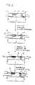
- FIG. 1schematically shown therein in simplified cross-sectional view, is a conventional damascene-type processing sequence employing relatively low cost, high manufacturing throughput plating and CMP techniques for forming recessed “back-end” metallization patterns (illustratively of Cu-based metallurgy but not limited thereto) in a semiconductor device formed in or on a semiconductor wafer substrate 1 .
- the desired arrangement of conductorsis defined as a pattern of recesses 2 such as via holes, grooves, trenches, etc.
- a dielectric layer 3e.g., a silicon oxide and/or nitride or an organic polymeric material
- a layer of Cu or Cu-based alloy 5is deposited by conventional plating techniques, e.g., electroless or electroplating techniques, to fill the recesses 2 .
- the Cu-containing layer 5is deposited as a blanket (or “overburden”) layer of excess thickness t so as to overfill the recesses 2 and cover the upper surface 4 of the dielectric layer 3 .
- the entire excess thickness t of the metal overburden layer 5 over the surface of the dielectric layer 3is removed by a CMP process utilizing an alumina (Al 2 O 3 )-based slurry, leaving metal portions 5 ′ in the recesses 2 with their exposed upper surfaces 6 substantially co-planar with the surface 4 of the dielectric layer 3 .
- the above-described conventional damascene-type processforms in-laid conductors 5 ′ in the dielectric layer 3 while avoiding problems associated with other types of metallization patterning processing, e.g., blanket metal layer deposition, followed by photolithographic masking/etching and dielectric gap filling.
- metallization patterning processinge.g., blanket metal layer deposition
- photolithographic masking/etching and dielectric gap fillinge.g., blanket metal layer deposition
- dielectric gap fillinge.g., blanket metal layer deposition
- single or dual damascene-type processingcan be performed with a variety of other types of substrates, e.g., printed circuit boards, with and/or without intervening dielectric layers, and with a plurality of metallization levels, i.e., five or more levels.
- a drawback associated with Cu-based “back-end” metallizationis the possibility of Cu diffusion into adjacent structures, e.g., an underlying semiconductor substrate (typically Si) or a dielectric layer, resulting in degradation of semiconductive or insulative properties, as well as poor adhesion of the deposited Cu or Cu alloy layer to various materials employed as dielectric inter-layers, etc.
- an adhesion promoting and/or diffusion barrier layerintermediate the semiconductor substrate and the overlying Cu-based metallization layer.
- Suitable materials for such adhesion/barrier layersinclude, e.g., Ti, W, Cr, Ta, and TaN.
- Another drawback associated with the use of Cu or Cu-based metallurgy for “back-end” metallization processing of semiconductor devicesresults from the undesirable formation of copper oxide(s), e.g., Cu 2 O, CuO, CuO 2 , etc., on the planarized Cu or Cu-based alloy surfaces of the in-laid metallization features as a result of oxidation, etc., due to the strong chemical oxidizing agents conventionally included in CMP slurries for enhancing Cu dissolution/removal rates or as a result of exposure of the freshly abraded Cu-based surfaces to an oxidizing atmosphere, e.g., air or oxygen.
- an oxidizing atmospheree.g., air or oxygen.
- the thickness of the copper oxide layercan vary depending upon the particular CMP processing conditions, e.g., stronger oxidizing agents contained in the CMP slurry result in thicker oxide layers, as does increased duration of exposure of freshly abraded, post CMP Cu surfaces to oxidizing atmospheres, e.g., air.
- Such copper oxide-containing layer(s)disadvantageously increase contact resistance and reduce or prevent adhesion of layers thereto, e.g., silicon nitride-based capping layers. Moreover, the copper oxide layers are brittle, increasing the likelihood of circuit disconnect or reduced conductivity due to separation, as by peeling, of the copper oxide layer from conductor layers in contact therewith. Yet another significant disadvantage attributable to the presence of copper oxide at the interface between adjacent electrical conductors results from the rapid diffusion of Cu atoms and/or ions along the oxide layer. The latter characteristic of copper oxide layers disadvantageously results in enhanced material transport during electrical current flow and thus increases the electromigration rate of Cu atoms and/or ions along Cu-based conductor lines.
- Electromigrationoccurs in extended runs or lengths of metal conductor lines carrying significant currents.
- the current flow within the conductor linecan be sufficient to result in movement of metal (Cu) atoms and/or ions along the line via momentum transfer engendered by collision of the metal (Cu) atoms and/or ions with energetic, flowing electrons.
- the current flowalso creates a thermal gradient along the conductor length which increases the mobility of the metal ions and/or atoms.
- metal (Cu) atoms and/or ionsdiffuse in the direction of the current flow, and metal loss at the source end of the conductor eventually results in thinning of the conductor line.
- the electromigration effectcan continue until the conductor line becomes so thin that it separates from the current input or forms an open circuit, resulting in circuit (i.e., semiconductor chip) failure. As this usually occurs over an extended period of operation, the failure is often seen by the end-user.
- An advantage of the present inventionis a method of manufacturing an electrical or electronic device having highly reliable, electromigration-resistant metallization patterns.
- Another advantage of the present inventionis a method of manufacturing a semiconductor integrated circuit device having highly reliable, electromigration-resistant Cu-based metallization patterns.
- Yet another advantage of the present inventionis a method of manufacturing “in-laid”, “damascene”-type Cu-based metallization patterns having improved reliability, high conductivity, and improved electromigration resistance.
- Still another advantage of the present inventionis an improved method of forming high-density, “in-laid” metallization patterns by a “damascene”-type, CMP-based process which is fully compatible with existing process methodology for forming integrated circuit semiconductor devices and printed circuit boards.
- the methodfurther comprises the step of:
- the electrical devicecomprises a semiconductor integrated circuit device
- step (a)comprises providing as the substrate a semiconductor wafer of monocrystalline silicon (Si) or gallium arsenide (GaAs) having a major surface, the dielectric layer is formed over at least a portion of the major surface, the at least one damascene-type, in-laid metal feature comprises a plurality of features of different widths and/or depths for providing vias, inter-level metallization, and/or interconnection lines of at least one active device region or component formed on or within the semiconductor wafer, and the metal of the at least one in-laid metal feature is unalloyed copper (Cu); and step (b) comprises selectively depositing, as by electroless deposition or chemical vapor deposition (CVD), at least one layer comprising at least one metallic passivant element capable of chemically reducing any copper oxide present on the upper surface of the at least one Cu metal feature, the at least one metallic passivant element being selected from the group consist
- step (c)is performed substantially simultaneously with step (b), e.g., at ambient temperatures; whereas according to other embodiments of the present invention, step (c) is performed after step (b), as by annealing in an inert atmosphere; and step (d) comprises selectively removing, as by etching or chemical-mechanical polishing (CMP), any remaining elevated, reacted and/or unreacted portion(s) of the layer comprising at least one metallic passivant element which extend(s) above the upper surface of the layer of dielectric material, thereby making the upper surface of the at least one in-laid metal feature substantially co-planar with the upper surface of the dielectric layer.
- CMPchemical-mechanical polishing
- step (a) for providing the substrate including at least one damascene-type, in-laid metal featurecomprises the preliminary steps of:
- a method of manufacturing a semiconductor integrated circuit devicecomprises the sequential steps of:
- a substratecomprising a semiconductor wafer of monocrystalline Si or GaAs and having a major surface, a dielectric layer formed on at least a portion of the major surface and having an exposed, upper surface, at least one damascene-type, unalloyed Cu metal feature in-laid in the exposed, upper surface of the dielectric layer, the at least one Cu metal feature including an exposed, upper surface substantially co-planar with the exposed, upper surface of the dielectric layer;
- step (a)comprises providing a semiconductor wafer having a dielectric layer on a major surface thereof which comprises a plurality of in-laid, unalloyed Cu metal features of different widths and/or depths for providing vias, inter-level metallization, and/or interconnection lines of at least one active device region or component formed on or within the semiconductor wafer;
- step (b)comprises selectively depositing the at least one layer comprising at least one metallic passivant element by electroless deposition or chemical vapor deposition (CVD); and
- step (c)is performed substantially simultaneously with step (b) at ambient temperature or subsequent to step (b) by annealing at an elevated temperature in an inert atmosphere.
- the methodcomprises the further step of:
- FIG. 1illustrates, in simplified, cross-sectional schematic form, a sequence of processing steps for forming a pattern of damascene-type, in-laid Cu metallization features according to conventional practices for manufacture of semiconductor integrated circuit devices;
- FIG. 2illustrates, in simplified cross-sectional schematic form, a sequence of processing steps for selectively passivating the upper surfaces, i.e., the top interfaces of the pattern of Cu in-laid metallization features of FIG. 1 according to the inventive methodology.
- the present inventionaddresses and solves problems arising from manufacturing electrical devices comprising in-laid metallization patterns, e.g., semiconductor integrated circuit devices, wherein, as part of the fabrication methodology, a plurality of recesses formed in the surface of a dielectric layer overlying a semiconductor substrate comprising at least one active device region or component are filled with a metal, illustratively unalloyed Cu, which is subject to electromigration when the device is in use.
- a metalillustratively unalloyed Cu
- the present inventionenables the formation of in-laid metallization patterns, e.g., of Cu-based metallurgy, in which the tendency for electromigration of the principal metallic element or component is minimized or substantially prevented, and which provide improved adhesion to, and low contact resistance with, adjacent (e.g., overlying) metallization patterns and/or levels in contact therewith.
- in-laid metallization patternse.g., of Cu-based metallurgy
- the present inventionenables the formation of in-laid metallization patterns having passivated upper surfaces (top interfaces) which have little or substantially no tendency for promoting electromigration of atoms and/or ions of the principal underlying metal component and provide improved adhesion with overlying metallization by means of techniques which are fully compatible with the requirements of automated manufacturing technology and product throughput.
- conventional damascene-type methodologysuch as illustrated in FIG.
- a suitable substratee.g., a semiconductor wafer comprising at least one active device region or component, by which processing a metal material, e.g., unalloyed Cu, is utilized for filling the pattern of recesses in the dielectric layer.
- a metal materiale.g., unalloyed Cu
- At least one thin layer comprising at least one passivant element for the metal materiale.g., Cu
- CMPchemical-mechanical polishing
- the passivation reactionmay occur simultaneously with the selective deposition of the at least one thin layer comprising at least one passivant element, i.e., at ambient temperature, or alternatively, may occur subsequent to the selective deposition, as by annealing at an elevated temperature in an inert atmosphere.
- Any elevated, remaining reacted and/or unreacted portion(s) of the at least one thin layer comprising at least one passivant element remaining after reaction/passivation of the upper surface(s), or top interface(s), of the metallization feature(s)is (are) selectively removed, as by CMP, thereby making the exposed, passivated upper surface(s), or top interface(s) of the metallization pattern substantially co-planar with the exposed, upper surface of the dielectric layer.
- a thin layer comprising magnesium (Mg) as passivant elementcan readily reduce CuO 2 typically present on the upper surfaces of unalloyed Cu metallization features.
- the remaining reacted and/or unreacted portions of the passivant layer removed by CMPcomprise Mg and MgO.
- FIG. 2shows, in simplified, cross-sectional, schematic fashion, an illustrative, but not limitative, embodiment of the present invention comprising a sequence of processing steps performed on a semiconductor wafer substrate-based workpiece produced according to the process sequence illustrated in FIG. 1, wherein similar reference numerals are used throughout to denote similar features.
- the inventive processis readily adapted for use in the manufacture of a variety of electrical and electronic devices utilizing in-laid metallization patterns, e.g., printed circuit boards and integrated circuit semiconductor devices. It should also be recognized that the process steps and structures described below do not necessarily form a complete process flow for manufacturing such devices.
- substrateand/or “semiconductor wafer substrate” include, e.g., a semiconductor substrate per se or an epitaxial layer formed on a suitable semiconductor substrate.
- passivant and “passivating element”, as employed herein,refer to elements which are capable of reaction with at least the surface of a metal of an in-laid metallization feature and any oxide(s) of the metal present thereat, as to form a top surface or top interface “passivation layer”, which according to the context of the present invention, refers to an uppermost layer or strata of the metallization feature which effectively reduces electromigration of atoms and/or ions of the principal metallic component of the feature and provides good adhesion and low ohmic electrical resistance with an overlying metallization layer in contact therewith.
- the drawing figures representing cross-sections of portions of a semiconductor device during fabrication processingare not drawn to scale, but instead are drawn as to best illustrate the features of the present invention.
- a semiconductor wafer substrate-based workpiece similar to that shown in the third view of FIG. 1having a desired in-laid metallization pattern, comprising a semiconductor wafer substrate 1 , a dielectric layer 3 overlying substrate 1 and having a pattern of recesses 2 of different widths and/or depths formed in the exposed, upper surface 4 thereof, and a layer 5 of a metal subject to electro-migration, illustratively Cu, filling the recesses 2 , the exposed, upper surfaces 6 of the metal layer 5 being substantially co-planar with the exposed, upper surface 4 of the dielectric layer 3 .
- semiconductor substrate 1typically comprises a wafer of monocrystalline Si or GaAs
- layer 3comprises an insulative material typically utilized as an inter-layer dielectric (“ILD”), i.e., an inorganic material such as a silicon oxide, nitride, or oxynitride, or an organic-based or derived material, such as parylene, benzocyclobutene (BCB), etc.
- ILDinter-layer dielectric
- Recesses 2 formed in the upper, exposed surface 4 of dielectric layer 3are utilized for forming vias, inter-level metallization, and/or interconnection routing of at least one active device region or component formed on or within semiconductor wafer substrate 1 and typically include openings having high aspect (i.e., depth-to-width) ratios greater than one, with sub-micron or micron-sized dimensions, i.e., widths of from about 0.08 to about 3.0 ⁇ m and depths of from about 0.4 to about 2.0 ⁇ m.
- At least one thin layer 7 comprising at least one passivant element (e.g., Ni) for the metal 5 (e.g., unalloyed Cu) of the in-laid metal feature(s) of the metallization patternis selectively deposited on the exposed, upper surface 6 thereof, as by a selective electroless deposition or chemical vapor deposition (CVD) technique.
- a selective electroless deposition or chemical vapor deposition (CVD) techniqueSelectivity of the deposition towards the metal 5 of the metal features may be obtained by use of suitable deposition bath composition in the case of electroless deposition and by appropriate selection of organo-metallic precursor gas(es) in the case of CVD.
- selective electroless deposition of a layer 7 comprising at least one passivant elementfor reducing deleterious oxides and electromigration tendency of unalloyed Cu, e.g., chosen from the group consisting of magnesium (Mg), titanium (Ti), tantalum (Ta), cobalt (Co), nickel (Ni), palladium (Pd), and chromium (Cr), may be obtained by appropriate use of an electroless deposition solution comprising a boride, phosphide, or boride/palladium compound of the metal to be selectively plated on the metal feature(s), whereas selective CVD of the above-enumerated passivant elements may be obtained by use of appropriate organo-metallic precursor gas(es).
- Nibe selectively electrolessly plated on unalloyed Cu metal features from deposition solutions comprising NiB, NiP or NiBPd, or selectively CVD deposited on unalloyed Cu metal features by use of a Ni-based organo-metallic precursor gas.
- suitable electroless deposition bath compositions and/or organo-metallic precursor gases for use with the other enumerated passivant elementscan be determined for use in a particular application.
- the at least one passivant element contained in the at least one thin layer 7must be capable of chemically reducing any oxide(s) of the metal 5 of the metallization feature(s) which are disadvantageously present at the upper surface(s) 6 thereof, e.g., as a result of oxidation by oxidants present in the abrasive slurry employed for the CMP planarization processing, or as a result of exposure to air of the freshly abraded surfaces produced during the CMP.
- the at least one thin layer 7 comprising the at least one passivant elemente.g., Ni or Mg
- the at least one passivant elementmust be of sufficient thickness to provide substantially complete reduction of the oxide layer as well as diffusion of the at least one passivant element into the metal 5 of the metallization feature to a predetermined minimum distance d min. below surface 6 , thereby establishing thereat a passivated surface layer 8 , as shown in the third view of FIG. 2.
- Passivated top surface (or top interface) layer 8forms a new top surface or top interface for subsequent adherent, low ohmic resistance contact with an overlying metallization level, while providing minimal, or substantially no tendency for electromigration of the principal metal 5 (e.g., Cu) of the metallization feature.
- appropriate thicknesses for the at least one alloying element layer 7can be determined and optimized for use in a particular application.
- Layer 7can, depending, inter alia, upon the particular metal 5 of the metallization pattern and choice and number of passivant element(s), comprise a single layer including one passivant element or two or more elements. Alternatively, layer 7 can comprise two or more overlying layers, each including one passivant element. The latter alternative may be preferred when co-deposition of multiple passivant elements in single layer form is impractical or results in poor control of the relative amounts of each passivant element.
- reaction between the at least one passivant element contained in the at least one thin layer 7 to chemically reduce any oxide(s) present at the upper surface 6 of the metal feature(s)can, depending upon the chemical reactivity between the particular passivant element(s) and the particular oxides, occur substantially simultaneously with the deposition of layer 7 , i.e., at the ambient temperature during deposition, or alternatively, subsequently thereto at an elevated temperature, e.g., by annealing in an inert atmosphere.
- copper oxide reductionmay be achieved substantially simultaneously with Ni deposition at ambient temperatures of from about 20 to about 300° C.
- a layer 7 of a less reactive passivant elementsuch as Co
- annealingin an inert atmosphere
- a subsequent annealing treatmentmay be required for formation of diffused layer 8
- reduction of the copper oxides and formation of diffused layer 8can occur substantially simultaneously with diffusion of the passivant element.
- elevated layer portions 7 ′which extend above the level of upper surface 4 of dielectric layer 3 , and composed of reacted and/or unreacted portions of layer(s) 7 (e.g., comprising Mg and/or MgO) may remain on or over passivating surface layer 8 at the upper surface(s) of the metal features after completion of the reaction and diffusion treatment(s).
- layer(s) 7e.g., comprising Mg and/or MgO
- any such remaining layer portion(s) 7 ′is (are) selectively removed, e.g., by etching using an etchant selective against the material of the dielectric layer 3 or by chemical-mechanical planarization (CMP), thereby re-establishing co-planarity of the upper surface 6 of the in-laid metal feature(s) and the upper surface 4 of the dielectric layer 3 .
- CMPchemical-mechanical planarization
- the thus-produced, planarized, in-laid metallization pattern having passivating layer 8 at the upper surfaces (top interfaces) 6 thereof for minimizing or substantially preventing electromigration therefrom and therealongmay then be subjected to further “back-end” metallization processing, as by damascene-type techniques, for forming adherent, low ohmic resistance electrical contact with at least one additional overlying layer of metallization.
- the present inventionthus provides a simple, convenient, and reliable method for reducing, or substantially preventing, deleterious electromigration of metal from in-laid metallization patterns as well as improved adhesion and lower resistance electrical contact thereto, by selectively depositing at least one thin layer comprising at least one passivant element for the metal of the metallization pattern, which at least one passivant element (1) chemically reduces any deleterious oxide layer present at the upper-surfaces of the metallization feature and (2) diffuses into the upper surface thereof to form a passivated top interface.
- the present inventionenables the formation of extremely reliable interconnect members and patterns, illustratively of Cu, but not limited thereto, by providing a method for reliably reducing, or substantially preventing deleterious electromigration, particularly suitable for use in semiconductor “back-end” damascene-type processing, and equally applicable to “dual-damascene”-type processing.
- inventive methodologyenjoys particular utility in the manufacture of semiconductor devices having sub-micron dimensioned metallization features and high aspect ratio openings. Moreover, the inventive method can be practiced at manufacturing rates consistent with the requirements for economic competitiveness, and is fully compatible with conventional process flow for automated manufacture of high-density integration semiconductor devices. In addition, the invention is particularly well suited to the manufacture of circuit boards and other types of electrical and electronic devices and/or components.
Landscapes
- Engineering & Computer Science (AREA)
- Physics & Mathematics (AREA)
- Condensed Matter Physics & Semiconductors (AREA)
- General Physics & Mathematics (AREA)
- Computer Hardware Design (AREA)
- Microelectronics & Electronic Packaging (AREA)
- Power Engineering (AREA)
- Manufacturing & Machinery (AREA)
- Internal Circuitry In Semiconductor Integrated Circuit Devices (AREA)
Abstract
Description
- This application contains subject matter related to subject matter disclosed in co-pending U.S. patent application Ser. No. 09/132,282, filed on Aug. 11, 1998 and Ser. No. 09/225,546, filed on Jan. 5, 1999.[0001]
- The present invention relates to electrical devices, e.g., semiconductor integrated circuit devices, having in-laid ( “damascene”-type) metallization patterns, e.g., interconnection lines, etc., and to a method for minimizing, or substantially preventing, deleterious electromigration of the metallic element(s) of the metallization pattern. More specifically, the present invention relates to semiconductor devices comprising copper (Cu) interconnection patterns and is applicable to manufacture of high speed integrated circuits having sub-micron dimensioned design features and high electrical conductivity interconnect structures.[0002]
- The present invention relates to a method for forming metal films as part of metallization processing of particular utility in the manufacture of electrical and electronic devices, e.g., circuit boards and semiconductor integrated circuits, and is especially adapted for use in processing employing “in-laid” or “damascene”-type technology.[0003]
- The escalating requirements for high density and performance associated with ultra-large scale integration (ULSI) semiconductor device wiring are difficult to satisfy in terms of providing sub-micron-sized (e.g., 0.18 μm and under), low resistance-capacitance (RC) time constant metallization patterns, particularly wherein the sub-micron-sized metallization features, such as vias, contact areas, lines, etc. require grooves, trenches, and other shaped openings or recesses having very high aspect (i.e., depth-to-width) ratios due to microminiaturization.[0004]
- Semiconductor devices of the type contemplated herein typically comprise a semiconductor wafer substrate, usually of doped monocrystalline silicon (Si) or, in some instances, gallium arsenide (GaAs), and a plurality of sequentially formed interlayer dielectrics and electrically conductive patterns formed therein and/or therebetween. An integrated circuit is formed therefrom containing a plurality of patterns of conductive lines separated by inter-wiring spacings, and a plurality of interconnect lines, such as bus lines, bit lines, word lines, and logic interconnect lines. Typically, the conductive patterns of vertically spaced-apart metallization layers or strata are electrically interconnected by a vertically oriented conductive plug filling a via hole formed in the inter-layer dielectric layer separating the layers or strata, while another conductive plug filling a contact area hole establishes electrical contact with an active device region, such as a source/drain region of a transistor, formed in or on the semiconductor substrate. Conductive lines formed in groove- or trench-like openings in overlying inter-layer dielectrics extend substantially parallel to the semiconductor substrate. Semiconductor devices of such type fabricated according to current technology may comprise five or more layers or strata of such metallization in order to satisfy device geometry and microminiaturization requirements.[0005]
- Electrically conductive films or layers of the type contemplated for use in e.g., “back-end” semiconductor manufacturing technology for fabricating devices having multi-level metallization patterns such as described supra, typically comprise a metal such as titanium (Ti), tantalum (Ta), tungsten (W), aluminum (Al), chromium (Cr), nickel (Ni), cobalt (Co), silver (Ag), gold (Au), copper (Cu) and their alloys. In use, each of the enumerated metals presents advantages as well as drawbacks. For example, Al is relatively inexpensive, exhibits low resistivity, and is relatively easy to etch. However, in addition to being difficult to deposit by lower cost, lower temperature, more rapid “wet” type technology such as electrodeposition, step coverage with Al is poor when the metallization features are scale down to sub-micron size, resulting in decreased reliability of interconnections, high current densities at certain locations, and increased electro-migration. In addition, certain low dielectric constant materials, e.g., polyimides, when employed as dielectric inter-layers, create moisture/bias reliability problems when in contact with Al.[0006]
- Copper (Cu) and Cu-based alloys are particularly attractive for use in large scale integration (LSI), very large-scale integration (VLSI), and ultra-large scale (ULSI) semiconductor devices requiring multi-level metallization systems for “back-end” processing of the semiconductor wafers on which the devices are based. Cu- and Cu alloy-based metallization systems have very low resistivities, i.e., significantly lower than that of W and even lower than those of previously preferred systems utilizing Al and its alloys, as well as a higher (but not complete) resistance to electromigration. Moreover, Cu and its alloys enjoy a considerable cost advantage over a number of the above-enumerated metals, notably Ag and Au. Also, in contrast to Al and the refractory-type metals (e.g., Ti, Ta, and W), Cu and its alloys can be readily deposited at low temperatures in good quality, bright layer form by well-known “wet” plating techniques, such as electroless and electroplating techniques, at deposition rates fully compatible with the requirements of device manufacturing throughput.[0007]
- Electroless plating of Cu generally involves the controlled auto-catalytic deposition of a continuous film of Cu or an alloy thereof on a catalytic surface by the interaction of at least a Cu-containing salt and a chemical reducing agent contained in a suitable solution, whereas electroplating comprises employing electrons supplied to an electrode (comprising the surface(s) to be plated) from an external source (i.e., a power supply) for reducing Cu ions in solution and depositing reduced Cu metal atoms on the plating surface(s). In either case, a nucleation/seed layer is required for catalysis and/or deposition on the types of substrates contemplated herein. Finally, while electroplating requires a continuous nucleation/seed layer, very thin and discontinuous islands of a catalytic metal may be employed with electroless plating.[0008]
- As indicated above, a commonly employed method for forming “in-laid” metallization patterns as are required for “back-end” metallization processing of semiconductor wafers employs “damascene”-type technology. Generally, in such processing methodology, a recess (i.e., an opening) for forming, e.g., a via hole in a dielectric layer for electrically connecting vertically separated metallization layers, or a groove or trench for a metallization line, is created in the dielectric layer by conventional photolithographic and etching techniques, and filled with a selected metal. Any excess metal overfilling the recess and/or extending over the surface of the dielectric layer is then removed by, e.g., chemical-mechanical polishing (CMP), wherein a moving pad is biased against the surface to be polished/planarized, with the interposition of a slurry containing abrasive particles (and other ingredients) therebetween.[0009]
- A variant of the above-described technique, termed “dual damascene” processing, involves the formation of an opening comprising a lower contact or via hole section in communication with an upper groove or trench section, which opening is filled with a conductive material, typically a metal, to simultaneously form a conductive via plug in electrical contact with a conductive line.[0010]
- Referring now to FIG. 1, schematically shown therein in simplified cross-sectional view, is a conventional damascene-type processing sequence employing relatively low cost, high manufacturing throughput plating and CMP techniques for forming recessed “back-end” metallization patterns (illustratively of Cu-based metallurgy but not limited thereto) in a semiconductor device formed in or on a[0011]
semiconductor wafer substrate 1. In a first step, the desired arrangement of conductors is defined as a pattern ofrecesses 2 such as via holes, grooves, trenches, etc. formed (as by conventional photolithographic and etching techniques) in thesurface 4 of a dielectric layer3 (e.g., a silicon oxide and/or nitride or an organic polymeric material) deposited or otherwise formed over thesemiconductor substrate 1. In a second step, a layer of Cu or Cu-basedalloy 5 is deposited by conventional plating techniques, e.g., electroless or electroplating techniques, to fill therecesses 2. In order to ensure complete filling of the recesses, the Cu-containinglayer 5 is deposited as a blanket (or “overburden”) layer of excess thickness t so as to overfill therecesses 2 and cover theupper surface 4 of thedielectric layer 3. Next, the entire excess thickness t of the metaloverburden layer 5 over the surface of thedielectric layer 3 is removed by a CMP process utilizing an alumina (Al2O3)-based slurry, leavingmetal portions 5′ in therecesses 2 with their exposedupper surfaces 6 substantially co-planar with thesurface 4 of thedielectric layer 3. - The above-described conventional damascene-type process forms in-[0012]
laid conductors 5′ in thedielectric layer 3 while avoiding problems associated with other types of metallization patterning processing, e.g., blanket metal layer deposition, followed by photolithographic masking/etching and dielectric gap filling. In addition, such single or dual damascene-type processing can be performed with a variety of other types of substrates, e.g., printed circuit boards, with and/or without intervening dielectric layers, and with a plurality of metallization levels, i.e., five or more levels. - A drawback associated with Cu-based “back-end” metallization is the possibility of Cu diffusion into adjacent structures, e.g., an underlying semiconductor substrate (typically Si) or a dielectric layer, resulting in degradation of semiconductive or insulative properties, as well as poor adhesion of the deposited Cu or Cu alloy layer to various materials employed as dielectric inter-layers, etc. As a consequence of these phenomena associated with Cu-based metallurgy, it is generally necessary to provide an adhesion promoting and/or diffusion barrier layer intermediate the semiconductor substrate and the overlying Cu-based metallization layer. Suitable materials for such adhesion/barrier layers include, e.g., Ti, W, Cr, Ta, and TaN.[0013]
- Another drawback associated with the use of Cu or Cu-based metallurgy for “back-end” metallization processing of semiconductor devices, results from the undesirable formation of copper oxide(s), e.g., Cu[0014]2O, CuO, CuO2, etc., on the planarized Cu or Cu-based alloy surfaces of the in-laid metallization features as a result of oxidation, etc., due to the strong chemical oxidizing agents conventionally included in CMP slurries for enhancing Cu dissolution/removal rates or as a result of exposure of the freshly abraded Cu-based surfaces to an oxidizing atmosphere, e.g., air or oxygen. The thickness of the copper oxide layer can vary depending upon the particular CMP processing conditions, e.g., stronger oxidizing agents contained in the CMP slurry result in thicker oxide layers, as does increased duration of exposure of freshly abraded, post CMP Cu surfaces to oxidizing atmospheres, e.g., air.
- Such copper oxide-containing layer(s) disadvantageously increase contact resistance and reduce or prevent adhesion of layers thereto, e.g., silicon nitride-based capping layers. Moreover, the copper oxide layers are brittle, increasing the likelihood of circuit disconnect or reduced conductivity due to separation, as by peeling, of the copper oxide layer from conductor layers in contact therewith. Yet another significant disadvantage attributable to the presence of copper oxide at the interface between adjacent electrical conductors results from the rapid diffusion of Cu atoms and/or ions along the oxide layer. The latter characteristic of copper oxide layers disadvantageously results in enhanced material transport during electrical current flow and thus increases the electromigration rate of Cu atoms and/or ions along Cu-based conductor lines.[0015]
- Electromigration occurs in extended runs or lengths of metal conductor lines carrying significant currents. According to a conventional theory for explaining the mechanism of electromigration, the current flow within the conductor line can be sufficient to result in movement of metal (Cu) atoms and/or ions along the line via momentum transfer engendered by collision of the metal (Cu) atoms and/or ions with energetic, flowing electrons. The current flow also creates a thermal gradient along the conductor length which increases the mobility of the metal ions and/or atoms. As a consequence of the momentum transfer and the thermally enhanced mobility, metal (Cu) atoms and/or ions diffuse in the direction of the current flow, and metal loss at the source end of the conductor eventually results in thinning of the conductor line. The electromigration effect can continue until the conductor line becomes so thin that it separates from the current input or forms an open circuit, resulting in circuit (i.e., semiconductor chip) failure. As this usually occurs over an extended period of operation, the failure is often seen by the end-user.[0016]
- As design rules for high integration density, high speed semiconductor devices extend deeper into the sub-micron range, e.g., about 0.18 μm and under, e.g., about 0.15 μm and below, and the number of metallization levels increases, the reliability of the “back-end” interconnection patterns and systems become particularly critical for the obtainment of desired operating characteristics and performance.[0017]
- Thus, there exists a need for metallization process methodology which avoids the above-mentioned drawbacks associated with oxide layer formation, electromigration, etc., and which enables formation of metallization members, e.g., interconnect and routing lines, particularly of Cu or Cu-based alloys, having high reliability, high product yield, improved electromigration resistance, and high performance. In particular, there exists a need for eliminating the problems associated with electromigration and oxide layer formation resulting from CMP processing to form “in-laid”, “damascene-type” Cu-based metallization patterns. Moreover, there exists a need for improved metallization processing technology which is fully compatible with conventional process flow, methodology, and throughput requirements in the manufacture of integrated circuit semiconductor devices and other devices requiring “in-laid” metallization patterns.[0018]
- An advantage of the present invention is a method of manufacturing an electrical or electronic device having highly reliable, electromigration-resistant metallization patterns.[0019]
- Another advantage of the present invention is a method of manufacturing a semiconductor integrated circuit device having highly reliable, electromigration-resistant Cu-based metallization patterns.[0020]
- Yet another advantage of the present invention is a method of manufacturing “in-laid”, “damascene”-type Cu-based metallization patterns having improved reliability, high conductivity, and improved electromigration resistance.[0021]
- Still another advantage of the present invention is an improved method of forming high-density, “in-laid” metallization patterns by a “damascene”-type, CMP-based process which is fully compatible with existing process methodology for forming integrated circuit semiconductor devices and printed circuit boards.[0022]
- Additional advantages and other features of the present invention will be set forth in the description which follows and in part will become apparent to those having ordinary skill in the art upon examination of the following or will be learned from the practice of the invention. The advantages of the present invention may be realized and obtained as particularly pointed out in the appended claims.[0023]
- According to one aspect of the present invention, the foregoing and other advantages are achieved in part by a method of manufacturing an electrical device, the method comprising the sequential steps of:[0024]
- (a) providing a substrate including at least one damascene-type, metal feature in-laid in the upper, exposed surface of a layer of dielectric material overlying at least a portion of the substrate, the at least one metal feature including an upper, exposed surface substantially co-planar with the upper surface of the layer of dielectric material;[0025]
- (b) selectively depositing on the exposed upper surface of the at least one metal feature at least one layer comprising at least one metallic passivant element for passivating the upper surface of the at least one metal feature; and[0026]
- (c) effecting reaction between at least a portion of the at least one layer comprising at least one metallic passivant element and the upper surface of the at least one metal feature to form a passivating layer thereat, whereby electromigration of the metal of the at least one metal feature is minimized or substantially prevented.[0027]
- According to embodiments of the present invention, the method further comprises the step of:[0028]
- (d) selectively removing any remaining reacted and/or unreacted portion(s) of the at least one layer comprising at least one metallic passivant element which extend(s) above the upper surface of the layer of dielectric material, thereby making the upper surface of the at least one in-laid metal feature substantially co-planar with the upper surface of the layer of dielectric material.[0029]
- In accordance with embodiments of the present invention, the electrical device comprises a semiconductor integrated circuit device, and step (a) comprises providing as the substrate a semiconductor wafer of monocrystalline silicon (Si) or gallium arsenide (GaAs) having a major surface, the dielectric layer is formed over at least a portion of the major surface, the at least one damascene-type, in-laid metal feature comprises a plurality of features of different widths and/or depths for providing vias, inter-level metallization, and/or interconnection lines of at least one active device region or component formed on or within the semiconductor wafer, and the metal of the at least one in-laid metal feature is unalloyed copper (Cu); and step (b) comprises selectively depositing, as by electroless deposition or chemical vapor deposition (CVD), at least one layer comprising at least one metallic passivant element capable of chemically reducing any copper oxide present on the upper surface of the at least one Cu metal feature, the at least one metallic passivant element being selected from the group consisting of: magnesium (Mg), titanium (Ti), tantalum (Ta), cobalt (Co), nickel (Ni), palladium (Pd) and chromium (Cr).[0030]
- In embodiments according to the present invention, step (c) is performed substantially simultaneously with step (b), e.g., at ambient temperatures; whereas according to other embodiments of the present invention, step (c) is performed after step (b), as by annealing in an inert atmosphere; and step (d) comprises selectively removing, as by etching or chemical-mechanical polishing (CMP), any remaining elevated, reacted and/or unreacted portion(s) of the layer comprising at least one metallic passivant element which extend(s) above the upper surface of the layer of dielectric material, thereby making the upper surface of the at least one in-laid metal feature substantially co-planar with the upper surface of the dielectric layer.[0031]
- According to further embodiments of the present invention, step (a) for providing the substrate including at least one damascene-type, in-laid metal feature comprises the preliminary steps of:[0032]
- i. forming a dielectric layer on a surface of a substrate, the dielectric layer having an exposed, upper surface;[0033]
- ii. forming at least one recess in the exposed, upper surface of the dielectric layer;[0034]
- iii. depositing a metal layer filling the at least one recess and extending over the upper surface of the dielectric layer;[0035]
- iv. removing the portion(s) of the metal layer extending over the upper surface of the dielectric layer; and[0036]
- v. removing (e.g., by CMP) any excess thickness portion(s) of the metal layer filling the at least one recess which extend(s) above the upper surface of the dielectric layer, thereby making the upper, exposed, upper surface of the at least one in-laid metal feature substantially co-planar with the exposed, upper surface of the dielectric layer.[0037]
- According to another aspect of the present invention, a method of manufacturing a semiconductor integrated circuit device comprises the sequential steps of:[0038]
- (a) providing a substrate comprising a semiconductor wafer of monocrystalline Si or GaAs and having a major surface, a dielectric layer formed on at least a portion of the major surface and having an exposed, upper surface, at least one damascene-type, unalloyed Cu metal feature in-laid in the exposed, upper surface of the dielectric layer, the at least one Cu metal feature including an exposed, upper surface substantially co-planar with the exposed, upper surface of the dielectric layer;[0039]
- (b) selectively depositing at least one layer comprising at least one metallic passivant element for the Cu metal feature on the upper surface of the at least one Cu metal feature, the at least one metallic passivant element being capable of chemically reducing any copper oxide present on the upper surface of the at least one metal feature and selected from the group consisting of: magnesium (Mg), titanium (Ti), tantalum (Ta), cobalt (Co), nickel (Ni), palladium (Pd), and chromium (Cr); and[0040]
- (c) effecting reaction between at least a portion of the at least one layer comprising at least one metallic passivant element and the upper surface of the at least one Cu metal feature to form a passivating layer thereat, whereby electromigration of Cu atoms and/or ions from the at least one Cu metal feature is minimized or substantially prevented.[0041]
- According to embodiments of the present invention:[0042]
- step (a) comprises providing a semiconductor wafer having a dielectric layer on a major surface thereof which comprises a plurality of in-laid, unalloyed Cu metal features of different widths and/or depths for providing vias, inter-level metallization, and/or interconnection lines of at least one active device region or component formed on or within the semiconductor wafer;[0043]
- step (b) comprises selectively depositing the at least one layer comprising at least one metallic passivant element by electroless deposition or chemical vapor deposition (CVD); and[0044]
- step (c) is performed substantially simultaneously with step (b) at ambient temperature or subsequent to step (b) by annealing at an elevated temperature in an inert atmosphere.[0045]
- According to still further embodiments of the present invention, the method comprises the further step of:[0046]
- (d) selectively removing any elevated, remaining reacted and/or unreacted portion(s) of the at least one layer comprising at least one metallic passivating element which extend(s) above the upper surface of the layer of dielectric material, thereby making the upper surface of the at least one in-laid, Cu metal feature substantially co-planar with the upper surface of the dielectric layer.[0047]
- Additional advantages of the present invention will readily become apparent to those skilled in the art from the following detailed description, wherein only the preferred embodiment of the present invention is shown and described, simply by way of illustration of the best mode contemplated for carrying out the method of the present invention. As will be understood, the present invention is capable of other and different embodiments, and its several details are capable of modification in various obvious respects, all without departing from the present invention. Accordingly, the drawing and description are to be regarded as illustrative in nature, and not as limitative.[0048]
- The following detailed description of an embodiment of the present invention can best be understood when read in conjunction with the following drawings, in which like reference numerals are employed throughout to designate similar features, wherein:[0049]
- FIG. 1 illustrates, in simplified, cross-sectional schematic form, a sequence of processing steps for forming a pattern of damascene-type, in-laid Cu metallization features according to conventional practices for manufacture of semiconductor integrated circuit devices; and[0050]
- FIG. 2 illustrates, in simplified cross-sectional schematic form, a sequence of processing steps for selectively passivating the upper surfaces, i.e., the top interfaces of the pattern of Cu in-laid metallization features of FIG. 1 according to the inventive methodology.[0051]
- The present invention addresses and solves problems arising from manufacturing electrical devices comprising in-laid metallization patterns, e.g., semiconductor integrated circuit devices, wherein, as part of the fabrication methodology, a plurality of recesses formed in the surface of a dielectric layer overlying a semiconductor substrate comprising at least one active device region or component are filled with a metal, illustratively unalloyed Cu, which is subject to electromigration when the device is in use. More specifically, the present invention enables the formation of in-laid metallization patterns, e.g., of Cu-based metallurgy, in which the tendency for electromigration of the principal metallic element or component is minimized or substantially prevented, and which provide improved adhesion to, and low contact resistance with, adjacent (e.g., overlying) metallization patterns and/or levels in contact therewith.[0052]
- The present invention enables the formation of in-laid metallization patterns having passivated upper surfaces (top interfaces) which have little or substantially no tendency for promoting electromigration of atoms and/or ions of the principal underlying metal component and provide improved adhesion with overlying metallization by means of techniques which are fully compatible with the requirements of automated manufacturing technology and product throughput. Briefly stated, according to the present invention, conventional damascene-type methodology (such as illustrated in FIG. 1) is employed for forming an in-laid metallization pattern in a dielectric layer overlying a suitable substrate, e.g., a semiconductor wafer comprising at least one active device region or component, by which processing a metal material, e.g., unalloyed Cu, is utilized for filling the pattern of recesses in the dielectric layer. Subsequent to planarization processing, as by chemical-mechanical polishing (CMP), at least one thin layer comprising at least one passivant element for the metal material, e.g., Cu, is selectively deposited on the exposed, upper surface(s) of the feature(s) of the metallization pattern, and reaction between the at least one passivant element and the upper surface(s) of the metal of the in-laid metallization feature(s) is effected for selectively forming a passivating layer thereat, the passivation reaction including reduction of any deleterious oxide of the metal of the metallization feature(s) present at the upper surface(s) thereof. The passivation reaction may occur simultaneously with the selective deposition of the at least one thin layer comprising at least one passivant element, i.e., at ambient temperature, or alternatively, may occur subsequent to the selective deposition, as by annealing at an elevated temperature in an inert atmosphere. Any elevated, remaining reacted and/or unreacted portion(s) of the at least one thin layer comprising at least one passivant element remaining after reaction/passivation of the upper surface(s), or top interface(s), of the metallization feature(s) is (are) selectively removed, as by CMP, thereby making the exposed, passivated upper surface(s), or top interface(s) of the metallization pattern substantially co-planar with the exposed, upper surface of the dielectric layer. By way of example, but not limitation, a thin layer comprising magnesium (Mg) as passivant element can readily reduce CuO[0053]2typically present on the upper surfaces of unalloyed Cu metallization features. In such instance, the remaining reacted and/or unreacted portions of the passivant layer removed by CMP comprise Mg and MgO.
- An embodiment of the present invention will now be described with reference to FIG. 2, which shows, in simplified, cross-sectional, schematic fashion, an illustrative, but not limitative, embodiment of the present invention comprising a sequence of processing steps performed on a semiconductor wafer substrate-based workpiece produced according to the process sequence illustrated in FIG. 1, wherein similar reference numerals are used throughout to denote similar features. As will be apparent to one of ordinary skill in the art, the inventive process is readily adapted for use in the manufacture of a variety of electrical and electronic devices utilizing in-laid metallization patterns, e.g., printed circuit boards and integrated circuit semiconductor devices. It should also be recognized that the process steps and structures described below do not necessarily form a complete process flow for manufacturing such devices. However, the present invention can be used in conjunction with conventional technology currently employed in the art, e.g., integrated circuit fabrication methodology, and, consequently, only so much of the commonly practiced process steps are included here as are necessary for an understanding of the present invention. As employed throughout the present disclosure and claims, the terms “substrate” and/or “semiconductor wafer substrate” include, e.g., a semiconductor substrate per se or an epitaxial layer formed on a suitable semiconductor substrate. The expressions “passivant” and “passivating element”, as employed herein, refer to elements which are capable of reaction with at least the surface of a metal of an in-laid metallization feature and any oxide(s) of the metal present thereat, as to form a top surface or top interface “passivation layer”, which according to the context of the present invention, refers to an uppermost layer or strata of the metallization feature which effectively reduces electromigration of atoms and/or ions of the principal metallic component of the feature and provides good adhesion and low ohmic electrical resistance with an overlying metallization layer in contact therewith. Finally, the drawing figures representing cross-sections of portions of a semiconductor device during fabrication processing are not drawn to scale, but instead are drawn as to best illustrate the features of the present invention.[0054]
- Referring now to the first view shown in FIG. 2, in a preliminary step according to the present invention, a semiconductor wafer substrate-based workpiece similar to that shown in the third view of FIG. 1 is provided, having a desired in-laid metallization pattern, comprising a[0055]
semiconductor wafer substrate 1, adielectric layer 3overlying substrate 1 and having a pattern ofrecesses 2 of different widths and/or depths formed in the exposed,upper surface 4 thereof, and alayer 5 of a metal subject to electro-migration, illustratively Cu, filling therecesses 2, the exposed,upper surfaces 6 of themetal layer 5 being substantially co-planar with the exposed,upper surface 4 of thedielectric layer 3. - In the illustrated structure,[0056]
semiconductor substrate 1 typically comprises a wafer of monocrystalline Si or GaAs,layer 3 comprises an insulative material typically utilized as an inter-layer dielectric (“ILD”), i.e., an inorganic material such as a silicon oxide, nitride, or oxynitride, or an organic-based or derived material, such as parylene, benzocyclobutene (BCB), etc.Recesses 2 formed in the upper, exposedsurface 4 ofdielectric layer 3 are utilized for forming vias, inter-level metallization, and/or interconnection routing of at least one active device region or component formed on or withinsemiconductor wafer substrate 1 and typically include openings having high aspect (i.e., depth-to-width) ratios greater than one, with sub-micron or micron-sized dimensions, i.e., widths of from about 0.08 to about 3.0 μm and depths of from about 0.4 to about 2.0 μm. - Referring now to the second view shown in FIG. 2, in a first step according to the inventive methodology, at least one[0057]
thin layer 7 comprising at least one passivant element (e.g., Ni) for the metal5 (e.g., unalloyed Cu) of the in-laid metal feature(s) of the metallization pattern is selectively deposited on the exposed,upper surface 6 thereof, as by a selective electroless deposition or chemical vapor deposition (CVD) technique. Selectivity of the deposition towards themetal 5 of the metal features may be obtained by use of suitable deposition bath composition in the case of electroless deposition and by appropriate selection of organo-metallic precursor gas(es) in the case of CVD. For example, selective electroless deposition of alayer 7 comprising at least one passivant element, for reducing deleterious oxides and electromigration tendency of unalloyed Cu, e.g., chosen from the group consisting of magnesium (Mg), titanium (Ti), tantalum (Ta), cobalt (Co), nickel (Ni), palladium (Pd), and chromium (Cr), may be obtained by appropriate use of an electroless deposition solution comprising a boride, phosphide, or boride/palladium compound of the metal to be selectively plated on the metal feature(s), whereas selective CVD of the above-enumerated passivant elements may be obtained by use of appropriate organo-metallic precursor gas(es). By way of illustration, but not limitation, Ni be selectively electrolessly plated on unalloyed Cu metal features from deposition solutions comprising NiB, NiP or NiBPd, or selectively CVD deposited on unalloyed Cu metal features by use of a Ni-based organo-metallic precursor gas. Given the present disclosure and objectives of the invention, suitable electroless deposition bath compositions and/or organo-metallic precursor gases for use with the other enumerated passivant elements can be determined for use in a particular application. - According to an essential feature of the present invention, the at least one passivant element contained in the at least one[0058]
thin layer 7 must be capable of chemically reducing any oxide(s) of themetal 5 of the metallization feature(s) which are disadvantageously present at the upper surface(s)6 thereof, e.g., as a result of oxidation by oxidants present in the abrasive slurry employed for the CMP planarization processing, or as a result of exposure to air of the freshly abraded surfaces produced during the CMP. By way of illustration, but not limitation, in the illustrated case where unalloyed Cu (e.g., electroplated)metal 5 is utilized for forming the metallization pattern, such deleterious copper oxides include Cu2O, CuO, and CuO2. As a consequence of the above requirement, the at least onethin layer 7 comprising the at least one passivant element (e.g., Ni or Mg) must be of sufficient thickness to provide substantially complete reduction of the oxide layer as well as diffusion of the at least one passivant element into themetal 5 of the metallization feature to a predetermined minimum distance dmin.belowsurface 6, thereby establishing thereat a passivatedsurface layer 8, as shown in the third view of FIG. 2. Passivated top surface (or top interface)layer 8, according to the invention, forms a new top surface or top interface for subsequent adherent, low ohmic resistance contact with an overlying metallization level, while providing minimal, or substantially no tendency for electromigration of the principal metal5 (e.g., Cu) of the metallization feature. Given the present disclosure and objectives of the invention, appropriate thicknesses for the at least onealloying element layer 7, as well as minimum diffusion depth dmin., can be determined and optimized for use in a particular application. - [0059]
Layer 7 can, depending, inter alia, upon theparticular metal 5 of the metallization pattern and choice and number of passivant element(s), comprise a single layer including one passivant element or two or more elements. Alternatively,layer 7 can comprise two or more overlying layers, each including one passivant element. The latter alternative may be preferred when co-deposition of multiple passivant elements in single layer form is impractical or results in poor control of the relative amounts of each passivant element. - According to another feature of the present invention, reaction between the at least one passivant element contained in the at least one[0060]
thin layer 7 to chemically reduce any oxide(s) present at theupper surface 6 of the metal feature(s) can, depending upon the chemical reactivity between the particular passivant element(s) and the particular oxides, occur substantially simultaneously with the deposition oflayer 7, i.e., at the ambient temperature during deposition, or alternatively, subsequently thereto at an elevated temperature, e.g., by annealing in an inert atmosphere. By way of illustration, but not limitation, in the case of alayer 7 of Ni as passivant element and unalloyed Cu asmetal 5 of the metallization feature(s), copper oxide reduction may be achieved substantially simultaneously with Ni deposition at ambient temperatures of from about 20 to about 300° C., whereas with alayer 7 of a less reactive passivant element, such as Co, annealing (in an inert atmosphere) at a temperature of from about 200 to about 450° C. for from about 30 sec. to about 60 min. is necessary to effect copper oxide reduction. In the former case of reaction at ambient temperature, however, a subsequent annealing treatment, as indicated in the third view of FIG. 2, may be required for formation of diffusedlayer 8, whereas, in the latter case, where reaction requires elevated temperature, reduction of the copper oxides and formation of diffusedlayer 8 can occur substantially simultaneously with diffusion of the passivant element. - Referring now to the final view illustrated in FIG. 2,[0061]
elevated layer portions 7′ which extend above the level ofupper surface 4 ofdielectric layer 3, and composed of reacted and/or unreacted portions of layer(s)7 (e.g., comprising Mg and/or MgO) may remain on or overpassivating surface layer 8 at the upper surface(s) of the metal features after completion of the reaction and diffusion treatment(s). In the next step according to the inventive methodology, any such remaining layer portion(s)7′ is (are) selectively removed, e.g., by etching using an etchant selective against the material of thedielectric layer 3 or by chemical-mechanical planarization (CMP), thereby re-establishing co-planarity of theupper surface 6 of the in-laid metal feature(s) and theupper surface 4 of thedielectric layer 3. The thus-produced, planarized, in-laid metallization pattern havingpassivating layer 8 at the upper surfaces (top interfaces)6 thereof for minimizing or substantially preventing electromigration therefrom and therealong may then be subjected to further “back-end” metallization processing, as by damascene-type techniques, for forming adherent, low ohmic resistance electrical contact with at least one additional overlying layer of metallization. - The present invention thus provides a simple, convenient, and reliable method for reducing, or substantially preventing, deleterious electromigration of metal from in-laid metallization patterns as well as improved adhesion and lower resistance electrical contact thereto, by selectively depositing at least one thin layer comprising at least one passivant element for the metal of the metallization pattern, which at least one passivant element (1) chemically reduces any deleterious oxide layer present at the upper-surfaces of the metallization feature and (2) diffuses into the upper surface thereof to form a passivated top interface. The present invention enables the formation of extremely reliable interconnect members and patterns, illustratively of Cu, but not limited thereto, by providing a method for reliably reducing, or substantially preventing deleterious electromigration, particularly suitable for use in semiconductor “back-end” damascene-type processing, and equally applicable to “dual-damascene”-type processing.[0062]
- The inventive methodology enjoys particular utility in the manufacture of semiconductor devices having sub-micron dimensioned metallization features and high aspect ratio openings. Moreover, the inventive method can be practiced at manufacturing rates consistent with the requirements for economic competitiveness, and is fully compatible with conventional process flow for automated manufacture of high-density integration semiconductor devices. In addition, the invention is particularly well suited to the manufacture of circuit boards and other types of electrical and electronic devices and/or components.[0063]
- In the previous description, numerous specific details are set forth, such as specific materials, structures, reactants, processes, etc. in order to provide a better understanding of the present invention. However, the present invention can be practiced without resorting to the details specifically set forth. In other instances, well known processing materials and techniques have not been described in detail in order not to unnecessarily obscure the present invention.[0064]
- Only the preferred embodiment of the present invention and but a few examples of its versatility are shown and described in the present disclosure. It is to be understood that the present invention is capable of use in various other combinations and environments and is susceptible of changes or modifications within the scope of the inventive concept as expressed herein.[0065]
Claims (20)
Priority Applications (1)
| Application Number | Priority Date | Filing Date | Title |
|---|---|---|---|
| US09/484,412US6455425B1 (en) | 2000-01-18 | 2000-01-18 | Selective deposition process for passivating top interface of damascene-type Cu interconnect lines |
Applications Claiming Priority (1)
| Application Number | Priority Date | Filing Date | Title |
|---|---|---|---|
| US09/484,412US6455425B1 (en) | 2000-01-18 | 2000-01-18 | Selective deposition process for passivating top interface of damascene-type Cu interconnect lines |
Publications (2)
| Publication Number | Publication Date |
|---|---|
| US20020027261A1true US20020027261A1 (en) | 2002-03-07 |
| US6455425B1 US6455425B1 (en) | 2002-09-24 |
Family
ID=23924072
Family Applications (1)
| Application Number | Title | Priority Date | Filing Date |
|---|---|---|---|
| US09/484,412Expired - LifetimeUS6455425B1 (en) | 2000-01-18 | 2000-01-18 | Selective deposition process for passivating top interface of damascene-type Cu interconnect lines |
Country Status (1)
| Country | Link |
|---|---|
| US (1) | US6455425B1 (en) |
Cited By (40)
| Publication number | Priority date | Publication date | Assignee | Title |
|---|---|---|---|---|
| US20020084529A1 (en)* | 2000-12-28 | 2002-07-04 | Dubin Valery M. | Interconnect structures and a method of electroless introduction of interconnect structures |
| WO2003094209A3 (en)* | 2002-05-03 | 2004-08-05 | Intel Corp | Use of conductive electrolessly deposided etch stop layers, liner layers and via plugs in interconnect structures |
| US20050101130A1 (en)* | 2003-11-07 | 2005-05-12 | Applied Materials, Inc. | Method and tool of chemical doping CoW alloys with Re for increasing barrier properties of electroless capping layers for IC Cu interconnects |
| US20060146233A1 (en)* | 2004-12-30 | 2006-07-06 | Magnachip Semiconductor Ltd. | Image sensor with enlarged photo detection area and method for fabricating the same |
| US7087104B2 (en) | 2003-06-26 | 2006-08-08 | Intel Corporation | Preparation of electroless deposition solutions |
| US20080254314A1 (en)* | 2004-08-30 | 2008-10-16 | Russell Stephen W | Methods for forming an enriched metal oxide surface |
| US7573133B2 (en) | 2003-12-09 | 2009-08-11 | Uri Cohen | Interconnect structures and methods for their fabrication |
| US7709958B2 (en) | 2004-06-18 | 2010-05-04 | Uri Cohen | Methods and structures for interconnect passivation |
| US20110086314A1 (en)* | 2004-07-29 | 2011-04-14 | Rohm And Haas Electronic Material Llc | Melts |
| US20130089979A1 (en)* | 2008-03-19 | 2013-04-11 | National University Corporation Tohoku University | Semiconductor device having a multilevel interconnect structure and method for fabricating the same |
| US20140083753A1 (en)* | 2011-03-24 | 2014-03-27 | Fujifilm Corporation | Method of forming copper wiring, method of manufacturing wiring board, and wiring board |
| US20150170961A1 (en)* | 2013-12-18 | 2015-06-18 | Patricio E. Romero | Selective area deposition of metal films by atomic layer deposition (ald) and chemical vapor deposition (cvd) |
| WO2015088899A1 (en)* | 2013-12-09 | 2015-06-18 | Applied Materials, Inc. | Methods of selective layer deposition |
| US20150325511A1 (en)* | 2013-03-14 | 2015-11-12 | UTAC Headquarters Pte. Ltd. | Semiconductor packages and methods of packaging semiconductor devices |
| US9514933B2 (en) | 2014-01-05 | 2016-12-06 | Applied Materials, Inc. | Film deposition using spatial atomic layer deposition or pulsed chemical vapor deposition |
| US20170323776A1 (en)* | 2016-05-05 | 2017-11-09 | Asm Ip Holding B.V. | Selective deposition using hydrophobic precursors |
| US10428421B2 (en) | 2015-08-03 | 2019-10-01 | Asm Ip Holding B.V. | Selective deposition on metal or metallic surfaces relative to dielectric surfaces |
| US10443123B2 (en) | 2014-04-16 | 2019-10-15 | Asm Ip Holding B.V. | Dual selective deposition |
| US10456808B2 (en) | 2014-02-04 | 2019-10-29 | Asm Ip Holding B.V. | Selective deposition of metals, metal oxides, and dielectrics |
| US10480064B2 (en) | 2016-06-08 | 2019-11-19 | Asm Ip Holding B.V. | Reaction chamber passivation and selective deposition of metallic films |
| US10566185B2 (en) | 2015-08-05 | 2020-02-18 | Asm Ip Holding B.V. | Selective deposition of aluminum and nitrogen containing material |
| US10741411B2 (en) | 2015-02-23 | 2020-08-11 | Asm Ip Holding B.V. | Removal of surface passivation |
| US10872765B2 (en) | 2018-05-02 | 2020-12-22 | Asm Ip Holding B.V. | Selective layer formation using deposition and removing |
| US10900120B2 (en) | 2017-07-14 | 2021-01-26 | Asm Ip Holding B.V. | Passivation against vapor deposition |
| US10903113B2 (en) | 2015-08-05 | 2021-01-26 | Asm Ip Holding B.V. | Selective deposition of aluminum and nitrogen containing material |
| US10923361B2 (en) | 2016-06-01 | 2021-02-16 | Asm Ip Holding B.V. | Deposition of organic films |
| US11056385B2 (en) | 2011-12-09 | 2021-07-06 | Asm International N.V. | Selective formation of metallic films on metallic surfaces |
| US11094535B2 (en) | 2017-02-14 | 2021-08-17 | Asm Ip Holding B.V. | Selective passivation and selective deposition |
| US11139163B2 (en) | 2019-10-31 | 2021-10-05 | Asm Ip Holding B.V. | Selective deposition of SiOC thin films |
| US11145506B2 (en) | 2018-10-02 | 2021-10-12 | Asm Ip Holding B.V. | Selective passivation and selective deposition |
| US11170993B2 (en) | 2017-05-16 | 2021-11-09 | Asm Ip Holding B.V. | Selective PEALD of oxide on dielectric |
| US11387107B2 (en) | 2016-06-01 | 2022-07-12 | Asm Ip Holding B.V. | Deposition of organic films |
| US11389824B2 (en) | 2015-10-09 | 2022-07-19 | Asm Ip Holding B.V. | Vapor phase deposition of organic films |
| US11430656B2 (en) | 2016-11-29 | 2022-08-30 | Asm Ip Holding B.V. | Deposition of oxide thin films |
| US11446699B2 (en) | 2015-10-09 | 2022-09-20 | Asm Ip Holding B.V. | Vapor phase deposition of organic films |
| US11501965B2 (en) | 2017-05-05 | 2022-11-15 | Asm Ip Holding B.V. | Plasma enhanced deposition processes for controlled formation of metal oxide thin films |
| US11608557B2 (en) | 2020-03-30 | 2023-03-21 | Asm Ip Holding B.V. | Simultaneous selective deposition of two different materials on two different surfaces |
| US11643720B2 (en) | 2020-03-30 | 2023-05-09 | Asm Ip Holding B.V. | Selective deposition of silicon oxide on metal surfaces |
| US11898240B2 (en) | 2020-03-30 | 2024-02-13 | Asm Ip Holding B.V. | Selective deposition of silicon oxide on dielectric surfaces relative to metal surfaces |
| US11965238B2 (en) | 2019-04-12 | 2024-04-23 | Asm Ip Holding B.V. | Selective deposition of metal oxides on metal surfaces |
Families Citing this family (22)
| Publication number | Priority date | Publication date | Assignee | Title |
|---|---|---|---|---|
| JP2002367998A (en)* | 2001-06-11 | 2002-12-20 | Ebara Corp | Semiconductor device and manufacturing method therefor |
| US6884724B2 (en)* | 2001-08-24 | 2005-04-26 | Applied Materials, Inc. | Method for dishing reduction and feature passivation in polishing processes |
| US6706630B1 (en)* | 2003-02-28 | 2004-03-16 | Advanced Micro Devices, Inc. | Method for forming an alloyed metal conductive element of an integrated circuit |
| US6927113B1 (en) | 2003-05-23 | 2005-08-09 | Advanced Micro Devices | Semiconductor component and method of manufacture |
| US7186637B2 (en)* | 2003-07-31 | 2007-03-06 | Intel Corporation | Method of bonding semiconductor devices |
| US7268074B2 (en)* | 2004-06-14 | 2007-09-11 | Enthone, Inc. | Capping of metal interconnects in integrated circuit electronic devices |
| SG120200A1 (en) | 2004-08-27 | 2006-03-28 | Micron Technology Inc | Slanted vias for electrical circuits on circuit boards and other substrates |
| US20060216929A1 (en)* | 2005-03-28 | 2006-09-28 | Hyun-Mog Park | Etch stopless dual damascene structure and method of fabrication |
| US7795134B2 (en) | 2005-06-28 | 2010-09-14 | Micron Technology, Inc. | Conductive interconnect structures and formation methods using supercritical fluids |
| US7262134B2 (en) | 2005-09-01 | 2007-08-28 | Micron Technology, Inc. | Microfeature workpieces and methods for forming interconnects in microfeature workpieces |
| US7863187B2 (en) | 2005-09-01 | 2011-01-04 | Micron Technology, Inc. | Microfeature workpieces and methods for forming interconnects in microfeature workpieces |
| US20070045120A1 (en)* | 2005-09-01 | 2007-03-01 | Micron Technology, Inc. | Methods and apparatus for filling features in microfeature workpieces |
| US7902643B2 (en) | 2006-08-31 | 2011-03-08 | Micron Technology, Inc. | Microfeature workpieces having interconnects and conductive backplanes, and associated systems and methods |
| US7884015B2 (en) | 2007-12-06 | 2011-02-08 | Micron Technology, Inc. | Methods for forming interconnects in microelectronic workpieces and microelectronic workpieces formed using such methods |
| US20090194846A1 (en)* | 2008-02-02 | 2009-08-06 | Edward Yi Chang | Fully Cu-metallized III-V group compound semiconductor device with palladium/germanium/copper ohmic contact system |
| US7968460B2 (en)* | 2008-06-19 | 2011-06-28 | Micron Technology, Inc. | Semiconductor with through-substrate interconnect |
| US9799562B2 (en) | 2009-08-21 | 2017-10-24 | Micron Technology, Inc. | Vias and conductive routing layers in semiconductor substrates |
| US8907457B2 (en)* | 2010-02-08 | 2014-12-09 | Micron Technology, Inc. | Microelectronic devices with through-substrate interconnects and associated methods of manufacturing |
| JP5451547B2 (en)* | 2010-07-09 | 2014-03-26 | キヤノン株式会社 | Solid-state imaging device |
| US8951911B2 (en)* | 2011-03-31 | 2015-02-10 | Applied Materials, Inc. | Process for damascene structure with reduced low-k damage |
| US20150206798A1 (en)* | 2014-01-17 | 2015-07-23 | Taiwan Semiconductor Manufacturing Company, Ltd. | Interconnect Structure And Method of Forming |
| US11426818B2 (en) | 2018-08-10 | 2022-08-30 | The Research Foundation for the State University | Additive manufacturing processes and additively manufactured products |
Family Cites Families (16)
| Publication number | Priority date | Publication date | Assignee | Title |
|---|---|---|---|---|
| US4335506A (en) | 1980-08-04 | 1982-06-22 | International Business Machines Corporation | Method of forming aluminum/copper alloy conductors |
| US4789648A (en) | 1985-10-28 | 1988-12-06 | International Business Machines Corporation | Method for producing coplanar multi-level metal/insulator films on a substrate and for forming patterned conductive lines simultaneously with stud vias |
| JP2885616B2 (en) | 1992-07-31 | 1999-04-26 | 株式会社東芝 | Semiconductor device and manufacturing method thereof |
| US5730809A (en)* | 1994-11-09 | 1998-03-24 | Enthone-Omi, Inc. | Passivate for tungsten alloy electroplating |
| KR100413890B1 (en) | 1995-03-02 | 2004-03-19 | 동경 엘렉트론 주식회사 | Manufacturing method and manufacturing apparatus of semiconductor device |
| US5969422A (en)* | 1997-05-15 | 1999-10-19 | Advanced Micro Devices, Inc. | Plated copper interconnect structure |
| US6069068A (en)* | 1997-05-30 | 2000-05-30 | International Business Machines Corporation | Sub-quarter-micron copper interconnections with improved electromigration resistance and reduced defect sensitivity |
| US6077780A (en)* | 1997-12-03 | 2000-06-20 | Advanced Micro Devices, Inc. | Method for filling high aspect ratio openings of an integrated circuit to minimize electromigration failure |
| US6022808A (en) | 1998-03-16 | 2000-02-08 | Advanced Micro Devices, Inc. | Copper interconnect methodology for enhanced electromigration resistance |
| US5968333A (en)* | 1998-04-07 | 1999-10-19 | Advanced Micro Devices, Inc. | Method of electroplating a copper or copper alloy interconnect |
| US6147000A (en)* | 1998-08-11 | 2000-11-14 | Advanced Micro Devices, Inc. | Method for forming low dielectric passivation of copper interconnects |
| US6172421B1 (en)* | 1998-08-11 | 2001-01-09 | Advanced Micro Devices, Inc. | Semiconductor device having an intermetallic layer on metal interconnects |
| JP3379575B2 (en)* | 1998-11-19 | 2003-02-24 | 日本電気株式会社 | Cu wiring forming method |
| US20020001954A1 (en)* | 1999-06-02 | 2002-01-03 | Shih-Ying Hsu | Dual damascene process |
| US6251786B1 (en)* | 1999-09-07 | 2001-06-26 | Chartered Semiconductor Manufacturing Ltd. | Method to create a copper dual damascene structure with less dishing and erosion |
| US6319819B1 (en)* | 2000-01-18 | 2001-11-20 | Advanced Micro Devices, Inc. | Process for passivating top interface of damascene-type Cu interconnect lines |
- 2000
- 2000-01-18USUS09/484,412patent/US6455425B1/ennot_activeExpired - Lifetime
Cited By (82)
| Publication number | Priority date | Publication date | Assignee | Title |
|---|---|---|---|---|
| US6977224B2 (en) | 2000-12-28 | 2005-12-20 | Intel Corporation | Method of electroless introduction of interconnect structures |
| US20020084529A1 (en)* | 2000-12-28 | 2002-07-04 | Dubin Valery M. | Interconnect structures and a method of electroless introduction of interconnect structures |
| US6958547B2 (en) | 2002-05-03 | 2005-10-25 | Intel Corporation | Interconnect structures containing conductive electrolessly deposited etch stop layers, liner layers, and via plugs |
| US7008872B2 (en) | 2002-05-03 | 2006-03-07 | Intel Corporation | Use of conductive electrolessly deposited etch stop layers, liner layers and via plugs in interconnect structures |
| WO2003094209A3 (en)* | 2002-05-03 | 2004-08-05 | Intel Corp | Use of conductive electrolessly deposided etch stop layers, liner layers and via plugs in interconnect structures |
| US7087104B2 (en) | 2003-06-26 | 2006-08-08 | Intel Corporation | Preparation of electroless deposition solutions |
| US20050101130A1 (en)* | 2003-11-07 | 2005-05-12 | Applied Materials, Inc. | Method and tool of chemical doping CoW alloys with Re for increasing barrier properties of electroless capping layers for IC Cu interconnects |
| US7205233B2 (en) | 2003-11-07 | 2007-04-17 | Applied Materials, Inc. | Method for forming CoWRe alloys by electroless deposition |
| US7573133B2 (en) | 2003-12-09 | 2009-08-11 | Uri Cohen | Interconnect structures and methods for their fabrication |
| US7709958B2 (en) | 2004-06-18 | 2010-05-04 | Uri Cohen | Methods and structures for interconnect passivation |
| US20100213614A1 (en)* | 2004-06-18 | 2010-08-26 | Uri Cohen | Methods for Passivating Metallic Interconnects |
| US20110086314A1 (en)* | 2004-07-29 | 2011-04-14 | Rohm And Haas Electronic Material Llc | Melts |
| US20080254314A1 (en)* | 2004-08-30 | 2008-10-16 | Russell Stephen W | Methods for forming an enriched metal oxide surface |
| US8568900B2 (en)* | 2004-08-30 | 2013-10-29 | Micron Technology, Inc. | Methods for forming an enriched metal oxide surface |
| US7495206B2 (en)* | 2004-12-30 | 2009-02-24 | Magnachip Semiconductor, Ltd. | Image sensor with stacked and bonded photo detection and peripheral circuit substrates |
| US20060146233A1 (en)* | 2004-12-30 | 2006-07-06 | Magnachip Semiconductor Ltd. | Image sensor with enlarged photo detection area and method for fabricating the same |
| US20130089979A1 (en)* | 2008-03-19 | 2013-04-11 | National University Corporation Tohoku University | Semiconductor device having a multilevel interconnect structure and method for fabricating the same |
| US8709939B2 (en)* | 2008-03-19 | 2014-04-29 | Semiconductor Technology Academic Research Center | Semiconductor device having a multilevel interconnect structure and method for fabricating the same |
| US20140083753A1 (en)* | 2011-03-24 | 2014-03-27 | Fujifilm Corporation | Method of forming copper wiring, method of manufacturing wiring board, and wiring board |
| US11056385B2 (en) | 2011-12-09 | 2021-07-06 | Asm International N.V. | Selective formation of metallic films on metallic surfaces |
| US9786625B2 (en)* | 2013-03-14 | 2017-10-10 | United Test And Assembly Center Ltd. | Semiconductor packages and methods of packaging semiconductor devices |
| US20150325511A1 (en)* | 2013-03-14 | 2015-11-12 | UTAC Headquarters Pte. Ltd. | Semiconductor packages and methods of packaging semiconductor devices |
| US9716012B2 (en) | 2013-12-09 | 2017-07-25 | Applied Materials, Inc. | Methods of selective layer deposition |
| WO2015088899A1 (en)* | 2013-12-09 | 2015-06-18 | Applied Materials, Inc. | Methods of selective layer deposition |
| US20160086850A1 (en)* | 2013-12-18 | 2016-03-24 | Patricio E. Romero | Selective area deposition of metal films by atomic layer deposition (ald) and chemical vapor deposition (cvd) |
| US9583389B2 (en)* | 2013-12-18 | 2017-02-28 | Intel Corporation | Selective area deposition of metal films by atomic layer deposition (ALD) and chemical vapor deposition (CVD) |
| US9236292B2 (en)* | 2013-12-18 | 2016-01-12 | Intel Corporation | Selective area deposition of metal films by atomic layer deposition (ALD) and chemical vapor deposition (CVD) |
| US20150170961A1 (en)* | 2013-12-18 | 2015-06-18 | Patricio E. Romero | Selective area deposition of metal films by atomic layer deposition (ald) and chemical vapor deposition (cvd) |
| US9514933B2 (en) | 2014-01-05 | 2016-12-06 | Applied Materials, Inc. | Film deposition using spatial atomic layer deposition or pulsed chemical vapor deposition |
| US10456808B2 (en) | 2014-02-04 | 2019-10-29 | Asm Ip Holding B.V. | Selective deposition of metals, metal oxides, and dielectrics |
| US11975357B2 (en) | 2014-02-04 | 2024-05-07 | Asm Ip Holding B.V. | Selective deposition of metals, metal oxides, and dielectrics |
| US11213853B2 (en) | 2014-02-04 | 2022-01-04 | Asm Ip Holding B.V. | Selective deposition of metals, metal oxides, and dielectrics |
| US10443123B2 (en) | 2014-04-16 | 2019-10-15 | Asm Ip Holding B.V. | Dual selective deposition |
| US11525184B2 (en) | 2014-04-16 | 2022-12-13 | Asm Ip Holding B.V. | Dual selective deposition |
| US11047040B2 (en) | 2014-04-16 | 2021-06-29 | Asm Ip Holding B.V. | Dual selective deposition |
| US11062914B2 (en) | 2015-02-23 | 2021-07-13 | Asm Ip Holding B.V. | Removal of surface passivation |
| US10741411B2 (en) | 2015-02-23 | 2020-08-11 | Asm Ip Holding B.V. | Removal of surface passivation |
| US10428421B2 (en) | 2015-08-03 | 2019-10-01 | Asm Ip Holding B.V. | Selective deposition on metal or metallic surfaces relative to dielectric surfaces |
| US11174550B2 (en) | 2015-08-03 | 2021-11-16 | Asm Ip Holding B.V. | Selective deposition on metal or metallic surfaces relative to dielectric surfaces |
| US10847361B2 (en) | 2015-08-05 | 2020-11-24 | Asm Ip Holding B.V. | Selective deposition of aluminum and nitrogen containing material |
| US10903113B2 (en) | 2015-08-05 | 2021-01-26 | Asm Ip Holding B.V. | Selective deposition of aluminum and nitrogen containing material |
| US10566185B2 (en) | 2015-08-05 | 2020-02-18 | Asm Ip Holding B.V. | Selective deposition of aluminum and nitrogen containing material |
| US11446699B2 (en) | 2015-10-09 | 2022-09-20 | Asm Ip Holding B.V. | Vapor phase deposition of organic films |
| US12134108B2 (en) | 2015-10-09 | 2024-11-05 | Asm Ip Holding B.V. | Vapor phase deposition of organic films |
| US12138654B2 (en) | 2015-10-09 | 2024-11-12 | Asm Ip Holding B.V. | Vapor phase deposition of organic films |
| US11389824B2 (en) | 2015-10-09 | 2022-07-19 | Asm Ip Holding B.V. | Vapor phase deposition of organic films |
| US11654454B2 (en) | 2015-10-09 | 2023-05-23 | Asm Ip Holding B.V. | Vapor phase deposition of organic films |
| KR20170125740A (en)* | 2016-05-05 | 2017-11-15 | 에이에스엠 아이피 홀딩 비.브이. | Selective deposition using hydrophobic precursors |
| US20170323776A1 (en)* | 2016-05-05 | 2017-11-09 | Asm Ip Holding B.V. | Selective deposition using hydrophobic precursors |
| US11081342B2 (en)* | 2016-05-05 | 2021-08-03 | Asm Ip Holding B.V. | Selective deposition using hydrophobic precursors |
| US12080548B2 (en) | 2016-05-05 | 2024-09-03 | Asm Ip Holding B.V. | Selective deposition using hydrophobic precursors |
| KR102377746B1 (en) | 2016-05-05 | 2022-03-23 | 에이에스엠 아이피 홀딩 비.브이. | Selective deposition using hydrophobic precursors |
| US10923361B2 (en) | 2016-06-01 | 2021-02-16 | Asm Ip Holding B.V. | Deposition of organic films |
| US11387107B2 (en) | 2016-06-01 | 2022-07-12 | Asm Ip Holding B.V. | Deposition of organic films |
| US11728175B2 (en) | 2016-06-01 | 2023-08-15 | Asm Ip Holding B.V. | Deposition of organic films |
| US12300505B2 (en) | 2016-06-01 | 2025-05-13 | Asm Ip Holding B.V. | Deposition of organic films |
| US12205820B2 (en) | 2016-06-01 | 2025-01-21 | Asm Ip Holding B.V. | Deposition of organic films |
| US10480064B2 (en) | 2016-06-08 | 2019-11-19 | Asm Ip Holding B.V. | Reaction chamber passivation and selective deposition of metallic films |
| US10793946B1 (en) | 2016-06-08 | 2020-10-06 | Asm Ip Holding B.V. | Reaction chamber passivation and selective deposition of metallic films |
| US12154785B2 (en) | 2016-11-29 | 2024-11-26 | Asm Ip Holding B.V. | Deposition of oxide thin films |
| US11430656B2 (en) | 2016-11-29 | 2022-08-30 | Asm Ip Holding B.V. | Deposition of oxide thin films |
| US12170197B2 (en) | 2017-02-14 | 2024-12-17 | Asm Ip Holding B.V. | Selective passivation and selective deposition |
| US11094535B2 (en) | 2017-02-14 | 2021-08-17 | Asm Ip Holding B.V. | Selective passivation and selective deposition |
| US11501965B2 (en) | 2017-05-05 | 2022-11-15 | Asm Ip Holding B.V. | Plasma enhanced deposition processes for controlled formation of metal oxide thin films |
| US11728164B2 (en) | 2017-05-16 | 2023-08-15 | Asm Ip Holding B.V. | Selective PEALD of oxide on dielectric |
| US11170993B2 (en) | 2017-05-16 | 2021-11-09 | Asm Ip Holding B.V. | Selective PEALD of oxide on dielectric |
| US10900120B2 (en) | 2017-07-14 | 2021-01-26 | Asm Ip Holding B.V. | Passivation against vapor deposition |
| US11396701B2 (en) | 2017-07-14 | 2022-07-26 | Asm Ip Holding B.V. | Passivation against vapor deposition |
| US11739422B2 (en) | 2017-07-14 | 2023-08-29 | Asm Ip Holding B.V. | Passivation against vapor deposition |
| US10872765B2 (en) | 2018-05-02 | 2020-12-22 | Asm Ip Holding B.V. | Selective layer formation using deposition and removing |
| US11804373B2 (en) | 2018-05-02 | 2023-10-31 | ASM IP Holding, B.V. | Selective layer formation using deposition and removing |
| US11501966B2 (en) | 2018-05-02 | 2022-11-15 | Asm Ip Holding B.V. | Selective layer formation using deposition and removing |
| US11830732B2 (en) | 2018-10-02 | 2023-11-28 | Asm Ip Holding B.V. | Selective passivation and selective deposition |
| US11145506B2 (en) | 2018-10-02 | 2021-10-12 | Asm Ip Holding B.V. | Selective passivation and selective deposition |
| US12322593B2 (en) | 2018-10-02 | 2025-06-03 | Asm Ip Holding B.V. | Selective passivation and selective deposition |
| US11965238B2 (en) | 2019-04-12 | 2024-04-23 | Asm Ip Holding B.V. | Selective deposition of metal oxides on metal surfaces |
| US12068156B2 (en) | 2019-10-31 | 2024-08-20 | Asm Ip Holding B.V. | Selective deposition of SiOC thin films |
| US11664219B2 (en) | 2019-10-31 | 2023-05-30 | Asm Ip Holding B.V. | Selective deposition of SiOC thin films |
| US11139163B2 (en) | 2019-10-31 | 2021-10-05 | Asm Ip Holding B.V. | Selective deposition of SiOC thin films |
| US11898240B2 (en) | 2020-03-30 | 2024-02-13 | Asm Ip Holding B.V. | Selective deposition of silicon oxide on dielectric surfaces relative to metal surfaces |
| US11643720B2 (en) | 2020-03-30 | 2023-05-09 | Asm Ip Holding B.V. | Selective deposition of silicon oxide on metal surfaces |
| US11608557B2 (en) | 2020-03-30 | 2023-03-21 | Asm Ip Holding B.V. | Simultaneous selective deposition of two different materials on two different surfaces |
Also Published As
| Publication number | Publication date |
|---|---|
| US6455425B1 (en) | 2002-09-24 |
Similar Documents
| Publication | Publication Date | Title |
|---|---|---|
| US6455425B1 (en) | Selective deposition process for passivating top interface of damascene-type Cu interconnect lines | |
| US6444567B1 (en) | Process for alloying damascene-type Cu interconnect lines | |
| US6319819B1 (en) | Process for passivating top interface of damascene-type Cu interconnect lines | |
| US5824599A (en) | Protected encapsulation of catalytic layer for electroless copper interconnect | |
| US6249055B1 (en) | Self-encapsulated copper metallization | |
| US6147000A (en) | Method for forming low dielectric passivation of copper interconnects | |
| US6350687B1 (en) | Method of fabricating improved copper metallization including forming and removing passivation layer before forming capping film | |
| US6117782A (en) | Optimized trench/via profile for damascene filling | |
| US6174812B1 (en) | Copper damascene technology for ultra large scale integration circuits | |
| US6211071B1 (en) | Optimized trench/via profile for damascene filling | |
| US6303505B1 (en) | Copper interconnect with improved electromigration resistance | |
| US5969422A (en) | Plated copper interconnect structure | |
| US6316359B1 (en) | Interconnect structure in a semiconductor device and method of formation | |
| EP2020027B1 (en) | Structure and method for creating reliable via contacts for interconnect applications | |
| US6242349B1 (en) | Method of forming copper/copper alloy interconnection with reduced electromigration | |
| US6979625B1 (en) | Copper interconnects with metal capping layer and selective copper alloys | |
| US6121150A (en) | Sputter-resistant hardmask for damascene trench/via formation | |
| US6022808A (en) | Copper interconnect methodology for enhanced electromigration resistance | |
| US6528884B1 (en) | Conformal atomic liner layer in an integrated circuit interconnect | |
| US6821879B2 (en) | Copper interconnect by immersion/electroless plating in dual damascene process | |
| US6121149A (en) | Optimized trench/via profile for damascene filling | |
| US20020089063A1 (en) | Copper dual damascene interconnect technology | |
| US6165894A (en) | Method of reliably capping copper interconnects | |
| US7879720B2 (en) | Methods of forming electrical interconnects using electroless plating techniques that inhibit void formation | |
| US6410418B1 (en) | Recess metallization via selective insulator formation on nucleation/seed layer |
Legal Events
| Date | Code | Title | Description |
|---|---|---|---|
| AS | Assignment | Owner name:ADVANCED MICRO DEVICES, INC., CALIFORNIA Free format text:ASSIGNMENT OF ASSIGNORS INTEREST;ASSIGNORS:BESSER, PAUL R.;ERB, DARRELL M.;LOPATIN, SERGEY;REEL/FRAME:010585/0794;SIGNING DATES FROM 19991102 TO 20000112 | |
| STCF | Information on status: patent grant | Free format text:PATENTED CASE | |
| FPAY | Fee payment | Year of fee payment:4 | |
| AS | Assignment | Owner name:GLOBALFOUNDRIES INC., CAYMAN ISLANDS Free format text:AFFIRMATION OF PATENT ASSIGNMENT;ASSIGNOR:ADVANCED MICRO DEVICES, INC.;REEL/FRAME:023119/0083 Effective date:20090630 Owner name:GLOBALFOUNDRIES INC., CAYMAN ISLANDS Free format text:AFFIRMATION OF PATENT ASSIGNMENT;ASSIGNOR:ADVANCED MICRO DEVICES, INC.;REEL/FRAME:023120/0426 Effective date:20090630 Owner name:GLOBALFOUNDRIES INC.,CAYMAN ISLANDS Free format text:AFFIRMATION OF PATENT ASSIGNMENT;ASSIGNOR:ADVANCED MICRO DEVICES, INC.;REEL/FRAME:023120/0426 Effective date:20090630 | |
| FPAY | Fee payment | Year of fee payment:8 | |
| FPAY | Fee payment | Year of fee payment:12 | |
| AS | Assignment | Owner name:TESSERA ADVANCED TECHNOLOGIES, INC., CALIFORNIA Free format text:ASSIGNMENT OF ASSIGNORS INTEREST;ASSIGNOR:GLOBALFOUNDRIES INC.;REEL/FRAME:047039/0957 Effective date:20180925 |