US20020025665A1 - Method of forming a metal to polysilicon contact in oxygen environment - Google Patents
Method of forming a metal to polysilicon contact in oxygen environmentDownload PDFInfo
- Publication number
- US20020025665A1 US20020025665A1US09/930,268US93026801AUS2002025665A1US 20020025665 A1US20020025665 A1US 20020025665A1US 93026801 AUS93026801 AUS 93026801AUS 2002025665 A1US2002025665 A1US 2002025665A1
- Authority
- US
- United States
- Prior art keywords
- layer
- metal
- conductive layer
- polysilicon
- contact
- Prior art date
- Legal status (The legal status is an assumption and is not a legal conclusion. Google has not performed a legal analysis and makes no representation as to the accuracy of the status listed.)
- Granted
Links
Images


Classifications
- H—ELECTRICITY
- H01—ELECTRIC ELEMENTS
- H01L—SEMICONDUCTOR DEVICES NOT COVERED BY CLASS H10
- H01L21/00—Processes or apparatus adapted for the manufacture or treatment of semiconductor or solid state devices or of parts thereof
- H01L21/70—Manufacture or treatment of devices consisting of a plurality of solid state components formed in or on a common substrate or of parts thereof; Manufacture of integrated circuit devices or of parts thereof
- H01L21/71—Manufacture of specific parts of devices defined in group H01L21/70
- H01L21/768—Applying interconnections to be used for carrying current between separate components within a device comprising conductors and dielectrics
- H01L21/76838—Applying interconnections to be used for carrying current between separate components within a device comprising conductors and dielectrics characterised by the formation and the after-treatment of the conductors
- H01L21/76841—Barrier, adhesion or liner layers
- H01L21/7687—Thin films associated with contacts of capacitors
- H—ELECTRICITY
- H01—ELECTRIC ELEMENTS
- H01L—SEMICONDUCTOR DEVICES NOT COVERED BY CLASS H10
- H01L21/00—Processes or apparatus adapted for the manufacture or treatment of semiconductor or solid state devices or of parts thereof
- H01L21/70—Manufacture or treatment of devices consisting of a plurality of solid state components formed in or on a common substrate or of parts thereof; Manufacture of integrated circuit devices or of parts thereof
- H01L21/71—Manufacture of specific parts of devices defined in group H01L21/70
- H01L21/768—Applying interconnections to be used for carrying current between separate components within a device comprising conductors and dielectrics
- H01L21/76801—Applying interconnections to be used for carrying current between separate components within a device comprising conductors and dielectrics characterised by the formation and the after-treatment of the dielectrics, e.g. smoothing
- H01L21/76802—Applying interconnections to be used for carrying current between separate components within a device comprising conductors and dielectrics characterised by the formation and the after-treatment of the dielectrics, e.g. smoothing by forming openings in dielectrics
- H—ELECTRICITY
- H01—ELECTRIC ELEMENTS
- H01L—SEMICONDUCTOR DEVICES NOT COVERED BY CLASS H10
- H01L21/00—Processes or apparatus adapted for the manufacture or treatment of semiconductor or solid state devices or of parts thereof
- H01L21/70—Manufacture or treatment of devices consisting of a plurality of solid state components formed in or on a common substrate or of parts thereof; Manufacture of integrated circuit devices or of parts thereof
- H01L21/71—Manufacture of specific parts of devices defined in group H01L21/70
- H01L21/768—Applying interconnections to be used for carrying current between separate components within a device comprising conductors and dielectrics
- H01L21/76801—Applying interconnections to be used for carrying current between separate components within a device comprising conductors and dielectrics characterised by the formation and the after-treatment of the dielectrics, e.g. smoothing
- H01L21/76829—Applying interconnections to be used for carrying current between separate components within a device comprising conductors and dielectrics characterised by the formation and the after-treatment of the dielectrics, e.g. smoothing characterised by the formation of thin functional dielectric layers, e.g. dielectric etch-stop, barrier, capping or liner layers
- H01L21/76831—Applying interconnections to be used for carrying current between separate components within a device comprising conductors and dielectrics characterised by the formation and the after-treatment of the dielectrics, e.g. smoothing characterised by the formation of thin functional dielectric layers, e.g. dielectric etch-stop, barrier, capping or liner layers in via holes or trenches, e.g. non-conductive sidewall liners
- H—ELECTRICITY
- H01—ELECTRIC ELEMENTS
- H01L—SEMICONDUCTOR DEVICES NOT COVERED BY CLASS H10
- H01L21/00—Processes or apparatus adapted for the manufacture or treatment of semiconductor or solid state devices or of parts thereof
- H01L21/70—Manufacture or treatment of devices consisting of a plurality of solid state components formed in or on a common substrate or of parts thereof; Manufacture of integrated circuit devices or of parts thereof
- H01L21/71—Manufacture of specific parts of devices defined in group H01L21/70
- H01L21/768—Applying interconnections to be used for carrying current between separate components within a device comprising conductors and dielectrics
- H01L21/76838—Applying interconnections to be used for carrying current between separate components within a device comprising conductors and dielectrics characterised by the formation and the after-treatment of the conductors
- H01L21/76877—Filling of holes, grooves or trenches, e.g. vias, with conductive material
Definitions
- the present inventionrelates to the field of semiconductor integrated circuits and, in particular, to metal-polysilicon contacts capable of tolerating high temperature oxidizing environments.
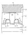
- FIG. 1depicts a portion of a conventional memory cell construction for a DRAM at an intermediate stage of the fabrication, in which a metal-polysilicon contact is formed according to conventional processes.
- a pair of memory cells having respective access transistors 33are formed within a well 13 of a substrate 12 .
- the wells and transistorsare surrounded by a field oxide region 14 that provides isolation.
- N-type active regions 16are provided in the doped p-type well 13 of substrate 12 (for NMOS transistors) and the pair of access transistors have respective gate stacks 30 .
- the gate stacks 30include an oxide layer 18 , a conductive layer 20 , such as poly silicon, nitride spacers 32 , and a nitride cap 22 .
- Additional stacks 31may also be formed for use in performing self aligned contact etches to form conductive plugs for capacitor structures in the region between stacks 30 , 31 . The details of these steps are well-known in the art and are not described in this application.
- a polysilicon plug 50(FIG. 1) is formed in a contact opening of a first insulating layer 24 , to directly connect to a source or drain region 16 of the semiconductor device.
- the first insulating layer 24could be, for example, borophosphosilicate glass (BPSG), borosilicate glass (BSG), or phosphosilicate glass (PSG).
- BPSGborophosphosilicate glass
- BSGborosilicate glass
- PSGphosphosilicate glass
- a second insulating layer 25which can be of the same material as that of the first insulating layer 24 , is deposited over the first insulating layer 24 and the polysilicon plug 50 .
- a contact opening or viais etched over the polysilicon plug 50 and a metal layer or metal electrode 55 is then deposited and patterned to connect to the polysilicon plug 50 , as illustrated in FIG. 1.
- polysilicon plug 50comes into contact with the metal layer or electrode 55 at a metal-polysilicon interface 51 (FIG. 1).
- any other conductorsuch as a capacitor plate for example, may also be in contact with a polysilicon plug, and the discussion herein applies to any metal-polysilicon interface.
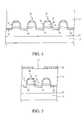
- barrier layershave been introduced to solve the silicon diffusion problem at the metal-polysilicon contact, such as interface 51 (FIG. 1).
- a barrier layer 52is illustrated in FIG. 2 (which shows only a middle portion of the structure of FIG. 1).
- the barrier layeris a refractory metal compound such as refractory metal nitrides (for example TiN or HfN), refractory metal carbides (for example TiC or WC), or refractory metal borides (for example TiB or MoB).
- Barrier layerssuppress the diffusion of the silicon and metal atoms at the polysilicon-metal interface, while offering a low resistivity and low contact resistance between the silicon and the barrier layer, and between the metal and the barrier layer.
- barrier layersin that, in an O 2 high temperature environment, they oxidize and disconnect the metal layer from the polysilicon plug.
- the oxide of the barrier layermay be formed either between the metal and the barrier layer, or between the polysilicon and the barrier layer. The latter situation is illustrated in FIG. 3, which shows metal oxide layer 53 formed between barrier layer 52 and polysilicon plug 50 . In either case, the oxide of the barrier layer affects the conductive properties of the metal contact by increasing the electric resistance in the electrical connection region.
- barrier layersFor further improve the characteristics of the barrier layers, certain metals, for which both the oxidized species (MeO) as well as the unoxidized species (Me) are electrically conducting, have been recently used as barrier layers between metal and polysilicon. Examples of these metals are ruthenium (Ru), platinum (Pt), or iridium (Ir), among others. Since these barrier layers are conductive in both the metal and the oxide forms, this approach is useful in that both the oxide and the metal forms slow down the oxidation front in an O 2 high temperature environment. However, this technique has a drawback in that there will still be some areas where the metal does not oxidize and, thus, the barrier layer would consist of portions of pure metal species and portions of metal oxide.
- the present inventionprovides a method for forming a metal-polysilicon contact that would be capable of tolerating an O 2 environment up to several hundred degrees Celsius for several hours.
- the metal filmis surrounded by a plurality of oxygen sinks. These oxygen sinks are oxidized before the metal film at the bottom of the plug is oxidized. Accordingly, the conductive connection between the polysilicon and any device built on top of the barrier layer is preserved.
- FIG. 3is a schematic cross-sectional view of the FIG. 2 device depicting the formation of an oxide layer between a polysilicon plug and a barrier layer.
- FIG. 4is a schematic cross-sectional view of a portion of a memory DRAM device, in which a metal-polysilicon contact according to a first embodiment and method of the present invention will be formed.
- FIG. 5is a schematic cross sectional view of the FIG. 4 device at a stage of processing subsequent to that shown in FIG. 4.
- FIG. 8is a schematic cross sectional view of the FIG. 7 device at a stage of processing subsequent to that shown in FIG. 7.
- FIG. 10is a schematic cross sectional view of the FIG. 9 device at a stage of processing subsequent to that shown in FIG. 9.
- FIG. 11is a schematic cross sectional view of the FIG. 10 device at a stage of processing subsequent to that shown in FIG. 10.
- FIG. 12is a schematic cross sectional view of the FIG. 11 device at a stage of processing subsequent to that shown in FIG 11 .
- FIG. 13is a schematic cross sectional view of the FIG. 12 device at a stage of processing subsequent to that shown in FIG. 12.
- FIG. 14is a schematic cross sectional view of the FIG. 13 device at a stage of processing subsequent to that shown in FIG. 13.
- FIG. 15is a schematic cross sectional view of the FIG. 14 device at a stage of processing subsequent to that shown in FIG. 14.
- FIG. 16is a schematic cross sectional view of the FIG. 15 device at a stage of processing subsequent to that shown in FIG. 15, and depicting a capacitor formed over the metal-polysilicon contact.
- FIG. 17is a schematic cross sectional view of the FIG. 16 device at a stage of processing subsequent to that shown in FIG. 16.
- FIG. 18is a schematic cross sectional view of the FIG. 14 device at a stage of processing subsequent to that shown in FIG. 14, and in accordance with a second embodiment of the present invention.
- FIG. 19is a schematic cross sectional view of the FIG. 14 device at a stage of processing subsequent to that shown in FIG. 14, and in accordance with a third embodiment of the present invention.
- FIG. 20is a schematic cross sectional view of the FIG. 18 device at a stage of processing subsequent to that shown in FIG. 18, and depicting a capacitor formed over the metal-polysilicon contact.
- FIG. 21is an illustration of a computer system having a memory device employing the present invention.
- substrateused in the following description may include any semiconductor-based structure that has an exposed silicon surface. Structure must be understood to include silicon-on insulator (SOI), silicon-on sapphire (SOS), doped and undoped semiconductors, epitaxial layers of silicon supported by a base semiconductor foundation, and other semiconductor structures.
- SOIsilicon-on insulator
- SOSsilicon-on sapphire
- doped and undoped semiconductorsepitaxial layers of silicon supported by a base semiconductor foundation, and other semiconductor structures.
- the semiconductorneed not be silicon-based.
- the semiconductorcould be silicon-germanium, germanium, or gallium arsenide.
- the present inventionprovides a method for forming a metal oxide-metal-polysilicon contact capable of tolerating on oxygen environment up to several hundred degrees and for several hours.
- the inventionprovides one or more oxygen sink layers, which are oxidized before the metal film is oxidized at the metal-polysilicon interface.
- the oxygen sink layersslow down the oxidation front of the metal film, so it does not reach the metal-polysilicon interface.
- FIG. 4depicts a conventional memory cell construction for a DRAM at an intermediate stage of the fabrication, in which a pair of memory cells having respective access transistors are formed on a substrate 12 .
- the FIG. 4 structureincludes the substrate 12 having a well 13 , which is typically doped to a predetermined conductivity, e.g. p-type or n-type depending on whether NMOS or PMOS transistors will be formed therein.
- the structurefurther includes field oxide regions 14 , conventional doped active areas 16 for use as source/drain regions, and a pair of gate stacks 30 , all formed according to well-known semiconductor processing techniques.
- the gate stacks 30include an oxide layer 18 , a conductive layer 20 , such as polysilicon, nitride spacers 32 and a nitride cap 22 .
- Insulating layer 24could be, for example, borophosphosilicate glass (BPSG), borosilicate glass (BSG), or phosphosilicate glass (PSG).
- BPSGborophosphosilicate glass
- BSGborosilicate glass
- PSGphosphosilicate glass
- contact opening 40is filled with a conductive material, such as doped polysilicon, that is planarized down to or near the planar surface of the first insulating layer 24 , to form a polysilicon plug or filler 50 , as illustrated in FIG. 7.
- the polysilicon plug 50is then anisotropically etched until its top surface is recessed below the planar surface of the first insulating layer 24 , so that a barrier layer 52 (FIG. 8) can be deposited and planarized, as shown in FIG. 8.
- the barrier layer 52preferably of titanium (Ti), is formed on the polysilicon plug 50 by CVD, PVD, sputtering or evaporation, to a thickness of about 60 to about 200 Angstroms.
- the titanium barrier layer 52will form titanium silicide (TiSi 2 ) during a later high temperature anneal.
- FIG. 9illustrates the deposition of a second insulating layer 25 , which could be, for example, a silicon oxide, borophosphosilicate glass (BPSG), borosilicate glass (BSG), phosphosilicate glass (PSG), or tetraethylorthosilicate (TEOS).
- the second insulating layer 25is deposited over the barrier layer 52 and the first insulating layer 24 .
- a contact opening 41(FIG. 10) is formed through the second insulating layer 25 .
- a material acting as an oxygen sinkis deposited by using plasma, reactive sputtering or a conventional chemical vapor deposition to form a first oxygen sink layer 60 , as shown in FIG. 11, to a thickness of about 100 Angstroms.
- Preferred materials for the first oxygen sink layer 60are polysilicon, aluminum nitride, titanium, titanium nitride, silicon nitride, or tantalum, among others.
- a characteristic of the sink materialis that it oxidizes in a high temperature O 2 environment.
- a spacer etchis employed to remove portions of the first oxygen sink layer 60 inside the contact opening 41 and on the planar surface of the second insulating layer 25 , leaving only spacers 61 formed of oxygen sink material on the side walls of contact opening 41 , as illustrated in FIG. 12. The etch stops at the upper surface of the barrier layer 52 , without damaging, or etching into, the upper surface of the barrier layer 52 .
- a layer 62 of conductive metalis formed inside the contact opening 41 , over the upper surface of the barrier layer 52 , over the spacers 61 and over the upper surface of insulating layer 25 .
- FIG. 13illustrates the metal layer 62 as formed over the upper surface of the second insulating layer 25 , it is to be understood that metal layer 62 does not have to cover the second insulating layer 25 .
- the metal layer 62may or may not extend over the second insulating layer 25 , as long as it is formed inside of the contact opening 41 .
- Preferred materials for the conductive material layer 62are metal conductors which, when oxidized, are still conductive, such as platinum (Pt), ruthenium (Ru), iridium (Ir), rhodium (Rh) and their respective oxides, or any other metal capable of forming a metal-barrier layer-polysilicon contact on top of the polysilicon plug or filler 50 .
- Metal layer 62could be formed by any conventional method, such as deposition or sputtering, to a thickness of approximately 100 to 300 Angstroms.
- a capacitor 80 formed of a first ruthenium oxide conductor (RuOx) layer 81 , a tantalum oxide dielectric (TaOx) layer 82 , and a second ruthenium oxide conductor (RuOx) layer 83can be formed in an opening created in a third insulating layer 27 provided over the second insulating layer 25 , at a position on top of the upper surface of the oxygen sink layer 64 .
- the RuOx layer 81is fabricated to be in contact with metal (or metal oxide) layer 62 .
- the first ruthenium oxide conductor 81requires an N 2 /O 2 anneal, in an oxygen environment at high temperatures.
- an oxygen frontwill move through the first ruthenium oxide conductor 81 , and move towards the oxygen sink layer 64 , the metal layer 62 and the barrier layer 52 , towards the polysilicon plug 50 , as shown in FIG. 17.
- the oxygen frontwill be delayed by the oxygen sink layers 64 and 61 , but will nevertheless start oxidizing the metal layer 62 from the top of the upper surface of the second insulating layer 25 .
- the oxygen sink layers 64 and 61slow the movement of the oxygen front so that it never reaches barrier layer 52 during the N 2 /O 2 anneal. This is shown in FIG. 17.
- the upper portion of the metal layer 62may oxidize during the anneal process to form a conductive metal oxide layer 62 a, but the remaining portion of the metal layer 62 is not oxidized during the anneal process as is shown by unoxidized metal layer 62 b.
- an effective conductive path from capacitor conductor 81 to conductive plug 50 , through metal oxide layer 62 a, metal layer 62 b, and barrier layer 52is provided.
- the thicker the oxygen sink layer 64the slower the advancement of the oxygen front towards the barrier layer 52 and the polysilicon plug 50 .
- the greater the number of oxygen sink layersthe slower the advancement of the oxygen front towards the barrier layer 52 .
- the advancement of the oxygen front toward the polysilicon plug 50is also slowed down by employing a high aspect ratio contact, that is, a contact with a small cross section A (FIG. 17) but a large height L (FIG. 17) of the spacers 61 formed of oxygen sink material.
- a high aspect ratiois, for example, an aspect ratio of 25.
- the oxygen frontis delayed by employing a multi-layer oxygen sink in a high aspect ratio metal-polysilicon contact.
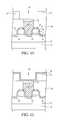
- FIG. 18shows a second embodiment of the invention, which uses a first and second oxygen sink spacers, 61 and 71 , respectively, as well as a first and second metal layers, 62 and 72 , respectively, formed before a first oxygen sink layer 64 is formed.
- Layers 62 , 71 , 72 and 64are sequentially formed in a way similar to that employed for the formation of metal layer 62 (FIG. 13) and oxygen sink layer 64 (FIGS. 14 - 15 ), described with respect to the formation of the first embodiment of the present invention. As shown in FIG.
- each of the layers 62 , 71 , 72 and 64is chemical mechanical polished (CMP) so that each of their upper surfaces end at the upper surface of the second insulating layer 25 , where a capacitor structure can be built in the manner shown and described with reference to FIGS. 16 and 17.
- CMPchemical mechanical polished
- layers 62 , 71 , 72 and 64could extend over and cover the upper surfaces of the second insulating layer 25 , as long as the conductor 81 of a fabricated overlying capacitor can connect with conductive layers 62 and 72 .
- FIG. 19illustrates yet a third embodiment of the present invention, which uses an oxygen sink layer that is not a good barrier to oxygen diffusion.
- An example of such oxygen sink materialis titanium.
- nitride layers 93 , 95 and 97 formed of silicon nitride, for example, which is a good oxygen barrier,is used in connection with titanium oxygen sink spacers 61 and 71 , and titanium layer 64 .
- the first and second oxygen sink spacers, 61 and 71formed of titanium, as well as a first and second metal layers, 62 and 72 , respectively, are formed before the titanium layer 64 is formed.
- Layers 93 , 62 , 95 , 71 , 72 , 97 and 64are sequentially formed in a way similar to that employed for the formation of metal layer 62 (FIG. 13) and oxygen sink layer 64 (FIGS. 14 - 15 ), described with respect to the formation of the first embodiment of the present invention.
- the structureis chemical mechanical polished (CMP) so that each of their upper surfaces end at the upper surface of the second insulating layer 25 , where a capacitor structure can be built.
- CMPchemical mechanical polished
- FIG. 20shows a capacitor 80 formed on the FIG. 18 structure.
- the capacitor 80includes a first ruthenium oxide conductor layer 81 , a tantalum oxide dielectric layer 82 , and a second ruthenium oxide conductor layer 83 .
- the capacitoris formed so that conductor 81 is in contact with metal conductors 62 and 72 .
- the oxygen frontwill start from the first ruthenium oxide conductor 81 , and move towards the polysilicon plug 50 .
- the oxygen frontis delayed by oxygen sink spacers 61 , 71 , and 64 and will not reach the bottom of the metal layer 62 , which connects to the barrier layer 52 , preventing therefore the formation of a barrier oxide layer, such as oxide layer 53 of FIG. 3. Further steps to create a functional memory cell containing the metal oxide-metal-polysilicon contact (FIGS. 15 - 20 ) may now be carried out to form other conductors or structures necessary for memory cell fabrication.
- the metal used for layers 62 and 72must be one of those in which the metal oxide is conductive. Suitable materials include platinum, rhodium, ruthenium, and iridium, among others.
- a typical processor based system 400which includes a memory circuit 448 , e.g. a DRAM, containing metal-polysilicon contacts according to the present invention is illustrated in FIG. 21.
- a processor systemsuch as a computer system, generally comprises a central processing unit (CPU) 444 , such as a microprocessor, a digital signal processor, or other programmable digital logic device, which communicates with an input/output (I/O) device 446 over a bus 452 .
- the memory 448communicates with the central processing unit 444 over bus 452 .
- the processor systemmay include peripheral devices such as a floppy disk drive 454 and a compact disk (CD) ROM drive 456 which also communicate with CPU 444 over the bus 452 .
- Memory 448is preferably constructed as an integrated circuit, which includes metal-polysilicon contacts formed as previously described with respect to the embodiments described in connection with FIGS. 4 to 20 .
- the memory 448may also be combined with the processor, e.g. CPU 444 , on a single integrated circuit chip. It is also possible to employ the invention in metal-polysilicon contacts within said processor.
- the exemplary embodiments described aboverefer to one or two oxygen sink spacers and oxygen sink layers, and one or two metal layers for the formation of the metal oxide-metal-polysilicon contact (FIGS. 15 - 20 ), it is to be understood that the present invention contemplates the use of a plurality of oxygen sink spacers, oxygen sink layers, and metal layers, and it is not limited by the illustrated embodiments. Accordingly, the above description and drawings are only to be considered illustrative of exemplary embodiments which achieve the features and advantages of the present invention. Modification and substitutions to specific process conditions and structures can be made without departing from the spirit and scope of the present invention. Accordingly, the invention is not to be considered as being limited by the foregoing description and drawings, but is only limited by the scope of the appended claims.
Landscapes
- Engineering & Computer Science (AREA)
- Power Engineering (AREA)
- Physics & Mathematics (AREA)
- Condensed Matter Physics & Semiconductors (AREA)
- General Physics & Mathematics (AREA)
- Manufacturing & Machinery (AREA)
- Computer Hardware Design (AREA)
- Microelectronics & Electronic Packaging (AREA)
- Semiconductor Memories (AREA)
Abstract
Description
- The present invention relates to the field of semiconductor integrated circuits and, in particular, to metal-polysilicon contacts capable of tolerating high temperature oxidizing environments.[0001]
- Semiconductor integrated circuits with high device density pose increasing difficulty to the formation of high-reliability electrical connections between metalization layers and semiconductor elements, particularly between the metal of a metallic electrode and the adjacent polysilicon of a polysilicon plug. This increased difficulty stems mainly from the tendency of metal and silicon to interdiffuse when in contact with each other, and when subjected to the high temperatures necessary during the fabrication of integrated circuits.[0002]
- To illustrate the tendency of metal-silicon interdiffusion, the formation of a metallic contact between a polysilicon plug and a metallic electrode at a specified contact area will be briefly described bellow. FIG. 1 depicts a portion of a conventional memory cell construction for a DRAM at an intermediate stage of the fabrication, in which a metal-polysilicon contact is formed according to conventional processes.[0003]
- A pair of memory cells having[0004]
respective access transistors 33 are formed within awell 13 of asubstrate 12. The wells and transistors are surrounded by afield oxide region 14 that provides isolation. N-typeactive regions 16 are provided in the doped p-type well 13 of substrate12 (for NMOS transistors) and the pair of access transistors haverespective gate stacks 30. Thegate stacks 30 include anoxide layer 18, aconductive layer 20, such as poly silicon,nitride spacers 32, and anitride cap 22.Additional stacks 31 may also be formed for use in performing self aligned contact etches to form conductive plugs for capacitor structures in the region betweenstacks - Next, a polysilicon plug[0005]50 (FIG. 1) is formed in a contact opening of a first
insulating layer 24, to directly connect to a source ordrain region 16 of the semiconductor device. The firstinsulating layer 24 could be, for example, borophosphosilicate glass (BPSG), borosilicate glass (BSG), or phosphosilicate glass (PSG). Once thepolysilicon plug 50 is formed, the whole structure, including thesubstrate 12 with the gate stacks30, the firstinsulating layer 24 and thepolysilicon plug 50, is chemically or mechanically polished to provide a planarized surface. - At this point, a second[0006]
insulating layer 25, which can be of the same material as that of the firstinsulating layer 24, is deposited over the firstinsulating layer 24 and thepolysilicon plug 50. A contact opening or via is etched over thepolysilicon plug 50 and a metal layer ormetal electrode 55 is then deposited and patterned to connect to thepolysilicon plug 50, as illustrated in FIG. 1. Thus,polysilicon plug 50 comes into contact with the metal layer orelectrode 55 at a metal-polysilicon interface51 (FIG. 1). It must be understood, however, that, as known in the art, any other conductor, such as a capacitor plate for example, may also be in contact with a polysilicon plug, and the discussion herein applies to any metal-polysilicon interface. - Since several steps during the IC fabrication require temperatures higher than 500° C., such as annealing steps, for example, silicon from the[0007]
polysilicon plug 50 migrates into the metal film of themetallic electrode 55 during these high-temperature steps. Although this silicon migration into the metal film occurs in limited regions, near or at the metal-polysilicon interface 51, since the migrated silicon has high resistivity, the contact resistance at the metal-polysilicon interface 51 is greatly increased. - Barrier layers have been introduced to solve the silicon diffusion problem at the metal-polysilicon contact, such as interface[0008]51 (FIG. 1). A
barrier layer 52 is illustrated in FIG. 2 (which shows only a middle portion of the structure of FIG. 1). Conventionally, the barrier layer is a refractory metal compound such as refractory metal nitrides (for example TiN or HfN), refractory metal carbides (for example TiC or WC), or refractory metal borides (for example TiB or MoB). Barrier layers suppress the diffusion of the silicon and metal atoms at the polysilicon-metal interface, while offering a low resistivity and low contact resistance between the silicon and the barrier layer, and between the metal and the barrier layer. However, there is a problem with such barrier layers in that, in an O2high temperature environment, they oxidize and disconnect the metal layer from the polysilicon plug. The oxide of the barrier layer may be formed either between the metal and the barrier layer, or between the polysilicon and the barrier layer. The latter situation is illustrated in FIG. 3, which showsmetal oxide layer 53 formed betweenbarrier layer 52 andpolysilicon plug 50. In either case, the oxide of the barrier layer affects the conductive properties of the metal contact by increasing the electric resistance in the electrical connection region. - In an effort to reduce the oxidation problems posed by barrier layers subjected to oxidizing environments, different techniques have been introduced into the IC fabrication. One of them is manipulating and controlling the deposition parameters of the barrier materials. For example, U.S. Pat. No. 4,976,839 discloses that the presence of an oxide at grain boundaries within a titanium nitride (TiN) barrier layer improves the ability of the barrier layer to prevent the diffusion of silicon and aluminum. The reference further discloses a method for forming a barrier layer having large grain sizes by increasing the substrate temperature during sputtering, so that the formation of the oxide at the grain boundaries may be accomplished with a relatively large amount of oxygen, but without degradation in the film conductivity.[0009]
- Similarly, to further improve the characteristics of the barrier layers, certain metals, for which both the oxidized species (MeO) as well as the unoxidized species (Me) are electrically conducting, have been recently used as barrier layers between metal and polysilicon. Examples of these metals are ruthenium (Ru), platinum (Pt), or iridium (Ir), among others. Since these barrier layers are conductive in both the metal and the oxide forms, this approach is useful in that both the oxide and the metal forms slow down the oxidation front in an O[0010]2high temperature environment. However, this technique has a drawback in that there will still be some areas where the metal does not oxidize and, thus, the barrier layer would consist of portions of pure metal species and portions of metal oxide.
- Accordingly, there is a need for an improved method for slowing down the oxidation front in barrier layers used in contacts between metal and polysilicon so that there is no oxidation at the polysilicon-metal interface. There is also a need for metal-polysilicon contacts that inhibit the diffusion of silicon and metal atoms at a contact interface and prevent the formation of oxides under high temperature O[0011]2environment, as well as a method of forming such metal-polysilicon contacts.
- The present invention provides a method for forming a metal-polysilicon contact that would be capable of tolerating an O[0012]2environment up to several hundred degrees Celsius for several hours. To prevent a metal oxide front, which is formed during a high temperature O2treatment from reaching the metal film at the metal-polysilicon interface, the metal film is surrounded by a plurality of oxygen sinks. These oxygen sinks are oxidized before the metal film at the bottom of the plug is oxidized. Accordingly, the conductive connection between the polysilicon and any device built on top of the barrier layer is preserved.
- Additional advantages of the present invention will be more apparent from the detailed description and accompanying drawings, which illustrate preferred embodiments of the invention.[0013]
- FIG. 1 is a schematic cross-sectional view of a portion of a conventional memory DRAM device illustrating a metal-polysilicon contact formed in accordance with a method of the prior art.[0014]
- FIG. 2 is a schematic cross-sectional view of the FIG. 1 device illustrating use of a barrier layer in a metal-polysilicon contact formed in accordance with the prior art.[0015]
- FIG. 3 is a schematic cross-sectional view of the FIG. 2 device depicting the formation of an oxide layer between a polysilicon plug and a barrier layer.[0016]
- FIG. 4 is a schematic cross-sectional view of a portion of a memory DRAM device, in which a metal-polysilicon contact according to a first embodiment and method of the present invention will be formed.[0017]
- FIG. 5 is a schematic cross sectional view of the FIG. 4 device at a stage of processing subsequent to that shown in FIG. 4.[0018]
- FIG. 6 is a schematic cross sectional view of the FIG. 5 device at a stage of processing subsequent to that shown in FIG. 5.[0019]
- FIG. 7 is a schematic cross sectional view of the FIG. 6 device at a stage of processing subsequent to that shown in FIG. 6.[0020]
- FIG. 8 is a schematic cross sectional view of the FIG. 7 device at a stage of processing subsequent to that shown in FIG. 7.[0021]
- FIG. 9 is a schematic cross sectional view of the FIG. 8 device at a stage of processing subsequent to that shown in FIG. 8.[0022]
- FIG. 10 is a schematic cross sectional view of the FIG. 9 device at a stage of processing subsequent to that shown in FIG. 9.[0023]
- FIG. 11 is a schematic cross sectional view of the FIG. 10 device at a stage of processing subsequent to that shown in FIG. 10.[0024]
- FIG. 12 is a schematic cross sectional view of the FIG. 11 device at a stage of processing subsequent to that shown in FIG[0025]11.
- FIG. 13 is a schematic cross sectional view of the FIG. 12 device at a stage of processing subsequent to that shown in FIG. 12.[0026]
- FIG. 14 is a schematic cross sectional view of the FIG. 13 device at a stage of processing subsequent to that shown in FIG. 13.[0027]
- FIG. 15 is a schematic cross sectional view of the FIG. 14 device at a stage of processing subsequent to that shown in FIG. 14.[0028]
- FIG. 16 is a schematic cross sectional view of the FIG. 15 device at a stage of processing subsequent to that shown in FIG. 15, and depicting a capacitor formed over the metal-polysilicon contact.[0029]
- FIG. 17 is a schematic cross sectional view of the FIG. 16 device at a stage of processing subsequent to that shown in FIG. 16.[0030]
- FIG. 18 is a schematic cross sectional view of the FIG. 14 device at a stage of processing subsequent to that shown in FIG. 14, and in accordance with a second embodiment of the present invention.[0031]
- FIG. 19 is a schematic cross sectional view of the FIG. 14 device at a stage of processing subsequent to that shown in FIG. 14, and in accordance with a third embodiment of the present invention.[0032]
- FIG. 20 is a schematic cross sectional view of the FIG. 18 device at a stage of processing subsequent to that shown in FIG. 18, and depicting a capacitor formed over the metal-polysilicon contact.[0033]
- FIG. 21 is an illustration of a computer system having a memory device employing the present invention.[0034]
- In the following detailed description, reference is made to various specific embodiments in which the invention may be practiced. These embodiments are described with sufficient detail to enable those skilled in the art to practice the invention, and it is to be understood that other embodiments may be employed, and that structural, logical, and electrical changes may be made without departing from the spirit or scope of the present invention.[0035]
- The term “substrate” used in the following description may include any semiconductor-based structure that has an exposed silicon surface. Structure must be understood to include silicon-on insulator (SOI), silicon-on sapphire (SOS), doped and undoped semiconductors, epitaxial layers of silicon supported by a base semiconductor foundation, and other semiconductor structures. The semiconductor need not be silicon-based. The semiconductor could be silicon-germanium, germanium, or gallium arsenide. When reference is made to substrate in the following description, previous process steps may have been utilized to form regions or junctions in or on the base semiconductor or foundation.[0036]
- The present invention provides a method for forming a metal oxide-metal-polysilicon contact capable of tolerating on oxygen environment up to several hundred degrees and for several hours. The invention provides one or more oxygen sink layers, which are oxidized before the metal film is oxidized at the metal-polysilicon interface. The oxygen sink layers slow down the oxidation front of the metal film, so it does not reach the metal-polysilicon interface.[0037]
- FIG. 4 depicts a conventional memory cell construction for a DRAM at an intermediate stage of the fabrication, in which a pair of memory cells having respective access transistors are formed on a[0038]
substrate 12. The FIG. 4 structure includes thesubstrate 12 having a well13, which is typically doped to a predetermined conductivity, e.g. p-type or n-type depending on whether NMOS or PMOS transistors will be formed therein. The structure further includesfield oxide regions 14, conventional dopedactive areas 16 for use as source/drain regions, and a pair of gate stacks30, all formed according to well-known semiconductor processing techniques. The gate stacks30 include anoxide layer 18, aconductive layer 20, such as polysilicon,nitride spacers 32 and anitride cap 22. - Above the[0039]
gate oxide region 18,tie polysilicon gates 20, and theprotective nitride regions layer 24 could be, for example, borophosphosilicate glass (BPSG), borosilicate glass (BSG), or phosphosilicate glass (PSG). - Reference is now made to FIG. 5, which for simplicity illustrates only a lateral portion, for example a right side portion, of FIG. 4. This is a region where a contact plug and an overlying capacitor structure will be formed. To create a contact opening[0040]40 (FIG. 6) into
semiconductor substrate 12 through the first insulatinglayer 24, a photoresist material26 (FIG. 5) is deposited and patterned using conventional photolithography steps. After patterning, an initial opening27 (FIG. 5) is present in photoresist layer26 for subsequent oxide etching. The structure of FIG. 5 is then etched, to form acontact opening 40 through first insulatinglayer 24 and the photoresist layer is removed as shown in FIG. 6. Thecontact opening 40 is etched so thatcontact opening 40 extends to a source/drain region 16 provided in well13 ofsubstrate 12. - Next,[0041]
contact opening 40 is filled with a conductive material, such as doped polysilicon, that is planarized down to or near the planar surface of the first insulatinglayer 24, to form a polysilicon plug orfiller 50, as illustrated in FIG. 7. Thepolysilicon plug 50 is then anisotropically etched until its top surface is recessed below the planar surface of the first insulatinglayer 24, so that a barrier layer52 (FIG. 8) can be deposited and planarized, as shown in FIG. 8. Thebarrier layer 52, preferably of titanium (Ti), is formed on thepolysilicon plug 50 by CVD, PVD, sputtering or evaporation, to a thickness of about 60 to about 200 Angstroms. Thetitanium barrier layer 52 will form titanium silicide (TiSi2) during a later high temperature anneal. - FIG. 9 illustrates the deposition of a second insulating[0042]
layer 25, which could be, for example, a silicon oxide, borophosphosilicate glass (BPSG), borosilicate glass (BSG), phosphosilicate glass (PSG), or tetraethylorthosilicate (TEOS). The second insulatinglayer 25 is deposited over thebarrier layer 52 and the first insulatinglayer 24. Again, using the same fabrication technique as the one used for the formation of contact opening40 (FIG. 6) through the first insulatinglayer 24, a contact opening41 (FIG. 10) is formed through the second insulatinglayer 25. - Subsequent to the formation of contact opening[0043]41 of FIG. 10, a material acting as an oxygen sink is deposited by using plasma, reactive sputtering or a conventional chemical vapor deposition to form a first
oxygen sink layer 60, as shown in FIG. 11, to a thickness of about100 Angstroms. Preferred materials for the firstoxygen sink layer 60 are polysilicon, aluminum nitride, titanium, titanium nitride, silicon nitride, or tantalum, among others. A characteristic of the sink material is that it oxidizes in a high temperature O2environment. Although some of the metals employed as oxygen sink oxidize and become therefore nonconductive, this fact raises no problems because, in the embodiments described below, these metals are used strictly as oxygen sinks and not as barrier layers. After deposition of theoxygen sink layer 60, a spacer etch is employed to remove portions of the firstoxygen sink layer 60 inside thecontact opening 41 and on the planar surface of the second insulatinglayer 25, leaving only spacers61 formed of oxygen sink material on the side walls ofcontact opening 41, as illustrated in FIG. 12. The etch stops at the upper surface of thebarrier layer 52, without damaging, or etching into, the upper surface of thebarrier layer 52. - Next, referring to FIG. 13, a[0044]
layer 62 of conductive metal is formed inside thecontact opening 41, over the upper surface of thebarrier layer 52, over thespacers 61 and over the upper surface of insulatinglayer 25. Although FIG. 13 illustrates themetal layer 62 as formed over the upper surface of the second insulatinglayer 25, it is to be understood thatmetal layer 62 does not have to cover the second insulatinglayer 25. Depending on the type of devices that would be further built to complete the formation of a DRAM memory cell, themetal layer 62 may or may not extend over the second insulatinglayer 25, as long as it is formed inside of thecontact opening 41. - Preferred materials for the[0045]
conductive material layer 62 are metal conductors which, when oxidized, are still conductive, such as platinum (Pt), ruthenium (Ru), iridium (Ir), rhodium (Rh) and their respective oxides, or any other metal capable of forming a metal-barrier layer-polysilicon contact on top of the polysilicon plug orfiller 50.Metal layer 62 could be formed by any conventional method, such as deposition or sputtering, to a thickness of approximately 100 to 300 Angstroms. - A second[0046]
oxygen sink layer 64 is next formed over the metal ormetal oxide layer 62. This is illustrated in FIG. 14. The material for this secondoxygen sink layer 64 may be, for example, a material which oxidizes at high temperature O2environment, such as polysilicon, aluminum nitride, titanium nitride, silicon nitride, or tantalum. The secondoxygen sink layer 64 is then chemically metal polished (CMP) to formoxygen sink layer 64 of FIG. 15, on top of which another device could now be built. - For example, as shown in FIG. 16, a[0047]
capacitor 80 formed of a first ruthenium oxide conductor (RuOx)layer 81, a tantalum oxide dielectric (TaOx)layer 82, and a second ruthenium oxide conductor (RuOx)layer 83 can be formed in an opening created in a third insulatinglayer 27 provided over the second insulatinglayer 25, at a position on top of the upper surface of theoxygen sink layer 64. TheRuOx layer 81 is fabricated to be in contact with metal (or metal oxide)layer 62. As known in the art, during the fabrication process of thecapacitor 80, the firstruthenium oxide conductor 81 requires an N2/O2anneal, in an oxygen environment at high temperatures. Thus, during the anneal step, an oxygen front will move through the firstruthenium oxide conductor 81, and move towards theoxygen sink layer 64, themetal layer 62 and thebarrier layer 52, towards thepolysilicon plug 50, as shown in FIG. 17. The oxygen front will be delayed by the oxygen sink layers64 and61, but will nevertheless start oxidizing themetal layer 62 from the top of the upper surface of the second insulatinglayer 25. - The oxygen sink layers[0048]64 and61 slow the movement of the oxygen front so that it never reaches
barrier layer 52 during the N2/O2anneal. This is shown in FIG. 17. The upper portion of themetal layer 62 may oxidize during the anneal process to form a conductivemetal oxide layer 62a,but the remaining portion of themetal layer 62 is not oxidized during the anneal process as is shown byunoxidized metal layer 62b.Thus, an effective conductive path fromcapacitor conductor 81 toconductive plug 50, throughmetal oxide layer 62a,metal layer 62b,andbarrier layer 52, is provided. - As a general proposition, it should be clear that the thicker the[0049]
oxygen sink layer 64, the slower the advancement of the oxygen front towards thebarrier layer 52 and thepolysilicon plug 50. Similarly, the greater the number of oxygen sink layers, the slower the advancement of the oxygen front towards thebarrier layer 52. Of course, as well-known in the art, the advancement of the oxygen front toward thepolysilicon plug 50 is also slowed down by employing a high aspect ratio contact, that is, a contact with a small cross section A (FIG. 17) but a large height L (FIG. 17) of thespacers 61 formed of oxygen sink material. A high aspect ratio is, for example, an aspect ratio of 25. Thus, ideally, the oxygen front is delayed by employing a multi-layer oxygen sink in a high aspect ratio metal-polysilicon contact. - FIG. 18 shows a second embodiment of the invention, which uses a first and second oxygen sink spacers,[0050]61 and71, respectively, as well as a first and second metal layers,62 and72, respectively, formed before a first
oxygen sink layer 64 is formed.Layers layers layer 25, where a capacitor structure can be built in the manner shown and described with reference to FIGS. 16 and 17. Of course, as explained above, layers62,71,72 and64 could extend over and cover the upper surfaces of the second insulatinglayer 25, as long as theconductor 81 of a fabricated overlying capacitor can connect withconductive layers - FIG. 19 illustrates yet a third embodiment of the present invention, which uses an oxygen sink layer that is not a good barrier to oxygen diffusion. An example of such oxygen sink material is titanium. In this embodiment, nitride layers[0051]93,95 and97 formed of silicon nitride, for example, which is a good oxygen barrier, is used in connection with titanium
oxygen sink spacers titanium layer 64. As explained above, the first and second oxygen sink spacers,61 and71, formed of titanium, as well as a first and second metal layers,62 and72, respectively, are formed before thetitanium layer 64 is formed.Layers layers layer 25, where a capacitor structure can be built. - FIG. 20 shows a[0052]
capacitor 80 formed on the FIG. 18 structure. Thecapacitor 80 includes a first rutheniumoxide conductor layer 81, a tantalumoxide dielectric layer 82, and a second rutheniumoxide conductor layer 83. The capacitor is formed so thatconductor 81 is in contact withmetal conductors ruthenium oxide conductor 81, the oxygen front will start from the firstruthenium oxide conductor 81, and move towards thepolysilicon plug 50. The oxygen front is delayed byoxygen sink spacers metal layer 62, which connects to thebarrier layer 52, preventing therefore the formation of a barrier oxide layer, such asoxide layer 53 of FIG. 3. Further steps to create a functional memory cell containing the metal oxide-metal-polysilicon contact (FIGS.15-20) may now be carried out to form other conductors or structures necessary for memory cell fabrication. - It should be noted again that the metal used for[0053]
layers - A typical processor based[0054]
system 400 which includes amemory circuit 448, e.g. a DRAM, containing metal-polysilicon contacts according to the present invention is illustrated in FIG. 21. A processor system, such as a computer system, generally comprises a central processing unit (CPU)444, such as a microprocessor, a digital signal processor, or other programmable digital logic device, which communicates with an input/output (I/O)device 446 over abus 452. Thememory 448 communicates with thecentral processing unit 444 overbus 452. - In the case of a computer system, the processor system may include peripheral devices such as a[0055]
floppy disk drive 454 and a compact disk (CD)ROM drive 456 which also communicate withCPU 444 over thebus 452.Memory 448 is preferably constructed as an integrated circuit, which includes metal-polysilicon contacts formed as previously described with respect to the embodiments described in connection with FIGS.4 to20. Thememory 448 may also be combined with the processor,e.g. CPU 444, on a single integrated circuit chip. It is also possible to employ the invention in metal-polysilicon contacts within said processor. - Although the exemplary embodiments described above refer to one or two oxygen sink spacers and oxygen sink layers, and one or two metal layers for the formation of the metal oxide-metal-polysilicon contact (FIGS.[0056]15-20), it is to be understood that the present invention contemplates the use of a plurality of oxygen sink spacers, oxygen sink layers, and metal layers, and it is not limited by the illustrated embodiments. Accordingly, the above description and drawings are only to be considered illustrative of exemplary embodiments which achieve the features and advantages of the present invention. Modification and substitutions to specific process conditions and structures can be made without departing from the spirit and scope of the present invention. Accordingly, the invention is not to be considered as being limited by the foregoing description and drawings, but is only limited by the scope of the appended claims.
Claims (109)
Priority Applications (2)
| Application Number | Priority Date | Filing Date | Title |
|---|---|---|---|
| US09/930,268US6472322B2 (en) | 2000-08-29 | 2001-08-16 | Method of forming a metal to polysilicon contact in oxygen environment |
| US10/274,156US6787465B2 (en) | 2000-08-29 | 2002-10-21 | Method of forming a metal to polysilicon contact in oxygen environment |
Applications Claiming Priority (2)
| Application Number | Priority Date | Filing Date | Title |
|---|---|---|---|
| US09/650,071US6583460B1 (en) | 2000-08-29 | 2000-08-29 | Method of forming a metal to polysilicon contact in oxygen environment |
| US09/930,268US6472322B2 (en) | 2000-08-29 | 2001-08-16 | Method of forming a metal to polysilicon contact in oxygen environment |
Related Parent Applications (1)
| Application Number | Title | Priority Date | Filing Date |
|---|---|---|---|
| US09/650,071DivisionUS6583460B1 (en) | 2000-08-29 | 2000-08-29 | Method of forming a metal to polysilicon contact in oxygen environment |
Related Child Applications (1)
| Application Number | Title | Priority Date | Filing Date |
|---|---|---|---|
| US10/274,156ContinuationUS6787465B2 (en) | 2000-08-29 | 2002-10-21 | Method of forming a metal to polysilicon contact in oxygen environment |
Publications (2)
| Publication Number | Publication Date |
|---|---|
| US20020025665A1true US20020025665A1 (en) | 2002-02-28 |
| US6472322B2 US6472322B2 (en) | 2002-10-29 |
Family
ID=24607323
Family Applications (5)
| Application Number | Title | Priority Date | Filing Date |
|---|---|---|---|
| US09/650,071Expired - LifetimeUS6583460B1 (en) | 2000-08-29 | 2000-08-29 | Method of forming a metal to polysilicon contact in oxygen environment |
| US09/930,268Expired - LifetimeUS6472322B2 (en) | 2000-08-29 | 2001-08-16 | Method of forming a metal to polysilicon contact in oxygen environment |
| US10/118,947Expired - LifetimeUS6677632B2 (en) | 2000-08-29 | 2002-04-10 | Method of forming a metal to polysilicon contact in oxygen environment |
| US10/274,156Expired - LifetimeUS6787465B2 (en) | 2000-08-29 | 2002-10-21 | Method of forming a metal to polysilicon contact in oxygen environment |
| US10/734,260Expired - LifetimeUS7262473B2 (en) | 2000-08-29 | 2003-12-15 | Metal to polysilicon contact in oxygen environment |
Family Applications Before (1)
| Application Number | Title | Priority Date | Filing Date |
|---|---|---|---|
| US09/650,071Expired - LifetimeUS6583460B1 (en) | 2000-08-29 | 2000-08-29 | Method of forming a metal to polysilicon contact in oxygen environment |
Family Applications After (3)
| Application Number | Title | Priority Date | Filing Date |
|---|---|---|---|
| US10/118,947Expired - LifetimeUS6677632B2 (en) | 2000-08-29 | 2002-04-10 | Method of forming a metal to polysilicon contact in oxygen environment |
| US10/274,156Expired - LifetimeUS6787465B2 (en) | 2000-08-29 | 2002-10-21 | Method of forming a metal to polysilicon contact in oxygen environment |
| US10/734,260Expired - LifetimeUS7262473B2 (en) | 2000-08-29 | 2003-12-15 | Metal to polysilicon contact in oxygen environment |
Country Status (1)
| Country | Link |
|---|---|
| US (5) | US6583460B1 (en) |
Cited By (21)
| Publication number | Priority date | Publication date | Assignee | Title |
|---|---|---|---|---|
| US20040140494A1 (en)* | 2000-08-31 | 2004-07-22 | Micron Technology, Inc. | Contact structure |
| CN107026134A (en)* | 2015-12-21 | 2017-08-08 | 台湾积体电路制造股份有限公司 | Semiconductor structure and its manufacture method |
| KR20180034671A (en)* | 2015-08-25 | 2018-04-04 | 인벤사스 본딩 테크놀로지스 인코포레이티드 | Conductive Barrier Direct Hybrid Junction |
| US10840205B2 (en) | 2017-09-24 | 2020-11-17 | Invensas Bonding Technologies, Inc. | Chemical mechanical polishing for hybrid bonding |
| US11011418B2 (en) | 2005-08-11 | 2021-05-18 | Invensas Bonding Technologies, Inc. | 3D IC method and device |
| US11011494B2 (en) | 2018-08-31 | 2021-05-18 | Invensas Bonding Technologies, Inc. | Layer structures for making direct metal-to-metal bonds at low temperatures in microelectronics |
| US11158573B2 (en) | 2018-10-22 | 2021-10-26 | Invensas Bonding Technologies, Inc. | Interconnect structures |
| US11244920B2 (en) | 2018-12-18 | 2022-02-08 | Invensas Bonding Technologies, Inc. | Method and structures for low temperature device bonding |
| US11393779B2 (en) | 2018-06-13 | 2022-07-19 | Invensas Bonding Technologies, Inc. | Large metal pads over TSV |
| US11515279B2 (en) | 2018-04-11 | 2022-11-29 | Adeia Semiconductor Bonding Technologies Inc. | Low temperature bonded structures |
| US11710718B2 (en) | 2015-07-10 | 2023-07-25 | Adeia Semiconductor Technologies Llc | Structures and methods for low temperature bonding using nanoparticles |
| US11728313B2 (en) | 2018-06-13 | 2023-08-15 | Adeia Semiconductor Bonding Technologies Inc. | Offset pads over TSV |
| US11735523B2 (en) | 2020-05-19 | 2023-08-22 | Adeia Semiconductor Bonding Technologies Inc. | Laterally unconfined structure |
| US11804377B2 (en) | 2018-04-05 | 2023-10-31 | Adeia Semiconductor Bonding Technologies, Inc. | Method for preparing a surface for direct-bonding |
| US11894326B2 (en) | 2017-03-17 | 2024-02-06 | Adeia Semiconductor Bonding Technologies Inc. | Multi-metal contact structure |
| US11908739B2 (en) | 2017-06-05 | 2024-02-20 | Adeia Semiconductor Technologies Llc | Flat metal features for microelectronics applications |
| US11929347B2 (en) | 2020-10-20 | 2024-03-12 | Adeia Semiconductor Technologies Llc | Mixed exposure for large die |
| US11973056B2 (en) | 2016-10-27 | 2024-04-30 | Adeia Semiconductor Technologies Llc | Methods for low temperature bonding using nanoparticles |
| US12100676B2 (en) | 2018-04-11 | 2024-09-24 | Adeia Semiconductor Bonding Technologies Inc. | Low temperature bonded structures |
| US12211809B2 (en) | 2020-12-30 | 2025-01-28 | Adeia Semiconductor Bonding Technologies Inc. | Structure with conductive feature and method of forming same |
| US12381128B2 (en) | 2020-12-28 | 2025-08-05 | Adeia Semiconductor Bonding Technologies Inc. | Structures with through-substrate vias and methods for forming the same |
Families Citing this family (17)
| Publication number | Priority date | Publication date | Assignee | Title |
|---|---|---|---|---|
| US6583460B1 (en)* | 2000-08-29 | 2003-06-24 | Micron Technology, Inc. | Method of forming a metal to polysilicon contact in oxygen environment |
| US6713373B1 (en)* | 2002-02-05 | 2004-03-30 | Novellus Systems, Inc. | Method for obtaining adhesion for device manufacture |
| US6908807B2 (en)* | 2002-03-26 | 2005-06-21 | Micron Technology, Inc. | Methods of forming semiconductor constructions |
| US6815753B2 (en)* | 2002-08-29 | 2004-11-09 | Micron Technology, Inc. | Semiconductor capacitor structure and method to form same |
| KR100504693B1 (en)* | 2003-02-10 | 2005-08-03 | 삼성전자주식회사 | Ferroelectric memory device and method for fabricating the same |
| KR100558008B1 (en)* | 2003-12-29 | 2006-03-06 | 삼성전자주식회사 | Wiring Method of Semiconductor Devices |
| DE102004004864B4 (en)* | 2004-01-30 | 2008-09-11 | Qimonda Ag | Method for producing a gate structure and gate structure for a transistor |
| JP4560814B2 (en)* | 2004-06-17 | 2010-10-13 | エルピーダメモリ株式会社 | Manufacturing method of semiconductor device |
| US20050287793A1 (en)* | 2004-06-29 | 2005-12-29 | Micron Technology, Inc. | Diffusion barrier process for routing polysilicon contacts to a metallization layer |
| US7037774B1 (en)* | 2004-10-21 | 2006-05-02 | Integrated Device Technology, Inc. | Self-aligned contact structure and process for forming self-aligned contact structure |
| US7364997B2 (en) | 2005-07-07 | 2008-04-29 | Micron Technology, Inc. | Methods of forming integrated circuitry and methods of forming local interconnects |
| CN101399266B (en)* | 2007-09-29 | 2010-08-25 | 中芯国际集成电路制造(上海)有限公司 | Modified capacitor and method for manufacturing same |
| KR101099958B1 (en)* | 2007-11-20 | 2011-12-28 | 주식회사 하이닉스반도체 | Metal wiring formation method of semiconductor device |
| FR2960700B1 (en)* | 2010-06-01 | 2012-05-18 | Commissariat Energie Atomique | LITHOGRAPHY METHOD FOR REALIZING VIAS-CONNECTED CONDUCTOR NETWORKS |
| US10777562B1 (en) | 2019-03-14 | 2020-09-15 | Micron Technology, Inc. | Integrated circuity, DRAM circuitry, methods used in forming integrated circuitry, and methods used in forming DRAM circuitry |
| KR20240003827A (en)* | 2022-07-04 | 2024-01-11 | 한양대학교 산학협력단 | Capacitor of dram device and manufacturing method therefor |
| KR102673262B1 (en)* | 2023-03-22 | 2024-06-10 | 한양대학교 산학협력단 | Capacitor of dram and manufacturing method therefor |
Family Cites Families (22)
| Publication number | Priority date | Publication date | Assignee | Title |
|---|---|---|---|---|
| US4394406A (en)* | 1980-06-30 | 1983-07-19 | International Business Machines Corp. | Double polysilicon contact structure and process |
| US4960732A (en)* | 1987-02-19 | 1990-10-02 | Advanced Micro Devices, Inc. | Contact plug and interconnect employing a barrier lining and a backfilled conductor material |
| JPH0666287B2 (en) | 1988-07-25 | 1994-08-24 | 富士通株式会社 | Method for manufacturing semiconductor device |
| US6081034A (en)* | 1992-06-12 | 2000-06-27 | Micron Technology, Inc. | Low-resistance contact to silicon having a titanium silicide interface and an amorphous titanium carbonitride barrier layer |
| US5354705A (en) | 1993-09-15 | 1994-10-11 | Micron Semiconductor, Inc. | Technique to fabricate a container structure with rough inner and outer surfaces |
| US5773363A (en)* | 1994-11-08 | 1998-06-30 | Micron Technology, Inc. | Semiconductor processing method of making electrical contact to a node |
| KR100193100B1 (en) | 1995-02-02 | 1999-06-15 | 모리시다 요이치 | Semiconductor device and manufacturing method |
| US5756396A (en) | 1996-05-06 | 1998-05-26 | Taiwan Semiconductor Manufacturing Company Ltd | Method of making a multi-layer wiring structure having conductive sidewall etch stoppers and a stacked plug interconnect |
| KR100239418B1 (en)* | 1996-12-03 | 2000-01-15 | 김영환 | Capacitor of Semiconductor Device and Manufacturing Method Thereof |
| US5770520A (en) | 1996-12-05 | 1998-06-23 | Lsi Logic Corporation | Method of making a barrier layer for via or contact opening of integrated circuit structure |
| JPH10333237A (en)* | 1997-03-31 | 1998-12-18 | Nikon Corp | Camera magnetic reader |
| JP2001504282A (en)* | 1997-06-09 | 2001-03-27 | テルコーディア テクノロジーズ インコーポレイテッド | Annealing of crystalline perovskite ferroelectric cells and cells exhibiting improved barrier properties |
| US6277728B1 (en)* | 1997-06-13 | 2001-08-21 | Micron Technology, Inc. | Multilevel interconnect structure with low-k dielectric and method of fabricating the structure |
| US6373088B2 (en)* | 1997-06-16 | 2002-04-16 | Texas Instruments Incorporated | Edge stress reduction by noncoincident layers |
| JP3523093B2 (en)* | 1997-11-28 | 2004-04-26 | 株式会社東芝 | Semiconductor device and manufacturing method thereof |
| EP0926741A3 (en) | 1997-12-23 | 1999-11-03 | Texas Instruments Incorporated | Gate structure and method of forming same |
| KR100290895B1 (en)* | 1998-06-30 | 2001-07-12 | 김영환 | Capacitor structure of semiconductor device and manufacturing method thereof |
| US5998847A (en)* | 1998-08-11 | 1999-12-07 | International Business Machines Corporation | Low voltage active body semiconductor device |
| JP2000183311A (en)* | 1998-12-17 | 2000-06-30 | Nec Corp | Semiconductor device and manufacturing method thereof |
| US6346467B1 (en)* | 1999-09-02 | 2002-02-12 | Advanced Micro Devices, Inc. | Method of making tungsten gate MOS transistor and memory cell by encapsulating |
| TW432689B (en)* | 1999-10-18 | 2001-05-01 | Taiwan Semiconductor Mfg | Fabricating method of stacked capacitor |
| US6583460B1 (en)* | 2000-08-29 | 2003-06-24 | Micron Technology, Inc. | Method of forming a metal to polysilicon contact in oxygen environment |
- 2000
- 2000-08-29USUS09/650,071patent/US6583460B1/ennot_activeExpired - Lifetime
- 2001
- 2001-08-16USUS09/930,268patent/US6472322B2/ennot_activeExpired - Lifetime
- 2002
- 2002-04-10USUS10/118,947patent/US6677632B2/ennot_activeExpired - Lifetime
- 2002-10-21USUS10/274,156patent/US6787465B2/ennot_activeExpired - Lifetime
- 2003
- 2003-12-15USUS10/734,260patent/US7262473B2/ennot_activeExpired - Lifetime
Cited By (51)
| Publication number | Priority date | Publication date | Assignee | Title |
|---|---|---|---|---|
| US20040140494A1 (en)* | 2000-08-31 | 2004-07-22 | Micron Technology, Inc. | Contact structure |
| US6787833B1 (en)* | 2000-08-31 | 2004-09-07 | Micron Technology, Inc. | Integrated circuit having a barrier structure |
| US20050287794A1 (en)* | 2000-08-31 | 2005-12-29 | Micron Technology, Inc. | Contact structure |
| US7071055B2 (en) | 2000-08-31 | 2006-07-04 | Micron Technology, Inc. | Method of forming a contact structure including a vertical barrier structure and two barrier layers |
| US20060220087A1 (en)* | 2000-08-31 | 2006-10-05 | Micron Technology, Inc. | Method of forming a contact structure including a vertical barrier structure and two barrier layers |
| US7569453B2 (en) | 2000-08-31 | 2009-08-04 | Micron Technology, Inc. | Contact structure |
| US11289372B2 (en) | 2005-08-11 | 2022-03-29 | Invensas Bonding Technologies, Inc. | 3D IC method and device |
| US11011418B2 (en) | 2005-08-11 | 2021-05-18 | Invensas Bonding Technologies, Inc. | 3D IC method and device |
| US11515202B2 (en) | 2005-08-11 | 2022-11-29 | Adeia Semiconductor Bonding Technologies Inc. | 3D IC method and device |
| US11710718B2 (en) | 2015-07-10 | 2023-07-25 | Adeia Semiconductor Technologies Llc | Structures and methods for low temperature bonding using nanoparticles |
| KR102408487B1 (en) | 2015-08-25 | 2022-06-13 | 인벤사스 본딩 테크놀로지스 인코포레이티드 | Conductive barrier direct hybrid junction |
| KR20180034671A (en)* | 2015-08-25 | 2018-04-04 | 인벤사스 본딩 테크놀로지스 인코포레이티드 | Conductive Barrier Direct Hybrid Junction |
| US12381168B2 (en) | 2015-08-25 | 2025-08-05 | Adeia Semiconductor Bonding Technologies Inc. | Conductive barrier direct hybrid bonding |
| US9953941B2 (en)* | 2015-08-25 | 2018-04-24 | Invensas Bonding Technologies, Inc. | Conductive barrier direct hybrid bonding |
| US10262963B2 (en) | 2015-08-25 | 2019-04-16 | Invensas Bonding Technologies, Inc. | Conductive barrier direct hybrid bonding |
| US11264345B2 (en) | 2015-08-25 | 2022-03-01 | Invensas Bonding Technologies, Inc. | Conductive barrier direct hybrid bonding |
| KR102659849B1 (en) | 2015-08-25 | 2024-04-22 | 아데이아 세미컨덕터 본딩 테크놀로지스 인코포레이티드 | Conductive barrier direct hybrid bonding |
| US11830838B2 (en) | 2015-08-25 | 2023-11-28 | Adeia Semiconductor Bonding Technologies Inc. | Conductive barrier direct hybrid bonding |
| KR20220083859A (en)* | 2015-08-25 | 2022-06-20 | 인벤사스 본딩 테크놀로지스 인코포레이티드 | Conductive barrier direct hybrid bonding |
| CN107026134A (en)* | 2015-12-21 | 2017-08-08 | 台湾积体电路制造股份有限公司 | Semiconductor structure and its manufacture method |
| US11973056B2 (en) | 2016-10-27 | 2024-04-30 | Adeia Semiconductor Technologies Llc | Methods for low temperature bonding using nanoparticles |
| US12027487B2 (en) | 2016-10-27 | 2024-07-02 | Adeia Semiconductor Technologies Llc | Structures for low temperature bonding using nanoparticles |
| US11894326B2 (en) | 2017-03-17 | 2024-02-06 | Adeia Semiconductor Bonding Technologies Inc. | Multi-metal contact structure |
| US11908739B2 (en) | 2017-06-05 | 2024-02-20 | Adeia Semiconductor Technologies Llc | Flat metal features for microelectronics applications |
| US10840205B2 (en) | 2017-09-24 | 2020-11-17 | Invensas Bonding Technologies, Inc. | Chemical mechanical polishing for hybrid bonding |
| US11552041B2 (en) | 2017-09-24 | 2023-01-10 | Adeia Semiconductor Bonding Technologies Inc. | Chemical mechanical polishing for hybrid bonding |
| US12381173B2 (en) | 2017-09-24 | 2025-08-05 | Adeia Semiconductor Bonding Technologies Inc. | Direct hybrid bonding of substrates having microelectronic components with different profiles and/or pitches at the bonding interface |
| US12341018B2 (en) | 2018-04-05 | 2025-06-24 | Adeia Semiconductor Bonding Technologies Inc. | Method for preparing a surface for direct-bonding |
| US11804377B2 (en) | 2018-04-05 | 2023-10-31 | Adeia Semiconductor Bonding Technologies, Inc. | Method for preparing a surface for direct-bonding |
| US12132020B2 (en) | 2018-04-11 | 2024-10-29 | Adeia Semiconductor Bonding Technologies Inc. | Low temperature bonded structures |
| US12046571B2 (en) | 2018-04-11 | 2024-07-23 | Adeia Semiconductor Bonding Technologies Inc. | Low temperature bonded structures |
| US12100676B2 (en) | 2018-04-11 | 2024-09-24 | Adeia Semiconductor Bonding Technologies Inc. | Low temperature bonded structures |
| US11515279B2 (en) | 2018-04-11 | 2022-11-29 | Adeia Semiconductor Bonding Technologies Inc. | Low temperature bonded structures |
| US11728313B2 (en) | 2018-06-13 | 2023-08-15 | Adeia Semiconductor Bonding Technologies Inc. | Offset pads over TSV |
| US12243851B2 (en) | 2018-06-13 | 2025-03-04 | Adeia Semiconductor Bonding Technologies Inc. | Offset pads over TSV |
| US11955445B2 (en) | 2018-06-13 | 2024-04-09 | Adeia Semiconductor Bonding Technologies Inc. | Metal pads over TSV |
| US12205926B2 (en) | 2018-06-13 | 2025-01-21 | Adeia Semiconductor Bonding Technologies Inc. | TSV as pad |
| US11393779B2 (en) | 2018-06-13 | 2022-07-19 | Invensas Bonding Technologies, Inc. | Large metal pads over TSV |
| US11749645B2 (en) | 2018-06-13 | 2023-09-05 | Adeia Semiconductor Bonding Technologies Inc. | TSV as pad |
| US12136605B2 (en) | 2018-08-31 | 2024-11-05 | Adeia Semiconductor Bonding Technologies Inc. | Layer structures for making direct metal-to-metal bonds at low temperatures in microelectronics and method for forming the same |
| US11011494B2 (en) | 2018-08-31 | 2021-05-18 | Invensas Bonding Technologies, Inc. | Layer structures for making direct metal-to-metal bonds at low temperatures in microelectronics |
| US12125784B2 (en) | 2018-10-22 | 2024-10-22 | Adeia Semiconductor Bonding Technologies Inc. | Interconnect structures |
| US11756880B2 (en) | 2018-10-22 | 2023-09-12 | Adeia Semiconductor Bonding Technologies Inc. | Interconnect structures |
| US11158573B2 (en) | 2018-10-22 | 2021-10-26 | Invensas Bonding Technologies, Inc. | Interconnect structures |
| US12154880B2 (en) | 2018-12-18 | 2024-11-26 | Adeia Semiconductor Bonding Technologies Inc. | Method and structures for low temperature device bonding |
| US11244920B2 (en) | 2018-12-18 | 2022-02-08 | Invensas Bonding Technologies, Inc. | Method and structures for low temperature device bonding |
| US11735523B2 (en) | 2020-05-19 | 2023-08-22 | Adeia Semiconductor Bonding Technologies Inc. | Laterally unconfined structure |
| US12033943B2 (en) | 2020-05-19 | 2024-07-09 | Adeia Semiconductor Bonding Technologies Inc. | Laterally unconfined structure |
| US11929347B2 (en) | 2020-10-20 | 2024-03-12 | Adeia Semiconductor Technologies Llc | Mixed exposure for large die |
| US12381128B2 (en) | 2020-12-28 | 2025-08-05 | Adeia Semiconductor Bonding Technologies Inc. | Structures with through-substrate vias and methods for forming the same |
| US12211809B2 (en) | 2020-12-30 | 2025-01-28 | Adeia Semiconductor Bonding Technologies Inc. | Structure with conductive feature and method of forming same |
Also Published As
| Publication number | Publication date |
|---|---|
| US20040127022A1 (en) | 2004-07-01 |
| US7262473B2 (en) | 2007-08-28 |
| US6583460B1 (en) | 2003-06-24 |
| US6472322B2 (en) | 2002-10-29 |
| US6677632B2 (en) | 2004-01-13 |
| US6787465B2 (en) | 2004-09-07 |
| US20020110987A1 (en) | 2002-08-15 |
| US20030057467A1 (en) | 2003-03-27 |
Similar Documents
| Publication | Publication Date | Title |
|---|---|---|
| US6583460B1 (en) | Method of forming a metal to polysilicon contact in oxygen environment | |
| US6603203B2 (en) | Semiconductor device having capacitive element structure and multilevel interconnection structure and method of fabricating the same | |
| US6369430B1 (en) | Method of preventing two neighboring contacts from a short-circuit caused by a void between them and device having the same | |
| KR100491458B1 (en) | Semiconductor device | |
| US5057447A (en) | Silicide/metal floating gate process | |
| US7405112B2 (en) | Low contact resistance CMOS circuits and methods for their fabrication | |
| KR20000053397A (en) | A semiconductor integrated circuit device and process for manufacturing the same | |
| KR970003953A (en) | Highly Integrated DRAM Cells and Manufacturing Method Thereof | |
| KR100306202B1 (en) | Semiconductor device and manufacturing method thereof | |
| KR20030009177A (en) | Semiconductor memory device and method for fabricating the same | |
| US20020145156A1 (en) | Semiconductor device and method for manufacturing the same | |
| KR102611247B1 (en) | Semiconducting metal oxide transistors having a patterned gate and methods for forming the same | |
| US6878597B2 (en) | Methods of forming source/drain regions using multilayer side wall spacers and structures so formed | |
| JPH06151736A (en) | Semiconductor integrated circuit device and manufacturing method thereof | |
| US9991126B2 (en) | Semiconductor device including an electrically floated dummy contact plug and a method of manufacturing the same | |
| TWI398001B (en) | Transistor with contact over gate active area | |
| US6858442B2 (en) | Ferroelectric memory integrated circuit with improved reliability | |
| US6174762B1 (en) | Salicide device with borderless contact | |
| US5471094A (en) | Self-aligned via structure | |
| CN217903116U (en) | Semiconductor memory device with a plurality of memory cells | |
| US6030860A (en) | Elevated substrate formation and local interconnect integrated fabrication | |
| KR100737255B1 (en) | Semiconductor device and method of manufacturing the same | |
| KR100308369B1 (en) | Capacitor Structure for Integrated Circuit and Manufacturing Method Thereof | |
| KR20250116449A (en) | Semiconductor device | |
| KR20020052455A (en) | Manufacturing method for semiconductor device |
Legal Events
| Date | Code | Title | Description |
|---|---|---|---|
| STCF | Information on status: patent grant | Free format text:PATENTED CASE | |
| FPAY | Fee payment | Year of fee payment:4 | |
| FEPP | Fee payment procedure | Free format text:PAYER NUMBER DE-ASSIGNED (ORIGINAL EVENT CODE: RMPN); ENTITY STATUS OF PATENT OWNER: LARGE ENTITY Free format text:PAYOR NUMBER ASSIGNED (ORIGINAL EVENT CODE: ASPN); ENTITY STATUS OF PATENT OWNER: LARGE ENTITY | |
| FPAY | Fee payment | Year of fee payment:8 | |
| FPAY | Fee payment | Year of fee payment:12 | |
| AS | Assignment | Owner name:U.S. BANK NATIONAL ASSOCIATION, AS COLLATERAL AGENT, CALIFORNIA Free format text:SECURITY INTEREST;ASSIGNOR:MICRON TECHNOLOGY, INC.;REEL/FRAME:038669/0001 Effective date:20160426 Owner name:U.S. BANK NATIONAL ASSOCIATION, AS COLLATERAL AGEN Free format text:SECURITY INTEREST;ASSIGNOR:MICRON TECHNOLOGY, INC.;REEL/FRAME:038669/0001 Effective date:20160426 | |
| AS | Assignment | Owner name:MORGAN STANLEY SENIOR FUNDING, INC., AS COLLATERAL AGENT, MARYLAND Free format text:PATENT SECURITY AGREEMENT;ASSIGNOR:MICRON TECHNOLOGY, INC.;REEL/FRAME:038954/0001 Effective date:20160426 Owner name:MORGAN STANLEY SENIOR FUNDING, INC., AS COLLATERAL Free format text:PATENT SECURITY AGREEMENT;ASSIGNOR:MICRON TECHNOLOGY, INC.;REEL/FRAME:038954/0001 Effective date:20160426 | |
| AS | Assignment | Owner name:U.S. BANK NATIONAL ASSOCIATION, AS COLLATERAL AGENT, CALIFORNIA Free format text:CORRECTIVE ASSIGNMENT TO CORRECT THE REPLACE ERRONEOUSLY FILED PATENT #7358718 WITH THE CORRECT PATENT #7358178 PREVIOUSLY RECORDED ON REEL 038669 FRAME 0001. ASSIGNOR(S) HEREBY CONFIRMS THE SECURITY INTEREST;ASSIGNOR:MICRON TECHNOLOGY, INC.;REEL/FRAME:043079/0001 Effective date:20160426 Owner name:U.S. BANK NATIONAL ASSOCIATION, AS COLLATERAL AGEN Free format text:CORRECTIVE ASSIGNMENT TO CORRECT THE REPLACE ERRONEOUSLY FILED PATENT #7358718 WITH THE CORRECT PATENT #7358178 PREVIOUSLY RECORDED ON REEL 038669 FRAME 0001. ASSIGNOR(S) HEREBY CONFIRMS THE SECURITY INTEREST;ASSIGNOR:MICRON TECHNOLOGY, INC.;REEL/FRAME:043079/0001 Effective date:20160426 | |
| AS | Assignment | Owner name:JPMORGAN CHASE BANK, N.A., AS COLLATERAL AGENT, ILLINOIS Free format text:SECURITY INTEREST;ASSIGNORS:MICRON TECHNOLOGY, INC.;MICRON SEMICONDUCTOR PRODUCTS, INC.;REEL/FRAME:047540/0001 Effective date:20180703 Owner name:JPMORGAN CHASE BANK, N.A., AS COLLATERAL AGENT, IL Free format text:SECURITY INTEREST;ASSIGNORS:MICRON TECHNOLOGY, INC.;MICRON SEMICONDUCTOR PRODUCTS, INC.;REEL/FRAME:047540/0001 Effective date:20180703 | |
| AS | Assignment | Owner name:MICRON TECHNOLOGY, INC., IDAHO Free format text:RELEASE BY SECURED PARTY;ASSIGNOR:U.S. BANK NATIONAL ASSOCIATION, AS COLLATERAL AGENT;REEL/FRAME:047243/0001 Effective date:20180629 | |
| AS | Assignment | Owner name:MICRON TECHNOLOGY, INC., IDAHO Free format text:RELEASE BY SECURED PARTY;ASSIGNOR:MORGAN STANLEY SENIOR FUNDING, INC., AS COLLATERAL AGENT;REEL/FRAME:050937/0001 Effective date:20190731 | |
| AS | Assignment | Owner name:MICRON TECHNOLOGY, INC., IDAHO Free format text:RELEASE BY SECURED PARTY;ASSIGNOR:JPMORGAN CHASE BANK, N.A., AS COLLATERAL AGENT;REEL/FRAME:051028/0001 Effective date:20190731 Owner name:MICRON SEMICONDUCTOR PRODUCTS, INC., IDAHO Free format text:RELEASE BY SECURED PARTY;ASSIGNOR:JPMORGAN CHASE BANK, N.A., AS COLLATERAL AGENT;REEL/FRAME:051028/0001 Effective date:20190731 |