US20020009828A1 - Process for the formation of a spatial chip arrangement and spatial chip arrangement - Google Patents
Process for the formation of a spatial chip arrangement and spatial chip arrangementDownload PDFInfo
- Publication number
- US20020009828A1 US20020009828A1US09/962,553US96255301AUS2002009828A1US 20020009828 A1US20020009828 A1US 20020009828A1US 96255301 AUS96255301 AUS 96255301AUS 2002009828 A1US2002009828 A1US 2002009828A1
- Authority
- US
- United States
- Prior art keywords
- chip
- chips
- conducting
- carrier substrate
- arrangement
- Prior art date
- Legal status (The legal status is an assumption and is not a legal conclusion. Google has not performed a legal analysis and makes no representation as to the accuracy of the status listed.)
- Granted
Links
Images


Classifications
- H—ELECTRICITY
- H01—ELECTRIC ELEMENTS
- H01L—SEMICONDUCTOR DEVICES NOT COVERED BY CLASS H10
- H01L25/00—Assemblies consisting of a plurality of semiconductor or other solid state devices
- H01L25/03—Assemblies consisting of a plurality of semiconductor or other solid state devices all the devices being of a type provided for in a single subclass of subclasses H10B, H10D, H10F, H10H, H10K or H10N, e.g. assemblies of rectifier diodes
- H01L25/04—Assemblies consisting of a plurality of semiconductor or other solid state devices all the devices being of a type provided for in a single subclass of subclasses H10B, H10D, H10F, H10H, H10K or H10N, e.g. assemblies of rectifier diodes the devices not having separate containers
- H01L25/065—Assemblies consisting of a plurality of semiconductor or other solid state devices all the devices being of a type provided for in a single subclass of subclasses H10B, H10D, H10F, H10H, H10K or H10N, e.g. assemblies of rectifier diodes the devices not having separate containers the devices being of a type provided for in group H10D89/00
- H01L25/0657—Stacked arrangements of devices
- H—ELECTRICITY
- H01—ELECTRIC ELEMENTS
- H01L—SEMICONDUCTOR DEVICES NOT COVERED BY CLASS H10
- H01L25/00—Assemblies consisting of a plurality of semiconductor or other solid state devices
- H01L25/03—Assemblies consisting of a plurality of semiconductor or other solid state devices all the devices being of a type provided for in a single subclass of subclasses H10B, H10D, H10F, H10H, H10K or H10N, e.g. assemblies of rectifier diodes
- H01L25/04—Assemblies consisting of a plurality of semiconductor or other solid state devices all the devices being of a type provided for in a single subclass of subclasses H10B, H10D, H10F, H10H, H10K or H10N, e.g. assemblies of rectifier diodes the devices not having separate containers
- H01L25/065—Assemblies consisting of a plurality of semiconductor or other solid state devices all the devices being of a type provided for in a single subclass of subclasses H10B, H10D, H10F, H10H, H10K or H10N, e.g. assemblies of rectifier diodes the devices not having separate containers the devices being of a type provided for in group H10D89/00
- H01L25/0652—Assemblies consisting of a plurality of semiconductor or other solid state devices all the devices being of a type provided for in a single subclass of subclasses H10B, H10D, H10F, H10H, H10K or H10N, e.g. assemblies of rectifier diodes the devices not having separate containers the devices being of a type provided for in group H10D89/00 the devices being arranged next and on each other, i.e. mixed assemblies
- H—ELECTRICITY
- H01—ELECTRIC ELEMENTS
- H01L—SEMICONDUCTOR DEVICES NOT COVERED BY CLASS H10
- H01L2225/00—Details relating to assemblies covered by the group H01L25/00 but not provided for in its subgroups
- H01L2225/03—All the devices being of a type provided for in the same main group of the same subclass of class H10, e.g. assemblies of rectifier diodes
- H01L2225/04—All the devices being of a type provided for in the same main group of the same subclass of class H10, e.g. assemblies of rectifier diodes the devices not having separate containers
- H01L2225/065—All the devices being of a type provided for in the same main group of the same subclass of class H10
- H01L2225/06503—Stacked arrangements of devices
- H01L2225/06517—Bump or bump-like direct electrical connections from device to substrate
- H—ELECTRICITY
- H01—ELECTRIC ELEMENTS
- H01L—SEMICONDUCTOR DEVICES NOT COVERED BY CLASS H10
- H01L2225/00—Details relating to assemblies covered by the group H01L25/00 but not provided for in its subgroups
- H01L2225/03—All the devices being of a type provided for in the same main group of the same subclass of class H10, e.g. assemblies of rectifier diodes
- H01L2225/04—All the devices being of a type provided for in the same main group of the same subclass of class H10, e.g. assemblies of rectifier diodes the devices not having separate containers
- H01L2225/065—All the devices being of a type provided for in the same main group of the same subclass of class H10
- H01L2225/06503—Stacked arrangements of devices
- H01L2225/06551—Conductive connections on the side of the device
- H—ELECTRICITY
- H01—ELECTRIC ELEMENTS
- H01L—SEMICONDUCTOR DEVICES NOT COVERED BY CLASS H10
- H01L2225/00—Details relating to assemblies covered by the group H01L25/00 but not provided for in its subgroups
- H01L2225/03—All the devices being of a type provided for in the same main group of the same subclass of class H10, e.g. assemblies of rectifier diodes
- H01L2225/04—All the devices being of a type provided for in the same main group of the same subclass of class H10, e.g. assemblies of rectifier diodes the devices not having separate containers
- H01L2225/065—All the devices being of a type provided for in the same main group of the same subclass of class H10
- H01L2225/06503—Stacked arrangements of devices
- H01L2225/06555—Geometry of the stack, e.g. form of the devices, geometry to facilitate stacking
- H—ELECTRICITY
- H01—ELECTRIC ELEMENTS
- H01L—SEMICONDUCTOR DEVICES NOT COVERED BY CLASS H10
- H01L2225/00—Details relating to assemblies covered by the group H01L25/00 but not provided for in its subgroups
- H01L2225/03—All the devices being of a type provided for in the same main group of the same subclass of class H10, e.g. assemblies of rectifier diodes
- H01L2225/04—All the devices being of a type provided for in the same main group of the same subclass of class H10, e.g. assemblies of rectifier diodes the devices not having separate containers
- H01L2225/065—All the devices being of a type provided for in the same main group of the same subclass of class H10
- H01L2225/06503—Stacked arrangements of devices
- H01L2225/06575—Auxiliary carrier between devices, the carrier having no electrical connection structure
- H—ELECTRICITY
- H01—ELECTRIC ELEMENTS
- H01L—SEMICONDUCTOR DEVICES NOT COVERED BY CLASS H10
- H01L2225/00—Details relating to assemblies covered by the group H01L25/00 but not provided for in its subgroups
- H01L2225/03—All the devices being of a type provided for in the same main group of the same subclass of class H10, e.g. assemblies of rectifier diodes
- H01L2225/04—All the devices being of a type provided for in the same main group of the same subclass of class H10, e.g. assemblies of rectifier diodes the devices not having separate containers
- H01L2225/065—All the devices being of a type provided for in the same main group of the same subclass of class H10
- H01L2225/06503—Stacked arrangements of devices
- H01L2225/06579—TAB carriers; beam leads
- H—ELECTRICITY
- H01—ELECTRIC ELEMENTS
- H01L—SEMICONDUCTOR DEVICES NOT COVERED BY CLASS H10
- H01L2924/00—Indexing scheme for arrangements or methods for connecting or disconnecting semiconductor or solid-state bodies as covered by H01L24/00
- H01L2924/0001—Technical content checked by a classifier
- H01L2924/0002—Not covered by any one of groups H01L24/00, H01L24/00 and H01L2224/00
Definitions
- the present inventionrelates to a process for the formation of a spatial chip arrangement having several chips arranged in several planes and electrically connected to one another, in which the chips are connected via their peripheral connection surfaces to assigned conducting paths of a conducting-path structure which is arranged on at least one carrier substrate by the chips being arranged transverse to the longitudinal extent of the carrier substrate.
- MCMmulti-chip modules
- the object underlying the present inventionis therefore to propose a process for the formation of a spatial chip arrangement despite the fact that a high integration density is achieved, creates an opportunity for the early detection of faults so that classification of the complete component as a reject can be prevented to the greatest possible extent.
- the inventionoffers, on the one hand, the possibility of arranging the chips in a space-saving structure and, on the other hand, the possibility of a simple electrical examination, during manufacture of the stacked chip arrangement, of the chip that is connected to the carrier substrate.
- a particularly high integration densitycan be produced by the chips being brought with their peripheral connection surfaces arranged along a lateral edge into a connecting position adjacent to the conducting paths and transverse to the longitudinal extent of the conducting paths and then by a connection being effected between pairings, assigned respectively to one another, of conducting path an connection surface via a connecting material that is applied between the respective conducting path and the assigned connection surface.
- the implementation of the processproves to be particularly advantageous if, after a chip has been brought into contact with the carrier substrate, an electrical examination of the chip is carried out via the connecting-path structure of the carrier substrate that is connected to a test device.
- the carrier substrate or substratesis/are fixed with one end in a clamping device.
- the clamping devicemay also be used as a test device.
- connection materialis applied in the form of isolated deposits of connecting material onto the conducting paths and/or the connecting surfaces and is then activated by remelting.
- FIG. 1an embodiment example of a stacked chip arrangement during manufacturing in a variant of the process according to the invention
- FIG. 2a top view of a chip represented in FIG. 1;
- FIG. 3a side view of the now finished chip arrangement that is shown in FIG. 1 during the manufacturing process
- FIG. 4a top view of a chip arrangement that is slightly modified in comparison with FIG. 3;
- FIG. 5the representation of a carrier substrate for the formation of a chip arrangement
- FIG. 6a partial side view of a chip arrangement corresponding to FIG. 3.
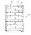
- FIG. 1shows a process stage in the course of the manufacture of a chip-stack arrangement 20 that is represented in FIG. 3 in its final state.
- two flexibly constructed carrier substrate 21 , 22are arranged with their conducting-path structures 24 , 25 , comprising a plurality of conducting paths 23 , located opposite one another.
- the ends 26 , 27 of the carrier substrates 21 , 22are accommodated in a clamping device 28 .
- the clamping device 28comprises in the present case a spacer block 29 , against which the ends 26 , 27 of the carrier substrates 21 and 22 respectively are held clamped by clamping jaws 30 , 31 .
- the spacer block 29is so dimensioned that a first chip 32 can be positioned in the manner represented in FIG. 1 between the carrier substrates 21 , 22 with its peripheral connection surfaces 33 , here in two rows extending perpendicular to the plane of the drawing, adjacent to the conducting paths 23 of the conducting-path structures 24 , 25 .
- the chip 32rests with its reverse side in contact with the spacer block 29 of the clamping device 28 .
- connection surfaces 33 of the chip 32are provided via soldered connections 34 consisting of a remelted deposit of soldering material 35 with a view to forming an electronically conductive connection between the connection surfaces 33 and the assigned conducting paths 23 of the conducting path structures 24 and 25 .
- the chip-stack arrangement 20(FIG. 3) is constructed in the manner of a sandwich from an alternating arrangement of the additional chips 36 to 39 and intermediate layers of adhesive 40 to 43 .
- These layers of adhesive 40 43serve, on the one hand, to form a spacer device between adjacent chips 32 , 36 and 36 , 37 and 37 , 38 and 39 and also, on the other hand, on account of the flexibility carrier substrates 21 , 22 , to bring about relative fixation of the entire arrangement.
- the deposits of solder material 35 for producing the soldered connections 34are placed individually in positionally precise manner in the connecting region 45 between the connection surfaces 33 and the conducting paths 23 by means of a tool that takes th form of an application capillary 44 .
- the necessary thermal energy for establishing the soldered connection by remeltingmay, with appropriate design of the application capillary 44 as a thermode device, be effected by the latter itself or also by a remelting device that is separate from it.
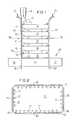
- FIG. 2 of a chip 53With the aid of the top view illustrated in FIG. 2 of a chip 53 , at the same time a variant differing from the representation of the chip-stack arrangement 20 in FIG. 3 for the purpose of forming a chip-stack arrangement 46 illustrated in FIG. 4 is represented in which, differing from the representation in FIG. 1, in addition to the two carrier substrates 21 , 22 arranged in opposing manner, which here are assigned to transverse sides 47 , 28 of the chip 53 , two further carrier substrates 49 , 50 are provided which are assigned to longitudinal sides 51 , 52 of the chip 53 .
- the chip-stack arrangement 46 represented in FIGS. 2 and 4 with here a total of four carrier substrates 21 , 22 and 49 , 50is suitable, as is clearly evident from FIG. 2, for combination with chips of the same type as the chip 53 that are provided not only with two rows of peripheral connection surfaces 33 , arranged in opposing manner, but moreover with two additional peripheral rows of connection surfaces 54 , arranged in opposing manner.
- connection surfaces 54 of the chip 53are, like the connection surfaces 33 of the chip 53 , also connected via soldered connections 34 to the conducting paths 23 of the carrier substrates 21 , 22 and 49 , 50 .
- soldered connections 34to the conducting paths 23 of the carrier substrates 21 , 22 and 49 , 50 .
- conductive adhesivesmay also be employed.
- the chip-stack arrangementis built up in the manner represented in FIG. 1-that is to say, by means of a sandwich-type layering of the chips.
- a chip-stack arrangementcan also be built up with only one carrier substrate.
- the chip-stack arrangementcan also be built up with an orientation differing from the orientation of the carrier substrates 21 , 22 represented in FIG. 1-for example, with horizontal alignment of the carrier substrate or substrates.
- the structure of a chip-stack arrangement 20represented by way of example in FIG. 1 enables a component test of the individual chips 32 to 39 that takes place almost simultaneously with the composition of the chip-stack arrangement.
- an electrical examination of the particular chip last insertedis carried out via the conducting paths 23 of the carrier substrates 21 , 22 .
- test device suitable for this purposecan be connected as a separate device to the ends 26 and 27 of the carrier substrates 21 , 22 that are clamped in the clamping device 28 .
- the clamping device 28in particular the spacer block 29 of the clamping device 28 , as an electrical test device or at least as a contact device for an electrical test device.
- FIG. 1 for the formation of a chip-stack arrangement 20enables, in particularly simple manner, a continuous manufacture of chip-stack arrangements 20 .
- the carrier substrates 21 and 22are held ready in the form of endless substrates arranged on rollers or a similar supply device and are moved forward one carrier-substrate section 99 , 100 at a time following a release of the clamping device 28 , the carrier-substrate sections 99 , 100 being so dimensioned that the desired number of chips can be arranged between the carrier-substrate sections 99 , 100 with a view to forming the chip-stack arrangement 20 .
- the carrier-substrate sections 99 , 100 which are now connected to the chipsare separated by means of a suitable separating device, which is not represented here, adjacent to the clamping device 28 so that, as a result of a further feed movement, the next carrier-substrate sections 99 , 100 can be equipped with chips.
- the chip-stack arrangement 20 or 46may be sealed at least to one side with a printed circuit board 55 or 56 respectively which, as represented by way of example in FIGS. 3 and 4, may be provided with an external contact-surface arrangement 57 or 58 in the manner of a “ball-grid array”.
- a printed circuit board 55 or another device enabling an external contact-surface arrangementcan be arranged both at the upper and at the lower end of a chip-stack arrangement 20 or 46 .
- the chip-stack arrangement 20 or 46is filled out in the chip interspaces 66 represented in FIG. 3 on the basis of an example of the chip-stack arrangement 20 with a sealing material which, furthermore, may also additionally encase the carrier substrates.
- Chip-stack arrangements that are encased and provided with an external contact-surface arrangementcan be used to particular advantage in connection with SMD technology.
- FIG. 5shows, represented by fully drawn lines, a flexible carrier substrate 67 in a representation that is spread out in the plane, in which an external contact-surface arrangement 68 is formed integrally in a flexible carrier layer 69 of the carrier substrate 67 .
- the conducting-path structure 71that is composed of individual conducting paths 70 merges in the end region of the carrier substrate 67 with a connection conducting-path structure 72 .
- the connection conducting-path structure 72comprises contact paths 73 which are arranged on the same side of the carrier layer 69 as the conducting paths 70 of the conducting-path structure 71 .
- On the opposite side of the carrier layer 69located opposite the free ends of the contact paths 73 , external contact surfaces are provided that are formed here by soldering points 74 which are connected to the contact paths 73 via through-contacts that are not represented in any detail.
- the carrier substrate 67 represented in FIG. 5 by solid linesenables, analogously to the two carrier substrates 21 , 22 represented in FIG. 1, the combination of several chips 32 and 36 to 39 so as to form a chip-stack arrangement, whereby the carrier substrate 67 represented by solid lines is suitable for combination with chips that, like the chips 32 and 36 to 39 represented in FIG. 1, comprise two opposite rows of peripheral connection surfaces.
- the carrier substrate 67which is provided with a total of 32 conducting paths 23 , is suitable to connect chips comprising 16 peripheral connection surfaces in each of two opposite rows.
- the connection of the chip-connection surfaces to the conducting paths 23can be effected in a manner analogous to that elucidated with reference to FIG. 1. As indicated in FIG.
- a carrier substratewhich in the manner of the carrier substrate 67 is provided with an integrated arrangement of external-contact connection surfaces can also be sued for equipping with chips comprising a total of four rows of peripheral connections. In this case additional external contact surfaces are then to be provided in the external contact-surface arrangement.
- FIG. 6shows, here by way of example with reference to the case of a chip-stack arrangement with two carrier substrates 21 , 22 , another possibility for forming an external contact-surface arrangement 75 .
- the carrier-substrate ends 76 , 77 of the carrier substrates 21 , 22are folded over in the direction of the upper side or contact-surface side of the chip 39 .
- an adhesive spacer device 78is interposed for example in the manner of the spacer devices 40 to 43 of the arrangement represented in FIG. 1.
- the conducting paths 23are through-contacted in the region of the carrier-substrate ends 76 , 77 onto the reverse side of the carrier substrates 21 , 22 .
- Thiscan be effected by application and remelting of solder balls in carrier-layer recesses which open out on to the reverse side of the conducting path 23 , so that, as represented in FIG. 6, the external contact surfaces of the external contact-surface arrangement are formed by soldering points 79 .
Landscapes
- Engineering & Computer Science (AREA)
- Power Engineering (AREA)
- Microelectronics & Electronic Packaging (AREA)
- Physics & Mathematics (AREA)
- Condensed Matter Physics & Semiconductors (AREA)
- General Physics & Mathematics (AREA)
- Computer Hardware Design (AREA)
- Wire Bonding (AREA)
- Combinations Of Printed Boards (AREA)
Abstract
Description
- This is a division of application Ser. No. 08/847,961 filed Apr. 22, 1997 which is incorporated herein by reference in its entirety. Ser. No. 09/553,123 filed Apr. 19, 2000, is also a division of application 08/847,961, which is still pending. The present invention relates to a process for the formation of a spatial chip arrangement having several chips arranged in several planes and electrically connected to one another, in which the chips are connected via their peripheral connection surfaces to assigned conducting paths of a conducting-path structure which is arranged on at least one carrier substrate by the chips being arranged transverse to the longitudinal extent of the carrier substrate.[0001]
- With the increasing miniaturisation of electronic appliances such as portable telephone for example, also generally designated as “handy”, or portable computers, known by the expression “notebook”, the demands regarding integration density of the electronic modules employed therein also increase. To a particular degree this is unquestionably the case with memory modules which are utilized in such appliances or memory expansions which may be used optionally. At the present time, by way of structural design for such highly integrated memory modules use is made as a rule of so-called “multi-chip modules” (MCM) in which the individual chips are arranged above one another and electrically connected to one another. By reason of the high integration density-that is to say, the arrangement of a plurality of chips within an extremely small space-the probability of failure of such a memory module also increases of course, since for failure of a component it is sufficient if only one of the chips which are processed in a plurality is defective. In order to be able to eliminate failure of a component to the greatest possible extent during operation of the highly integrated modules, an examination of the modules has hitherto been undertaken after completion and prior to delivery or incorporation into the electronic appliance in question. This is associated, on the one hand, with an additional component test following the actual manufacturing process. On the other hand, the implementation of a component test only after finishing the complete component means that in the event of a component failure, which as a rule is caused only by the failure of an individual chip, the entire component is rejected.[0002]
- The object underlying the present invention is therefore to propose a process for the formation of a spatial chip arrangement despite the fact that a high integration density is achieved, creates an opportunity for the early detection of faults so that classification of the complete component as a reject can be prevented to the greatest possible extent.[0003]
- In accordance with the invention it is proposed, with a view to forming a spatial chip arrangement having several chips arranged in various planes and electrically connected to one another, to contact the chips via the peripheral connecting surfaces with assigned conducting paths of a conducting-path structure that is arranged on at least one carrier substrate. In this regard the chips will be arranged transverse to the rectilinearly aligned carrier substrate.[0004]
- The invention offers, on the one hand, the possibility of arranging the chips in a space-saving structure and, on the other hand, the possibility of a simple electrical examination, during manufacture of the stacked chip arrangement, of the chip that is connected to the carrier substrate.[0005]
- The space-saving arrangement of the chips is created by the transverse arrangement of the chips.[0006]
- A particularly high integration density can be produced by the chips being brought with their peripheral connection surfaces arranged along a lateral edge into a connecting position adjacent to the conducting paths and transverse to the longitudinal extent of the conducting paths and then by a connection being effected between pairings, assigned respectively to one another, of conducting path an connection surface via a connecting material that is applied between the respective conducting path and the assigned connection surface.[0007]
- The implementation of the process proves to be particularly advantageous if, after a chip has been brought into contact with the carrier substrate, an electrical examination of the chip is carried out via the connecting-path structure of the carrier substrate that is connected to a test device.[0008]
- It proves to be advantageous if, with a view to preparing the contacting of the chips, the carrier substrate or substrates is/are fixed with one end in a clamping device. Hence the clamping device may also be used as a test device.[0009]
- In particular in the case where it is a question of chips with reverse-side metallisation it proves to be advantageous if in each case prior to making contact with an additional chip a spacer device is arranged on the upper side of the previously contacted chip. On one the hand, given a suitable choice of material for the spacer device, an insulation between the chips is achieved. On the other hand, a static arrangement is also made possible. This stabilisation effect can be intensified still further if an adhesive material, for example an application of adhesive, is chosen for the spacer device.[0010]
- In the case where a soldering material is used by way of connecting material it proves to be advantageous if the connecting material is applied in the form of isolated deposits of connecting material onto the conducting paths and/or the connecting surfaces and is then activated by remelting.[0011]
- In order, finally, to enable an to external contracting of the spatial chip arrangement that is as simple as possible, it proves to be particularly advantageous if, after the last chip has been brought into contact, a projecting length of the carrier substrate is firstly folded over the upper side of the chip and connected to the upper side and then a through-contact is made from the reverse side of the carrier substrate that is connected to the chip-connection surfaces. Alternatively it is also possible to make use, right from the beginning, of carrier substrates that are provided with an appropriate through-contact.[0012]
- An advantageous alternative to this is obtained if, with a view to forming an external-contact arrangement on the chip arrangement prior to contacting the first chip or after contacting the last chip, a printed circuit board or a modified chip having an external-contact arrangement arranged on the outside and distributed in planar manner is contacted with the conducting paths of the carrier substrate via internal contacts arranged on the periphery of the printed circuit board or on the periphery of the chip and connected to the external-contact arrangement by means of a connection conducting-path structure.[0013]
- In order to achieve a chip arrangement that is sealed off from environmental influence to the greatest possible extent and that has, moreover, a mechanical stability that is as great as possible, it is advantageous if, after contacting the desired number of chips, the chip arrangement produced is sealed with a view to forming a casing.[0014]
- Other objects and features of the present invention will become apparent from the following detailed description considered in conjunction with the accompanying drawings. It is to be understood, however, that the drawings are intended solely for purposes of illustration and not as a definition of the limits of the invention, for which reference should be made to the appended claims.[0015]
- The embodiments of the spatial chip arrangement are illustrated in more detail below by illustrating the processes for its manufacture with reference to the drawings. In the drawings, wherein like reference numerals delineate similar elements throughout the several views:[0016]
- FIG. 1 an embodiment example of a stacked chip arrangement during manufacturing in a variant of the process according to the invention;[0017]
- FIG. 2 a top view of a chip represented in FIG. 1;[0018]
- FIG. 3 a side view of the now finished chip arrangement that is shown in FIG. 1 during the manufacturing process;[0019]
- FIG. 4 a top view of a chip arrangement that is slightly modified in comparison with FIG. 3;[0020]
- FIG. 5 the representation of a carrier substrate for the formation of a chip arrangement;[0021]
- FIG. 6 a partial side view of a chip arrangement corresponding to FIG. 3.[0022]
- FIG. 1 shows a process stage in the course of the manufacture of a chip-[0023]
stack arrangement 20 that is represented in FIG. 3 in its final state. With a view to forming the chip-stack arrangement20 (FIG. 3), in the case of the embodiment example currently represented two flexibly constructedcarrier substrate path structures paths 23, located opposite one another. With a view to fixing thecarrier substrates ends carrier substrates clamping device 28. Theclamping device 28 comprises in the present case aspacer block 29, against which theends carrier substrates jaws spacer block 29 is so dimensioned that afirst chip 32 can be positioned in the manner represented in FIG. 1 between thecarrier substrates peripheral connection surfaces 33, here in two rows extending perpendicular to the plane of the drawing, adjacent to theconducting paths 23 of the conducting-path structures - For this purpose the[0024]
chip 32 rests with its reverse side in contact with thespacer block 29 of theclamping device 28. - In the case of the configuration represented in FIG. 1 the[0025]
connection surfaces 33 of thechip 32 are provided via solderedconnections 34 consisting of a remelted deposit of solderingmaterial 35 with a view to forming an electronically conductive connection between theconnection surfaces 33 and the assigned conductingpaths 23 of the conductingpath structures - From FIG. 1 it becomes clear that the chip-stack arrangement[0026]20 (FIG. 3) is constructed in the manner of a sandwich from an alternating arrangement of the
additional chips 36 to39 and intermediate layers ofadhesive 40 to43. These layers of adhesive4043 serve, on the one hand, to form a spacer device betweenadjacent chips flexibility carrier substrates - As can be further gathered from FIG. 1, as represented in FIG. 1 on the basis of an example fo the connection of the[0027]
topmost chip 39, the deposits ofsolder material 35 for producing the solderedconnections 34 are placed individually in positionally precise manner in the connectingregion 45 between theconnection surfaces 33 and the conductingpaths 23 by means of a tool that takes th form of anapplication capillary 44. The necessary thermal energy for establishing the soldered connection by remelting may, with appropriate design of the application capillary44 as a thermode device, be effected by the latter itself or also by a remelting device that is separate from it. - With the aid of the top view illustrated in FIG. 2 of a[0028]
chip 53, at the same time a variant differing from the representation of the chip-stack arrangement 20 in FIG. 3 for the purpose of forming a chip-stack arrangement 46 illustrated in FIG. 4 is represented in which, differing from the representation in FIG. 1, in addition to the twocarrier substrates transverse sides chip 53, twofurther carrier substrates longitudinal sides chip 53. - The chip-[0029]
stack arrangement 46 represented in FIGS. 2 and 4 with here a total of fourcarrier substrates chip 53 that are provided not only with two rows ofperipheral connection surfaces 33, arranged in opposing manner, but moreover with two additional peripheral rows ofconnection surfaces 54, arranged in opposing manner. - Corresponding to the remarks made with reference to FIG. 1, the[0030]
connection surfaces 54 of thechip 53 are, like theconnection surfaces 33 of thechip 53, also connected via solderedconnections 34 to the conductingpaths 23 of thecarrier substrates connection surfaces - Irrespective of whether, with respect to the particular embodiment, it is a question of a chip-[0031]
stack arrangement 20 or a chip-stack arrangement 46, the chip-stack arrangement is built up in the manner represented in FIG. 1-that is to say, by means of a sandwich-type layering of the chips. In this regard it is advisable, with a view to increasing the mechanical stability of the entire chip-stack arrangement carrier substrates individual chips 32 to39 or53 to one another by means ofspacer devices 40 to43 of adhesive design. - In the case where use is made of inherently rigid carrier substrates it is possible to dispense with said devices. Depending on the configuration of the connection surfaces of the chips that are to be integrated into a chip-stack arrangement, a chip-stack arrangement can also be built up with only one carrier substrate. In the case of carrier substrates of inherently rigid design the chip-stack arrangement can also be built up with an orientation differing from the orientation of the[0032]
carrier substrates - Irrespective to the construction of the carrier substrates that are used in order to build up a chip-stack arrangement, the structure of a chip-[0033]
stack arrangement 20 represented by way of example in FIG. 1 enables a component test of theindividual chips 32 to39 that takes place almost simultaneously with the composition of the chip-stack arrangement. For this purpose, after each application of an individual chip starting withchip 32 and completion of the electrically conductive connections-here taking the form of a soldered connection34-to the conductingpaths 23 of thecarrier substrates paths 23 of thecarrier substrates ends carrier substrates clamping device 28. But there is also the possibility of designing theclamping device 28, in particular thespacer block 29 of theclamping device 28, as an electrical test device or at least as a contact device for an electrical test device. - The arrangement represented in FIG. 1 for the formation of a chip-[0034]
stack arrangement 20 enables, in particularly simple manner, a continuous manufacture of chip-stack arrangements 20. To this end thecarrier substrates substrate section clamping device 28, the carrier-substrate sections substrate sections stack arrangement 20. After completion of the arrangement the carrier-substrate sections clamping device 28 so that, as a result of a further feed movement, the next carrier-substrate sections - In order to simplify contacting of the finished chip-[0035]
stack arrangement stack arrangement circuit board surface arrangement - As becomes clear in particular from the top view represented in FIG. 4, for the purpose of connection to the printed[0036]
circuit board 56 the upper ends of thecarrier substrates circuit board 56 in such a way that the conductingpaths 23 of thecarrier substrates circuit board 56. From the internal contact surfaces63 contact paths64 lead to the individual external contact surfaces65 of the printedcircuit board 56 that are configured in the external contact-surface arrangement 58 described previously. - As FIG. 3 shows, a printed[0037]
circuit board 55 or another device enabling an external contact-surface arrangement can be arranged both at the upper and at the lower end of a chip-stack arrangement chips stack arrangement 20 or in the chip-stack arrangement 20 or in the chip-stack arrangement 46, the chip-stack arrangement stack arrangement 20 with a sealing material which, furthermore, may also additionally encase the carrier substrates. Chip-stack arrangements that are encased and provided with an external contact-surface arrangement can be used to particular advantage in connection with SMD technology. - FIG. 5 shows, represented by fully drawn lines, a[0038]
flexible carrier substrate 67 in a representation that is spread out in the plane, in which an external contact-surface arrangement 68 is formed integrally in aflexible carrier layer 69 of thecarrier substrate 67. To this end the conducting-path structure 71 that is composed ofindividual conducting paths 70 merges in the end region of thecarrier substrate 67 with a connection conducting-path structure 72. The connection conducting-path structure 72 comprisescontact paths 73 which are arranged on the same side of thecarrier layer 69 as the conductingpaths 70 of the conducting-path structure 71. On the opposite side of thecarrier layer 69, located opposite the free ends of thecontact paths 73, external contact surfaces are provided that are formed here by solderingpoints 74 which are connected to thecontact paths 73 via through-contacts that are not represented in any detail. - The[0039]
carrier substrate 67 represented in FIG. 5 by solid lines enables, analogously to the twocarrier substrates several chips carrier substrate 67 represented by solid lines is suitable for combination with chips that, like thechips carrier substrate 67, which is provided with a total of32 conductingpaths 23, is suitable to connect chips comprising16 peripheral connection surfaces in each of two opposite rows. The connection of the chip-connection surfaces to the conductingpaths 23 can be effected in a manner analogous to that elucidated with reference to FIG. 1. As indicated in FIG. 5 by twolateral strands principal strand 96 of thecarrier substrate 61 and represented by a dashed line, a carrier substrate which in the manner of thecarrier substrate 67 is provided with an integrated arrangement of external-contact connection surfaces can also be sued for equipping with chips comprising a total of four rows of peripheral connections. In this case additional external contact surfaces are then to be provided in the external contact-surface arrangement. - FIG. 6 shows, here by way of example with reference to the case of a chip-stack arrangement with two[0040]
carrier substrates surface arrangement 75. With a view to forming the external contact-surface arrangement 75, after establishing the contact of the conductingpaths 23 with connection surfaces33 of anuppermost chip 39 the carrier-substrate ends76,77 of thecarrier substrates chip 39. For defined positioning of the carrier-substrate ends76,77 and securing thereof in relation to thechip 39 anadhesive spacer device 78 is interposed for example in the manner of thespacer devices 40 to43 of the arrangement represented in FIG. 1. - With a view to forming the external contact-[0041]
surface arrangement 75 the conductingpaths 23 are through-contacted in the region of the carrier-substrate ends76,77 onto the reverse side of thecarrier substrates path 23, so that, as represented in FIG. 6, the external contact surfaces of the external contact-surface arrangement are formed by soldering points79. - Thus, while there have been shown and described and pointed out fundamental novel features of the invention as applied to a preferred embodiment thereof, it will be understood that various omissions and substitutions and changes in the form and details of the devices illustrated, and in their operation, may be made by those skilled in the art without departing from the spirit of the invention. For example, it is expressly intended that all combinations of those elements and/or method steps which perform substantially the same function in substantially the same way to achieve the same results are within the scope of the invention. Substitutions of elements from one described embodiment to another are also fully intended and contemplated. It is also to be understood that the drawings are not necessarily drawn to scale but that they are merely conceptual in nature. It is the intention, therefore, to be limited only as indicated by the scope of the claims appended hereto.[0042]
Claims (11)
Priority Applications (1)
| Application Number | Priority Date | Filing Date | Title |
|---|---|---|---|
| US09/962,553US7087442B2 (en) | 1996-06-28 | 2001-09-24 | Process for the formation of a spatial chip arrangement and spatial chip arrangement |
Applications Claiming Priority (5)
| Application Number | Priority Date | Filing Date | Title |
|---|---|---|---|
| DE19626126.0 | 1996-06-28 | ||
| DE19626126ADE19626126C2 (en) | 1996-06-28 | 1996-06-28 | Method for forming a spatial chip arrangement and spatial chip arrangement |
| US08/847,961US6281577B1 (en) | 1996-06-28 | 1997-04-22 | Chips arranged in plurality of planes and electrically connected to one another |
| US55312300A | 2000-04-19 | 2000-04-19 | |
| US09/962,553US7087442B2 (en) | 1996-06-28 | 2001-09-24 | Process for the formation of a spatial chip arrangement and spatial chip arrangement |
Related Parent Applications (1)
| Application Number | Title | Priority Date | Filing Date |
|---|---|---|---|
| US55312300ADivision | 1996-06-28 | 2000-04-19 |
Publications (2)
| Publication Number | Publication Date |
|---|---|
| US20020009828A1true US20020009828A1 (en) | 2002-01-24 |
| US7087442B2 US7087442B2 (en) | 2006-08-08 |
Family
ID=7798388
Family Applications (2)
| Application Number | Title | Priority Date | Filing Date |
|---|---|---|---|
| US08/847,961Expired - LifetimeUS6281577B1 (en) | 1996-06-28 | 1997-04-22 | Chips arranged in plurality of planes and electrically connected to one another |
| US09/962,553Expired - Fee RelatedUS7087442B2 (en) | 1996-06-28 | 2001-09-24 | Process for the formation of a spatial chip arrangement and spatial chip arrangement |
Family Applications Before (1)
| Application Number | Title | Priority Date | Filing Date |
|---|---|---|---|
| US08/847,961Expired - LifetimeUS6281577B1 (en) | 1996-06-28 | 1997-04-22 | Chips arranged in plurality of planes and electrically connected to one another |
Country Status (6)
| Country | Link |
|---|---|
| US (2) | US6281577B1 (en) |
| EP (1) | EP0847597A1 (en) |
| JP (1) | JP3739013B2 (en) |
| KR (1) | KR100595047B1 (en) |
| DE (1) | DE19626126C2 (en) |
| WO (1) | WO1998000868A1 (en) |
Cited By (3)
| Publication number | Priority date | Publication date | Assignee | Title |
|---|---|---|---|---|
| US20040056342A1 (en)* | 2002-05-08 | 2004-03-25 | Cobbley Chad A. | Stacked die module and techniques for forming a stacked die module |
| US20060008946A1 (en)* | 2002-08-28 | 2006-01-12 | Micron Technology, Inc. | Castellation wafer level packaging of integrated circuit chips |
| US11367709B2 (en)* | 2018-06-05 | 2022-06-21 | PAC Tech—Packaging Technologies GmbH | Semiconductor chip stack arrangement and semiconductor chip for producing such a semiconductor chip stack arrangement |
Families Citing this family (132)
| Publication number | Priority date | Publication date | Assignee | Title |
|---|---|---|---|---|
| KR100304959B1 (en)* | 1998-10-21 | 2001-09-24 | 김영환 | Chip stacked semiconductor package and manufacturing method thereof |
| US6323060B1 (en) | 1999-05-05 | 2001-11-27 | Dense-Pac Microsystems, Inc. | Stackable flex circuit IC package and method of making same |
| JP3694825B2 (en)* | 1999-11-18 | 2005-09-14 | 日本航空電子工業株式会社 | Conductive pattern forming method and connector, flexible printed wiring board, anisotropic conductive member |
| US6262895B1 (en)* | 2000-01-13 | 2001-07-17 | John A. Forthun | Stackable chip package with flex carrier |
| JP2001352035A (en)* | 2000-06-07 | 2001-12-21 | Sony Corp | Assembling jig for multilayer semiconductor device and manufacturing method therefor |
| US6461881B1 (en) | 2000-06-08 | 2002-10-08 | Micron Technology, Inc. | Stereolithographic method and apparatus for fabricating spacers for semiconductor devices and resulting structures |
| US6576494B1 (en)* | 2000-06-28 | 2003-06-10 | Micron Technology, Inc. | Recessed encapsulated microelectronic devices and methods for formation |
| US6560117B2 (en)* | 2000-06-28 | 2003-05-06 | Micron Technology, Inc. | Packaged microelectronic die assemblies and methods of manufacture |
| US6552910B1 (en) | 2000-06-28 | 2003-04-22 | Micron Technology, Inc. | Stacked-die assemblies with a plurality of microelectronic devices and methods of manufacture |
| FI111197B (en)* | 2000-07-12 | 2003-06-13 | Nokia Oyj | Multichip module |
| US7298031B1 (en) | 2000-08-09 | 2007-11-20 | Micron Technology, Inc. | Multiple substrate microelectronic devices and methods of manufacture |
| US6607937B1 (en)* | 2000-08-23 | 2003-08-19 | Micron Technology, Inc. | Stacked microelectronic dies and methods for stacking microelectronic dies |
| GB0029312D0 (en) | 2000-12-01 | 2001-01-17 | Philips Corp Intellectual Pty | Flexible electronic device |
| US6884653B2 (en)* | 2001-03-21 | 2005-04-26 | Micron Technology, Inc. | Folded interposer |
| DE10125497C2 (en)* | 2001-05-23 | 2003-06-05 | Pac Tech Gmbh | Method for producing a contact substrate and contact substrate |
| DE10136655C1 (en)* | 2001-07-20 | 2002-08-01 | Optosys Technologies Gmbh | Multichip module in COB design, in particular CompactFlash card with high storage capacity and method for producing the same |
| US6627984B2 (en)* | 2001-07-24 | 2003-09-30 | Dense-Pac Microsystems, Inc. | Chip stack with differing chip package types |
| US20030038356A1 (en)* | 2001-08-24 | 2003-02-27 | Derderian James M | Semiconductor devices including stacking spacers thereon, assemblies including the semiconductor devices, and methods |
| SG111919A1 (en)* | 2001-08-29 | 2005-06-29 | Micron Technology Inc | Packaged microelectronic devices and methods of forming same |
| US20030042615A1 (en) | 2001-08-30 | 2003-03-06 | Tongbi Jiang | Stacked microelectronic devices and methods of fabricating same |
| US6950312B2 (en)* | 2001-10-02 | 2005-09-27 | International Business Machines Corporation | Electronic units and method for packaging and assembly of said electronic units |
| US6747348B2 (en)* | 2001-10-16 | 2004-06-08 | Micron Technology, Inc. | Apparatus and method for leadless packaging of semiconductor devices |
| US7026708B2 (en) | 2001-10-26 | 2006-04-11 | Staktek Group L.P. | Low profile chip scale stacking system and method |
| US6940729B2 (en) | 2001-10-26 | 2005-09-06 | Staktek Group L.P. | Integrated circuit stacking system and method |
| US7053478B2 (en) | 2001-10-26 | 2006-05-30 | Staktek Group L.P. | Pitch change and chip scale stacking system |
| US6576992B1 (en)* | 2001-10-26 | 2003-06-10 | Staktek Group L.P. | Chip scale stacking system and method |
| US7371609B2 (en) | 2001-10-26 | 2008-05-13 | Staktek Group L.P. | Stacked module systems and methods |
| US20060255446A1 (en)* | 2001-10-26 | 2006-11-16 | Staktek Group, L.P. | Stacked modules and method |
| US6914324B2 (en) | 2001-10-26 | 2005-07-05 | Staktek Group L.P. | Memory expansion and chip scale stacking system and method |
| US7656678B2 (en) | 2001-10-26 | 2010-02-02 | Entorian Technologies, Lp | Stacked module systems |
| US20030234443A1 (en) | 2001-10-26 | 2003-12-25 | Staktek Group, L.P. | Low profile stacking system and method |
| US7310458B2 (en) | 2001-10-26 | 2007-12-18 | Staktek Group L.P. | Stacked module systems and methods |
| US7485951B2 (en) | 2001-10-26 | 2009-02-03 | Entorian Technologies, Lp | Modularized die stacking system and method |
| US7202555B2 (en) | 2001-10-26 | 2007-04-10 | Staktek Group L.P. | Pitch change and chip scale stacking system and method |
| US6956284B2 (en) | 2001-10-26 | 2005-10-18 | Staktek Group L.P. | Integrated circuit stacking system and method |
| DE10164800B4 (en)* | 2001-11-02 | 2005-03-31 | Infineon Technologies Ag | Method for producing an electronic component with a plurality of chips stacked on top of one another and contacted with one another |
| US7081373B2 (en) | 2001-12-14 | 2006-07-25 | Staktek Group, L.P. | CSP chip stack with flex circuit |
| US6750547B2 (en)* | 2001-12-26 | 2004-06-15 | Micron Technology, Inc. | Multi-substrate microelectronic packages and methods for manufacture |
| US6896760B1 (en)* | 2002-01-16 | 2005-05-24 | Micron Technology, Inc. | Fabrication of stacked microelectronic devices |
| US6958533B2 (en)* | 2002-01-22 | 2005-10-25 | Honeywell International Inc. | High density 3-D integrated circuit package |
| US7198693B1 (en) | 2002-02-20 | 2007-04-03 | Micron Technology, Inc. | Microelectronic device having a plurality of stacked dies and methods for manufacturing such microelectronic assemblies |
| US7109588B2 (en) | 2002-04-04 | 2006-09-19 | Micron Technology, Inc. | Method and apparatus for attaching microelectronic substrates and support members |
| US6903001B2 (en)* | 2002-07-18 | 2005-06-07 | Micron Technology Inc. | Techniques to create low K ILD for BEOL |
| SG120879A1 (en)* | 2002-08-08 | 2006-04-26 | Micron Technology Inc | Packaged microelectronic components |
| SG114585A1 (en)* | 2002-11-22 | 2005-09-28 | Micron Technology Inc | Packaged microelectronic component assemblies |
| SG143931A1 (en) | 2003-03-04 | 2008-07-29 | Micron Technology Inc | Microelectronic component assemblies employing lead frames having reduced-thickness inner lengths |
| SG137651A1 (en)* | 2003-03-14 | 2007-12-28 | Micron Technology Inc | Microelectronic devices and methods for packaging microelectronic devices |
| US6841029B2 (en)* | 2003-03-27 | 2005-01-11 | Advanced Cardiovascular Systems, Inc. | Surface modification of expanded ultra high molecular weight polyethylene (eUHMWPE) for improved bondability |
| US20040233641A1 (en)* | 2003-05-19 | 2004-11-25 | Mark Moshayedi | Processor/memory module with foldable substrate |
| US7071421B2 (en) | 2003-08-29 | 2006-07-04 | Micron Technology, Inc. | Stacked microfeature devices and associated methods |
| US7368810B2 (en)* | 2003-08-29 | 2008-05-06 | Micron Technology, Inc. | Invertible microfeature device packages |
| US7542304B2 (en) | 2003-09-15 | 2009-06-02 | Entorian Technologies, Lp | Memory expansion and integrated circuit stacking system and method |
| US7091124B2 (en) | 2003-11-13 | 2006-08-15 | Micron Technology, Inc. | Methods for forming vias in microelectronic devices, and methods for packaging microelectronic devices |
| US8084866B2 (en)* | 2003-12-10 | 2011-12-27 | Micron Technology, Inc. | Microelectronic devices and methods for filling vias in microelectronic devices |
| US20050104171A1 (en)* | 2003-11-13 | 2005-05-19 | Benson Peter A. | Microelectronic devices having conductive complementary structures and methods of manufacturing microelectronic devices having conductive complementary structures |
| DE102004005586B3 (en)* | 2004-02-04 | 2005-09-29 | Infineon Technologies Ag | Semiconductor device having a semiconductor chip stack on a rewiring plate and producing the same |
| US7253089B2 (en)* | 2004-06-14 | 2007-08-07 | Micron Technology, Inc. | Microfeature devices and methods for manufacturing microfeature devices |
| SG145547A1 (en) | 2004-07-23 | 2008-09-29 | Micron Technology Inc | Microelectronic component assemblies with recessed wire bonds and methods of making same |
| US7602618B2 (en)* | 2004-08-25 | 2009-10-13 | Micron Technology, Inc. | Methods and apparatuses for transferring heat from stacked microfeature devices |
| US7511968B2 (en) | 2004-09-03 | 2009-03-31 | Entorian Technologies, Lp | Buffered thin module system and method |
| US7443023B2 (en) | 2004-09-03 | 2008-10-28 | Entorian Technologies, Lp | High capacity thin module system |
| US7324352B2 (en) | 2004-09-03 | 2008-01-29 | Staktek Group L.P. | High capacity thin module system and method |
| US7446410B2 (en) | 2004-09-03 | 2008-11-04 | Entorian Technologies, Lp | Circuit module with thermal casing systems |
| US7542297B2 (en) | 2004-09-03 | 2009-06-02 | Entorian Technologies, Lp | Optimized mounting area circuit module system and method |
| US20060050492A1 (en) | 2004-09-03 | 2006-03-09 | Staktek Group, L.P. | Thin module system and method |
| US7423885B2 (en) | 2004-09-03 | 2008-09-09 | Entorian Technologies, Lp | Die module system |
| US7616452B2 (en) | 2004-09-03 | 2009-11-10 | Entorian Technologies, Lp | Flex circuit constructions for high capacity circuit module systems and methods |
| US7606040B2 (en) | 2004-09-03 | 2009-10-20 | Entorian Technologies, Lp | Memory module system and method |
| US7289327B2 (en) | 2006-02-27 | 2007-10-30 | Stakick Group L.P. | Active cooling methods and apparatus for modules |
| US7606050B2 (en) | 2004-09-03 | 2009-10-20 | Entorian Technologies, Lp | Compact module system and method |
| US7468893B2 (en) | 2004-09-03 | 2008-12-23 | Entorian Technologies, Lp | Thin module system and method |
| US7606049B2 (en) | 2004-09-03 | 2009-10-20 | Entorian Technologies, Lp | Module thermal management system and method |
| US7760513B2 (en) | 2004-09-03 | 2010-07-20 | Entorian Technologies Lp | Modified core for circuit module system and method |
| US7522421B2 (en) | 2004-09-03 | 2009-04-21 | Entorian Technologies, Lp | Split core circuit module |
| US7579687B2 (en) | 2004-09-03 | 2009-08-25 | Entorian Technologies, Lp | Circuit module turbulence enhancement systems and methods |
| US7309914B2 (en) | 2005-01-20 | 2007-12-18 | Staktek Group L.P. | Inverted CSP stacking system and method |
| US8278751B2 (en) | 2005-02-08 | 2012-10-02 | Micron Technology, Inc. | Methods of adhering microfeature workpieces, including a chip, to a support member |
| US7033861B1 (en) | 2005-05-18 | 2006-04-25 | Staktek Group L.P. | Stacked module systems and method |
| SG130055A1 (en)* | 2005-08-19 | 2007-03-20 | Micron Technology Inc | Microelectronic devices, stacked microelectronic devices, and methods for manufacturing microelectronic devices |
| SG130061A1 (en)* | 2005-08-24 | 2007-03-20 | Micron Technology Inc | Microelectronic devices and microelectronic support devices, and associated assemblies and methods |
| SG130066A1 (en)* | 2005-08-26 | 2007-03-20 | Micron Technology Inc | Microelectronic device packages, stacked microelectronic device packages, and methods for manufacturing microelectronic devices |
| US7807505B2 (en)* | 2005-08-30 | 2010-10-05 | Micron Technology, Inc. | Methods for wafer-level packaging of microfeature devices and microfeature devices formed using such methods |
| US20070045812A1 (en)* | 2005-08-31 | 2007-03-01 | Micron Technology, Inc. | Microfeature assemblies including interconnect structures and methods for forming such interconnect structures |
| US7745944B2 (en) | 2005-08-31 | 2010-06-29 | Micron Technology, Inc. | Microelectronic devices having intermediate contacts for connection to interposer substrates, and associated methods of packaging microelectronic devices with intermediate contacts |
| US7485969B2 (en)* | 2005-09-01 | 2009-02-03 | Micron Technology, Inc. | Stacked microelectronic devices and methods for manufacturing microelectronic devices |
| US20070045807A1 (en)* | 2005-09-01 | 2007-03-01 | Micron Technology, Inc. | Microelectronic devices and methods for manufacturing microelectronic devices |
| TWI306652B (en)* | 2005-10-28 | 2009-02-21 | Chipmos Technologies Inc | Light emitting diode package structure |
| US7576995B2 (en) | 2005-11-04 | 2009-08-18 | Entorian Technologies, Lp | Flex circuit apparatus and method for adding capacitance while conserving circuit board surface area |
| US20070148820A1 (en)* | 2005-12-22 | 2007-06-28 | Micron Technology, Inc. | Microelectronic devices and methods for manufacturing microelectronic devices |
| SG133445A1 (en)* | 2005-12-29 | 2007-07-30 | Micron Technology Inc | Methods for packaging microelectronic devices and microelectronic devices formed using such methods |
| US7605454B2 (en) | 2006-01-11 | 2009-10-20 | Entorian Technologies, Lp | Memory card and method for devising |
| US7304382B2 (en) | 2006-01-11 | 2007-12-04 | Staktek Group L.P. | Managed memory component |
| US7508069B2 (en) | 2006-01-11 | 2009-03-24 | Entorian Technologies, Lp | Managed memory component |
| US7508058B2 (en) | 2006-01-11 | 2009-03-24 | Entorian Technologies, Lp | Stacked integrated circuit module |
| US7608920B2 (en) | 2006-01-11 | 2009-10-27 | Entorian Technologies, Lp | Memory card and method for devising |
| US7511969B2 (en) | 2006-02-02 | 2009-03-31 | Entorian Technologies, Lp | Composite core circuit module system and method |
| SG135074A1 (en) | 2006-02-28 | 2007-09-28 | Micron Technology Inc | Microelectronic devices, stacked microelectronic devices, and methods for manufacturing such devices |
| SG135979A1 (en)* | 2006-03-08 | 2007-10-29 | Micron Technology Inc | Microelectronic device assemblies including assemblies with recurved leadframes, and associated methods |
| SG136009A1 (en) | 2006-03-29 | 2007-10-29 | Micron Technology Inc | Packaged microelectronic devices recessed in support member cavities, and associated methods |
| US7910385B2 (en) | 2006-05-12 | 2011-03-22 | Micron Technology, Inc. | Method of fabricating microelectronic devices |
| SG139573A1 (en)* | 2006-07-17 | 2008-02-29 | Micron Technology Inc | Microelectronic packages with leadframes, including leadframes configured for stacked die packages, and associated systems and methods |
| US7888185B2 (en)* | 2006-08-17 | 2011-02-15 | Micron Technology, Inc. | Semiconductor device assemblies and systems including at least one conductive pathway extending around a side of at least one semiconductor device |
| US7749882B2 (en)* | 2006-08-23 | 2010-07-06 | Micron Technology, Inc. | Packaged microelectronic devices and methods for manufacturing packaged microelectronic devices |
| US7868440B2 (en) | 2006-08-25 | 2011-01-11 | Micron Technology, Inc. | Packaged microdevices and methods for manufacturing packaged microdevices |
| US7468553B2 (en) | 2006-10-20 | 2008-12-23 | Entorian Technologies, Lp | Stackable micropackages and stacked modules |
| US7417310B2 (en) | 2006-11-02 | 2008-08-26 | Entorian Technologies, Lp | Circuit module having force resistant construction |
| SG143098A1 (en) | 2006-12-04 | 2008-06-27 | Micron Technology Inc | Packaged microelectronic devices and methods for manufacturing packaged microelectronic devices |
| US7750449B2 (en)* | 2007-03-13 | 2010-07-06 | Micron Technology, Inc. | Packaged semiconductor components having substantially rigid support members and methods of packaging semiconductor components |
| SG149726A1 (en) | 2007-07-24 | 2009-02-27 | Micron Technology Inc | Microelectronic die packages with metal leads, including metal leads for stacked die packages, and associated systems and methods |
| SG150396A1 (en)* | 2007-08-16 | 2009-03-30 | Micron Technology Inc | Microelectronic die packages with leadframes, including leadframe-based interposer for stacked die packages, and associated systems and methods |
| KR20090032845A (en)* | 2007-09-28 | 2009-04-01 | 삼성전자주식회사 | Semiconductor package and manufacturing method thereof |
| JP2009176815A (en)* | 2008-01-22 | 2009-08-06 | Olympus Corp | Mounting structure |
| US7972968B2 (en)* | 2008-08-18 | 2011-07-05 | Applied Materials, Inc. | High density plasma gapfill deposition-etch-deposition process etchant |
| US7872332B2 (en) | 2008-09-11 | 2011-01-18 | Micron Technology, Inc. | Interconnect structures for stacked dies, including penetrating structures for through-silicon vias, and associated systems and methods |
| US7557439B1 (en)* | 2008-09-29 | 2009-07-07 | Tdk Corporation | Layered chip package that implements memory device |
| US8314487B2 (en)* | 2009-12-18 | 2012-11-20 | Infineon Technologies Ag | Flange for semiconductor die |
| US8697457B1 (en)* | 2011-06-22 | 2014-04-15 | Bae Systems Information And Electronic Systems Integration Inc. | Devices and methods for stacking individually tested devices to form multi-chip electronic modules |
| US8796822B2 (en) | 2011-10-07 | 2014-08-05 | Freescale Semiconductor, Inc. | Stacked semiconductor devices |
| US9076664B2 (en) | 2011-10-07 | 2015-07-07 | Freescale Semiconductor, Inc. | Stacked semiconductor die with continuous conductive vias |
| JP6263554B2 (en) | 2013-01-31 | 2018-01-17 | パック テック−パッケージング テクノロジーズ ゲーエムベーハー | Method for forming semiconductor chip arrangement |
| US9888283B2 (en) | 2013-03-13 | 2018-02-06 | Nagrastar Llc | Systems and methods for performing transport I/O |
| USD758372S1 (en)* | 2013-03-13 | 2016-06-07 | Nagrastar Llc | Smart card interface |
| US9082757B2 (en) | 2013-10-31 | 2015-07-14 | Freescale Semiconductor, Inc. | Stacked semiconductor devices |
| CN103560119B (en)* | 2013-11-05 | 2016-06-01 | 华进半导体封装先导技术研发中心有限公司 | For shielding three-dimension flexible substrate encapsulation structure and the making method of chip more |
| US10002653B2 (en) | 2014-10-28 | 2018-06-19 | Nxp Usa, Inc. | Die stack address bus having a programmable width |
| USD864968S1 (en) | 2015-04-30 | 2019-10-29 | Echostar Technologies L.L.C. | Smart card interface |
| US10729051B2 (en)* | 2016-06-20 | 2020-07-28 | Kemet Electronics Corporation | Component stability structure |
| EP3659178A4 (en) | 2017-07-24 | 2021-05-19 | Cerebras Systems Inc. | APPARATUS AND METHOD FOR FIXING SUBSTRATES WITH VARIABLE THERMAL EXPANSION COEFFICIENTS |
| US10366967B2 (en) | 2017-07-24 | 2019-07-30 | Cerebras Systems Inc. | Apparatus and method for multi-die interconnection |
| US10242891B2 (en) | 2017-08-24 | 2019-03-26 | Cerebras Systems Inc. | Apparatus and method for securing components of an integrated circuit |
| US10840216B2 (en) | 2019-03-05 | 2020-11-17 | Cerebras Systems Inc. | Systems and methods for powering an integrated circuit having multiple interconnected die |
| US11145530B2 (en) | 2019-11-08 | 2021-10-12 | Cerebras Systems Inc. | System and method for alignment of an integrated circuit |
Citations (47)
| Publication number | Priority date | Publication date | Assignee | Title |
|---|---|---|---|---|
| US3105869A (en)* | 1962-03-23 | 1963-10-01 | Hughes Aircraft Co | Electrical connection of microminiature circuit wafers |
| US4770640A (en)* | 1983-06-24 | 1988-09-13 | Walter Howard F | Electrical interconnection device for integrated circuits |
| US4833568A (en)* | 1988-01-29 | 1989-05-23 | Berhold G Mark | Three-dimensional circuit component assembly and method corresponding thereto |
| US4862249A (en)* | 1987-04-17 | 1989-08-29 | Xoc Devices, Inc. | Packaging system for stacking integrated circuits |
| US4922378A (en)* | 1986-08-01 | 1990-05-01 | Texas Instruments Incorporated | Baseboard for orthogonal chip mount |
| US4953005A (en)* | 1987-04-17 | 1990-08-28 | Xoc Devices, Inc. | Packaging system for stacking integrated circuits |
| US4983533A (en)* | 1987-10-28 | 1991-01-08 | Irvine Sensors Corporation | High-density electronic modules - process and product |
| US5006925A (en)* | 1989-11-22 | 1991-04-09 | International Business Machines Corporation | Three dimensional microelectric packaging |
| US5016138A (en)* | 1987-10-27 | 1991-05-14 | Woodman John K | Three dimensional integrated circuit package |
| US5031072A (en)* | 1986-08-01 | 1991-07-09 | Texas Instruments Incorporated | Baseboard for orthogonal chip mount |
| US5151559A (en)* | 1991-05-02 | 1992-09-29 | International Business Machines Corporation | Planarized thin film surface covered wire bonded semiconductor package |
| US5224023A (en)* | 1992-02-10 | 1993-06-29 | Smith Gary W | Foldable electronic assembly module |
| US5239447A (en)* | 1991-09-13 | 1993-08-24 | International Business Machines Corporation | Stepped electronic device package |
| US5241450A (en)* | 1992-03-13 | 1993-08-31 | The United States Of America As Represented By The United States Department Of Energy | Three dimensional, multi-chip module |
| US5247423A (en)* | 1992-05-26 | 1993-09-21 | Motorola, Inc. | Stacking three dimensional leadless multi-chip module and method for making the same |
| US5279029A (en)* | 1990-08-01 | 1994-01-18 | Staktek Corporation | Ultra high density integrated circuit packages method |
| US5285571A (en)* | 1992-10-13 | 1994-02-15 | General Electric Company | Method for extending an electrical conductor over an edge of an HDI substrate |
| US5313096A (en)* | 1992-03-16 | 1994-05-17 | Dense-Pac Microsystems, Inc. | IC chip package having chip attached to and wire bonded within an overlying substrate |
| US5327327A (en)* | 1992-10-30 | 1994-07-05 | Texas Instruments Incorporated | Three dimensional assembly of integrated circuit chips |
| US5343075A (en)* | 1991-06-29 | 1994-08-30 | Sony Corporation | Composite stacked semiconductor device with contact plates |
| US5345205A (en)* | 1990-04-05 | 1994-09-06 | General Electric Company | Compact high density interconnected microwave system |
| US5397916A (en)* | 1991-12-10 | 1995-03-14 | Normington; Peter J. C. | Semiconductor device including stacked die |
| US5425493A (en)* | 1994-08-10 | 1995-06-20 | International Business Machines Corporation | Selective addition of a solder ball to an array of solder balls |
| US5448511A (en)* | 1994-06-01 | 1995-09-05 | Storage Technology Corporation | Memory stack with an integrated interconnect and mounting structure |
| US5466634A (en)* | 1994-12-20 | 1995-11-14 | International Business Machines Corporation | Electronic modules with interconnected surface metallization layers and fabrication methods therefore |
| US5475920A (en)* | 1990-08-01 | 1995-12-19 | Burns; Carmen D. | Method of assembling ultra high density integrated circuit packages |
| US5514907A (en)* | 1995-03-21 | 1996-05-07 | Simple Technology Incorporated | Apparatus for stacking semiconductor chips |
| US5517754A (en)* | 1994-06-02 | 1996-05-21 | International Business Machines Corporation | Fabrication processes for monolithic electronic modules |
| US5567654A (en)* | 1994-09-28 | 1996-10-22 | International Business Machines Corporation | Method and workpiece for connecting a thin layer to a monolithic electronic module's surface and associated module packaging |
| US5588205A (en)* | 1995-01-24 | 1996-12-31 | Staktek Corporation | Method of manufacturing a high density integrated circuit module having complex electrical interconnect rails |
| US5592364A (en)* | 1995-01-24 | 1997-01-07 | Staktek Corporation | High density integrated circuit module with complex electrical interconnect rails |
| US5602420A (en)* | 1992-09-07 | 1997-02-11 | Hitachi, Ltd. | Stacked high mounting density semiconductor devices |
| US5604377A (en)* | 1995-10-10 | 1997-02-18 | International Business Machines Corp. | Semiconductor chip high density packaging |
| US5646446A (en)* | 1995-12-22 | 1997-07-08 | Fairchild Space And Defense Corporation | Three-dimensional flexible assembly of integrated circuits |
| US5648684A (en)* | 1995-07-26 | 1997-07-15 | International Business Machines Corporation | Endcap chip with conductive, monolithic L-connect for multichip stack |
| US5653381A (en)* | 1993-06-17 | 1997-08-05 | Fraunhofer-Gesellschaft Zur Forderung der Angerwandten Forshung E.V. | Process and apparatus for producing a bonded metal coating |
| US5656856A (en)* | 1994-06-09 | 1997-08-12 | Samsung Electronics Co., Ltd. | Reduced noise semiconductor package stack |
| US5754405A (en)* | 1995-11-20 | 1998-05-19 | Mitsubishi Semiconductor America, Inc. | Stacked dual in-line package assembly |
| US5790380A (en)* | 1995-12-15 | 1998-08-04 | International Business Machines Corporation | Method for fabricating a multiple chip module using orthogonal reorientation of connection planes |
| US5793116A (en)* | 1996-05-29 | 1998-08-11 | Mcnc | Microelectronic packaging using arched solder columns |
| US5828031A (en)* | 1996-06-27 | 1998-10-27 | International Business Machines Corporation | Head transducer to suspension lead termination by solder ball place/reflow |
| US5854534A (en)* | 1992-08-05 | 1998-12-29 | Fujitsu Limited | Controlled impedence interposer substrate |
| US6121676A (en)* | 1996-12-13 | 2000-09-19 | Tessera, Inc. | Stacked microelectronic assembly and method therefor |
| US6188127B1 (en)* | 1995-02-24 | 2001-02-13 | Nec Corporation | Semiconductor packing stack module and method of producing the same |
| US6208521B1 (en)* | 1997-05-19 | 2001-03-27 | Nitto Denko Corporation | Film carrier and laminate type mounting structure using same |
| US6227437B1 (en)* | 1999-08-24 | 2001-05-08 | Kulicke & Soffa Industries Inc. | Solder ball delivery and reflow apparatus and method of using the same |
| US6838060B1 (en)* | 1996-09-24 | 2005-01-04 | Institut Francais Dupetrole | Process and apparatus for the production of catalytic cracking gasoline with a low sulphur content |
Family Cites Families (8)
| Publication number | Priority date | Publication date | Assignee | Title |
|---|---|---|---|---|
| WO1982004161A1 (en)* | 1981-05-21 | 1982-11-25 | Ishihara Shokichi | Device for preventing a computer program from being copied |
| JPH0364088A (en)* | 1989-08-01 | 1991-03-19 | Mitsubishi Electric Corp | Semiconductor device |
| JPH03171646A (en)* | 1989-11-29 | 1991-07-25 | Seiko Epson Corp | Device for testing semiconductor device |
| JPH0513967A (en)* | 1991-07-03 | 1993-01-22 | Mitsubishi Electric Corp | Semiconductor memory control device and high-density mounting method thereof |
| US5252857A (en)* | 1991-08-05 | 1993-10-12 | International Business Machines Corporation | Stacked DCA memory chips |
| JP3126784B2 (en)* | 1992-01-27 | 2001-01-22 | 株式会社日立製作所 | Stacked multi-chip semiconductor device |
| JPH0613727A (en)* | 1992-06-26 | 1994-01-21 | Murata Mfg Co Ltd | Mounting structure of electronic component |
| EP0810662A1 (en)* | 1996-05-29 | 1997-12-03 | Co.Ri.M.Me. Consorzio Per La Ricerca Sulla Microelettronica Nel Mezzogiorno | An integrated device in an "emitter switching" configuration and with a cellular structure |
- 1996
- 1996-06-28DEDE19626126Apatent/DE19626126C2/ennot_activeExpired - Lifetime
- 1997
- 1997-04-22USUS08/847,961patent/US6281577B1/ennot_activeExpired - Lifetime
- 1997-06-14EPEP97929104Apatent/EP0847597A1/ennot_activeWithdrawn
- 1997-06-14JPJP50372098Apatent/JP3739013B2/ennot_activeExpired - Lifetime
- 1997-06-14WOPCT/DE1997/001212patent/WO1998000868A1/ennot_activeApplication Discontinuation
- 1997-06-14KRKR1019980701465Apatent/KR100595047B1/ennot_activeExpired - Lifetime
- 2001
- 2001-09-24USUS09/962,553patent/US7087442B2/ennot_activeExpired - Fee Related
Patent Citations (49)
| Publication number | Priority date | Publication date | Assignee | Title |
|---|---|---|---|---|
| US3105869A (en)* | 1962-03-23 | 1963-10-01 | Hughes Aircraft Co | Electrical connection of microminiature circuit wafers |
| US4770640A (en)* | 1983-06-24 | 1988-09-13 | Walter Howard F | Electrical interconnection device for integrated circuits |
| US5031072A (en)* | 1986-08-01 | 1991-07-09 | Texas Instruments Incorporated | Baseboard for orthogonal chip mount |
| US4922378A (en)* | 1986-08-01 | 1990-05-01 | Texas Instruments Incorporated | Baseboard for orthogonal chip mount |
| US4862249A (en)* | 1987-04-17 | 1989-08-29 | Xoc Devices, Inc. | Packaging system for stacking integrated circuits |
| US4953005A (en)* | 1987-04-17 | 1990-08-28 | Xoc Devices, Inc. | Packaging system for stacking integrated circuits |
| US5016138A (en)* | 1987-10-27 | 1991-05-14 | Woodman John K | Three dimensional integrated circuit package |
| US4983533A (en)* | 1987-10-28 | 1991-01-08 | Irvine Sensors Corporation | High-density electronic modules - process and product |
| US4833568A (en)* | 1988-01-29 | 1989-05-23 | Berhold G Mark | Three-dimensional circuit component assembly and method corresponding thereto |
| US5006925A (en)* | 1989-11-22 | 1991-04-09 | International Business Machines Corporation | Three dimensional microelectric packaging |
| US5345205A (en)* | 1990-04-05 | 1994-09-06 | General Electric Company | Compact high density interconnected microwave system |
| US5475920A (en)* | 1990-08-01 | 1995-12-19 | Burns; Carmen D. | Method of assembling ultra high density integrated circuit packages |
| US5566051A (en)* | 1990-08-01 | 1996-10-15 | Staktek Corporation | Ultra high density integrated circuit packages method and apparatus |
| US5279029A (en)* | 1990-08-01 | 1994-01-18 | Staktek Corporation | Ultra high density integrated circuit packages method |
| US5151559A (en)* | 1991-05-02 | 1992-09-29 | International Business Machines Corporation | Planarized thin film surface covered wire bonded semiconductor package |
| US5343075A (en)* | 1991-06-29 | 1994-08-30 | Sony Corporation | Composite stacked semiconductor device with contact plates |
| US5239447A (en)* | 1991-09-13 | 1993-08-24 | International Business Machines Corporation | Stepped electronic device package |
| US5397916A (en)* | 1991-12-10 | 1995-03-14 | Normington; Peter J. C. | Semiconductor device including stacked die |
| US5224023A (en)* | 1992-02-10 | 1993-06-29 | Smith Gary W | Foldable electronic assembly module |
| US5241450A (en)* | 1992-03-13 | 1993-08-31 | The United States Of America As Represented By The United States Department Of Energy | Three dimensional, multi-chip module |
| US5313096A (en)* | 1992-03-16 | 1994-05-17 | Dense-Pac Microsystems, Inc. | IC chip package having chip attached to and wire bonded within an overlying substrate |
| US5247423A (en)* | 1992-05-26 | 1993-09-21 | Motorola, Inc. | Stacking three dimensional leadless multi-chip module and method for making the same |
| US5854534A (en)* | 1992-08-05 | 1998-12-29 | Fujitsu Limited | Controlled impedence interposer substrate |
| US5602420A (en)* | 1992-09-07 | 1997-02-11 | Hitachi, Ltd. | Stacked high mounting density semiconductor devices |
| US5285571A (en)* | 1992-10-13 | 1994-02-15 | General Electric Company | Method for extending an electrical conductor over an edge of an HDI substrate |
| US5327327A (en)* | 1992-10-30 | 1994-07-05 | Texas Instruments Incorporated | Three dimensional assembly of integrated circuit chips |
| US5653381A (en)* | 1993-06-17 | 1997-08-05 | Fraunhofer-Gesellschaft Zur Forderung der Angerwandten Forshung E.V. | Process and apparatus for producing a bonded metal coating |
| US5448511A (en)* | 1994-06-01 | 1995-09-05 | Storage Technology Corporation | Memory stack with an integrated interconnect and mounting structure |
| US5517754A (en)* | 1994-06-02 | 1996-05-21 | International Business Machines Corporation | Fabrication processes for monolithic electronic modules |
| US5656856A (en)* | 1994-06-09 | 1997-08-12 | Samsung Electronics Co., Ltd. | Reduced noise semiconductor package stack |
| US5425493A (en)* | 1994-08-10 | 1995-06-20 | International Business Machines Corporation | Selective addition of a solder ball to an array of solder balls |
| US5567654A (en)* | 1994-09-28 | 1996-10-22 | International Business Machines Corporation | Method and workpiece for connecting a thin layer to a monolithic electronic module's surface and associated module packaging |
| US5466634A (en)* | 1994-12-20 | 1995-11-14 | International Business Machines Corporation | Electronic modules with interconnected surface metallization layers and fabrication methods therefore |
| US5588205A (en)* | 1995-01-24 | 1996-12-31 | Staktek Corporation | Method of manufacturing a high density integrated circuit module having complex electrical interconnect rails |
| US5592364A (en)* | 1995-01-24 | 1997-01-07 | Staktek Corporation | High density integrated circuit module with complex electrical interconnect rails |
| US6188127B1 (en)* | 1995-02-24 | 2001-02-13 | Nec Corporation | Semiconductor packing stack module and method of producing the same |
| US5514907A (en)* | 1995-03-21 | 1996-05-07 | Simple Technology Incorporated | Apparatus for stacking semiconductor chips |
| US5648684A (en)* | 1995-07-26 | 1997-07-15 | International Business Machines Corporation | Endcap chip with conductive, monolithic L-connect for multichip stack |
| US5604377A (en)* | 1995-10-10 | 1997-02-18 | International Business Machines Corp. | Semiconductor chip high density packaging |
| US5754405A (en)* | 1995-11-20 | 1998-05-19 | Mitsubishi Semiconductor America, Inc. | Stacked dual in-line package assembly |
| US5790380A (en)* | 1995-12-15 | 1998-08-04 | International Business Machines Corporation | Method for fabricating a multiple chip module using orthogonal reorientation of connection planes |
| US5646446A (en)* | 1995-12-22 | 1997-07-08 | Fairchild Space And Defense Corporation | Three-dimensional flexible assembly of integrated circuits |
| US5793116A (en)* | 1996-05-29 | 1998-08-11 | Mcnc | Microelectronic packaging using arched solder columns |
| US5963793A (en)* | 1996-05-29 | 1999-10-05 | Mcnc | Microelectronic packaging using arched solder columns |
| US5828031A (en)* | 1996-06-27 | 1998-10-27 | International Business Machines Corporation | Head transducer to suspension lead termination by solder ball place/reflow |
| US6838060B1 (en)* | 1996-09-24 | 2005-01-04 | Institut Francais Dupetrole | Process and apparatus for the production of catalytic cracking gasoline with a low sulphur content |
| US6121676A (en)* | 1996-12-13 | 2000-09-19 | Tessera, Inc. | Stacked microelectronic assembly and method therefor |
| US6208521B1 (en)* | 1997-05-19 | 2001-03-27 | Nitto Denko Corporation | Film carrier and laminate type mounting structure using same |
| US6227437B1 (en)* | 1999-08-24 | 2001-05-08 | Kulicke & Soffa Industries Inc. | Solder ball delivery and reflow apparatus and method of using the same |
Cited By (6)
| Publication number | Priority date | Publication date | Assignee | Title |
|---|---|---|---|---|
| US20040056342A1 (en)* | 2002-05-08 | 2004-03-25 | Cobbley Chad A. | Stacked die module and techniques for forming a stacked die module |
| US20040154956A1 (en)* | 2002-05-08 | 2004-08-12 | Cobbley Chad A. | Stacked die module and techniques for forming a stacked die module |
| US7755204B2 (en) | 2002-05-08 | 2010-07-13 | Micron Technology, Inc. | Stacked die module including multiple adhesives that cure at different temperatures |
| US20060008946A1 (en)* | 2002-08-28 | 2006-01-12 | Micron Technology, Inc. | Castellation wafer level packaging of integrated circuit chips |
| US7304375B2 (en)* | 2002-08-28 | 2007-12-04 | Micron Technology, Inc. | Castellation wafer level packaging of integrated circuit chips |
| US11367709B2 (en)* | 2018-06-05 | 2022-06-21 | PAC Tech—Packaging Technologies GmbH | Semiconductor chip stack arrangement and semiconductor chip for producing such a semiconductor chip stack arrangement |
Also Published As
| Publication number | Publication date |
|---|---|
| EP0847597A1 (en) | 1998-06-17 |
| KR100595047B1 (en) | 2006-11-30 |
| JPH11511910A (en) | 1999-10-12 |
| US7087442B2 (en) | 2006-08-08 |
| WO1998000868A1 (en) | 1998-01-08 |
| DE19626126A1 (en) | 1998-01-02 |
| US6281577B1 (en) | 2001-08-28 |
| DE19626126C2 (en) | 1998-04-16 |
| JP3739013B2 (en) | 2006-01-25 |
| KR19990044229A (en) | 1999-06-25 |
Similar Documents
| Publication | Publication Date | Title |
|---|---|---|
| US7087442B2 (en) | Process for the formation of a spatial chip arrangement and spatial chip arrangement | |
| KR970003915B1 (en) | Semiconductor memory device and semiconductor memory module using same | |
| EP1088470B1 (en) | Ic stack utilizing flexible circuits with bga contacts | |
| USRE39628E1 (en) | Stackable flex circuit IC package and method of making same | |
| CN100477207C (en) | Electronic module with three-dimensional array of carrier-mounted integrated circuit packages | |
| US4072816A (en) | Integrated circuit package | |
| US5093708A (en) | Multilayer integrated circuit module | |
| US20040135243A1 (en) | Semiconductor device, its manufacturing method and electronic device | |
| US20070057357A1 (en) | System in package (SIP) structure | |
| US5061990A (en) | Semiconductor device and the manufacture thereof | |
| KR20010078712A (en) | Chip stack and method of making same | |
| US11367709B2 (en) | Semiconductor chip stack arrangement and semiconductor chip for producing such a semiconductor chip stack arrangement | |
| JPH08213543A (en) | Multi-die package equipment | |
| US5629563A (en) | Component stacking in multi-chip semiconductor packages | |
| JPS61101067A (en) | Memory module | |
| KR20020020225A (en) | Electronic component with stackted modules and method for its production | |
| US7615870B2 (en) | Semiconductor device, manufacturing method thereof, and connection method of circuit board | |
| US5669136A (en) | Method of making high input/output density MLC flat pack | |
| US20040238924A1 (en) | Semiconductor package | |
| US20030043650A1 (en) | Multilayered memory device | |
| US20230223321A1 (en) | Laterally mounted and packaged structure and manufacturing method thereof | |
| JP2581532B2 (en) | Semiconductor device | |
| TW557561B (en) | Flip chip package structure | |
| JPS5996759A (en) | Semiconductor device | |
| RU2772309C1 (en) | Multilayer arrangement of semiconductor chips, as well as semiconductor chip for making such multilayer arrangement of semiconductor chips |
Legal Events
| Date | Code | Title | Description |
|---|---|---|---|
| FEPP | Fee payment procedure | Free format text:PAT HOLDER CLAIMS SMALL ENTITY STATUS, ENTITY STATUS SET TO SMALL (ORIGINAL EVENT CODE: LTOS); ENTITY STATUS OF PATENT OWNER: LARGE ENTITY | |
| FEPP | Fee payment procedure | Free format text:PAYOR NUMBER ASSIGNED (ORIGINAL EVENT CODE: ASPN); ENTITY STATUS OF PATENT OWNER: LARGE ENTITY | |
| FEPP | Fee payment procedure | Free format text:PAT HOLDER NO LONGER CLAIMS SMALL ENTITY STATUS, ENTITY STATUS SET TO UNDISCOUNTED (ORIGINAL EVENT CODE: STOL); ENTITY STATUS OF PATENT OWNER: LARGE ENTITY | |
| REFU | Refund | Free format text:REFUND - SURCHARGE, PETITION TO ACCEPT PYMT AFTER EXP, UNINTENTIONAL (ORIGINAL EVENT CODE: R2551); ENTITY STATUS OF PATENT OWNER: LARGE ENTITY | |
| FPAY | Fee payment | Year of fee payment:4 | |
| FPAY | Fee payment | Year of fee payment:8 | |
| FEPP | Fee payment procedure | Free format text:MAINTENANCE FEE REMINDER MAILED (ORIGINAL EVENT CODE: REM.) | |
| LAPS | Lapse for failure to pay maintenance fees | Free format text:PATENT EXPIRED FOR FAILURE TO PAY MAINTENANCE FEES (ORIGINAL EVENT CODE: EXP.); ENTITY STATUS OF PATENT OWNER: LARGE ENTITY | |
| STCH | Information on status: patent discontinuation | Free format text:PATENT EXPIRED DUE TO NONPAYMENT OF MAINTENANCE FEES UNDER 37 CFR 1.362 | |
| FP | Lapsed due to failure to pay maintenance fee | Effective date:20180808 |