US20020009612A1 - Microelectronic piezoelectric structure and method of forming the same - Google Patents
Microelectronic piezoelectric structure and method of forming the sameDownload PDFInfo
- Publication number
- US20020009612A1 US20020009612A1US09/912,994US91299401AUS2002009612A1US 20020009612 A1US20020009612 A1US 20020009612A1US 91299401 AUS91299401 AUS 91299401AUS 2002009612 A1US2002009612 A1US 2002009612A1
- Authority
- US
- United States
- Prior art keywords
- layer
- monocrystalline
- monocrystalline layer
- overlying
- coo
- Prior art date
- Legal status (The legal status is an assumption and is not a legal conclusion. Google has not performed a legal analysis and makes no representation as to the accuracy of the status listed.)
- Granted
Links
Images

Classifications
- H—ELECTRICITY
- H01—ELECTRIC ELEMENTS
- H01L—SEMICONDUCTOR DEVICES NOT COVERED BY CLASS H10
- H01L21/00—Processes or apparatus adapted for the manufacture or treatment of semiconductor or solid state devices or of parts thereof
- H01L21/02—Manufacture or treatment of semiconductor devices or of parts thereof
- H01L21/02104—Forming layers
- H01L21/02107—Forming insulating materials on a substrate
- H01L21/02109—Forming insulating materials on a substrate characterised by the type of layer, e.g. type of material, porous/non-porous, pre-cursors, mixtures or laminates
- H01L21/02112—Forming insulating materials on a substrate characterised by the type of layer, e.g. type of material, porous/non-porous, pre-cursors, mixtures or laminates characterised by the material of the layer
- H01L21/02172—Forming insulating materials on a substrate characterised by the type of layer, e.g. type of material, porous/non-porous, pre-cursors, mixtures or laminates characterised by the material of the layer the material containing at least one metal element, e.g. metal oxides, metal nitrides, metal oxynitrides or metal carbides
- H01L21/02197—Forming insulating materials on a substrate characterised by the type of layer, e.g. type of material, porous/non-porous, pre-cursors, mixtures or laminates characterised by the material of the layer the material containing at least one metal element, e.g. metal oxides, metal nitrides, metal oxynitrides or metal carbides the material having a perovskite structure, e.g. BaTiO3
- B—PERFORMING OPERATIONS; TRANSPORTING
- B32—LAYERED PRODUCTS
- B32B—LAYERED PRODUCTS, i.e. PRODUCTS BUILT-UP OF STRATA OF FLAT OR NON-FLAT, e.g. CELLULAR OR HONEYCOMB, FORM
- B32B9/00—Layered products comprising a layer of a particular substance not covered by groups B32B11/00 - B32B29/00
- H—ELECTRICITY
- H01—ELECTRIC ELEMENTS
- H01L—SEMICONDUCTOR DEVICES NOT COVERED BY CLASS H10
- H01L21/00—Processes or apparatus adapted for the manufacture or treatment of semiconductor or solid state devices or of parts thereof
- H01L21/02—Manufacture or treatment of semiconductor devices or of parts thereof
- H01L21/02104—Forming layers
- H01L21/02107—Forming insulating materials on a substrate
- H01L21/02225—Forming insulating materials on a substrate characterised by the process for the formation of the insulating layer
- H01L21/0226—Forming insulating materials on a substrate characterised by the process for the formation of the insulating layer formation by a deposition process
- H01L21/02293—Forming insulating materials on a substrate characterised by the process for the formation of the insulating layer formation by a deposition process formation of epitaxial layers by a deposition process
- H—ELECTRICITY
- H10—SEMICONDUCTOR DEVICES; ELECTRIC SOLID-STATE DEVICES NOT OTHERWISE PROVIDED FOR
- H10N—ELECTRIC SOLID-STATE DEVICES NOT OTHERWISE PROVIDED FOR
- H10N30/00—Piezoelectric or electrostrictive devices
- H10N30/01—Manufacture or treatment
- H10N30/06—Forming electrodes or interconnections, e.g. leads or terminals
- H—ELECTRICITY
- H10—SEMICONDUCTOR DEVICES; ELECTRIC SOLID-STATE DEVICES NOT OTHERWISE PROVIDED FOR
- H10N—ELECTRIC SOLID-STATE DEVICES NOT OTHERWISE PROVIDED FOR
- H10N30/00—Piezoelectric or electrostrictive devices
- H10N30/01—Manufacture or treatment
- H10N30/07—Forming of piezoelectric or electrostrictive parts or bodies on an electrical element or another base
- H10N30/074—Forming of piezoelectric or electrostrictive parts or bodies on an electrical element or another base by depositing piezoelectric or electrostrictive layers, e.g. aerosol or screen printing
- H10N30/077—Forming of piezoelectric or electrostrictive parts or bodies on an electrical element or another base by depositing piezoelectric or electrostrictive layers, e.g. aerosol or screen printing by liquid phase deposition
- H10N30/078—Forming of piezoelectric or electrostrictive parts or bodies on an electrical element or another base by depositing piezoelectric or electrostrictive layers, e.g. aerosol or screen printing by liquid phase deposition by sol-gel deposition
- H—ELECTRICITY
- H10—SEMICONDUCTOR DEVICES; ELECTRIC SOLID-STATE DEVICES NOT OTHERWISE PROVIDED FOR
- H10N—ELECTRIC SOLID-STATE DEVICES NOT OTHERWISE PROVIDED FOR
- H10N30/00—Piezoelectric or electrostrictive devices
- H10N30/01—Manufacture or treatment
- H10N30/07—Forming of piezoelectric or electrostrictive parts or bodies on an electrical element or another base
- H10N30/074—Forming of piezoelectric or electrostrictive parts or bodies on an electrical element or another base by depositing piezoelectric or electrostrictive layers, e.g. aerosol or screen printing
- H10N30/079—Forming of piezoelectric or electrostrictive parts or bodies on an electrical element or another base by depositing piezoelectric or electrostrictive layers, e.g. aerosol or screen printing using intermediate layers, e.g. for growth control
- H—ELECTRICITY
- H10—SEMICONDUCTOR DEVICES; ELECTRIC SOLID-STATE DEVICES NOT OTHERWISE PROVIDED FOR
- H10N—ELECTRIC SOLID-STATE DEVICES NOT OTHERWISE PROVIDED FOR
- H10N30/00—Piezoelectric or electrostrictive devices
- H10N30/80—Constructional details
- H10N30/87—Electrodes or interconnections, e.g. leads or terminals
- H10N30/877—Conductive materials
- H10N30/878—Conductive materials the principal material being non-metallic, e.g. oxide or carbon based
- H—ELECTRICITY
- H10—SEMICONDUCTOR DEVICES; ELECTRIC SOLID-STATE DEVICES NOT OTHERWISE PROVIDED FOR
- H10D—INORGANIC ELECTRIC SEMICONDUCTOR DEVICES
- H10D1/00—Resistors, capacitors or inductors
- H10D1/60—Capacitors
- H10D1/68—Capacitors having no potential barriers
- H10D1/682—Capacitors having no potential barriers having dielectrics comprising perovskite structures
- H10D1/684—Capacitors having no potential barriers having dielectrics comprising perovskite structures the dielectrics comprising multiple layers, e.g. comprising buffer layers, seed layers or gradient layers
- H—ELECTRICITY
- H10—SEMICONDUCTOR DEVICES; ELECTRIC SOLID-STATE DEVICES NOT OTHERWISE PROVIDED FOR
- H10N—ELECTRIC SOLID-STATE DEVICES NOT OTHERWISE PROVIDED FOR
- H10N30/00—Piezoelectric or electrostrictive devices
- H10N30/80—Constructional details
- H10N30/85—Piezoelectric or electrostrictive active materials
- H10N30/853—Ceramic compositions
- H10N30/8548—Lead-based oxides
- H10N30/8554—Lead-zirconium titanate [PZT] based
- Y—GENERAL TAGGING OF NEW TECHNOLOGICAL DEVELOPMENTS; GENERAL TAGGING OF CROSS-SECTIONAL TECHNOLOGIES SPANNING OVER SEVERAL SECTIONS OF THE IPC; TECHNICAL SUBJECTS COVERED BY FORMER USPC CROSS-REFERENCE ART COLLECTIONS [XRACs] AND DIGESTS
- Y10—TECHNICAL SUBJECTS COVERED BY FORMER USPC
- Y10T—TECHNICAL SUBJECTS COVERED BY FORMER US CLASSIFICATION
- Y10T428/00—Stock material or miscellaneous articles
- Y10T428/24—Structurally defined web or sheet [e.g., overall dimension, etc.]
- Y10T428/24802—Discontinuous or differential coating, impregnation or bond [e.g., artwork, printing, retouched photograph, etc.]
- Y10T428/24917—Discontinuous or differential coating, impregnation or bond [e.g., artwork, printing, retouched photograph, etc.] including metal layer
Definitions
- This inventionrelates generally to microelectronic structures and devices and to a method for their fabrication, and more specifically to structures and devices including piezoelectric thin films and to the fabrication and use of the structures and devices.
- Piezoelectric materialsare useful for a variety of applications.
- piezoelectric materialis often used to form pressure gauges, transducers, tactile sensors, robotic manipulator, high frequency sound generators, frequency control circuits, and oscillators.
- the desirable characteristic of the piezoelectric materiali.e., the piezoelectric effect
- Piezoelectric materialis relatively expensive in bulk form compared to other materials used to form microelectronic devices such as microelectronic pressure sensors, oscillators, and the like. Because of their present generally high cost and low availability in bulk form, for many years attempts have been made to grow thin films of the piezoelectric materials on a foreign substrate. To achieve optimal characteristics of piezoelectric material, however, a monocrystalline film of high crystalline quality is desired. Attempts have been made, for example, to grow layers of a monocrystalline piezoelectric material on substrates such as silicon. These attempts have generally been unsuccessful because lattice mismatches between the host crystal and the grown crystal have caused the resulting thin film of piezoelectric material to be of low crystalline quality.
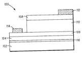
- FIGUREillustrates, schematically, in cross section, a device structure in accordance with the present invention.
- FIGUREillustrates schematically, in cross section, a portion of a microelectronic structure 100 in accordance with an embodiment of the invention.
- Structure 100may be used to form, for example, piezoelectric actuators, piezoelectric transducers, as well as ferroelectric memory cells.
- Microelectronic structure 100includes a monocrystalline silicon substrate 102 , a monocrystalline (Ba,Sr)TiO 3 layer 104 , layers 106 and 108 of conductive, monocrystalline (La,Sr)CoO 3 , a layer 110 of monocrystalline Pb(Mg,Nb) 0 3 —PbTiO 3 , a first electrode 112 , and a second electrode 114 .
- monocrystallineshall have the meaning commonly used within the semiconductor industry.
- structure 100also includes an amorphous intermediate layer 116 positioned between substrate 102 and accommodating buffer layer 104 .
- Substrate 102is preferably a high quality monocrystalline silicon wafer as used in the semiconductor industry.
- Monocrystalline (Ba,Sr)TiO 3 layer 104is preferably a monocrystalline strontium titanate material epitaxially grown on the underlying substrate.
- amorphous intermediate layer 116is grown on substrate 102 at the interface between substrate 102 and the growing (Ba,Sr)TiO 3 layer by the oxidation of substrate 102 during the growth of layer 104 .
- Amorphous interface layer 116is preferably an oxide formed by the oxidation of the surface of substrate 102 , and more preferably is composed of a silicon oxide. Typically, layer 116 has a thickness in the range of approximately 0.5-5 nm.
- (La,Sr)CoO 3 layers 106 and 108are generally configured to allow generation of an electric field across layer 110 . Moreover, monocrystalline layer 106 allows monocrystalline formation of layer 110 over layer 106 .
- layers 106 and 108 compositionis La 0.5 Sr 0.5 CoO 3 . and the layers are preferably greater than 30 nm and more preferably about 30-100 nm thick.
- Monocrystalline piezoelectric layer 110exhibits greater piezoelectric effect compared to polycrystalline films of the same or similar material. Therefore, structures including this monocrystalline film are capable of producing a stronger electronic signal per amount of deformation in the film, and conversely, exhibit greater deformation per amount of electric field applied to the film.
- layer 110is preferably about 30-500 nm thick, and the composition is Pb(Mg 1-x Nb x )O 3 —PbTiO 3 .
- Electrodes 112 and 114facilitate electrical coupling to, respectively, layers 108 and 106 , while providing a relatively inert electrode.
- electrodes 112 and 114are about 100-200 nm thick.
- the crystalline structure of the monocrystalline substrate 102is characterized by a lattice constant and by a lattice orientation.
- layer 110is also a monocrystalline material and the lattice of that monocrystalline material is characterized by a lattice constant and a crystal orientation.
- the lattice constants of layer 110 and the monocrystalline silicon substratemust be closely matched or, alternatively, must be such that upon rotation of one crystal orientation with respect to the other crystal orientation, a substantial match in lattice constants is achieved.
- the terms “substantially equal” and “substantially matched”mean that there is sufficient similarity between the lattice constants to permit the growth of a high quality crystalline layer on the underlying layer.
- substrate 102is a (100) or (111) oriented monocrystalline silicon wafer and substantial matching of lattice constants between the silicon substrate and titanate layer 104 is achieved by rotating the crystal orientation of the titanate material by 45° with respect to the crystal orientation of the silicon substrate wafer.
- Layers 106 - 110are epitaxially grown monocrystalline material and these crystalline materials are also characterized by respective crystal lattice constants and crystal orientations.
- the accommodating buffer layermust be of high crystalline quality.
- substantial matching between the crystal lattice constant of the host crystal, in this case, the monocrystalline (Ba,Sr)TiO 3 , and the grown crystalis desired.
- the following exampleillustrates a process, in accordance the present invention, for fabricating a microelectronic structure such as the structure depicted in the drawing FIGURE.
- the processstarts by providing a monocrystalline semiconductor substrate comprising silicon.
- the semiconductor substrateis a silicon wafer having a (100) orientation.
- the substrateis preferably oriented on axis or, at most, about 0.5° off axis.
- At least a portion of the semiconductor substratehas a bare surface, although other portions of the substrate, as described below, may encompass other structures.
- the term “bare” in this contextmeans that the surface in the portion of the substrate has been cleaned to remove any oxides, contaminants, or other foreign material.
- bare siliconis highly reactive and readily forms a native oxide.
- the term “bare”is intended to encompass such a native oxide.
- a thin silicon oxidemay also be intentionally grown on the semiconductor substrate, although such a grown oxide is not essential to the process in accordance with the invention.
- the native oxide layerIn order to epitaxially grow a monocrystalline (Ba,Sr)TiO 3 layer overlying the monocrystalline silicon substrate, the native oxide layer must first be removed to expose the crystalline structure of the underlying substrate. The following process is preferably carried out by molecular beam epitaxy (MBE), although other epitaxial processes may also be used in accordance with the present invention.
- MBEmolecular beam epitaxy
- the native oxidecan be removed by first thermally depositing a thin layer of strontium, barium, or a combination of strontium and barium in an MBE apparatus.
- the substrateis then heated to a temperature of about 750° C. to cause the strontium to react with the native silicon oxide layer.
- the strontiumserves to reduce the silicon oxide to leave a silicon oxide-free surface.
- the resultant surfacewhich exhibits an ordered 2 ⁇ 1 structure, includes strontium, oxygen, and silicon.
- the ordered 2 ⁇ 1 structureforms a template for the ordered growth of an overlying titanate layer.
- the templateprovides the necessary chemical and physical properties to nucleate the crystalline growth of an overlying layer.
- the native silicon oxidecan be converted and the substrate surface can be prepared for the growth of a monocrystalline oxide layer by depositing strontium oxide, strontium barium oxide, or barium oxide, onto the substrate surface by MBE at a low temperature and by subsequently heating the structure to a temperature of about 750° C. At this temperature, a solid state reaction takes place between the strontium oxide and the native silicon oxide, causing the reduction of the native silicon oxide and leaving an ordered 2 ⁇ 1 structure with strontium, oxygen, and silicon remaining on the substrate surface. Again, this forms a template for the subsequent growth of an ordered monocrystalline titanate layer.
- the substrateis cooled to a temperature in the range of about 200-800° C. and a layer (e.g., about 9-11 nm)of strontium titanate is grown on the template layer by molecular beam epitaxy.
- the MBE processis initiated by opening shutters in the MBE apparatus to expose strontium, titanium and oxygen sources.
- the ratio of strontium and titaniumis approximately 1:1.
- the partial pressure of oxygenis initially set at a minimum value to grow stochiometric strontium titanate at a growth rate of about 0.3-0.5 nm per minute. After initiating growth of the strontium titanate, the partial pressure of oxygen is increased above the initial minimum value.
- the overpressure of oxygencauses the growth of an amorphous silicon oxide layer at the interface between the underlying substrate and the growing strontium titanate layer.
- the growth of the silicon oxide layerresults from the diffusion of oxygen through the growing strontium titanate layer to the interface where the oxygen reacts with silicon at the surface of the underlying substrate.
- the strontium titanategrows as an ordered monocrystal with the crystalline orientation rotated by 45° with respect to the ordered 2 ⁇ 1 crystalline structure of the underlying substrate.
- the monocrystalline strontium titanatemay be capped by a template layer that is conducive to the subsequent growth of an epitaxial layer of a desired piezoelectric material.
- the MBE growth of the strontium titanate monocrystalline layercan be capped by terminating the growth with 1-2 monolayers of titanium, 1-2 monolayers of titanium-oxygen or with 1-2 monolayers of strontium-oxygen.
- the (La,Sr)CoO 3 materialis grown using sputter deposition. More particularly, the (La,Sr)CoO 3 layer is grown by RF magnetron sputtering (face to face configuration) from a compressed (La,Sr)CoO 3 target. The deposition is performed with oxygen as sputter gas, and a substrate temperature of about 400-600° C.
- layer 110is formed over (La,Sr)CoO 3 layer 106 using a spin-on, sol-gel coating technique, then calcined and crystallized between 350° C. and 800° C. to form a monocrystalline layer.
- Layer 110may also be formed using PVD or CVD techniques.
- Electrodes 112 and 114are subsequently formed over monocrystalline layers 106 and 108 using sputter deposition techniques to deposit the electrode material (e.g., platinum or iridium) and subsequently patterning and etching the material to remove the material from a portion of layers 106 and 108 .
- the electrode materiale.g., platinum or iridium
- platinummay be deposited over (La,Sr)CoO 3 layers 106 and 108 by sputtering material from a platinum target onto the (La,Sr)CoO 3 layer using RF magnetron sputtering in an inert environment. After the platinum is deposited, the platinum may be photolithographically patterned and etched using a suitable wet or dry etch environment to form electrode 112 and 114 .
Landscapes
- Engineering & Computer Science (AREA)
- Manufacturing & Machinery (AREA)
- Microelectronics & Electronic Packaging (AREA)
- General Physics & Mathematics (AREA)
- Condensed Matter Physics & Semiconductors (AREA)
- Computer Hardware Design (AREA)
- Physics & Mathematics (AREA)
- Power Engineering (AREA)
- Chemical & Material Sciences (AREA)
- Materials Engineering (AREA)
- Dispersion Chemistry (AREA)
- Physical Vapour Deposition (AREA)
- Crystals, And After-Treatments Of Crystals (AREA)
- Semiconductor Memories (AREA)
Abstract
Description
- This invention relates generally to microelectronic structures and devices and to a method for their fabrication, and more specifically to structures and devices including piezoelectric thin films and to the fabrication and use of the structures and devices.[0001]
- Piezoelectric materials are useful for a variety of applications. For example, piezoelectric material is often used to form pressure gauges, transducers, tactile sensors, robotic manipulator, high frequency sound generators, frequency control circuits, and oscillators.[0002]
- Generally, the desirable characteristic of the piezoelectric material, i.e., the piezoelectric effect, increases as the crystallinity of the material increases. Accordingly piezoelectric material of high crystalline quality if often desired.[0003]
- Piezoelectric material is relatively expensive in bulk form compared to other materials used to form microelectronic devices such as microelectronic pressure sensors, oscillators, and the like. Because of their present generally high cost and low availability in bulk form, for many years attempts have been made to grow thin films of the piezoelectric materials on a foreign substrate. To achieve optimal characteristics of piezoelectric material, however, a monocrystalline film of high crystalline quality is desired. Attempts have been made, for example, to grow layers of a monocrystalline piezoelectric material on substrates such as silicon. These attempts have generally been unsuccessful because lattice mismatches between the host crystal and the grown crystal have caused the resulting thin film of piezoelectric material to be of low crystalline quality.[0004]
- If a large area thin film of high quality monocrystalline piezoelectric material was available at low cost, a variety of semiconductor microelectronic devices could advantageously be fabricated using that film at a low cost compared to the cost of fabricating such devices on a bulk wafer of the piezoelectric material. In addition, if a thin film of high quality monocrystalline piezoelectric material could be realized on a bulk wafer such as a silicon wafer, an integrated device structure could be achieved that took advantage of the best properties of both the silicon and the piezoelectric material.[0005]
- Accordingly, a need exists for a microelectronic structure that provides a high quality monocrystalline piezoelectric film over another monocrystalline material and for a process for making such a structure.[0006]
- The present invention is illustrated by way of example and not limitation in the accompanying FIGURE, which illustrates, schematically, in cross section, a device structure in accordance with the present invention.[0007]
- The drawing FIGURE illustrates schematically, in cross section, a portion of a[0008]
microelectronic structure 100 in accordance with an embodiment of the invention.Structure 100 may be used to form, for example, piezoelectric actuators, piezoelectric transducers, as well as ferroelectric memory cells. - [0009]
Microelectronic structure 100 includes amonocrystalline silicon substrate 102, a monocrystalline (Ba,Sr)TiO3layer104,layers layer 110 of monocrystalline Pb(Mg,Nb)03—PbTiO3, afirst electrode 112, and asecond electrode 114. As used throughout this document, the term “monocrystalline” shall have the meaning commonly used within the semiconductor industry. The term shall refer to materials that are a single crystal or that are substantially a single crystal and shall include those materials having a relatively small number of defects such as dislocations and the like as are commonly found in substrates of silicon or germanium or mixtures of silicon and germanium and epitaxial layers of such materials commonly found in the semiconductor industry. In accordance with the invention,structure 100 also includes an amorphousintermediate layer 116 positioned betweensubstrate 102 and accommodatingbuffer layer 104. - [0010]
Substrate 102, in accordance with an embodiment of the invention, is preferably a high quality monocrystalline silicon wafer as used in the semiconductor industry. Monocrystalline (Ba,Sr)TiO3layer104 is preferably a monocrystalline strontium titanate material epitaxially grown on the underlying substrate. In accordance with one embodiment of the invention, amorphousintermediate layer 116 is grown onsubstrate 102 at the interface betweensubstrate 102 and the growing (Ba,Sr)TiO3layer by the oxidation ofsubstrate 102 during the growth oflayer 104. - [0011]
Amorphous interface layer 116 is preferably an oxide formed by the oxidation of the surface ofsubstrate 102, and more preferably is composed of a silicon oxide. Typically,layer 116 has a thickness in the range of approximately 0.5-5 nm. - (La,Sr)CoO[0012]3layers106 and108 are generally configured to allow generation of an electric field across
layer 110. Moreover,monocrystalline layer 106 allows monocrystalline formation oflayer 110 overlayer 106. In accordance with a preferred embodiment of the invention,layers - Monocrystalline[0013]
piezoelectric layer 110 exhibits greater piezoelectric effect compared to polycrystalline films of the same or similar material. Therefore, structures including this monocrystalline film are capable of producing a stronger electronic signal per amount of deformation in the film, and conversely, exhibit greater deformation per amount of electric field applied to the film. To provide the desired piezoelectric effect,layer 110 is preferably about 30-500 nm thick, and the composition is Pb(Mg1-xNbx)O3—PbTiO3. - [0014]
Electrodes layers electrodes - The crystalline structure of the[0015]
monocrystalline substrate 102 is characterized by a lattice constant and by a lattice orientation. In a similar manner,layer 110 is also a monocrystalline material and the lattice of that monocrystalline material is characterized by a lattice constant and a crystal orientation. The lattice constants oflayer 110 and the monocrystalline silicon substrate must be closely matched or, alternatively, must be such that upon rotation of one crystal orientation with respect to the other crystal orientation, a substantial match in lattice constants is achieved. In this context the terms “substantially equal” and “substantially matched” mean that there is sufficient similarity between the lattice constants to permit the growth of a high quality crystalline layer on the underlying layer. - In accordance with one embodiment of the invention,[0016]
substrate 102 is a (100) or (111) oriented monocrystalline silicon wafer and substantial matching of lattice constants between the silicon substrate andtitanate layer 104 is achieved by rotating the crystal orientation of the titanate material by 45° with respect to the crystal orientation of the silicon substrate wafer. - Layers[0017]106-110 are epitaxially grown monocrystalline material and these crystalline materials are also characterized by respective crystal lattice constants and crystal orientations. To achieve high crystalline quality in these epitaxially grown monocrystalline layers, the accommodating buffer layer must be of high crystalline quality. In addition, in order to achieve high crystalline quality in subsequently deposited films106-110, substantial matching between the crystal lattice constant of the host crystal, in this case, the monocrystalline (Ba,Sr)TiO3, and the grown crystal is desired.
- The following example illustrates a process, in accordance the present invention, for fabricating a microelectronic structure such as the structure depicted in the drawing FIGURE. The process starts by providing a monocrystalline semiconductor substrate comprising silicon. In accordance with a preferred embodiment of the invention, the semiconductor substrate is a silicon wafer having a (100) orientation. The substrate is preferably oriented on axis or, at most, about 0.5° off axis. At least a portion of the semiconductor substrate has a bare surface, although other portions of the substrate, as described below, may encompass other structures. The term “bare” in this context means that the surface in the portion of the substrate has been cleaned to remove any oxides, contaminants, or other foreign material. As is well known, bare silicon is highly reactive and readily forms a native oxide. The term “bare” is intended to encompass such a native oxide. A thin silicon oxide may also be intentionally grown on the semiconductor substrate, although such a grown oxide is not essential to the process in accordance with the invention. In order to epitaxially grow a monocrystalline (Ba,Sr)TiO[0018]3layer overlying the monocrystalline silicon substrate, the native oxide layer must first be removed to expose the crystalline structure of the underlying substrate. The following process is preferably carried out by molecular beam epitaxy (MBE), although other epitaxial processes may also be used in accordance with the present invention. The native oxide can be removed by first thermally depositing a thin layer of strontium, barium, or a combination of strontium and barium in an MBE apparatus. In the case where strontium is used, the substrate is then heated to a temperature of about 750° C. to cause the strontium to react with the native silicon oxide layer. The strontium serves to reduce the silicon oxide to leave a silicon oxide-free surface. The resultant surface, which exhibits an ordered 2×1 structure, includes strontium, oxygen, and silicon. The ordered 2×1 structure forms a template for the ordered growth of an overlying titanate layer. The template provides the necessary chemical and physical properties to nucleate the crystalline growth of an overlying layer.
- In accordance with an alternate embodiment of the invention, the native silicon oxide can be converted and the substrate surface can be prepared for the growth of a monocrystalline oxide layer by depositing strontium oxide, strontium barium oxide, or barium oxide, onto the substrate surface by MBE at a low temperature and by subsequently heating the structure to a temperature of about 750° C. At this temperature, a solid state reaction takes place between the strontium oxide and the native silicon oxide, causing the reduction of the native silicon oxide and leaving an ordered 2×1 structure with strontium, oxygen, and silicon remaining on the substrate surface. Again, this forms a template for the subsequent growth of an ordered monocrystalline titanate layer.[0019]
- Following the removal of the silicon oxide from the surface of the substrate, in accordance with one embodiment of the invention, the substrate is cooled to a temperature in the range of about 200-800° C. and a layer (e.g., about 9-11 nm)of strontium titanate is grown on the template layer by molecular beam epitaxy. The MBE process is initiated by opening shutters in the MBE apparatus to expose strontium, titanium and oxygen sources. The ratio of strontium and titanium is approximately 1:1. The partial pressure of oxygen is initially set at a minimum value to grow stochiometric strontium titanate at a growth rate of about 0.3-0.5 nm per minute. After initiating growth of the strontium titanate, the partial pressure of oxygen is increased above the initial minimum value. The overpressure of oxygen causes the growth of an amorphous silicon oxide layer at the interface between the underlying substrate and the growing strontium titanate layer. The growth of the silicon oxide layer results from the diffusion of oxygen through the growing strontium titanate layer to the interface where the oxygen reacts with silicon at the surface of the underlying substrate. The strontium titanate grows as an ordered monocrystal with the crystalline orientation rotated by 45° with respect to the ordered 2×1 crystalline structure of the underlying substrate.[0020]
- After the strontium titanate layer has been grown to the desired thickness, the monocrystalline strontium titanate may be capped by a template layer that is conducive to the subsequent growth of an epitaxial layer of a desired piezoelectric material. For example, the MBE growth of the strontium titanate monocrystalline layer can be capped by terminating the growth with 1-2 monolayers of titanium, 1-2 monolayers of titanium-oxygen or with 1-2 monolayers of strontium-oxygen.[0021]
- Following the formation of the template (or, if no template is formed, after formation of the titanate layer), the (La,Sr)CoO[0022]3material is grown using sputter deposition. More particularly, the (La,Sr)CoO3layer is grown by RF magnetron sputtering (face to face configuration) from a compressed (La,Sr)CoO3target. The deposition is performed with oxygen as sputter gas, and a substrate temperature of about 400-600° C.
- Next,[0023]
layer 110 is formed over (La,Sr)CoO3layer106 using a spin-on, sol-gel coating technique, then calcined and crystallized between 350° C. and 800° C. to form a monocrystalline layer.Layer 110 may also be formed using PVD or CVD techniques. - [0024]
Electrodes monocrystalline layers layers electrode - In the foregoing specification, the invention has been described with reference to specific embodiments. However, one of ordinary skill in the art appreciates that various modifications and changes can be made without departing from the scope of the present invention as set forth in the claims below. Accordingly, the specification and FIGURE are to be regarded in an illustrative rather than a restrictive sense, and all such modifications are intended to be included within the scope of present invention.[0025]
- Benefits, other advantages, and solutions to problems have been described above with regard to specific embodiments. However, the benefits, advantages, solutions to problems, and any element(s) that may cause any benefit, advantage, or solution to occur or become more pronounced are not to be construed as a critical, required, or essential features or elements of any or all the claims. As used herein, the terms “comprises,” “comprising,” or any other variation thereof, are intended to cover a non-exclusive inclusion, such that a process, method, article, or apparatus that comprises a list of elements does not include only those elements but may include other elements not expressly listed or inherent to such process, method, article, or apparatus.[0026]
Claims (25)
Priority Applications (2)
| Application Number | Priority Date | Filing Date | Title |
|---|---|---|---|
| US09/912,994US6482538B2 (en) | 2000-07-24 | 2001-07-25 | Microelectronic piezoelectric structure and method of forming the same |
| PCT/US2002/020214WO2003010834A2 (en) | 2001-07-25 | 2002-06-26 | Microelectronic piezoelectric structure |
Applications Claiming Priority (2)
| Application Number | Priority Date | Filing Date | Title |
|---|---|---|---|
| US09/624,527US6432546B1 (en) | 2000-07-24 | 2000-07-24 | Microelectronic piezoelectric structure and method of forming the same |
| US09/912,994US6482538B2 (en) | 2000-07-24 | 2001-07-25 | Microelectronic piezoelectric structure and method of forming the same |
Related Parent Applications (1)
| Application Number | Title | Priority Date | Filing Date |
|---|---|---|---|
| US09/624,527Continuation-In-PartUS6432546B1 (en) | 2000-07-24 | 2000-07-24 | Microelectronic piezoelectric structure and method of forming the same |
Publications (2)
| Publication Number | Publication Date |
|---|---|
| US20020009612A1true US20020009612A1 (en) | 2002-01-24 |
| US6482538B2 US6482538B2 (en) | 2002-11-19 |
Family
ID=25432824
Family Applications (1)
| Application Number | Title | Priority Date | Filing Date |
|---|---|---|---|
| US09/912,994Expired - Fee RelatedUS6482538B2 (en) | 2000-07-24 | 2001-07-25 | Microelectronic piezoelectric structure and method of forming the same |
Country Status (2)
| Country | Link |
|---|---|
| US (1) | US6482538B2 (en) |
| WO (1) | WO2003010834A2 (en) |
Cited By (6)
| Publication number | Priority date | Publication date | Assignee | Title |
|---|---|---|---|---|
| US20040214352A1 (en)* | 2002-10-24 | 2004-10-28 | Seiko Epson Corporation | Ferroelectric film, ferroelectric capacitor, ferroelectric memory, piezoelectric element, semiconductor element, method of manufacturing ferroelectric film, and method of manufacturing ferroelectric capacitor |
| US20060288928A1 (en)* | 2005-06-10 | 2006-12-28 | Chang-Beom Eom | Perovskite-based thin film structures on miscut semiconductor substrates |
| WO2009043639A1 (en)* | 2007-09-29 | 2009-04-09 | Universite De Liege | Material comprising finely layered heterostructures of oxide materials |
| US20150177458A1 (en)* | 2013-12-20 | 2015-06-25 | The Regents Of The University Of California | Bonding of heterogeneous material grown on silicon to a silicon photonic circuit |
| US20160124145A1 (en)* | 2014-10-29 | 2016-05-05 | Commissariat A L'energie Atomique Et Aux Energies Alternatives | Prestructured substrate for the production of photonic components, associated photonic circuit and manufacturing method |
| US10852492B1 (en)* | 2014-10-29 | 2020-12-01 | Acacia Communications, Inc. | Techniques to combine two integrated photonic substrates |
Families Citing this family (2)
| Publication number | Priority date | Publication date | Assignee | Title |
|---|---|---|---|---|
| JP2016032007A (en)* | 2014-07-28 | 2016-03-07 | 株式会社リコー | Method for manufacturing piezoelectric film, method for manufacturing piezoelectric element, liquid discharge head and imaging apparatus |
| KR20210149162A (en) | 2019-04-08 | 2021-12-08 | 케플러 컴퓨팅 인크. | Doped polar layer and semiconductor device comprising same |
Citations (1)
| Publication number | Priority date | Publication date | Assignee | Title |
|---|---|---|---|---|
| US5248564A (en)* | 1992-12-09 | 1993-09-28 | Bell Communications Research, Inc. | C-axis perovskite thin films grown on silicon dioxide |
Family Cites Families (17)
| Publication number | Priority date | Publication date | Assignee | Title |
|---|---|---|---|---|
| JPH0695554B2 (en) | 1987-10-12 | 1994-11-24 | 工業技術院長 | Method for forming single crystal magnesia spinel film |
| US4999842A (en) | 1989-03-01 | 1991-03-12 | At&T Bell Laboratories | Quantum well vertical cavity laser |
| US5310707A (en) | 1990-03-28 | 1994-05-10 | Superconductivity Research Laboratory International | Substrate material for the preparation of oxide superconductors |
| US5270298A (en) | 1992-03-05 | 1993-12-14 | Bell Communications Research, Inc. | Cubic metal oxide thin film epitaxially grown on silicon |
| US5155658A (en) | 1992-03-05 | 1992-10-13 | Bell Communications Research, Inc. | Crystallographically aligned ferroelectric films usable in memories and method of crystallographically aligning perovskite films |
| US5326721A (en) | 1992-05-01 | 1994-07-05 | Texas Instruments Incorporated | Method of fabricating high-dielectric constant oxides on semiconductors using a GE buffer layer |
| JPH06151872A (en) | 1992-11-09 | 1994-05-31 | Mitsubishi Kasei Corp | Fet device |
| EP0600303B1 (en) | 1992-12-01 | 2002-02-06 | Matsushita Electric Industrial Co., Ltd. | Method for fabrication of dielectric thin film |
| US5828080A (en) | 1994-08-17 | 1998-10-27 | Tdk Corporation | Oxide thin film, electronic device substrate and electronic device |
| US5635741A (en) | 1994-09-30 | 1997-06-03 | Texas Instruments Incorporated | Barium strontium titanate (BST) thin films by erbium donor doping |
| US5479317A (en)* | 1994-10-05 | 1995-12-26 | Bell Communications Research, Inc. | Ferroelectric capacitor heterostructure and method of making same |
| US5753934A (en) | 1995-08-04 | 1998-05-19 | Tok Corporation | Multilayer thin film, substrate for electronic device, electronic device, and preparation of multilayer oxide thin film |
| FR2744578B1 (en) | 1996-02-06 | 1998-04-30 | Motorola Semiconducteurs | HIGH FREQUENCY AMPLIFIER |
| US5912068A (en)* | 1996-12-05 | 1999-06-15 | The Regents Of The University Of California | Epitaxial oxides on amorphous SiO2 on single crystal silicon |
| US6002375A (en) | 1997-09-02 | 1999-12-14 | Motorola, Inc. | Multi-substrate radio-frequency circuit |
| US6055179A (en) | 1998-05-19 | 2000-04-25 | Canon Kk | Memory device utilizing giant magnetoresistance effect |
| US6432546B1 (en)* | 2000-07-24 | 2002-08-13 | Motorola, Inc. | Microelectronic piezoelectric structure and method of forming the same |
- 2001
- 2001-07-25USUS09/912,994patent/US6482538B2/ennot_activeExpired - Fee Related
- 2002
- 2002-06-26WOPCT/US2002/020214patent/WO2003010834A2/ennot_activeApplication Discontinuation
Patent Citations (1)
| Publication number | Priority date | Publication date | Assignee | Title |
|---|---|---|---|---|
| US5248564A (en)* | 1992-12-09 | 1993-09-28 | Bell Communications Research, Inc. | C-axis perovskite thin films grown on silicon dioxide |
Cited By (10)
| Publication number | Priority date | Publication date | Assignee | Title |
|---|---|---|---|---|
| US20040214352A1 (en)* | 2002-10-24 | 2004-10-28 | Seiko Epson Corporation | Ferroelectric film, ferroelectric capacitor, ferroelectric memory, piezoelectric element, semiconductor element, method of manufacturing ferroelectric film, and method of manufacturing ferroelectric capacitor |
| US7255941B2 (en)* | 2002-10-24 | 2007-08-14 | Seiko Epson Corporation | Ferroelectric film, ferroelectric capacitor, ferroelectric memory, piezoelectric element, semiconductor element, method of manufacturing ferroelectric film, and method of manufacturing ferroelectric capacitor |
| US20060288928A1 (en)* | 2005-06-10 | 2006-12-28 | Chang-Beom Eom | Perovskite-based thin film structures on miscut semiconductor substrates |
| WO2009043639A1 (en)* | 2007-09-29 | 2009-04-09 | Universite De Liege | Material comprising finely layered heterostructures of oxide materials |
| US20150177458A1 (en)* | 2013-12-20 | 2015-06-25 | The Regents Of The University Of California | Bonding of heterogeneous material grown on silicon to a silicon photonic circuit |
| US9360623B2 (en)* | 2013-12-20 | 2016-06-07 | The Regents Of The University Of California | Bonding of heterogeneous material grown on silicon to a silicon photonic circuit |
| US20160124145A1 (en)* | 2014-10-29 | 2016-05-05 | Commissariat A L'energie Atomique Et Aux Energies Alternatives | Prestructured substrate for the production of photonic components, associated photonic circuit and manufacturing method |
| US10267989B2 (en)* | 2014-10-29 | 2019-04-23 | Commissariat à l'énergie atomique et aux énergies alternatives | Prestructured substrate for the production of photonic components, associated photonic circuit and manufacturing method |
| US10852492B1 (en)* | 2014-10-29 | 2020-12-01 | Acacia Communications, Inc. | Techniques to combine two integrated photonic substrates |
| US11409059B1 (en) | 2014-10-29 | 2022-08-09 | Acacia Communications, Inc. | Techniques to combine two integrated photonic substrates |
Also Published As
| Publication number | Publication date |
|---|---|
| WO2003010834A3 (en) | 2003-07-24 |
| WO2003010834A2 (en) | 2003-02-06 |
| US6482538B2 (en) | 2002-11-19 |
Similar Documents
| Publication | Publication Date | Title |
|---|---|---|
| US6432546B1 (en) | Microelectronic piezoelectric structure and method of forming the same | |
| US7020374B2 (en) | Optical waveguide structure and method for fabricating the same | |
| US6563118B2 (en) | Pyroelectric device on a monocrystalline semiconductor substrate and process for fabricating same | |
| US6555946B1 (en) | Acoustic wave device and process for forming the same | |
| US6709776B2 (en) | Multilayer thin film and its fabrication process as well as electron device | |
| JP2000067650A (en) | Ferroelectric thin film element and method of manufacturing the same | |
| US20020006733A1 (en) | Multilayer thin film and its fabrication process as well as electron device | |
| KR20050083598A (en) | Thin film multilayer body, electronic device using such thin film multilayer body, actuator, and method for manufacturing actuator | |
| US6693298B2 (en) | Structure and method for fabricating epitaxial semiconductor on insulator (SOI) structures and devices utilizing the formation of a compliant substrate for materials used to form same | |
| US6482538B2 (en) | Microelectronic piezoelectric structure and method of forming the same | |
| JP4427925B2 (en) | Laminated thin film manufacturing method and electronic device | |
| WO2002009159A2 (en) | Thin-film metallic oxide structure and process for fabricating same | |
| WO2002009158A2 (en) | Semiconductor structure including a magnetic tunnel junction | |
| WO2002009191A2 (en) | Non-volatile memory element | |
| JP2889492B2 (en) | Preparation method of oxide thin film | |
| US20020003238A1 (en) | Structure including cubic boron nitride films and method of forming the same | |
| JP2889463B2 (en) | Oriented ferroelectric thin film device | |
| KR100485409B1 (en) | Stratified structure with a ferroelectric layer and process for producing the same | |
| JPH10275896A (en) | Memory element | |
| JPH05234419A (en) | Device using dielectric | |
| CN119384212A (en) | Semiconductor structure and manufacturing method thereof, and electronic device | |
| US20020136931A1 (en) | Acousto-optic structure, device including the structure, and methods of forming the device and structure | |
| JPH11103027A (en) | Manufacturing ferroelectric film and ferroelectric thin film elements, ferroelectric thin film structure and ferroelectric thin film element |
Legal Events
| Date | Code | Title | Description |
|---|---|---|---|
| AS | Assignment | Owner name:MOTOROLA, INC., ILLINOIS Free format text:ASSIGNMENT OF ASSIGNORS INTEREST;ASSIGNORS:RAMESH, RAMAMOORTHY;WANG, YU;FINDER, JEFFREY M.;AND OTHERS;REEL/FRAME:012045/0895;SIGNING DATES FROM 20010709 TO 20010717 | |
| AS | Assignment | Owner name:FREESCALE SEMICONDUCTOR, INC., TEXAS Free format text:ASSIGNMENT OF ASSIGNORS INTEREST;ASSIGNOR:MOTOROLA, INC.;REEL/FRAME:015698/0657 Effective date:20040404 Owner name:FREESCALE SEMICONDUCTOR, INC.,TEXAS Free format text:ASSIGNMENT OF ASSIGNORS INTEREST;ASSIGNOR:MOTOROLA, INC.;REEL/FRAME:015698/0657 Effective date:20040404 | |
| FPAY | Fee payment | Year of fee payment:4 | |
| AS | Assignment | Owner name:CITIBANK, N.A. AS COLLATERAL AGENT, NEW YORK Free format text:SECURITY AGREEMENT;ASSIGNORS:FREESCALE SEMICONDUCTOR, INC.;FREESCALE ACQUISITION CORPORATION;FREESCALE ACQUISITION HOLDINGS CORP.;AND OTHERS;REEL/FRAME:018855/0129 Effective date:20061201 Owner name:CITIBANK, N.A. AS COLLATERAL AGENT,NEW YORK Free format text:SECURITY AGREEMENT;ASSIGNORS:FREESCALE SEMICONDUCTOR, INC.;FREESCALE ACQUISITION CORPORATION;FREESCALE ACQUISITION HOLDINGS CORP.;AND OTHERS;REEL/FRAME:018855/0129 Effective date:20061201 | |
| AS | Assignment | Owner name:UNIVERSITY OF MARYLAND, MARYLAND Free format text:ASSIGNMENT OF ASSIGNORS INTEREST;ASSIGNORS:RAMESH, RAMAMOORTHY;WANG, YU;FINDER, JEFFREY M.;AND OTHERS;REEL/FRAME:019569/0883;SIGNING DATES FROM 20010709 TO 20010717 | |
| FPAY | Fee payment | Year of fee payment:8 | |
| AS | Assignment | Owner name:CITIBANK, N.A., AS COLLATERAL AGENT,NEW YORK Free format text:SECURITY AGREEMENT;ASSIGNOR:FREESCALE SEMICONDUCTOR, INC.;REEL/FRAME:024397/0001 Effective date:20100413 Owner name:CITIBANK, N.A., AS COLLATERAL AGENT, NEW YORK Free format text:SECURITY AGREEMENT;ASSIGNOR:FREESCALE SEMICONDUCTOR, INC.;REEL/FRAME:024397/0001 Effective date:20100413 | |
| AS | Assignment | Owner name:CITIBANK, N.A., AS NOTES COLLATERAL AGENT, NEW YORK Free format text:SECURITY AGREEMENT;ASSIGNOR:FREESCALE SEMICONDUCTOR, INC.;REEL/FRAME:030633/0424 Effective date:20130521 Owner name:CITIBANK, N.A., AS NOTES COLLATERAL AGENT, NEW YOR Free format text:SECURITY AGREEMENT;ASSIGNOR:FREESCALE SEMICONDUCTOR, INC.;REEL/FRAME:030633/0424 Effective date:20130521 | |
| AS | Assignment | Owner name:CITIBANK, N.A., AS NOTES COLLATERAL AGENT, NEW YORK Free format text:SECURITY AGREEMENT;ASSIGNOR:FREESCALE SEMICONDUCTOR, INC.;REEL/FRAME:031591/0266 Effective date:20131101 Owner name:CITIBANK, N.A., AS NOTES COLLATERAL AGENT, NEW YOR Free format text:SECURITY AGREEMENT;ASSIGNOR:FREESCALE SEMICONDUCTOR, INC.;REEL/FRAME:031591/0266 Effective date:20131101 | |
| REMI | Maintenance fee reminder mailed | ||
| LAPS | Lapse for failure to pay maintenance fees | ||
| STCH | Information on status: patent discontinuation | Free format text:PATENT EXPIRED DUE TO NONPAYMENT OF MAINTENANCE FEES UNDER 37 CFR 1.362 | |
| FP | Lapsed due to failure to pay maintenance fee | Effective date:20141119 | |
| AS | Assignment | Owner name:FREESCALE SEMICONDUCTOR, INC., TEXAS Free format text:PATENT RELEASE;ASSIGNOR:CITIBANK, N.A., AS COLLATERAL AGENT;REEL/FRAME:037354/0225 Effective date:20151207 Owner name:FREESCALE SEMICONDUCTOR, INC., TEXAS Free format text:PATENT RELEASE;ASSIGNOR:CITIBANK, N.A., AS COLLATERAL AGENT;REEL/FRAME:037356/0143 Effective date:20151207 Owner name:FREESCALE SEMICONDUCTOR, INC., TEXAS Free format text:PATENT RELEASE;ASSIGNOR:CITIBANK, N.A., AS COLLATERAL AGENT;REEL/FRAME:037356/0553 Effective date:20151207 | |
| AS | Assignment | Owner name:MORGAN STANLEY SENIOR FUNDING, INC., MARYLAND Free format text:ASSIGNMENT AND ASSUMPTION OF SECURITY INTEREST IN PATENTS;ASSIGNOR:CITIBANK, N.A.;REEL/FRAME:037486/0517 Effective date:20151207 | |
| AS | Assignment | Owner name:MORGAN STANLEY SENIOR FUNDING, INC., MARYLAND Free format text:ASSIGNMENT AND ASSUMPTION OF SECURITY INTEREST IN PATENTS;ASSIGNOR:CITIBANK, N.A.;REEL/FRAME:037518/0292 Effective date:20151207 | |
| AS | Assignment | Owner name:NXP, B.V., F/K/A FREESCALE SEMICONDUCTOR, INC., NETHERLANDS Free format text:RELEASE BY SECURED PARTY;ASSIGNOR:MORGAN STANLEY SENIOR FUNDING, INC.;REEL/FRAME:040925/0001 Effective date:20160912 Owner name:NXP, B.V., F/K/A FREESCALE SEMICONDUCTOR, INC., NE Free format text:RELEASE BY SECURED PARTY;ASSIGNOR:MORGAN STANLEY SENIOR FUNDING, INC.;REEL/FRAME:040925/0001 Effective date:20160912 | |
| AS | Assignment | Owner name:NXP B.V., NETHERLANDS Free format text:RELEASE BY SECURED PARTY;ASSIGNOR:MORGAN STANLEY SENIOR FUNDING, INC.;REEL/FRAME:040928/0001 Effective date:20160622 | |
| AS | Assignment | Owner name:MORGAN STANLEY SENIOR FUNDING, INC., MARYLAND Free format text:CORRECTIVE ASSIGNMENT TO CORRECT THE REMOVE PATENTS 8108266 AND 8062324 AND REPLACE THEM WITH 6108266 AND 8060324 PREVIOUSLY RECORDED ON REEL 037518 FRAME 0292. ASSIGNOR(S) HEREBY CONFIRMS THE ASSIGNMENT AND ASSUMPTION OF SECURITY INTEREST IN PATENTS;ASSIGNOR:CITIBANK, N.A.;REEL/FRAME:041703/0536 Effective date:20151207 | |
| AS | Assignment | Owner name:SHENZHEN XINGUODU TECHNOLOGY CO., LTD., CHINA Free format text:CORRECTIVE ASSIGNMENT TO CORRECT THE TO CORRECT THE APPLICATION NO. FROM 13,883,290 TO 13,833,290 PREVIOUSLY RECORDED ON REEL 041703 FRAME 0536. ASSIGNOR(S) HEREBY CONFIRMS THE THE ASSIGNMENT AND ASSUMPTION OF SECURITYINTEREST IN PATENTS.;ASSIGNOR:MORGAN STANLEY SENIOR FUNDING, INC.;REEL/FRAME:048734/0001 Effective date:20190217 | |
| AS | Assignment | Owner name:MORGAN STANLEY SENIOR FUNDING, INC., MARYLAND Free format text:CORRECTIVE ASSIGNMENT TO CORRECT THE REMOVE APPLICATION11759915 AND REPLACE IT WITH APPLICATION 11759935 PREVIOUSLY RECORDED ON REEL 037486 FRAME 0517. ASSIGNOR(S) HEREBY CONFIRMS THE ASSIGNMENT AND ASSUMPTION OF SECURITYINTEREST IN PATENTS;ASSIGNOR:CITIBANK, N.A.;REEL/FRAME:053547/0421 Effective date:20151207 | |
| AS | Assignment | Owner name:NXP B.V., NETHERLANDS Free format text:CORRECTIVE ASSIGNMENT TO CORRECT THE REMOVEAPPLICATION 11759915 AND REPLACE IT WITH APPLICATION11759935 PREVIOUSLY RECORDED ON REEL 040928 FRAME 0001. ASSIGNOR(S) HEREBY CONFIRMS THE RELEASE OF SECURITYINTEREST;ASSIGNOR:MORGAN STANLEY SENIOR FUNDING, INC.;REEL/FRAME:052915/0001 Effective date:20160622 | |
| AS | Assignment | Owner name:NXP, B.V. F/K/A FREESCALE SEMICONDUCTOR, INC., NETHERLANDS Free format text:CORRECTIVE ASSIGNMENT TO CORRECT THE REMOVEAPPLICATION 11759915 AND REPLACE IT WITH APPLICATION11759935 PREVIOUSLY RECORDED ON REEL 040925 FRAME 0001. ASSIGNOR(S) HEREBY CONFIRMS THE RELEASE OF SECURITYINTEREST;ASSIGNOR:MORGAN STANLEY SENIOR FUNDING, INC.;REEL/FRAME:052917/0001 Effective date:20160912 |