US20020009277A1 - Waveguides and wavelength demultiplexers in two-dimensional photonic crystal slabs - Google Patents
Waveguides and wavelength demultiplexers in two-dimensional photonic crystal slabsDownload PDFInfo
- Publication number
- US20020009277A1 US20020009277A1US09/814,728US81472801AUS2002009277A1US 20020009277 A1US20020009277 A1US 20020009277A1US 81472801 AUS81472801 AUS 81472801AUS 2002009277 A1US2002009277 A1US 2002009277A1
- Authority
- US
- United States
- Prior art keywords
- photonic crystal
- waveguide
- light
- electromagnetic radiation
- refractive index
- Prior art date
- Legal status (The legal status is an assumption and is not a legal conclusion. Google has not performed a legal analysis and makes no representation as to the accuracy of the status listed.)
- Granted
Links
Images


Classifications
- G—PHYSICS
- G02—OPTICS
- G02B—OPTICAL ELEMENTS, SYSTEMS OR APPARATUS
- G02B6/00—Light guides; Structural details of arrangements comprising light guides and other optical elements, e.g. couplings
- G02B6/10—Light guides; Structural details of arrangements comprising light guides and other optical elements, e.g. couplings of the optical waveguide type
- G02B6/12—Light guides; Structural details of arrangements comprising light guides and other optical elements, e.g. couplings of the optical waveguide type of the integrated circuit kind
- G02B6/122—Basic optical elements, e.g. light-guiding paths
- G02B6/1225—Basic optical elements, e.g. light-guiding paths comprising photonic band-gap structures or photonic lattices
- B—PERFORMING OPERATIONS; TRANSPORTING
- B82—NANOTECHNOLOGY
- B82Y—SPECIFIC USES OR APPLICATIONS OF NANOSTRUCTURES; MEASUREMENT OR ANALYSIS OF NANOSTRUCTURES; MANUFACTURE OR TREATMENT OF NANOSTRUCTURES
- B82Y20/00—Nanooptics, e.g. quantum optics or photonic crystals
- G—PHYSICS
- G02—OPTICS
- G02B—OPTICAL ELEMENTS, SYSTEMS OR APPARATUS
- G02B6/00—Light guides; Structural details of arrangements comprising light guides and other optical elements, e.g. couplings
- G02B6/10—Light guides; Structural details of arrangements comprising light guides and other optical elements, e.g. couplings of the optical waveguide type
- G02B6/12—Light guides; Structural details of arrangements comprising light guides and other optical elements, e.g. couplings of the optical waveguide type of the integrated circuit kind
- G02B6/12007—Light guides; Structural details of arrangements comprising light guides and other optical elements, e.g. couplings of the optical waveguide type of the integrated circuit kind forming wavelength selective elements, e.g. multiplexer, demultiplexer
Definitions
- This inventionrelates to a photonic crystal for use as a ultrasmall optical circuit device, and more particularly, to a two-dimensional photonic crystal having a two-dimensional periodic distribution of refractive index. It further relates to a waveguide having a light or electromagnetic radiation outlet/inlet port created by introducing a line defect and a point defect in such photonic crystal, and a wavelength demultiplexer.
- wavelength demultiplexersWith the recent advance of wavelength multiplexing communication systems, wavelength demultiplexers, multiplexers and filters become more important.
- the optical branching/inserting device for wavelength multiplexing communication systemsalso known as optical add/drop multiplexing device, has a function of taking a signal of a certain channel out of multiplexed signals or add the same to an empty channel.
- General constructionsinclude array waveguide diffraction grating and fiber grating types.
- the array waveguide diffraction gratingis a kind of diffraction grating having an array of a plurality of optical waveguides of different length in which the difference in length between waveguides creates a wavelength-dependent slope of wavefront so that upon input of wavelength-multiplexed light, the light is demultiplexed in terms of wavelength into different waveguides to produce outputs (see Journal of IEICE, pp. 746-749, 1999, for example).
- the fiber grating typeonly signals of a specific wavelength are taken out of the drop port or introduced from the add port by Bragg reflection at the fiber grating.
- the photonic crystalis a crystal having a periodic distribution of refractive index therein, which enables to establish novel optical characteristics using an artificial periodic structure.
- One of the important features of the photonic crystalis the presence of a photonic bandgap.
- a photonic crystal having a three-dimensional periodicityreferred to as a 3D photonic crystal, hereinafter
- a full bandgap that prohibits propagation of light in all directionscan be formed. This enables local confinement of light, control of spontaneous emission light, and formation of a waveguide by the introduction of a line defect, indicating a possibility to realize an ultrasmall optical circuit.
- Reference 1suggests that an ultrasmall light demultiplexer can be formed by branching a waveguide formed by introducing a line defect into a 3D photonic crystal, but does not illustrate any specific structure.
- a refractive index periodicity structure of 2D photonic crystalis formed by arranging cylindrical holes in a high refractive index material in a square or triangular lattice pattern. Alternatively, it is formed by arranging cylinders of a high refractive index material in a low refractive index material in a square lattice pattern. Photonic bandgaps are formed from these periodicity structures whereby the propagation of in-plane light is controlled. By introducing a line defect into this periodic structure, a waveguide can be created. See, for example, Physical Review Letters, vol. 77, pp. 3787-3790, 1996, and Reference 2.
- Reference 2relates to the array of cylinders of a high refractive index material in a square lattice pattern. It is noted that although the propagation of light in the in-plane direction can be controlled by a bandgap as previously described, the propagation of light in upward and downward directions cannot be controlled by the periodic structure. Analysis is thus made on a straight waveguide and a 90° bend branch configuration and branch configuration on the assumption that the height is infinite.
- a waveguidecan be created by forming the high refractive index material as a slab, and providing low refractive index layers above and below the slab so as to confine light by total reflection.
- a photonic crystal waveguideis able to deliver a light output with wavelength selectivity in a certain wavelength region or receive a light input with wavelength selectivity, it becomes possible to realize an optical circuit having a light demultiplexing/multiplexing function of much smaller size than conventional devices. Also, if light or electromagnetic radiation in a 2D photonic crystal waveguide can be guided to the orthogonal direction, a steric light or electromagnetic radiation circuit can be obtained.
- An object of the inventionis to provide a construction capable of guiding or receiving light or electromagnetic radiation propagating through a 2D photonic crystal waveguide in a direction orthogonal to the plane thereof, the construction being effective for forming a light or electromagnetic radiation waveguide or a light or electromagnetic radiation multiplexer/demultiplexer.
- a two-dimensional photonic crystal waveguidecomprising
- a two-dimensional photonic crystal structurebased on a slab formed of a material having a higher refractive index than air, in which a material having a lower refractive index than the slab material is periodically arrayed to provide a refractive index distribution
- a photonic crystal waveguidecreated by forming a line defect in the periodic array of photonic crystal, the line defect functioning as a waveguide, and
- the point defectfunctions as a light or electromagnetic radiation outlet/inlet port for trapping light or electromagnetic radiation of a selected wavelength among light or electromagnetic radiation propagating through the waveguide and radiating it, or trapping light or electromagnetic radiation of a selected wavelength from without the waveguide and introducing it into the waveguide.
- a photonic crystal wavelength demultiplexercomprising the two-dimensional photonic crystal waveguide of any one of (1) to (9).
- a photonic crystal waveguide of the inventioncomprising a 2D photonic crystal structure based on a slab formed of a material having a higher refractive index than air, in which a material having a lower refractive index than the slab material is periodically arrayed to provide a refractive index distribution
- a photonic crystal waveguideis created by forming a line defect, which functions as a waveguide, in the periodic array of photonic crystal, and at least one point defect is disposed adjacent the photonic crystal waveguide to act as a disorder in the periodic array of photonic crystal.
- the point defectfunctions as a light or electromagnetic radiation outlet/inlet port for trapping light or electromagnetic radiation of a selected wavelength among light or electromagnetic radiation propagating through the waveguide and radiating it, or trapping light or electromagnetic radiation of a selected wavelength from the exterior and introducing it into the waveguide.
- the waveguide and the point defect according to the inventioncan transport, receive and deliver not only light, but also electromagnetic radiation having a character approximate to light.
- a point defectis formed in proximity to the waveguide formed by the line defect, introduction and removal of light or electromagnetic radiation into and out of the point defect becomes possible so that a light or electromagnetic radiation inlet/outlet port is available.
- the point defectbecomes a disordered site in the 2D photonic crystal structure based on a slab formed of a material having a higher refractive index than air, in which a material having a lower refractive index than the slab material is periodically arrayed to provide a refractive index distribution.
- FIG. 1is a schematic perspective view showing a 2D photonic crystal slab waveguide having one point defect according to one embodiment of the invention.
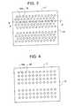
- FIG. 2is a schematic perspective view showing a 2D photonic crystal slab waveguide having two point defects according to another embodiment of the invention.
- FIG. 3is a schematic plan view showing the triangular lattice pattern of the 2D photonic crystal slab waveguide of FIG. 1.
- FIG. 4is a schematic plan view showing the square lattice pattern of the 2D photonic crystal slab waveguide
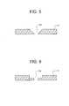
- FIG. 5is a fragmentary cross-sectional view of another form of point defect.
- FIG. 6is a fragmentary cross-sectional view of a further form of point defect.
- FIG. 7is a schematic perspective view of a surface output type wavelength demultiplexer according to the invention.
- FIG. 8is a schematic perspective view of another surface output type wavelength demultiplexer according to the invention.
- FIGS. 9 to 14are cross-sectional views showing successive steps of a process of fabricating a 2D photonic crystal InGaAsP slab waveguide.
- FIGS. 15 to 20are cross-sectional views showing successive steps of another process of fabricating a 2D photonic crystal InGaAsP slab waveguide.
- FIG. 21is a perspective view showing dimensions associated with a 2D photonic crystal.
- FIG. 22is a graph showing the frequency and intensity of light or electromagnetic radiation radiated in the orthogonal direction from the point defect disposed adjacent to the 2D photonic crystal slab waveguide of FIG. 1.
- FIG. 23is a graph showing the frequency and intensity of light or electromagnetic radiation radiated in the orthogonal direction from the two point defects disposed adjacent to the 2D photonic crystal slab waveguide of FIG. 2.
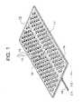
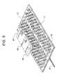
- FIG. 1there is illustrated a waveguide/wavelength demultiplexer according to a first embodiment of the invention in which a point defect is disposed adjacent to a two-dimensional photonic crystal slab waveguide for delivering light or electromagnetic radiation of a selected wavelength in an orthogonal direction.
- a point defectis disposed adjacent to a two-dimensional photonic crystal slab waveguide for delivering light or electromagnetic radiation of a selected wavelength in an orthogonal direction.
- directions parallel and orthogonal to a major surface of the two-dimensional photonic crystal slabare referred to as in-plane and orthogonal directions, respectively.
- the photonic crystal used hereinis a 2D photonic crystal having a bandgap in an in-plane direction due to a 2D periodic distribution of refractive index, and is structured such that cylindrical holes 16 are arrayed in a slab material 11 in a triangular lattice pattern as shown in FIG. 1.
- Incident light or electromagnetic radiation 13( ⁇ 1, ⁇ 2, . . . ⁇ i, . . . ) within the crystal, is prevented by the bandgap from propagating in the in-plane direction, and confined in the orthogonal direction due to total reflection by upper and lower low refractive index materials.
- a line defect 12is incorporated in the photonic crystal by linearly removing some of the cylindrical holes 16 arrayed in the triangular lattice pattern.
- a guided modeexists to form a waveguide.
- the material of which the photonic crystal slab structure is formedis desirably a material having a high refractive index because of the need to confine light or electromagnetic radiation in upward and downward directions.
- an InGaAsP slabis used in the illustrated embodiment, there may be used GaAs, a material containing one or more elements selected from among In, Ga, Al, Sb, As, Ge, Si, P, N, and O, an inorganic material such as Si, especially an inorganic semiconductor material, or an organic material.
- the material used as the slabshould desirably have a higher refractive index as mentioned above, specifically higher than air, preferably at least 2.0, and more preferably at least 3.0.
- the cylindrical holes 16are arrayed in a pattern of triangular lattices 16 a as shown in FIG. 3, although it is possible to use a photonic crystal in which the cylindrical holes 16 are arrayed in a pattern of square lattices 16 b so that a photonic bandgap is present and a defect 12 is linearly incorporated as shown in FIG. 4. It is noted that FIGS. 3 and 4 each are a plan view of a portion of the photonic crystal-constructing slab.
- the light or electromagnetic radiation outlet/inlet portis described.
- light or electromagnetic radiationcan propagate through a defect waveguide in the 2D photonic crystal.
- a linear waveguidethe wavelength range in which light or electromagnetic radiation can be transported at a low loss is relatively wide.
- light or electromagnetic radiation in a wavelength region including the wavelengths of several channelscan be transported through the waveguide.
- a point defect 14is disposed in proximity to the waveguide as shown in FIG. 1, light or electromagnetic radiation of a selected wavelength is trapped within the defect. While resonating within the defect, the light or electromagnetic radiation 15 is radiated in upward and downward directions having a low Q factor due to the slab shape.
- the point defectBy designing the point defect so as to trap only the wavelength of a particular channel in the wavelength region, the point defect functions not only as the light or electromagnetic radiation outlet/inlet port, but also as a demultiplexer, multiplexer or filter for taking out light or electromagnetic radiation of the selected wavelength ( ⁇ i).
- the in-plane guided light or electromagnetic radiationcan be guided in the orthogonal direction, enabling to form a branching or redirecting path within a minute region.
- light or electromagnetic radiation of a selected wavelength incoming in the orthogonal directioncan be guided to the in-plane waveguide.
- FIG. 1In the embodiment of FIG. 1, light or electromagnetic radiation is radiated in upward and downward directions because the defect lacks vertical asymmetry.
- Vertical asymmetrycan be incorporated in the defect so that light or electromagnetic radiation is radiated in either one of upward and downward directions.
- the method of incorporating asymmetryis, for example, by tailoring the shape of the point defect 14 from cylinder to cone as shown in FIG. 5, or by changing the diameter of the point defect 14 between upper and lower levels of the slab 11 as shown in FIG. 6. It is noted that FIGS. 5 and 6 each are a cross-sectional view of a point defect-surrounding portion.
- FIG. 2there is illustrated a second embodiment of the invention wherein two point defects 21 and 22 are disposed adjacent to the linear waveguide. Since the wavelength of light or electromagnetic radiation 22 , 23 to be trapped or radiated is controlled by the size of each defect, two wavelengths ( ⁇ i, ⁇ j) in the region of incident light or electromagnetic radiation ( ⁇ 1, ⁇ 2, . . . , ⁇ i, ⁇ j, . . . ) can be delivered through the respective point defects. The light or electromagnetic radiation other than the trapped and radiated ones is guided through the linear waveguide.
- a two-channel wavelength demultiplexeris illustrated in this embodiment, a multi-channel wavelength demultiplexer can be formed by increasing the number of defects.
- FIG. 7illustrates the concept of a multiplexer/demultiplexer according to a third embodiment of the present invention.
- Light or electromagnetic radiation 31 of a certain wavelength regionpropagates through the photonic crystal waveguide, is trapped by point defects 32 to 34 and delivered in the orthogonal direction.
- the light or electromagnetic radiationis introduced into optical fibers 35 to 37 disposed above the point defects and used as signals.
- the optical fibersare preferably located above the point defects with a sufficient spacing not to cause the photonic crystal structure to be disordered.
- the photonic crystal structuremay be integrated with semiconductor devices having a photoelectric conversion function, for example, photodiode arrays 45 to 47 as shown in FIG. 8.
- semiconductor devices having a photoelectric conversion functionfor example, photodiode arrays 45 to 47 as shown in FIG. 8.
- an InP layer 52 serving as a buffer layer and a layer of a high refractive index material, typically an InGaAsP layer 53are formed by crystal growth. Crystal growth is preferably carried out by the MOCVD method and at 590° to 650° C.
- a photoresist 54 for electron beam patterningis coated as shown in FIG. 10, which is exposed and developed into a resist pattern as shown in FIG. 11.
- Image exposure with electron beamsis employed herein since the lattice constant of the photonic crystal is as small as about 0.5 ⁇ m at most even on the assumption that the light or electromagnetic radiation to be transported has a wavelength in the infrared region.
- cylindrical holes and defectsare formed in the InGaAsP slab by reactive ion etching (RIE) using the resist as a mask.
- RIEreactive ion etching
- the RIEuses a gas mixture of H 2 and CH 4 , for example.
- the resistis then removed as shown in FIG. 13.
- the InGaAsP slabis processed into a membrane as shown in FIG. 14. This is done by wet etching so as to effect selective etching of the InP layer.
- Sisilicon
- the SOI substrateincludes a Si substrate 61 serving as a base and a single crystal Si layer 63 stacked thereon with a SiO 2 layer 62 interposed therebetween.
- a structure having a SiO 2 layer and a Si layer grown on a Si substrateis also employable.
- a photoresist 64 for electron beam patterningis coated as shown in FIG. 16, which is exposed and developed into a resist pattern as shown in FIG. 17.
- cylindrical holes and defectsare formed in the Si layer 63 by reactive ion etching (RIE) using the resist 64 as a mask.
- RIEreactive ion etching
- the RIEuses SF 6 gas.
- the resistis removed as shown in FIG. 19.
- the oxide film layer below the photonic crystalis etched with an aqueous HF solution, leaving a membrane as shown in FIG. 20.
- the photonic crystal slabwas formed of InGaAsP.
- the photonic crystalhas a lattice constant “a,” the holes have a radius r of 0.29a, and the slab has a thickness t of 0.6a.
- ⁇is a permeability
- Eis a dielectric constant
- H x n + 1 2 ⁇ ( i , j + 1 2 , k + 1 2 )H x n - 1 2 ⁇ ( i , j + 1 2 , k + 1 2 ) + ⁇ ⁇ ⁇ t ⁇ ⁇ ( i , j + 1 2 , k + 1 2 ) [ E y n ⁇ ( i , j + 1 2 , k + 1 ) - E y n ⁇ ( i , j + 1 2 , k ) ⁇ ⁇ ⁇ z + E z n ⁇ ( i , j , k + 1 2 ) - E z n ⁇ ( i , j + 1 , k + 1 2 ) - E z n ⁇ ( i , j + 1 , k + 1 2 ) - E z n ⁇ ( i , j + 1 , k + 1 2
- FIG. 23shows the frequency and intensity of light or electromagnetic radiation radiated from each point defect in the embodiment of FIG. 2 wherein point defects of different size are disposed adjacent to the waveguide.
- the Q value of the defectsis approximately 500 in either case.
- a waveguide created by introducing a line defect and a point defect in the 2D photonic crystalhas a function of transmitting light or electromagnetic radiation into and out of the point defect and a function as a wavelength demultiplexer/multiplexer of the plane output type.
- a wavelength demultiplexer fabricated by providing a point defect in proximity to a 2D photonic crystal waveguide according to the inventionis able to input and output light or electromagnetic radiation in the orthogonal direction despite the 2D photonic crystal structure. Since light or electromagnetic radiation of a selected wavelength can be input or output from the point defect in a demultiplexed manner, there can be realized an ultrasmall wavelength demultiplexer. This also enables relatively easy realization of a steric ultrasmall light or electromagnetic circuit.
Landscapes
- Physics & Mathematics (AREA)
- Engineering & Computer Science (AREA)
- Optics & Photonics (AREA)
- Microelectronics & Electronic Packaging (AREA)
- General Physics & Mathematics (AREA)
- Chemical & Material Sciences (AREA)
- Nanotechnology (AREA)
- Life Sciences & Earth Sciences (AREA)
- Biophysics (AREA)
- Crystallography & Structural Chemistry (AREA)
- Optical Integrated Circuits (AREA)
Abstract
Description
- This invention relates to a photonic crystal for use as a ultrasmall optical circuit device, and more particularly, to a two-dimensional photonic crystal having a two-dimensional periodic distribution of refractive index. It further relates to a waveguide having a light or electromagnetic radiation outlet/inlet port created by introducing a line defect and a point defect in such photonic crystal, and a wavelength demultiplexer.[0001]
- With the recent advance of wavelength multiplexing communication systems, wavelength demultiplexers, multiplexers and filters become more important.[0002]
- The optical branching/inserting device for wavelength multiplexing communication systems, also known as optical add/drop multiplexing device, has a function of taking a signal of a certain channel out of multiplexed signals or add the same to an empty channel. General constructions include array waveguide diffraction grating and fiber grating types. The array waveguide diffraction grating is a kind of diffraction grating having an array of a plurality of optical waveguides of different length in which the difference in length between waveguides creates a wavelength-dependent slope of wavefront so that upon input of wavelength-multiplexed light, the light is demultiplexed in terms of wavelength into different waveguides to produce outputs (see Journal of IEICE, pp. 746-749, 1999, for example). In the fiber grating type, only signals of a specific wavelength are taken out of the drop port or introduced from the add port by Bragg reflection at the fiber grating.[0003]
- In the prior art wavelength multiplexers/demultiplexers of the array waveguide diffraction grating type, however, the radius of curvature must be kept significantly large in order to reduce a bend loss, resulting in a very large device size.[0004]
- Many proposals were then made based on the concept of forming an ultrasmall optical multiplexer/demultiplexer using photonic crystal. These proposals are described in, for example, Applied Physics Letters, vol. 75, pp. 3739-3741, 1999 (Reference 1) and Physical Review Letters, vol. 80, pp. 960-963, 1998 (Reference 2).[0005]
- The photonic crystal is a crystal having a periodic distribution of refractive index therein, which enables to establish novel optical characteristics using an artificial periodic structure.[0006]
- One of the important features of the photonic crystal is the presence of a photonic bandgap. In photonic crystal having a three-dimensional periodicity (referred to as a 3D photonic crystal, hereinafter), a full bandgap that prohibits propagation of light in all directions can be formed. This enables local confinement of light, control of spontaneous emission light, and formation of a waveguide by the introduction of a line defect, indicating a possibility to realize an ultrasmall optical circuit.[0007]
- Reference 1 suggests that an ultrasmall light demultiplexer can be formed by branching a waveguide formed by introducing a line defect into a 3D photonic crystal, but does not illustrate any specific structure.[0008]
- Active studies have been made on a photonic crystal having a two-dimensional periodic structure (referred to as a 2D photonic crystal, hereinafter), because its fabrication is relatively easy. Reference 2 describes the analytic results of a demultiplexer using a branched waveguide.[0009]
- A refractive index periodicity structure of 2D photonic crystal is formed by arranging cylindrical holes in a high refractive index material in a square or triangular lattice pattern. Alternatively, it is formed by arranging cylinders of a high refractive index material in a low refractive index material in a square lattice pattern. Photonic bandgaps are formed from these periodicity structures whereby the propagation of in-plane light is controlled. By introducing a line defect into this periodic structure, a waveguide can be created. See, for example, Physical Review Letters, vol. 77, pp. 3787-3790, 1996, and Reference 2.[0010]
- Reference 2 relates to the array of cylinders of a high refractive index material in a square lattice pattern. It is noted that although the propagation of light in the in-plane direction can be controlled by a bandgap as previously described, the propagation of light in upward and downward directions cannot be controlled by the periodic structure. Analysis is thus made on a straight waveguide and a 90° bend branch configuration and branch configuration on the assumption that the height is infinite.[0011]
- However, since it is impossible for an actual device to have an infinite height, light must be confined within a finite height.[0012]
- On the other hand, where cylindrical holes are formed in a high refractive index material, a waveguide can be created by forming the high refractive index material as a slab, and providing low refractive index layers above and below the slab so as to confine light by total reflection.[0013]
- However, no research has been made on multiplexers and demultiplexers of such a structure. Also, no research has been made on the 90° bend branch configuration and branch configuration of guiding light propagating in the in-plane direction to the orthogonal direction or guiding light from the orthogonal direction to the in-plane direction.[0014]
- Optical multiplexers and demultiplexers using a super-prism based on self-organized 3D crystal have also been studied. See, for example, Applied Physics Letters, vol. 74, pp. 1212-1214, 1999 and 0 plus E, December 1999, pp. 1560-1565. They are not combined with waveguides, and only the function of an independent device is investigated.[0015]
- If a photonic crystal waveguide is able to deliver a light output with wavelength selectivity in a certain wavelength region or receive a light input with wavelength selectivity, it becomes possible to realize an optical circuit having a light demultiplexing/multiplexing function of much smaller size than conventional devices. Also, if light or electromagnetic radiation in a 2D photonic crystal waveguide can be guided to the orthogonal direction, a steric light or electromagnetic radiation circuit can be obtained.[0016]
- An object of the invention is to provide a construction capable of guiding or receiving light or electromagnetic radiation propagating through a 2D photonic crystal waveguide in a direction orthogonal to the plane thereof, the construction being effective for forming a light or electromagnetic radiation waveguide or a light or electromagnetic radiation multiplexer/demultiplexer.[0017]
- The above and other objects are attained by the invention which is defined below.[0018]
- (1) A two-dimensional photonic crystal waveguide comprising[0019]
- a two-dimensional photonic crystal structure based on a slab formed of a material having a higher refractive index than air, in which a material having a lower refractive index than the slab material is periodically arrayed to provide a refractive index distribution,[0020]
- a photonic crystal waveguide created by forming a line defect in the periodic array of photonic crystal, the line defect functioning as a waveguide, and[0021]
- at least one point defect disposed adjacent the photonic crystal waveguide to act as a disorder in the periodic array of photonic crystal,[0022]
- wherein the point defect functions as a light or electromagnetic radiation outlet/inlet port for trapping light or electromagnetic radiation of a selected wavelength among light or electromagnetic radiation propagating through the waveguide and radiating it, or trapping light or electromagnetic radiation of a selected wavelength from without the waveguide and introducing it into the waveguide.[0023]
- (2) The two-dimensional photonic crystal waveguide of (1) wherein the light or electromagnetic radiation outlet/inlet port is to radiate or introduce the light or electromagnetic radiation propagating in a direction orthogonal to the slab surface.[0024]
- (3) The two-dimensional photonic crystal waveguide of (1) or (2) wherein the wavelength of light or electromagnetic radiation radiated or introduced by the point defect differs depending on the shape of the point defect.[0025]
- (4) The two-dimensional photonic crystal waveguide of any one of (1) to (3) wherein the array of the lower refractive index material is formed by filling cylindrical holes in the slab with the lower refractive index material.[0026]
- (5) The two-dimensional photonic crystal waveguide of any one of (1) to (4) wherein the array of the lower refractive index material is a triangular lattice array.[0027]
- (6) The two-dimensional photonic crystal waveguide of any one of (1) to (5) wherein the point defect is configured so as to be asymmetric on opposite sides with respect to the slab surface.[0028]
- (7) The two-dimensional photonic crystal waveguide of any one of (1) to (6) wherein the slab material has a refractive index of at least 2.0.[0029]
- (8) The two-dimensional photonic crystal waveguide of (7) wherein the slab material is an inorganic material containing at least one element selected from the group consisting of In, Ga, Al, Sb, As, Ge, Si, P, N, and O or an organic material.[0030]
- (9) The two-dimensional photonic crystal waveguide of any one of (1) to (8) wherein the lower refractive index material is air.[0031]
- (10) A photonic crystal wavelength demultiplexer comprising the two-dimensional photonic crystal waveguide of any one of (1) to (9).[0032]
- (11) The photonic crystal wavelength demultiplexer of (10) wherein there are included a plurality of point defects and wavelength of light or electromagnetic radiation radiated or trapped by each point defect differs.[0033]
- (12) The photonic crystal wavelength demultiplexer of (10) or (11), further comprising an optical fiber disposed in proximity to the point defect.[0034]
- (13) The photonic crystal wavelength demultiplexer of (10) or (11), further comprising a semiconductor device having a photoelectric conversion function disposed in proximity to the point defect.[0035]
- In the 2D photonic crystal waveguide of the invention comprising a 2D photonic crystal structure based on a slab formed of a material having a higher refractive index than air, in which a material having a lower refractive index than the slab material is periodically arrayed to provide a refractive index distribution, a photonic crystal waveguide is created by forming a line defect, which functions as a waveguide, in the periodic array of photonic crystal, and at least one point defect is disposed adjacent the photonic crystal waveguide to act as a disorder in the periodic array of photonic crystal. The point defect functions as a light or electromagnetic radiation outlet/inlet port for trapping light or electromagnetic radiation of a selected wavelength among light or electromagnetic radiation propagating through the waveguide and radiating it, or trapping light or electromagnetic radiation of a selected wavelength from the exterior and introducing it into the waveguide.[0036]
- The waveguide and the point defect according to the invention can transport, receive and deliver not only light, but also electromagnetic radiation having a character approximate to light.[0037]
- Where a point defect is formed in proximity to the waveguide formed by the line defect, introduction and removal of light or electromagnetic radiation into and out of the point defect becomes possible so that a light or electromagnetic radiation inlet/outlet port is available. The point defect becomes a disordered site in the 2D photonic crystal structure based on a slab formed of a material having a higher refractive index than air, in which a material having a lower refractive index than the slab material is periodically arrayed to provide a refractive index distribution.[0038]
- FIG. 1 is a schematic perspective view showing a 2D photonic crystal slab waveguide having one point defect according to one embodiment of the invention.[0039]
- FIG. 2 is a schematic perspective view showing a 2D photonic crystal slab waveguide having two point defects according to another embodiment of the invention.[0040]
- FIG. 3 is a schematic plan view showing the triangular lattice pattern of the 2D photonic crystal slab waveguide of FIG. 1.[0041]
- FIG. 4 is a schematic plan view showing the square lattice pattern of the 2D photonic crystal slab waveguide FIG. 5 is a fragmentary cross-sectional view of another form of point defect.[0042]
- FIG. 6 is a fragmentary cross-sectional view of a further form of point defect.[0043]
- FIG. 7 is a schematic perspective view of a surface output type wavelength demultiplexer according to the invention.[0044]
- FIG. 8 is a schematic perspective view of another surface output type wavelength demultiplexer according to the invention.[0045]
- FIGS.[0046]9 to14 are cross-sectional views showing successive steps of a process of fabricating a 2D photonic crystal InGaAsP slab waveguide.
- FIGS.[0047]15 to20 are cross-sectional views showing successive steps of another process of fabricating a 2D photonic crystal InGaAsP slab waveguide.
- FIG. 21 is a perspective view showing dimensions associated with a 2D photonic crystal.[0048]
- FIG. 22 is a graph showing the frequency and intensity of light or electromagnetic radiation radiated in the orthogonal direction from the point defect disposed adjacent to the 2D photonic crystal slab waveguide of FIG. 1.[0049]
- FIG. 23 is a graph showing the frequency and intensity of light or electromagnetic radiation radiated in the orthogonal direction from the two point defects disposed adjacent to the 2D photonic crystal slab waveguide of FIG. 2.[0050]
- Referring to FIG. 1, there is illustrated a waveguide/wavelength demultiplexer according to a first embodiment of the invention in which a point defect is disposed adjacent to a two-dimensional photonic crystal slab waveguide for delivering light or electromagnetic radiation of a selected wavelength in an orthogonal direction. Throughout the specification, directions parallel and orthogonal to a major surface of the two-dimensional photonic crystal slab are referred to as in-plane and orthogonal directions, respectively.[0051]
- First, the photonic crystal and the waveguide are described. The photonic crystal used herein is a 2D photonic crystal having a bandgap in an in-plane direction due to a 2D periodic distribution of refractive index, and is structured such that[0052]
cylindrical holes 16 are arrayed in aslab material 11 in a triangular lattice pattern as shown in FIG. 1. - Incident light or electromagnetic radiation 13 (λ1, λ2, . . . λi, . . . ) within the crystal, is prevented by the bandgap from propagating in the in-plane direction, and confined in the orthogonal direction due to total reflection by upper and lower low refractive index materials.[0053]
- As shown in FIG. 1, a[0054]
line defect 12 is incorporated in the photonic crystal by linearly removing some of thecylindrical holes 16 arrayed in the triangular lattice pattern. In theline defect 12, a guided mode exists to form a waveguide. - The material of which the photonic crystal slab structure is formed is desirably a material having a high refractive index because of the need to confine light or electromagnetic radiation in upward and downward directions. Although an InGaAsP slab is used in the illustrated embodiment, there may be used GaAs, a material containing one or more elements selected from among In, Ga, Al, Sb, As, Ge, Si, P, N, and O, an inorganic material such as Si, especially an inorganic semiconductor material, or an organic material.[0055]
- The material used as the slab should desirably have a higher refractive index as mentioned above, specifically higher than air, preferably at least 2.0, and more preferably at least 3.0.[0056]
- In the illustrated embodiment, the[0057]
cylindrical holes 16 are arrayed in a pattern oftriangular lattices 16aas shown in FIG. 3, although it is possible to use a photonic crystal in which thecylindrical holes 16 are arrayed in a pattern ofsquare lattices 16bso that a photonic bandgap is present and adefect 12 is linearly incorporated as shown in FIG. 4. It is noted that FIGS. 3 and 4 each are a plan view of a portion of the photonic crystal-constructing slab. - Next, the light or electromagnetic radiation outlet/inlet port is described. As previously described, light or electromagnetic radiation can propagate through a defect waveguide in the 2D photonic crystal. In a linear waveguide, the wavelength range in which light or electromagnetic radiation can be transported at a low loss is relatively wide. Then light or electromagnetic radiation in a wavelength region including the wavelengths of several channels can be transported through the waveguide. By contrast, once a[0058]
point defect 14 is disposed in proximity to the waveguide as shown in FIG. 1, light or electromagnetic radiation of a selected wavelength is trapped within the defect. While resonating within the defect, the light orelectromagnetic radiation 15 is radiated in upward and downward directions having a low Q factor due to the slab shape. - By designing the point defect so as to trap only the wavelength of a particular channel in the wavelength region, the point defect functions not only as the light or electromagnetic radiation outlet/inlet port, but also as a demultiplexer, multiplexer or filter for taking out light or electromagnetic radiation of the selected wavelength (λi). With this configuration, the in-plane guided light or electromagnetic radiation can be guided in the orthogonal direction, enabling to form a branching or redirecting path within a minute region. Inversely, light or electromagnetic radiation of a selected wavelength incoming in the orthogonal direction can be guided to the in-plane waveguide.[0059]
- By appropriately setting the spacing between the waveguide and the point defect, it becomes possible to control the proportion of light or electromagnetic radiation of a selected wavelength to be trapped and radiated. It is then possible to form with ease a light or electromagnetic radiation circuit for taking out or branching a predetermined proportion of light or electromagnetic radiation.[0060]
- In the embodiment of FIG. 1, light or electromagnetic radiation is radiated in upward and downward directions because the defect lacks vertical asymmetry. Vertical asymmetry can be incorporated in the defect so that light or electromagnetic radiation is radiated in either one of upward and downward directions. The method of incorporating asymmetry is, for example, by tailoring the shape of the[0061]
point defect 14 from cylinder to cone as shown in FIG. 5, or by changing the diameter of thepoint defect 14 between upper and lower levels of theslab 11 as shown in FIG. 6. It is noted that FIGS. 5 and 6 each are a cross-sectional view of a point defect-surrounding portion. - Referring to FIG. 2, there is illustrated a second embodiment of the invention wherein two[0062]
point defects electromagnetic radiation - FIG. 7 illustrates the concept of a multiplexer/demultiplexer according to a third embodiment of the present invention. Light or[0063]
electromagnetic radiation 31 of a certain wavelength region propagates through the photonic crystal waveguide, is trapped by point defects32 to34 and delivered in the orthogonal direction. - The light or electromagnetic radiation is introduced into[0064]
optical fibers 35 to37 disposed above the point defects and used as signals. The optical fibers are preferably located above the point defects with a sufficient spacing not to cause the photonic crystal structure to be disordered. - Alternatively, the photonic crystal structure may be integrated with semiconductor devices having a photoelectric conversion function, for example,[0065]
photodiode arrays 45 to47 as shown in FIG. 8. With this construction, light or electromagnetic radiation delivered from the point defects42 to44 in the orthogonal direction can be directly converted into electrical signals within very small areas. - Now it is described how to fabricate a photonic crystal waveguide/wavelength demultiplexer according to one embodiment of the invention.[0066]
- First of all, as shown in FIG. 9, on an[0067]
InP substrate 51, for example, anInP layer 52 serving as a buffer layer and a layer of a high refractive index material, typically anInGaAsP layer 53 are formed by crystal growth. Crystal growth is preferably carried out by the MOCVD method and at 590° to 650° C. - Next, to form a triangular lattice pattern of circular holes and point defects, a[0068]
photoresist 54 for electron beam patterning is coated as shown in FIG. 10, which is exposed and developed into a resist pattern as shown in FIG. 11. Image exposure with electron beams is employed herein since the lattice constant of the photonic crystal is as small as about 0.5 μm at most even on the assumption that the light or electromagnetic radiation to be transported has a wavelength in the infrared region. - Next, as shown in FIG. 12, cylindrical holes and defects are formed in the InGaAsP slab by reactive ion etching (RIE) using the resist as a mask. The RIE uses a gas mixture of H[0069]2and CH4, for example.
- The resist is then removed as shown in FIG. 13. In order to provide air layers having a low refractive index above and below the slab, the InGaAsP slab is processed into a membrane as shown in FIG. 14. This is done by wet etching so as to effect selective etching of the InP layer.[0070]
- Although InGaAsP is used as the high refractive index material in the above example, silicon (Si) is also useful because it has a high refractive index and can be processed by micro-machining. The fabrication method using Si as the slab material is described below.[0071]
- First, there is furnished a silicon-on-insulator (SOI) substrate as shown in FIG. 15. The SOI substrate includes a[0072]
Si substrate 61 serving as a base and a singlecrystal Si layer 63 stacked thereon with a SiO2layer62 interposed therebetween. Instead of the SOI substrate, a structure having a SiO2layer and a Si layer grown on a Si substrate is also employable. Next, aphotoresist 64 for electron beam patterning is coated as shown in FIG. 16, which is exposed and developed into a resist pattern as shown in FIG. 17. - Next, as shown in FIG. 18, cylindrical holes and defects are formed in the[0073]
Si layer 63 by reactive ion etching (RIE) using the resist64 as a mask. The RIE uses SF6gas. Then the resist is removed as shown in FIG. 19. The oxide film layer below the photonic crystal is etched with an aqueous HF solution, leaving a membrane as shown in FIG. 20. - Illustrative examples of the invention are described below together with their characteristics.[0074]
- First described is a photonic crystal. The photonic crystal slab was formed of InGaAsP. For example, as shown in FIG. 21, the photonic crystal has a lattice constant “a,” the holes have a radius r of 0.29a, and the slab has a thickness t of 0.6a.[0075]
- On the slab provided with a line defect and a point defect, analysis was conducted by the finite-difference time-domain (FDTD) method, with the results shown below. It is understood that the FDTD method is a method of directly solving the time-dependent rotational equation among the Maxwell's equations, which is briefly explained below.[0076]
- Herein, μ is a permeability, E is a dielectric constant.[0078]
- Using the above six equations, the way of propagation of light or electromagnetic radiation through the photonic crystal slab can be analyzed. By observing an electric field above the defect and conducting Fourier transformation, its frequency spectrum is obtainable.[0080]
- First described is a linear waveguide with a cylindrical hole corresponding to one period removed. As long as the normalized frequency f is in the range of 0.27 to 0.28 (c/a), light or electromagnetic radiation can propagate through a waveguide without a loss. The lattice constant is determined so that the wavelength of light or electromagnetic radiation to be propagated may meet this condition. In this example, the wavelength of light or electromagnetic radiation to be propagated is set to be 1.55 μm, f=0.275 (c/a) corresponding to the center of the range of 0.27 to 0.28 (c/a) is 1.55 μm, then “a” is computed to be 0.42625 μm from 0.275×1.55 μm.[0081]
- FIG. 22 shows the frequency and intensity of light or electromagnetic radiation radiated in the orthogonal direction from the point defect disposed adjacent to the waveguide. It is understood that the point defect is provided by changing the radius of one cylindrical hole to 0.56a. It is seen from the diagram that light or electromagnetic radiation at the normalized frequency f=0.273 (c/a) is radiated in upward and downward directions. The Q value is approximately 500.[0082]
- FIG. 23 shows the frequency and intensity of light or electromagnetic radiation radiated from each point defect in the embodiment of FIG. 2 wherein point defects of different size are disposed adjacent to the waveguide. In this example, the point defects are cylindrical holes having a radius of 0.56a and 0.58a. It is seen that light or electromagnetic radiation at the frequency f=0.2729 (c/a) and f=0.2769 (c/a) is radiated. The Q value of the defects is approximately 500 in either case.[0083]
- It is confirmed from these results that a waveguide created by introducing a line defect and a point defect in the 2D photonic crystal has a function of transmitting light or electromagnetic radiation into and out of the point defect and a function as a wavelength demultiplexer/multiplexer of the plane output type.[0084]
- A wavelength demultiplexer fabricated by providing a point defect in proximity to a 2D photonic crystal waveguide according to the invention is able to input and output light or electromagnetic radiation in the orthogonal direction despite the 2D photonic crystal structure. Since light or electromagnetic radiation of a selected wavelength can be input or output from the point defect in a demultiplexed manner, there can be realized an ultrasmall wavelength demultiplexer. This also enables relatively easy realization of a steric ultrasmall light or electromagnetic circuit.[0085]
- Japanese Patent Application No. 2000-084869 is incorporated herein by reference.[0086]
- Although some preferred embodiments have been described, many modifications and variations may be made thereto in light of the above teachings. It is therefore to be understood that the invention may be practiced otherwise than as specifically described without departing from the scope of the appended claims.[0087]


Claims (13)
Applications Claiming Priority (2)
| Application Number | Priority Date | Filing Date | Title |
|---|---|---|---|
| JP2000084869AJP3925769B2 (en) | 2000-03-24 | 2000-03-24 | Two-dimensional photonic crystal and multiplexer / demultiplexer |
| JP2000-084869 | 2000-03-24 |
Publications (2)
| Publication Number | Publication Date |
|---|---|
| US20020009277A1true US20020009277A1 (en) | 2002-01-24 |
| US6738551B2 US6738551B2 (en) | 2004-05-18 |
Family
ID=18601287
Family Applications (1)
| Application Number | Title | Priority Date | Filing Date |
|---|---|---|---|
| US09/814,728Expired - LifetimeUS6738551B2 (en) | 2000-03-24 | 2001-03-23 | Two-dimensional photonic crystal, and multiplexer/demultiplexer using the same |
Country Status (5)
| Country | Link |
|---|---|
| US (1) | US6738551B2 (en) |
| EP (1) | EP1136853B1 (en) |
| JP (1) | JP3925769B2 (en) |
| CA (1) | CA2341815C (en) |
| DE (1) | DE60122957T2 (en) |
Cited By (44)
| Publication number | Priority date | Publication date | Assignee | Title |
|---|---|---|---|---|
| US20020191933A1 (en)* | 2001-06-07 | 2002-12-19 | Nec Corporation | Waveguide |
| US6560006B2 (en)* | 2001-04-30 | 2003-05-06 | Agilent Technologies, Inc. | Two-dimensional photonic crystal slab waveguide |
| US20030174993A1 (en)* | 2002-03-13 | 2003-09-18 | Tatsuya Tomaru | Photonic crystal and photonic-crystal waveguide |
| US20040062505A1 (en)* | 2002-09-26 | 2004-04-01 | Mitsubishi Denki Kabushiki Kaisha | Optical active device |
| US20040140478A1 (en)* | 2002-09-09 | 2004-07-22 | Toney James E. | Multi-barrier photonic heterostructure |
| US20040165850A1 (en)* | 2003-02-10 | 2004-08-26 | Kyoto University | Two-dimensional photonic crystal cavity and channel add/drop filter |
| US20040184754A1 (en)* | 2003-03-17 | 2004-09-23 | Kyoto University | Two-Dimensional Photonic Crystal Cavity and Channel Add/Drop Filter |
| US20040184735A1 (en)* | 2003-03-17 | 2004-09-23 | Kyoto University | Channel Add/Drop Filter and Channel Monitor Employing Two-Dimensional Photonic Crystal |
| US20050047742A1 (en)* | 2003-08-28 | 2005-03-03 | Alps Electric Co., Ltd And Kyoto University | Two-dimensional photonic crystal slab, two-dimensional photonic crystal waveguide, and optical device |
| US20050053326A1 (en)* | 2003-09-09 | 2005-03-10 | Toney James E. | Wavelength separation devices incorporating multi-barrier photonic heterostructures |
| US20050078902A1 (en)* | 2003-10-11 | 2005-04-14 | Beausoleil Raymond G. | Photonic interconnect system |
| US20050146778A1 (en)* | 2002-03-26 | 2005-07-07 | Japan Science And Technology Agency | Two-dimensional photonic crystal optical multiplexer/demultiplexer |
| US20050147371A1 (en)* | 2002-03-26 | 2005-07-07 | Japan Science And Technology Agency | Two-dimensional photonic crystal optical resonator and optical reflector using interference between point defects |
| US20050152659A1 (en)* | 2003-11-25 | 2005-07-14 | Ricoh Company, Ltd. | Optical control element |
| US20050220402A1 (en)* | 2004-03-30 | 2005-10-06 | Akinari Takagi | Display element, image observation system having display element, and image projection system |
| US20060034577A1 (en)* | 2004-05-20 | 2006-02-16 | Matsushita Electric Industrial Co., Ltd. | Photonic crystal device |
| US20060051014A1 (en)* | 2002-12-06 | 2006-03-09 | Japan Science And Technology Agency | Two-dimensional photonic crystal optical multiplexer demultiplexer utilizing boundary reflection |
| US20060182400A1 (en)* | 2004-11-15 | 2006-08-17 | Matsushita Electric Industrial Co., Ltd. | Optical waveguide device |
| US20060210233A1 (en)* | 2005-03-15 | 2006-09-21 | Jong-Souk Yeo | Method and apparatus for forming a photonic crystal |
| US20070009219A1 (en)* | 2003-08-29 | 2007-01-11 | Ranko Hatsuda | Two-dimensional photonic crystal having air-bridge structure and method for manufacturing such a crystal |
| US20070172188A1 (en)* | 2004-03-05 | 2007-07-26 | Kyoto University | Two-dimensional photonic crystal |
| US20080002931A1 (en)* | 2004-12-28 | 2008-01-03 | Kyoto University | Two-Dimensional Photonic Crystal and Optical Function Element Using the Same |
| US20080013902A1 (en)* | 2004-08-30 | 2008-01-17 | Kyoto University | Two-Dimensional Photonic Crystal and Optical Device Using the Crystal |
| US20080030657A1 (en)* | 2006-08-04 | 2008-02-07 | Au Optronics Corporation | Color filter and fabricating method thereof |
| US20080050066A1 (en)* | 2006-07-31 | 2008-02-28 | Canon Kabushiki Kaisha | Resonator and device having the same |
| US20080124037A1 (en)* | 2004-12-28 | 2008-05-29 | Kyoto University | Two-Dimensional Photonic Crystal And Optical Device Using The Same |
| CN100430758C (en)* | 2006-09-05 | 2008-11-05 | 友达光电股份有限公司 | Color filter and manufacturing method thereof |
| US7509013B2 (en) | 2005-01-31 | 2009-03-24 | Tdk Corporation | Two-dimensional photonic crystal |
| KR100890868B1 (en)* | 2002-06-27 | 2009-03-27 | 주식회사 케이티 | Photonic waveguide color dispersion compensation device combined with a resonator |
| US20090162008A1 (en)* | 2006-08-28 | 2009-06-25 | Kyoto University | Polarization-independent two-dimensional photonic crystal multiplexer/demultiplexer |
| US20090175572A1 (en)* | 2004-03-25 | 2009-07-09 | Susumu Noda | Photonic crystal having heterostructure and optical device using the photonic crystal |
| EP1607770A4 (en)* | 2003-03-26 | 2009-08-19 | Tdk Corp | Two-dimensional photonic crystal, and waveguide and resonator using the same |
| US20090232441A1 (en)* | 2005-03-18 | 2009-09-17 | Kyoto University | Polarized Light Mode Converter |
| CN102636842A (en)* | 2012-04-19 | 2012-08-15 | 中国振华集团云科电子有限公司 | Photonic crystal filter with three frequency points |
| US20120296060A1 (en)* | 2004-08-19 | 2012-11-22 | Cheng Stephen Z | Photonic crystal, conjugated polymers suitable for photonic crystals, and a method for synthesizing conjugated polymers |
| US20160070059A1 (en)* | 2013-05-01 | 2016-03-10 | Corning Incorporated | Random air line rod |
| CN105891949A (en)* | 2016-05-20 | 2016-08-24 | 上海大学 | Method for preparing two-dimensional photonic crystal based on air column laser etching |
| US20170146737A1 (en)* | 2014-09-29 | 2017-05-25 | Zhengbiao OUYANG | Right-angle waveguide based on circular-hole-type square-lattice photonic crystal and dual compensation scattering cylinders with low refractive index |
| US20170176782A1 (en)* | 2014-09-29 | 2017-06-22 | Shenzhen University | Broadband three-port optical circulator with introduced triangular-guide column |
| USD840404S1 (en) | 2013-03-13 | 2019-02-12 | Nagrastar, Llc | Smart card interface |
| US10382816B2 (en) | 2013-03-13 | 2019-08-13 | Nagrastar, Llc | Systems and methods for performing transport I/O |
| USD864968S1 (en) | 2015-04-30 | 2019-10-29 | Echostar Technologies L.L.C. | Smart card interface |
| US11067746B2 (en) | 2017-08-24 | 2021-07-20 | National University Corporation Yokohama National University | Light deflection device |
| CN113376738A (en)* | 2021-05-25 | 2021-09-10 | 太原理工大学 | Funnel-shaped photonic crystal waveguide structure for realizing optical wave unidirectional transmission |
Families Citing this family (77)
| Publication number | Priority date | Publication date | Assignee | Title |
|---|---|---|---|---|
| US20020027655A1 (en)* | 2000-09-04 | 2002-03-07 | Shigeo Kittaka | Optical device and spectroscopic and polarization separating apparatus using the same |
| EP1512994B1 (en)* | 2000-12-27 | 2007-04-04 | Nippon Telegraph and Telephone Corporation | Photonic crystal waveguide |
| WO2003034118A1 (en)* | 2001-10-17 | 2003-04-24 | Risø National Laboratory | A system for electromagnetic field conversion |
| JP3729134B2 (en)* | 2002-01-29 | 2005-12-21 | 松下電器産業株式会社 | Dual wavelength semiconductor laser light source for optical pickup |
| WO2003075055A1 (en)* | 2002-03-06 | 2003-09-12 | Pirelli & C. S.P.A. | Method for guiding an electromagnetic radiation, in particular in an integrated optical device |
| JP2004006567A (en)* | 2002-03-26 | 2004-01-08 | Japan Science & Technology Corp | Point defect three-dimensional photonic crystal optical resonator |
| US6947649B2 (en)* | 2002-05-31 | 2005-09-20 | Matsushita Electric Industrial Co., Ltd. | Method of adjusting the index of refraction of photonic crystals with laser micromachining to tune transmissions within the bandgap and structure |
| JP2004012780A (en) | 2002-06-06 | 2004-01-15 | Seiko Epson Corp | Optical multiplexer / demultiplexer, optical communication device, and optical communication system |
| US20060153500A1 (en)* | 2002-08-14 | 2006-07-13 | Javier Marti Sendra | Coupling system between dielectric optical guides and planar photonic crystal guides |
| US6999669B2 (en)* | 2002-08-19 | 2006-02-14 | Georgia Tech Research Corporation | Photonic crystals |
| JP2004093787A (en)* | 2002-08-30 | 2004-03-25 | Seiko Epson Corp | Optical switch, optical communication device, and optical communication system |
| JP3568943B2 (en)* | 2002-12-06 | 2004-09-22 | 独立行政法人 科学技術振興機構 | Two-dimensional photonic crystal slab with local three-dimensional structure |
| JP3692354B2 (en)* | 2002-12-26 | 2005-09-07 | 独立行政法人科学技術振興機構 | Electromagnetic frequency filter |
| JP2004233476A (en) | 2003-01-29 | 2004-08-19 | Nec Corp | Photonic crystal optical circuit and its control method |
| JP4236092B2 (en) | 2003-01-31 | 2009-03-11 | Tdk株式会社 | 2D photonic crystal |
| US7263259B2 (en)* | 2003-02-07 | 2007-08-28 | Zetetic Institute | Multiple-source arrays fed by guided-wave structures and resonant guided-wave structure cavities |
| US6873777B2 (en) | 2003-03-10 | 2005-03-29 | Japan Aviation Electronics Industry Limited | Two-dimensional photonic crystal device |
| JP4097568B2 (en) | 2003-06-18 | 2008-06-11 | 日本航空電子工業株式会社 | Optical recording device |
| WO2005008305A1 (en) | 2003-07-18 | 2005-01-27 | Nippon Sheet Glass Company, Limited | Photonic crystal waveguide, homogeneous medium waveguide, and optical device |
| JP4228808B2 (en) | 2003-07-23 | 2009-02-25 | 株式会社日立製作所 | Microspectrometer and microchemical system |
| JP4063740B2 (en)* | 2003-08-29 | 2008-03-19 | 国立大学法人京都大学 | Two-dimensional photonic crystal having air bridge structure and manufacturing method thereof |
| JP3763826B2 (en) | 2003-08-29 | 2006-04-05 | 独立行政法人科学技術振興機構 | 2D photonic crystal multiplexer / demultiplexer |
| EP1666939B1 (en) | 2003-08-29 | 2018-04-04 | Kyoto University | Two-dimensional photonic crystal resonator |
| FR2861854B1 (en)* | 2003-10-30 | 2006-01-13 | Centre Nat Rech Scient | FREQUENCY SELECTIVE LIGHT COUPLING-DECOUPLING DEVICE |
| US7965901B2 (en)* | 2003-10-31 | 2011-06-21 | Hewlett-Packard Development Company, L.P. | Hard imaging methods and devices and optical scanning systems |
| US7964925B2 (en)* | 2006-10-13 | 2011-06-21 | Hewlett-Packard Development Company, L.P. | Photodiode module and apparatus including multiple photodiode modules |
| WO2005057719A1 (en)* | 2003-12-08 | 2005-06-23 | Matsushita Electric Industrial Co., Ltd. | Demultiplexer and multiplexer |
| JP4130799B2 (en) | 2003-12-24 | 2008-08-06 | 三星電子株式会社 | Multi-beam semiconductor laser |
| US7440658B2 (en)* | 2004-03-03 | 2008-10-21 | Japan Science And Technology Agency | Photonic crystal coupling defect waveguide |
| US6990259B2 (en)* | 2004-03-29 | 2006-01-24 | Sru Biosystems, Inc. | Photonic crystal defect cavity biosensor |
| JP4534036B2 (en)* | 2004-09-08 | 2010-09-01 | 国立大学法人京都大学 | Optical head and optical recording / reproducing apparatus |
| WO2006055602A2 (en)* | 2004-11-16 | 2006-05-26 | Canon Kabushiki Kaisha | Light-emitting photonic device |
| US7228042B2 (en)* | 2005-03-04 | 2007-06-05 | International Business Machines Corporation | Method and apparatus for resonant coupling in photonic crystal circuits |
| JP2006251063A (en) | 2005-03-08 | 2006-09-21 | Japan Aviation Electronics Industry Ltd | Optical connector, optical coupling method, and optical element |
| JP2006276388A (en)* | 2005-03-29 | 2006-10-12 | Alps Electric Co Ltd | Photonic crystal slab, photonic crystal waveguide and optical device |
| US7570849B2 (en)* | 2005-06-21 | 2009-08-04 | Hewlett-Packard Development Company, L.P. | Integrated circuit device having optically coupled layers |
| JP2007003969A (en)* | 2005-06-27 | 2007-01-11 | Japan Aviation Electronics Industry Ltd | Optical element |
| US7796849B2 (en)* | 2005-10-25 | 2010-09-14 | Georgia Tech Research Corporation | Spatial separation of optical frequency components using photonic crystals |
| JP4684861B2 (en)* | 2005-11-14 | 2011-05-18 | キヤノン株式会社 | Waveguide and device having the same |
| JP4689441B2 (en)* | 2005-11-14 | 2011-05-25 | キヤノン株式会社 | Waveguide and device having the same |
| JP4621920B2 (en)* | 2006-01-18 | 2011-02-02 | 国立大学法人京都大学 | Two-dimensional photonic crystal manufacturing method |
| JP4900572B2 (en) | 2006-03-20 | 2012-03-21 | 国立大学法人京都大学 | 2D photonic crystal |
| JP2008233769A (en)* | 2007-03-23 | 2008-10-02 | Tohoku Univ | Optical filter device and manufacturing method thereof |
| JP5272173B2 (en) | 2007-03-26 | 2013-08-28 | 国立大学法人京都大学 | 2D photonic crystal |
| US20100279886A1 (en)* | 2007-04-03 | 2010-11-04 | University Of Rochester | Two-dimensional photonic bandgap structures for ultrahigh-sensitivity biosensing |
| US8059924B1 (en)* | 2007-09-13 | 2011-11-15 | Lawrence Livermore National Security, Llc | Multiplexed photonic membranes and related detection methods for chemical and/or biological sensing applications |
| WO2009107427A1 (en)* | 2008-02-28 | 2009-09-03 | 日本電気株式会社 | Optical waveguide |
| US7991289B2 (en)* | 2008-03-28 | 2011-08-02 | Raytheon Company | High bandwidth communication system and method |
| US8986558B2 (en) | 2008-09-01 | 2015-03-24 | Japan Science And Technology Agency | Plasma etching method, plasma etching device, and method for producing photonic crystal |
| US8830450B2 (en) | 2009-12-02 | 2014-09-09 | Lawrence Livermore National Security, Llc | Methods and systems for Raman and optical cross-interrogation in flow-through silicon membranes |
| US8947657B2 (en) | 2008-09-08 | 2015-02-03 | Lawrence Livermore National Security, Llc | Methods for isolation and viability assessment of biological organisms |
| WO2010102643A1 (en)* | 2009-03-11 | 2010-09-16 | MAX-PLANCK-Gesellschaft zur Förderung der Wissenschaften e.V. | Tunable optical guided-mode filter device |
| CA2805851C (en) | 2009-10-08 | 2017-03-07 | Adam K. Fontecchio | Led lighting system |
| EP2488912B1 (en) | 2009-10-12 | 2019-07-24 | The Trustees Of Columbia University In The City Of New York | Waveguide comprising photonic crystal for outcoupling light of specific wavelengths |
| US8786852B2 (en)* | 2009-12-02 | 2014-07-22 | Lawrence Livermore National Security, Llc | Nanoscale array structures suitable for surface enhanced raman scattering and methods related thereto |
| CN102540329B (en)* | 2012-01-31 | 2013-01-23 | 中国科学院长春光学精密机械与物理研究所 | Two-dimensional side coupling photonic crystal waveguide single-channel system |
| JP2013160623A (en)* | 2012-02-03 | 2013-08-19 | Tokyo Institute Of Technology | Light measuring apparatus |
| US9395304B2 (en) | 2012-03-01 | 2016-07-19 | Lawrence Livermore National Security, Llc | Nanoscale structures on optical fiber for surface enhanced Raman scattering and methods related thereto |
| EP2891019B1 (en) | 2012-08-28 | 2020-03-04 | Delos Living, LLC | Systems and methods for enhancing wellness associated with habitable environments |
| CN103176328B (en)* | 2013-04-11 | 2015-04-08 | 青岛大学 | Two-dimensional silicon substrate photonic crystal line-defect slow optical waveguide device |
| EP3754588B1 (en) | 2014-02-28 | 2023-08-16 | Delos Living LLC | Systems, methods, and articles for enhancing wellness associated with habitable environments |
| EP3245631A4 (en) | 2015-01-13 | 2018-06-27 | Delos Living, LLC | Systems, methods and articles for monitoring and enhancing human wellness |
| WO2017058770A2 (en) | 2015-09-29 | 2017-04-06 | Chromation Inc. | Nanostructure based article, optical sensor and analytical instrument and method of forming same |
| EP3455597B1 (en) | 2016-05-10 | 2024-11-27 | Chromation Inc. | Integration of optical components within a folded optical path |
| CN105911646B (en)* | 2016-06-13 | 2018-08-21 | 南京邮电大学 | A kind of wavelength-division mould based on photonic crystal divides hybrid multiplex demultiplexer and method |
| EP3504942A4 (en) | 2016-08-24 | 2020-07-15 | Delos Living LLC | SYSTEMS, METHODS AND ARTICLES FOR IMPROVING WELL-BEING IN LIVABLE ENVIRONMENTS |
| WO2019046580A1 (en) | 2017-08-30 | 2019-03-07 | Delos Living Llc | Systems, methods and articles for assessing and/or improving health and well-being |
| US11649977B2 (en) | 2018-09-14 | 2023-05-16 | Delos Living Llc | Systems and methods for air remediation |
| CN109669240B (en)* | 2019-01-04 | 2020-10-02 | 深圳大学 | Photonic crystal waveguide hexapole splitting mode interference FANO resonance structure |
| US11844163B2 (en) | 2019-02-26 | 2023-12-12 | Delos Living Llc | Method and apparatus for lighting in an office environment |
| US11169426B2 (en) | 2019-03-19 | 2021-11-09 | Analog Devices, Inc. | Liquid crystal waveguide with sub-aperture light coupling |
| WO2020198183A1 (en) | 2019-03-25 | 2020-10-01 | Delos Living Llc | Systems and methods for acoustic monitoring |
| JP7274608B2 (en)* | 2020-07-20 | 2023-05-16 | 日本碍子株式会社 | Optical scanning element |
| WO2022076438A1 (en) | 2020-10-06 | 2022-04-14 | Chromation Inc. | Systems and methods to redistribute field of view in spectroscopy |
| JP7599638B2 (en)* | 2021-02-01 | 2024-12-16 | 国立大学法人東京科学大学 | Topological vertical coupler |
| DE102022106271A1 (en)* | 2022-03-17 | 2023-09-21 | Ams-Osram International Gmbh | OPTOELECTRONIC MODULE AND METHOD FOR OPERATING AN OPTOELECTRONIC MODULE |
| WO2024176971A1 (en)* | 2023-02-24 | 2024-08-29 | 公立大学法人大阪 | Method for producing photonic device, and photonic device |
Citations (2)
| Publication number | Priority date | Publication date | Assignee | Title |
|---|---|---|---|---|
| US5526449A (en)* | 1993-01-08 | 1996-06-11 | Massachusetts Institute Of Technology | Optoelectronic integrated circuits and method of fabricating and reducing losses using same |
| US5784400A (en)* | 1995-02-28 | 1998-07-21 | Massachusetts Institute Of Technology | Resonant cavities employing two dimensionally periodic dielectric materials |
Family Cites Families (4)
| Publication number | Priority date | Publication date | Assignee | Title |
|---|---|---|---|---|
| US6101300A (en)* | 1997-06-09 | 2000-08-08 | Massachusetts Institute Of Technology | High efficiency channel drop filter with absorption induced on/off switching and modulation |
| JPH11218627A (en)* | 1998-02-02 | 1999-08-10 | Nippon Telegr & Teleph Corp <Ntt> | Photonic crystal waveguide and method of manufacturing the same |
| JPH11330619A (en)* | 1998-05-18 | 1999-11-30 | Nippon Telegr & Teleph Corp <Ntt> | Optical device |
| US6468823B1 (en)* | 1999-09-30 | 2002-10-22 | California Institute Of Technology | Fabrication of optical devices based on two dimensional photonic crystal structures and apparatus made thereby |
- 2000
- 2000-03-24JPJP2000084869Apatent/JP3925769B2/ennot_activeExpired - Lifetime
- 2001
- 2001-03-19EPEP01106812Apatent/EP1136853B1/ennot_activeExpired - Lifetime
- 2001-03-19DEDE60122957Tpatent/DE60122957T2/ennot_activeExpired - Lifetime
- 2001-03-23USUS09/814,728patent/US6738551B2/ennot_activeExpired - Lifetime
- 2001-03-23CACA002341815Apatent/CA2341815C/ennot_activeExpired - Fee Related
Patent Citations (2)
| Publication number | Priority date | Publication date | Assignee | Title |
|---|---|---|---|---|
| US5526449A (en)* | 1993-01-08 | 1996-06-11 | Massachusetts Institute Of Technology | Optoelectronic integrated circuits and method of fabricating and reducing losses using same |
| US5784400A (en)* | 1995-02-28 | 1998-07-21 | Massachusetts Institute Of Technology | Resonant cavities employing two dimensionally periodic dielectric materials |
Cited By (86)
| Publication number | Priority date | Publication date | Assignee | Title |
|---|---|---|---|---|
| US6560006B2 (en)* | 2001-04-30 | 2003-05-06 | Agilent Technologies, Inc. | Two-dimensional photonic crystal slab waveguide |
| US20020191933A1 (en)* | 2001-06-07 | 2002-12-19 | Nec Corporation | Waveguide |
| US6795621B2 (en)* | 2001-06-07 | 2004-09-21 | Nec Corporation | Waveguide comprising a connection of a photonic-crystal line-defect-waveguide to a total reflection confinement waveguide |
| US6879766B2 (en)* | 2002-03-13 | 2005-04-12 | Hitachi, Ltd. | Photonic crystal and photonic-crystal waveguide |
| US20030174993A1 (en)* | 2002-03-13 | 2003-09-18 | Tatsuya Tomaru | Photonic crystal and photonic-crystal waveguide |
| US20050146778A1 (en)* | 2002-03-26 | 2005-07-07 | Japan Science And Technology Agency | Two-dimensional photonic crystal optical multiplexer/demultiplexer |
| CN1295526C (en)* | 2002-03-26 | 2007-01-17 | 独立行政法人科学技术振兴机构 | Two-dimensional photonic crystal optical resonator and optical reflector using interference between point defects |
| CN1297829C (en)* | 2002-03-26 | 2007-01-31 | 独立行政法人科学技术振兴机构 | Two-dimensional photonic crystal optical multiplexer/demultiplexer |
| US20050147371A1 (en)* | 2002-03-26 | 2005-07-07 | Japan Science And Technology Agency | Two-dimensional photonic crystal optical resonator and optical reflector using interference between point defects |
| US6996319B2 (en) | 2002-03-26 | 2006-02-07 | Japan Science And Technology Agency | Two-dimensional photonic crystal optical resonator and optical reflector using interference between point defects |
| US7590325B2 (en) | 2002-03-26 | 2009-09-15 | Japan Science And Technology Agency | Two-dimensional photonic crystal optical multiplexer/demultiplexer |
| KR100890868B1 (en)* | 2002-06-27 | 2009-03-27 | 주식회사 케이티 | Photonic waveguide color dispersion compensation device combined with a resonator |
| US20040140478A1 (en)* | 2002-09-09 | 2004-07-22 | Toney James E. | Multi-barrier photonic heterostructure |
| US6940637B2 (en) | 2002-09-09 | 2005-09-06 | Battelle Memorial Institute | Multi-barrier photonic heterostructures |
| US7181120B2 (en) | 2002-09-26 | 2007-02-20 | Mitsubishi Denki Kabushiki Kaisha | Optical active device |
| US20040062505A1 (en)* | 2002-09-26 | 2004-04-01 | Mitsubishi Denki Kabushiki Kaisha | Optical active device |
| US7224862B2 (en)* | 2002-12-06 | 2007-05-29 | Japan Science And Technology Agency | Two-dimensional photonic crystal optical multiplexer/demultiplexer using boundary reflection |
| US20060051014A1 (en)* | 2002-12-06 | 2006-03-09 | Japan Science And Technology Agency | Two-dimensional photonic crystal optical multiplexer demultiplexer utilizing boundary reflection |
| US7120344B2 (en) | 2003-02-10 | 2006-10-10 | Sumitomo Electric Industries, Ltd. | Two-dimensional photonic crystal cavity and channel add/drop filter |
| US20040165850A1 (en)* | 2003-02-10 | 2004-08-26 | Kyoto University | Two-dimensional photonic crystal cavity and channel add/drop filter |
| CN100346183C (en)* | 2003-03-17 | 2007-10-31 | 京都大学长 | Channel current filter and monitor by two-dimensional photo crystal |
| US20040184735A1 (en)* | 2003-03-17 | 2004-09-23 | Kyoto University | Channel Add/Drop Filter and Channel Monitor Employing Two-Dimensional Photonic Crystal |
| US20040184754A1 (en)* | 2003-03-17 | 2004-09-23 | Kyoto University | Two-Dimensional Photonic Crystal Cavity and Channel Add/Drop Filter |
| US7046878B2 (en) | 2003-03-17 | 2006-05-16 | President, Kyoto University | Channel add/drop filter and channel monitor employing two-dimensional photonic crystal |
| EP1607770A4 (en)* | 2003-03-26 | 2009-08-19 | Tdk Corp | Two-dimensional photonic crystal, and waveguide and resonator using the same |
| US7336879B2 (en)* | 2003-08-28 | 2008-02-26 | Alps Electric Co., Ltd. | Two-dimensional photonic crystal slab, two-dimensional photonic crystal waveguide, and optical device |
| US20050047742A1 (en)* | 2003-08-28 | 2005-03-03 | Alps Electric Co., Ltd And Kyoto University | Two-dimensional photonic crystal slab, two-dimensional photonic crystal waveguide, and optical device |
| US7333703B2 (en) | 2003-08-29 | 2008-02-19 | Kyoto University | Two-dimensional photonic crystal having air-bridge structure and method for manufacturing such a crystal |
| US20070009219A1 (en)* | 2003-08-29 | 2007-01-11 | Ranko Hatsuda | Two-dimensional photonic crystal having air-bridge structure and method for manufacturing such a crystal |
| US20080145012A1 (en)* | 2003-08-29 | 2008-06-19 | Kyoto University | Two-dimensional photonic crystal having air-bridge structure and method for manufacturing such a crystal |
| US7509014B2 (en) | 2003-08-29 | 2009-03-24 | Kyoto University | Two-dimensional photonic crystal having air-bridge structure and method for manufacturing such a crystal |
| US20050053326A1 (en)* | 2003-09-09 | 2005-03-10 | Toney James E. | Wavelength separation devices incorporating multi-barrier photonic heterostructures |
| US6934441B2 (en) | 2003-09-09 | 2005-08-23 | Battelle Memorial Institute | Wavelength separation devices incorporating multi-barrier photonic heterostructures |
| US20080112665A1 (en)* | 2003-10-11 | 2008-05-15 | Beausoleil Raymond G | Photonic interconnect system |
| US7657137B2 (en)* | 2003-10-11 | 2010-02-02 | Hewlett-Packard Development Company, L.P. | Photonic interconnect system |
| US20050078902A1 (en)* | 2003-10-11 | 2005-04-14 | Beausoleil Raymond G. | Photonic interconnect system |
| US20080112703A1 (en)* | 2003-10-11 | 2008-05-15 | Beausoleil Raymond G | Photonic interconnect system |
| US7546004B2 (en)* | 2003-10-11 | 2009-06-09 | Hewlett-Packard Development Company, L.P. | Photonic interconnect system |
| US7343059B2 (en)* | 2003-10-11 | 2008-03-11 | Hewlett-Packard Development Company, L.P. | Photonic interconnect system |
| US8447146B2 (en)* | 2003-10-11 | 2013-05-21 | Hewlett-Packard Development Company, L.P. | Photonic interconnect method |
| US20080131047A1 (en)* | 2003-10-11 | 2008-06-05 | Beausoleil Raymond G | Photonic interconnect system |
| US20080118201A1 (en)* | 2003-10-11 | 2008-05-22 | Beausoleil Raymond G | Photonic interconnect method |
| US20050152659A1 (en)* | 2003-11-25 | 2005-07-14 | Ricoh Company, Ltd. | Optical control element |
| US7123804B2 (en)* | 2003-11-25 | 2006-10-17 | Ricoh Company, Ltd | Optical control element |
| US7853111B2 (en) | 2004-03-05 | 2010-12-14 | Kyoto University | Two-dimensional photonic crystal |
| US20070172188A1 (en)* | 2004-03-05 | 2007-07-26 | Kyoto University | Two-dimensional photonic crystal |
| US7738749B2 (en) | 2004-03-25 | 2010-06-15 | Kyoto University | Photonic crystal having heterostructure and optical device using the photonic crystal |
| US20090175572A1 (en)* | 2004-03-25 | 2009-07-09 | Susumu Noda | Photonic crystal having heterostructure and optical device using the photonic crystal |
| EP1585087A1 (en)* | 2004-03-30 | 2005-10-12 | Canon Kabushiki Kaisha | Display element, image observation system having display element, and image projection system |
| US20050220402A1 (en)* | 2004-03-30 | 2005-10-06 | Akinari Takagi | Display element, image observation system having display element, and image projection system |
| US7039287B2 (en)* | 2004-03-30 | 2006-05-02 | Canon Kabushiki Kaisha | Display element, image observation system having display element, and image projection system |
| US7120322B2 (en)* | 2004-05-20 | 2006-10-10 | Matsushita Electric Industrial Co., Ltd. | Photonic crystal device |
| US20060034577A1 (en)* | 2004-05-20 | 2006-02-16 | Matsushita Electric Industrial Co., Ltd. | Photonic crystal device |
| US9206285B2 (en)* | 2004-08-19 | 2015-12-08 | The University Of Akron | Photonic crystal, conjugated polymers suitable for photonic crystals, and a method for synthesizing conjugated polymers |
| US20120296060A1 (en)* | 2004-08-19 | 2012-11-22 | Cheng Stephen Z | Photonic crystal, conjugated polymers suitable for photonic crystals, and a method for synthesizing conjugated polymers |
| US20080013902A1 (en)* | 2004-08-30 | 2008-01-17 | Kyoto University | Two-Dimensional Photonic Crystal and Optical Device Using the Crystal |
| US7711228B2 (en) | 2004-08-30 | 2010-05-04 | Kyoto University | Two-dimensional photonic crystal and optical device using the crystal |
| CN100427980C (en)* | 2004-11-15 | 2008-10-22 | 松下电器产业株式会社 | Optical waveguide components |
| US7200312B2 (en) | 2004-11-15 | 2007-04-03 | Matsushita Electric Industrial Co., Ltd. | Optical waveguide device |
| US20060182400A1 (en)* | 2004-11-15 | 2006-08-17 | Matsushita Electric Industrial Co., Ltd. | Optical waveguide device |
| US20080002931A1 (en)* | 2004-12-28 | 2008-01-03 | Kyoto University | Two-Dimensional Photonic Crystal and Optical Function Element Using the Same |
| US20080124037A1 (en)* | 2004-12-28 | 2008-05-29 | Kyoto University | Two-Dimensional Photonic Crystal And Optical Device Using The Same |
| US7912335B2 (en) | 2004-12-28 | 2011-03-22 | Kyoto University | Two-dimensional photonic crystal and optical device using the same |
| US7428352B2 (en) | 2004-12-28 | 2008-09-23 | Kyoto University | Two-dimensional photonic crystal and optical function element using the same |
| US7509013B2 (en) | 2005-01-31 | 2009-03-24 | Tdk Corporation | Two-dimensional photonic crystal |
| US20060210233A1 (en)* | 2005-03-15 | 2006-09-21 | Jong-Souk Yeo | Method and apparatus for forming a photonic crystal |
| US7389023B2 (en)* | 2005-03-15 | 2008-06-17 | Hewlett-Packard Development Company, L.P. | Method and apparatus for forming a photonic crystal |
| US7783139B2 (en) | 2005-03-18 | 2010-08-24 | Kyoto University | Polarized light mode converter |
| US20090232441A1 (en)* | 2005-03-18 | 2009-09-17 | Kyoto University | Polarized Light Mode Converter |
| US7587118B2 (en)* | 2006-07-31 | 2009-09-08 | Canon Kabushiki Kaisha | Resonator and device having the same |
| US20080050066A1 (en)* | 2006-07-31 | 2008-02-28 | Canon Kabushiki Kaisha | Resonator and device having the same |
| US20080030657A1 (en)* | 2006-08-04 | 2008-02-07 | Au Optronics Corporation | Color filter and fabricating method thereof |
| US7595512B2 (en) | 2006-08-04 | 2009-09-29 | Au Optronics Corporation | Color filter and fabricating method thereof |
| US20090162008A1 (en)* | 2006-08-28 | 2009-06-25 | Kyoto University | Polarization-independent two-dimensional photonic crystal multiplexer/demultiplexer |
| US7715668B2 (en) | 2006-08-28 | 2010-05-11 | Kyoto University | Polarization-independent two-dimensional photonic crystal multiplexer/demultiplexer |
| CN100430758C (en)* | 2006-09-05 | 2008-11-05 | 友达光电股份有限公司 | Color filter and manufacturing method thereof |
| CN102636842A (en)* | 2012-04-19 | 2012-08-15 | 中国振华集团云科电子有限公司 | Photonic crystal filter with three frequency points |
| USD840404S1 (en) | 2013-03-13 | 2019-02-12 | Nagrastar, Llc | Smart card interface |
| US10382816B2 (en) | 2013-03-13 | 2019-08-13 | Nagrastar, Llc | Systems and methods for performing transport I/O |
| US20160070059A1 (en)* | 2013-05-01 | 2016-03-10 | Corning Incorporated | Random air line rod |
| US20170146737A1 (en)* | 2014-09-29 | 2017-05-25 | Zhengbiao OUYANG | Right-angle waveguide based on circular-hole-type square-lattice photonic crystal and dual compensation scattering cylinders with low refractive index |
| US20170176782A1 (en)* | 2014-09-29 | 2017-06-22 | Shenzhen University | Broadband three-port optical circulator with introduced triangular-guide column |
| USD864968S1 (en) | 2015-04-30 | 2019-10-29 | Echostar Technologies L.L.C. | Smart card interface |
| CN105891949A (en)* | 2016-05-20 | 2016-08-24 | 上海大学 | Method for preparing two-dimensional photonic crystal based on air column laser etching |
| US11067746B2 (en) | 2017-08-24 | 2021-07-20 | National University Corporation Yokohama National University | Light deflection device |
| CN113376738A (en)* | 2021-05-25 | 2021-09-10 | 太原理工大学 | Funnel-shaped photonic crystal waveguide structure for realizing optical wave unidirectional transmission |
Also Published As
| Publication number | Publication date |
|---|---|
| JP3925769B2 (en) | 2007-06-06 |
| EP1136853B1 (en) | 2006-09-13 |
| DE60122957D1 (en) | 2006-10-26 |
| DE60122957T2 (en) | 2007-09-06 |
| EP1136853A1 (en) | 2001-09-26 |
| CA2341815C (en) | 2005-06-28 |
| US6738551B2 (en) | 2004-05-18 |
| JP2001272555A (en) | 2001-10-05 |
| CA2341815A1 (en) | 2001-09-24 |
Similar Documents
| Publication | Publication Date | Title |
|---|---|---|
| US6738551B2 (en) | Two-dimensional photonic crystal, and multiplexer/demultiplexer using the same | |
| JP3847261B2 (en) | Resonator and wavelength multiplexer / demultiplexer in two-dimensional photonic crystal | |
| CA2248042C (en) | Optical diffraction grating | |
| EP2513693B1 (en) | Photonic integrated circuit having a waveguide-grating coupler | |
| US6580863B2 (en) | System and method for providing integrated optical waveguide device | |
| KR100578683B1 (en) | Optical device and its manufacturing method | |
| KR101333418B1 (en) | A polarization diversity grating coupler comprising a two dimensional grating | |
| US6832033B2 (en) | Hetero-structure photonic bandgap materials | |
| US7269310B2 (en) | Optical connector, optical coupling method and optical element | |
| US20080063339A1 (en) | Scalable and defect-tolerant color-center-based quantum computer architectures and methods for fabricating color-center-based quantum computer architectures | |
| JP3459827B2 (en) | Two-dimensional photonic crystal optical multiplexer / demultiplexer | |
| JP4669923B2 (en) | Polarization mode converter | |
| US20020191905A1 (en) | Multi-channel wavelength division multiplexing using photonic crystals | |
| EP1521987B1 (en) | Photonic crystal waveguide | |
| JP4171326B2 (en) | Resonator and wavelength multiplexer / demultiplexer in two-dimensional photonic crystal | |
| US6782169B2 (en) | System for efficient coupling to photonic crystal waveguides | |
| US7110641B2 (en) | Device for directional and wavelength-selective optical coupling | |
| JP2004012780A (en) | Optical multiplexer / demultiplexer, optical communication device, and optical communication system | |
| KR20060123753A (en) | Frequency Selective Optocoupler-Separator Device | |
| US6650796B2 (en) | Waveguide optical frequency router | |
| US6522811B1 (en) | Arrayed waveguide grating | |
| JP2001059917A (en) | Waveguide type optical multiplexer/demultiplexer | |
| JPH08201638A (en) | Optical multiplexer / demultiplexer | |
| JPH1010589A (en) | Optical demultiplexing / multiplexing device |
Legal Events
| Date | Code | Title | Description |
|---|---|---|---|
| AS | Assignment | Owner name:TDK CORPORATION, JAPAN Free format text:ASSIGNMENT OF ASSIGNORS INTEREST;ASSIGNORS:NODA, SUSUMU;CHUTINAN, ALONGKARN;MIYAUCHI, DAISUKE;AND OTHERS;REEL/FRAME:012016/0621;SIGNING DATES FROM 20010620 TO 20010702 Owner name:KANSAI TECHNOLOGY LICENSING ORGANIZATION CO., LTD. Free format text:ASSIGNMENT OF ASSIGNORS INTEREST;ASSIGNORS:NODA, SUSUMU;CHUTINAN, ALONGKARN;MIYAUCHI, DAISUKE;AND OTHERS;REEL/FRAME:012016/0621;SIGNING DATES FROM 20010620 TO 20010702 | |
| FEPP | Fee payment procedure | Free format text:PAYER NUMBER DE-ASSIGNED (ORIGINAL EVENT CODE: RMPN); ENTITY STATUS OF PATENT OWNER: LARGE ENTITY Free format text:PAYOR NUMBER ASSIGNED (ORIGINAL EVENT CODE: ASPN); ENTITY STATUS OF PATENT OWNER: LARGE ENTITY | |
| STCF | Information on status: patent grant | Free format text:PATENTED CASE | |
| CC | Certificate of correction | ||
| FPAY | Fee payment | Year of fee payment:4 | |
| AS | Assignment | Owner name:KYOTO UNIVERSITY, JAPAN Free format text:ASSIGNMENT OF ASSIGNORS INTEREST;ASSIGNOR:KANSAI TECHNOLOGY LICENSING ORGANIZATION CO., LTD.;REEL/FRAME:020525/0225 Effective date:20080204 | |
| FPAY | Fee payment | Year of fee payment:8 | |
| AS | Assignment | Owner name:JAPAN SCIENCE AND TECHNOLOGY AGENCY, JAPAN Free format text:ASSIGNMENT OF ASSIGNORS INTEREST;ASSIGNOR:KYOTO UNIVERSITY;REEL/FRAME:036898/0802 Effective date:20151017 | |
| FPAY | Fee payment | Year of fee payment:12 |