US20020008270A1 - Diffusion barrier layers and methods of forming same - Google Patents
Diffusion barrier layers and methods of forming sameDownload PDFInfo
- Publication number
- US20020008270A1 US20020008270A1US09/942,200US94220001AUS2002008270A1US 20020008270 A1US20020008270 A1US 20020008270A1US 94220001 AUS94220001 AUS 94220001AUS 2002008270 A1US2002008270 A1US 2002008270A1
- Authority
- US
- United States
- Prior art keywords
- platinum
- ruthenium
- electrode
- alloy
- range
- Prior art date
- Legal status (The legal status is an assumption and is not a legal conclusion. Google has not performed a legal analysis and makes no representation as to the accuracy of the status listed.)
- Abandoned
Links
- 238000000034methodMethods0.000titleclaimsabstractdescription71
- 230000004888barrier functionEffects0.000titleclaimsabstractdescription70
- 238000009792diffusion processMethods0.000titledescription22
- BASFCYQUMIYNBI-UHFFFAOYSA-NplatinumChemical compound[Pt]BASFCYQUMIYNBI-UHFFFAOYSA-N0.000claimsabstractdescription266
- 229910052697platinumInorganic materials0.000claimsabstractdescription121
- KJTLSVCANCCWHF-UHFFFAOYSA-NRutheniumChemical compound[Ru]KJTLSVCANCCWHF-UHFFFAOYSA-N0.000claimsabstractdescription79
- 229910052707rutheniumInorganic materials0.000claimsabstractdescription62
- 239000003990capacitorSubstances0.000claimsabstractdescription51
- 239000000758substrateSubstances0.000claimsabstractdescription38
- 239000000956alloySubstances0.000claimsabstractdescription36
- 229910052710siliconInorganic materials0.000claimsabstractdescription30
- XUIMIQQOPSSXEZ-UHFFFAOYSA-NSiliconChemical compound[Si]XUIMIQQOPSSXEZ-UHFFFAOYSA-N0.000claimsabstractdescription29
- 239000010703siliconSubstances0.000claimsabstractdescription29
- 229910045601alloyInorganic materials0.000claimsabstractdescription27
- 238000005229chemical vapour depositionMethods0.000claimsabstractdescription25
- 210000000352storage cellAnatomy0.000claimsabstractdescription20
- 230000015572biosynthetic processEffects0.000claimsabstractdescription18
- 238000004519manufacturing processMethods0.000claimsabstractdescription7
- 239000010410layerSubstances0.000claimsdescription164
- 229910000929Ru alloyInorganic materials0.000claimsdescription54
- 239000000463materialSubstances0.000claimsdescription22
- 239000003989dielectric materialSubstances0.000claimsdescription16
- 229910052751metalInorganic materials0.000claimsdescription16
- 239000002184metalSubstances0.000claimsdescription16
- 238000000151depositionMethods0.000claimsdescription14
- 239000004065semiconductorSubstances0.000claimsdescription13
- 150000002739metalsChemical class0.000claimsdescription7
- 230000015654memoryEffects0.000claimsdescription6
- 229910001092metal group alloyInorganic materials0.000claimsdescription6
- 229910021332silicideInorganic materials0.000claimsdescription6
- 210000004027cellAnatomy0.000claimsdescription5
- 150000004767nitridesChemical class0.000claimsdescription4
- 239000002356single layerSubstances0.000claimsdescription2
- 239000007789gasSubstances0.000description23
- 239000002243precursorSubstances0.000description23
- 238000006243chemical reactionMethods0.000description19
- 230000008569processEffects0.000description17
- QVGXLLKOCUKJST-UHFFFAOYSA-Natomic oxygenChemical compound[O]QVGXLLKOCUKJST-UHFFFAOYSA-N0.000description16
- 229910052760oxygenInorganic materials0.000description16
- 239000001301oxygenSubstances0.000description16
- 239000000376reactantSubstances0.000description11
- -1i.e.Substances0.000description10
- 239000004020conductorSubstances0.000description9
- 230000008021depositionEffects0.000description8
- 239000000203mixtureSubstances0.000description7
- XKRFYHLGVUSROY-UHFFFAOYSA-NArgonChemical compound[Ar]XKRFYHLGVUSROY-UHFFFAOYSA-N0.000description6
- 229910001925ruthenium oxideInorganic materials0.000description5
- WOCIAKWEIIZHES-UHFFFAOYSA-Nruthenium(iv) oxideChemical compoundO=[Ru]=OWOCIAKWEIIZHES-UHFFFAOYSA-N0.000description5
- 235000012431wafersNutrition0.000description5
- VYPSYNLAJGMNEJ-UHFFFAOYSA-NSilicium dioxideChemical compoundO=[Si]=OVYPSYNLAJGMNEJ-UHFFFAOYSA-N0.000description4
- NRTOMJZYCJJWKI-UHFFFAOYSA-NTitanium nitrideChemical compound[Ti]#NNRTOMJZYCJJWKI-UHFFFAOYSA-N0.000description4
- 230000008901benefitEffects0.000description4
- 239000012159carrier gasSubstances0.000description4
- 150000001875compoundsChemical class0.000description4
- 239000001307heliumSubstances0.000description4
- 229910052734heliumInorganic materials0.000description4
- SWQJXJOGLNCZEY-UHFFFAOYSA-Nhelium atomChemical compound[He]SWQJXJOGLNCZEY-UHFFFAOYSA-N0.000description4
- 229910052741iridiumInorganic materials0.000description4
- GKOZUEZYRPOHIO-UHFFFAOYSA-Niridium atomChemical compound[Ir]GKOZUEZYRPOHIO-UHFFFAOYSA-N0.000description4
- 230000003647oxidationEffects0.000description4
- 238000007254oxidation reactionMethods0.000description4
- 238000012545processingMethods0.000description4
- 229910052703rhodiumInorganic materials0.000description4
- 239000010948rhodiumSubstances0.000description4
- MHOVAHRLVXNVSD-UHFFFAOYSA-Nrhodium atomChemical compound[Rh]MHOVAHRLVXNVSD-UHFFFAOYSA-N0.000description4
- 229910052786argonInorganic materials0.000description3
- 230000009286beneficial effectEffects0.000description3
- 150000001993dienesChemical class0.000description3
- HTXDPTMKBJXEOW-UHFFFAOYSA-NdioxoiridiumChemical compoundO=[Ir]=OHTXDPTMKBJXEOW-UHFFFAOYSA-N0.000description3
- 229910000457iridium oxideInorganic materials0.000description3
- 238000001465metallisationMethods0.000description3
- 229910021420polycrystalline siliconInorganic materials0.000description3
- 229920005591polysiliconPolymers0.000description3
- 229910003450rhodium oxideInorganic materials0.000description3
- FVBUAEGBCNSCDD-UHFFFAOYSA-Nsilicide(4-)Chemical compound[Si-4]FVBUAEGBCNSCDD-UHFFFAOYSA-N0.000description3
- 239000007787solidSubstances0.000description3
- 238000004544sputter depositionMethods0.000description3
- 229910052721tungstenInorganic materials0.000description3
- 239000010937tungstenSubstances0.000description3
- POILWHVDKZOXJZ-ARJAWSKDSA-M(z)-4-oxopent-2-en-2-olateChemical compoundC\C([O-])=C\C(C)=OPOILWHVDKZOXJZ-ARJAWSKDSA-M0.000description2
- IJGRMHOSHXDMSA-UHFFFAOYSA-NAtomic nitrogenChemical compoundN#NIJGRMHOSHXDMSA-UHFFFAOYSA-N0.000description2
- MHAJPDPJQMAIIY-UHFFFAOYSA-NHydrogen peroxideChemical compoundOOMHAJPDPJQMAIIY-UHFFFAOYSA-N0.000description2
- CUJRVFIICFDLGR-UHFFFAOYSA-NacetylacetonateChemical compoundCC(=O)[CH-]C(C)=OCUJRVFIICFDLGR-UHFFFAOYSA-N0.000description2
- 238000000137annealingMethods0.000description2
- 238000010790dilutionMethods0.000description2
- 239000012895dilutionSubstances0.000description2
- 239000007772electrode materialSubstances0.000description2
- 238000000605extractionMethods0.000description2
- 230000006870functionEffects0.000description2
- 239000011521glassSubstances0.000description2
- 229910052746lanthanumInorganic materials0.000description2
- 238000004518low pressure chemical vapour depositionMethods0.000description2
- 238000012986modificationMethods0.000description2
- 230000004048modificationEffects0.000description2
- 230000001590oxidative effectEffects0.000description2
- 238000005240physical vapour depositionMethods0.000description2
- 238000000623plasma-assisted chemical vapour depositionMethods0.000description2
- FGIUAXJPYTZDNR-UHFFFAOYSA-Npotassium nitrateChemical compound[K+].[O-][N+]([O-])=OFGIUAXJPYTZDNR-UHFFFAOYSA-N0.000description2
- 239000000377silicon dioxideSubstances0.000description2
- 238000003860storageMethods0.000description2
- MZLGASXMSKOWSE-UHFFFAOYSA-Ntantalum nitrideChemical compound[Ta]#NMZLGASXMSKOWSE-UHFFFAOYSA-N0.000description2
- 239000003039volatile agentSubstances0.000description2
- 229910015838BaxSr(1-x)TiO3Inorganic materials0.000description1
- OKTJSMMVPCPJKN-UHFFFAOYSA-NCarbonChemical compound[C]OKTJSMMVPCPJKN-UHFFFAOYSA-N0.000description1
- 229910003327LiNbO3Inorganic materials0.000description1
- 229910020294Pb(Zr,Ti)O3Inorganic materials0.000description1
- 229910003781PbTiO3Inorganic materials0.000description1
- 229910000629Rh alloyInorganic materials0.000description1
- 229910002370SrTiO3Inorganic materials0.000description1
- 229910010252TiO3Inorganic materials0.000description1
- 229910052782aluminiumInorganic materials0.000description1
- XAGFODPZIPBFFR-UHFFFAOYSA-NaluminiumChemical compound[Al]XAGFODPZIPBFFR-UHFFFAOYSA-N0.000description1
- 229910052785arsenicInorganic materials0.000description1
- 239000012298atmosphereSubstances0.000description1
- 238000001505atmospheric-pressure chemical vapour depositionMethods0.000description1
- 229910002113barium titanateInorganic materials0.000description1
- 229910052799carbonInorganic materials0.000description1
- SIGRRDAVQRKJGV-UHFFFAOYSA-Ncarbon monoxide;cyclopentane;ruthenium(1+)Chemical class[Ru+].[O+]#[C-].[O+]#[C-].[CH]1[CH][CH][CH][CH]1SIGRRDAVQRKJGV-UHFFFAOYSA-N0.000description1
- NQZFAUXPNWSLBI-UHFFFAOYSA-Ncarbon monoxide;rutheniumChemical group[Ru].[Ru].[Ru].[O+]#[C-].[O+]#[C-].[O+]#[C-].[O+]#[C-].[O+]#[C-].[O+]#[C-].[O+]#[C-].[O+]#[C-].[O+]#[C-].[O+]#[C-].[O+]#[C-].[O+]#[C-]NQZFAUXPNWSLBI-UHFFFAOYSA-N0.000description1
- 238000010549co-EvaporationMethods0.000description1
- 229910052681coesiteInorganic materials0.000description1
- 238000004891communicationMethods0.000description1
- 229910052906cristobaliteInorganic materials0.000description1
- YHGGQZOFJGJAMR-UHFFFAOYSA-Ncyclopenta-1,3-diene rutheniumChemical compoundC1=CC=CC1.C1=CC=CC1.[Ru]YHGGQZOFJGJAMR-UHFFFAOYSA-N0.000description1
- 125000000058cyclopentadienyl groupChemical groupC1(=CC=CC1)*0.000description1
- 230000003247decreasing effectEffects0.000description1
- 230000000593degrading effectEffects0.000description1
- 230000001419dependent effectEffects0.000description1
- LSXWFXONGKSEMY-UHFFFAOYSA-Ndi-tert-butyl peroxideChemical compoundCC(C)(C)OOC(C)(C)CLSXWFXONGKSEMY-UHFFFAOYSA-N0.000description1
- ZSWFCLXCOIISFI-UHFFFAOYSA-Nendo-cyclopentadieneNatural productsC1C=CC=C1ZSWFCLXCOIISFI-UHFFFAOYSA-N0.000description1
- 238000001704evaporationMethods0.000description1
- 230000008020evaporationEffects0.000description1
- 230000005669field effectEffects0.000description1
- 125000005843halogen groupChemical group0.000description1
- 238000010438heat treatmentMethods0.000description1
- 125000005842heteroatomChemical group0.000description1
- 230000006872improvementEffects0.000description1
- 239000011261inert gasSubstances0.000description1
- 230000010354integrationEffects0.000description1
- 238000010884ion-beam techniqueMethods0.000description1
- ZRKSVHFXTRFQFL-UHFFFAOYSA-NisocyanomethaneChemical compoundC[N+]#[C-]ZRKSVHFXTRFQFL-UHFFFAOYSA-N0.000description1
- 239000007788liquidSubstances0.000description1
- 239000012705liquid precursorSubstances0.000description1
- 229910044991metal oxideInorganic materials0.000description1
- 150000004706metal oxidesChemical class0.000description1
- 229910052754neonInorganic materials0.000description1
- GKAOGPIIYCISHV-UHFFFAOYSA-Nneon atomChemical compound[Ne]GKAOGPIIYCISHV-UHFFFAOYSA-N0.000description1
- 229910052757nitrogenInorganic materials0.000description1
- 150000001451organic peroxidesChemical class0.000description1
- 229910052762osmiumInorganic materials0.000description1
- SYQBFIAQOQZEGI-UHFFFAOYSA-Nosmium atomChemical compound[Os]SYQBFIAQOQZEGI-UHFFFAOYSA-N0.000description1
- 150000002908osmium compoundsChemical class0.000description1
- 239000007800oxidant agentSubstances0.000description1
- SJLOMQIUPFZJAN-UHFFFAOYSA-NoxorhodiumChemical compound[Rh]=OSJLOMQIUPFZJAN-UHFFFAOYSA-N0.000description1
- 230000035699permeabilityEffects0.000description1
- 238000005498polishingMethods0.000description1
- 238000001552radio frequency sputter depositionMethods0.000description1
- 239000012495reaction gasSubstances0.000description1
- 238000011160researchMethods0.000description1
- 150000003303rutheniumChemical class0.000description1
- 229910052594sapphireInorganic materials0.000description1
- 239000010980sapphireSubstances0.000description1
- 235000012239silicon dioxideNutrition0.000description1
- 239000002210silicon-based materialSubstances0.000description1
- 230000003068static effectEffects0.000description1
- 229910052682stishoviteInorganic materials0.000description1
- 239000000126substanceSubstances0.000description1
- 229910052717sulfurInorganic materials0.000description1
- PBCFLUZVCVVTBY-UHFFFAOYSA-Ntantalum pentoxideInorganic materialsO=[Ta](=O)O[Ta](=O)=OPBCFLUZVCVVTBY-UHFFFAOYSA-N0.000description1
- 239000010936titaniumSubstances0.000description1
- 229910052719titaniumInorganic materials0.000description1
- 229910021341titanium silicideInorganic materials0.000description1
- 229910052905tridymiteInorganic materials0.000description1
- 239000012808vapor phaseSubstances0.000description1
- 230000008016vaporizationEffects0.000description1
- 229910052724xenonInorganic materials0.000description1
- FHNFHKCVQCLJFQ-UHFFFAOYSA-Nxenon atomChemical compound[Xe]FHNFHKCVQCLJFQ-UHFFFAOYSA-N0.000description1
Images


Classifications
- H—ELECTRICITY
- H01—ELECTRIC ELEMENTS
- H01L—SEMICONDUCTOR DEVICES NOT COVERED BY CLASS H10
- H01L21/00—Processes or apparatus adapted for the manufacture or treatment of semiconductor or solid state devices or of parts thereof
- H01L21/02—Manufacture or treatment of semiconductor devices or of parts thereof
- H01L21/04—Manufacture or treatment of semiconductor devices or of parts thereof the devices having potential barriers, e.g. a PN junction, depletion layer or carrier concentration layer
- H01L21/18—Manufacture or treatment of semiconductor devices or of parts thereof the devices having potential barriers, e.g. a PN junction, depletion layer or carrier concentration layer the devices having semiconductor bodies comprising elements of Group IV of the Periodic Table or AIIIBV compounds with or without impurities, e.g. doping materials
- H01L21/28—Manufacture of electrodes on semiconductor bodies using processes or apparatus not provided for in groups H01L21/20 - H01L21/268
- H—ELECTRICITY
- H10—SEMICONDUCTOR DEVICES; ELECTRIC SOLID-STATE DEVICES NOT OTHERWISE PROVIDED FOR
- H10D—INORGANIC ELECTRIC SEMICONDUCTOR DEVICES
- H10D1/00—Resistors, capacitors or inductors
- H10D1/60—Capacitors
- H10D1/68—Capacitors having no potential barriers
- H10D1/692—Electrodes
- H—ELECTRICITY
- H01—ELECTRIC ELEMENTS
- H01L—SEMICONDUCTOR DEVICES NOT COVERED BY CLASS H10
- H01L21/00—Processes or apparatus adapted for the manufacture or treatment of semiconductor or solid state devices or of parts thereof
- H01L21/02—Manufacture or treatment of semiconductor devices or of parts thereof
- H01L21/04—Manufacture or treatment of semiconductor devices or of parts thereof the devices having potential barriers, e.g. a PN junction, depletion layer or carrier concentration layer
- H01L21/18—Manufacture or treatment of semiconductor devices or of parts thereof the devices having potential barriers, e.g. a PN junction, depletion layer or carrier concentration layer the devices having semiconductor bodies comprising elements of Group IV of the Periodic Table or AIIIBV compounds with or without impurities, e.g. doping materials
- H01L21/28—Manufacture of electrodes on semiconductor bodies using processes or apparatus not provided for in groups H01L21/20 - H01L21/268
- H01L21/283—Deposition of conductive or insulating materials for electrodes conducting electric current
- H01L21/285—Deposition of conductive or insulating materials for electrodes conducting electric current from a gas or vapour, e.g. condensation
- H01L21/28506—Deposition of conductive or insulating materials for electrodes conducting electric current from a gas or vapour, e.g. condensation of conductive layers
- H01L21/28512—Deposition of conductive or insulating materials for electrodes conducting electric current from a gas or vapour, e.g. condensation of conductive layers on semiconductor bodies comprising elements of Group IV of the Periodic Table
- H01L21/28568—Deposition of conductive or insulating materials for electrodes conducting electric current from a gas or vapour, e.g. condensation of conductive layers on semiconductor bodies comprising elements of Group IV of the Periodic Table the conductive layers comprising transition metals
- H—ELECTRICITY
- H01—ELECTRIC ELEMENTS
- H01L—SEMICONDUCTOR DEVICES NOT COVERED BY CLASS H10
- H01L21/00—Processes or apparatus adapted for the manufacture or treatment of semiconductor or solid state devices or of parts thereof
- H01L21/70—Manufacture or treatment of devices consisting of a plurality of solid state components formed in or on a common substrate or of parts thereof; Manufacture of integrated circuit devices or of parts thereof
- H01L21/71—Manufacture of specific parts of devices defined in group H01L21/70
- H01L21/768—Applying interconnections to be used for carrying current between separate components within a device comprising conductors and dielectrics
- H01L21/76897—Formation of self-aligned vias or contact plugs, i.e. involving a lithographically uncritical step
- H—ELECTRICITY
- H10—SEMICONDUCTOR DEVICES; ELECTRIC SOLID-STATE DEVICES NOT OTHERWISE PROVIDED FOR
- H10B—ELECTRONIC MEMORY DEVICES
- H10B12/00—Dynamic random access memory [DRAM] devices
- H10B12/01—Manufacture or treatment
- H10B12/02—Manufacture or treatment for one transistor one-capacitor [1T-1C] memory cells
- H10B12/03—Making the capacitor or connections thereto
Definitions
- the present inventionrelates to semiconductor devices and the fabrication thereof. More particularly, the present invention pertains to diffusion barrier layers.
- DRAMsdynamic random access memories
- SRAMsstatic random access memories
- FEferroelectric memories
- conductive materialsare used in the formation of storage cell capacitors and also may be used in interconnection structures, e.g., conductive layers in contact holes, vias, etc. In many applications, it is preferable that the material used provide effective diffusion barrier characteristics.
- Such propertiesare particularly required when high dielectric constant materials are used for the dielectric layer of the storage cell capacitor because of the processes used for forming such high dielectric materials, e.g., deposition of high dielectric materials usually occurs at high temperatures (generally greater than about 500° C.) in an oxygen-containing atmosphere.
- the electrode barrier structureincludes layers of platinum:rhodium alloy, in addition to platinum:rhodium oxide layers, to form electrodes with difflusion barrier properties.
- Such alloy layersare formed using physical vapor deposition (PVD) processing, e.g., reactive RF sputtering processes.
- the storage cell capacitorsare formed using high aspect ratio openings.
- the storage cell capacitorsinclude a lower electrode that is formed by deposition of a conductive material within a small high aspect ratio opening.
- sputteringdoes not provide a sufficiently conformal layer adequate for formation of an electrode within such a small high aspect ratio opening.
- barrier layersfor use in other applications, e.g., interconnect applications, is also desirable.
- diffusion barriersare commonly used to prevent undesirable reactions in contact openings.
- a method for use in the fabrication of integrated circuits according to the present inventionincludes providing a substrate assembly having a surface and forming a barrier layer over at least a portion of the surface.
- the barrier layeris formed of a platinum(x):ruthenium(1-x) alloy, where x is in the range of about 0.60 to about 0.995.
- xis in the range of about 0.90 to about 0.98, and more preferably, x is about 0.95.
- the barrier layeris formed by chemical vapor deposition.
- the portion of the surface upon which the barrier layer is formedis a silicon containing surface.
- Another method for use in the formation of a capacitor according to the present inventionincludes forming a first electrode on a portion of a substrate assembly.
- a high dielectric materialis formed over at least a portion of the first electrode and a second electrode is formed over the high dielectric material.
- At least one of the first and second electrodescomprises a layer of a platinum:ruthenium alloy.
- At least one of the first electrode and second electrodeincludes the layer of platinum(x):ruthenium(1-x) alloy and one or more additional conductive layers.
- the methodincludes providing a substrate assembly including at least one active device and forming a capacitor relative to the at least one active device.
- the capacitorcomprises at least one electrode including a barrier layer of platinum(x):ruthenium(1-x) alloy.
- a semiconductor device structureincludes a substrate assembly including a surface and a barrier layer over at least a portion of the surface.
- the barrier layeris formed of a platinum(x):ruthenium(1-x) alloy, wherein x is in the range of about 0.60 to about 0.995.
- a capacitor structure according to the present inventionincludes a first electrode, a dielectric material on at least a portion of the first electrode, and a second electrode on the dielectric material. At least one of the first and second electrodes comprises a barrier layer of platinum(x):ruthenium(1-x) alloy.
- a memory cell structureincludes a substrate assembly including at least one active device and a capacitor formed relative to the at least one active device.
- the capacitorcomprises at least one electrode including a barrier layer formed of platinum(x):ruthenium(1-x) alloy.
- Another integrated circuit structureincludes a substrate assembly including at least one active device and an interconnect formed relative to the at least one active device.
- the interconnectincluding a barrier layer formed of platinum(x):ruthenium(1-x) alloy.
- FIG. 1shows a device structure including a platinum:ruthenium alloy layer according to the present invention.
- FIG. 2shows a structure including a platinum:ruthenium alloy layer according to the present invention as part of a multiple conductive layer stack.
- FIG. 3is a structure including a high dielectric capacitor including an electrode having a platinum:ruthenium alloy layer according to the present invention.
- FIG. 4illustrates the use of a platinum:ruthenium alloy layer in a storage cell capacitor application.
- FIG. 5illustrates the use of a platinum:ruthenium alloy layer in an interconnect application.
- FIGS. 6 A- 6 Cshow the results of an example wherein a layer of platinum:ruthenium alloy material is deposited.
- FIG. 6Ashows a depth profile of the deposited platinum:ruthenium alloy layer before an oxygen anneal
- FIG. 6Bshows a depth profile of the deposited platinum:ruthenium alloy layer after an oxygen anneal
- FIG. 6Cshows an XPS montage display showing the Si signal during profile through the platinum:ruthenium layer after annealing in oxygen.
- FIG. 1illustrates a structure 10 including a substrate assembly 12 and a platinum:ruthenium alloy layer 14 according to the present invention formed on a surface 13 of the substrate assembly 12 , e.g., a silicon containing surface.
- the structure 10is illustrative of the use of a platinum:ruthenium alloy layer for any application requiring an effective barrier layer.
- the platinum:ruthenium alloy layer 14may be used in the fabrication of semiconductor devices wherever it is necessary to prevent the diffusion of one material to an adjacent material.
- the substrate assembly 12may be representative of a contact structure having an opening extending to a silicon containing surface. In such a structure, diffusion barriers are commonly used in such openings to prevent undesirable reactions, such as the reaction of a contact material, e.g, aluminum, with the silicon containing surface.
- the platinum:ruthenium alloy barrier layer 14may be used in the formation of storage cell capacitors for use in semiconductor devices, e.g., memory devices. As further described herein, the platinum:ruthenium alloy barrier layer 14 may be used alone as an electrode in such storage cell capacitors or within a stack of layers forming an electrode of a capacitor.
- semiconductor processes and structures for various devicese.g., CMOS devices, memory devices, etc., would benefit from the barrier characteristics of the barrier layers of the present invention and in no manner is the present invention limited to the illustrative embodiments described herein.
- substrate assemblyrefers to either a semiconductor substrate such as the base semiconductor layer, e.g., the lowest layer of a silicon material in a wafer, or a silicon layer deposited on another material, such as silicon on sapphire, or a semiconductor substrate having one or more layers or structures formed thereon or regions formed therein.
- various process stepsmay have been previously used to form or define regions, junctions, various structures or features, and openings such as vias, contact openings, high aspect ratio openings, etc.
- the platinum:ruthenium alloy layer 14includes an atomic composition of platinum(x):ruthenium(1-x), where preferably, x is in the range of about 0.60 to about 0.995. In other words, the amount of ruthenium necessary in the platinum layer to accomplish barrier characteristics for semiconductor devices is minimal, i.e., in the range of about 40% to about 0.5%. More preferably, x is in the range of about 0.90 to about 0.98; and, yet more preferably, x is about 0.95, i.e., about 5% ruthenium in the layer is suitable to provide barrier characteristics. In other words, preferably, the atomic composition of the platinum:ruthenium alloy layer 14 is about 95% platinum and 5% ruthenium.
- the thickness of the platinum:ruthenium alloy layer 14is dependent upon the application for which it is used. Preferably, the thickness is in the range of about 10 ⁇ to about 10,000 ⁇ . More preferably, the thickness of the platinum:ruthenium alloy layer 14 is in the range of about 100 ⁇ to about 500 ⁇ . For example, this preferred thickness range of about 100 ⁇ to about 500 ⁇ is applicable to a single platinum:ruthenium alloy layer forming an electrode of a capacitor.
- the platinum:ruthenium alloy layer 14 formed on the surface 13 of substrate assembly 12may be formed by one or more various processes.
- the formation of the platinum:ruthenium alloy layer 14may be accomplished by the simultaneous evaporation of the metals from respective sources, i.e., co-evaporation; may be sputter deposited from a single deposition target of platinum:ruthenium alloy; may be deposited by the simultaneous co-sputtering from two targets (i.e., one target including platinum and the other target including ruthenium); or may be deposited by chemical vapor deposition (CVD), for example, atmospheric pressure chemical vapor deposition, low pressure chemical vapor deposition (LPCVD), plasma enhanced chemical vapor deposition (PECVD), or any other chemical vapor deposition technique.
- the formation of the platinum:ruthenium alloy layer 14is attained by CVD.
- the processmay be carried out in a chemical vapor deposition reactor, such as a reaction chamber available under the trade designation of 7000 from Genus, Inc., (Sunnyvale, Calif.), or available under the trade designation of 5000 from Applied Materials, Inc., (Santa Clara, Calif.), or available under the trade designation of Prism from Novelus, Inc., (San Jose, Calif.).
- a chemical vapor deposition reactorsuch as a reaction chamber available under the trade designation of 7000 from Genus, Inc., (Sunnyvale, Calif.), or available under the trade designation of 5000 from Applied Materials, Inc., (Santa Clara, Calif.), or available under the trade designation of Prism from Novelus, Inc., (San Jose, Calif.).
- any reaction chamber suitable for performing CVDmay be used.
- Chemical vapor depositionis defined as the formation of a non-volatile solid film on a substrate by the reaction of vapor phase reactants, i.e., reactant gases, that contain desired components.
- the reactant gasesare introduced into the reaction chamber.
- the gasesdecompose and react at a heated wafer surface to form the desired layer.
- Chemical vapor depositionis just one process of providing thin layers on semiconductor wafers, such as films of elemental metals or compounds, e.g., platinum:ruthenium alloy layers. Chemical vapor deposition processes are favored in many respects because of the process capability to provide highly conformal layers even within deep contacts and other openings. Thus, as described further below with reference to FIGS.
- CVD processingis preferably used to provide highly conformal layers within deep contacts and other openings such as for lower electrodes of storage cell capacitors. It will be readily apparent to one skilled in the art that although CVD is the preferred process, that the CVD process may be enhanced by various related techniques such as plasma assistance, photo assistance, laser assistance, as well as other techniques.
- the co-deposition of platinum and rutheniumis conducted using a CVD process wherein a ruthenium precursor is delivered to a reaction chamber along with a platinum precursor.
- the methodis carried out in the presence of an oxidizing reactant gas, such as O 2 , NO, N 2 O, O 3 , hydrogen peroxide, organic peroxides such as T-butyl peroxide, or any other oxidizing agent.
- a liquid precursoris contained in a bubbler reservoir through which a carrier gas, such as helium or any other inert, i.e., nonreactive gas (e.g., nitrogen, argon, neon, and xenon) is bubbled through the reservoir containing the precursor to deliver the precursor to the reaction chamber.
- a carrier gassuch as helium or any other inert, i.e., nonreactive gas (e.g., nitrogen, argon, neon, and xenon) is bubbled through the reservoir containing the precursor to deliver the precursor to the reaction chamber.
- a carrier gashaving a flow in the range of about one sccm to about 100 sccm of a nonreactive gas, i.e., nonreactive with other gases of the process, is used in a bubbler having a pressure in the range of about 0.5 to about 50 torr and a temperature in the range of about 30° C. to about 70° C.
- a carrier gasi.e., a nonreactive gas, having a flow in a range of about one sccm to about 10 sccm is used in a bubbler containing a ruthenium precursor at the conditions of about 0.5 torr to about 100 torr and a temperature of about 20° C. to about 50° C. to deliver the ruthenium precursor to the reaction chamber.
- the reactant oxidizing gasis provided to the reaction chamber at a flow of about 0 sccm to about 500 sccm.
- the manner in which the gases are introduced into the reaction chambermay include one of various techniques.
- the introductionmay be accomplished with the use of compounds which are gases at room temperature or by heating a volatile compound and delivering the volatile compound to the reaction chamber using a carrier gas.
- solid precursors and various methods of vaporizing such solid precursorsmay also be used for introduction of reactant compounds into the chamber.
- the present inventionis not limited to any particular technique.
- the reactant gasesare admitted at separate inlet ports.
- a dilution gasi.e., a gas that is non-reactive with the reactant gases
- argon gasmay be introduced into the chamber at a varied flow rate.
- the reactant gas mixture in the reaction chamberincludes at least the ruthenium precursor gas, the platinum precursor gas, and optionally the oxygen reactant gas and/or a dilution gas.
- the partial pressure of ruthenium precursor gasis kept sufficiently low such that the ruthenium deposited is within the ranges described for forming the preferred platinum:ruthenium composition of the alloy layer 14 described above.
- This partial pressuremay be controlled by controlling the flow of the inert gas, e.g., helium, through the bubbler containing the ruthenium precursor or through control of other parameters of the process, such as temperature and pressure of the bubbler.
- the reaction chamber pressureis preferably maintained at a deposition pressure of about 0.5 torr to about 5 torr.
- the deposition temperature at the wafer surface upon which the platinum:ruthenium alloy layer 14 is depositedis held at a temperature in a range of about 200° C. to about 400° C.
- any ruthenium-containing precursor and platinum-containing precursormay be used in accordance with the present invention.
- the ruthenium precursorsare liquid ruthenium complexes of the following formula (Formula I): (diene)Ru(CO) 3 wherein: “diene” refers to linear, branched, or cyclic dienes, bicyclic dienes, tricyclic dienes, fluorinated derivatives thereof, combinations thereof, and derivatives thereof additionally containing heteroatoms such as halide, Si, S, Se, P, As, or N.
- diienerefers to linear, branched, or cyclic dienes, bicyclic dienes, tricyclic dienes, fluorinated derivatives thereof, combinations thereof, and derivatives thereof additionally containing heteroatoms such as halide, Si, S, Se, P, As, or N.
- the ruthenium precursors used according to the present inventioninclude one of C 6 H 8 Ru(CO) 3 , bis(cyclopentadienyl) ruthenium (II), triruthenium dodecacarbonyl, and cyclopentadienyl dicarbonyl ruthenium (II) dimer.
- FIG. 2shows a structure 20 including substrate assembly 22 and a stack 24 .
- the stack 24includes conductive layers 31 - 34 .
- One or more of the conductive layers 31 - 34are platinum:ruthenium alloy layers according to the present invention.
- the one or more conductive layersmay include conductive layers formed of various conductive materials.
- the conductive layersmay include, but are clearly not limited to, layers formed from metals such as platinum, paladium, rhodium, ruthenium, osmium, and iridium; metal alloys such as platinum:rhodium, platinum:ruthenium, and platinum:iridium; metal oxides such as ruthenium oxide, rhodium oxide, and iridium oxide; metal alloy oxides such as platinum:rhodium oxide, platinum:ruthenium oxide, and platinum:iridium oxide; metal nitrides such as titanium nitride, tungsten nitride, and tantalum nitride; metal silicides such as titanium silicide, ruthenium silicide, rhodium silicide, and iridium silicide.
- the stack 24may be used for one or numerous applications, e.g., interconnection applications, capacitor applications, etc.
- stack 24may be used as an electrode for a storage cell capacitor with substrate assembly 22 including a silicon containing surface 23 .
- the barrier properties of the stack 24must prevent silicon difflusion from silicon-containing surface 23 .
- the layer 31may be formed as a platinum:ruthenium alloy layer to prevent diffusion of silicon from silicon-containing surface 23 through stack 24 to adjacent layer or layers 29 .
- layer 34 or one of the other layersmay also be formed as a platinum:ruthenium alloy barrier layer according to the present invention.
- the platinum:ruthenium alloy layer according to the present inventionmay be used in a stack of layers for a variety of applications and the stack may include one or more platinum:ruthenium alloy layers. Further, the composition of such platinum:ruthenium layers used in the same stack may differ.
- FIG. 3shows a structure 50 including substrate assembly 52 and capacitor structure 54 .
- Capacitor structure 54includes a first electrode 56 , a second electrode 60 , and a high dielectric constant layer 58 interposed therebetween.
- the dielectric layermay be any suitable material having a desirable dielectric constant, such as Ta 2 O 5 , Ba x Sr (1-X) TiO 3 [BST], BaTiO 3 , SrTiO 3 , PbTiO 3 , Pb(Zr,Ti)O 3 [PZT], (Pb,La)(Zr,Ti)O 3 [PLZT], (Pb,La)TiO 3 [PLT], KNO 3 , and LiNbO 3 .
- diffusion barrier properties of the electrodesis particularly important.
- the electrode layer or electrode stackmust act as an effective barrier to the diffusion of oxygen, particularly due to the processes used to form the high dielectric constant materials.
- Such diffusion barrier propertiesare particularly required when the substrate assembly 52 includes a silicon-containing surface 53 upon which the capacitor is formed, e.g., polysilicon, silicon substrate material, N-doped silicon, P-doped silicon, etc., since oxidation of the diffused silicon may result in degraded capacitance, e.g., capacitance for a memory device.
- the co-deposition of the platinum with the rutheniumenhances the barrier properties of the layer formed and thus provides a significant improvement over pure platinum for electrode applications.
- either of the electrodes 56 , 60may be formed as a single layer of platinum:ruthenium alloy material. Further, such electrodes 56 , 60 may be formed as a stack such as described with reference to FIG. 2 including one or more layers of a platinum:ruthenium alloy material and one or more additional conductive layers.
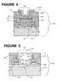
- FIGS. 4 and 5Two illustrations of using the platinum:ruthenium alloy layer or layers as described above are shown and described below with reference to FIGS. 4 and 5.
- the use of the platinum:ruthenium layer or layers according to the present inventionis described with reference to FIG. 4 wherein a bottom electrode of a high dielectric capacitor of a storage cell includes one or more layers of the platinum:ruthenium alloy material as described herein.
- FIG. 5the use of platinum:ruthenium alloy layer or layers according to the present invention is described with reference to FIG. 5 wherein a contact liner requiring difflusion barrier characteristics is described.
- FIG. 5Two illustrations of using the platinum:ruthenium alloy layer or layers as described above are shown and described below with reference to FIGS. 4 and 5.
- the use of the platinum:ruthenium layer or layers according to the present inventionis described with reference to FIG. 4 wherein a bottom electrode of a high dielectric capacitor of a storage cell includes one or more layers of the platinum:ruthenium alloy material as described herein.
- FIG. 5the
- CMOS devicesmemory devices, logic devices, etc.
- the platinum:ruthenium alloy barrier layermay be used for any application requiring diffusion barrier characteristics, particularly those for preventing diffusion of oxygen and silicon into adjacent layers.
- a device structure 100is fabricated in accordance with conventional processing techniques through the formation of an opening 184 prior to depositing a bottom electrode structure on the surfaces 185 , 186 defining the opening 184 .
- a platinum:ruthenium alloy bottom electrodeis then formed in opening 184 .
- the device structure 100includes field oxide regions 105 and active regions, i.e., those regions of the substrate 107 not covered by field oxide.
- a word line 121 and an active device, i.e., field effect transistor (FET) 122are formed relative to the field oxide region 105 .
- Suitable source/drain regions 125 , 130are created in silicon substrate 107 .
- An insulative layer of oxide material 140is formed over regions of FET 122 and word line 121 .
- Polysilicon plug 165is formed to provide electrical communication between substrate 107 and the storage cell capacitor to be formed thereover.
- Various layersare formed over the polysilicon plug 165 , including layers 167 and 175 .
- such layersmay be titanium nitride, tungsten nitride, or any other metal nitride which acts as a barrier, and may also include one or more platinum:ruthenium alloy barrier layers as described herein.
- another insulative layer 183is formed and an opening 184 is defined therein.
- the opening 184is a small high aspect ratio opening.
- small high aspect ratio openingshave feature sizes or critical dimensions below about 1 micron (e.g., such as a diameter or width of an opening being less than about 1 micron) and aspect ratios greater than about 1.
- Such aspect ratiosare applicable to contact holes, vias, trenches, and any other configured openings.
- a trench having an opening of 1 micron and depth of 3 micronshas an aspect ratio of 3.
- the present inventionis particularly beneficial for forming diffusion barrier layers in small high aspect ratio features due to the use of CVD processes for forming conformal layers of the platinum:ruthenium alloy material over step structures.
- a platinum:ruthenium alloy barrier layer 187is formed on the bottom surface 185 and the one or more side walls 186 defining opening 184 .
- a layer of platinum:ruthenium alloy materialis first co-deposited over the entire structure including the bottom surface 185 and sidewalls 186 and then formed into lower electrode 187 .
- the layermay be etched or planarized to remove the desired regions for forming the bottom electrode 187 .
- dielectric layer 191is then formed relative to the platinum:ruthenium alloy diffusion barrier layer 187 .
- the second electrode 192is formed relative to the dielectric material 191 .
- such an electrodemay be of any conductive material such as the platinum:ruthenium alloy barrier material as described herein, tungsten nitride, titanium nitride, tantalum nitride, ruthenium, rhodium, iridium, ruthenium oxide, iridium oxide, any combination thereof, or any other conductive material typically used as an electrode of a storage cell capacitor.
- the bottom electrode formed of platinum:ruthenium alloy materialis conformally formed of uniform thickness using CVD within opening 184 providing a desired resistivity and barrier properties.
- container capacitorstypically includes electrodes formed on surfaces requiring conformal formation of a bottom electrode.
- a container capacitor storage cellis described in U.S. Pat. No. 5,270,241 to Dennison, et al., entitled “Optimized Container Stack Capacitor DRAM Cell Utilizing Sacrificial Oxide Deposition and Chemical Mechanical Polishing,” issued Dec. 14, 1993.
- the bottom electrode 187may include a stack of layers with one or more of the layers being a platinum:ruthenium alloy barrier layer as described previously herein.
- device structure 200is fabricated in accordance with conventional processing techniques through the formation of contact opening 259 prior to metalization of the contact area 255 of substrate 207 .
- the device structure 200prior to metalization, includes field oxide regions 205 and active areas, i.e., those regions of substrate 207 not covered by field oxide. Formed relative to the field oxide regions 205 in the active areas are word line 221 and FET 222 .
- doped source/drain regions 225 , 230are formed as known to one skilled in the art.
- a conformal layer of oxide material 240is formed thereover and contact opening 259 is defined therein to the contact area 255 of doped region 230 of silicon substrate 207 .
- contact opening 259for providing electrical connection to substrate region 230 .
- various materialsmay be formed in contact opening 259 , such as titanium nitride or other diffusion barrier materials.
- contact liner 285is formed of platinum:ruthenium alloy material according to the present invention on bottom surface 260 and the one or more side walls 261 defining the opening 259 .
- the platinum:ruthenium alloy layersare generally deposited over the entire substrate assembly and then planarized to form the contact liner 285 .
- a conductive material 276is formed in the contact opening for providing connection to doped region 230 of substrate 207 .
- FIGS. 6A and 6Bshow depth profiles of a co-deposited platinum:ruthenium layer before and after an oxygen anneal, respectively.
- the small lab scale reaction CVD chamberwas built by MDC Vaccuum Products Corp. (Hayward, Calif.) and the glass research bubbler is from Technical Glass Service (Boise, Id.).
- the conditions used for the co-deposition of the platinum:ruthenium layerinclude:
- Reaction Chamber Conditionspressure of 5 torr, deposition temperature of 300° C. at wafer surface.
- Oxygen Reaction Gas10 sccm.
- the depth profilewas attained by using an XPS device available under the trade designation of Phi ( ⁇ ) 5600 from Physical Electronics (Eden Prairie, Minn.).
- Sputteringwas performed with a 4 keV Argon ion beam rastored over a 3 mm area.
- the sputter time for the depth profile of FIG. 6Awas 13 minutes and the sputter time for the depth profile of FIG. 6B was 14.3 minutes.
- FIG. 6Athe co-deposited platinum:ruthenium layer deposited according to the above conditions is shown therein including at a depth of 200 ⁇ a platinum composition of about 70% and a ruthenium composition of about 15%.
- FIG. 6Bshows the co-deposited platinum:ruthenium layer after being subjected to a rapid thermal oxidation anneal at 750° C. for a period of 30 seconds.
- FIG. 6Cshows an XPS montage display showing the Si signal during profile through the platinum:ruthenium layer, after annealing in oxygen. The peak shape shows the lack of SiO 2 at the interface and only traces of Si at the surface. There appears to be no silicon diffusion or oxygen diffusion through the barrier layer and therefore, no silicon dioxide formation.
Landscapes
- Engineering & Computer Science (AREA)
- Physics & Mathematics (AREA)
- Condensed Matter Physics & Semiconductors (AREA)
- General Physics & Mathematics (AREA)
- Manufacturing & Machinery (AREA)
- Computer Hardware Design (AREA)
- Microelectronics & Electronic Packaging (AREA)
- Power Engineering (AREA)
- Semiconductor Memories (AREA)
- Chemical Vapour Deposition (AREA)
- Electrodes Of Semiconductors (AREA)
- Internal Circuitry In Semiconductor Integrated Circuit Devices (AREA)
Abstract
Description
- The present invention relates to semiconductor devices and the fabrication thereof. More particularly, the present invention pertains to diffusion barrier layers.[0001]
- In the fabrication of integrated circuits, various conductive layers are used. For example, during the formation of semiconductor devices, such as dynamic random access memories (DRAMs), static random access memories (SRAMs), ferroelectric (FE) memories, etc., conductive materials are used in the formation of storage cell capacitors and also may be used in interconnection structures, e.g., conductive layers in contact holes, vias, etc. In many applications, it is preferable that the material used provide effective diffusion barrier characteristics.[0002]
- For example, effective diffusion barrier characteristics are required for conductive materials used in the formation of storage cell capacitors of memory devices, e.g., DRAMs. As memory devices become more dense, it is necessary to decrease the size of circuit components forming such devices. One way to retain storage capacity of storage cell capacitors of the memory devices and at the same time decrease the memory device size is to increase the dielectric constant of the dielectric layer of the storage cell capacitor. Therefore, high dielectric constant materials are used in such applications interposed between two electrodes. One or more layers of various conductive materials may be used as the electrode material. However, generally, one or more of the layers of the conductive materials used for the electrodes (particularly the lower electrode of a cell capacitor) must have certain barrier properties and oxidation resistance properties. Such properties are particularly required when high dielectric constant materials are used for the dielectric layer of the storage cell capacitor because of the processes used for forming such high dielectric materials, e.g., deposition of high dielectric materials usually occurs at high temperatures (generally greater than about 500° C.) in an oxygen-containing atmosphere.[0003]
- Generally, various metals and metallic compounds, and typically notable metals such as platinum and conductive oxides such as ruthenium oxide, have been proposed as the electrodes or at least one of the layers of the electrodes for use with high dielectric constant materials. However, reliable electrical connections should generally be constructed which do not diminish the beneficial properties of the high dielectric constant materials. For platinum to function well as a bottom electrode, it must be an effective barrier to the difflusion of oxygen. This is required since any oxidation of underlying silicon upon which the capacitor is formed will result in a decreased series capacitance, thus degrading the storage capacity of the cell capacitor. Platinum, used alone as an electrode layer, is too permeable to oxygen to be used as a bottom electrode of a storage cell capacitor.[0004]
- Because of the permeability of platinum to oxygen, typically platinum is used as a layer in an electrode stack which acts as the electrode as well as a diffusion barrier for integration of capacitors directly formed on silicon. For example, as described in the article “Novel High Temperature Multilayer Electrode-Barrier Structure for High Density Ferroelectric Memories” by H. D. Bhatt, et al.,[0005]Appl. Phys. Letter,71(5), Aug. 4, 1997, the electrode barrier structure includes layers of platinum:rhodium alloy, in addition to platinum:rhodium oxide layers, to form electrodes with difflusion barrier properties. Such alloy layers are formed using physical vapor deposition (PVD) processing, e.g., reactive RF sputtering processes.
- Many storage cell capacitors are formed using high aspect ratio openings. For example, in U.S. Pat. No. 5,392,189 to Fazan, et al., entitled “Capacitor Compatible with High Dielectric Constant Materials Having Two Independent Insulative Layers and the Method for Forming Same,” issued Feb. 21, 1995, the storage cell capacitors include a lower electrode that is formed by deposition of a conductive material within a small high aspect ratio opening. Typically, sputtering does not provide a sufficiently conformal layer adequate for formation of an electrode within such a small high aspect ratio opening.[0006]
- In addition to the formation of capacitor electrodes, the formation of barrier layers for use in other applications, e.g., interconnect applications, is also desirable. For example, diffusion barriers are commonly used to prevent undesirable reactions in contact openings.[0007]
- To overcome the problems described above with respect to the use of platinum alone as an electrode material, and others which will be apparent from the detailed description below, a platinum:ruthenium diffusion barrier layer, structures incorporating such layers, and methods associated therewith are described herein.[0008]
- A method for use in the fabrication of integrated circuits according to the present invention includes providing a substrate assembly having a surface and forming a barrier layer over at least a portion of the surface. The barrier layer is formed of a platinum(x):ruthenium(1-x) alloy, where x is in the range of about 0.60 to about 0.995.[0009]
- In other embodiments of the method, preferably, x is in the range of about 0.90 to about 0.98, and more preferably, x is about 0.95. In another embodiment of the method, the barrier layer is formed by chemical vapor deposition. In yet another embodiment of the method, the portion of the surface upon which the barrier layer is formed is a silicon containing surface.[0010]
- Another method for use in the formation of a capacitor according to the present invention includes forming a first electrode on a portion of a substrate assembly. A high dielectric material is formed over at least a portion of the first electrode and a second electrode is formed over the high dielectric material. At least one of the first and second electrodes comprises a layer of a platinum:ruthenium alloy.[0011]
- In one embodiment of the method, at least one of the first electrode and second electrode includes the layer of platinum(x):ruthenium(1-x) alloy and one or more additional conductive layers.[0012]
- Another method for use in forming a storage cell including a capacitor according to the present invention is described. The method includes providing a substrate assembly including at least one active device and forming a capacitor relative to the at least one active device. The capacitor comprises at least one electrode including a barrier layer of platinum(x):ruthenium(1-x) alloy.[0013]
- A semiconductor device structure according to the present invention includes a substrate assembly including a surface and a barrier layer over at least a portion of the surface. The barrier layer is formed of a platinum(x):ruthenium(1-x) alloy, wherein x is in the range of about 0.60 to about 0.995.[0014]
- A capacitor structure according to the present invention includes a first electrode, a dielectric material on at least a portion of the first electrode, and a second electrode on the dielectric material. At least one of the first and second electrodes comprises a barrier layer of platinum(x):ruthenium(1-x) alloy.[0015]
- A memory cell structure according to the present invention includes a substrate assembly including at least one active device and a capacitor formed relative to the at least one active device. The capacitor comprises at least one electrode including a barrier layer formed of platinum(x):ruthenium(1-x) alloy.[0016]
- Another integrated circuit structure includes a substrate assembly including at least one active device and an interconnect formed relative to the at least one active device. The interconnect including a barrier layer formed of platinum(x):ruthenium(1-x) alloy.[0017]
- The present invention will be better understood from reading the following description of illustrative embodiments with reference to the attached drawings, wherein below:[0018]
- FIG. 1 shows a device structure including a platinum:ruthenium alloy layer according to the present invention.[0019]
- FIG. 2 shows a structure including a platinum:ruthenium alloy layer according to the present invention as part of a multiple conductive layer stack.[0020]
- FIG. 3 is a structure including a high dielectric capacitor including an electrode having a platinum:ruthenium alloy layer according to the present invention.[0021]
- FIG. 4 illustrates the use of a platinum:ruthenium alloy layer in a storage cell capacitor application.[0022]
- FIG. 5 illustrates the use of a platinum:ruthenium alloy layer in an interconnect application.[0023]
- FIGS.[0024]6A-6C show the results of an example wherein a layer of platinum:ruthenium alloy material is deposited. FIG. 6A shows a depth profile of the deposited platinum:ruthenium alloy layer before an oxygen anneal, FIG. 6B shows a depth profile of the deposited platinum:ruthenium alloy layer after an oxygen anneal, and FIG. 6C shows an XPS montage display showing the Si signal during profile through the platinum:ruthenium layer after annealing in oxygen.
- The present invention shall be described generally with reference to FIG. 1. Thereafter, embodiments and illustrations of applications of the present invention shall be described with reference to FIGS.[0025]2-5.
- FIG. 1 illustrates a[0026]
structure 10 including asubstrate assembly 12 and a platinum:ruthenium alloy layer 14 according to the present invention formed on asurface 13 of thesubstrate assembly 12, e.g., a silicon containing surface. Thestructure 10 is illustrative of the use of a platinum:ruthenium alloy layer for any application requiring an effective barrier layer. In other words, the platinum:ruthenium alloy layer 14 may be used in the fabrication of semiconductor devices wherever it is necessary to prevent the diffusion of one material to an adjacent material. For example, thesubstrate assembly 12 may be representative of a contact structure having an opening extending to a silicon containing surface. In such a structure, diffusion barriers are commonly used in such openings to prevent undesirable reactions, such as the reaction of a contact material, e.g, aluminum, with the silicon containing surface. - Further, for example, the platinum:ruthenium[0027]
alloy barrier layer 14 may be used in the formation of storage cell capacitors for use in semiconductor devices, e.g., memory devices. As further described herein, the platinum:rutheniumalloy barrier layer 14 may be used alone as an electrode in such storage cell capacitors or within a stack of layers forming an electrode of a capacitor. One skilled in the art will recognize that various semiconductor processes and structures for various devices, e.g., CMOS devices, memory devices, etc., would benefit from the barrier characteristics of the barrier layers of the present invention and in no manner is the present invention limited to the illustrative embodiments described herein. - As used in this application, “substrate assembly” refers to either a semiconductor substrate such as the base semiconductor layer, e.g., the lowest layer of a silicon material in a wafer, or a silicon layer deposited on another material, such as silicon on sapphire, or a semiconductor substrate having one or more layers or structures formed thereon or regions formed therein. When reference is made to a substrate assembly in the following description, various process steps may have been previously used to form or define regions, junctions, various structures or features, and openings such as vias, contact openings, high aspect ratio openings, etc.[0028]
- The platinum:[0029]
ruthenium alloy layer 14 according to the present invention, includes an atomic composition of platinum(x):ruthenium(1-x), where preferably, x is in the range of about 0.60 to about 0.995. In other words, the amount of ruthenium necessary in the platinum layer to accomplish barrier characteristics for semiconductor devices is minimal, i.e., in the range of about 40% to about 0.5%. More preferably, x is in the range of about 0.90 to about 0.98; and, yet more preferably, x is about 0.95, i.e., about 5% ruthenium in the layer is suitable to provide barrier characteristics. In other words, preferably, the atomic composition of the platinum:ruthenium alloy layer 14 is about 95% platinum and 5% ruthenium. - The thickness of the platinum:[0030]
ruthenium alloy layer 14 is dependent upon the application for which it is used. Preferably, the thickness is in the range of about 10 Å to about 10,000 Å. More preferably, the thickness of the platinum:ruthenium alloy layer 14 is in the range of about 100 Å to about 500 Å. For example, this preferred thickness range of about 100 Å to about 500 Å is applicable to a single platinum:ruthenium alloy layer forming an electrode of a capacitor. - The platinum:[0031]
ruthenium alloy layer 14 formed on thesurface 13 ofsubstrate assembly 12 may be formed by one or more various processes. For example, the formation of the platinum:ruthenium alloy layer 14 may be accomplished by the simultaneous evaporation of the metals from respective sources, i.e., co-evaporation; may be sputter deposited from a single deposition target of platinum:ruthenium alloy; may be deposited by the simultaneous co-sputtering from two targets (i.e., one target including platinum and the other target including ruthenium); or may be deposited by chemical vapor deposition (CVD), for example, atmospheric pressure chemical vapor deposition, low pressure chemical vapor deposition (LPCVD), plasma enhanced chemical vapor deposition (PECVD), or any other chemical vapor deposition technique. Preferably, the formation of the platinum:ruthenium alloy layer 14 is attained by CVD. - For example, the process may be carried out in a chemical vapor deposition reactor, such as a reaction chamber available under the trade designation of 7000 from Genus, Inc., (Sunnyvale, Calif.), or available under the trade designation of 5000 from Applied Materials, Inc., (Santa Clara, Calif.), or available under the trade designation of Prism from Novelus, Inc., (San Jose, Calif.). However, any reaction chamber suitable for performing CVD may be used.[0032]
- Chemical vapor deposition (CVD) is defined as the formation of a non-volatile solid film on a substrate by the reaction of vapor phase reactants, i.e., reactant gases, that contain desired components. The reactant gases are introduced into the reaction chamber. The gases decompose and react at a heated wafer surface to form the desired layer. Chemical vapor deposition is just one process of providing thin layers on semiconductor wafers, such as films of elemental metals or compounds, e.g., platinum:ruthenium alloy layers. Chemical vapor deposition processes are favored in many respects because of the process capability to provide highly conformal layers even within deep contacts and other openings. Thus, as described further below with reference to FIGS. 4 and 5, CVD processing is preferably used to provide highly conformal layers within deep contacts and other openings such as for lower electrodes of storage cell capacitors. It will be readily apparent to one skilled in the art that although CVD is the preferred process, that the CVD process may be enhanced by various related techniques such as plasma assistance, photo assistance, laser assistance, as well as other techniques.[0033]
- Preferably, according to the present invention, the co-deposition of platinum and ruthenium is conducted using a CVD process wherein a ruthenium precursor is delivered to a reaction chamber along with a platinum precursor. Preferably, the method is carried out in the presence of an oxidizing reactant gas, such as O[0034]2, NO, N2O, O3, hydrogen peroxide, organic peroxides such as T-butyl peroxide, or any other oxidizing agent.
- Typically, a liquid precursor is contained in a bubbler reservoir through which a carrier gas, such as helium or any other inert, i.e., nonreactive gas (e.g., nitrogen, argon, neon, and xenon) is bubbled through the reservoir containing the precursor to deliver the precursor to the reaction chamber. For example, a flow of carrier gas having a flow in the range of about one sccm to about 100 sccm of a nonreactive gas, i.e., nonreactive with other gases of the process, is used in a bubbler having a pressure in the range of about 0.5 to about 50 torr and a temperature in the range of about 30° C. to about 70° C. to deliver a platinum precursor to the reaction chamber. Likewise, a carrier gas, i.e., a nonreactive gas, having a flow in a range of about one sccm to about 10 sccm is used in a bubbler containing a ruthenium precursor at the conditions of about 0.5 torr to about 100 torr and a temperature of about 20° C. to about 50° C. to deliver the ruthenium precursor to the reaction chamber. Preferably, the reactant oxidizing gas is provided to the reaction chamber at a flow of about 0 sccm to about 500 sccm.[0035]
- One skilled in the art will recognize that the manner in which the gases are introduced into the reaction chamber may include one of various techniques. For example, in addition to provision by bubbler techniques, the introduction may be accomplished with the use of compounds which are gases at room temperature or by heating a volatile compound and delivering the volatile compound to the reaction chamber using a carrier gas. Further, solid precursors and various methods of vaporizing such solid precursors may also be used for introduction of reactant compounds into the chamber. As such, the present invention is not limited to any particular technique. Further, typically, the reactant gases are admitted at separate inlet ports. In addition to the reactant gases, a dilution gas (i.e., a gas that is non-reactive with the reactant gases) may also be introduced into the chamber. For example, argon gas may be introduced into the chamber at a varied flow rate.[0036]
- Therefore, in accordance with the present invention, the reactant gas mixture in the reaction chamber includes at least the ruthenium precursor gas, the platinum precursor gas, and optionally the oxygen reactant gas and/or a dilution gas. Preferably, within the reaction chamber, the partial pressure of ruthenium precursor gas is kept sufficiently low such that the ruthenium deposited is within the ranges described for forming the preferred platinum:ruthenium composition of the[0037]
alloy layer 14 described above. This partial pressure may be controlled by controlling the flow of the inert gas, e.g., helium, through the bubbler containing the ruthenium precursor or through control of other parameters of the process, such as temperature and pressure of the bubbler. - In the preferred CVD process, the reaction chamber pressure is preferably maintained at a deposition pressure of about 0.5 torr to about 5 torr. The deposition temperature at the wafer surface upon which the platinum:[0038]
ruthenium alloy layer 14 is deposited is held at a temperature in a range of about 200° C. to about 400° C. - Any ruthenium-containing precursor and platinum-containing precursor may be used in accordance with the present invention. Preferably, the platinum containing precursors include MeCpPtMe[0039]3(where Cp=cyclopentadienyl), platinum hexafluoroacetylacetonate, CpPtMe3, Pt(acetylacetonate)2, Pt(F3)4, Pt(CO)2Cl2, cis-PtMe2[MeNC]2, (COD)Pt(CH3)2, (COD)Pt(CH3)Cl, (C5H5)Pt(CH3)(CO), (acac)(Pt)(CH3)3, where COD=1,5 cycloctadiene and acac=acetylacetonate. Further, preferably, the ruthenium precursors are liquid ruthenium complexes of the following formula (Formula I): (diene)Ru(CO)3wherein: “diene” refers to linear, branched, or cyclic dienes, bicyclic dienes, tricyclic dienes, fluorinated derivatives thereof, combinations thereof, and derivatives thereof additionally containing heteroatoms such as halide, Si, S, Se, P, As, or N. These precursor complexes and others are described in Assignees' copending patent application entitled “Precursor Chemistries for Chemical Vapor Deposition of Ruthenium and Ruthenium Oxide” having U.S. Ser. No. ______ (Micron Docket No. 97-0675) and in Assignees' copending patent application entitled “Methods for Preparing Ruthenium and Osmium Compounds” having U.S. Ser. No. ______ (Micron Docket No. 97-0861). Further, for example, additional precursors are generally discussed in U.S. Pat. No. 5,372,849 to McCormick et al. More preferably, the ruthenium precursors used according to the present invention include one of C6H8Ru(CO)3, bis(cyclopentadienyl) ruthenium (II), triruthenium dodecacarbonyl, and cyclopentadienyl dicarbonyl ruthenium (II) dimer.
- Methods of forming the co-deposited platinum:[0040]
ruthenium alloy layer 14 are described in co-pending patent application entitled “Method for Producing Low Carbon/Oxygen Conductive Layers” (Docket No. 150.00730101 (Micron Docket No. 97-0996). One skilled in the art will recognize that these methods and various other methods may be used to form the platinum:ruthenium alloy layer 14 according to the present invention. - FIG. 2 shows a[0041]
structure 20 includingsubstrate assembly 22 and astack 24. Thestack 24 includes conductive layers31-34. One or more of the conductive layers31-34 are platinum:ruthenium alloy layers according to the present invention. - The one or more conductive layers, in addition to including one or more platinum:ruthenium alloy layers, may include conductive layers formed of various conductive materials. For example, the conductive layers may include, but are clearly not limited to, layers formed from metals such as platinum, paladium, rhodium, ruthenium, osmium, and iridium; metal alloys such as platinum:rhodium, platinum:ruthenium, and platinum:iridium; metal oxides such as ruthenium oxide, rhodium oxide, and iridium oxide; metal alloy oxides such as platinum:rhodium oxide, platinum:ruthenium oxide, and platinum:iridium oxide; metal nitrides such as titanium nitride, tungsten nitride, and tantalum nitride; metal silicides such as titanium silicide, ruthenium silicide, rhodium silicide, and iridium silicide.[0042]
- The[0043]
stack 24 may be used for one or numerous applications, e.g., interconnection applications, capacitor applications, etc. For example, stack24 may be used as an electrode for a storage cell capacitor withsubstrate assembly 22 including asilicon containing surface 23. As such, the barrier properties of thestack 24 must prevent silicon difflusion from silicon-containingsurface 23. In accordance with the present invention, the layer31 may be formed as a platinum:ruthenium alloy layer to prevent diffusion of silicon from silicon-containingsurface 23 throughstack 24 to adjacent layer or layers29. Further, for example, in the case wherelayer 29 is a high dielectric material requiring diffusion barrier properties to prevent oxygen from diffusing throughstack 24,layer 34 or one of the other layers may also be formed as a platinum:ruthenium alloy barrier layer according to the present invention. One skilled in the art will recognize that the platinum:ruthenium alloy layer according to the present invention may be used in a stack of layers for a variety of applications and the stack may include one or more platinum:ruthenium alloy layers. Further, the composition of such platinum:ruthenium layers used in the same stack may differ. - FIG. 3 shows a[0044]
structure 50 includingsubstrate assembly 52 andcapacitor structure 54.Capacitor structure 54 includes afirst electrode 56, asecond electrode 60, and a high dielectricconstant layer 58 interposed therebetween. For example, the dielectric layer may be any suitable material having a desirable dielectric constant, such as Ta2O5, BaxSr(1-X)TiO3[BST], BaTiO3, SrTiO3, PbTiO3, Pb(Zr,Ti)O3[PZT], (Pb,La)(Zr,Ti)O3[PLZT], (Pb,La)TiO3[PLT], KNO3, and LiNbO3. With use of the high dielectricconstant layer 58, diffusion barrier properties of the electrodes is particularly important. For example, to function well in a bottom electrode of a capacitor structure, the electrode layer or electrode stack must act as an effective barrier to the diffusion of oxygen, particularly due to the processes used to form the high dielectric constant materials. Such diffusion barrier properties are particularly required when thesubstrate assembly 52 includes a silicon-containingsurface 53 upon which the capacitor is formed, e.g., polysilicon, silicon substrate material, N-doped silicon, P-doped silicon, etc., since oxidation of the diffused silicon may result in degraded capacitance, e.g., capacitance for a memory device. The co-deposition of the platinum with the ruthenium enhances the barrier properties of the layer formed and thus provides a significant improvement over pure platinum for electrode applications. - One skilled in the art will recognize that either of the[0045]
electrodes such electrodes - Two illustrations of using the platinum:ruthenium alloy layer or layers as described above are shown and described below with reference to FIGS. 4 and 5. The use of the platinum:ruthenium layer or layers according to the present invention is described with reference to FIG. 4 wherein a bottom electrode of a high dielectric capacitor of a storage cell includes one or more layers of the platinum:ruthenium alloy material as described herein. Further, the use of platinum:ruthenium alloy layer or layers according to the present invention is described with reference to FIG. 5 wherein a contact liner requiring difflusion barrier characteristics is described. For simplistic purposes, the illustrative descriptions are limited to the use of the platinum:ruthenium alloy material described in these two illustrative structures. There are other semiconductor processes and structures for various devices, e.g., CMOS devices, memory devices, logic devices, etc., that would benefit from the present invention and in no manner is the present invention limited to the illustrative embodiments described herein, e.g., contact liner and electrode structure. The platinum:ruthenium alloy barrier layer may be used for any application requiring diffusion barrier characteristics, particularly those for preventing diffusion of oxygen and silicon into adjacent layers.[0046]
- As shown in FIG. 4, a[0047]
device structure 100 is fabricated in accordance with conventional processing techniques through the formation of anopening 184 prior to depositing a bottom electrode structure on thesurfaces opening 184. A platinum:ruthenium alloy bottom electrode is then formed inopening 184. As such, and as further described in U.S. Pat. No. 5,392,189 to Fazan, et al., thedevice structure 100 includesfield oxide regions 105 and active regions, i.e., those regions of thesubstrate 107 not covered by field oxide. Aword line 121 and an active device, i.e., field effect transistor (FET)122, are formed relative to thefield oxide region 105. Suitable source/drain regions silicon substrate 107. An insulative layer ofoxide material 140 is formed over regions ofFET 122 andword line 121.Polysilicon plug 165 is formed to provide electrical communication betweensubstrate 107 and the storage cell capacitor to be formed thereover. Various layers are formed over thepolysilicon plug 165, includinglayers 167 and175. For example, such layers may be titanium nitride, tungsten nitride, or any other metal nitride which acts as a barrier, and may also include one or more platinum:ruthenium alloy barrier layers as described herein. Thereafter, anotherinsulative layer 183 is formed and anopening 184 is defined therein. - The[0048]
opening 184 is a small high aspect ratio opening. As described herein, small high aspect ratio openings have feature sizes or critical dimensions below about 1 micron (e.g., such as a diameter or width of an opening being less than about 1 micron) and aspect ratios greater than about 1. Such aspect ratios are applicable to contact holes, vias, trenches, and any other configured openings. For example, a trench having an opening of 1 micron and depth of 3 microns has an aspect ratio of 3. The present invention is particularly beneficial for forming diffusion barrier layers in small high aspect ratio features due to the use of CVD processes for forming conformal layers of the platinum:ruthenium alloy material over step structures. - As shown in FIG. 4, a platinum:ruthenium[0049]
alloy barrier layer 187 is formed on thebottom surface 185 and the one ormore side walls 186 definingopening 184. A layer of platinum:ruthenium alloy material is first co-deposited over the entire structure including thebottom surface 185 andsidewalls 186 and then formed intolower electrode 187. For example, the layer may be etched or planarized to remove the desired regions for forming thebottom electrode 187. Thereafter,dielectric layer 191 is then formed relative to the platinum:ruthenium alloydiffusion barrier layer 187. Further thereafter, thesecond electrode 192 is formed relative to thedielectric material 191. For example, such an electrode may be of any conductive material such as the platinum:ruthenium alloy barrier material as described herein, tungsten nitride, titanium nitride, tantalum nitride, ruthenium, rhodium, iridium, ruthenium oxide, iridium oxide, any combination thereof, or any other conductive material typically used as an electrode of a storage cell capacitor. With the use of the present invention, the bottom electrode formed of platinum:ruthenium alloy material is conformally formed of uniform thickness using CVD withinopening 184 providing a desired resistivity and barrier properties. - It will be recognized by one skilled in the art that any capacitor formed relative to a surface, e.g., silicon containing surface, whereupon diffusion barrier properties are required and/or conformally formed conductive layers are required will benefit from the present invention. For example, container capacitors typically includes electrodes formed on surfaces requiring conformal formation of a bottom electrode. Such a container capacitor storage cell is described in U.S. Pat. No. 5,270,241 to Dennison, et al., entitled “Optimized Container Stack Capacitor DRAM Cell Utilizing Sacrificial Oxide Deposition and Chemical Mechanical Polishing,” issued Dec. 14, 1993. One skilled in the art will also recognize that the[0050]
bottom electrode 187 may include a stack of layers with one or more of the layers being a platinum:ruthenium alloy barrier layer as described previously herein. - As shown in FIG. 5,[0051]
device structure 200 is fabricated in accordance with conventional processing techniques through the formation ofcontact opening 259 prior to metalization of thecontact area 255 ofsubstrate 207. As such, prior to metalization, thedevice structure 200 includesfield oxide regions 205 and active areas, i.e., those regions ofsubstrate 207 not covered by field oxide. Formed relative to thefield oxide regions 205 in the active areas areword line 221 andFET 222. Suitably doped source/drain regions oxide material 240 is formed thereover andcontact opening 259 is defined therein to thecontact area 255 of dopedregion 230 ofsilicon substrate 207. Thereafter, one or more metalization or conductive layers are formed in thecontact opening 259 for providing electrical connection tosubstrate region 230. For example, various materials may be formed incontact opening 259, such as titanium nitride or other diffusion barrier materials. Preferably,contact liner 285 is formed of platinum:ruthenium alloy material according to the present invention onbottom surface 260 and the one ormore side walls 261 defining theopening 259. The platinum:ruthenium alloy layers are generally deposited over the entire substrate assembly and then planarized to form thecontact liner 285. Thereafter, aconductive material 276 is formed in the contact opening for providing connection to dopedregion 230 ofsubstrate 207. - FIGS. 6A and 6B show depth profiles of a co-deposited platinum:ruthenium layer before and after an oxygen anneal, respectively. The small lab scale reaction CVD chamber was built by MDC Vaccuum Products Corp. (Hayward, Calif.) and the glass research bubbler is from Technical Glass Service (Boise, Id.). The conditions used for the co-deposition of the platinum:ruthenium layer include:[0052]
- Platinum Precursor: MeCpPt(Me)[0053]3.
- Ruthenium Precursor: C[0054]6H8Ru(CO)3.
- Platinum Carrier Gas for use through Bubbler: 5 sccm of helium.[0055]
- Ruthenium Carrier Gas for use through Bubbler: 10 sccm of helium.[0056]
- Platinum Bubbler Conditions: pressure of 10 torr, temperature of 33° C.[0057]
- Ruthenium Bubbler Conditions: pressure of 40 torr, temperature of 25° C.[0058]
- Reaction Chamber Conditions: pressure of 5 torr, deposition temperature of 300° C. at wafer surface.[0059]
- Deposition Time: 4 minutes.[0060]
- Oxygen Reaction Gas: 10 sccm.[0061]
- The depth profile was attained by using an XPS device available under the trade designation of Phi (Φ) 5600 from Physical Electronics (Eden Prairie, Minn.). The operating conditions for obtaining the profile include x-ray source of 350 W, monochromatic Al k[0062]α (hV=1486.6 eV); 45 degree extraction; 800 μm extraction aperture. Sputtering was performed with a 4 keV Argon ion beam rastored over a 3 mm area. The sputter time for the depth profile of FIG. 6A was 13 minutes and the sputter time for the depth profile of FIG. 6B was 14.3 minutes.
- As shown in FIG. 6A, the co-deposited platinum:ruthenium layer deposited according to the above conditions is shown therein including at a depth of 200 Å a platinum composition of about 70% and a ruthenium composition of about 15%. FIG. 6B shows the co-deposited platinum:ruthenium layer after being subjected to a rapid thermal oxidation anneal at 750° C. for a period of 30 seconds. FIG. 6C shows an XPS montage display showing the Si signal during profile through the platinum:ruthenium layer, after annealing in oxygen. The peak shape shows the lack of SiO[0063]2at the interface and only traces of Si at the surface. There appears to be no silicon diffusion or oxygen diffusion through the barrier layer and therefore, no silicon dioxide formation.
- All patents and references cited herein are incorporated in their entirety as if each were incorporated separately. This invention has been described with reference to illustrative embodiments and is not meant to be construed in a limiting sense. As described previously, one skilled in the art will recognize that various other illustrative applications may use the platinum:ruthenium alloy layer as described herein to take advantage of the beneficial barrier characteristics thereof. Various modifications of the illustrative embodiments, as well as additional to the invention, will be apparent to persons skilled in the art upon reference to this description. It is therefore contemplated that the appended claims will cover any such modifications or embodiments that may fall within the scope of the present invention as defined by the accompanying claims.[0064]
Claims (39)
1. A method for use in the fabrication of integrated circuits, the method comprising:
providing a substrate assembly having a surface; and
forming a barrier layer over the at least a portion of the surface, wherein the barrier layer is formed of a platinum(x):ruthenium(1-x) alloy, where x is in the range of about 0.60 to about 0.995.
2. The method ofclaim 1 , wherein x is in the range of about 0.90 to about 0.98.
3. The method ofclaim 2 , wherein x is about 0.95.
4. The method ofclaim 1 , wherein forming the barrier layer includes forming the barrier layer by chemical vapor deposition.
5. The method ofclaim 1 , wherein the portion of the surface is a silicon containing surface.
6. A method for use in the formation of a capacitor, the method comprising:
forming a first electrode on a portion of a substrate assembly;
forming a high dielectric material over at least a portion of the first electrode;
and
forming a second electrode over the high dielectric material, wherein at least one of the first and second electrodes comprises a layer of a platinum:ruthenium alloy.
7. The method ofclaim 6 , wherein the layer of platinum:ruthenium alloy is a layer of a platinum(x):ruthenium(1-x) alloy, where x is in the range of about 0.60 to about 0.995.
8. The method ofclaim 7 , wherein x is in the range of about 0.90 to about 0.98.
9. The method ofclaim 8 , wherein x is about 0.95.
10. The method ofclaim 1 , wherein forming the at least one of the first electrode and second electrode comprising the layer of platinum(x):ruthenium(1-x) alloy includes forming the layer of platinum(x):ruthenium(1-x) alloy by chemical vapor deposition.
11. A method for use in the formation of a capacitor, the method comprising:
providing a silicon containing surface of a substrate assembly;
forming a first electrode on a least a portion of the silicon containing surface of the substrate assembly, the first electrode including a layer of platinum(x):ruthenium(1-x) alloy;
providing a high dielectric material over at least a portion of the first electrode; and
providing a second electrode over the high dielectric material.
12. The method ofclaim 11 , wherein the first electrode is a single layer of platinum (x) and ruthenium (1-x) alloy.
13. The method ofclaim 12 , wherein a thickness of the layer is in a range of about 100 Å to about 500 Å.
14. The method ofclaim 11 , wherein the step of forming the first electrode includes depositing the layer of platinum (x):ruthenium (1-x) alloy by chemical vapor deposition.
15. The method ofclaim 11 , wherein x is in the range of about 0.60 to about 0.995.
16. The method ofclaim 15 , wherein x is in the range of about 0.90 to about 0.98.
17. The method ofclaim 11 , wherein the first electrode includes the layer of platinum(x):ruthenium(1-x) alloy and one or more additional conductive layers.
18. The method ofclaim 17 , wherein the one or more additional conductive layers are formed from materials selected from the group of metals and metal alloys; metal and metal alloy oxides; metal nitrides; and metal silicides.
19. A method for use in forming a storage cell including a capacitor, the method comprising:
providing a substrate assembly including at least one active device; and
forming a capacitor relative to the at least one active device, the capacitor comprising at least one electrode including a barrier layer of platinum(x):ruthenium(1-x) alloy.
20. The method ofclaim 19 , wherein forming the at least one electrode includes depositing the barrier layer of platinum (x):ruthenium(1-x) alloy by chemical vapor deposition.
21. The method ofclaim 19 , wherein x is in the range of about 0.60 to about 0.995.
22. The method ofclaim 21 , wherein x is in the range of about 0.90 to about 0.98.
23. A semiconductor device structure, the structure comprising:
a substrate assembly including a surface; and
a barrier layer over at least a portion of the surface, wherein the barrier layer is formed of a platinum(x):ruthenium(1-x) alloy, where x is in the range of about 0.60 to about 0.995.
24. The structure ofclaim 23 , wherein x is in the range of about 0.90 to about 0.98.
25. The structure ofclaim 24 , wherein x is about 0.95.
26. The structure ofclaim 23 , wherein the portion of the surface is a silicon containing surface.
27. A capacitor structure comprising:
a first electrode;
a dielectric material on at least a portion of the first electrode; and
a second electrode on the dielectric material, wherein at least one of the first and second electrode comprises a barrier layer of platinum(x):ruthenium(1-x) alloy.
28. The structure ofclaim 27 , wherein x is in the range of about 0.60 to about 0.995.
29. The structure ofclaim 28 , wherein x is in the range of about 0.90 to about 0.98.
30. The structure ofclaim 27 , wherein at least one of the first electrode and second electrode comprises the barrier layer of platinum(x):ruthenium(1-x) alloy and one or more additional conductive layers.
31. The structure ofclaim 30 , wherein the one or more additional conductive layers are formed from materials selected from materials selected from the group of metals and metal alloys; metal and metal alloy oxides; metal nitrides; and metal silicides.
32. A memory cell structure comprising:
a substrate assembly including at least one active device; and
a capacitor formed relative to the at least one active device, the capacitor comprising at least one electrode including a barrier layer formed of platinum(x):ruthenium(1-x) alloy.
33. The structure ofclaim 32 , wherein the capacitor includes:
a first electrode formed relative to a silicon containing region of the at least one active device;
a dielectric material on at least a portion of the first electrode; and
a second electrode on the dielectric material, wherein the first electrode comprises the barrier layer formed of platinum(x):ruthenium(1-x) alloy.
34. The structure ofclaim 33 , wherein the first electrode comprising the barrier layer formed of platinum(x):ruthenium(1-x) alloy includes one or more additional conductive layers.
35. The structure ofclaim 33 , wherein x is in the range of about 0.60 to about 0.995.
36. The structure ofclaim 35 , wherein x is in the range of about 0.90 to about 0.98.
37. A integrated circuit structure comprising:
a substrate assembly including at least one active device; and
an interconnect formed relative to the at least one active device, the interconnect including a barrier layer formed of platinum(x):ruthenium(1-x) alloy.
38. The structure ofclaim 37 , wherein x is in the range of about 0.60 to about 0.995.
39. The structure ofclaim 38 , wherein x is in the range of about 0.90 to about 0.98.
Priority Applications (1)
| Application Number | Priority Date | Filing Date | Title |
|---|---|---|---|
| US09/942,200US20020008270A1 (en) | 1998-09-03 | 2001-08-29 | Diffusion barrier layers and methods of forming same |
Applications Claiming Priority (2)
| Application Number | Priority Date | Filing Date | Title |
|---|---|---|---|
| US09/146,866US6323081B1 (en) | 1998-09-03 | 1998-09-03 | Diffusion barrier layers and methods of forming same |
| US09/942,200US20020008270A1 (en) | 1998-09-03 | 2001-08-29 | Diffusion barrier layers and methods of forming same |
Related Parent Applications (1)
| Application Number | Title | Priority Date | Filing Date |
|---|---|---|---|
| US09/146,866DivisionUS6323081B1 (en) | 1998-09-03 | 1998-09-03 | Diffusion barrier layers and methods of forming same |
Publications (1)
| Publication Number | Publication Date |
|---|---|
| US20020008270A1true US20020008270A1 (en) | 2002-01-24 |
Family
ID=22519319
Family Applications (2)
| Application Number | Title | Priority Date | Filing Date |
|---|---|---|---|
| US09/146,866Expired - LifetimeUS6323081B1 (en) | 1998-09-03 | 1998-09-03 | Diffusion barrier layers and methods of forming same |
| US09/942,200AbandonedUS20020008270A1 (en) | 1998-09-03 | 2001-08-29 | Diffusion barrier layers and methods of forming same |
Family Applications Before (1)
| Application Number | Title | Priority Date | Filing Date |
|---|---|---|---|
| US09/146,866Expired - LifetimeUS6323081B1 (en) | 1998-09-03 | 1998-09-03 | Diffusion barrier layers and methods of forming same |
Country Status (5)
| Country | Link |
|---|---|
| US (2) | US6323081B1 (en) |
| JP (2) | JP5328065B2 (en) |
| KR (1) | KR100441190B1 (en) |
| AU (1) | AU5799699A (en) |
| WO (1) | WO2000014778A1 (en) |
Cited By (330)
| Publication number | Priority date | Publication date | Assignee | Title |
|---|---|---|---|---|
| US20040043580A1 (en)* | 2002-08-29 | 2004-03-04 | Micron Technology, Inc. | Protection in integrated circuits |
| US20040048467A1 (en)* | 2000-08-31 | 2004-03-11 | Micron Technologies, Inc. | Devices containing platinum-iridium films and methods of preparing such films and devices |
| US20040147086A1 (en)* | 1998-08-26 | 2004-07-29 | Micron Technology, Inc. | Methods and apparatus for forming rhodium-containing layers |
| US20080310231A1 (en)* | 2003-12-05 | 2008-12-18 | Cleeves James M | Optimization of critical dimensions and pitch of patterned features in and above a substrate |
| US7560815B1 (en) | 1998-08-27 | 2009-07-14 | Micron Technology, Inc. | Device structures including ruthenium silicide diffusion barrier layers |
| US20100025854A1 (en)* | 2008-08-04 | 2010-02-04 | Micron Technology, Inc. | Polishing systems and methods for removing conductive material from microelectronic substrates |
| US20100255653A1 (en)* | 2009-04-07 | 2010-10-07 | Micron Technology, Inc. | Semiconductor processing |
| US20110204427A1 (en)* | 2010-02-25 | 2011-08-25 | Samsung Electronics Co., Ltd. | Capacitor having an electrode structure, method of manufacturing a capacitor having an electrode structure and semiconductor device having an electrode structure |
| US20120112349A1 (en)* | 2010-11-04 | 2012-05-10 | Hynix Semiconductor Inc. | Semiconductor device |
| US20130168812A1 (en)* | 2012-01-04 | 2013-07-04 | Inotera Memories, Inc. | Memory capacitor having a robust moat and manufacturing method thereof |
| US20130221420A1 (en)* | 2000-11-10 | 2013-08-29 | Micron Technology, Inc. | Structure comprising a ruthenium metal material |
| WO2019158960A1 (en)* | 2018-02-14 | 2019-08-22 | Asm Ip Holding B.V. | A method for depositing a ruthenium-containing film on a substrate by a cyclical deposition process |
| US10559458B1 (en) | 2018-11-26 | 2020-02-11 | Asm Ip Holding B.V. | Method of forming oxynitride film |
| US10561975B2 (en) | 2014-10-07 | 2020-02-18 | Asm Ip Holdings B.V. | Variable conductance gas distribution apparatus and method |
| USD876504S1 (en) | 2017-04-03 | 2020-02-25 | Asm Ip Holding B.V. | Exhaust flow control ring for semiconductor deposition apparatus |
| US10590535B2 (en) | 2017-07-26 | 2020-03-17 | Asm Ip Holdings B.V. | Chemical treatment, deposition and/or infiltration apparatus and method for using the same |
| US10600673B2 (en) | 2015-07-07 | 2020-03-24 | Asm Ip Holding B.V. | Magnetic susceptor to baseplate seal |
| US10604847B2 (en) | 2014-03-18 | 2020-03-31 | Asm Ip Holding B.V. | Gas distribution system, reactor including the system, and methods of using the same |
| US10612136B2 (en) | 2018-06-29 | 2020-04-07 | ASM IP Holding, B.V. | Temperature-controlled flange and reactor system including same |
| US10622375B2 (en) | 2016-11-07 | 2020-04-14 | Asm Ip Holding B.V. | Method of processing a substrate and a device manufactured by using the method |
| US10643904B2 (en) | 2016-11-01 | 2020-05-05 | Asm Ip Holdings B.V. | Methods for forming a semiconductor device and related semiconductor device structures |
| US10643826B2 (en) | 2016-10-26 | 2020-05-05 | Asm Ip Holdings B.V. | Methods for thermally calibrating reaction chambers |
| US10655221B2 (en) | 2017-02-09 | 2020-05-19 | Asm Ip Holding B.V. | Method for depositing oxide film by thermal ALD and PEALD |
| US10658205B2 (en) | 2017-09-28 | 2020-05-19 | Asm Ip Holdings B.V. | Chemical dispensing apparatus and methods for dispensing a chemical to a reaction chamber |
| US10658181B2 (en) | 2018-02-20 | 2020-05-19 | Asm Ip Holding B.V. | Method of spacer-defined direct patterning in semiconductor fabrication |
| US10665452B2 (en) | 2016-05-02 | 2020-05-26 | Asm Ip Holdings B.V. | Source/drain performance through conformal solid state doping |
| US10672636B2 (en) | 2017-08-09 | 2020-06-02 | Asm Ip Holding B.V. | Cassette holder assembly for a substrate cassette and holding member for use in such assembly |
| US10683571B2 (en) | 2014-02-25 | 2020-06-16 | Asm Ip Holding B.V. | Gas supply manifold and method of supplying gases to chamber using same |
| US10685834B2 (en) | 2017-07-05 | 2020-06-16 | Asm Ip Holdings B.V. | Methods for forming a silicon germanium tin layer and related semiconductor device structures |
| US10692741B2 (en) | 2017-08-08 | 2020-06-23 | Asm Ip Holdings B.V. | Radiation shield |
| US10707106B2 (en) | 2011-06-06 | 2020-07-07 | Asm Ip Holding B.V. | High-throughput semiconductor-processing apparatus equipped with multiple dual-chamber modules |
| US10714335B2 (en) | 2017-04-25 | 2020-07-14 | Asm Ip Holding B.V. | Method of depositing thin film and method of manufacturing semiconductor device |
| US10714350B2 (en) | 2016-11-01 | 2020-07-14 | ASM IP Holdings, B.V. | Methods for forming a transition metal niobium nitride film on a substrate by atomic layer deposition and related semiconductor device structures |
| US10714315B2 (en) | 2012-10-12 | 2020-07-14 | Asm Ip Holdings B.V. | Semiconductor reaction chamber showerhead |
| US10714385B2 (en) | 2016-07-19 | 2020-07-14 | Asm Ip Holding B.V. | Selective deposition of tungsten |
| US10720322B2 (en) | 2016-02-19 | 2020-07-21 | Asm Ip Holding B.V. | Method for forming silicon nitride film selectively on top surface |
| US10720331B2 (en) | 2016-11-01 | 2020-07-21 | ASM IP Holdings, B.V. | Methods for forming a transition metal nitride film on a substrate by atomic layer deposition and related semiconductor device structures |
| US10734223B2 (en) | 2017-10-10 | 2020-08-04 | Asm Ip Holding B.V. | Method for depositing a metal chalcogenide on a substrate by cyclical deposition |
| US10734244B2 (en) | 2017-11-16 | 2020-08-04 | Asm Ip Holding B.V. | Method of processing a substrate and a device manufactured by the same |
| US10731249B2 (en) | 2018-02-15 | 2020-08-04 | Asm Ip Holding B.V. | Method of forming a transition metal containing film on a substrate by a cyclical deposition process, a method for supplying a transition metal halide compound to a reaction chamber, and related vapor deposition apparatus |
| US10734497B2 (en) | 2017-07-18 | 2020-08-04 | Asm Ip Holding B.V. | Methods for forming a semiconductor device structure and related semiconductor device structures |
| US10741385B2 (en) | 2016-07-28 | 2020-08-11 | Asm Ip Holding B.V. | Method and apparatus for filling a gap |
| US10755922B2 (en) | 2018-07-03 | 2020-08-25 | Asm Ip Holding B.V. | Method for depositing silicon-free carbon-containing film as gap-fill layer by pulse plasma-assisted deposition |
| US10755923B2 (en) | 2018-07-03 | 2020-08-25 | Asm Ip Holding B.V. | Method for depositing silicon-free carbon-containing film as gap-fill layer by pulse plasma-assisted deposition |
| US10770336B2 (en) | 2017-08-08 | 2020-09-08 | Asm Ip Holding B.V. | Substrate lift mechanism and reactor including same |
| US10767789B2 (en) | 2018-07-16 | 2020-09-08 | Asm Ip Holding B.V. | Diaphragm valves, valve components, and methods for forming valve components |
| US10770286B2 (en) | 2017-05-08 | 2020-09-08 | Asm Ip Holdings B.V. | Methods for selectively forming a silicon nitride film on a substrate and related semiconductor device structures |
| US10784102B2 (en) | 2016-12-22 | 2020-09-22 | Asm Ip Holding B.V. | Method of forming a structure on a substrate |
| US10787741B2 (en) | 2014-08-21 | 2020-09-29 | Asm Ip Holding B.V. | Method and system for in situ formation of gas-phase compounds |
| US10797133B2 (en) | 2018-06-21 | 2020-10-06 | Asm Ip Holding B.V. | Method for depositing a phosphorus doped silicon arsenide film and related semiconductor device structures |
| US10804098B2 (en) | 2009-08-14 | 2020-10-13 | Asm Ip Holding B.V. | Systems and methods for thin-film deposition of metal oxides using excited nitrogen-oxygen species |
| US10811256B2 (en) | 2018-10-16 | 2020-10-20 | Asm Ip Holding B.V. | Method for etching a carbon-containing feature |
| USD900036S1 (en) | 2017-08-24 | 2020-10-27 | Asm Ip Holding B.V. | Heater electrical connector and adapter |
| US10818758B2 (en) | 2018-11-16 | 2020-10-27 | Asm Ip Holding B.V. | Methods for forming a metal silicate film on a substrate in a reaction chamber and related semiconductor device structures |
| US10829852B2 (en) | 2018-08-16 | 2020-11-10 | Asm Ip Holding B.V. | Gas distribution device for a wafer processing apparatus |
| US10832903B2 (en) | 2011-10-28 | 2020-11-10 | Asm Ip Holding B.V. | Process feed management for semiconductor substrate processing |
| US10847371B2 (en) | 2018-03-27 | 2020-11-24 | Asm Ip Holding B.V. | Method of forming an electrode on a substrate and a semiconductor device structure including an electrode |
| US10847365B2 (en) | 2018-10-11 | 2020-11-24 | Asm Ip Holding B.V. | Method of forming conformal silicon carbide film by cyclic CVD |
| US10844486B2 (en) | 2009-04-06 | 2020-11-24 | Asm Ip Holding B.V. | Semiconductor processing reactor and components thereof |
| US10844484B2 (en) | 2017-09-22 | 2020-11-24 | Asm Ip Holding B.V. | Apparatus for dispensing a vapor phase reactant to a reaction chamber and related methods |
| US10847366B2 (en) | 2018-11-16 | 2020-11-24 | Asm Ip Holding B.V. | Methods for depositing a transition metal chalcogenide film on a substrate by a cyclical deposition process |
| USD903477S1 (en) | 2018-01-24 | 2020-12-01 | Asm Ip Holdings B.V. | Metal clamp |
| US10854498B2 (en) | 2011-07-15 | 2020-12-01 | Asm Ip Holding B.V. | Wafer-supporting device and method for producing same |
| US10851456B2 (en) | 2016-04-21 | 2020-12-01 | Asm Ip Holding B.V. | Deposition of metal borides |
| US10858737B2 (en) | 2014-07-28 | 2020-12-08 | Asm Ip Holding B.V. | Showerhead assembly and components thereof |
| US10865475B2 (en) | 2016-04-21 | 2020-12-15 | Asm Ip Holding B.V. | Deposition of metal borides and silicides |
| US10867788B2 (en) | 2016-12-28 | 2020-12-15 | Asm Ip Holding B.V. | Method of forming a structure on a substrate |
| US10867786B2 (en) | 2018-03-30 | 2020-12-15 | Asm Ip Holding B.V. | Substrate processing method |
| US10872771B2 (en) | 2018-01-16 | 2020-12-22 | Asm Ip Holding B. V. | Method for depositing a material film on a substrate within a reaction chamber by a cyclical deposition process and related device structures |
| US10883175B2 (en) | 2018-08-09 | 2021-01-05 | Asm Ip Holding B.V. | Vertical furnace for processing substrates and a liner for use therein |
| US10892156B2 (en) | 2017-05-08 | 2021-01-12 | Asm Ip Holding B.V. | Methods for forming a silicon nitride film on a substrate and related semiconductor device structures |
| US10896820B2 (en) | 2018-02-14 | 2021-01-19 | Asm Ip Holding B.V. | Method for depositing a ruthenium-containing film on a substrate by a cyclical deposition process |
| US10910262B2 (en) | 2017-11-16 | 2021-02-02 | Asm Ip Holding B.V. | Method of selectively depositing a capping layer structure on a semiconductor device structure |
| US10914004B2 (en) | 2018-06-29 | 2021-02-09 | Asm Ip Holding B.V. | Thin-film deposition method and manufacturing method of semiconductor device |
| US10923344B2 (en) | 2017-10-30 | 2021-02-16 | Asm Ip Holding B.V. | Methods for forming a semiconductor structure and related semiconductor structures |
| US10928731B2 (en) | 2017-09-21 | 2021-02-23 | Asm Ip Holding B.V. | Method of sequential infiltration synthesis treatment of infiltrateable material and structures and devices formed using same |
| US10934619B2 (en) | 2016-11-15 | 2021-03-02 | Asm Ip Holding B.V. | Gas supply unit and substrate processing apparatus including the gas supply unit |
| US10941490B2 (en) | 2014-10-07 | 2021-03-09 | Asm Ip Holding B.V. | Multiple temperature range susceptor, assembly, reactor and system including the susceptor, and methods of using the same |
| USD913980S1 (en) | 2018-02-01 | 2021-03-23 | Asm Ip Holding B.V. | Gas supply plate for semiconductor manufacturing apparatus |
| US10975470B2 (en) | 2018-02-23 | 2021-04-13 | Asm Ip Holding B.V. | Apparatus for detecting or monitoring for a chemical precursor in a high temperature environment |
| US11001925B2 (en) | 2016-12-19 | 2021-05-11 | Asm Ip Holding B.V. | Substrate processing apparatus |
| US11004977B2 (en) | 2017-07-19 | 2021-05-11 | Asm Ip Holding B.V. | Method for depositing a group IV semiconductor and related semiconductor device structures |
| US11015245B2 (en) | 2014-03-19 | 2021-05-25 | Asm Ip Holding B.V. | Gas-phase reactor and system having exhaust plenum and components thereof |
| US11018002B2 (en) | 2017-07-19 | 2021-05-25 | Asm Ip Holding B.V. | Method for selectively depositing a Group IV semiconductor and related semiconductor device structures |
| US11018047B2 (en) | 2018-01-25 | 2021-05-25 | Asm Ip Holding B.V. | Hybrid lift pin |
| US11022879B2 (en) | 2017-11-24 | 2021-06-01 | Asm Ip Holding B.V. | Method of forming an enhanced unexposed photoresist layer |
| US11024523B2 (en) | 2018-09-11 | 2021-06-01 | Asm Ip Holding B.V. | Substrate processing apparatus and method |
| US11031242B2 (en) | 2018-11-07 | 2021-06-08 | Asm Ip Holding B.V. | Methods for depositing a boron doped silicon germanium film |
| USD922229S1 (en) | 2019-06-05 | 2021-06-15 | Asm Ip Holding B.V. | Device for controlling a temperature of a gas supply unit |
| US11049751B2 (en) | 2018-09-14 | 2021-06-29 | Asm Ip Holding B.V. | Cassette supply system to store and handle cassettes and processing apparatus equipped therewith |
| US11053591B2 (en) | 2018-08-06 | 2021-07-06 | Asm Ip Holding B.V. | Multi-port gas injection system and reactor system including same |
| US11056567B2 (en) | 2018-05-11 | 2021-07-06 | Asm Ip Holding B.V. | Method of forming a doped metal carbide film on a substrate and related semiconductor device structures |
| US11056344B2 (en) | 2017-08-30 | 2021-07-06 | Asm Ip Holding B.V. | Layer forming method |
| US11069510B2 (en) | 2017-08-30 | 2021-07-20 | Asm Ip Holding B.V. | Substrate processing apparatus |
| US11081345B2 (en) | 2018-02-06 | 2021-08-03 | Asm Ip Holding B.V. | Method of post-deposition treatment for silicon oxide film |
| US11088002B2 (en) | 2018-03-29 | 2021-08-10 | Asm Ip Holding B.V. | Substrate rack and a substrate processing system and method |
| US11087997B2 (en) | 2018-10-31 | 2021-08-10 | Asm Ip Holding B.V. | Substrate processing apparatus for processing substrates |
| US11094546B2 (en) | 2017-10-05 | 2021-08-17 | Asm Ip Holding B.V. | Method for selectively depositing a metallic film on a substrate |
| US11094582B2 (en) | 2016-07-08 | 2021-08-17 | Asm Ip Holding B.V. | Selective deposition method to form air gaps |
| US11101370B2 (en) | 2016-05-02 | 2021-08-24 | Asm Ip Holding B.V. | Method of forming a germanium oxynitride film |
| US11114283B2 (en) | 2018-03-16 | 2021-09-07 | Asm Ip Holding B.V. | Reactor, system including the reactor, and methods of manufacturing and using same |
| US11114294B2 (en) | 2019-03-08 | 2021-09-07 | Asm Ip Holding B.V. | Structure including SiOC layer and method of forming same |
| USD930782S1 (en) | 2019-08-22 | 2021-09-14 | Asm Ip Holding B.V. | Gas distributor |
| US11127617B2 (en) | 2017-11-27 | 2021-09-21 | Asm Ip Holding B.V. | Storage device for storing wafer cassettes for use with a batch furnace |
| US11127589B2 (en) | 2019-02-01 | 2021-09-21 | Asm Ip Holding B.V. | Method of topology-selective film formation of silicon oxide |
| USD931978S1 (en) | 2019-06-27 | 2021-09-28 | Asm Ip Holding B.V. | Showerhead vacuum transport |
| US11139191B2 (en) | 2017-08-09 | 2021-10-05 | Asm Ip Holding B.V. | Storage apparatus for storing cassettes for substrates and processing apparatus equipped therewith |
| US11139308B2 (en) | 2015-12-29 | 2021-10-05 | Asm Ip Holding B.V. | Atomic layer deposition of III-V compounds to form V-NAND devices |
| US11158513B2 (en) | 2018-12-13 | 2021-10-26 | Asm Ip Holding B.V. | Methods for forming a rhenium-containing film on a substrate by a cyclical deposition process and related semiconductor device structures |
| USD935572S1 (en) | 2019-05-24 | 2021-11-09 | Asm Ip Holding B.V. | Gas channel plate |
| US11171025B2 (en) | 2019-01-22 | 2021-11-09 | Asm Ip Holding B.V. | Substrate processing device |
| US11205585B2 (en) | 2016-07-28 | 2021-12-21 | Asm Ip Holding B.V. | Substrate processing apparatus and method of operating the same |
| US11217444B2 (en) | 2018-11-30 | 2022-01-04 | Asm Ip Holding B.V. | Method for forming an ultraviolet radiation responsive metal oxide-containing film |
| US11222772B2 (en) | 2016-12-14 | 2022-01-11 | Asm Ip Holding B.V. | Substrate processing apparatus |
| USD940837S1 (en) | 2019-08-22 | 2022-01-11 | Asm Ip Holding B.V. | Electrode |
| US11227782B2 (en) | 2019-07-31 | 2022-01-18 | Asm Ip Holding B.V. | Vertical batch furnace assembly |
| US11227789B2 (en) | 2019-02-20 | 2022-01-18 | Asm Ip Holding B.V. | Method and apparatus for filling a recess formed within a substrate surface |
| US11233133B2 (en) | 2015-10-21 | 2022-01-25 | Asm Ip Holding B.V. | NbMC layers |
| US11230766B2 (en) | 2018-03-29 | 2022-01-25 | Asm Ip Holding B.V. | Substrate processing apparatus and method |
| US11232963B2 (en) | 2018-10-03 | 2022-01-25 | Asm Ip Holding B.V. | Substrate processing apparatus and method |
| US11242598B2 (en) | 2015-06-26 | 2022-02-08 | Asm Ip Holding B.V. | Structures including metal carbide material, devices including the structures, and methods of forming same |
| US11251040B2 (en) | 2019-02-20 | 2022-02-15 | Asm Ip Holding B.V. | Cyclical deposition method including treatment step and apparatus for same |
| US11251068B2 (en) | 2018-10-19 | 2022-02-15 | Asm Ip Holding B.V. | Substrate processing apparatus and substrate processing method |
| USD944946S1 (en) | 2019-06-14 | 2022-03-01 | Asm Ip Holding B.V. | Shower plate |
| US11270899B2 (en) | 2018-06-04 | 2022-03-08 | Asm Ip Holding B.V. | Wafer handling chamber with moisture reduction |
| US11274369B2 (en) | 2018-09-11 | 2022-03-15 | Asm Ip Holding B.V. | Thin film deposition method |
| US11282698B2 (en) | 2019-07-19 | 2022-03-22 | Asm Ip Holding B.V. | Method of forming topology-controlled amorphous carbon polymer film |
| US11286558B2 (en) | 2019-08-23 | 2022-03-29 | Asm Ip Holding B.V. | Methods for depositing a molybdenum nitride film on a surface of a substrate by a cyclical deposition process and related semiconductor device structures including a molybdenum nitride film |
| US11286562B2 (en) | 2018-06-08 | 2022-03-29 | Asm Ip Holding B.V. | Gas-phase chemical reactor and method of using same |
| US11289326B2 (en) | 2019-05-07 | 2022-03-29 | Asm Ip Holding B.V. | Method for reforming amorphous carbon polymer film |
| US11295980B2 (en) | 2017-08-30 | 2022-04-05 | Asm Ip Holding B.V. | Methods for depositing a molybdenum metal film over a dielectric surface of a substrate by a cyclical deposition process and related semiconductor device structures |
| USD947913S1 (en) | 2019-05-17 | 2022-04-05 | Asm Ip Holding B.V. | Susceptor shaft |
| USD948463S1 (en) | 2018-10-24 | 2022-04-12 | Asm Ip Holding B.V. | Susceptor for semiconductor substrate supporting apparatus |
| USD949319S1 (en) | 2019-08-22 | 2022-04-19 | Asm Ip Holding B.V. | Exhaust duct |
| US11306395B2 (en) | 2017-06-28 | 2022-04-19 | Asm Ip Holding B.V. | Methods for depositing a transition metal nitride film on a substrate by atomic layer deposition and related deposition apparatus |
| US11315794B2 (en) | 2019-10-21 | 2022-04-26 | Asm Ip Holding B.V. | Apparatus and methods for selectively etching films |
| US11342216B2 (en) | 2019-02-20 | 2022-05-24 | Asm Ip Holding B.V. | Cyclical deposition method and apparatus for filling a recess formed within a substrate surface |
| US11339476B2 (en) | 2019-10-08 | 2022-05-24 | Asm Ip Holding B.V. | Substrate processing device having connection plates, substrate processing method |
| US11345999B2 (en) | 2019-06-06 | 2022-05-31 | Asm Ip Holding B.V. | Method of using a gas-phase reactor system including analyzing exhausted gas |
| US11355338B2 (en) | 2019-05-10 | 2022-06-07 | Asm Ip Holding B.V. | Method of depositing material onto a surface and structure formed according to the method |
| US11361990B2 (en) | 2018-05-28 | 2022-06-14 | Asm Ip Holding B.V. | Substrate processing method and device manufactured by using the same |
| US11374112B2 (en) | 2017-07-19 | 2022-06-28 | Asm Ip Holding B.V. | Method for depositing a group IV semiconductor and related semiconductor device structures |
| US11378337B2 (en) | 2019-03-28 | 2022-07-05 | Asm Ip Holding B.V. | Door opener and substrate processing apparatus provided therewith |
| US11390950B2 (en) | 2017-01-10 | 2022-07-19 | Asm Ip Holding B.V. | Reactor system and method to reduce residue buildup during a film deposition process |
| US11390946B2 (en) | 2019-01-17 | 2022-07-19 | Asm Ip Holding B.V. | Methods of forming a transition metal containing film on a substrate by a cyclical deposition process |
| US11393690B2 (en) | 2018-01-19 | 2022-07-19 | Asm Ip Holding B.V. | Deposition method |
| US11390945B2 (en) | 2019-07-03 | 2022-07-19 | Asm Ip Holding B.V. | Temperature control assembly for substrate processing apparatus and method of using same |
| US11401605B2 (en) | 2019-11-26 | 2022-08-02 | Asm Ip Holding B.V. | Substrate processing apparatus |
| US11410851B2 (en) | 2017-02-15 | 2022-08-09 | Asm Ip Holding B.V. | Methods for forming a metallic film on a substrate by cyclical deposition and related semiconductor device structures |
| US11414760B2 (en) | 2018-10-08 | 2022-08-16 | Asm Ip Holding B.V. | Substrate support unit, thin film deposition apparatus including the same, and substrate processing apparatus including the same |
| US11424119B2 (en) | 2019-03-08 | 2022-08-23 | Asm Ip Holding B.V. | Method for selective deposition of silicon nitride layer and structure including selectively-deposited silicon nitride layer |
| US11430640B2 (en) | 2019-07-30 | 2022-08-30 | Asm Ip Holding B.V. | Substrate processing apparatus |
| US11430674B2 (en) | 2018-08-22 | 2022-08-30 | Asm Ip Holding B.V. | Sensor array, apparatus for dispensing a vapor phase reactant to a reaction chamber and related methods |
| US11437241B2 (en) | 2020-04-08 | 2022-09-06 | Asm Ip Holding B.V. | Apparatus and methods for selectively etching silicon oxide films |
| US11443926B2 (en) | 2019-07-30 | 2022-09-13 | Asm Ip Holding B.V. | Substrate processing apparatus |
| US11447864B2 (en) | 2019-04-19 | 2022-09-20 | Asm Ip Holding B.V. | Layer forming method and apparatus |
| US11447861B2 (en) | 2016-12-15 | 2022-09-20 | Asm Ip Holding B.V. | Sequential infiltration synthesis apparatus and a method of forming a patterned structure |
| US11453943B2 (en) | 2016-05-25 | 2022-09-27 | Asm Ip Holding B.V. | Method for forming carbon-containing silicon/metal oxide or nitride film by ALD using silicon precursor and hydrocarbon precursor |
| USD965044S1 (en) | 2019-08-19 | 2022-09-27 | Asm Ip Holding B.V. | Susceptor shaft |
| USD965524S1 (en) | 2019-08-19 | 2022-10-04 | Asm Ip Holding B.V. | Susceptor support |
| US11469098B2 (en) | 2018-05-08 | 2022-10-11 | Asm Ip Holding B.V. | Methods for depositing an oxide film on a substrate by a cyclical deposition process and related device structures |
| US11473195B2 (en) | 2018-03-01 | 2022-10-18 | Asm Ip Holding B.V. | Semiconductor processing apparatus and a method for processing a substrate |
| US11476109B2 (en) | 2019-06-11 | 2022-10-18 | Asm Ip Holding B.V. | Method of forming an electronic structure using reforming gas, system for performing the method, and structure formed using the method |
| US11482418B2 (en) | 2018-02-20 | 2022-10-25 | Asm Ip Holding B.V. | Substrate processing method and apparatus |
| US11482412B2 (en) | 2018-01-19 | 2022-10-25 | Asm Ip Holding B.V. | Method for depositing a gap-fill layer by plasma-assisted deposition |
| US11482533B2 (en) | 2019-02-20 | 2022-10-25 | Asm Ip Holding B.V. | Apparatus and methods for plug fill deposition in 3-D NAND applications |
| US11488819B2 (en) | 2018-12-04 | 2022-11-01 | Asm Ip Holding B.V. | Method of cleaning substrate processing apparatus |
| US11488854B2 (en) | 2020-03-11 | 2022-11-01 | Asm Ip Holding B.V. | Substrate handling device with adjustable joints |
| US11495459B2 (en) | 2019-09-04 | 2022-11-08 | Asm Ip Holding B.V. | Methods for selective deposition using a sacrificial capping layer |
| US11492703B2 (en) | 2018-06-27 | 2022-11-08 | Asm Ip Holding B.V. | Cyclic deposition methods for forming metal-containing material and films and structures including the metal-containing material |
| US11499226B2 (en) | 2018-11-02 | 2022-11-15 | Asm Ip Holding B.V. | Substrate supporting unit and a substrate processing device including the same |
| US11501968B2 (en) | 2019-11-15 | 2022-11-15 | Asm Ip Holding B.V. | Method for providing a semiconductor device with silicon filled gaps |
| US11499222B2 (en) | 2018-06-27 | 2022-11-15 | Asm Ip Holding B.V. | Cyclic deposition methods for forming metal-containing material and films and structures including the metal-containing material |
| US11515188B2 (en) | 2019-05-16 | 2022-11-29 | Asm Ip Holding B.V. | Wafer boat handling device, vertical batch furnace and method |
| US11515187B2 (en) | 2020-05-01 | 2022-11-29 | Asm Ip Holding B.V. | Fast FOUP swapping with a FOUP handler |
| US11521851B2 (en) | 2020-02-03 | 2022-12-06 | Asm Ip Holding B.V. | Method of forming structures including a vanadium or indium layer |
| US11527403B2 (en) | 2019-12-19 | 2022-12-13 | Asm Ip Holding B.V. | Methods for filling a gap feature on a substrate surface and related semiconductor structures |
| US11527400B2 (en) | 2019-08-23 | 2022-12-13 | Asm Ip Holding B.V. | Method for depositing silicon oxide film having improved quality by peald using bis(diethylamino)silane |
| US11530876B2 (en) | 2020-04-24 | 2022-12-20 | Asm Ip Holding B.V. | Vertical batch furnace assembly comprising a cooling gas supply |
| US11530483B2 (en) | 2018-06-21 | 2022-12-20 | Asm Ip Holding B.V. | Substrate processing system |
| US11532757B2 (en) | 2016-10-27 | 2022-12-20 | Asm Ip Holding B.V. | Deposition of charge trapping layers |
| US11551912B2 (en) | 2020-01-20 | 2023-01-10 | Asm Ip Holding B.V. | Method of forming thin film and method of modifying surface of thin film |
| US11551925B2 (en) | 2019-04-01 | 2023-01-10 | Asm Ip Holding B.V. | Method for manufacturing a semiconductor device |
| US11557474B2 (en) | 2019-07-29 | 2023-01-17 | Asm Ip Holding B.V. | Methods for selective deposition utilizing n-type dopants and/or alternative dopants to achieve high dopant incorporation |
| USD975665S1 (en) | 2019-05-17 | 2023-01-17 | Asm Ip Holding B.V. | Susceptor shaft |
| US11562901B2 (en) | 2019-09-25 | 2023-01-24 | Asm Ip Holding B.V. | Substrate processing method |
| US11572620B2 (en) | 2018-11-06 | 2023-02-07 | Asm Ip Holding B.V. | Methods for selectively depositing an amorphous silicon film on a substrate |
| US11581186B2 (en) | 2016-12-15 | 2023-02-14 | Asm Ip Holding B.V. | Sequential infiltration synthesis apparatus |
| US11587815B2 (en) | 2019-07-31 | 2023-02-21 | Asm Ip Holding B.V. | Vertical batch furnace assembly |
| US11587814B2 (en) | 2019-07-31 | 2023-02-21 | Asm Ip Holding B.V. | Vertical batch furnace assembly |
| US11594600B2 (en) | 2019-11-05 | 2023-02-28 | Asm Ip Holding B.V. | Structures with doped semiconductor layers and methods and systems for forming same |
| US11594450B2 (en) | 2019-08-22 | 2023-02-28 | Asm Ip Holding B.V. | Method for forming a structure with a hole |
| USD979506S1 (en) | 2019-08-22 | 2023-02-28 | Asm Ip Holding B.V. | Insulator |
| US11605528B2 (en) | 2019-07-09 | 2023-03-14 | Asm Ip Holding B.V. | Plasma device using coaxial waveguide, and substrate treatment method |
| USD980813S1 (en) | 2021-05-11 | 2023-03-14 | Asm Ip Holding B.V. | Gas flow control plate for substrate processing apparatus |
| USD980814S1 (en) | 2021-05-11 | 2023-03-14 | Asm Ip Holding B.V. | Gas distributor for substrate processing apparatus |
| US11610774B2 (en) | 2019-10-02 | 2023-03-21 | Asm Ip Holding B.V. | Methods for forming a topographically selective silicon oxide film by a cyclical plasma-enhanced deposition process |
| US11610775B2 (en) | 2016-07-28 | 2023-03-21 | Asm Ip Holding B.V. | Method and apparatus for filling a gap |
| US11615970B2 (en) | 2019-07-17 | 2023-03-28 | Asm Ip Holding B.V. | Radical assist ignition plasma system and method |
| USD981973S1 (en) | 2021-05-11 | 2023-03-28 | Asm Ip Holding B.V. | Reactor wall for substrate processing apparatus |
| US11626308B2 (en) | 2020-05-13 | 2023-04-11 | Asm Ip Holding B.V. | Laser alignment fixture for a reactor system |
| US11626316B2 (en) | 2019-11-20 | 2023-04-11 | Asm Ip Holding B.V. | Method of depositing carbon-containing material on a surface of a substrate, structure formed using the method, and system for forming the structure |
| US11629407B2 (en) | 2019-02-22 | 2023-04-18 | Asm Ip Holding B.V. | Substrate processing apparatus and method for processing substrates |
| US11629406B2 (en) | 2018-03-09 | 2023-04-18 | Asm Ip Holding B.V. | Semiconductor processing apparatus comprising one or more pyrometers for measuring a temperature of a substrate during transfer of the substrate |
| US11637014B2 (en) | 2019-10-17 | 2023-04-25 | Asm Ip Holding B.V. | Methods for selective deposition of doped semiconductor material |
| US11637011B2 (en) | 2019-10-16 | 2023-04-25 | Asm Ip Holding B.V. | Method of topology-selective film formation of silicon oxide |
| US11639548B2 (en) | 2019-08-21 | 2023-05-02 | Asm Ip Holding B.V. | Film-forming material mixed-gas forming device and film forming device |
| US11639811B2 (en) | 2017-11-27 | 2023-05-02 | Asm Ip Holding B.V. | Apparatus including a clean mini environment |
| US11643724B2 (en) | 2019-07-18 | 2023-05-09 | Asm Ip Holding B.V. | Method of forming structures using a neutral beam |
| US11646204B2 (en) | 2020-06-24 | 2023-05-09 | Asm Ip Holding B.V. | Method for forming a layer provided with silicon |
| US11646184B2 (en) | 2019-11-29 | 2023-05-09 | Asm Ip Holding B.V. | Substrate processing apparatus |
| US11646205B2 (en) | 2019-10-29 | 2023-05-09 | Asm Ip Holding B.V. | Methods of selectively forming n-type doped material on a surface, systems for selectively forming n-type doped material, and structures formed using same |
| US11644758B2 (en) | 2020-07-17 | 2023-05-09 | Asm Ip Holding B.V. | Structures and methods for use in photolithography |
| US11649546B2 (en) | 2016-07-08 | 2023-05-16 | Asm Ip Holding B.V. | Organic reactants for atomic layer deposition |
| US11658035B2 (en) | 2020-06-30 | 2023-05-23 | Asm Ip Holding B.V. | Substrate processing method |
| US11658029B2 (en) | 2018-12-14 | 2023-05-23 | Asm Ip Holding B.V. | Method of forming a device structure using selective deposition of gallium nitride and system for same |
| US11658030B2 (en) | 2017-03-29 | 2023-05-23 | Asm Ip Holding B.V. | Method for forming doped metal oxide films on a substrate by cyclical deposition and related semiconductor device structures |
| US11664245B2 (en) | 2019-07-16 | 2023-05-30 | Asm Ip Holding B.V. | Substrate processing device |
| US11664267B2 (en) | 2019-07-10 | 2023-05-30 | Asm Ip Holding B.V. | Substrate support assembly and substrate processing device including the same |
| US11664199B2 (en) | 2018-10-19 | 2023-05-30 | Asm Ip Holding B.V. | Substrate processing apparatus and substrate processing method |
| US11674220B2 (en) | 2020-07-20 | 2023-06-13 | Asm Ip Holding B.V. | Method for depositing molybdenum layers using an underlayer |
| US11680839B2 (en) | 2019-08-05 | 2023-06-20 | Asm Ip Holding B.V. | Liquid level sensor for a chemical source vessel |
| US11688603B2 (en) | 2019-07-17 | 2023-06-27 | Asm Ip Holding B.V. | Methods of forming silicon germanium structures |
| USD990534S1 (en) | 2020-09-11 | 2023-06-27 | Asm Ip Holding B.V. | Weighted lift pin |
| USD990441S1 (en) | 2021-09-07 | 2023-06-27 | Asm Ip Holding B.V. | Gas flow control plate |
| US11705333B2 (en) | 2020-05-21 | 2023-07-18 | Asm Ip Holding B.V. | Structures including multiple carbon layers and methods of forming and using same |
| US11718913B2 (en) | 2018-06-04 | 2023-08-08 | Asm Ip Holding B.V. | Gas distribution system and reactor system including same |
| US11725280B2 (en) | 2020-08-26 | 2023-08-15 | Asm Ip Holding B.V. | Method for forming metal silicon oxide and metal silicon oxynitride layers |
| US11725277B2 (en) | 2011-07-20 | 2023-08-15 | Asm Ip Holding B.V. | Pressure transmitter for a semiconductor processing environment |
| US11735422B2 (en) | 2019-10-10 | 2023-08-22 | Asm Ip Holding B.V. | Method of forming a photoresist underlayer and structure including same |
| US11742189B2 (en) | 2015-03-12 | 2023-08-29 | Asm Ip Holding B.V. | Multi-zone reactor, system including the reactor, and method of using the same |
| US11742198B2 (en) | 2019-03-08 | 2023-08-29 | Asm Ip Holding B.V. | Structure including SiOCN layer and method of forming same |
| US11767589B2 (en) | 2020-05-29 | 2023-09-26 | Asm Ip Holding B.V. | Substrate processing device |
| US11769682B2 (en) | 2017-08-09 | 2023-09-26 | Asm Ip Holding B.V. | Storage apparatus for storing cassettes for substrates and processing apparatus equipped therewith |
| US11776846B2 (en) | 2020-02-07 | 2023-10-03 | Asm Ip Holding B.V. | Methods for depositing gap filling fluids and related systems and devices |
| US11781243B2 (en) | 2020-02-17 | 2023-10-10 | Asm Ip Holding B.V. | Method for depositing low temperature phosphorous-doped silicon |
| US11781221B2 (en) | 2019-05-07 | 2023-10-10 | Asm Ip Holding B.V. | Chemical source vessel with dip tube |
| US11804364B2 (en) | 2020-05-19 | 2023-10-31 | Asm Ip Holding B.V. | Substrate processing apparatus |
| US11814747B2 (en) | 2019-04-24 | 2023-11-14 | Asm Ip Holding B.V. | Gas-phase reactor system-with a reaction chamber, a solid precursor source vessel, a gas distribution system, and a flange assembly |
| US11823866B2 (en) | 2020-04-02 | 2023-11-21 | Asm Ip Holding B.V. | Thin film forming method |
| US11821078B2 (en) | 2020-04-15 | 2023-11-21 | Asm Ip Holding B.V. | Method for forming precoat film and method for forming silicon-containing film |
| US11823876B2 (en) | 2019-09-05 | 2023-11-21 | Asm Ip Holding B.V. | Substrate processing apparatus |
| US11830738B2 (en) | 2020-04-03 | 2023-11-28 | Asm Ip Holding B.V. | Method for forming barrier layer and method for manufacturing semiconductor device |
| US11828707B2 (en) | 2020-02-04 | 2023-11-28 | Asm Ip Holding B.V. | Method and apparatus for transmittance measurements of large articles |
| US11830730B2 (en) | 2017-08-29 | 2023-11-28 | Asm Ip Holding B.V. | Layer forming method and apparatus |
| US11827981B2 (en) | 2020-10-14 | 2023-11-28 | Asm Ip Holding B.V. | Method of depositing material on stepped structure |
| US11840761B2 (en) | 2019-12-04 | 2023-12-12 | Asm Ip Holding B.V. | Substrate processing apparatus |
| US11873557B2 (en) | 2020-10-22 | 2024-01-16 | Asm Ip Holding B.V. | Method of depositing vanadium metal |
| US11876356B2 (en) | 2020-03-11 | 2024-01-16 | Asm Ip Holding B.V. | Lockout tagout assembly and system and method of using same |
| US11885013B2 (en) | 2019-12-17 | 2024-01-30 | Asm Ip Holding B.V. | Method of forming vanadium nitride layer and structure including the vanadium nitride layer |
| US11885023B2 (en) | 2018-10-01 | 2024-01-30 | Asm Ip Holding B.V. | Substrate retaining apparatus, system including the apparatus, and method of using same |
| USD1012873S1 (en) | 2020-09-24 | 2024-01-30 | Asm Ip Holding B.V. | Electrode for semiconductor processing apparatus |
| US11885020B2 (en) | 2020-12-22 | 2024-01-30 | Asm Ip Holding B.V. | Transition metal deposition method |
| US11887857B2 (en) | 2020-04-24 | 2024-01-30 | Asm Ip Holding B.V. | Methods and systems for depositing a layer comprising vanadium, nitrogen, and a further element |
| US11891696B2 (en) | 2020-11-30 | 2024-02-06 | Asm Ip Holding B.V. | Injector configured for arrangement within a reaction chamber of a substrate processing apparatus |
| US11901179B2 (en) | 2020-10-28 | 2024-02-13 | Asm Ip Holding B.V. | Method and device for depositing silicon onto substrates |
| US11898243B2 (en) | 2020-04-24 | 2024-02-13 | Asm Ip Holding B.V. | Method of forming vanadium nitride-containing layer |
| US11915929B2 (en) | 2019-11-26 | 2024-02-27 | Asm Ip Holding B.V. | Methods for selectively forming a target film on a substrate comprising a first dielectric surface and a second metallic surface |
| US11923181B2 (en) | 2019-11-29 | 2024-03-05 | Asm Ip Holding B.V. | Substrate processing apparatus for minimizing the effect of a filling gas during substrate processing |
| US11929251B2 (en) | 2019-12-02 | 2024-03-12 | Asm Ip Holding B.V. | Substrate processing apparatus having electrostatic chuck and substrate processing method |
| US11946137B2 (en) | 2020-12-16 | 2024-04-02 | Asm Ip Holding B.V. | Runout and wobble measurement fixtures |
| US11961741B2 (en) | 2020-03-12 | 2024-04-16 | Asm Ip Holding B.V. | Method for fabricating layer structure having target topological profile |
| US11959168B2 (en) | 2020-04-29 | 2024-04-16 | Asm Ip Holding B.V. | Solid source precursor vessel |
| USD1023959S1 (en) | 2021-05-11 | 2024-04-23 | Asm Ip Holding B.V. | Electrode for substrate processing apparatus |
| US11967488B2 (en) | 2013-02-01 | 2024-04-23 | Asm Ip Holding B.V. | Method for treatment of deposition reactor |
| US11976359B2 (en) | 2020-01-06 | 2024-05-07 | Asm Ip Holding B.V. | Gas supply assembly, components thereof, and reactor system including same |
| US11986868B2 (en) | 2020-02-28 | 2024-05-21 | Asm Ip Holding B.V. | System dedicated for parts cleaning |
| US11987881B2 (en) | 2020-05-22 | 2024-05-21 | Asm Ip Holding B.V. | Apparatus for depositing thin films using hydrogen peroxide |
| US11996309B2 (en) | 2019-05-16 | 2024-05-28 | Asm Ip Holding B.V. | Wafer boat handling device, vertical batch furnace and method |
| US11996292B2 (en) | 2019-10-25 | 2024-05-28 | Asm Ip Holding B.V. | Methods for filling a gap feature on a substrate surface and related semiconductor structures |
| US11993847B2 (en) | 2020-01-08 | 2024-05-28 | Asm Ip Holding B.V. | Injector |
| US11993843B2 (en) | 2017-08-31 | 2024-05-28 | Asm Ip Holding B.V. | Substrate processing apparatus |
| US11996289B2 (en) | 2020-04-16 | 2024-05-28 | Asm Ip Holding B.V. | Methods of forming structures including silicon germanium and silicon layers, devices formed using the methods, and systems for performing the methods |
| US12009241B2 (en) | 2019-10-14 | 2024-06-11 | Asm Ip Holding B.V. | Vertical batch furnace assembly with detector to detect cassette |
| US12009224B2 (en) | 2020-09-29 | 2024-06-11 | Asm Ip Holding B.V. | Apparatus and method for etching metal nitrides |
| US12006572B2 (en) | 2019-10-08 | 2024-06-11 | Asm Ip Holding B.V. | Reactor system including a gas distribution assembly for use with activated species and method of using same |
| US12020934B2 (en) | 2020-07-08 | 2024-06-25 | Asm Ip Holding B.V. | Substrate processing method |
| US12027365B2 (en) | 2020-11-24 | 2024-07-02 | Asm Ip Holding B.V. | Methods for filling a gap and related systems and devices |
| US12025484B2 (en) | 2018-05-08 | 2024-07-02 | Asm Ip Holding B.V. | Thin film forming method |
| US12033885B2 (en) | 2020-01-06 | 2024-07-09 | Asm Ip Holding B.V. | Channeled lift pin |
| US12040200B2 (en) | 2017-06-20 | 2024-07-16 | Asm Ip Holding B.V. | Semiconductor processing apparatus and methods for calibrating a semiconductor processing apparatus |
| US12040177B2 (en) | 2020-08-18 | 2024-07-16 | Asm Ip Holding B.V. | Methods for forming a laminate film by cyclical plasma-enhanced deposition processes |
| US12040199B2 (en) | 2018-11-28 | 2024-07-16 | Asm Ip Holding B.V. | Substrate processing apparatus for processing substrates |
| US12051602B2 (en) | 2020-05-04 | 2024-07-30 | Asm Ip Holding B.V. | Substrate processing system for processing substrates with an electronics module located behind a door in a front wall of the substrate processing system |
| US12051567B2 (en) | 2020-10-07 | 2024-07-30 | Asm Ip Holding B.V. | Gas supply unit and substrate processing apparatus including gas supply unit |
| US12057314B2 (en) | 2020-05-15 | 2024-08-06 | Asm Ip Holding B.V. | Methods for silicon germanium uniformity control using multiple precursors |
| US12074022B2 (en) | 2020-08-27 | 2024-08-27 | Asm Ip Holding B.V. | Method and system for forming patterned structures using multiple patterning process |
| US12087586B2 (en) | 2020-04-15 | 2024-09-10 | Asm Ip Holding B.V. | Method of forming chromium nitride layer and structure including the chromium nitride layer |
| US12106944B2 (en) | 2020-06-02 | 2024-10-01 | Asm Ip Holding B.V. | Rotating substrate support |
| US12107005B2 (en) | 2020-10-06 | 2024-10-01 | Asm Ip Holding B.V. | Deposition method and an apparatus for depositing a silicon-containing material |
| US12112940B2 (en) | 2019-07-19 | 2024-10-08 | Asm Ip Holding B.V. | Method of forming topology-controlled amorphous carbon polymer film |
| US12125700B2 (en) | 2020-01-16 | 2024-10-22 | Asm Ip Holding B.V. | Method of forming high aspect ratio features |
| US12131885B2 (en) | 2020-12-22 | 2024-10-29 | Asm Ip Holding B.V. | Plasma treatment device having matching box |
| US12129545B2 (en) | 2020-12-22 | 2024-10-29 | Asm Ip Holding B.V. | Precursor capsule, a vessel and a method |
| US12148609B2 (en) | 2020-09-16 | 2024-11-19 | Asm Ip Holding B.V. | Silicon oxide deposition method |
| US12154824B2 (en) | 2020-08-14 | 2024-11-26 | Asm Ip Holding B.V. | Substrate processing method |
| US12159788B2 (en) | 2020-12-14 | 2024-12-03 | Asm Ip Holding B.V. | Method of forming structures for threshold voltage control |
| US12169361B2 (en) | 2019-07-30 | 2024-12-17 | Asm Ip Holding B.V. | Substrate processing apparatus and method |
| US12173404B2 (en) | 2020-03-17 | 2024-12-24 | Asm Ip Holding B.V. | Method of depositing epitaxial material, structure formed using the method, and system for performing the method |
| US12195852B2 (en) | 2020-11-23 | 2025-01-14 | Asm Ip Holding B.V. | Substrate processing apparatus with an injector |
| US12211742B2 (en) | 2020-09-10 | 2025-01-28 | Asm Ip Holding B.V. | Methods for depositing gap filling fluid |
| US12209308B2 (en) | 2020-11-12 | 2025-01-28 | Asm Ip Holding B.V. | Reactor and related methods |
| US12217946B2 (en) | 2020-10-15 | 2025-02-04 | Asm Ip Holding B.V. | Method of manufacturing semiconductor device, and substrate treatment apparatus using ether-CAT |
| US12218269B2 (en) | 2020-02-13 | 2025-02-04 | Asm Ip Holding B.V. | Substrate processing apparatus including light receiving device and calibration method of light receiving device |
| US12218000B2 (en) | 2020-09-25 | 2025-02-04 | Asm Ip Holding B.V. | Semiconductor processing method |
| US12217954B2 (en) | 2020-08-25 | 2025-02-04 | Asm Ip Holding B.V. | Method of cleaning a surface |
| USD1060598S1 (en) | 2021-12-03 | 2025-02-04 | Asm Ip Holding B.V. | Split showerhead cover |
| US12221357B2 (en) | 2020-04-24 | 2025-02-11 | Asm Ip Holding B.V. | Methods and apparatus for stabilizing vanadium compounds |
| US12230531B2 (en) | 2018-04-09 | 2025-02-18 | Asm Ip Holding B.V. | Substrate supporting apparatus, substrate processing apparatus including the same, and substrate processing method |
| US12243757B2 (en) | 2020-05-21 | 2025-03-04 | Asm Ip Holding B.V. | Flange and apparatus for processing substrates |
| US12240760B2 (en) | 2016-03-18 | 2025-03-04 | Asm Ip Holding B.V. | Aligned carbon nanotubes |
| US12243747B2 (en) | 2020-04-24 | 2025-03-04 | Asm Ip Holding B.V. | Methods of forming structures including vanadium boride and vanadium phosphide layers |
| US12243742B2 (en) | 2020-04-21 | 2025-03-04 | Asm Ip Holding B.V. | Method for processing a substrate |
| US12241158B2 (en) | 2020-07-20 | 2025-03-04 | Asm Ip Holding B.V. | Method for forming structures including transition metal layers |
| US12247286B2 (en) | 2019-08-09 | 2025-03-11 | Asm Ip Holding B.V. | Heater assembly including cooling apparatus and method of using same |
| US12252785B2 (en) | 2019-06-10 | 2025-03-18 | Asm Ip Holding B.V. | Method for cleaning quartz epitaxial chambers |
| US12255053B2 (en) | 2020-12-10 | 2025-03-18 | Asm Ip Holding B.V. | Methods and systems for depositing a layer |
| US12266524B2 (en) | 2020-06-16 | 2025-04-01 | Asm Ip Holding B.V. | Method for depositing boron containing silicon germanium layers |
| US12272527B2 (en) | 2018-05-09 | 2025-04-08 | Asm Ip Holding B.V. | Apparatus for use with hydrogen radicals and method of using same |
| US12278129B2 (en) | 2020-03-04 | 2025-04-15 | Asm Ip Holding B.V. | Alignment fixture for a reactor system |
| US12276023B2 (en) | 2017-08-04 | 2025-04-15 | Asm Ip Holding B.V. | Showerhead assembly for distributing a gas within a reaction chamber |
| US12288710B2 (en) | 2020-12-18 | 2025-04-29 | Asm Ip Holding B.V. | Wafer processing apparatus with a rotatable table |
| US12322591B2 (en) | 2020-07-27 | 2025-06-03 | Asm Ip Holding B.V. | Thin film deposition process |
| US12378665B2 (en) | 2018-10-26 | 2025-08-05 | Asm Ip Holding B.V. | High temperature coatings for a preclean and etch apparatus and related methods |
| US12406846B2 (en) | 2020-05-26 | 2025-09-02 | Asm Ip Holding B.V. | Method for depositing boron and gallium containing silicon germanium layers |
| US12410515B2 (en) | 2020-01-29 | 2025-09-09 | Asm Ip Holding B.V. | Contaminant trap system for a reactor system |
| US12431334B2 (en) | 2020-02-13 | 2025-09-30 | Asm Ip Holding B.V. | Gas distribution assembly |
| US12428726B2 (en) | 2019-10-08 | 2025-09-30 | Asm Ip Holding B.V. | Gas injection system and reactor system including same |
| US12431354B2 (en) | 2020-07-01 | 2025-09-30 | Asm Ip Holding B.V. | Silicon nitride and silicon oxide deposition methods using fluorine inhibitor |
| US12442082B2 (en) | 2021-05-04 | 2025-10-14 | Asm Ip Holding B.V. | Reactor system comprising a tuning circuit |
Families Citing this family (23)
| Publication number | Priority date | Publication date | Assignee | Title |
|---|---|---|---|---|
| US6323081B1 (en)* | 1998-09-03 | 2001-11-27 | Micron Technology, Inc. | Diffusion barrier layers and methods of forming same |
| US6717201B2 (en)* | 1998-11-23 | 2004-04-06 | Micron Technology, Inc. | Capacitor structure |
| US6303956B1 (en)* | 1999-02-26 | 2001-10-16 | Micron Technology, Inc. | Conductive container structures having a dielectric cap |
| JP2001144263A (en)* | 1999-11-11 | 2001-05-25 | Tokyo Ohka Kogyo Co Ltd | Dielectric element and method of manufacturing dielectric element |
| US7037730B2 (en)* | 2001-07-11 | 2006-05-02 | Micron Technology, Inc. | Capacitor with high dielectric constant materials and method of making |
| JP2003068882A (en)* | 2001-08-08 | 2003-03-07 | Huabang Electronic Co Ltd | Storage node for storage device and method of manufacturing the same |
| US20030036242A1 (en)* | 2001-08-16 | 2003-02-20 | Haining Yang | Methods of forming metal-comprising materials and capacitor electrodes; and capacitor constructions |
| KR20030025671A (en)* | 2001-09-22 | 2003-03-29 | 주식회사 하이닉스반도체 | Method for fabricating capacitor |
| US20040036129A1 (en)* | 2002-08-22 | 2004-02-26 | Micron Technology, Inc. | Atomic layer deposition of CMOS gates with variable work functions |
| US6830983B2 (en)* | 2002-08-29 | 2004-12-14 | Micron Technology, Inc. | Method of making an oxygen diffusion barrier for semiconductor devices using platinum, rhodium, or iridium stuffed with silicon oxide |
| US6952364B2 (en)* | 2003-03-03 | 2005-10-04 | Samsung Electronics Co., Ltd. | Magnetic tunnel junction structures and methods of fabrication |
| US7081421B2 (en) | 2004-08-26 | 2006-07-25 | Micron Technology, Inc. | Lanthanide oxide dielectric layer |
| US7494939B2 (en) | 2004-08-31 | 2009-02-24 | Micron Technology, Inc. | Methods for forming a lanthanum-metal oxide dielectric layer |
| US7375027B2 (en) | 2004-10-12 | 2008-05-20 | Promos Technologies Inc. | Method of providing contact via to a surface |
| US7235501B2 (en) | 2004-12-13 | 2007-06-26 | Micron Technology, Inc. | Lanthanum hafnium oxide dielectrics |
| US7662729B2 (en) | 2005-04-28 | 2010-02-16 | Micron Technology, Inc. | Atomic layer deposition of a ruthenium layer to a lanthanide oxide dielectric layer |
| US7473637B2 (en) | 2005-07-20 | 2009-01-06 | Micron Technology, Inc. | ALD formed titanium nitride films |
| US7927948B2 (en) | 2005-07-20 | 2011-04-19 | Micron Technology, Inc. | Devices with nanocrystals and methods of formation |
| US7575978B2 (en) | 2005-08-04 | 2009-08-18 | Micron Technology, Inc. | Method for making conductive nanoparticle charge storage element |
| US7989290B2 (en) | 2005-08-04 | 2011-08-02 | Micron Technology, Inc. | Methods for forming rhodium-based charge traps and apparatus including rhodium-based charge traps |
| US7931090B2 (en)* | 2005-11-15 | 2011-04-26 | Schlumberger Technology Corporation | System and method for controlling subsea wells |
| US7709402B2 (en) | 2006-02-16 | 2010-05-04 | Micron Technology, Inc. | Conductive layers for hafnium silicon oxynitride films |
| US8242600B2 (en)* | 2009-05-19 | 2012-08-14 | International Business Machines Corporation | Redundant metal barrier structure for interconnect applications |
Citations (15)
| Publication number | Priority date | Publication date | Assignee | Title |
|---|---|---|---|---|
| US5335138A (en)* | 1993-02-12 | 1994-08-02 | Micron Semiconductor, Inc. | High dielectric constant capacitor and method of manufacture |
| US5744832A (en)* | 1994-10-04 | 1998-04-28 | U.S. Philips Corporation | Semiconductor device having a ferroelectric memory element with a lower electrode provided with an oxygen barrier |
| US5962716A (en)* | 1998-08-27 | 1999-10-05 | Micron Technology, Inc. | Methods for preparing ruthenium and osmium compounds |
| US6049103A (en)* | 1995-03-22 | 2000-04-11 | Mitsubishi Denki Kabushiki Kaisha | Semiconductor capacitor |
| US6074945A (en)* | 1998-08-27 | 2000-06-13 | Micron Technology, Inc. | Methods for preparing ruthenium metal films |
| US6133159A (en)* | 1998-08-27 | 2000-10-17 | Micron Technology, Inc. | Methods for preparing ruthenium oxide films |
| US6140228A (en)* | 1997-11-13 | 2000-10-31 | Cypress Semiconductor Corporation | Low temperature metallization process |
| US6177696B1 (en)* | 1998-08-13 | 2001-01-23 | International Business Machines Corporation | Integration scheme enhancing deep trench capacitance in semiconductor integrated circuit devices |
| US6197628B1 (en)* | 1998-08-27 | 2001-03-06 | Micron Technology, Inc. | Ruthenium silicide diffusion barrier layers and methods of forming same |
| US6204172B1 (en)* | 1998-09-03 | 2001-03-20 | Micron Technology, Inc. | Low temperature deposition of barrier layers |
| US6261850B1 (en)* | 1998-09-03 | 2001-07-17 | Micron Technology, Inc. | Direct writing of low carbon conductive material |
| US6284655B1 (en)* | 1998-09-03 | 2001-09-04 | Micron Technology, Inc. | Method for producing low carbon/oxygen conductive layers |
| US6323081B1 (en)* | 1998-09-03 | 2001-11-27 | Micron Technology, Inc. | Diffusion barrier layers and methods of forming same |
| US20020056863A1 (en)* | 1998-06-19 | 2002-05-16 | Salman Akram | Capacitor and method for forming the same |
| US20020058415A1 (en)* | 2000-06-08 | 2002-05-16 | Micron Technology, Inc. | Methods for forming rough ruthenium-containing layers and structures/methods using same |
Family Cites Families (71)
| Publication number | Priority date | Publication date | Assignee | Title |
|---|---|---|---|---|
| FR2138339B1 (en) | 1971-05-24 | 1974-08-19 | Radiotechnique Compelec | |
| US4830982A (en) | 1986-12-16 | 1989-05-16 | American Telephone And Telegraph Company | Method of forming III-V semi-insulating films using organo-metallic titanium dopant precursors |
| GB8717566D0 (en) | 1987-07-24 | 1987-09-03 | Thorn Emi Ltd | Organic compounds |
| US4992305A (en) | 1988-06-22 | 1991-02-12 | Georgia Tech Research Corporation | Chemical vapor deposition of transistion metals |
| US5130172A (en) | 1988-10-21 | 1992-07-14 | The Regents Of The University Of California | Low temperature organometallic deposition of metals |
| JP2528719B2 (en) | 1989-12-01 | 1996-08-28 | 三菱電機株式会社 | Semiconductor memory device |
| US5149596A (en) | 1990-10-05 | 1992-09-22 | The United States Of America As Represented By The United States Department Of Energy | Vapor deposition of thin films |
| US5096737A (en) | 1990-10-24 | 1992-03-17 | International Business Machines Corporation | Ligand stabilized +1 metal beta-diketonate coordination complexes and their use in chemical vapor deposition of metal thin films |
| KR930011538B1 (en) | 1991-07-16 | 1993-12-10 | 한국과학기술연구원 | Tungsten Nitride Thin Film Deposition Method for Metallization of Silicon Semiconductor Devices |
| US5252518A (en) | 1992-03-03 | 1993-10-12 | Micron Technology, Inc. | Method for forming a mixed phase TiN/TiSi film for semiconductor manufacture using metal organometallic precursors and organic silane |
| US5270241A (en) | 1992-03-13 | 1993-12-14 | Micron Technology, Inc. | Optimized container stacked capacitor DRAM cell utilizing sacrificial oxide deposition and chemical mechanical polishing |
| JP3351856B2 (en) | 1992-04-20 | 2002-12-03 | テキサス インスツルメンツ インコーポレイテツド | Method of manufacturing structure and capacitor |
| US5198386A (en) | 1992-06-08 | 1993-03-30 | Micron Technology, Inc. | Method of making stacked capacitors for DRAM cell |
| JP3407204B2 (en) | 1992-07-23 | 2003-05-19 | オリンパス光学工業株式会社 | Ferroelectric integrated circuit and method of manufacturing the same |
| US5187638A (en) | 1992-07-27 | 1993-02-16 | Micron Technology, Inc. | Barrier layers for ferroelectric and pzt dielectric on silicon |
| US5314727A (en) | 1992-07-28 | 1994-05-24 | Minnesota Mining & Mfg. Co./Regents Of The University Of Minnesota | Chemical vapor deposition of iron, ruthenium, and osmium |
| US5403620A (en) | 1992-10-13 | 1995-04-04 | Regents Of The University Of California | Catalysis in organometallic CVD of thin metal films |
| US5232873A (en) | 1992-10-13 | 1993-08-03 | At&T Bell Laboratories | Method of fabricating contacts for semiconductor devices |
| CA2082771C (en) | 1992-11-12 | 1998-02-10 | Vu Quoc Ho | Method for forming interconnect structures for integrated circuits |
| US5605857A (en) | 1993-02-12 | 1997-02-25 | Micron Technology, Inc. | Method of forming a bit line over capacitor array of memory cells and an array of bit line over capacitor array of memory cells |
| CN1052110C (en) | 1993-02-15 | 2000-05-03 | 株式会社半导体能源研究所 | Semiconductor, semiconductor device, and method for fabricating the same |
| US5381302A (en) | 1993-04-02 | 1995-01-10 | Micron Semiconductor, Inc. | Capacitor compatible with high dielectric constant materials having a low contact resistance layer and the method for forming same |
| US5478772A (en) | 1993-04-02 | 1995-12-26 | Micron Technology, Inc. | Method for forming a storage cell capacitor compatible with high dielectric constant materials |
| US5392189A (en) | 1993-04-02 | 1995-02-21 | Micron Semiconductor, Inc. | Capacitor compatible with high dielectric constant materials having two independent insulative layers and the method for forming same |
| US5498562A (en) | 1993-04-07 | 1996-03-12 | Micron Technology, Inc. | Semiconductor processing methods of forming stacked capacitors |
| US5407855A (en) | 1993-06-07 | 1995-04-18 | Motorola, Inc. | Process for forming a semiconductor device having a reducing/oxidizing conductive material |
| US5341016A (en) | 1993-06-16 | 1994-08-23 | Micron Semiconductor, Inc. | Low resistance device element and interconnection structure |
| JP3724592B2 (en) | 1993-07-26 | 2005-12-07 | ハイニックス セミコンダクター アメリカ インコーポレイテッド | Method for planarizing a semiconductor substrate |
| US6127257A (en) | 1993-11-18 | 2000-10-03 | Motorola Inc. | Method of making a contact structure |
| US5362632A (en) | 1994-02-08 | 1994-11-08 | Micron Semiconductor, Inc. | Barrier process for Ta2 O5 capacitor |
| JP3460347B2 (en) | 1994-03-30 | 2003-10-27 | 松下電器産業株式会社 | Method for manufacturing semiconductor device |
| US5504041A (en) | 1994-08-01 | 1996-04-02 | Texas Instruments Incorporated | Conductive exotic-nitride barrier layer for high-dielectric-constant materials |
| US5566045A (en) | 1994-08-01 | 1996-10-15 | Texas Instruments, Inc. | High-dielectric-constant material electrodes comprising thin platinum layers |
| US6093615A (en) | 1994-08-15 | 2000-07-25 | Micron Technology, Inc. | Method of fabricating a contact structure having a composite barrier layer between a platinum layer and a polysilicon plug |
| US5480684A (en) | 1994-09-01 | 1996-01-02 | Micron Technology, Inc. | Method of reducing carbon incorporation into films produced by chemical vapor deposition involving organometallic precursor compounds |
| TW374247B (en) | 1994-09-15 | 1999-11-11 | Semiconductor Energy Lab Co Ltd | Method of fabricating semiconductor device |
| US5691219A (en)* | 1994-09-17 | 1997-11-25 | Kabushiki Kaisha Toshiba | Method of manufacturing a semiconductor memory device |
| IT1270649B (en) | 1994-10-11 | 1997-05-07 | Solvay | ELECTRODE FOR AN ELECTROCHEMICAL PROCEDURE AND USE OF THE ELECTRODE |
| US5464786A (en) | 1994-10-24 | 1995-11-07 | Micron Technology, Inc. | Method for forming a capacitor having recessed lateral reaction barrier layer edges |
| US5661115A (en) | 1994-11-08 | 1997-08-26 | Micron Technology, Inc. | Method of reducing carbon incorporation into films produced by chemical vapor deposition involving organic precursor compounds |
| US5576071A (en) | 1994-11-08 | 1996-11-19 | Micron Technology, Inc. | Method of reducing carbon incorporation into films produced by chemical vapor deposition involving organic precursor compounds |
| JPH0920980A (en)* | 1995-07-04 | 1997-01-21 | Mitsubishi Materials Corp | Production of platinum film |
| KR100277569B1 (en) | 1994-12-27 | 2001-03-02 | 후지무라 마사지카, 아키모토 유미 | Composition for forming electrode pattern and method of forming electrode pattern |
| JPH08176177A (en)* | 1994-12-27 | 1996-07-09 | Mitsubishi Materials Corp | Composition for forming platinum film, and platinum film and platinum film pattern formed from this compostion |
| US5555486A (en) | 1994-12-29 | 1996-09-10 | North Carolina State University | Hybrid metal/metal oxide electrodes for ferroelectric capacitors |
| JP2953974B2 (en) | 1995-02-03 | 1999-09-27 | 松下電子工業株式会社 | Method for manufacturing semiconductor device |
| JP3488007B2 (en)* | 1996-03-05 | 2004-01-19 | 富士通株式会社 | Thin film forming method, semiconductor device and manufacturing method thereof |
| JP3672115B2 (en)* | 1995-09-19 | 2005-07-13 | 富士通株式会社 | Thin film forming method and semiconductor device manufacturing method |
| KR100199346B1 (en) | 1995-04-04 | 1999-06-15 | 김영환 | Method for forming charge storage electrode of semiconductor device |
| EP0740348B1 (en) | 1995-04-24 | 2002-02-27 | Infineon Technologies AG | Semiconductor memory structure, using a ferroelectric dielectric and method of formation |
| JPH08293581A (en)* | 1995-04-25 | 1996-11-05 | Matsushita Electron Corp | Ferroelectric thin film capacitor |
| US6014073A (en) | 1995-05-11 | 2000-01-11 | Matsushita Electric Industrial Co., Ltd. | Temperature sensor element, temperature sensor having the same and method for producing the same temperature sensor element |
| US5654222A (en) | 1995-05-17 | 1997-08-05 | Micron Technology, Inc. | Method for forming a capacitor with electrically interconnected construction |
| US5663088A (en) | 1995-05-19 | 1997-09-02 | Micron Technology, Inc. | Method of forming a Ta2 O5 dielectric layer with amorphous diffusion barrier layer and method of forming a capacitor having a Ta2 O5 dielectric layer and amorphous diffusion barrier layer |
| KR0147640B1 (en) | 1995-05-30 | 1998-08-01 | 김광호 | Capacitor of semiconductor device and manufacturing method thereof |
| JP3365150B2 (en)* | 1995-06-05 | 2003-01-08 | ソニー株式会社 | Semiconductor memory |
| US5783716A (en)* | 1996-06-28 | 1998-07-21 | Advanced Technology Materials, Inc. | Platinum source compositions for chemical vapor deposition of platinum |
| JPH0936062A (en)* | 1995-07-18 | 1997-02-07 | Mitsubishi Materials Corp | Platinum alloy electrode formation composition, platinum alloy electrode and platinum alloy electrode pattern |
| KR100200299B1 (en) | 1995-11-30 | 1999-06-15 | 김영환 | Method for manufacturing capacitor of semiconductor device |
| JPH09162372A (en) | 1995-12-13 | 1997-06-20 | Ricoh Co Ltd | Electrode material and capacitive element using the same |
| US5695815A (en) | 1996-05-29 | 1997-12-09 | Micron Technology, Inc. | Metal carboxylate complexes for formation of metal-containing films on semiconductor devices |
| US5760474A (en) | 1996-07-09 | 1998-06-02 | Micron Technology, Inc. | Capacitor, integrated circuitry, diffusion barriers, and method for forming an electrically conductive diffusion barrier |
| US5970378A (en) | 1996-09-03 | 1999-10-19 | Taiwan Semiconductor Manufacturing Company, Ltd. | Multi-step plasma treatment process for forming low resistance titanium nitride layer |
| JP3347010B2 (en) | 1997-01-30 | 2002-11-20 | 株式会社東芝 | Thin film dielectric element |
| JP3676004B2 (en)* | 1996-11-28 | 2005-07-27 | 富士通株式会社 | Method for forming ruthenium oxide film and method for manufacturing semiconductor device |
| JPH10189886A (en) | 1996-12-26 | 1998-07-21 | Sony Corp | Dielectric capacitor and ferroelectric memory |
| JPH10200072A (en)* | 1997-01-10 | 1998-07-31 | Sony Corp | Capacitor structure of semiconductor memory cell and its forming method |
| DE19737323A1 (en) | 1997-08-28 | 1999-03-11 | Philips Patentverwaltung | Component with a ferroelectric thin film capacitor |
| US6284654B1 (en)* | 1998-04-16 | 2001-09-04 | Advanced Technology Materials, Inc. | Chemical vapor deposition process for fabrication of hybrid electrodes |
| US6063705A (en) | 1998-08-27 | 2000-05-16 | Micron Technology, Inc. | Precursor chemistries for chemical vapor deposition of ruthenium and ruthenium oxide |
| US6583022B1 (en) | 1998-08-27 | 2003-06-24 | Micron Technology, Inc. | Methods of forming roughened layers of platinum and methods of forming capacitors |
- 1998
- 1998-09-03USUS09/146,866patent/US6323081B1/ennot_activeExpired - Lifetime
- 1999
- 1999-08-31WOPCT/US1999/020053patent/WO2000014778A1/enactiveIP Right Grant
- 1999-08-31JPJP2000569428Apatent/JP5328065B2/ennot_activeExpired - Fee Related
- 1999-08-31KRKR10-2001-7002560Apatent/KR100441190B1/ennot_activeExpired - Fee Related
- 1999-08-31AUAU57996/99Apatent/AU5799699A/ennot_activeAbandoned
- 2001
- 2001-08-29USUS09/942,200patent/US20020008270A1/ennot_activeAbandoned
- 2012
- 2012-01-11JPJP2012003619Apatent/JP5490829B2/ennot_activeExpired - Fee Related
Patent Citations (25)
| Publication number | Priority date | Publication date | Assignee | Title |
|---|---|---|---|---|
| US5335138A (en)* | 1993-02-12 | 1994-08-02 | Micron Semiconductor, Inc. | High dielectric constant capacitor and method of manufacture |
| US5744832A (en)* | 1994-10-04 | 1998-04-28 | U.S. Philips Corporation | Semiconductor device having a ferroelectric memory element with a lower electrode provided with an oxygen barrier |
| US6049103A (en)* | 1995-03-22 | 2000-04-11 | Mitsubishi Denki Kabushiki Kaisha | Semiconductor capacitor |
| US6140228A (en)* | 1997-11-13 | 2000-10-31 | Cypress Semiconductor Corporation | Low temperature metallization process |
| US20020056863A1 (en)* | 1998-06-19 | 2002-05-16 | Salman Akram | Capacitor and method for forming the same |
| US6177696B1 (en)* | 1998-08-13 | 2001-01-23 | International Business Machines Corporation | Integration scheme enhancing deep trench capacitance in semiconductor integrated circuit devices |
| US6281125B1 (en)* | 1998-08-27 | 2001-08-28 | Micron Technology, Inc. | Methods for preparing ruthenium oxide films |
| US6133159A (en)* | 1998-08-27 | 2000-10-17 | Micron Technology, Inc. | Methods for preparing ruthenium oxide films |
| US6114557A (en)* | 1998-08-27 | 2000-09-05 | Micron Technology, Inc. | Methods for preparing ruthenium and osmium compounds |
| US6197628B1 (en)* | 1998-08-27 | 2001-03-06 | Micron Technology, Inc. | Ruthenium silicide diffusion barrier layers and methods of forming same |
| US20030212285A1 (en)* | 1998-08-27 | 2003-11-13 | Micron Technology, Inc. | Methods for preparing ruthenium and osmium compounds and films |
| US6576778B1 (en)* | 1998-08-27 | 2003-06-10 | Micron Technology, Inc. | Methods for preparing ruthenium and osmium compounds |
| US6074945A (en)* | 1998-08-27 | 2000-06-13 | Micron Technology, Inc. | Methods for preparing ruthenium metal films |
| US5962716A (en)* | 1998-08-27 | 1999-10-05 | Micron Technology, Inc. | Methods for preparing ruthenium and osmium compounds |
| US6323081B1 (en)* | 1998-09-03 | 2001-11-27 | Micron Technology, Inc. | Diffusion barrier layers and methods of forming same |
| US6323511B1 (en)* | 1998-09-03 | 2001-11-27 | Micron Technology, Inc. | Structures including low carbon/oxygen conductive layers |
| US6284655B1 (en)* | 1998-09-03 | 2001-09-04 | Micron Technology, Inc. | Method for producing low carbon/oxygen conductive layers |
| US6403414B2 (en)* | 1998-09-03 | 2002-06-11 | Micron Technology, Inc. | Method for producing low carbon/oxygen conductive layers |
| US6455423B2 (en)* | 1998-09-03 | 2002-09-24 | Micron Technology, Inc. | Direct writing of low carbon conductive material |
| US6495458B2 (en)* | 1998-09-03 | 2002-12-17 | Micron Technology, Inc. | Method for producing low carbon/oxygen conductive layers |
| US6261850B1 (en)* | 1998-09-03 | 2001-07-17 | Micron Technology, Inc. | Direct writing of low carbon conductive material |
| US6204172B1 (en)* | 1998-09-03 | 2001-03-20 | Micron Technology, Inc. | Low temperature deposition of barrier layers |
| US20020058415A1 (en)* | 2000-06-08 | 2002-05-16 | Micron Technology, Inc. | Methods for forming rough ruthenium-containing layers and structures/methods using same |
| US6429127B1 (en)* | 2000-06-08 | 2002-08-06 | Micron Technology, Inc. | Methods for forming rough ruthenium-containing layers and structures/methods using same |
| US6784504B2 (en)* | 2000-06-08 | 2004-08-31 | Micron Technology, Inc. | Methods for forming rough ruthenium-containing layers and structures/methods using same |
Cited By (434)
| Publication number | Priority date | Publication date | Assignee | Title |
|---|---|---|---|---|
| US7226861B2 (en) | 1998-08-26 | 2007-06-05 | Micron Technology, Inc. | Methods and apparatus for forming rhodium-containing layers |
| US20040147086A1 (en)* | 1998-08-26 | 2004-07-29 | Micron Technology, Inc. | Methods and apparatus for forming rhodium-containing layers |
| US20050260823A9 (en)* | 1998-08-26 | 2005-11-24 | Micron Technology, Inc. | Methods and apparatus for forming rhodium-containing layers |
| US7393785B2 (en) | 1998-08-26 | 2008-07-01 | Micron Technology, Inc. | Methods and apparatus for forming rhodium-containing layers |
| US20090278232A1 (en)* | 1998-08-27 | 2009-11-12 | Micron Technology, Inc | Ruthenium silicide diffusion barrier layers and methods of forming same |
| US7560815B1 (en) | 1998-08-27 | 2009-07-14 | Micron Technology, Inc. | Device structures including ruthenium silicide diffusion barrier layers |
| US8461682B2 (en) | 1998-08-27 | 2013-06-11 | Micron Technology, Inc. | Ruthenium silicide diffusion barrier layers and methods of forming same |
| US7217970B2 (en) | 2000-08-31 | 2007-05-15 | Micron Technology, Inc. | Devices containing platinum-iridium films and methods of preparing such films and devices |
| US6900107B2 (en) | 2000-08-31 | 2005-05-31 | Micron Technology, Inc. | Devices containing platinum-iridium films and methods of preparing such films and devices |
| US20040048467A1 (en)* | 2000-08-31 | 2004-03-11 | Micron Technologies, Inc. | Devices containing platinum-iridium films and methods of preparing such films and devices |
| US20130221420A1 (en)* | 2000-11-10 | 2013-08-29 | Micron Technology, Inc. | Structure comprising a ruthenium metal material |
| US20060270240A1 (en)* | 2002-08-29 | 2006-11-30 | Rueger Neal R | Protection in integrated circuits |
| US20040043580A1 (en)* | 2002-08-29 | 2004-03-04 | Micron Technology, Inc. | Protection in integrated circuits |
| US7494894B2 (en) | 2002-08-29 | 2009-02-24 | Micron Technology, Inc. | Protection in integrated circuits |
| US7632737B2 (en) | 2002-08-29 | 2009-12-15 | Micron Technology, Inc. | Protection in integrated circuits |
| US8766332B2 (en) | 2003-12-05 | 2014-07-01 | Sandisk 3D Llc | Optimization of critical dimensions and pitch of patterned features in and above a substrate |
| US20080310231A1 (en)* | 2003-12-05 | 2008-12-18 | Cleeves James M | Optimization of critical dimensions and pitch of patterned features in and above a substrate |
| US8283706B2 (en)* | 2003-12-05 | 2012-10-09 | Sandisk 3D Llc | Optimization of critical dimensions and pitch of patterned features in and above a substrate |
| US20100025854A1 (en)* | 2008-08-04 | 2010-02-04 | Micron Technology, Inc. | Polishing systems and methods for removing conductive material from microelectronic substrates |
| US9099431B2 (en) | 2008-08-04 | 2015-08-04 | Micron Technology, Inc. | Polishing systems and methods for removing conductive material from microelectronic substrates |
| US8772939B2 (en)* | 2008-08-04 | 2014-07-08 | Micron Technology, Inc. | Polishing systems and methods for removing conductive material from microelectronic substrates |
| US10844486B2 (en) | 2009-04-06 | 2020-11-24 | Asm Ip Holding B.V. | Semiconductor processing reactor and components thereof |
| US20100255653A1 (en)* | 2009-04-07 | 2010-10-07 | Micron Technology, Inc. | Semiconductor processing |
| US8455296B2 (en) | 2009-04-07 | 2013-06-04 | Micron Technology, Inc. | Semiconductor processing |
| US8003521B2 (en) | 2009-04-07 | 2011-08-23 | Micron Technology, Inc. | Semiconductor processing |
| US10804098B2 (en) | 2009-08-14 | 2020-10-13 | Asm Ip Holding B.V. | Systems and methods for thin-film deposition of metal oxides using excited nitrogen-oxygen species |
| US8580648B2 (en)* | 2010-02-25 | 2013-11-12 | Samsung Electronics Co., Ltd. | Capacitor having an electrode structure, method of manufacturing a capacitor having an electrode structure and semiconductor device having an electrode structure |
| US20110204427A1 (en)* | 2010-02-25 | 2011-08-25 | Samsung Electronics Co., Ltd. | Capacitor having an electrode structure, method of manufacturing a capacitor having an electrode structure and semiconductor device having an electrode structure |
| US9105758B2 (en)* | 2010-11-04 | 2015-08-11 | Hynix Semiconductor Inc. | Semiconductor device including a capacitor |
| US20120112349A1 (en)* | 2010-11-04 | 2012-05-10 | Hynix Semiconductor Inc. | Semiconductor device |
| US10707106B2 (en) | 2011-06-06 | 2020-07-07 | Asm Ip Holding B.V. | High-throughput semiconductor-processing apparatus equipped with multiple dual-chamber modules |
| US10854498B2 (en) | 2011-07-15 | 2020-12-01 | Asm Ip Holding B.V. | Wafer-supporting device and method for producing same |
| US11725277B2 (en) | 2011-07-20 | 2023-08-15 | Asm Ip Holding B.V. | Pressure transmitter for a semiconductor processing environment |
| US10832903B2 (en) | 2011-10-28 | 2020-11-10 | Asm Ip Holding B.V. | Process feed management for semiconductor substrate processing |
| US20130168812A1 (en)* | 2012-01-04 | 2013-07-04 | Inotera Memories, Inc. | Memory capacitor having a robust moat and manufacturing method thereof |
| US11501956B2 (en) | 2012-10-12 | 2022-11-15 | Asm Ip Holding B.V. | Semiconductor reaction chamber showerhead |
| US10714315B2 (en) | 2012-10-12 | 2020-07-14 | Asm Ip Holdings B.V. | Semiconductor reaction chamber showerhead |
| US11967488B2 (en) | 2013-02-01 | 2024-04-23 | Asm Ip Holding B.V. | Method for treatment of deposition reactor |
| US10683571B2 (en) | 2014-02-25 | 2020-06-16 | Asm Ip Holding B.V. | Gas supply manifold and method of supplying gases to chamber using same |
| US10604847B2 (en) | 2014-03-18 | 2020-03-31 | Asm Ip Holding B.V. | Gas distribution system, reactor including the system, and methods of using the same |
| US11015245B2 (en) | 2014-03-19 | 2021-05-25 | Asm Ip Holding B.V. | Gas-phase reactor and system having exhaust plenum and components thereof |
| US10858737B2 (en) | 2014-07-28 | 2020-12-08 | Asm Ip Holding B.V. | Showerhead assembly and components thereof |
| US10787741B2 (en) | 2014-08-21 | 2020-09-29 | Asm Ip Holding B.V. | Method and system for in situ formation of gas-phase compounds |
| US10561975B2 (en) | 2014-10-07 | 2020-02-18 | Asm Ip Holdings B.V. | Variable conductance gas distribution apparatus and method |
| US11795545B2 (en) | 2014-10-07 | 2023-10-24 | Asm Ip Holding B.V. | Multiple temperature range susceptor, assembly, reactor and system including the susceptor, and methods of using the same |
| US10941490B2 (en) | 2014-10-07 | 2021-03-09 | Asm Ip Holding B.V. | Multiple temperature range susceptor, assembly, reactor and system including the susceptor, and methods of using the same |
| US11742189B2 (en) | 2015-03-12 | 2023-08-29 | Asm Ip Holding B.V. | Multi-zone reactor, system including the reactor, and method of using the same |
| US11242598B2 (en) | 2015-06-26 | 2022-02-08 | Asm Ip Holding B.V. | Structures including metal carbide material, devices including the structures, and methods of forming same |
| US10600673B2 (en) | 2015-07-07 | 2020-03-24 | Asm Ip Holding B.V. | Magnetic susceptor to baseplate seal |
| US11233133B2 (en) | 2015-10-21 | 2022-01-25 | Asm Ip Holding B.V. | NbMC layers |
| US11139308B2 (en) | 2015-12-29 | 2021-10-05 | Asm Ip Holding B.V. | Atomic layer deposition of III-V compounds to form V-NAND devices |
| US11956977B2 (en) | 2015-12-29 | 2024-04-09 | Asm Ip Holding B.V. | Atomic layer deposition of III-V compounds to form V-NAND devices |
| US10720322B2 (en) | 2016-02-19 | 2020-07-21 | Asm Ip Holding B.V. | Method for forming silicon nitride film selectively on top surface |
| US11676812B2 (en) | 2016-02-19 | 2023-06-13 | Asm Ip Holding B.V. | Method for forming silicon nitride film selectively on top/bottom portions |
| US12240760B2 (en) | 2016-03-18 | 2025-03-04 | Asm Ip Holding B.V. | Aligned carbon nanotubes |
| US10851456B2 (en) | 2016-04-21 | 2020-12-01 | Asm Ip Holding B.V. | Deposition of metal borides |
| US10865475B2 (en) | 2016-04-21 | 2020-12-15 | Asm Ip Holding B.V. | Deposition of metal borides and silicides |
| US11101370B2 (en) | 2016-05-02 | 2021-08-24 | Asm Ip Holding B.V. | Method of forming a germanium oxynitride film |
| US10665452B2 (en) | 2016-05-02 | 2020-05-26 | Asm Ip Holdings B.V. | Source/drain performance through conformal solid state doping |
| US11453943B2 (en) | 2016-05-25 | 2022-09-27 | Asm Ip Holding B.V. | Method for forming carbon-containing silicon/metal oxide or nitride film by ALD using silicon precursor and hydrocarbon precursor |
| US11749562B2 (en) | 2016-07-08 | 2023-09-05 | Asm Ip Holding B.V. | Selective deposition method to form air gaps |
| US11649546B2 (en) | 2016-07-08 | 2023-05-16 | Asm Ip Holding B.V. | Organic reactants for atomic layer deposition |
| US11094582B2 (en) | 2016-07-08 | 2021-08-17 | Asm Ip Holding B.V. | Selective deposition method to form air gaps |
| US10714385B2 (en) | 2016-07-19 | 2020-07-14 | Asm Ip Holding B.V. | Selective deposition of tungsten |
| US11205585B2 (en) | 2016-07-28 | 2021-12-21 | Asm Ip Holding B.V. | Substrate processing apparatus and method of operating the same |
| US11694892B2 (en) | 2016-07-28 | 2023-07-04 | Asm Ip Holding B.V. | Method and apparatus for filling a gap |
| US11610775B2 (en) | 2016-07-28 | 2023-03-21 | Asm Ip Holding B.V. | Method and apparatus for filling a gap |
| US10741385B2 (en) | 2016-07-28 | 2020-08-11 | Asm Ip Holding B.V. | Method and apparatus for filling a gap |
| US11107676B2 (en) | 2016-07-28 | 2021-08-31 | Asm Ip Holding B.V. | Method and apparatus for filling a gap |
| US10643826B2 (en) | 2016-10-26 | 2020-05-05 | Asm Ip Holdings B.V. | Methods for thermally calibrating reaction chambers |
| US10943771B2 (en) | 2016-10-26 | 2021-03-09 | Asm Ip Holding B.V. | Methods for thermally calibrating reaction chambers |
| US11532757B2 (en) | 2016-10-27 | 2022-12-20 | Asm Ip Holding B.V. | Deposition of charge trapping layers |
| US10714350B2 (en) | 2016-11-01 | 2020-07-14 | ASM IP Holdings, B.V. | Methods for forming a transition metal niobium nitride film on a substrate by atomic layer deposition and related semiconductor device structures |
| US10720331B2 (en) | 2016-11-01 | 2020-07-21 | ASM IP Holdings, B.V. | Methods for forming a transition metal nitride film on a substrate by atomic layer deposition and related semiconductor device structures |
| US10643904B2 (en) | 2016-11-01 | 2020-05-05 | Asm Ip Holdings B.V. | Methods for forming a semiconductor device and related semiconductor device structures |
| US11810788B2 (en) | 2016-11-01 | 2023-11-07 | Asm Ip Holding B.V. | Methods for forming a transition metal niobium nitride film on a substrate by atomic layer deposition and related semiconductor device structures |
| US10622375B2 (en) | 2016-11-07 | 2020-04-14 | Asm Ip Holding B.V. | Method of processing a substrate and a device manufactured by using the method |
| US10644025B2 (en) | 2016-11-07 | 2020-05-05 | Asm Ip Holding B.V. | Method of processing a substrate and a device manufactured by using the method |
| US10934619B2 (en) | 2016-11-15 | 2021-03-02 | Asm Ip Holding B.V. | Gas supply unit and substrate processing apparatus including the gas supply unit |
| US11396702B2 (en) | 2016-11-15 | 2022-07-26 | Asm Ip Holding B.V. | Gas supply unit and substrate processing apparatus including the gas supply unit |
| US11222772B2 (en) | 2016-12-14 | 2022-01-11 | Asm Ip Holding B.V. | Substrate processing apparatus |
| US11851755B2 (en) | 2016-12-15 | 2023-12-26 | Asm Ip Holding B.V. | Sequential infiltration synthesis apparatus and a method of forming a patterned structure |
| US11970766B2 (en) | 2016-12-15 | 2024-04-30 | Asm Ip Holding B.V. | Sequential infiltration synthesis apparatus |
| US12000042B2 (en) | 2016-12-15 | 2024-06-04 | Asm Ip Holding B.V. | Sequential infiltration synthesis apparatus and a method of forming a patterned structure |
| US11447861B2 (en) | 2016-12-15 | 2022-09-20 | Asm Ip Holding B.V. | Sequential infiltration synthesis apparatus and a method of forming a patterned structure |
| US11581186B2 (en) | 2016-12-15 | 2023-02-14 | Asm Ip Holding B.V. | Sequential infiltration synthesis apparatus |
| US11001925B2 (en) | 2016-12-19 | 2021-05-11 | Asm Ip Holding B.V. | Substrate processing apparatus |
| US10784102B2 (en) | 2016-12-22 | 2020-09-22 | Asm Ip Holding B.V. | Method of forming a structure on a substrate |
| US11251035B2 (en) | 2016-12-22 | 2022-02-15 | Asm Ip Holding B.V. | Method of forming a structure on a substrate |
| US10867788B2 (en) | 2016-12-28 | 2020-12-15 | Asm Ip Holding B.V. | Method of forming a structure on a substrate |
| US12043899B2 (en) | 2017-01-10 | 2024-07-23 | Asm Ip Holding B.V. | Reactor system and method to reduce residue buildup during a film deposition process |
| US11390950B2 (en) | 2017-01-10 | 2022-07-19 | Asm Ip Holding B.V. | Reactor system and method to reduce residue buildup during a film deposition process |
| US10655221B2 (en) | 2017-02-09 | 2020-05-19 | Asm Ip Holding B.V. | Method for depositing oxide film by thermal ALD and PEALD |
| US11410851B2 (en) | 2017-02-15 | 2022-08-09 | Asm Ip Holding B.V. | Methods for forming a metallic film on a substrate by cyclical deposition and related semiconductor device structures |
| US12106965B2 (en) | 2017-02-15 | 2024-10-01 | Asm Ip Holding B.V. | Methods for forming a metallic film on a substrate by cyclical deposition and related semiconductor device structures |
| US11658030B2 (en) | 2017-03-29 | 2023-05-23 | Asm Ip Holding B.V. | Method for forming doped metal oxide films on a substrate by cyclical deposition and related semiconductor device structures |
| USD876504S1 (en) | 2017-04-03 | 2020-02-25 | Asm Ip Holding B.V. | Exhaust flow control ring for semiconductor deposition apparatus |
| US10714335B2 (en) | 2017-04-25 | 2020-07-14 | Asm Ip Holding B.V. | Method of depositing thin film and method of manufacturing semiconductor device |
| US10950432B2 (en) | 2017-04-25 | 2021-03-16 | Asm Ip Holding B.V. | Method of depositing thin film and method of manufacturing semiconductor device |
| US10770286B2 (en) | 2017-05-08 | 2020-09-08 | Asm Ip Holdings B.V. | Methods for selectively forming a silicon nitride film on a substrate and related semiconductor device structures |
| US11848200B2 (en) | 2017-05-08 | 2023-12-19 | Asm Ip Holding B.V. | Methods for selectively forming a silicon nitride film on a substrate and related semiconductor device structures |
| US10892156B2 (en) | 2017-05-08 | 2021-01-12 | Asm Ip Holding B.V. | Methods for forming a silicon nitride film on a substrate and related semiconductor device structures |
| US12040200B2 (en) | 2017-06-20 | 2024-07-16 | Asm Ip Holding B.V. | Semiconductor processing apparatus and methods for calibrating a semiconductor processing apparatus |
| US11976361B2 (en) | 2017-06-28 | 2024-05-07 | Asm Ip Holding B.V. | Methods for depositing a transition metal nitride film on a substrate by atomic layer deposition and related deposition apparatus |
| US11306395B2 (en) | 2017-06-28 | 2022-04-19 | Asm Ip Holding B.V. | Methods for depositing a transition metal nitride film on a substrate by atomic layer deposition and related deposition apparatus |
| US10685834B2 (en) | 2017-07-05 | 2020-06-16 | Asm Ip Holdings B.V. | Methods for forming a silicon germanium tin layer and related semiconductor device structures |
| US11164955B2 (en) | 2017-07-18 | 2021-11-02 | Asm Ip Holding B.V. | Methods for forming a semiconductor device structure and related semiconductor device structures |
| US11695054B2 (en) | 2017-07-18 | 2023-07-04 | Asm Ip Holding B.V. | Methods for forming a semiconductor device structure and related semiconductor device structures |
| US10734497B2 (en) | 2017-07-18 | 2020-08-04 | Asm Ip Holding B.V. | Methods for forming a semiconductor device structure and related semiconductor device structures |
| US11374112B2 (en) | 2017-07-19 | 2022-06-28 | Asm Ip Holding B.V. | Method for depositing a group IV semiconductor and related semiconductor device structures |
| US11004977B2 (en) | 2017-07-19 | 2021-05-11 | Asm Ip Holding B.V. | Method for depositing a group IV semiconductor and related semiconductor device structures |
| US11018002B2 (en) | 2017-07-19 | 2021-05-25 | Asm Ip Holding B.V. | Method for selectively depositing a Group IV semiconductor and related semiconductor device structures |
| US12363960B2 (en) | 2017-07-19 | 2025-07-15 | Asm Ip Holding B.V. | Method for depositing a Group IV semiconductor and related semiconductor device structures |
| US11802338B2 (en) | 2017-07-26 | 2023-10-31 | Asm Ip Holding B.V. | Chemical treatment, deposition and/or infiltration apparatus and method for using the same |
| US10590535B2 (en) | 2017-07-26 | 2020-03-17 | Asm Ip Holdings B.V. | Chemical treatment, deposition and/or infiltration apparatus and method for using the same |
| US12276023B2 (en) | 2017-08-04 | 2025-04-15 | Asm Ip Holding B.V. | Showerhead assembly for distributing a gas within a reaction chamber |
| US11417545B2 (en) | 2017-08-08 | 2022-08-16 | Asm Ip Holding B.V. | Radiation shield |
| US10770336B2 (en) | 2017-08-08 | 2020-09-08 | Asm Ip Holding B.V. | Substrate lift mechanism and reactor including same |
| US10692741B2 (en) | 2017-08-08 | 2020-06-23 | Asm Ip Holdings B.V. | Radiation shield |
| US11587821B2 (en) | 2017-08-08 | 2023-02-21 | Asm Ip Holding B.V. | Substrate lift mechanism and reactor including same |
| US10672636B2 (en) | 2017-08-09 | 2020-06-02 | Asm Ip Holding B.V. | Cassette holder assembly for a substrate cassette and holding member for use in such assembly |
| US11769682B2 (en) | 2017-08-09 | 2023-09-26 | Asm Ip Holding B.V. | Storage apparatus for storing cassettes for substrates and processing apparatus equipped therewith |
| US11139191B2 (en) | 2017-08-09 | 2021-10-05 | Asm Ip Holding B.V. | Storage apparatus for storing cassettes for substrates and processing apparatus equipped therewith |
| USD900036S1 (en) | 2017-08-24 | 2020-10-27 | Asm Ip Holding B.V. | Heater electrical connector and adapter |
| US11830730B2 (en) | 2017-08-29 | 2023-11-28 | Asm Ip Holding B.V. | Layer forming method and apparatus |
| US11069510B2 (en) | 2017-08-30 | 2021-07-20 | Asm Ip Holding B.V. | Substrate processing apparatus |
| US11295980B2 (en) | 2017-08-30 | 2022-04-05 | Asm Ip Holding B.V. | Methods for depositing a molybdenum metal film over a dielectric surface of a substrate by a cyclical deposition process and related semiconductor device structures |
| US11581220B2 (en) | 2017-08-30 | 2023-02-14 | Asm Ip Holding B.V. | Methods for depositing a molybdenum metal film over a dielectric surface of a substrate by a cyclical deposition process and related semiconductor device structures |
| US11056344B2 (en) | 2017-08-30 | 2021-07-06 | Asm Ip Holding B.V. | Layer forming method |
| US11993843B2 (en) | 2017-08-31 | 2024-05-28 | Asm Ip Holding B.V. | Substrate processing apparatus |
| US10928731B2 (en) | 2017-09-21 | 2021-02-23 | Asm Ip Holding B.V. | Method of sequential infiltration synthesis treatment of infiltrateable material and structures and devices formed using same |
| US10844484B2 (en) | 2017-09-22 | 2020-11-24 | Asm Ip Holding B.V. | Apparatus for dispensing a vapor phase reactant to a reaction chamber and related methods |
| US10658205B2 (en) | 2017-09-28 | 2020-05-19 | Asm Ip Holdings B.V. | Chemical dispensing apparatus and methods for dispensing a chemical to a reaction chamber |
| US11387120B2 (en) | 2017-09-28 | 2022-07-12 | Asm Ip Holding B.V. | Chemical dispensing apparatus and methods for dispensing a chemical to a reaction chamber |
| US11094546B2 (en) | 2017-10-05 | 2021-08-17 | Asm Ip Holding B.V. | Method for selectively depositing a metallic film on a substrate |
| US12033861B2 (en) | 2017-10-05 | 2024-07-09 | Asm Ip Holding B.V. | Method for selectively depositing a metallic film on a substrate |
| US10734223B2 (en) | 2017-10-10 | 2020-08-04 | Asm Ip Holding B.V. | Method for depositing a metal chalcogenide on a substrate by cyclical deposition |
| US12040184B2 (en) | 2017-10-30 | 2024-07-16 | Asm Ip Holding B.V. | Methods for forming a semiconductor structure and related semiconductor structures |
| US10923344B2 (en) | 2017-10-30 | 2021-02-16 | Asm Ip Holding B.V. | Methods for forming a semiconductor structure and related semiconductor structures |
| US10910262B2 (en) | 2017-11-16 | 2021-02-02 | Asm Ip Holding B.V. | Method of selectively depositing a capping layer structure on a semiconductor device structure |
| US10734244B2 (en) | 2017-11-16 | 2020-08-04 | Asm Ip Holding B.V. | Method of processing a substrate and a device manufactured by the same |
| US11022879B2 (en) | 2017-11-24 | 2021-06-01 | Asm Ip Holding B.V. | Method of forming an enhanced unexposed photoresist layer |
| US11127617B2 (en) | 2017-11-27 | 2021-09-21 | Asm Ip Holding B.V. | Storage device for storing wafer cassettes for use with a batch furnace |
| US11639811B2 (en) | 2017-11-27 | 2023-05-02 | Asm Ip Holding B.V. | Apparatus including a clean mini environment |
| US11682572B2 (en) | 2017-11-27 | 2023-06-20 | Asm Ip Holdings B.V. | Storage device for storing wafer cassettes for use with a batch furnace |
| US11501973B2 (en) | 2018-01-16 | 2022-11-15 | Asm Ip Holding B.V. | Method for depositing a material film on a substrate within a reaction chamber by a cyclical deposition process and related device structures |
| US10872771B2 (en) | 2018-01-16 | 2020-12-22 | Asm Ip Holding B. V. | Method for depositing a material film on a substrate within a reaction chamber by a cyclical deposition process and related device structures |
| US11393690B2 (en) | 2018-01-19 | 2022-07-19 | Asm Ip Holding B.V. | Deposition method |
| US11972944B2 (en) | 2018-01-19 | 2024-04-30 | Asm Ip Holding B.V. | Method for depositing a gap-fill layer by plasma-assisted deposition |
| US11482412B2 (en) | 2018-01-19 | 2022-10-25 | Asm Ip Holding B.V. | Method for depositing a gap-fill layer by plasma-assisted deposition |
| US12119228B2 (en) | 2018-01-19 | 2024-10-15 | Asm Ip Holding B.V. | Deposition method |
| USD903477S1 (en) | 2018-01-24 | 2020-12-01 | Asm Ip Holdings B.V. | Metal clamp |
| US11018047B2 (en) | 2018-01-25 | 2021-05-25 | Asm Ip Holding B.V. | Hybrid lift pin |
| USD913980S1 (en) | 2018-02-01 | 2021-03-23 | Asm Ip Holding B.V. | Gas supply plate for semiconductor manufacturing apparatus |
| US11735414B2 (en) | 2018-02-06 | 2023-08-22 | Asm Ip Holding B.V. | Method of post-deposition treatment for silicon oxide film |
| US11081345B2 (en) | 2018-02-06 | 2021-08-03 | Asm Ip Holding B.V. | Method of post-deposition treatment for silicon oxide film |
| KR102657269B1 (en)* | 2018-02-14 | 2024-04-16 | 에이에스엠 아이피 홀딩 비.브이. | Method for depositing a ruthenium-containing film on a substrate by a cyclic deposition process |
| US11387106B2 (en) | 2018-02-14 | 2022-07-12 | Asm Ip Holding B.V. | Method for depositing a ruthenium-containing film on a substrate by a cyclical deposition process |
| US10896820B2 (en) | 2018-02-14 | 2021-01-19 | Asm Ip Holding B.V. | Method for depositing a ruthenium-containing film on a substrate by a cyclical deposition process |
| US20230265556A1 (en)* | 2018-02-14 | 2023-08-24 | Asm Ip Holding B.V. | Method for depositing a ruthenium-containing film on a substrate by a cyclical deposition process |
| WO2019158960A1 (en)* | 2018-02-14 | 2019-08-22 | Asm Ip Holding B.V. | A method for depositing a ruthenium-containing film on a substrate by a cyclical deposition process |
| US11685991B2 (en)* | 2018-02-14 | 2023-06-27 | Asm Ip Holding B.V. | Method for depositing a ruthenium-containing film on a substrate by a cyclical deposition process |
| KR20200119806A (en)* | 2018-02-14 | 2020-10-20 | 에이에스엠 아이피 홀딩 비.브이. | Method of depositing a ruthenium-containing film on a substrate by a periodic deposition process |
| CN111699278A (en)* | 2018-02-14 | 2020-09-22 | Asm Ip私人控股有限公司 | Method for depositing ruthenium-containing films on substrates by cyclic deposition process |
| US12173402B2 (en) | 2018-02-15 | 2024-12-24 | Asm Ip Holding B.V. | Method of forming a transition metal containing film on a substrate by a cyclical deposition process, a method for supplying a transition metal halide compound to a reaction chamber, and related vapor deposition apparatus |
| US10731249B2 (en) | 2018-02-15 | 2020-08-04 | Asm Ip Holding B.V. | Method of forming a transition metal containing film on a substrate by a cyclical deposition process, a method for supplying a transition metal halide compound to a reaction chamber, and related vapor deposition apparatus |
| US11482418B2 (en) | 2018-02-20 | 2022-10-25 | Asm Ip Holding B.V. | Substrate processing method and apparatus |
| US10658181B2 (en) | 2018-02-20 | 2020-05-19 | Asm Ip Holding B.V. | Method of spacer-defined direct patterning in semiconductor fabrication |
| US10975470B2 (en) | 2018-02-23 | 2021-04-13 | Asm Ip Holding B.V. | Apparatus for detecting or monitoring for a chemical precursor in a high temperature environment |
| US11939673B2 (en) | 2018-02-23 | 2024-03-26 | Asm Ip Holding B.V. | Apparatus for detecting or monitoring for a chemical precursor in a high temperature environment |
| US11473195B2 (en) | 2018-03-01 | 2022-10-18 | Asm Ip Holding B.V. | Semiconductor processing apparatus and a method for processing a substrate |
| US11629406B2 (en) | 2018-03-09 | 2023-04-18 | Asm Ip Holding B.V. | Semiconductor processing apparatus comprising one or more pyrometers for measuring a temperature of a substrate during transfer of the substrate |
| US11114283B2 (en) | 2018-03-16 | 2021-09-07 | Asm Ip Holding B.V. | Reactor, system including the reactor, and methods of manufacturing and using same |
| US12020938B2 (en) | 2018-03-27 | 2024-06-25 | Asm Ip Holding B.V. | Method of forming an electrode on a substrate and a semiconductor device structure including an electrode |
| US10847371B2 (en) | 2018-03-27 | 2020-11-24 | Asm Ip Holding B.V. | Method of forming an electrode on a substrate and a semiconductor device structure including an electrode |
| US11398382B2 (en) | 2018-03-27 | 2022-07-26 | Asm Ip Holding B.V. | Method of forming an electrode on a substrate and a semiconductor device structure including an electrode |
| US11230766B2 (en) | 2018-03-29 | 2022-01-25 | Asm Ip Holding B.V. | Substrate processing apparatus and method |
| US11088002B2 (en) | 2018-03-29 | 2021-08-10 | Asm Ip Holding B.V. | Substrate rack and a substrate processing system and method |
| US10867786B2 (en) | 2018-03-30 | 2020-12-15 | Asm Ip Holding B.V. | Substrate processing method |
| US12230531B2 (en) | 2018-04-09 | 2025-02-18 | Asm Ip Holding B.V. | Substrate supporting apparatus, substrate processing apparatus including the same, and substrate processing method |
| US11469098B2 (en) | 2018-05-08 | 2022-10-11 | Asm Ip Holding B.V. | Methods for depositing an oxide film on a substrate by a cyclical deposition process and related device structures |
| US12025484B2 (en) | 2018-05-08 | 2024-07-02 | Asm Ip Holding B.V. | Thin film forming method |
| US12272527B2 (en) | 2018-05-09 | 2025-04-08 | Asm Ip Holding B.V. | Apparatus for use with hydrogen radicals and method of using same |
| US11056567B2 (en) | 2018-05-11 | 2021-07-06 | Asm Ip Holding B.V. | Method of forming a doped metal carbide film on a substrate and related semiconductor device structures |
| US11908733B2 (en) | 2018-05-28 | 2024-02-20 | Asm Ip Holding B.V. | Substrate processing method and device manufactured by using the same |
| US11361990B2 (en) | 2018-05-28 | 2022-06-14 | Asm Ip Holding B.V. | Substrate processing method and device manufactured by using the same |
| US11718913B2 (en) | 2018-06-04 | 2023-08-08 | Asm Ip Holding B.V. | Gas distribution system and reactor system including same |
| US11837483B2 (en) | 2018-06-04 | 2023-12-05 | Asm Ip Holding B.V. | Wafer handling chamber with moisture reduction |
| US11270899B2 (en) | 2018-06-04 | 2022-03-08 | Asm Ip Holding B.V. | Wafer handling chamber with moisture reduction |
| US11286562B2 (en) | 2018-06-08 | 2022-03-29 | Asm Ip Holding B.V. | Gas-phase chemical reactor and method of using same |
| US10797133B2 (en) | 2018-06-21 | 2020-10-06 | Asm Ip Holding B.V. | Method for depositing a phosphorus doped silicon arsenide film and related semiconductor device structures |
| US11530483B2 (en) | 2018-06-21 | 2022-12-20 | Asm Ip Holding B.V. | Substrate processing system |
| US11296189B2 (en) | 2018-06-21 | 2022-04-05 | Asm Ip Holding B.V. | Method for depositing a phosphorus doped silicon arsenide film and related semiconductor device structures |
| US11492703B2 (en) | 2018-06-27 | 2022-11-08 | Asm Ip Holding B.V. | Cyclic deposition methods for forming metal-containing material and films and structures including the metal-containing material |
| US11499222B2 (en) | 2018-06-27 | 2022-11-15 | Asm Ip Holding B.V. | Cyclic deposition methods for forming metal-containing material and films and structures including the metal-containing material |
| US11814715B2 (en) | 2018-06-27 | 2023-11-14 | Asm Ip Holding B.V. | Cyclic deposition methods for forming metal-containing material and films and structures including the metal-containing material |
| US11952658B2 (en) | 2018-06-27 | 2024-04-09 | Asm Ip Holding B.V. | Cyclic deposition methods for forming metal-containing material and films and structures including the metal-containing material |
| US11168395B2 (en) | 2018-06-29 | 2021-11-09 | Asm Ip Holding B.V. | Temperature-controlled flange and reactor system including same |
| US10612136B2 (en) | 2018-06-29 | 2020-04-07 | ASM IP Holding, B.V. | Temperature-controlled flange and reactor system including same |
| US10914004B2 (en) | 2018-06-29 | 2021-02-09 | Asm Ip Holding B.V. | Thin-film deposition method and manufacturing method of semiconductor device |
| US10755922B2 (en) | 2018-07-03 | 2020-08-25 | Asm Ip Holding B.V. | Method for depositing silicon-free carbon-containing film as gap-fill layer by pulse plasma-assisted deposition |
| US10755923B2 (en) | 2018-07-03 | 2020-08-25 | Asm Ip Holding B.V. | Method for depositing silicon-free carbon-containing film as gap-fill layer by pulse plasma-assisted deposition |
| US11646197B2 (en) | 2018-07-03 | 2023-05-09 | Asm Ip Holding B.V. | Method for depositing silicon-free carbon-containing film as gap-fill layer by pulse plasma-assisted deposition |
| US11923190B2 (en) | 2018-07-03 | 2024-03-05 | Asm Ip Holding B.V. | Method for depositing silicon-free carbon-containing film as gap-fill layer by pulse plasma-assisted deposition |
| US10767789B2 (en) | 2018-07-16 | 2020-09-08 | Asm Ip Holding B.V. | Diaphragm valves, valve components, and methods for forming valve components |
| US11053591B2 (en) | 2018-08-06 | 2021-07-06 | Asm Ip Holding B.V. | Multi-port gas injection system and reactor system including same |
| US10883175B2 (en) | 2018-08-09 | 2021-01-05 | Asm Ip Holding B.V. | Vertical furnace for processing substrates and a liner for use therein |
| US10829852B2 (en) | 2018-08-16 | 2020-11-10 | Asm Ip Holding B.V. | Gas distribution device for a wafer processing apparatus |
| US11430674B2 (en) | 2018-08-22 | 2022-08-30 | Asm Ip Holding B.V. | Sensor array, apparatus for dispensing a vapor phase reactant to a reaction chamber and related methods |
| US11274369B2 (en) | 2018-09-11 | 2022-03-15 | Asm Ip Holding B.V. | Thin film deposition method |
| US11804388B2 (en) | 2018-09-11 | 2023-10-31 | Asm Ip Holding B.V. | Substrate processing apparatus and method |
| US11024523B2 (en) | 2018-09-11 | 2021-06-01 | Asm Ip Holding B.V. | Substrate processing apparatus and method |
| US11049751B2 (en) | 2018-09-14 | 2021-06-29 | Asm Ip Holding B.V. | Cassette supply system to store and handle cassettes and processing apparatus equipped therewith |
| US11885023B2 (en) | 2018-10-01 | 2024-01-30 | Asm Ip Holding B.V. | Substrate retaining apparatus, system including the apparatus, and method of using same |
| US11232963B2 (en) | 2018-10-03 | 2022-01-25 | Asm Ip Holding B.V. | Substrate processing apparatus and method |
| US11414760B2 (en) | 2018-10-08 | 2022-08-16 | Asm Ip Holding B.V. | Substrate support unit, thin film deposition apparatus including the same, and substrate processing apparatus including the same |
| US10847365B2 (en) | 2018-10-11 | 2020-11-24 | Asm Ip Holding B.V. | Method of forming conformal silicon carbide film by cyclic CVD |
| US10811256B2 (en) | 2018-10-16 | 2020-10-20 | Asm Ip Holding B.V. | Method for etching a carbon-containing feature |
| US11664199B2 (en) | 2018-10-19 | 2023-05-30 | Asm Ip Holding B.V. | Substrate processing apparatus and substrate processing method |
| US11251068B2 (en) | 2018-10-19 | 2022-02-15 | Asm Ip Holding B.V. | Substrate processing apparatus and substrate processing method |
| USD948463S1 (en) | 2018-10-24 | 2022-04-12 | Asm Ip Holding B.V. | Susceptor for semiconductor substrate supporting apparatus |
| US12378665B2 (en) | 2018-10-26 | 2025-08-05 | Asm Ip Holding B.V. | High temperature coatings for a preclean and etch apparatus and related methods |
| US11735445B2 (en) | 2018-10-31 | 2023-08-22 | Asm Ip Holding B.V. | Substrate processing apparatus for processing substrates |
| US11087997B2 (en) | 2018-10-31 | 2021-08-10 | Asm Ip Holding B.V. | Substrate processing apparatus for processing substrates |
| US11866823B2 (en) | 2018-11-02 | 2024-01-09 | Asm Ip Holding B.V. | Substrate supporting unit and a substrate processing device including the same |
| US11499226B2 (en) | 2018-11-02 | 2022-11-15 | Asm Ip Holding B.V. | Substrate supporting unit and a substrate processing device including the same |
| US11572620B2 (en) | 2018-11-06 | 2023-02-07 | Asm Ip Holding B.V. | Methods for selectively depositing an amorphous silicon film on a substrate |
| US11031242B2 (en) | 2018-11-07 | 2021-06-08 | Asm Ip Holding B.V. | Methods for depositing a boron doped silicon germanium film |
| US11411088B2 (en) | 2018-11-16 | 2022-08-09 | Asm Ip Holding B.V. | Methods for forming a metal silicate film on a substrate in a reaction chamber and related semiconductor device structures |
| US11798999B2 (en) | 2018-11-16 | 2023-10-24 | Asm Ip Holding B.V. | Methods for forming a metal silicate film on a substrate in a reaction chamber and related semiconductor device structures |
| US11244825B2 (en) | 2018-11-16 | 2022-02-08 | Asm Ip Holding B.V. | Methods for depositing a transition metal chalcogenide film on a substrate by a cyclical deposition process |
| US10818758B2 (en) | 2018-11-16 | 2020-10-27 | Asm Ip Holding B.V. | Methods for forming a metal silicate film on a substrate in a reaction chamber and related semiconductor device structures |
| US10847366B2 (en) | 2018-11-16 | 2020-11-24 | Asm Ip Holding B.V. | Methods for depositing a transition metal chalcogenide film on a substrate by a cyclical deposition process |
| US10559458B1 (en) | 2018-11-26 | 2020-02-11 | Asm Ip Holding B.V. | Method of forming oxynitride film |
| US12040199B2 (en) | 2018-11-28 | 2024-07-16 | Asm Ip Holding B.V. | Substrate processing apparatus for processing substrates |
| US11217444B2 (en) | 2018-11-30 | 2022-01-04 | Asm Ip Holding B.V. | Method for forming an ultraviolet radiation responsive metal oxide-containing film |
| US11488819B2 (en) | 2018-12-04 | 2022-11-01 | Asm Ip Holding B.V. | Method of cleaning substrate processing apparatus |
| US11158513B2 (en) | 2018-12-13 | 2021-10-26 | Asm Ip Holding B.V. | Methods for forming a rhenium-containing film on a substrate by a cyclical deposition process and related semiconductor device structures |
| US11769670B2 (en) | 2018-12-13 | 2023-09-26 | Asm Ip Holding B.V. | Methods for forming a rhenium-containing film on a substrate by a cyclical deposition process and related semiconductor device structures |
| US11658029B2 (en) | 2018-12-14 | 2023-05-23 | Asm Ip Holding B.V. | Method of forming a device structure using selective deposition of gallium nitride and system for same |
| US11959171B2 (en) | 2019-01-17 | 2024-04-16 | Asm Ip Holding B.V. | Methods of forming a transition metal containing film on a substrate by a cyclical deposition process |
| US11390946B2 (en) | 2019-01-17 | 2022-07-19 | Asm Ip Holding B.V. | Methods of forming a transition metal containing film on a substrate by a cyclical deposition process |
| US11171025B2 (en) | 2019-01-22 | 2021-11-09 | Asm Ip Holding B.V. | Substrate processing device |
| US11127589B2 (en) | 2019-02-01 | 2021-09-21 | Asm Ip Holding B.V. | Method of topology-selective film formation of silicon oxide |
| US11482533B2 (en) | 2019-02-20 | 2022-10-25 | Asm Ip Holding B.V. | Apparatus and methods for plug fill deposition in 3-D NAND applications |
| US11251040B2 (en) | 2019-02-20 | 2022-02-15 | Asm Ip Holding B.V. | Cyclical deposition method including treatment step and apparatus for same |
| US11798834B2 (en) | 2019-02-20 | 2023-10-24 | Asm Ip Holding B.V. | Cyclical deposition method and apparatus for filling a recess formed within a substrate surface |
| US11342216B2 (en) | 2019-02-20 | 2022-05-24 | Asm Ip Holding B.V. | Cyclical deposition method and apparatus for filling a recess formed within a substrate surface |
| US11227789B2 (en) | 2019-02-20 | 2022-01-18 | Asm Ip Holding B.V. | Method and apparatus for filling a recess formed within a substrate surface |
| US11615980B2 (en) | 2019-02-20 | 2023-03-28 | Asm Ip Holding B.V. | Method and apparatus for filling a recess formed within a substrate surface |
| US12176243B2 (en) | 2019-02-20 | 2024-12-24 | Asm Ip Holding B.V. | Method and apparatus for filling a recess formed within a substrate surface |
| US12410522B2 (en) | 2019-02-22 | 2025-09-09 | Asm Ip Holding B.V. | Substrate processing apparatus and method for processing substrates |
| US11629407B2 (en) | 2019-02-22 | 2023-04-18 | Asm Ip Holding B.V. | Substrate processing apparatus and method for processing substrates |
| US11114294B2 (en) | 2019-03-08 | 2021-09-07 | Asm Ip Holding B.V. | Structure including SiOC layer and method of forming same |
| US11742198B2 (en) | 2019-03-08 | 2023-08-29 | Asm Ip Holding B.V. | Structure including SiOCN layer and method of forming same |
| US11901175B2 (en) | 2019-03-08 | 2024-02-13 | Asm Ip Holding B.V. | Method for selective deposition of silicon nitride layer and structure including selectively-deposited silicon nitride layer |
| US11424119B2 (en) | 2019-03-08 | 2022-08-23 | Asm Ip Holding B.V. | Method for selective deposition of silicon nitride layer and structure including selectively-deposited silicon nitride layer |
| US11378337B2 (en) | 2019-03-28 | 2022-07-05 | Asm Ip Holding B.V. | Door opener and substrate processing apparatus provided therewith |
| US11551925B2 (en) | 2019-04-01 | 2023-01-10 | Asm Ip Holding B.V. | Method for manufacturing a semiconductor device |
| US11447864B2 (en) | 2019-04-19 | 2022-09-20 | Asm Ip Holding B.V. | Layer forming method and apparatus |
| US11814747B2 (en) | 2019-04-24 | 2023-11-14 | Asm Ip Holding B.V. | Gas-phase reactor system-with a reaction chamber, a solid precursor source vessel, a gas distribution system, and a flange assembly |
| US11289326B2 (en) | 2019-05-07 | 2022-03-29 | Asm Ip Holding B.V. | Method for reforming amorphous carbon polymer film |
| US11781221B2 (en) | 2019-05-07 | 2023-10-10 | Asm Ip Holding B.V. | Chemical source vessel with dip tube |
| US11355338B2 (en) | 2019-05-10 | 2022-06-07 | Asm Ip Holding B.V. | Method of depositing material onto a surface and structure formed according to the method |
| US11996309B2 (en) | 2019-05-16 | 2024-05-28 | Asm Ip Holding B.V. | Wafer boat handling device, vertical batch furnace and method |
| US11515188B2 (en) | 2019-05-16 | 2022-11-29 | Asm Ip Holding B.V. | Wafer boat handling device, vertical batch furnace and method |
| USD947913S1 (en) | 2019-05-17 | 2022-04-05 | Asm Ip Holding B.V. | Susceptor shaft |
| USD975665S1 (en) | 2019-05-17 | 2023-01-17 | Asm Ip Holding B.V. | Susceptor shaft |
| USD935572S1 (en) | 2019-05-24 | 2021-11-09 | Asm Ip Holding B.V. | Gas channel plate |
| USD922229S1 (en) | 2019-06-05 | 2021-06-15 | Asm Ip Holding B.V. | Device for controlling a temperature of a gas supply unit |
| US11345999B2 (en) | 2019-06-06 | 2022-05-31 | Asm Ip Holding B.V. | Method of using a gas-phase reactor system including analyzing exhausted gas |
| US12195855B2 (en) | 2019-06-06 | 2025-01-14 | Asm Ip Holding B.V. | Gas-phase reactor system including a gas detector |
| US11453946B2 (en) | 2019-06-06 | 2022-09-27 | Asm Ip Holding B.V. | Gas-phase reactor system including a gas detector |
| US12252785B2 (en) | 2019-06-10 | 2025-03-18 | Asm Ip Holding B.V. | Method for cleaning quartz epitaxial chambers |
| US11476109B2 (en) | 2019-06-11 | 2022-10-18 | Asm Ip Holding B.V. | Method of forming an electronic structure using reforming gas, system for performing the method, and structure formed using the method |
| US11908684B2 (en) | 2019-06-11 | 2024-02-20 | Asm Ip Holding B.V. | Method of forming an electronic structure using reforming gas, system for performing the method, and structure formed using the method |
| USD944946S1 (en) | 2019-06-14 | 2022-03-01 | Asm Ip Holding B.V. | Shower plate |
| USD931978S1 (en) | 2019-06-27 | 2021-09-28 | Asm Ip Holding B.V. | Showerhead vacuum transport |
| US11746414B2 (en) | 2019-07-03 | 2023-09-05 | Asm Ip Holding B.V. | Temperature control assembly for substrate processing apparatus and method of using same |
| US11390945B2 (en) | 2019-07-03 | 2022-07-19 | Asm Ip Holding B.V. | Temperature control assembly for substrate processing apparatus and method of using same |
| US11605528B2 (en) | 2019-07-09 | 2023-03-14 | Asm Ip Holding B.V. | Plasma device using coaxial waveguide, and substrate treatment method |
| US11664267B2 (en) | 2019-07-10 | 2023-05-30 | Asm Ip Holding B.V. | Substrate support assembly and substrate processing device including the same |
| US12107000B2 (en) | 2019-07-10 | 2024-10-01 | Asm Ip Holding B.V. | Substrate support assembly and substrate processing device including the same |
| US11664245B2 (en) | 2019-07-16 | 2023-05-30 | Asm Ip Holding B.V. | Substrate processing device |
| US11996304B2 (en) | 2019-07-16 | 2024-05-28 | Asm Ip Holding B.V. | Substrate processing device |
| US11688603B2 (en) | 2019-07-17 | 2023-06-27 | Asm Ip Holding B.V. | Methods of forming silicon germanium structures |
| US11615970B2 (en) | 2019-07-17 | 2023-03-28 | Asm Ip Holding B.V. | Radical assist ignition plasma system and method |
| US12129548B2 (en) | 2019-07-18 | 2024-10-29 | Asm Ip Holding B.V. | Method of forming structures using a neutral beam |
| US11643724B2 (en) | 2019-07-18 | 2023-05-09 | Asm Ip Holding B.V. | Method of forming structures using a neutral beam |
| US12112940B2 (en) | 2019-07-19 | 2024-10-08 | Asm Ip Holding B.V. | Method of forming topology-controlled amorphous carbon polymer film |
| US11282698B2 (en) | 2019-07-19 | 2022-03-22 | Asm Ip Holding B.V. | Method of forming topology-controlled amorphous carbon polymer film |
| US11557474B2 (en) | 2019-07-29 | 2023-01-17 | Asm Ip Holding B.V. | Methods for selective deposition utilizing n-type dopants and/or alternative dopants to achieve high dopant incorporation |
| US12169361B2 (en) | 2019-07-30 | 2024-12-17 | Asm Ip Holding B.V. | Substrate processing apparatus and method |
| US11430640B2 (en) | 2019-07-30 | 2022-08-30 | Asm Ip Holding B.V. | Substrate processing apparatus |
| US11443926B2 (en) | 2019-07-30 | 2022-09-13 | Asm Ip Holding B.V. | Substrate processing apparatus |
| US11227782B2 (en) | 2019-07-31 | 2022-01-18 | Asm Ip Holding B.V. | Vertical batch furnace assembly |
| US11876008B2 (en) | 2019-07-31 | 2024-01-16 | Asm Ip Holding B.V. | Vertical batch furnace assembly |
| US11587815B2 (en) | 2019-07-31 | 2023-02-21 | Asm Ip Holding B.V. | Vertical batch furnace assembly |
| US11587814B2 (en) | 2019-07-31 | 2023-02-21 | Asm Ip Holding B.V. | Vertical batch furnace assembly |
| US11680839B2 (en) | 2019-08-05 | 2023-06-20 | Asm Ip Holding B.V. | Liquid level sensor for a chemical source vessel |
| US12247286B2 (en) | 2019-08-09 | 2025-03-11 | Asm Ip Holding B.V. | Heater assembly including cooling apparatus and method of using same |
| USD965044S1 (en) | 2019-08-19 | 2022-09-27 | Asm Ip Holding B.V. | Susceptor shaft |
| USD965524S1 (en) | 2019-08-19 | 2022-10-04 | Asm Ip Holding B.V. | Susceptor support |
| US11639548B2 (en) | 2019-08-21 | 2023-05-02 | Asm Ip Holding B.V. | Film-forming material mixed-gas forming device and film forming device |
| USD949319S1 (en) | 2019-08-22 | 2022-04-19 | Asm Ip Holding B.V. | Exhaust duct |
| USD979506S1 (en) | 2019-08-22 | 2023-02-28 | Asm Ip Holding B.V. | Insulator |
| USD940837S1 (en) | 2019-08-22 | 2022-01-11 | Asm Ip Holding B.V. | Electrode |
| US11594450B2 (en) | 2019-08-22 | 2023-02-28 | Asm Ip Holding B.V. | Method for forming a structure with a hole |
| USD930782S1 (en) | 2019-08-22 | 2021-09-14 | Asm Ip Holding B.V. | Gas distributor |
| US12040229B2 (en) | 2019-08-22 | 2024-07-16 | Asm Ip Holding B.V. | Method for forming a structure with a hole |
| US11527400B2 (en) | 2019-08-23 | 2022-12-13 | Asm Ip Holding B.V. | Method for depositing silicon oxide film having improved quality by peald using bis(diethylamino)silane |
| US11286558B2 (en) | 2019-08-23 | 2022-03-29 | Asm Ip Holding B.V. | Methods for depositing a molybdenum nitride film on a surface of a substrate by a cyclical deposition process and related semiconductor device structures including a molybdenum nitride film |
| US12033849B2 (en) | 2019-08-23 | 2024-07-09 | Asm Ip Holding B.V. | Method for depositing silicon oxide film having improved quality by PEALD using bis(diethylamino)silane |
| US11898242B2 (en) | 2019-08-23 | 2024-02-13 | Asm Ip Holding B.V. | Methods for forming a polycrystalline molybdenum film over a surface of a substrate and related structures including a polycrystalline molybdenum film |
| US11827978B2 (en) | 2019-08-23 | 2023-11-28 | Asm Ip Holding B.V. | Methods for depositing a molybdenum nitride film on a surface of a substrate by a cyclical deposition process and related semiconductor device structures including a molybdenum nitride film |
| US11495459B2 (en) | 2019-09-04 | 2022-11-08 | Asm Ip Holding B.V. | Methods for selective deposition using a sacrificial capping layer |
| US11823876B2 (en) | 2019-09-05 | 2023-11-21 | Asm Ip Holding B.V. | Substrate processing apparatus |
| US11562901B2 (en) | 2019-09-25 | 2023-01-24 | Asm Ip Holding B.V. | Substrate processing method |
| US11610774B2 (en) | 2019-10-02 | 2023-03-21 | Asm Ip Holding B.V. | Methods for forming a topographically selective silicon oxide film by a cyclical plasma-enhanced deposition process |
| US12230497B2 (en) | 2019-10-02 | 2025-02-18 | Asm Ip Holding B.V. | Methods for forming a topographically selective silicon oxide film by a cyclical plasma-enhanced deposition process |
| US12006572B2 (en) | 2019-10-08 | 2024-06-11 | Asm Ip Holding B.V. | Reactor system including a gas distribution assembly for use with activated species and method of using same |
| US11339476B2 (en) | 2019-10-08 | 2022-05-24 | Asm Ip Holding B.V. | Substrate processing device having connection plates, substrate processing method |
| US12428726B2 (en) | 2019-10-08 | 2025-09-30 | Asm Ip Holding B.V. | Gas injection system and reactor system including same |
| US11735422B2 (en) | 2019-10-10 | 2023-08-22 | Asm Ip Holding B.V. | Method of forming a photoresist underlayer and structure including same |
| US12009241B2 (en) | 2019-10-14 | 2024-06-11 | Asm Ip Holding B.V. | Vertical batch furnace assembly with detector to detect cassette |
| US11637011B2 (en) | 2019-10-16 | 2023-04-25 | Asm Ip Holding B.V. | Method of topology-selective film formation of silicon oxide |
| US11637014B2 (en) | 2019-10-17 | 2023-04-25 | Asm Ip Holding B.V. | Methods for selective deposition of doped semiconductor material |
| US11315794B2 (en) | 2019-10-21 | 2022-04-26 | Asm Ip Holding B.V. | Apparatus and methods for selectively etching films |
| US11996292B2 (en) | 2019-10-25 | 2024-05-28 | Asm Ip Holding B.V. | Methods for filling a gap feature on a substrate surface and related semiconductor structures |
| US11646205B2 (en) | 2019-10-29 | 2023-05-09 | Asm Ip Holding B.V. | Methods of selectively forming n-type doped material on a surface, systems for selectively forming n-type doped material, and structures formed using same |
| US12266695B2 (en) | 2019-11-05 | 2025-04-01 | Asm Ip Holding B.V. | Structures with doped semiconductor layers and methods and systems for forming same |
| US11594600B2 (en) | 2019-11-05 | 2023-02-28 | Asm Ip Holding B.V. | Structures with doped semiconductor layers and methods and systems for forming same |
| US11501968B2 (en) | 2019-11-15 | 2022-11-15 | Asm Ip Holding B.V. | Method for providing a semiconductor device with silicon filled gaps |
| US11626316B2 (en) | 2019-11-20 | 2023-04-11 | Asm Ip Holding B.V. | Method of depositing carbon-containing material on a surface of a substrate, structure formed using the method, and system for forming the structure |
| US11915929B2 (en) | 2019-11-26 | 2024-02-27 | Asm Ip Holding B.V. | Methods for selectively forming a target film on a substrate comprising a first dielectric surface and a second metallic surface |
| US11401605B2 (en) | 2019-11-26 | 2022-08-02 | Asm Ip Holding B.V. | Substrate processing apparatus |
| US11923181B2 (en) | 2019-11-29 | 2024-03-05 | Asm Ip Holding B.V. | Substrate processing apparatus for minimizing the effect of a filling gas during substrate processing |
| US11646184B2 (en) | 2019-11-29 | 2023-05-09 | Asm Ip Holding B.V. | Substrate processing apparatus |
| US11929251B2 (en) | 2019-12-02 | 2024-03-12 | Asm Ip Holding B.V. | Substrate processing apparatus having electrostatic chuck and substrate processing method |
| US11840761B2 (en) | 2019-12-04 | 2023-12-12 | Asm Ip Holding B.V. | Substrate processing apparatus |
| US11885013B2 (en) | 2019-12-17 | 2024-01-30 | Asm Ip Holding B.V. | Method of forming vanadium nitride layer and structure including the vanadium nitride layer |
| US12119220B2 (en) | 2019-12-19 | 2024-10-15 | Asm Ip Holding B.V. | Methods for filling a gap feature on a substrate surface and related semiconductor structures |
| US11527403B2 (en) | 2019-12-19 | 2022-12-13 | Asm Ip Holding B.V. | Methods for filling a gap feature on a substrate surface and related semiconductor structures |
| US11976359B2 (en) | 2020-01-06 | 2024-05-07 | Asm Ip Holding B.V. | Gas supply assembly, components thereof, and reactor system including same |
| US12033885B2 (en) | 2020-01-06 | 2024-07-09 | Asm Ip Holding B.V. | Channeled lift pin |
| US11993847B2 (en) | 2020-01-08 | 2024-05-28 | Asm Ip Holding B.V. | Injector |
| US12125700B2 (en) | 2020-01-16 | 2024-10-22 | Asm Ip Holding B.V. | Method of forming high aspect ratio features |
| US11551912B2 (en) | 2020-01-20 | 2023-01-10 | Asm Ip Holding B.V. | Method of forming thin film and method of modifying surface of thin film |
| US12410515B2 (en) | 2020-01-29 | 2025-09-09 | Asm Ip Holding B.V. | Contaminant trap system for a reactor system |
| US11521851B2 (en) | 2020-02-03 | 2022-12-06 | Asm Ip Holding B.V. | Method of forming structures including a vanadium or indium layer |
| US11828707B2 (en) | 2020-02-04 | 2023-11-28 | Asm Ip Holding B.V. | Method and apparatus for transmittance measurements of large articles |
| US11776846B2 (en) | 2020-02-07 | 2023-10-03 | Asm Ip Holding B.V. | Methods for depositing gap filling fluids and related systems and devices |
| US12431334B2 (en) | 2020-02-13 | 2025-09-30 | Asm Ip Holding B.V. | Gas distribution assembly |
| US12218269B2 (en) | 2020-02-13 | 2025-02-04 | Asm Ip Holding B.V. | Substrate processing apparatus including light receiving device and calibration method of light receiving device |
| US11781243B2 (en) | 2020-02-17 | 2023-10-10 | Asm Ip Holding B.V. | Method for depositing low temperature phosphorous-doped silicon |
| US11986868B2 (en) | 2020-02-28 | 2024-05-21 | Asm Ip Holding B.V. | System dedicated for parts cleaning |
| US12278129B2 (en) | 2020-03-04 | 2025-04-15 | Asm Ip Holding B.V. | Alignment fixture for a reactor system |
| US11837494B2 (en) | 2020-03-11 | 2023-12-05 | Asm Ip Holding B.V. | Substrate handling device with adjustable joints |
| US11488854B2 (en) | 2020-03-11 | 2022-11-01 | Asm Ip Holding B.V. | Substrate handling device with adjustable joints |
| US11876356B2 (en) | 2020-03-11 | 2024-01-16 | Asm Ip Holding B.V. | Lockout tagout assembly and system and method of using same |
| US11961741B2 (en) | 2020-03-12 | 2024-04-16 | Asm Ip Holding B.V. | Method for fabricating layer structure having target topological profile |
| US12173404B2 (en) | 2020-03-17 | 2024-12-24 | Asm Ip Holding B.V. | Method of depositing epitaxial material, structure formed using the method, and system for performing the method |
| US11823866B2 (en) | 2020-04-02 | 2023-11-21 | Asm Ip Holding B.V. | Thin film forming method |
| US11830738B2 (en) | 2020-04-03 | 2023-11-28 | Asm Ip Holding B.V. | Method for forming barrier layer and method for manufacturing semiconductor device |
| US11437241B2 (en) | 2020-04-08 | 2022-09-06 | Asm Ip Holding B.V. | Apparatus and methods for selectively etching silicon oxide films |
| US11821078B2 (en) | 2020-04-15 | 2023-11-21 | Asm Ip Holding B.V. | Method for forming precoat film and method for forming silicon-containing film |
| US12087586B2 (en) | 2020-04-15 | 2024-09-10 | Asm Ip Holding B.V. | Method of forming chromium nitride layer and structure including the chromium nitride layer |
| US11996289B2 (en) | 2020-04-16 | 2024-05-28 | Asm Ip Holding B.V. | Methods of forming structures including silicon germanium and silicon layers, devices formed using the methods, and systems for performing the methods |
| US12243742B2 (en) | 2020-04-21 | 2025-03-04 | Asm Ip Holding B.V. | Method for processing a substrate |
| US11887857B2 (en) | 2020-04-24 | 2024-01-30 | Asm Ip Holding B.V. | Methods and systems for depositing a layer comprising vanadium, nitrogen, and a further element |
| US11898243B2 (en) | 2020-04-24 | 2024-02-13 | Asm Ip Holding B.V. | Method of forming vanadium nitride-containing layer |
| US11530876B2 (en) | 2020-04-24 | 2022-12-20 | Asm Ip Holding B.V. | Vertical batch furnace assembly comprising a cooling gas supply |
| US12243747B2 (en) | 2020-04-24 | 2025-03-04 | Asm Ip Holding B.V. | Methods of forming structures including vanadium boride and vanadium phosphide layers |
| US12221357B2 (en) | 2020-04-24 | 2025-02-11 | Asm Ip Holding B.V. | Methods and apparatus for stabilizing vanadium compounds |
| US12130084B2 (en) | 2020-04-24 | 2024-10-29 | Asm Ip Holding B.V. | Vertical batch furnace assembly comprising a cooling gas supply |
| US11959168B2 (en) | 2020-04-29 | 2024-04-16 | Asm Ip Holding B.V. | Solid source precursor vessel |
| US11798830B2 (en) | 2020-05-01 | 2023-10-24 | Asm Ip Holding B.V. | Fast FOUP swapping with a FOUP handler |
| US11515187B2 (en) | 2020-05-01 | 2022-11-29 | Asm Ip Holding B.V. | Fast FOUP swapping with a FOUP handler |
| US12051602B2 (en) | 2020-05-04 | 2024-07-30 | Asm Ip Holding B.V. | Substrate processing system for processing substrates with an electronics module located behind a door in a front wall of the substrate processing system |
| US11626308B2 (en) | 2020-05-13 | 2023-04-11 | Asm Ip Holding B.V. | Laser alignment fixture for a reactor system |
| US12057314B2 (en) | 2020-05-15 | 2024-08-06 | Asm Ip Holding B.V. | Methods for silicon germanium uniformity control using multiple precursors |
| US11804364B2 (en) | 2020-05-19 | 2023-10-31 | Asm Ip Holding B.V. | Substrate processing apparatus |
| US11705333B2 (en) | 2020-05-21 | 2023-07-18 | Asm Ip Holding B.V. | Structures including multiple carbon layers and methods of forming and using same |
| US12243757B2 (en) | 2020-05-21 | 2025-03-04 | Asm Ip Holding B.V. | Flange and apparatus for processing substrates |
| US11987881B2 (en) | 2020-05-22 | 2024-05-21 | Asm Ip Holding B.V. | Apparatus for depositing thin films using hydrogen peroxide |
| US12406846B2 (en) | 2020-05-26 | 2025-09-02 | Asm Ip Holding B.V. | Method for depositing boron and gallium containing silicon germanium layers |
| US11767589B2 (en) | 2020-05-29 | 2023-09-26 | Asm Ip Holding B.V. | Substrate processing device |
| US12106944B2 (en) | 2020-06-02 | 2024-10-01 | Asm Ip Holding B.V. | Rotating substrate support |
| US12266524B2 (en) | 2020-06-16 | 2025-04-01 | Asm Ip Holding B.V. | Method for depositing boron containing silicon germanium layers |
| US11646204B2 (en) | 2020-06-24 | 2023-05-09 | Asm Ip Holding B.V. | Method for forming a layer provided with silicon |
| US11658035B2 (en) | 2020-06-30 | 2023-05-23 | Asm Ip Holding B.V. | Substrate processing method |
| US12431354B2 (en) | 2020-07-01 | 2025-09-30 | Asm Ip Holding B.V. | Silicon nitride and silicon oxide deposition methods using fluorine inhibitor |
| US12020934B2 (en) | 2020-07-08 | 2024-06-25 | Asm Ip Holding B.V. | Substrate processing method |
| US11644758B2 (en) | 2020-07-17 | 2023-05-09 | Asm Ip Holding B.V. | Structures and methods for use in photolithography |
| US12055863B2 (en) | 2020-07-17 | 2024-08-06 | Asm Ip Holding B.V. | Structures and methods for use in photolithography |
| US12241158B2 (en) | 2020-07-20 | 2025-03-04 | Asm Ip Holding B.V. | Method for forming structures including transition metal layers |
| US11674220B2 (en) | 2020-07-20 | 2023-06-13 | Asm Ip Holding B.V. | Method for depositing molybdenum layers using an underlayer |
| US12322591B2 (en) | 2020-07-27 | 2025-06-03 | Asm Ip Holding B.V. | Thin film deposition process |
| US12154824B2 (en) | 2020-08-14 | 2024-11-26 | Asm Ip Holding B.V. | Substrate processing method |
| US12040177B2 (en) | 2020-08-18 | 2024-07-16 | Asm Ip Holding B.V. | Methods for forming a laminate film by cyclical plasma-enhanced deposition processes |
| US12217954B2 (en) | 2020-08-25 | 2025-02-04 | Asm Ip Holding B.V. | Method of cleaning a surface |
| US11725280B2 (en) | 2020-08-26 | 2023-08-15 | Asm Ip Holding B.V. | Method for forming metal silicon oxide and metal silicon oxynitride layers |
| US12074022B2 (en) | 2020-08-27 | 2024-08-27 | Asm Ip Holding B.V. | Method and system for forming patterned structures using multiple patterning process |
| US12211742B2 (en) | 2020-09-10 | 2025-01-28 | Asm Ip Holding B.V. | Methods for depositing gap filling fluid |
| USD990534S1 (en) | 2020-09-11 | 2023-06-27 | Asm Ip Holding B.V. | Weighted lift pin |
| US12148609B2 (en) | 2020-09-16 | 2024-11-19 | Asm Ip Holding B.V. | Silicon oxide deposition method |
| USD1012873S1 (en) | 2020-09-24 | 2024-01-30 | Asm Ip Holding B.V. | Electrode for semiconductor processing apparatus |
| US12218000B2 (en) | 2020-09-25 | 2025-02-04 | Asm Ip Holding B.V. | Semiconductor processing method |
| US12009224B2 (en) | 2020-09-29 | 2024-06-11 | Asm Ip Holding B.V. | Apparatus and method for etching metal nitrides |
| US12107005B2 (en) | 2020-10-06 | 2024-10-01 | Asm Ip Holding B.V. | Deposition method and an apparatus for depositing a silicon-containing material |
| US12051567B2 (en) | 2020-10-07 | 2024-07-30 | Asm Ip Holding B.V. | Gas supply unit and substrate processing apparatus including gas supply unit |
| US11827981B2 (en) | 2020-10-14 | 2023-11-28 | Asm Ip Holding B.V. | Method of depositing material on stepped structure |
| US12217946B2 (en) | 2020-10-15 | 2025-02-04 | Asm Ip Holding B.V. | Method of manufacturing semiconductor device, and substrate treatment apparatus using ether-CAT |
| US11873557B2 (en) | 2020-10-22 | 2024-01-16 | Asm Ip Holding B.V. | Method of depositing vanadium metal |
| US11901179B2 (en) | 2020-10-28 | 2024-02-13 | Asm Ip Holding B.V. | Method and device for depositing silicon onto substrates |
| US12209308B2 (en) | 2020-11-12 | 2025-01-28 | Asm Ip Holding B.V. | Reactor and related methods |
| US12195852B2 (en) | 2020-11-23 | 2025-01-14 | Asm Ip Holding B.V. | Substrate processing apparatus with an injector |
| US12027365B2 (en) | 2020-11-24 | 2024-07-02 | Asm Ip Holding B.V. | Methods for filling a gap and related systems and devices |
| US11891696B2 (en) | 2020-11-30 | 2024-02-06 | Asm Ip Holding B.V. | Injector configured for arrangement within a reaction chamber of a substrate processing apparatus |
| US12255053B2 (en) | 2020-12-10 | 2025-03-18 | Asm Ip Holding B.V. | Methods and systems for depositing a layer |
| US12159788B2 (en) | 2020-12-14 | 2024-12-03 | Asm Ip Holding B.V. | Method of forming structures for threshold voltage control |
| US11946137B2 (en) | 2020-12-16 | 2024-04-02 | Asm Ip Holding B.V. | Runout and wobble measurement fixtures |
| US12288710B2 (en) | 2020-12-18 | 2025-04-29 | Asm Ip Holding B.V. | Wafer processing apparatus with a rotatable table |
| US11885020B2 (en) | 2020-12-22 | 2024-01-30 | Asm Ip Holding B.V. | Transition metal deposition method |
| US12131885B2 (en) | 2020-12-22 | 2024-10-29 | Asm Ip Holding B.V. | Plasma treatment device having matching box |
| US12129545B2 (en) | 2020-12-22 | 2024-10-29 | Asm Ip Holding B.V. | Precursor capsule, a vessel and a method |
| US12442082B2 (en) | 2021-05-04 | 2025-10-14 | Asm Ip Holding B.V. | Reactor system comprising a tuning circuit |
| USD980813S1 (en) | 2021-05-11 | 2023-03-14 | Asm Ip Holding B.V. | Gas flow control plate for substrate processing apparatus |
| USD981973S1 (en) | 2021-05-11 | 2023-03-28 | Asm Ip Holding B.V. | Reactor wall for substrate processing apparatus |
| USD980814S1 (en) | 2021-05-11 | 2023-03-14 | Asm Ip Holding B.V. | Gas distributor for substrate processing apparatus |
| USD1023959S1 (en) | 2021-05-11 | 2024-04-23 | Asm Ip Holding B.V. | Electrode for substrate processing apparatus |
| USD990441S1 (en) | 2021-09-07 | 2023-06-27 | Asm Ip Holding B.V. | Gas flow control plate |
| USD1060598S1 (en) | 2021-12-03 | 2025-02-04 | Asm Ip Holding B.V. | Split showerhead cover |
| US12444599B2 (en) | 2021-12-08 | 2025-10-14 | Asm Ip Holding B.V. | Method for forming an ultraviolet radiation responsive metal oxide-containing film |
Also Published As
| Publication number | Publication date |
|---|---|
| WO2000014778A1 (en) | 2000-03-16 |
| KR100441190B1 (en) | 2004-07-22 |
| JP2002524872A (en) | 2002-08-06 |
| AU5799699A (en) | 2000-03-27 |
| US6323081B1 (en) | 2001-11-27 |
| KR20010073053A (en) | 2001-07-31 |
| JP5328065B2 (en) | 2013-10-30 |
| JP2012134508A (en) | 2012-07-12 |
| JP5490829B2 (en) | 2014-05-14 |
Similar Documents
| Publication | Publication Date | Title |
|---|---|---|
| US6323081B1 (en) | Diffusion barrier layers and methods of forming same | |
| US8461682B2 (en) | Ruthenium silicide diffusion barrier layers and methods of forming same | |
| US6800521B2 (en) | Process for the formation of RuSixOy-containing barrier layers for high-k dielectrics | |
| US6617634B2 (en) | RuSixOy-containing adhesion layers and process for fabricating the same | |
| US6403414B2 (en) | Method for producing low carbon/oxygen conductive layers | |
| US6204172B1 (en) | Low temperature deposition of barrier layers | |
| US6218297B1 (en) | Patterning conductive metal layers and methods using same |
Legal Events
| Date | Code | Title | Description |
|---|---|---|---|
| STCB | Information on status: application discontinuation | Free format text:ABANDONED -- FAILURE TO RESPOND TO AN OFFICE ACTION |