US20020008021A1 - Sputtering target for depositing silicon layers in their nitride or oxide form and a process for its preparation - Google Patents
Sputtering target for depositing silicon layers in their nitride or oxide form and a process for its preparationDownload PDFInfo
- Publication number
- US20020008021A1 US20020008021A1US09/829,434US82943401AUS2002008021A1US 20020008021 A1US20020008021 A1US 20020008021A1US 82943401 AUS82943401 AUS 82943401AUS 2002008021 A1US2002008021 A1US 2002008021A1
- Authority
- US
- United States
- Prior art keywords
- melt
- silicon
- aluminum
- sputtering target
- mold
- Prior art date
- Legal status (The legal status is an assumption and is not a legal conclusion. Google has not performed a legal analysis and makes no representation as to the accuracy of the status listed.)
- Granted
Links
- 229910052710siliconInorganic materials0.000titleclaimsabstractdescription34
- XUIMIQQOPSSXEZ-UHFFFAOYSA-NSiliconChemical compound[Si]XUIMIQQOPSSXEZ-UHFFFAOYSA-N0.000titleclaimsabstractdescription33
- 239000010703siliconSubstances0.000titleclaimsabstractdescription33
- 238000005477sputtering targetMethods0.000titleclaimsabstractdescription15
- 150000004767nitridesChemical class0.000titleclaimsabstractdescription7
- 238000000151depositionMethods0.000titleclaimsabstractdescription5
- 238000000034methodMethods0.000titleclaimsdescription17
- 238000002360preparation methodMethods0.000titleclaimsdescription6
- 229910052782aluminiumInorganic materials0.000claimsabstractdescription31
- XAGFODPZIPBFFR-UHFFFAOYSA-NaluminiumChemical compound[Al]XAGFODPZIPBFFR-UHFFFAOYSA-N0.000claimsabstractdescription20
- 238000005266castingMethods0.000claimsabstractdescription18
- 239000010410layerSubstances0.000claimsabstractdescription12
- 239000000155meltSubstances0.000claimsabstractdescription10
- 239000011521glassSubstances0.000claimsabstractdescription7
- 230000003287optical effectEffects0.000claimsabstractdescription6
- 238000000889atomisationMethods0.000claimsabstractdescription4
- 239000000758substrateSubstances0.000claimsabstractdescription4
- 239000002346layers by functionSubstances0.000claimsabstractdescription3
- 239000011241protective layerSubstances0.000claimsabstract2
- 238000005336crackingMethods0.000claimsdescription3
- 230000006698inductionEffects0.000claimsdescription3
- 238000001816coolingMethods0.000claimsdescription2
- 238000002844meltingMethods0.000claims1
- 230000008018meltingEffects0.000claims1
- 239000013077target materialSubstances0.000abstractdescription9
- VYPSYNLAJGMNEJ-UHFFFAOYSA-NSilicium dioxideChemical compoundO=[Si]=OVYPSYNLAJGMNEJ-UHFFFAOYSA-N0.000abstractdescription7
- 229910052581Si3N4Inorganic materials0.000abstractdescription4
- 229910052681coesiteInorganic materials0.000abstractdescription3
- 229910052906cristobaliteInorganic materials0.000abstractdescription3
- 239000002019doping agentSubstances0.000abstractdescription3
- 239000000377silicon dioxideSubstances0.000abstractdescription3
- 229910052682stishoviteInorganic materials0.000abstractdescription3
- 229910052905tridymiteInorganic materials0.000abstractdescription3
- 239000000463materialSubstances0.000description5
- 238000004544sputter depositionMethods0.000description5
- 238000000227grindingMethods0.000description4
- OKTJSMMVPCPJKN-UHFFFAOYSA-NCarbonChemical compound[C]OKTJSMMVPCPJKN-UHFFFAOYSA-N0.000description3
- 229910045601alloyInorganic materials0.000description3
- 239000000956alloySubstances0.000description3
- 238000000576coating methodMethods0.000description3
- 238000005516engineering processMethods0.000description3
- 239000007789gasSubstances0.000description3
- 229910002804graphiteInorganic materials0.000description3
- 239000010439graphiteSubstances0.000description3
- 229910052751metalInorganic materials0.000description3
- 239000002184metalSubstances0.000description3
- PXHVJJICTQNCMI-UHFFFAOYSA-NnickelSubstances[Ni]PXHVJJICTQNCMI-UHFFFAOYSA-N0.000description3
- IJGRMHOSHXDMSA-UHFFFAOYSA-NAtomic nitrogenChemical compoundN#NIJGRMHOSHXDMSA-UHFFFAOYSA-N0.000description2
- ZOXJGFHDIHLPTG-UHFFFAOYSA-NBoronChemical compound[B]ZOXJGFHDIHLPTG-UHFFFAOYSA-N0.000description2
- XEEYBQQBJWHFJM-UHFFFAOYSA-NIronChemical compound[Fe]XEEYBQQBJWHFJM-UHFFFAOYSA-N0.000description2
- OAICVXFJPJFONN-UHFFFAOYSA-NPhosphorusChemical compound[P]OAICVXFJPJFONN-UHFFFAOYSA-N0.000description2
- 239000000654additiveSubstances0.000description2
- 230000000996additive effectEffects0.000description2
- 239000000853adhesiveSubstances0.000description2
- 230000001070adhesive effectEffects0.000description2
- CSDREXVUYHZDNP-UHFFFAOYSA-NalumanylidynesiliconChemical compound[Al].[Si]CSDREXVUYHZDNP-UHFFFAOYSA-N0.000description2
- 229910052796boronInorganic materials0.000description2
- 238000005520cutting processMethods0.000description2
- 230000007547defectEffects0.000description2
- 238000004519manufacturing processMethods0.000description2
- 229910052759nickelInorganic materials0.000description2
- 229910052698phosphorusInorganic materials0.000description2
- 239000011574phosphorusSubstances0.000description2
- 229910021420polycrystalline siliconInorganic materials0.000description2
- 239000000843powderSubstances0.000description2
- 239000000047productSubstances0.000description2
- XOLBLPGZBRYERU-UHFFFAOYSA-Ntin dioxideChemical compoundO=[Sn]=OXOLBLPGZBRYERU-UHFFFAOYSA-N0.000description2
- 229910018507Al—NiInorganic materials0.000description1
- RYGMFSIKBFXOCR-UHFFFAOYSA-NCopperChemical compound[Cu]RYGMFSIKBFXOCR-UHFFFAOYSA-N0.000description1
- 229910000831SteelInorganic materials0.000description1
- 239000012790adhesive layerSubstances0.000description1
- 238000005275alloyingMethods0.000description1
- -1aluminum compoundChemical class0.000description1
- 230000003667anti-reflective effectEffects0.000description1
- 229910052787antimonyInorganic materials0.000description1
- WATWJIUSRGPENY-UHFFFAOYSA-Nantimony atomChemical compound[Sb]WATWJIUSRGPENY-UHFFFAOYSA-N0.000description1
- RQNWIZPPADIBDY-UHFFFAOYSA-Narsenic atomChemical group[As]RQNWIZPPADIBDY-UHFFFAOYSA-N0.000description1
- QVGXLLKOCUKJST-UHFFFAOYSA-Natomic oxygenChemical compound[O]QVGXLLKOCUKJST-UHFFFAOYSA-N0.000description1
- 239000006227byproductSubstances0.000description1
- 239000011248coating agentSubstances0.000description1
- 150000001875compoundsChemical class0.000description1
- 239000004020conductorSubstances0.000description1
- 229910052802copperInorganic materials0.000description1
- 239000010949copperSubstances0.000description1
- 230000008021depositionEffects0.000description1
- 229910003460diamondInorganic materials0.000description1
- 239000010432diamondSubstances0.000description1
- 239000003822epoxy resinSubstances0.000description1
- 238000002474experimental methodMethods0.000description1
- 229910052732germaniumInorganic materials0.000description1
- PCHJSUWPFVWCPO-UHFFFAOYSA-NgoldChemical compound[Au]PCHJSUWPFVWCPO-UHFFFAOYSA-N0.000description1
- 239000010931goldSubstances0.000description1
- 229910052737goldInorganic materials0.000description1
- 239000008187granular materialSubstances0.000description1
- 229910052742ironInorganic materials0.000description1
- 238000010309melting processMethods0.000description1
- 239000000203mixtureSubstances0.000description1
- 238000012986modificationMethods0.000description1
- 230000004048modificationEffects0.000description1
- 229910052757nitrogenInorganic materials0.000description1
- 239000001301oxygenSubstances0.000description1
- 229910052760oxygenInorganic materials0.000description1
- 239000002245particleSubstances0.000description1
- 238000013082photovoltaic technologyMethods0.000description1
- 229920000647polyepoxidePolymers0.000description1
- 239000011148porous materialSubstances0.000description1
- 239000004065semiconductorSubstances0.000description1
- 239000011265semifinished productSubstances0.000description1
- 238000000926separation methodMethods0.000description1
- HQVNEWCFYHHQES-UHFFFAOYSA-Nsilicon nitrideChemical compoundN12[Si]34N5[Si]62N3[Si]51N64HQVNEWCFYHHQES-UHFFFAOYSA-N0.000description1
- 229910052814silicon oxideInorganic materials0.000description1
- 239000002210silicon-based materialSubstances0.000description1
- 239000011856silicon-based particleSubstances0.000description1
- 238000010583slow coolingMethods0.000description1
- 238000005476solderingMethods0.000description1
- 238000007711solidificationMethods0.000description1
- 230000008023solidificationEffects0.000description1
- 239000010959steelSubstances0.000description1
- 238000010290vacuum plasma sprayingMethods0.000description1
- 235000012431wafersNutrition0.000description1
Images

Classifications
- C—CHEMISTRY; METALLURGY
- C23—COATING METALLIC MATERIAL; COATING MATERIAL WITH METALLIC MATERIAL; CHEMICAL SURFACE TREATMENT; DIFFUSION TREATMENT OF METALLIC MATERIAL; COATING BY VACUUM EVAPORATION, BY SPUTTERING, BY ION IMPLANTATION OR BY CHEMICAL VAPOUR DEPOSITION, IN GENERAL; INHIBITING CORROSION OF METALLIC MATERIAL OR INCRUSTATION IN GENERAL
- C23C—COATING METALLIC MATERIAL; COATING MATERIAL WITH METALLIC MATERIAL; SURFACE TREATMENT OF METALLIC MATERIAL BY DIFFUSION INTO THE SURFACE, BY CHEMICAL CONVERSION OR SUBSTITUTION; COATING BY VACUUM EVAPORATION, BY SPUTTERING, BY ION IMPLANTATION OR BY CHEMICAL VAPOUR DEPOSITION, IN GENERAL
- C23C14/00—Coating by vacuum evaporation, by sputtering or by ion implantation of the coating forming material
- C23C14/22—Coating by vacuum evaporation, by sputtering or by ion implantation of the coating forming material characterised by the process of coating
- C23C14/34—Sputtering
- C23C14/3407—Cathode assembly for sputtering apparatus, e.g. Target
- C23C14/3414—Metallurgical or chemical aspects of target preparation, e.g. casting, powder metallurgy
- B—PERFORMING OPERATIONS; TRANSPORTING
- B22—CASTING; POWDER METALLURGY
- B22D—CASTING OF METALS; CASTING OF OTHER SUBSTANCES BY THE SAME PROCESSES OR DEVICES
- B22D25/00—Special casting characterised by the nature of the product
Definitions
- the present inventionrelates to a sputtering target for depositing silicon layers in their nitride or oxide form by means of reactive cathode atomization, such as e.g. Si 3 N 4 or SiO 2 in the form of optical functional layers on glass substrates.
- the target materialis a cast silicon element, that has been solidified from the melt condition, with an additive mixed in with the melt.
- the present inventionrelates to a process for preparation of the aforesaid sputtering target and products obtained thereby
- Thin silicon layers in their nitride and oxide formare becoming increasingly important in modem glass coating processes.
- the technologyis important in the fields of optical coatings on large glass surfaces, as well as architectural, automotive and anti-reflective glass.
- These layersare usually applied by means of sputtering technology.
- a Si 3 N 4 -like or SiO 2 -like layeris deposited from a lightly doped silicon target via the extra addition of N 2 , as the reactive gas.
- N 2as the reactive gas.
- For flat sputtering cathodesuse is usually made of highly pure, polycrystalline, boron-doped or phosphorus-doped silicon as the target material.
- a processis known for the application of optically transparent layers, which comprise compounds of silicon on planar substrates, by means of reactive cathode atomization of silicon-containing target materials (EP 0,165,413).
- silicon-containing target materialsEP 0,165,413
- a cast polycrystalline silicon molded elementwhich solidified from the melted condition, and which comprises at least 99% silicon together with dopants selected from the boron, antimony, phosphorus and arsenic group that are mixed into the melt, is atomized in an atmosphere which contains a reactive gas selected from the group oxygen and nitrogen, by means of a direct current.
- the boron or phosphorus doped polycrystalline silicon tileshave been found to be rather brittle and expensive.
- targetscan only be used as bonded targets.
- targetsare in short supply because they are predominantly produced for photovoltaic wafers, instead of sputtering targets.
- the highly pure, silicon target materialthat is used for flat cathodes, is generally obtained as a by-product from the preparation of silicon slices for photovoltaic technology.
- slowly crystallized tilesare reworked for equipping the cathode.
- These tilesare then joined together by soldering or adhesion techniques to give a large cathode.
- the tiles produced in this wayare more expensive in production, and they are brittle and therefore easily cracked by sputtering or in handling.
- a considerable problemoccurs because these prior known titles need to be bonded; i.e., soldered, to a metallic backing plate for fixation in the sputter machine.
- the reason that such tiles are expensiveis because they are produced by a very time consuming melting process and by an expensive cutting and grinding process.
- a sputtering targetis also known, especially with large dimensions and comprising brittle materials such as e.g. Si, Ge, ln 2 O 3 and SnO 2 (DE-OS 19,527,476), which consists of a target base plate and a layer, which is arranged between the sputtering material and the base plate.
- the layercomprises an adhesive, preferably an epoxy resin adhesive, which has been mixed with a metal powder, whereby the target material is applied directly to the base plate with the intermediate inclusion of the adhesive layer, and the metal powder is formed from copper, nickel, gold or iron.
- a targetis known for the cathode of a device for coating work pieces (DE-OS 4,242,079), where the cathode is arranged in a processing chamber, which is capable of being evacuated and filled with a processing gas, together with a cathode element and with a number of target tiles. These are contiguously arranged in a row on the cathode element and which collectively form the target.
- At least one target base platewhich is arranged between the target tiles and the cathode element, whereby the target tiles, that are formed from the material that is to be sputtered off, each have a plate like or parallelepiped configuration with plane parallel faces and are firmly soldered, welded or glued in each case to a target base plate with similar dimensions.
- the base surfaces of the target base platesare designed to be slightly larger in their length than the base surface of the target tiles that are associated therewith in each case, whereby the two edge parts across the breadth of the target base plate, which project beyond the edge of the target tiles in each case, are held firmly on the cathode element with the help of grasping clips.
- An object of the present inventionis to create a target which is suitable for the preparation of silicon layers in their oxide or nitride form on a glass surface and which, in particular, is especially inexpensively capable of being molded into the configuration of tiles.
- a target materialwhich comprises silicon with the additive concentration of 1 wt % to 15 wt % aluminum.
- a molten melt of the silicon and aluminumis prepared. This material is then cast into a flat mold, which can take the shape of a tile on the solidified melt, preferably the configuration of a flat planar molded element with parallel faces.
- the basic target materialto which the concentration of the aluminum has been mixed in with the silicon, is cast in a flat casting mold which is close to the final size of the desired target.
- the solidified semi-finished productswhich have been cast closely to their final size, can be reworked into individual target tiles at comparatively low expense in terms of a minimum of grinding or cutting and are then assembled to provide the desired configuration.
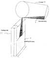
- a crucible ( 1 )is used in conjunction with a flat, rectangularly shaped casting mold ( 2 ).
- the mold ( 2 )has a major axis (j) and a minor axis (i) formed by 2 large flat surfaces spaced apart a distance (t) wherein j>i>t.
- This moldis open at the top as shown in the drawing.
- the resulting geometrically shaped object formed in the moldis referred to herein as a planar rectangular plate with parallel faces and conforms substantially to the final size, shape and dimensions of the silicon-aluminum target body.
- the meltis poured into the mold at the top through the opening of the dimension (t) as shown in the drawing.
- the silicon material used for purposes of the present inventioncan be any suitable silicon typically used for preparation of sputtering targets. These are typically identified as 2N5 to 5N purity granules or broken scraps from the semiconductor industry.
- the aluminum compoundis likewise preferred to be 2N5 to 5N purity.
- the melt of the silicon and aluminum in the crucibletakes place at about 1500° C. with a casting temperature of about 1450° C.
- the crucibleitself can be graphite or aluminum.
- a crucible size of about 20 litershas been found to be convenient.
- a vacuum induction furnace having a maximum power of 120 kW for 20 litersis sufficient.
- the atmosphere in the furnaceis kept around 1 ⁇ 10 ⁇ 1 mbar vacuum. Generally, if starting with a cold crucible, it takes about 2 hours to reach process time.
- the mold temperatureis generally at room temperature before casting.
- the casting timeis ⁇ fraction (1/2 ) ⁇ to 2 minutes per mold, preferably 1 to 2 minutes.
- the moldhas a rectangular shape with two larger flat surfaces of the dimension j ⁇ i separated a distance, t, by 2 narrow flat surfaces of the dimension i ⁇ j.
- This configuration of the mold with the relatively large flat surfaces separated a relatively small distance, t, from each other and with the top of the mold openenables the pouring of the molten melt into the mold and the solidification of the melt in a rapid cooling step into the superior target material of this invention.
- the purity of the aluminumis 2N5 to 5N purity.
- Target tiles with a size of 100 ⁇ 100 ⁇ 14 mm in each casewere prepared from tiles with a 1 wt %, 5 wt %, 10 wt % and 15 wt % aluminum content by grinding the surfaces and separation by means of a diamond separating disk. The density was determined in each case in order to characterize the casting defects.
- German priority application 198 10 246.1is relied on and incorporated herein by reference.
Landscapes
- Chemical & Material Sciences (AREA)
- Engineering & Computer Science (AREA)
- Mechanical Engineering (AREA)
- Chemical Kinetics & Catalysis (AREA)
- Materials Engineering (AREA)
- Metallurgy (AREA)
- Organic Chemistry (AREA)
- Physical Vapour Deposition (AREA)
Abstract
Description
- This is a continuation-in-part of our copending application No. 09/261,211 filed Mar. 3, 1999 which is relied on and incorporated herein by reference.[0001]
- The present invention relates to a sputtering target for depositing silicon layers in their nitride or oxide form by means of reactive cathode atomization, such as e.g. Si[0002]3N4or SiO2in the form of optical functional layers on glass substrates. More particularly, according to the present invention, the target material is a cast silicon element, that has been solidified from the melt condition, with an additive mixed in with the melt. In another aspect, the present invention relates to a process for preparation of the aforesaid sputtering target and products obtained thereby
- Thin silicon layers in their nitride and oxide form are becoming increasingly important in modem glass coating processes. In particular, the technology is important in the fields of optical coatings on large glass surfaces, as well as architectural, automotive and anti-reflective glass. These layers are usually applied by means of sputtering technology. A Si[0003]3N4-like or SiO2-like layer is deposited from a lightly doped silicon target via the extra addition of N2, as the reactive gas. For flat sputtering cathodes, use is usually made of highly pure, polycrystalline, boron-doped or phosphorus-doped silicon as the target material.
- A process is known for the application of optically transparent layers, which comprise compounds of silicon on planar substrates, by means of reactive cathode atomization of silicon-containing target materials (EP 0,165,413). In that process a cast polycrystalline silicon molded element, which solidified from the melted condition, and which comprises at least 99% silicon together with dopants selected from the boron, antimony, phosphorus and arsenic group that are mixed into the melt, is atomized in an atmosphere which contains a reactive gas selected from the group oxygen and nitrogen, by means of a direct current.[0004]
- With prior technology, the boron or phosphorus doped polycrystalline silicon tiles have been found to be rather brittle and expensive. For example, such targets can only be used as bonded targets. Moreover, such targets are in short supply because they are predominantly produced for photovoltaic wafers, instead of sputtering targets.[0005]
- It is also known that plasma-sprayed silicon targets can be used for rotating cathodes on tubular steel supports. U.S. Pat. No. 5,853,816 shows that aluminum can be added to silicon sputter targets but points out that with aluminum insufficient homogeneity cause arcing of the SiAl target. The reference proposes to produce silicon particles coated with a conductive material such as Al, Ni or an Al—Ni alloy and then vacuum plasma spraying these particles onto the sputtering target carrier.[0006]
- The highly pure, silicon target material, that is used for flat cathodes, is generally obtained as a by-product from the preparation of silicon slices for photovoltaic technology. For this purpose, slowly crystallized tiles are reworked for equipping the cathode. These tiles are then joined together by soldering or adhesion techniques to give a large cathode. The tiles produced in this way are more expensive in production, and they are brittle and therefore easily cracked by sputtering or in handling. A considerable problem occurs because these prior known titles need to be bonded; i.e., soldered, to a metallic backing plate for fixation in the sputter machine. The reason that such tiles are expensive is because they are produced by a very time consuming melting process and by an expensive cutting and grinding process.[0007]
- A sputtering target is also known, especially with large dimensions and comprising brittle materials such as e.g. Si, Ge, ln[0008]2O3and SnO2(DE-OS 19,527,476), which consists of a target base plate and a layer, which is arranged between the sputtering material and the base plate. The layer comprises an adhesive, preferably an epoxy resin adhesive, which has been mixed with a metal powder, whereby the target material is applied directly to the base plate with the intermediate inclusion of the adhesive layer, and the metal powder is formed from copper, nickel, gold or iron.
- Finally, a target is known for the cathode of a device for coating work pieces (DE-OS 4,242,079), where the cathode is arranged in a processing chamber, which is capable of being evacuated and filled with a processing gas, together with a cathode element and with a number of target tiles. These are contiguously arranged in a row on the cathode element and which collectively form the target. There is at least one target base plate, which is arranged between the target tiles and the cathode element, whereby the target tiles, that are formed from the material that is to be sputtered off, each have a plate like or parallelepiped configuration with plane parallel faces and are firmly soldered, welded or glued in each case to a target base plate with similar dimensions. The base surfaces of the target base plates are designed to be slightly larger in their length than the base surface of the target tiles that are associated therewith in each case, whereby the two edge parts across the breadth of the target base plate, which project beyond the edge of the target tiles in each case, are held firmly on the cathode element with the help of grasping clips.[0009]
- An object of the present invention is to create a target which is suitable for the preparation of silicon layers in their oxide or nitride form on a glass surface and which, in particular, is especially inexpensively capable of being molded into the configuration of tiles.[0010]
- It is a further object of the present invention to avoid the need for bonding silicon sputtering targets to a base plate.[0011]
- The above and other objects of the invention can be achieved by a target material which comprises silicon with the additive concentration of 1 wt % to 15 wt % aluminum. A molten melt of the silicon and aluminum is prepared. This material is then cast into a flat mold, which can take the shape of a tile on the solidified melt, preferably the configuration of a flat planar molded element with parallel faces.[0012]
- The basic target material, to which the concentration of the aluminum has been mixed in with the silicon, is cast in a flat casting mold which is close to the final size of the desired target. The solidified semi-finished products, which have been cast closely to their final size, can be reworked into individual target tiles at comparatively low expense in terms of a minimum of grinding or cutting and are then assembled to provide the desired configuration.[0013]
- Surprisingly, it has been found with sputtering targets comprising these cast silicon-aluminum tiles, which are close to the final size, that silicon oxide or silicon nitride layers can be sputtered with comparable optical parameters despite the casting defects, that are present, such as micro-pores and micro-fissures and despite the high aluminum doping level.[0014]
- The present invention will be further understood with reference to the accompanying drawing which is a schematic representation of carrying out the process of the invention.[0015]
- In carrying out the present invention there is added aluminum to silicon in the amount of 1 to 15%, preferably 7 to 10% by weight. The resulting mixture is cast into a flat planar casting mold and thereby a cost effective production process can be achieved. The addition of aluminum reduces the fragility of the target. By the present invention it is possible to eliminate the bonding of the target to a backing plate. In this way the targets produced according to the invention can be used as clamped, non-bonded target tiles.[0016]
- In accordance with the process feature of the present invention, the equipment used for purposes of carrying out the invention is schematically illustrated in the accompanying drawing wherein a crucible ([0017]1) is used in conjunction with a flat, rectangularly shaped casting mold (2). The mold (2) has a major axis (j) and a minor axis (i) formed by 2 large flat surfaces spaced apart a distance (t) wherein j>i>t. This mold is open at the top as shown in the drawing. The resulting geometrically shaped object formed in the mold is referred to herein as a planar rectangular plate with parallel faces and conforms substantially to the final size, shape and dimensions of the silicon-aluminum target body. The melt is poured into the mold at the top through the opening of the dimension (t) as shown in the drawing.
- The silicon material used for purposes of the present invention can be any suitable silicon typically used for preparation of sputtering targets. These are typically identified as 2N5 to 5N purity granules or broken scraps from the semiconductor industry. The aluminum compound is likewise preferred to be 2N5 to 5N purity.[0018]
- The melt of the silicon and aluminum in the crucible takes place at about 1500° C. with a casting temperature of about 1450° C. The crucible itself can be graphite or aluminum. A crucible size of about 20 liters has been found to be convenient.[0019]
- A vacuum induction furnace having a maximum power of 120 kW for 20 liters is sufficient. The atmosphere in the furnace is kept around 1×10[0020]−1mbar vacuum. Generally, if starting with a cold crucible, it takes about 2 hours to reach process time. The mold temperature is generally at room temperature before casting.
- With a 20 liter crucible size, it is possible to fill about 10 molds, if the furnace is equipped with a lock-in chamber. The casting time is {fraction (1/2 )}to 2 minutes per mold, preferably 1 to 2 minutes.[0021]
- As shown in the drawing, the mold has a rectangular shape with two larger flat surfaces of the dimension j×i separated a distance, t, by 2 narrow flat surfaces of the dimension i×j. This configuration of the mold with the relatively large flat surfaces separated a relatively small distance, t, from each other and with the top of the mold open enables the pouring of the molten melt into the mold and the solidification of the melt in a rapid cooling step into the superior target material of this invention.[0022]
- Casting of silicon in a wide open conventional mold with slow cooling time produces a product having cracks all over. While the presence of aluminum makes is possible to reduce the problem of cracking, it is really the mold configuration of a flat parallelepiped casting mold as shown in the drawing that overcomes the problems of the prior art.[0023]
- It is an important feature of the present invention that the tiles produced as described herein can be used as clamped targets without being bonded to a backing plate. This enables the following advantages to flow to the users as a result of the invention:[0024]
- a) quick and easy target exchanger at the time when a target is sputtered through;[0025]
- b) the user does not need the infrastructure for bonding targets to a base plate thereby eliminating the need to send the target out to a commercial bond shop and the resultant savings afforded thereby, and[0026]
- c) the user does not need to keep several sets of based plates in stock.[0027]
- Various alloys, which comprised industrially pure silicon and aluminum, i.e. 99.5% purity with respect to the metal in each case, were melted in a vacuum induction oven. Graphite was used as the crucible material. The receptacle used as the casting mold had the following dimensions: width 110 mm, thickness 16 mm and height 330 mm. The casting mold, of graphite was preheated to approximately 200° C. And was introduced into the vacuum oven through sluices directly before casting.[0028]
- The following alloys were melted:[0029]
- a) Si 99.5% purity without Al doping[0030]
- b) Si 99.5% purity +1 wt % Al[0031]
- c) Si 99.5% purity +5 wt % Al[0032]
- d) Si 99.5% purity +10 wt % Al[0033]
- e) Si 99.5% purity +15 wt % Al[0034]
- The purity of the aluminum is 2N5 to 5N purity.[0035]
- Whereas with pure silicon (Example a), only completely broken up cast components were capable of being prepared, even after varying the deposition conditions, it was possible to produce intact plates starting from alloying levels of only 1 wt % Al. However, the cast plates with 1 wt % Al proved to be extremely sensitive to fissures during processing by means of grinding and sawing.[0036]
- Target tiles with a size of 100×100×14 mm in each case were prepared from tiles with a 1 wt %, 5 wt %, 10 wt % and 15 wt % aluminum content by grinding the surfaces and separation by means of a diamond separating disk. The density was determined in each case in order to characterize the casting defects.[0037]
- Sputtering experiments with 5 wt % Al, 10 wt % Al and 15 wt % Al resulted in completely comparable optical parameters compared with thin silicon layers in their oxide or nitride form which had been prepared from highly pure silicon. The significant results are summarized in the table below:[0038]
Mea- Index of Theo- sured refraction at retical den- 550 nm Index at 550 Cracking density sity Si3N4 nm SiO2 risk Pure Silicon 2.33 n.a. 2.05 ± 0.05 1.46 ± 0.02 Extreme Si + 1 wt % 2.33 2.18 — — Very high Si + 5 wt % 2.35 2.26 2.05 ± 0.05 1.47 ± 0.02 High Si + 10 wt % 2.36 2.33 2.05 ± 0.05 1.48 ± 0.02 Low Si + 15 wt % 2.38 2.37 — 1.50 ± 0.02 Low - Further variations and modifications of the foregoing will be apparent to those skilled in the art and are intended to be encompassed by the claims appended hereto.[0039]
- German priority application 198 10 246.1 is relied on and incorporated herein by reference.[0040]
Claims (10)
Priority Applications (2)
| Application Number | Priority Date | Filing Date | Title |
|---|---|---|---|
| US09/829,434US6581669B2 (en) | 1998-03-10 | 2001-04-10 | Sputtering target for depositing silicon layers in their nitride or oxide form and a process for its preparation |
| US10/396,148US20030183508A1 (en) | 1999-03-03 | 2003-03-25 | Sputtering target for depositing silicon layers in their nitride or oxide form and process for its preparation |
Applications Claiming Priority (5)
| Application Number | Priority Date | Filing Date | Title |
|---|---|---|---|
| DE19810246.1 | 1998-03-10 | ||
| DE19810246ADE19810246A1 (en) | 1998-03-10 | 1998-03-10 | Sputtering target for the deposition of nitridic or oxidic silicon layers and process for its production |
| DE19810246 | 1998-03-10 | ||
| US26121199A | 1999-03-03 | 1999-03-03 | |
| US09/829,434US6581669B2 (en) | 1998-03-10 | 2001-04-10 | Sputtering target for depositing silicon layers in their nitride or oxide form and a process for its preparation |
Related Parent Applications (1)
| Application Number | Title | Priority Date | Filing Date |
|---|---|---|---|
| US26121199AContinuation-In-Part | 1998-03-10 | 1999-03-03 |
Related Child Applications (1)
| Application Number | Title | Priority Date | Filing Date |
|---|---|---|---|
| US10/396,148Continuation-In-PartUS20030183508A1 (en) | 1999-03-03 | 2003-03-25 | Sputtering target for depositing silicon layers in their nitride or oxide form and process for its preparation |
Publications (2)
| Publication Number | Publication Date |
|---|---|
| US20020008021A1true US20020008021A1 (en) | 2002-01-24 |
| US6581669B2 US6581669B2 (en) | 2003-06-24 |
Family
ID=26044501
Family Applications (1)
| Application Number | Title | Priority Date | Filing Date |
|---|---|---|---|
| US09/829,434Expired - Fee RelatedUS6581669B2 (en) | 1998-03-10 | 2001-04-10 | Sputtering target for depositing silicon layers in their nitride or oxide form and a process for its preparation |
Country Status (1)
| Country | Link |
|---|---|
| US (1) | US6581669B2 (en) |
Cited By (10)
| Publication number | Priority date | Publication date | Assignee | Title |
|---|---|---|---|---|
| US20020076452A1 (en)* | 2000-08-01 | 2002-06-20 | Ashni Naturaceuticals, Inc. | Combinations of sesquiterpene lactones and ditepene lactones or triterpenes for synergistic inhibition of cyclooxygenase-2 |
| US20020171123A1 (en)* | 2001-05-21 | 2002-11-21 | Apostolos Voutsas | System and method for fabricating silicon targets |
| US20040062675A1 (en)* | 2002-06-07 | 2004-04-01 | Wenjun Zhang | Fabrication of ductile intermetallic sputtering targets |
| US20040158309A1 (en)* | 2003-02-10 | 2004-08-12 | W. C. Heraeus Gmbh & Co. Kg | Metal alloy for medical devices and implants |
| EP1447458A3 (en)* | 2002-11-14 | 2004-08-25 | W.C. Heraeus GmbH & Co. KG | process for producing a Si-based alloy sputtering target, sputtering target and its application |
| US20070276488A1 (en)* | 2003-02-10 | 2007-11-29 | Jurgen Wachter | Medical implant or device |
| US20080038146A1 (en)* | 2003-02-10 | 2008-02-14 | Jurgen Wachter | Metal alloy for medical devices and implants |
| US20080138502A1 (en)* | 2006-12-11 | 2008-06-12 | Roland Trassl | Method for the production of an sin:h layer on a substrate |
| US20100252418A1 (en)* | 2009-04-07 | 2010-10-07 | Magna Mirrors Of America, Inc. | Hot tile sputtering system |
| CN111531172A (en)* | 2020-05-29 | 2020-08-14 | 同济大学 | 3D printing process method of high-strength aluminum-silicon alloy |
Families Citing this family (6)
| Publication number | Priority date | Publication date | Assignee | Title |
|---|---|---|---|---|
| US20060207740A1 (en)* | 2002-11-14 | 2006-09-21 | Martin Weigert | Processes for producing a sputtering target from a silicon-based alloy, a sputtering target |
| US20050196632A1 (en)* | 2003-12-18 | 2005-09-08 | Afg Industries, Inc. | Protective layer for optical coatings with enhanced corrosion and scratch resistance |
| BRPI0609103A2 (en) | 2005-05-12 | 2010-02-17 | Agc Flat Glass Na Inc | low emissivity coating with low solar heating coefficient and optimized chemical and mechanical properties, and production process thereof |
| US20070007505A1 (en)* | 2005-07-07 | 2007-01-11 | Honeywell International Inc. | Chalcogenide PVD components |
| US20090065354A1 (en)* | 2007-09-12 | 2009-03-12 | Kardokus Janine K | Sputtering targets comprising a novel manufacturing design, methods of production and uses thereof |
| US7901781B2 (en) | 2007-11-23 | 2011-03-08 | Agc Flat Glass North America, Inc. | Low emissivity coating with low solar heat gain coefficient, enhanced chemical and mechanical properties and method of making the same |
Family Cites Families (11)
| Publication number | Priority date | Publication date | Assignee | Title |
|---|---|---|---|---|
| JPS52144313A (en)* | 1976-05-28 | 1977-12-01 | Hitachi Ltd | Transmission material with relative sliding having excellent pitting resistance and its production |
| DE3417732A1 (en) | 1984-05-12 | 1986-07-10 | Leybold-Heraeus GmbH, 5000 Köln | METHOD FOR APPLYING SILICON-CONTAINING LAYERS TO SUBSTRATES BY CATODIZING AND SPRAYING CATODE FOR CARRYING OUT THE METHOD |
| US4769291A (en)* | 1987-02-02 | 1988-09-06 | The Boc Group, Inc. | Transparent coatings by reactive sputtering |
| JPH04184732A (en)* | 1990-11-20 | 1992-07-01 | Seiko Epson Corp | Sputtering target and protective film using the sputtering target |
| US5094288A (en)* | 1990-11-21 | 1992-03-10 | Silicon Casting, Inc. | Method of making an essentially void-free, cast silicon and aluminum product |
| BE1007067A3 (en) | 1992-07-15 | 1995-03-07 | Emiel Vanderstraeten Besloten | SPUTTER CATHOD AND METHOD FOR MANUFACTURING THIS CATHOD |
| US5328585A (en)* | 1992-12-11 | 1994-07-12 | Photran Corporation | Linear planar-magnetron sputtering apparatus with reciprocating magnet-array |
| DE4242079A1 (en) | 1992-12-14 | 1994-06-16 | Leybold Ag | Target for a cathode arranged in an evacuable process chamber floodable with a process gas |
| JPH08193236A (en)* | 1995-01-18 | 1996-07-30 | Sumitomo Electric Ind Ltd | High toughness wear-resistant aluminum alloy and method for producing the same |
| DE19527476A1 (en) | 1995-07-27 | 1997-01-30 | Leybold Ag | Sputtering target with highly adherent sputtering material - bonded to base plate by inexpensive metal powder-contg. epoxide adhesive |
| US6045634A (en)* | 1997-08-14 | 2000-04-04 | Praxair S. T. Technology, Inc. | High purity titanium sputtering target and method of making |
- 2001
- 2001-04-10USUS09/829,434patent/US6581669B2/ennot_activeExpired - Fee Related
Cited By (18)
| Publication number | Priority date | Publication date | Assignee | Title |
|---|---|---|---|---|
| US20020076452A1 (en)* | 2000-08-01 | 2002-06-20 | Ashni Naturaceuticals, Inc. | Combinations of sesquiterpene lactones and ditepene lactones or triterpenes for synergistic inhibition of cyclooxygenase-2 |
| US20020171123A1 (en)* | 2001-05-21 | 2002-11-21 | Apostolos Voutsas | System and method for fabricating silicon targets |
| US6673220B2 (en)* | 2001-05-21 | 2004-01-06 | Sharp Laboratories Of America, Inc. | System and method for fabricating silicon targets |
| US20040062675A1 (en)* | 2002-06-07 | 2004-04-01 | Wenjun Zhang | Fabrication of ductile intermetallic sputtering targets |
| EP1447458A3 (en)* | 2002-11-14 | 2004-08-25 | W.C. Heraeus GmbH & Co. KG | process for producing a Si-based alloy sputtering target, sputtering target and its application |
| US20080038146A1 (en)* | 2003-02-10 | 2008-02-14 | Jurgen Wachter | Metal alloy for medical devices and implants |
| US20070221300A1 (en)* | 2003-02-10 | 2007-09-27 | Jurgen Wachter | Metal alloy for medical devices and implants |
| US20070276488A1 (en)* | 2003-02-10 | 2007-11-29 | Jurgen Wachter | Medical implant or device |
| US20040158309A1 (en)* | 2003-02-10 | 2004-08-12 | W. C. Heraeus Gmbh & Co. Kg | Metal alloy for medical devices and implants |
| US20100222866A1 (en)* | 2003-02-10 | 2010-09-02 | Jurgen Wachter | Metal alloy for medical devices and implants |
| US8349249B2 (en) | 2003-02-10 | 2013-01-08 | Heraeus Precious Metals Gmbh & Co. Kg | Metal alloy for medical devices and implants |
| US8403980B2 (en) | 2003-02-10 | 2013-03-26 | Heraeus Materials Technology Gmbh & Co. Kg | Metal alloy for medical devices and implants |
| US20080138502A1 (en)* | 2006-12-11 | 2008-06-12 | Roland Trassl | Method for the production of an sin:h layer on a substrate |
| EP1933391A1 (en)* | 2006-12-11 | 2008-06-18 | Applied Materials, Inc. | Method for forming an SiN:H layer on a substrate |
| US20100252418A1 (en)* | 2009-04-07 | 2010-10-07 | Magna Mirrors Of America, Inc. | Hot tile sputtering system |
| US8673122B2 (en)* | 2009-04-07 | 2014-03-18 | Magna Mirrors Of America, Inc. | Hot tile sputtering system |
| US9476117B2 (en) | 2009-04-07 | 2016-10-25 | Magna Mirrors Of America, Inc. | Hot tile sputtering system |
| CN111531172A (en)* | 2020-05-29 | 2020-08-14 | 同济大学 | 3D printing process method of high-strength aluminum-silicon alloy |
Also Published As
| Publication number | Publication date |
|---|---|
| US6581669B2 (en) | 2003-06-24 |
Similar Documents
| Publication | Publication Date | Title |
|---|---|---|
| US6581669B2 (en) | Sputtering target for depositing silicon layers in their nitride or oxide form and a process for its preparation | |
| US4978437A (en) | Method of applying optical coatings of silicon compounds by cathode sputtering, and a sputtering cathode for the practice of the method | |
| RU2303663C2 (en) | Receiving vessel for melt silicon or vessel for melting silicon and method for making it | |
| US8173093B2 (en) | Iron silicide sputtering target and method for production thereof | |
| EP0869102B1 (en) | Process and apparatus for preparing polycrystalline silicon and process for preparing silicon substrate for solar cell | |
| US20120045360A1 (en) | Cu-ga alloy sputtering target and manufacturing method thereof | |
| US5965278A (en) | Method of making cathode targets comprising silicon | |
| KR102492076B1 (en) | Coating material for high-purity aluminum smelting casting and its manufacturing method and use | |
| EP2025780A2 (en) | Silicon release coating, method of making same, and method of using same | |
| US20030183508A1 (en) | Sputtering target for depositing silicon layers in their nitride or oxide form and process for its preparation | |
| JP2014084515A (en) | FABRICATION METHOD FOR Cu-Ga ALLOY SPUTTERING TARGET, AND Cu-Ga ALLOY SPUTTERING TARGET | |
| US5143541A (en) | Process for producing powdered metal spray coating material | |
| JP3981538B2 (en) | Silicon holding container and manufacturing method thereof | |
| US20170169998A1 (en) | In-Cu Alloy Sputtering Target And Method For Producing The Same | |
| JP2000026961A (en) | Sputtering target and its production | |
| WO2004057052A1 (en) | Resistance-heated boat and manufacturing method thereof | |
| CN101748307A (en) | Gold-arsenic alloy material and preparation method thereof | |
| US6478895B1 (en) | Nickel-titanium sputter target alloy | |
| US3877913A (en) | Method of making a cathode for RF sputtering amorphous semiconducting thin films | |
| JPS58164780A (en) | Formation of target for sputtering | |
| JPH04184732A (en) | Sputtering target and protective film using the sputtering target | |
| JP3468137B2 (en) | Sputtering target for optical recording medium protective film formation without spatter cracking | |
| KR100274737B1 (en) | Manufacturing method of sputtering target | |
| CN119216865A (en) | A sputtering target assembly with a back plate in a vacuum environment and a bonding composite solder and a welding process thereof | |
| JPS6320153A (en) | Production of alloy target |
Legal Events
| Date | Code | Title | Description |
|---|---|---|---|
| AS | Assignment | Owner name:UNAXIS MATERIALS DEUTSCHLAND GMBH, GERMANY Free format text:ASSIGNMENT OF ASSIGNORS INTEREST;ASSIGNORS:WEIGERT, MARTIN;KONIETZKA, UWE;REEL/FRAME:012008/0259 Effective date:20010319 | |
| AS | Assignment | Owner name:HERAEUS THINFILM MATERIALS GMBH, GERMANY Free format text:CHANGE OF NAME;ASSIGNOR:UNAXIS MATERIALS DEUTSCHLAND GMBH;REEL/FRAME:013590/0875 Effective date:20020719 | |
| AS | Assignment | Owner name:W.C. HERAEUS GMBH & CO. KG, GERMANY Free format text:ASSIGNMENT OF ASSIGNORS INTEREST;ASSIGNOR:HERAEUS THINFILM MATERIALS GMBH;REEL/FRAME:013835/0035 Effective date:20030205 | |
| FEPP | Fee payment procedure | Free format text:PAYOR NUMBER ASSIGNED (ORIGINAL EVENT CODE: ASPN); ENTITY STATUS OF PATENT OWNER: LARGE ENTITY | |
| FPAY | Fee payment | Year of fee payment:4 | |
| FPAY | Fee payment | Year of fee payment:8 | |
| AS | Assignment | Owner name:W.C. HERAEUS GMBH, GERMANY Free format text:CHANGE OF NAME;ASSIGNOR:W.C. HERAEUS GMBH & CO.KG;REEL/FRAME:027819/0282 Effective date:20040826 | |
| AS | Assignment | Owner name:HERAEUS MATERIALS TECHNOLOGY GMBH & CO. KG, GERMAN Free format text:CHANGE OF NAME;ASSIGNOR:W.C. HERAEUS GMBH;REEL/FRAME:027830/0077 Effective date:20110718 | |
| REMI | Maintenance fee reminder mailed | ||
| LAPS | Lapse for failure to pay maintenance fees | ||
| LAPS | Lapse for failure to pay maintenance fees | Free format text:PATENT EXPIRED FOR FAILURE TO PAY MAINTENANCE FEES (ORIGINAL EVENT CODE: EXP.) | |
| FP | Lapsed due to failure to pay maintenance fee | Effective date:20150624 | |
| STCH | Information on status: patent discontinuation | Free format text:PATENT EXPIRED DUE TO NONPAYMENT OF MAINTENANCE FEES UNDER 37 CFR 1.362 |